

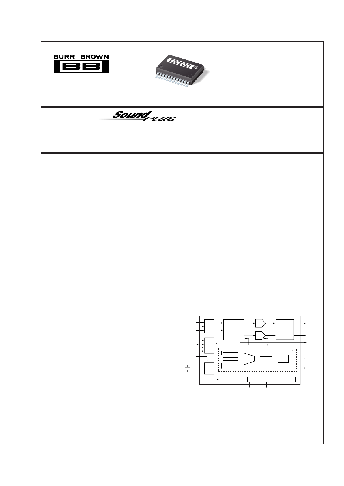
Burr Brown PCM1740E, PCM1740E-2K Datasheet
®
1
PCM1740
Stereo Audio
DIGITAL-TO-ANALOG CONVERTER
with VCXO and PLL
PCM1740
®
FEATURES
● COMPLETE DELTA-SIGMA STEREO DAC
● VOLTAGE-CONTROLLED CRYSTAL
OSCILLATOR: 27MHz ±150ppm Output with
0V to 3V Input
● PROGRAMMABLE PLL
256fS or 384fS Audio System Clock Output
● DYNAMIC PERFORMANCE:
Dynamic Range: 94dB
SNR: 94dB
THD+N: –89dB
● SAMPLING FREQUENCIES:
16kHz, 22.05kHz, 24kHz
32kHz, 44.1kHz, 48kHz
64kHz, 88.2kHz, 96kHz
● SERIAL AUDIO INTERFACE:
Standard or I2S Data Formats
16-, 20-, or 24-Bit Data
● I2C-BUS® INTERFACE FOR CONTROL
REGISTERS
(1)
:
Slave Receiver Operation
7-Bit Addressing
Standard Transfer Rate (up to 100kbps)
● PROGRAMMABLE CONTROLS:
Digital Attenuation (256 steps)
Soft Mute
Infinite Zero Detect Mute
De-Emphasis (32kHz, 44.1kHz, 48kHz)
DAC Output Mode
● SINGLE +5V SUPPLY
● SMALL SSOP-24 PACKAGE
© 2000 Burr-Brown Corporation PDS-1551A Printed in U.S.A. February, 2000
For most current data sheet and other product
information, visit www.burr-brown.com
TM
DESCRIPTION
The PCM1740 is a complete stereo audio digital-to-analog
converter with on-chip PLL and VCXO. The PCM1740 is
designed specifically for set-top box applications requiring
high-quality audio playback, a precision tuned 27MHz master clock source, and support for multiple audio-sampling
frequencies.
The stereo D/A converter utilizes multi-bit, delta-sigma
architecture, which includes an 8x interpolation filter, thirdorder noise shaping, 5-level amplitude quantization, and an
analog low-pass filter. The PCM1740 includes a number of
user-programmable functions, which are accessed via a
standard I2C-Bus interface.
APPLICATIONS
● SET-TOP BOXES
● DIGITAL BROADCAST RECEIVERS
International Airport Industrial Park • Mailing Address: PO Box 11400, Tucson, AZ 85734 • Street Address: 6730 S. Tucson Blvd., Tucson, AZ 85706 • Tel: (520) 746-1111
Twx: 910-952-1111 • Internet: http://www.burr-brown.com/ • Cable: BBRCORP • Telex: 066-6491 • FAX: (520) 889-1510 • Immediate Product Info: (800) 548-6132
NOTE: (1) I2C-Bus® is a registered trademark of Philips Semiconductor.
PCM1740
PCM
Audio
I/F
I
2
C
I/F
and
REGs
VCXO
SCL
SDA
AD1
AD0
XTUN
XT1
XT2
RST
27MHz
Crystal
8x
Oversampling
Digital Filter
and
Sub-Functions
Process
DAC
(R)
Counter N
V
OUT
L
V
COM
ZERO
SCKO
(256f
S
/384fS)
MCKO
(27MHz)
V
OUT
R
Counter M
Power Supply
Reset
BCK
LRCK
DATA
Phase
Detector
V
PP
AGND DGNDV
CC
V
DD
PGND
DAC
(L)
Low-Pass
Filter
and Amp
LPF
VCO
®
2
PCM1740
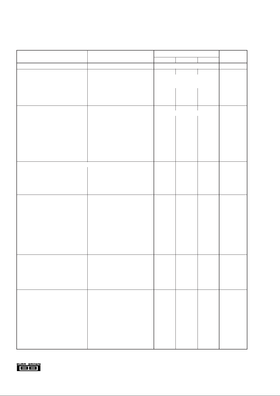
SPECIFICATIONS
All specifications at TA = +25°C, V
CC
= V
DD
= V
PP
= 5.0V, fS = 44.1kHz, system clock = 384fS, 16-bit data, unless otherwise noted.
PCM1740E
PARAMETER CONDITIONS MIN TYP MAX UNITS
RESOLUTION 16 Bits
DATA FORMAT
Audio Interface Format Standard/ I
2
S Selectable
Audio Data Bit Length 16/20/24 Selectable Bits
Audio Data Format MSB First, Two’s Binary Complement
Sampling Frequency (f
S
) Standard (fS) 32 44.1 48 kHz
Half (fS) 16 22.05 24 kHz
Double (f
S
) 64 88.2 96 kHz
Internal System Clock Frequency 256f
S
/384f
S
DIGITAL INPUT/OUTPUT
Logic Family Input Logic TTL Compatible
High Level Input Voltage: V
IH
(1), (2)
2.0 VDC
Low Level Input Voltage: V
IL
(1), (2)
0.8 VDC
High Level Input Current: I
IH
(1), (2)
VIH = V
DD
±10 µA
Low Level Input Current:
I
IL
(1)
VIL = 0V ±10 µA
I
IL
(2)
VIL = 0V –120 µA
High Level Output Voltage: V
OH
(3)
IOH = –2mA VDD – 0.5V VDC
Low Level Output Voltage:
V
OH
(3)
IOL = 4mA 0.5 VDC
V
OL
(4)
IOL = 2mA 0.5 VDC
DIGITAL INPUT/OUTPUT of I
2
C-BUS INTERFACE
High Level Input Voltage: V
IH
(5)
3.0 V
Low Level Input Voltage: V
IL
(5)
–0.3 1.5 V
Low Level Output Voltage: V
OL
(6)
0 0.4 V
Output Fall Time: t
OF
(7)
250 ns
Input Logic Current: I
I
(8)
10% to 90% of V
DD
–10 10 µA
Capacitance for each I/O pin: C
I
(5)
10 pF
VCXO CHARACTERISTICS (MCKO) 27MHz, Fundamental Crystal
Crystal Clock Frequency
(9)
27.0000 MHz
Crystal Clock Accuracy
(9)
±30 ppm
XTUN Tuning Voltage Range
(10)
0 3.0 V
XTUN Input Impedance
(10)
60 kΩ
Output Clock Frequency XTUN = 1.3V 27.0000 MHz
Output Clock Accuracy XTUN = 1.3V ±50 ppm
VCXO Tuning Range XTUN = 0V – 3V 300 ppm
Output Clock Duty Cycle 10pF Load 35 45 55 %
Output Clock Jitter Standard Deviation 100 ps
Output Rise Time 20% to 80% V
DD
, 10pF Load 4 ns
Output Fall Time 80% to 20% V
DD
, 10pF Load 4 ns
Response Time
(11)
10 µs
Power Up Time
(12)
5ms
PLL AC CHARACTERISTICS (SCKO)
Output Clock Frequency MCKO = 27.0MHz 4.096 36.864 MHz
Output Clock Duty Cycle 10pF Load 40 50 60 %
Output Clock Jitter Standard Deviation 150 ps
Output Rise Time 20% to 80% V
DD
, 10pF Load 4 ns
Output Fall Time 80% to 20% V
DD
, 10pF Load 4 ns
Frequency Transition Time
(13)
20 ms
Power Up Time
(14)
15 30 ms
DYNAMIC PERFORMANCE
(15)
THD+N:
V
OUT
= 0dB fS = 44.1kHz 0.0035 0.01 %
fS = 96kHz 0.007 %
V
OUT
= –60dB fS = 44.1kHz 0.0035 0.01 %
f
S
= 96kHz 0.007 %
Dynamic Range f
S
= 44.1kHz, EIAJ, A-Weighted 90 94 dB
f
S
= 96kHz, A-Weighted 90 dB
Signal-to-Noise Ratio
(16)
fS = 44.1kHz, EIAJ, A-weighted 90 94 dB
f
S
= 96kHz, A-weighted 90 dB
Channel Separation f
S
= 44.1kHz 88 92 dB
f
S
= 96kHz 88 dB
Level Linearity Error V
OUT
= –90dB ±1.0 dB
®
3
PCM1740
The information provided herein is believed to be reliable; however, BURR-BROWN assumes no responsibility for inaccuracies or omissions. BURR-BROWN assumes
no responsibility for the use of this information, and all use of such information shall be entirely at the user’s own risk. Prices and specifications are subject to change
without notice. No patent rights or licenses to any of the circuits described herein are implied or granted to any third party. BURR-BROWN does not authorize or warrant
any BURR-BROWN product for use in life support devices and/or systems.
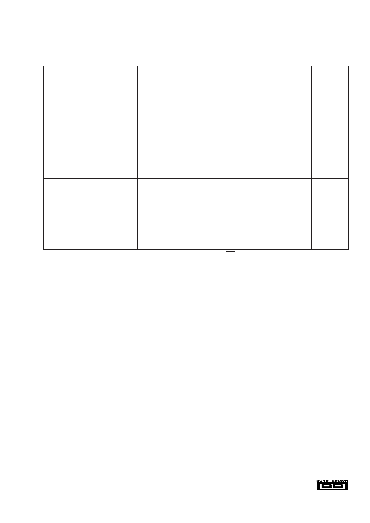
DC ACCURACY
Gain Error ±1.0 ±3.0 % of FSR
Gain Mismatch, Channel-to-Channel ±1.0 ±3.0 % of FSR
Bipolar Zero Error ±1.0 % of FSR
ANALOG OUTPUT
Voltage Range Full Scale (0dB) 0.62 V
CC
Vp-p
Center Voltage 0.5 V
CC
VDC
Load Impedance AC Coupled 5 kΩ
DIGITAL FILTER PERFORMANCE
Passband 0.445 f
S
Hz
Stopband 0.555 f
S
Hz
Passband Ripple ±0.17 dB
Stopband Attenuation –35 dB
De-Emphasis Error –0.2 +0.55 dB
Delay Time 11.125 / f
S
sec
ANALOG FILTER PERFORMANCE
Frequency Response 20Hz to 20kHz –0.16 dB
20Hz to 40kHz –0.6 dB
POWER SUPPLY REQUIREMENTS
Voltage Range V
DD
, VCC, V
PP
+4.5 +5 +5.5 VDC
Supply Current, I
DD
+ ICC + I
PP
VDD = VCC = V
PP
= +5V 25 30 mA
Power Dissipation V
DD
= VCC = V
PP
= +5V 125 150 mW
TEMPERATURE RANGE
Operation –25 +85 °C
Storage –55 +125 °C
Thermal Resistance,
θ
JA
100 °C/W
NOTES: (1) Pins 6, 7, 18, 19: AD0, AD1, BCK, DATA, LRCK (Schmitt trigger input). (2) Pin 10: RST (Schmitt trigger input with internal pull-up resistor). (3) Pins
5, 21: MCKO, SCKO. (4) Pin 16: ZERO (open drain output). (5) Pins 8, 9: SCL, SDA. (6) Pin 9: SDA (open drain output, I
OL
= 3mA). (7) Pin 9: SDA (from V
IHMIN
to V
ILMAX
with a bus capacitance from 10pF to 400pF). (8) Pins 8, 9: SCL, SDA (input current each I/O pin with an input voltage between 0.1VDD and 0.9VDD).
(9) This characteristic is the requirement for crystal oscillator. (10) Pin 3: XTUN. (11) The maximum response time when the XTUN is changed. (12) The maximum
delay time from power on to oscillation. (13) The maximum lock up time when the PLL frequency is changed. (14) The maximum delay time from power on to lock
up. (15) Dynamic performance specifications are tested with a 20kHz low-pass filter using a Shibasoku distortion analyzer 725°C with 30kHz LPF, 400Hz HPF,
Average-Mode. (16) SNR is tested with infinite zero detection circuit disabled.
PCM1740E
PARAMETER CONDITIONS MIN TYP MAX UNITS
SPECIFICATIONS
All specifications at TA = +25°C, V
CC
= V
DD
= V
PP
= 5.0V, fS = 44.1kHz, system clock = 384fS, 16-bit data, unless otherwise noted.
®
4
PCM1740
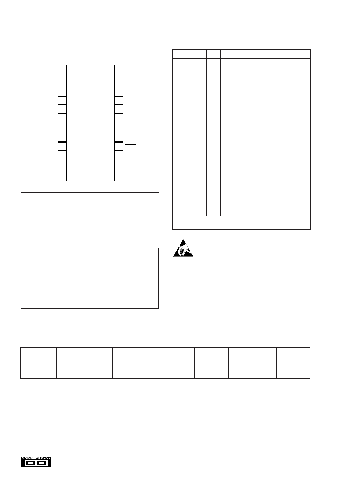
PIN NAME I/O FUNCTION
1 XT1 — 27MHz Crystal connection.
2 PGND — PLL and VCXO ground.
3 XTUN IN VCXO tune, tuning voltage range from 0V to 3V.
4V
PP
— PLL and VCXO power supply, +5V.
5 MCKO OUT Buffered clock output of VCXO.
6 AD0 IN Device address pin for I
2
C-BUS.
(1)
7 AD1 IN Device address pin for I2C-BUS.
(1)
8 SCL IN Bit clock input for I2C-BUS interface.
9 SDA
IN/OUT
Serial data for I2C-BUS interface.
10 RST IN Reset, active LOW.
(2)
11 V
OUT
R OUT Right-channel analog voltage output.
12 AGND — Analog ground.
13 V
CC
— Analog power supply, +5V.
14 V
OUT
L OUT Left-channel analog voltage output.
15 V
COM
— DC common-mode voltage output.
16 ZERO OUT Zero flag output, active LOW.
(3)
17 BCK IN Bit clock input for serial audio data.
(1)
18 DATA IN Serial audio data input.
(1)
19 LRCK IN Left and right word clock, equal to the sampling
rate (f
S
).
(1)
20 RSV — Reserved must be open.
21 SCKO OUT System clock output, 256/384 f
S
.
22 V
DD
— Digital power supply, +5V.
23 DGND — Digital ground.
24 XT2 — 27MHz Crystal connection.
NOTES: (1) Schmitt trigger input. (2) Schmitt trigger input with internal
pull-up resistor. (3) Open drain output.
Power Supply Voltage
(1)
...................................................................+6.5V
Supply Voltage Differences
(2)
........................................................... ±0.1V
GND Voltage Differences
(3)
.............................................................. ±0.1V
Digital Input Voltage................................................. –0.3V to (V
DD
+ 0.3V)
Analog Input Voltage................................................–0.3V to (V
CC
+ 0.3V)
Input Current (any pins except supplies) ........................................ ±10mA
Operating Temperature Range ......................................... –25°C to +85°C
Storage Temperature...................................................... –55°C to +125°C
Junction Temperature .................................................................... +150°C
Lead Temperature (soldering, 5s).................................................. +260°C
Package Temperature (IR reflow, peak, 10s) ................................ +235°C
NOTES: (1) V
CC
, VDD, VPP. (2) Among VCC, VDD, VPP. (3) Among AGND, DGND,
and PGND. Stresses above those listed under Absolute Maximum Ratings may
cause permanent damage to the device. Exposure to absolute maximum
conditions for extended periods may affect device reliability.
PIN ASSIGNMENTSPIN CONFIGURATION
Top View SSOP
ABSOLUTE MAXIMUM RATINGS
ELECTROSTATIC
DISCHARGE SENSITIVITY
This integrated circuit can be damaged by ESD. Burr-Brown
recommends that all integrated circuits be handled with
appropriate precautions. Failure to observe proper handling
and installation procedures can cause damage.
ESD damage can range from subtle performance degradation
to complete device failure. Precision integrated circuits may
be more susceptible to damage because very small parametric
changes could cause the device not to meet its published
specifications.
PACKAGE SPECIFIED
DRAWING TEMPERATURE PACKAGE ORDERING TRANSPORT
PRODUCT PACKAGE NUMBER RANGE MARKING NUMBER
(1)
MEDIA
PCM1740E SSOP-24 338 –25°C to +85°C PCM1740E PCM1740E Rails
" " " " PCM1740E PCM1740E/2K Tape and Reel
NOTE: (1) Models with a slash (/) are available only in Tape and Reel in the quantities indicated (e.g., /2K indicates 2000 devices per reel). Ordering 2000 pieces
of “PCM1740E/2K” will get a single 2000-piece Tape and Reel.
PACKAGE/ORDERING INFORMATION
XT1
PGND
XTUN
V
PP
MCKO
AD0
AD1
SCL
SDA
RST
V
OUT
R
AGND
PCM1740
XT2
DGND
V
DD
SCKO
RSV
LRCK
DATA
BCK
ZERO
V
COM
V
OUT
L
V
CC
1
2
3
4
5
6
7
8
9
10
11
12
24
23
22
21
20
19
18
17
16
15
14
13

®
5
PCM1740
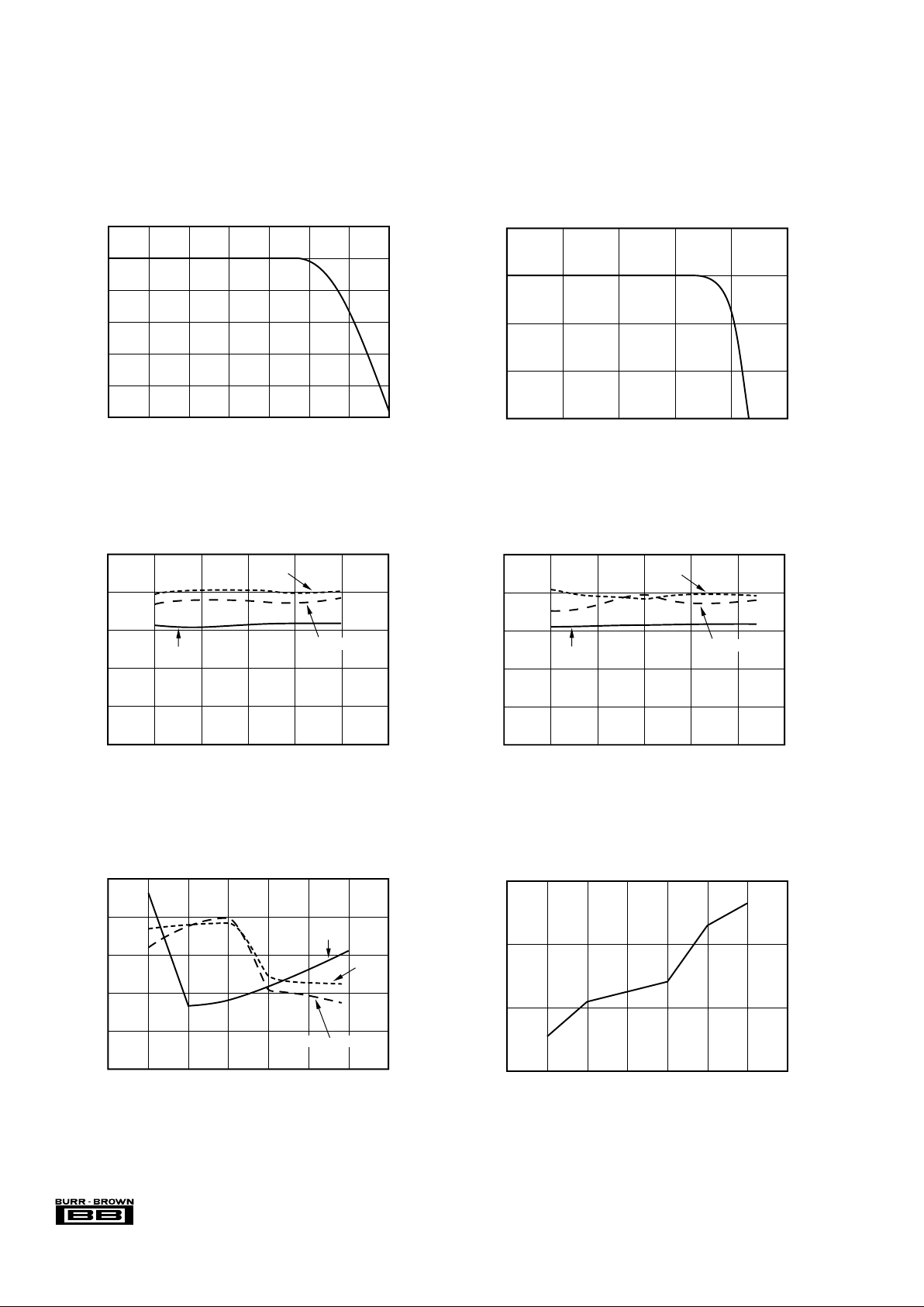
TYPICAL PERFORMANCE CURVES
At TA = +25°C, VCC = VDD = +5V, fS = 44.1kHz, F
SCKO
= 384fS = 16.9344MHz, and 16-bit data, unless otherwise noted.
FREQUENCY RESPONSE
(De-emphasis OFF, f
S
= 44.1kHz)
f
S
Level (dB)
0
–20
–40
–60
–80
–100
01234
PASSBAND RIPPLE
(De-emphasis OFF, f
S
= 44.1kHz)
f
S
Level (dB)
0
–0.2
–0.4
–0.6
–0.8
–1
0 0.20.1 0.3 0.4 0.5
DE-EMPHASIS FREQUENCY RESPONSE (3kHz)
0 5k 10k 15k 20k 25k
Frequency (Hz)
0
–2
–4
–6
–8
–10
–12
DE-EMPHASIS FREQUENCY RESPONSE (44.1kHz)
0 5k 10k 15k 20k 25k
Frequency (Hz)
0
–2
–4
–6
–8
–10
–12
DE-EMPHASIS FREQUENCY RESPONSE (48kHz)
0 5k 10k 15k 20k 25k
Frequency (Hz)
0
–2
–4
–6
–8
–10
–12
Level (dB) Level (dB) Level (dB)
DE-EMPHASIS ERROR (3kHz)
0 3628 7256 10884 14512
0 4999.8375 9999.675 14999.5125 19999.35
0 5442 10884 16326 21768
Frequency (Hz)
0.6
0.4
0.2
0
–0.2
–0.4
–0.6
0.6
0.4
0.2
0
–0.2
–0.4
–0.6
0.6
0.4
0.2
0
–0.2
–0.4
–0.6
DE-EMPHASIS ERROR (44.1kHz)
Frequency (Hz)
DE-EMPHASIS ERROR (48kHz)
Frequency (Hz)
Error (dB) Error (dB) Error (dB)
®
6
PCM1740
TYPICAL PERFORMANCE CURVES (Cont.)
At TA = +25°C, VCC = VDD = +5V, fS = 44.1kHz, F
SCKO
= 384fS = 16.9344MHz, and 16-bit data, unless otherwise noted.
ANALOG FILTER
(1Hz to 10MHz)
Log Frequency (Hz)
Level (dB)
20
0
–20
–40
–60
–80
–100
0 0.20.1 0.1 0.3 0.40.4 0.5
ANALOG FILTER
(1Hz to 20kHz)
Log Frequency (Hz)
Level (dB)
0.05
0
–0.05
–0.1
–0.15
110 1k100 10k 100k
SUPPLY CURRENT vs SAMPLING FREQUENCY
Sampling Frequency (kHz)
Supply Current (mA)
35
30
25
20
32 64 88.244.1 48 96.0
THD+N (FS), DYNAMIC RANGE, and SNR
vs SUPPLY VOLTAGE
(Temperature = 25°C, 384f
S
, fS = 44.1kHz)
Supply Voltage (V)
THD+D (FS) (%)
0.005
0.004
0.003
0.002
0.001
0.000
Dynamic Range, SNR (dB)
95
94
93
92
91
90
4.25 4.5 5.254.75 5 5.5 5.75
SNR
THD+N
Dynamic Range
THD+N (FS), DYNAMIC RANGE, and SNR
vs TEMPERATURE
(V
CC
= VDD = VPP = 5V, 384fS, fS = 44.1kHz)
Temperature (°C)
THD+D (FS) (%)
0.005
0.004
0.003
0.002
0.001
0.000
Dynamic Range, SNR (dB)
95
94
93
92
91
90
–50 –25 500 25 75 100
SNR
THD+N
Dynamic Range
THD+N (FS), DYNAMIC RANGE, and SNR
vs SAMPLING FREQUENCY
Sampling Frequency (kHz)
THD+D (FS) (%)
0.010
0.008
0.006
0.004
0.002
0.000
Dynamic Range, SNR (dB)
96
94
92
90
88
86
32 64 88.244.1 48 96.0
SNR
THD+N
Dynamic Range
 Loading...