

24-Bit, 192kHz Sampling
Enhanced Multi-Level, Delta-Sigma, Audio
DIGITAL-TO-ANALOG CONVERTER
PCM1737
®
TM
DESCRIPTION
The PCM1737 is a CMOS, monolithic, integrated
circuit which includes stereo digital-to-analog converters and support circuitry in a small SSOP-28
package. The data converters utilize Burr-Brown’s
enhanced multi-level delta-sigma architecture, which
employs 4th-order noise shaping and 8-level amplitude quantization to achieve excellent dynamic performance and improved tolerance to clock jitter.
The PCM1737 accepts industry standard audio data
formats with 16- to 24-bit data, providing easy
interfacing to audio DSP and decoder chips. Sampling rates up to 192kHz are supported. A full set
of user-programmable functions are accessible through
a 4-wire serial control port which supports register
write and read back functions.
FEATURES
● 24-BIT RESOLUTION
●
ANALOG PERFORMANCE (VCC = +5V):
Dynamic Range: 106dB typ
SNR: 106dB typ
THD+N: 0.0015% typ
Full-Scale Output: 3.1Vp-p typ
●
4x/8x OVERSAMPLING DIGITAL FILTER:
Passband: 0.454f
S
Stopband: 0.546f
S
Stopband Attenuation: –82dB
Passband Ripple: ±0.002dB
● SAMPLING FREQUENCY: 10kHz to 192kHz
● SYSTEM CLOCK: 128, 192, 256, 384, 512, or
768fS with Auto Detect
● ACCEPTS 16-, 18-, 20-, AND 24-BIT AUDIO DATA
● DATA FORMATS: Standard, I2S, and Left-Justified
●
USER-PROGRAMMABLE MODE CONTROLS:
Digital Attenuation: 0dB to –63dB, 0.5dB/Step
Digital De-Emphasis
Digital Filter Roll-Off: Sharp or Slow
Soft Mute
Variable Oversampling for ∆Σ DACs
Zero Detect Mute
Zero Flags for Each Output
●
DUAL SUPPLY OPERATION:
+5V Analog, +3.3V Digital
●
5V TOLERANT DIGITAL INPUTS
●
SMALL SSOP-28 PACKAGE
© 1999 Burr-Brown Corporation PDS-1552C Printed in U.S.A. March, 2000
APPLICATIONS
● A/V RECEIVERS
● DVD MOVIE AND AUDIO PLAYERS
● DVD ADD-ON CARDS FOR HIGH-END PCs
● HDTV RECEIVERS
● CAR AUDIO SYSTEMS
● OTHER APPLICATIONS REQUIRING 24-BIT
AUDIO
International Airport Industrial Park • Mailing Address: PO Box 11400, Tucson, AZ 85734 • Street Address: 6730 S. Tucson Blvd., Tucson, AZ 85706 • Tel: (520) 746-1111
Twx: 910-952-1111 • Internet: http://www.burr-brown.com/ • Cable: BBRCORP • Telex: 066-6491 • FAX: (520) 889-1510 • Immediate Product Info: (800) 548-6132
For most current data sheet and other product
information, visit www.burr-brown.com
PCM1737
®
2
PCM1737
SPECIFICATIONS
All specifications at +25°C, +VCC = +5V, +V
DD
= +3.3V, system clock = 384fS (fS = 44.1kHz) and 24-bit data, unless otherwise noted.
The information provided herein is believed to be reliable; however, BURR-BROWN assumes no responsibility for inaccuracies or omissions. BURR-BROWN assumes
no responsibility for the use of this information, and all use of such information shall be entirely at the user’s own risk. Prices and specifications are subject to change
without notice. No patent rights or licenses to any of the circuits described herein are implied or granted to any third party. BURR-BROWN does not authorize or warrant
any BURR-BROWN product for use in life support devices and/or systems.
PCM1737E
PARAMETER CONDITIONS MIN TYP MAX UNITS
RESOLUTION 24 Bits
DATA FORMAT
Audio Data Interface Formats User Selectable Standard, I
2
S, Left-Justified
Audio Data Bit Length User Selectable 16-, 18-, 20-, 24-Bit
Audio Data Format MSB-First, Binary Two’s Complement
System Clock Frequency 128, 192, 256, 384, 512, 768f
S
Sampling Frequency (fS) 10 200 kHz
DIGITAL INPUT/OUTPUT
Logic Family TTL-Compatible
Input Logic Level
V
IH
2.0 V
V
IL
0.8 V
Input Logic Current
I
IH
VIN = V
DD
0.1 µA
I
IL
VIN = 0V –0.1 µA
I
IH
(1)
VIN = V
DD
65 100 µA
I
IL
(1)
VIN = 0V –0.1 µA
Output Logic Current, Pin 25 (MDO)
I
IZH
At Output Disable, VIN = V
DD
2.0 µA
I
IZL
At Output Disable, VIN = 0V –0.1 µA
Output Logic Level
V
OH
(2)
I
OH
= –2mA 2.4 V
V
OL
(2)
I
OL
= +2mA 1.0 V
V
OH
(3)
I
OH
= –4mA 2.4 V
V
OL
(3)
I
OL
= +4mA 1.0 V
DYNAMIC PERFORMANCE
(4)
THD+N, V
OUT
= 0dB fS = 44.1kHz, SCLK = 384f
S
0.0015 0.0035 %
fS = 96kHz, SCLK = 256f
S
0.0020 0.0050 %
f
S
= 192kHz, SCLK = 128f
S
0.0025 0.0060 %
V
OUT
= –60dB fS = 44.1kHz 0.6 0.8 %
f
S
= 96kHz 0.7 1.0 %
f
S
= 192kHz 0.8 1.2 %
Dynamic Range EIAJ, A-Weighted, f
S
=44.1kHz 102 106 dB
A-Weighted, fS = 96kHz 100 105 dB
A-Weighted, f
S
=192kHz 98 104 dB
Signal-to-Noise Ratio
(5)
EIAJ, A-Weighted, fS =44.1kHz 100 105 dB
A-Weighted, f
S
= 96kHz 100 104 dB
A-Weighted, f
S
= 192kHz 100 104 dB
Channel Separation f
S
= 44.1kHz 96 102 dB
fS = 96kHz 101 dB
f
S
= 192kHz 96 102 dB
DC ACCURACY
Gain Error ±1.0 ±3.0 % of FSR
Gain Mismatch, Channel-to-Channel ±1.0 ±3.0 % of FSR
Bipolar Zero Error V
O
= 0.5VCC at Bipolar Zero ±30 ±60 mV
ANALOG OUTPUT
Output Voltage Full Scale (0dB) 62% of V
CC
Vp-p
Center Voltage 50% V
CC
V
Load Impedance AC Load 5 kΩ
DIGITAL FILTER PERFORMANCE
Filter Characteristic, Sharp Roll-Off
Passband ±0.002dB 0.454f
S
Hz
–3dB 0.490f
S
Hz
Stopband 0.546f
S
Hz
Passband Ripple ±0.002 dB
Stopband Attenuation Stopband = 0.546f
S
–75 dB
Stopband = 0.567f
S
–82 dB
Filter Characteristics, Slow Roll-Off 1
Passband ±0.002dB 0.274f
S
Hz
–3dB 0.454f
S
Hz
Stopband 0.732f
S
Hz
Passband Ripple ±0.002 dB
Stopband Attenuation Stopband = 0.732f
S
–82 dB
®
3 PCM1737
DIGITAL FILTER PERFORMANCE (cont.)
Filter Characteristics, Slow Roll-Off 2
Passband ±0.01dB 0.072f
S
Hz
–3dB 0.363f
S
Hz
Stopband 0.952f
S
Hz
Passband Ripple ±0.002 dB
Stopband Attenuation Stopband = 0.732f
S
–49 dB
Delay Time 34/f
S
sec
De-Emphasis Error ±0.1 dB
ANALOG FILTER PERFORMANCE
Frequency Response f = 20kHz –0.03 dB
f = 44kHz –0.20 dB
Cut-Off Frequency –3dB 190 kHz
POWER SUPPLY REQUIREMENTS
Voltage Range
V
DD
+3.0 +3.3 +3.6 V
V
CC
+4.5 +5.0 +5.5 V
Supply Current
I
DD
(6)
VDD = +3.3V
f
S
= 44.1kHz 8.5 12.0 mA
f
S
= 96kHz, 256f
S
16.5 mA
f
S
= 192kHz, 128f
S
19.5 mA
I
CC
VCC = 5.0V
f
S
= 44.1kHz 13.0 18.0 mA
f
S
= 96kHz, 256f
S
14.0 mA
f
S
= 192kHz, 128f
S
14.5 mA
Power Dissipation V
DD
= 3.3V, VCC = 5.0V
f
S
= 44.1kHz 93 130 mW
fS = 96kHz, 256f
S
124 mW
f
S
= 192kHz, 128f
S
137 mW
TEMPERATURE RANGE
Operation 0 +70 °C
Storage –55 +125 °C
Thermal Resistance,
θ
JA
100 °C/W
NOTES: (1) Pins 8, 9, 26, 27, 28 (TEST1, TEST2, MDI, MC, ML). (2) Pins 23, 24 (ZEROL, ZEROR). (3) Pin 4 (CLKO). (4) Analog performance specifications
are tested with Shibasoku #725 THD Meter 400Hz, HPF on, 30kHz LPF on, average mode with 20kHz bandwidth limiting. The load connected to the analog
output is 5kΩ or larger, AC-coupled. (5) SNR is tested with Infinite Zero Detection off. (6) CLKO is disabled.
SPECIFICATIONS (Cont.)
All specifications at +25°C, +VCC = +5V, +V
DD
= +3.3V, system clock = 384fS (fS = 44.1kHz) and 24-bit data, unless otherwise noted.
PCM1737E
PARAMETER CONDITIONS MIN TYP MAX UNITS
ELECTROSTATIC
DISCHARGE SENSITIVITY
This integrated circuit can be damaged by ESD. Burr-Brown
recommends that all integrated circuits be handled with
appropriate precautions. Failure to observe proper handling
and installation procedures can cause damage.
ESD damage can range from subtle performance degradation
to complete device failure. Precision integrated circuits may
be more susceptible to damage because very small parametric
changes could cause the device not to meet its published
specifications.
Power Supply Voltage, +VDD............................................................ +4.0V
+V
CC
............................................................ +6.5V
+VCC to +VDD Difference ................................................................... ±0.1V
Digital Input Voltage........................................................... –0.2V to +5.5V
Digital Output Voltage
(1)
........................................... –0.2V to (VDD + 0.2V)
Input Current (except power supply)............................................... ±10mA
Power Dissipation .......................................................................... 650mW
Operating Temperature Range ............................................. 0°C to +70°C
Storage Temperature...................................................... –55°C to +125°C
Lead Temperature (soldering, 5s)................................................. +260°C
Package Temperature (IR reflow, 10s) .......................................... +235°C
ABSOLUTE MAXIMUM RATINGS
PACKAGE SPECIFIED
DRAWING TEMPERATURE PACKAGE ORDERING TRANSPORT
PRODUCT PACKAGE NUMBER RANGE MARKING NUMBER
(1)
MEDIA
PCM1737E 28-Lead SSOP 324 0°C to +70°C PCM1737E PCM1737E Rails
"""""PCM1737E/2K Tape and Reel
NOTE: (1) Models with a slash (/) are available only in Tape and Reel in the quantities indicated (e.g., /2K indicates 2000 devices per reel). Ordering 2000 pieces
of “PCM1737E/2K” will get a single 2000-piece Tape and Reel.
PACKAGE/ORDERING INFORMATION
®
4
PCM1737
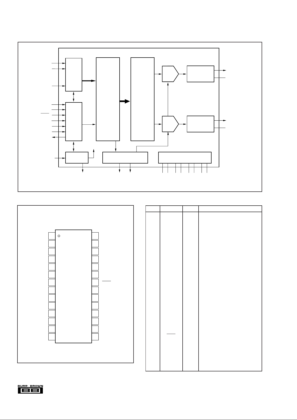
PIN CONFIGURATION
Top View SSOP
PIN NAME I/O DESCRIPTION
1 LRCK I Left/Right Word Clock
(1)
2 DATA I Data In for Left/Right Channels
(1)
3 BCLK I Bit Clock
(1)
4 CLKO O System Clock Output
5 SCLK I System Clock Input
(1)
6VSS— Digital Ground
7V
DD
— Digital Supply, +3.3V.
8 TEST1 I Test Pin
(2)
. Must be connected to
ground (V
SS
).
9 TEST2 I Test Pin
(2)
. Must be connected to
ground (V
SS
).
10 V
CC
R — Analog Supply for Right Channel, +5V
11 GNDR — Analog Ground for Right Channel
12 V
COM
R — Common for Right Channel
13 V
OUT
R O Analog Output for Right Channel
14 GNDA — Analog Ground
15 V
CC
A — Analog Supply, +5V
16 V
OUT
L O Analog Output for Left Channel
17 V
COM
L — Common for Left Channel
18 GNDL — Analog Ground for Left Channel
19 V
CC
L — Analog Supply for Left Channel, +5V
20 NC — Not Connected
21 NC — Not Connected
22 RSTB I Reset, Active Low
(2)
.
23 ZEROL O Zero Flag for Left Channel
24 ZEROR O Zero Flag for Right Channel
25 MDO O Mode Data Out
(3)
26 MDI I Mode Data In
(2)
27 MC I Mode Clock
(2)
28 ML I Mode Latch
(2)
NOTES: (1) Schmitt-Trigger input, 5V tolerant. (2) Schmitt-Trigger input with
internal pull-down, 5V tolerant. (3) Tri-state output.
PIN ASSIGNMENTS
BLOCK DIAGRAM
1
2
3
4
5
6
7
8
9
10
11
12
13
14
28
27
26
25
24
23
22
21
20
19
18
17
16
15
LRCK
DATA
BCLK
CLKO
SCLK
V
SS
V
DD
TEST1
TEST2
V
CC
R
GNDR
V
COM
R
V
OUT
R
GNDA
ML
MC
MDI
MDO
ZEROR
ZEROL
RSTB
NC
NC
V
CC
L
GNDL
V
COM
L
V
OUT
L
V
CC
A
PCM1737E
Audio
Serial
I/F
DAC
PCM1737
4x/8x
Oversampling
Digital Filter
with
Function
Controller
Enhanced
Multi-level
Delta-Sigma
Modulator
Output Amp and
Low-Pass Filter
DAC
BCLK
LRCK
DATA
Mode
Control
I/F
System Clock
Manager
Zero Detect
Power Supply
TEST1
TEST2
RSTB
ML
MC
MDI
MDO
V
OUT
L
V
COM
L
ZEROL
ZEROR
V
DD
V
SS
SCLK
System Clock
CLKO
V
CC
A
GNDA
V
CC
L
GNDL
V
CC
R
GNDR
Output Amp and
Low-Pass Filter
V
OUT
R
V
COM
R
®
5 PCM1737
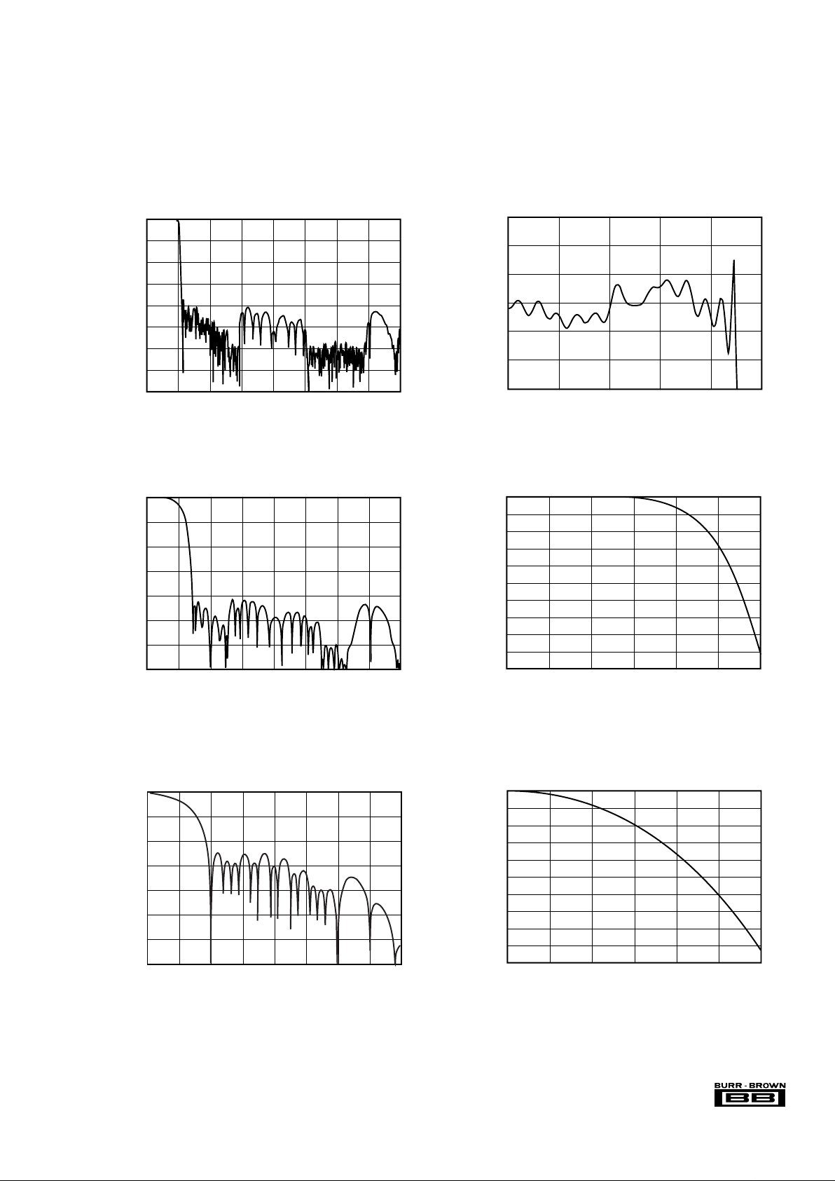
TYPICAL PERFORMANCE CURVES
All specifications at TA = +25°C, VDD = VCC = 5V, SYSCLK = 384fS (fS = 44.1kHz), and 24-bit input data, unless otherwise noted.
DIGITAL FILTER
Digital Filter (De-Emphasis Off, fS = 44.1kHz)
0 0.5 1 1.5 2 2.5 3 3.5 4
0
–20
–40
–60
–80
–100
–120
–140
–160
Amplitude (dB)
FREQUENCY RESPONSE
(Sharp Roll-Off)
Frequency (x f
S
)
PASSBAND RIPPLE
(Sharp Roll-Off)
Frequency (x f
S
)
Amplitude (dB)
0.003
0.002
0.001
0
–0.001
–0.002
–0.003
0 0.1 0.2 0.3 0.4 0.5
TRANSITION CHARACTERISTICS
(Slow Roll-Off 1)
Frequency (x f
S
)
Amplitude (dB)
0
–2
–4
–6
–8
–10
–12
–14
–16
–18
–20
0 0.1 0.2 0.3 0.4 0.5 0.6
FREQUENCY RESPONSE
(Slow Roll-Off 1)
Frequency (x f
S
)
Amplitude (dB)
0
–20
–40
–60
–80
–100
–120
–140
0 0.5 1.0 1.5 2.0 2.5 3.0 3.5 4.0
FREQUENCY RESPONSE
(Slow Roll-Off 2)
Frequency (x f
S
)
Amplitude (dB)
0
–20
–40
–60
–80
–100
–120
–140
0 0.5 1.0 1.5 2.0 2.5 3.0 3.5 4.0
TRANSITION CHARACTERISTICS
(Slow Roll-Off 2)
Frequency (x f
S
)
Amplitude (dB)
0
–1
–2
–3
–4
–5
–6
–7
–8
–9
–10
0 0.1 0.2 0.3 0.4 0.5 0.6
®
6
PCM1737
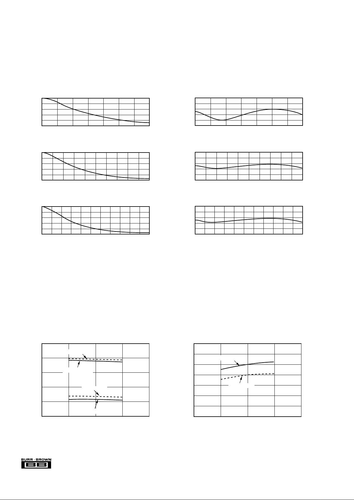
TYPICAL PERFORMANCE CURVES (Cont.)
All specifications at TA = +25°C, VDD = VCC = 5V, SYSCLK = 384fS (fS = 44.1kHz), and 24-bit input data, unless otherwise noted.
ANALOG DYNAMIC PERFORMANCE
Supply Voltage Characteristics
DIGITAL FILTER
De-Emphasis Error
DE-EMPHASIS FREQUENCY RESPONSE (fS = 32kHz)
02468101214
Frequency (kHz)
0
–2
–4
–6
–8
–10
Level (dB)
DE-EMPHASIS FREQUENCY RESPONSE (fS = 48kHz)
0246810121416182022
Frequency (kHz)
0
–2
–4
–6
–8
–10
Level (dB)
DE-EMPHASIS FREQUENCY RESPONSE (fS = 44.1kHz)
02468101214161820
Frequency (kHz)
0
–2
–4
–6
–8
–10
Level (dB)
DE-EMPHASIS ERROR (fS = 32kHz)
02468101214
Frequency (kHz)
0.5
0.3
0.1
–0.1
–0.3
–0.5
0.5
0.3
0.1
–0.1
–0.3
–0.5
0.5
0.3
0.1
–0.1
–0.3
–0.5
Level (dB)
DE-EMPHASIS ERR0R (fS = 48kHz)
0246810121416182022
Frequency (kHz)
Level (dB)
DE-EMPHASIS ERROR (fS = 44.1kHz)
02468101214161820
Frequency (kHz)
Level (dB)
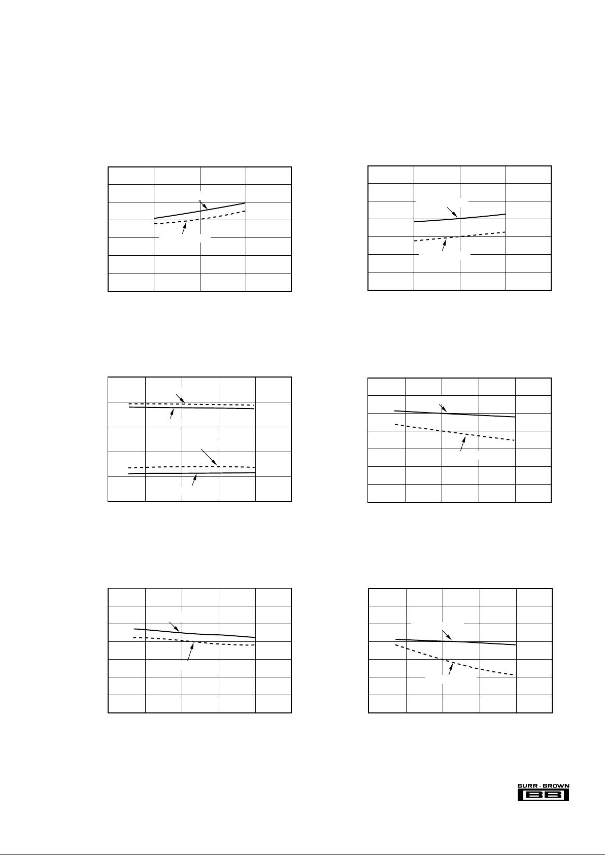
DYNAMIC RANGE vs V
CC
(VDD = 3.3V)
V
CC
(V)
Dynamic Range (dB)
110
108
106
104
102
100
98
96
4.0 4.5 5.0 5.5 6.0
192kHz, 128f
S
44.1kHz, 384f
S
TOTAL HARMONIC DISTORTION + NOISE vs V
CC
(VDD = 3.3V)
V
CC
(V)
THD+N (%)
10
1
0.1
0.01
0.001
0.0001
4.0 4.5 5.0 5.5 6.0
44.1kHz, 384f
S
44.1kHz, 384f
S
192kHz, 128f
S
–60dB
0dB
192kHz, 128f
S
®
7 PCM1737
TYPICAL PERFORMANCE CURVES (Cont.)
All specifications at TA = +25°C, VDD = VCC = 5V, SYSCLK = 384fS (fS = 44.1kHz), and 24-bit input data, unless otherwise noted.
ANALOG DYNAMIC PERFORMANCE (con.t)
Supply Voltage Characteristics
SIGNAL-TO-NOISE RATIO vs V
CC
(VDD = 3.3V)
V
CC
(V)
SNR (dB)
110
108
106
104
102
100
98
96
4.0 4.5 5.0 5.5 6.0
192kHz, 128f
S
44.1kHz, 384f
S
CHANNEL SEPARATION vs V
CC
VCC (V)
Channel Separation (dB)
110
108
106
104
102
100
98
96
4.0 4.5 5.0 5.5 6.0
192kHz, 128f
S
44.1kHz, 384f
S
Temperature Characteristics
TOTAL HARMONIC DISTORTION + NOISE
vs TEMPERATURE
V
CC
(V)
THD+N (%)
10
1
0.1
0.01
0.001
0.0001
4.0 4.5 5.0 5.5 6.0
44.1kHz, 384f
S
44.1kHz, 384f
S
192kHz, 128f
S
–60dB
0dB
192kHz, 128f
S
DYNAMIC RANGE vs TEMPERATURE
(V
DD
= 3.3V)
Temperature (°C)
Dynamic Range (dB)
110
108
106
104
102
100
98
96
–25 0 25 50 75 100
192kHz, 128f
S
44.1kHz, 384f
S
CHANNEL SEPARATION vs TEMPERATURE
(V
DD
= 3.3V)
Temperature (°C)
Channel Separation (dB)
110
108
106
104
102
100
98
96
–25 0 25 50 75 100
192kHz, 128f
S
44.1kHz, 384f
S
SIGNAL-TO-NOISE RATIO vs TEMPERATURE
(V
DD
= 3.3V)
Temperature (°C)
SNR (dB)
110
108
106
104
102
100
98
96
–25 0 25 50 10075
192kHz, 128f
S
44.1kHz, 384f
S
®
8
PCM1737
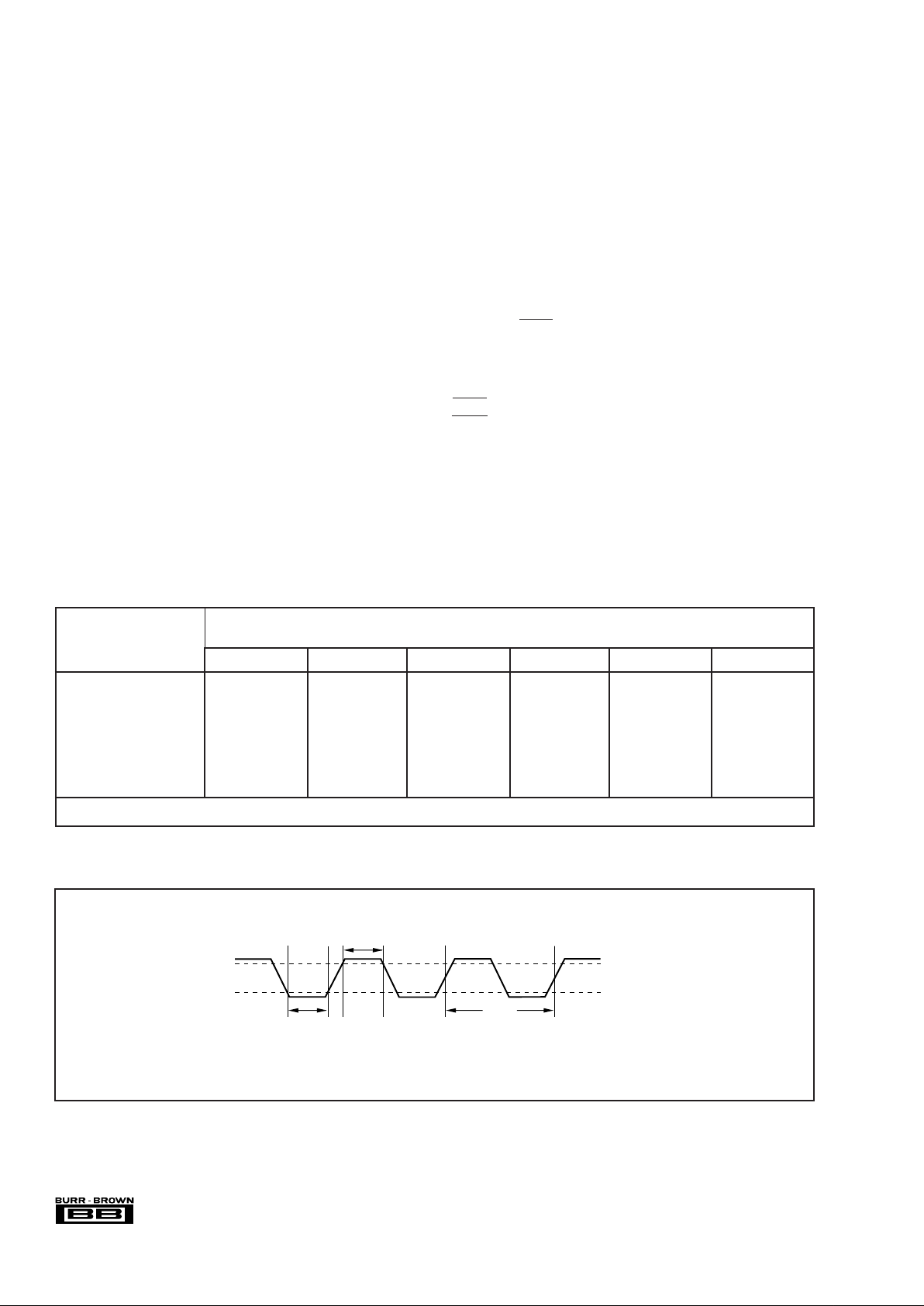
FIGURE 1. System Clock Input Timing.
SYSTEM CLOCK AND RESET
FUNCTIONS
SYSTEM CLOCK INPUT
The PCM1737 requires a system clock for operating the
digital interpolation filters and multi-level delta-sigma modulators. The system clock is applied at the SCLK input (pin 5).
Table I shows examples of system clock frequencies for
common audio sampling rates.
Figure 1 shows the timing requirements for the system clock
input. For optimal performance, it is important to use a clock
source with low phase jitter and noise. Burr-Brown’s
PLL1700 multi-clock generator is an excellent choice for
providing the PCM1737 system clock.
SYSTEM CLOCK OUTPUT
A buffered version of system clock input is available at the
CLKO output (pin 4). CLKO can operate at either full
(f
SCLK
) or half (f
SCLK
/2) rate. The CLKO output frequency
may be programmed using the CLKD bit of Control Register
20. The CLKO output pin can also be enabled or disabled
using the CLKE bit of Control Register 20. The default is
CLKO enabled.
SAMPLING FREQUENCY
(f
S
) 128f
S
192f
S
256f
S
384f
S
512f
S
768f
S
16kHz — — 4.0960 6.1440 8.1920 12.2880
32kHz — — 8.1920 12.2880 16.3840 24.5760
44.1kHz — — 11.2896 16.9344 22.5792 33.8688
48kHz — —
12.2880 18.4320 24.5760 36.8640
88.2kHz — — 22.5792 33.8688 45.1584 See Note 1
96kHz 12.2880 18.4320 24.5760 36.8640 49.1520 See Note 1
176.4kHz 22.5792 33.8688 See Note 2 See Note 2 See Note 2 See Note 2
192 24.5760 36.8640 See Note 2 See Note 2 See Note 2 See Note 2
NOTE: (1) The 768f
S
system clock rate is not supported for fS > 64kHz. (2) This system clock rate is not supported for the given sampling frequency.
TABLE I. System Clock Rates for Common Audio Sampling Frequencies.
SYSTEM CLOCK FREQUENCY (f
SCLK
)
(MHz)
POWER-ON AND EXTERNAL RESET FUNCTIONS
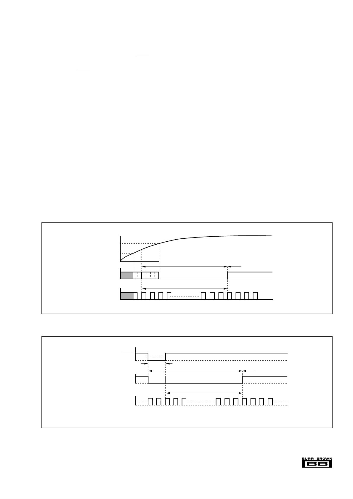
The PCM1737 includes a power-on reset function. Figure 2
shows the operation of this function. The system clock input
at SCLK should be active for at least one clock period prior
to VDD = 2.0V. With the system clock active and VDD >
2.0V, the power-on reset function will be enabled. The
initialization sequence requires 1024 system clocks from the
time VDD > 2.0V. After the initialization period, the PCM1737
will be set to its reset default state, as described in the Mode
Control Register section of this data sheet.
The PCM1737 also includes an external reset capability
using the RSTB input (pin 22). This allows an external
controller or master reset circuit to force the PCM1737 to
initialize to its reset default state.
Figure 3 shows the external reset operation and timing. The
RSTB pin is set to logic ‘0’ for a minimum of 20ns. The
RSTB pin is then set to a logic “1” state, which starts the
initialization sequence which lasts for 1024 system clock
periods. After the initialization sequence is complete, the
PCM1737 will be set to its reset default state, as described
in the Mode Control Register section of this data sheet.
t
SCLKH
t
SCLKL
f
SCLK
System Clock Pulse Width High t
SCLKH
: 7ns min
System Clock Pulse Width Low t
SCLKL
: 7ns min
2.0V
0.8V
“H”
“L”
SCLK
®
9 PCM1737
FIGURE 2. Power-On Reset Timing.
FIGURE 3. External Reset Timing.
The external reset is especially useful in applications
where there is a delay between PCM1737 power up and
system clock activation. In this case, the RSTB pin should
be held at a logic ‘0’ level until the system clock has been
activated. The RSTB pin may then be set to a logic ‘1”
state to start the initialization sequence.
AUDIO SERIAL INTERFACE
The audio serial interface for the PCM1737 is comprised of
a 3-wire synchronous serial port. It includes LRCK (pin 1),
BCLK (pin 3), and DATA (pin 2). BCLK is the serial
audio bit clock, and it is used to clock the serial data
present on DATA into the audio interface’s serial shift
register. Serial data is clocked into the PCM1737 on the
rising edge of BCLK. LRCK is the serial audio left/right
word clock. It is used to latch serial data into the serial
audio interface’s internal registers.
Both LRCK and BCLK must be synchronous to the system
clock. Ideally, it is recommended that LRCK and BCLK be
derived from the system clock input or output, SCLK or
CLKO. The left/right clock, LRCK, is operated at the
sampling frequency, fS. The bit clock, BCLK, may be
operated at 48 or 64 times the sampling frequency.
Audio Data Formats and Timing
The PCM1737 supports industry-standard audio data formats,
including standard, I2S, and left-justified. The data formats
are shown in Figure 4. Data formats are selected using the
format bits, FMT[2:0], in Control Register 20. The default
data format is 24-bit standard. All formats require Binary
Two’s Complement, MSB-first audio data. Figure 5 shows a
detailed timing diagram for the serial audio interface.
SERIAL CONTROL INTERFACE
The serial control interface is a 4-wire serial port which
operates asynchronously to the serial audio interface. The
serial control interface is utilized to program and read the onchip mode registers. The control interface includes MDO (pin
25), MDI (pin 26), MC (pin 27), and ML (pin 28). MDO is the
serial data output, used to read back the values of the mode
registers. MDI is the serial data input, used to program the
mode registers. MC is the serial bit clock, used to shift data in
and out of the control port. ML is the control port latch clock.
1024 system clocks
Reset
Reset Removal
V
CC
= V
DD
Internal Reset
2.4V
2.0V
1.6V
System Clock
(SCLK)
1024 system clocks
Reset
Reset Removal
System Clock
(SCLK)
Internal Reset
RSTB
t
RST
(1)
NOTE: (1) t
RST
= 20ns min.
 Loading...