

Burr Brown PCM1720E, PCM1720E-2K Datasheet
© 1996 Burr-Brown Corporation PDS-1333B Printed in U.S.A. August, 1996
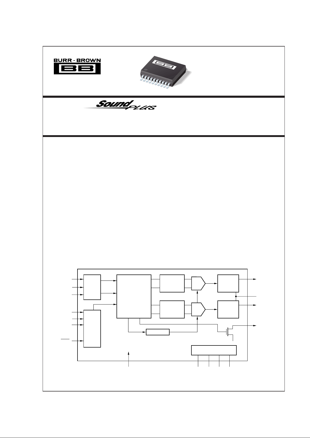
Serial
Input
I/F
Mode
Control
I/F
8X Oversampling
Digital Filter
with Function
Controller
SCKI
256f
S
/384f
S
VCCAGND
Multi-level
Delta-Sigma
Modulator
V
OUT
L
CAP
Open Drain
DAC
Multi-level
Delta-Sigma
Modulator
Low-pass
Filter
Low-pass
Filter
BPZ-Cont.
V
OUT
R
ZERO
DAC
MC
MD
ML
LRCIN
DIN
BCKIN
RSTB
Power Supply
VDDDGND
Stereo Audio
DIGITAL-TO-ANALOG CONVERTER
MPEG2/AC-3 COMPATIBLE
TM
49%
FPO
PCM1720
DESCRIPTION
The PCM1720 is a complete low cost stereo audio
digital-to-analog converter (DAC), operating off of a
256fS or 384fS system clock. The DAC contains a 3rdorder ∆Σ modulator, a digital interpolation filter, and
an analog output amplifier. The PCM1720 can accept
16-, 20-, or 24-bit input data in either normal or I
2
S
formats.
The digital filter performs an 8X interpolation func-
tion and includes selectable features such as soft mute,
digital attenuation and digital de-emphasis. The
PCM1720 can accept standard digital audio sampling
frequencies as well as one-half and double sampling
frequencies.
The PCM1720 is ideal for applications which combine
compressed audio and video data such as DVD, DVDROM, set-top boxes and MPEG sound cards.
®
FEATURES
● ACCEPTS 16-, 20-, OR 24-BIT INPUT DATA
● COMPLETE STEREO DAC: Includes Digital
Filter and Output Amp
● DYNAMIC RANGE: 96dB
● MULTIPLE SAMPLING FREQUENCIES:
16kHz to 96kHz
8X Oversampling at All Sampling
Frequencies
● SYSTEM CLOCK: 256f
S
/384f
S
● NORMAL OR I2S DATA INPUT FORMATS
● SELECTABLE FUNCTIONS:
Soft Mute
Digital Attenuator (256 Steps)
Digital De-emphasis
● OUTPUT MODE: Left, Right, Mono, Mute
International Airport Industrial Park • Mailing Address: PO Box 11400, Tucson, AZ 85734 • Street Address: 6730 S. Tucson Blvd., Tucson, AZ 85706 • Tel: (520) 746-1111 • Twx: 910-952-1111
Internet: http://www.burr-brown.com/ • FAXLine: (800) 548-6133 (US/Canada Only) • Cable: BBRCORP • Telex: 066-6491 • FAX: (520) 889-1510 • Immediate Product Info: (800) 548-6132
®
PCM1720
®
PCM1720
2
SPECIFICATIONS
All specifications at +25°C, +VCC = +V
DD
= +5V, fS = 44.1kHz, and 16-bit input data, SYSCLK = 384fS, unless otherwise noted.
PCM1720
PARAMETER CONDITIONS MIN TYP MAX UNITS
RESOLUTION 16 24 Bits
DATA FORMAT
Audio Data Format Standard/I
2
S
Data Bit Length 16/20/24
Selectable
Sampling Frequency (f
S
) Standard f
S
32 44.1 48 kHz
One-half f
S
16 22.05 24 kHz
Double f
S
64 88.2 96 kHz
Internal System Clock Frequency 256f
S
/384f
S
DIGITAL INPUT/OUTPUT LOGIC LEVEL TTL
DYNAMIC PERFORMANCE
(1)
THD+N at fS (0dB) fS = 44.1kHz –90 –80 dB
f
S
= 96kHz –88 dB
THD+N at –60dB f
S
= 44.1kHz –34 dB
f
S
= 96kHz –31 dB
Dynamic Range f
S
= 44.1kHz 90 96 dB
f
S
= 96kHz 93 dB
Signal-to-Noise Ratio
(2)
fS = 44.1kHz 92 100 dB
f
S
= 96kHz 97 dB
Channel Separation f
S
= 44.1kHz 90 97 dB
DC ACCURACY
Gain Error ±1.0 ±5.0 % of FSR
Gain Mismatch, Channel-to-Channel ±1.0 ±5.0 % of FSR
Bipolar Zero Error V
OUT
= VCC/2 at BPZ ±30 mV
ANALOG OUTPUT
Output Voltage Full Scale (0dB) 0.62 x V
CC
Vp-p
Center Voltage V
CC
/2 VDC
Load Impedance AC Load 5 kΩ
DIGITAL FILTER PERFORMANCE
Passband 0.445 f
S
Stopband 0.555 f
S
Passband Ripple ±0.17 dB
Stopband Attenuation –35 dB
Delay Time 11.125/f
S
sec
De-emphasis Error –0.2 +0.55 dB
INTERNAL ANALOG FILTER
–3dB Bandwidth 100 kHz
Passband Response f = 20kHz –0.16 dB
POWER SUPPLY REQUIREMENTS
Voltage Range V
DD
, V
CC
4.5 5 5.5 VDC
Supply Current: I
CC + IDD
VCC = VDD = 5V, fS = 44.1kHz 18 25 mA
V
CC
= VDD = 5V, fS = 96kHz 25 35 mA
TEMPERATURE RANGE
Operation –25 +85 °C
Storage –55 +100 °C
NOTES: (1) Dynamic performance specs are tested with 20kHz low pass filter and THD+N specs are tested with 30kHz LPF, 400Hz HPF, Average-Mode. (2) SNR
is tested with Infinite Zero Detection off.
The information provided herein is believed to be reliable; however, BURR-BROWN assumes no responsibility for inaccuracies or omissions. BURR-BROWN assumes
no responsibility for the use of this information, and all use of such information shall be entirely at the user’s own risk. Prices and specifications are subject to change
without notice. No patent rights or licenses to any of the circuits described herein are implied or granted to any third party. BURR-BROWN does not authorize or warrant
any BURR-BROWN product for use in life support devices and/or systems.
®
PCM1720
3
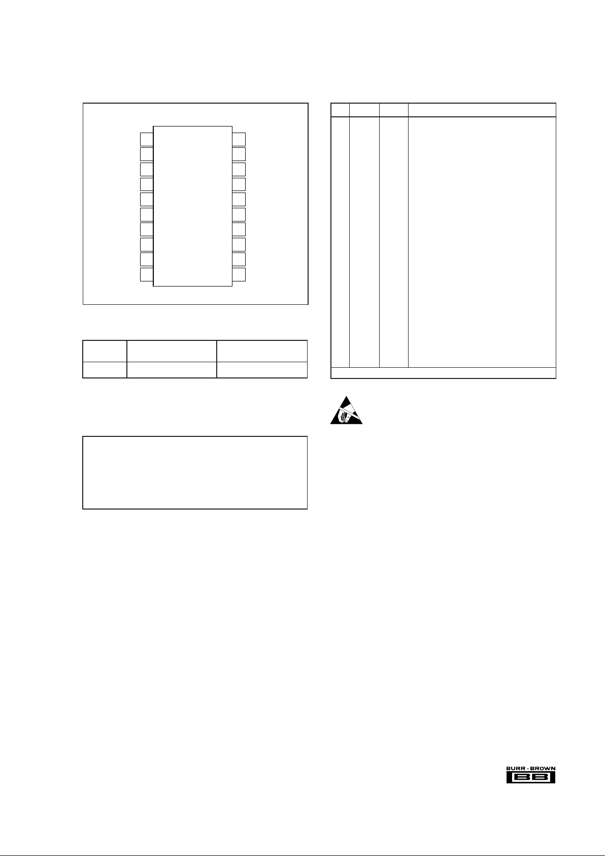
PIN ASSIGNMENTS
PIN NAME TYPE FUNCTION
1 NC — No Connection.
2 SCKI IN System Clock Input: 256f
S
or 384fS.
3 TEST OUT Reserved for Factory Use.
4* ML IN Latch Enable for Serial Control Data.
5* MC IN Clock for Serial Control Data.
6* MD IN Data Input for Serial Control.
7* RSTB IN Reset Input. When this pin is low, the digital
filters and modulators are held in reset.
8 ZERO OUT Zero Data Flag. This pin is low when the data is
continuously zero for more than 65,535 cycles of
BCKIN.
9V
OUT
R OUT Right Channel Analog Output.
10 AGND PWR Analog Ground.
11 V
CC
PWR Analog Power Supply (+5V).
12 V
OUT
L OUT Left Channel Analog Output.
13 CAP — Common Pin for Analog Output Amplifiers.
14* BCKIN IN Bit Clock for Clocking in the Audio Data.
15* DIN IN Serial Audio Data Input.
16* LRCIN IN Left/Right Word Clock. Frequency is equal to fs.
17 GND PWR Ground.
18 NC — No Connection.
19 V
DD
PWR Digital Power Supply (+5V). Recommended con-
nection is to the analog power supply.
20 DGND PWR Digital Ground. Recommended connection is to
the digital ground plane.
* These pins include internal pull-up resistors.
PIN CONFIGURATION
TOP VIEW SSOP
PACKAGE INFORMATION
PACKAGE DRAWING
PRODUCT PACKAGE NUMBER
(1)
PCM1720 20-Pin SSOP 334-1
NOTE: (1) For detailed drawing and dimension table, please see end of data
sheet, or Appendix C of Burr-Brown IC Data Book.
ABSOLUTE MAXIMUM RATINGS
Power Supply Voltage.......................................................................+6.5V
+V
CC
to +VDD Difference ................................................................... ±0.1V
Input Logic Voltage ..................................................–0.3V to (V
DD
+ 0.3V)
Power Dissipation .......................................................................... 300mW
Operating Temperature Range .........................................–25°C to +85°C
Storage Temperature...................................................... –55°C to +125°C
Lead Temperature (soldering, 5s).................................................. +260°C
Thermal Resistance,
θ
JA
..............................................................+70°C/W
NC
SCKI
TEST
ML
MC
MD
RSTB
ZERO
V
OUT
R
AGND
DGND
V
DD
NC
GND
LRCIN
DIN
BCKIN
CAP
V
OUT
L
V
CC
1
2
3
4
5
6
7
8
9
10
20
19
18
17
16
15
14
13
12
11
ELECTROSTATIC
DISCHARGE SENSITIVITY
This integrated circuit can be damaged by ESD. Burr-Brown
recommends that all integrated circuits be handled with
appropriate precautions. Failure to observe proper handling
and installation procedures can cause damage.
ESD damage can range from subtle performance degradation
to complete device failure. Precision integrated circuits may
be more susceptible to damage because very small parametric
changes could cause the device not to meet its published
specifications.
®
PCM1720
4
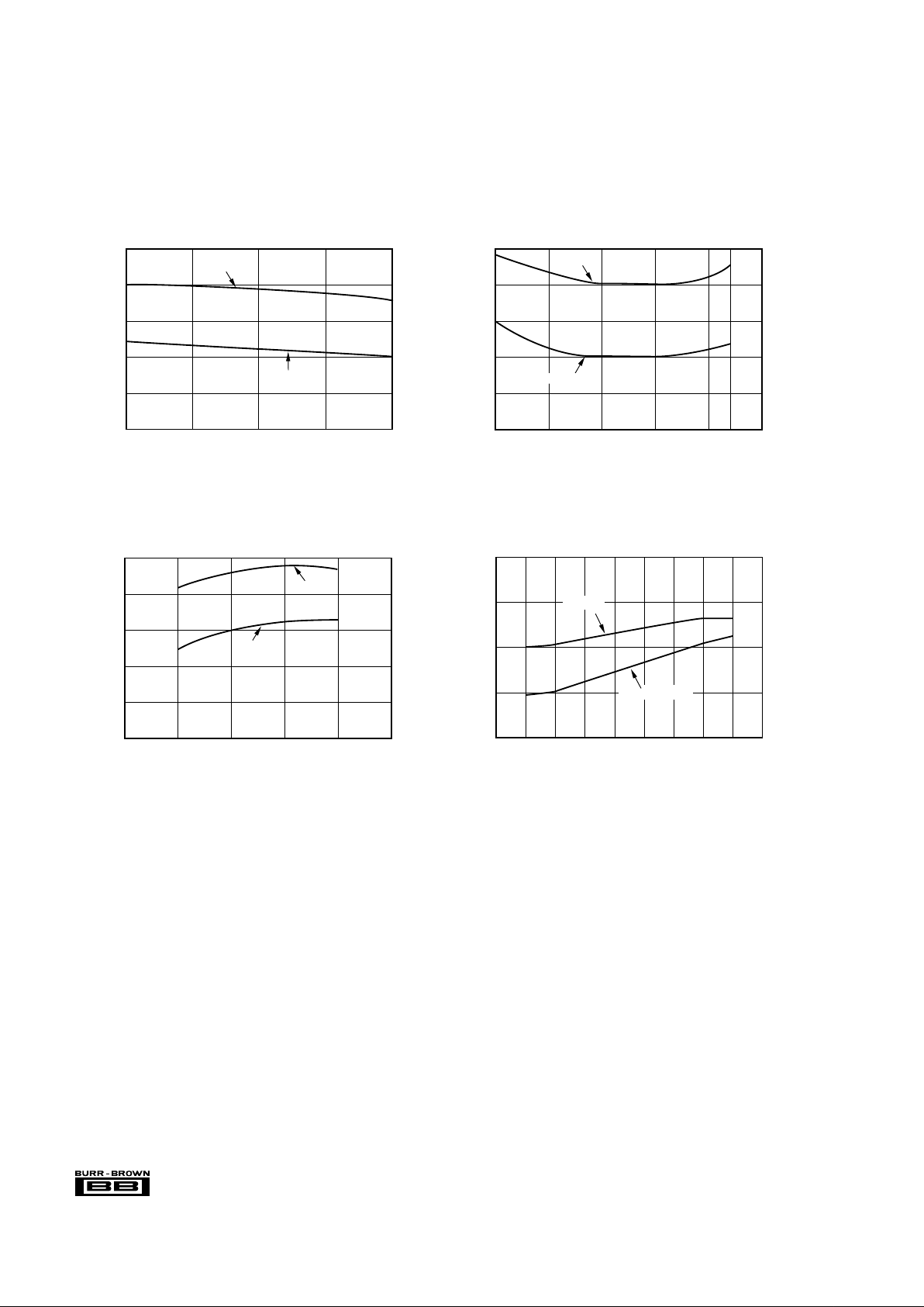
TYPICAL PERFORMANCE CURVES
At TA = +25°C, VCC = VDD = +5V, fS = 44.1kHz, 16-bit input data, unless otherwise noted. Measurement bandwidth is 20kHz
DYNAMIC PERFORMANCE
THD+N vs VCC, V
DD
VCC, VDD (V)
THD+N at FS (dB)
THD+N at –60dB (dB)
–84
–86
–88
–90
–92
–94
–30
–34
–38
4.5 5.0 5.5
f
S
= 96kHz
f
S
= 44.1kHz
DYNAMIC RANGE and SNR vs VCC, V
DD
VCC, V
DD
(dB)
100
98
96
94
92
90
3.5 4.0 4.5 5.0 5.5 6.0
SNR
Dynamic
Range
THD+N vs TEMPERATURE
Temperature (°C)
THD+N at FS (dB)
–84
–86
–88
–90
–92
–90
–25 0 25 50 75 85 100
f
S
= 96kHz
fS = 44.1kHz
THD+N and DYNAMIC RANGE vs f
S
Sampling Frequency, fS (kHz)
THD+N (dB)
Dynamic Range (dB)
–86
–88
–90
–92
–94
90
92
94
96
98
44.1 48 88.2 96
Dynamic Range
THD+N
 Loading...