

Burr Brown PCM1716E, PCM1716E-2K Datasheet
Serial
Input
I/F
Mode
Control
I/F
8X Oversampling
Digital Filter with
Function
Controller
Crystal/OSC
XTI
SCK
XTO CLKO V
CC1
AGND1 VDDDGND
Enhanced
Multi-level
Delta-Sigma
Modulator
V
OUT
L
V
CC2
L
V
CC2
R
AGND2L
AGND2L
EXTL
Open Drain
DAC
Low-pass
Filter
Low-pass
Filter
BPZ-Cont.
V
OUT
R
EXTR
ZERO
DAC
MC/DM1
ML/IIS
LRCIN
DIN
BCKIN
CS/IWO
MD/DM0
MODE
MUTE
RST
Power Supply
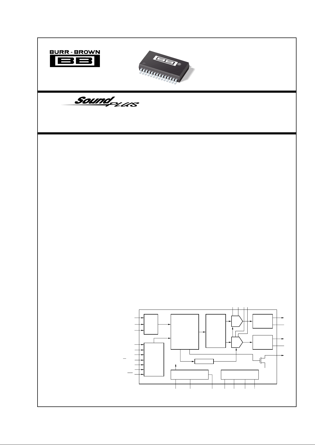
24-Bit, 96kHz Sampling
CMOS Delta-Sigma Stereo Audio
DIGITAL-TO-ANALOG CONVERTER
49%
FPO
International Airport Industrial Park • Mailing Address: PO Box 11400, Tucson, AZ 85734 • Street Address: 6730 S. Tucson Blvd., Tucson, AZ 85706 • Tel: (520) 746-1111 • Twx: 910-952-1111
Internet: http://www.burr-brown.com/ • FAXLine: (800) 548-6133 (US/Canada Only) • Cable: BBRCORP • Telex: 066-6491 • FAX: (520) 889-1510 • Immediate Product Info: (800) 548-6132
PCM1716
®
TM
DESCRIPTION
The PCM1716 is designed for Mid to High grade
Digital Audio applications which achieve 96kHz sampling rates with 24-bit audio data. PCM1716 uses a
newly developed, enhanced multi-level delta-sigma
modulator architecture that improves audio dynamic
performance and reduces jitter sensitivity in actual
applications.
The internal digital filter operates at 8x over sampling
at a 96kHz sampling rate, with two kinds of roll-off
performances that can be selected: sharp roll-off, or
slow roll-off, as required for specific applications.
PCM1716 is suitable for Mid to High grade audio
applications such as CD, DVD-Audio, and Music
Instruments, since the device has superior audio
dynamic performance, 24-bit resolution and 96kHz
sampling.
FEATURES
● ENHANCED MULTI-LEVEL DELTA-SIGMA DAC
● SAMPLING FREQUENCY (fs): 16kHz - 96kHz
● INPUT AUDIO DATA WORD:
16-, 20-, 24-Bit
● HIGH PERFORMANCE:
THD+N: –96dB
Dynamic Range: 106dB
SNR: 106dB
Analog Output Range: 0.62 x VCC (Vp-p)
● 8x OVERSAMPLING DIGITAL FILTER:
Stop Band Attenuation: –82dB
Passband Ripple: ±0.002dB
Slow Roll Off
● MULTI FUNCTIONS:
Digital De-emphasis
L/R Independent Digital Attenuation
Soft Mute
Zero Detect Mute
Zero Flag
Chip Select
Reversible Output Phase
● +5V SINGLE SUPPLY OPERATION
● SMALL 28-LEAD SSOP PACKAGE
© 1997 Burr-Brown Corporation PDS-1415C Printed in U.S.A. August, 1998
PCM1716
®
2
PCM1716
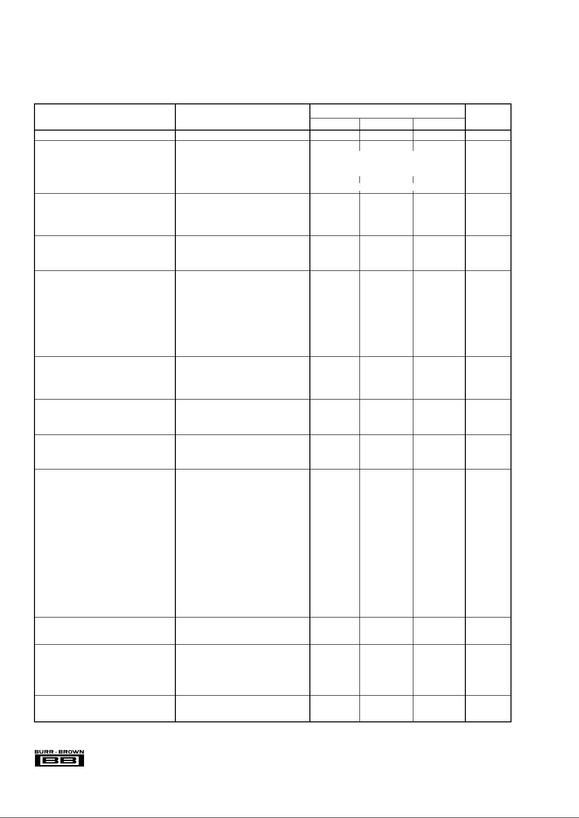
SPECIFICATIONS
All specifications at +25°C, +VCC = +V
DD
= +5V, fS = 44.1kHz, and 24-bit input data, SYSCLK = 384fS, unless otherwise noted.
PCM1716
PARAMETER CONDITIONS MIN TYP MAX UNITS
RESOLUTION 24 Bits
DATA FORMAT
Audio Data Interface Format Standard/I2S
Data Bit Length 16/20/24 Selectable
Audio Data Format MSB First, 2’s Comp
Sampling Frequency (f
S
) 16 96 kHz
System Clock Frequency
(1)
256/384/512/768f
S
DIGITAL INPUT/OUTPUT LOGIC LEVEL
Input Logic Level V
IH
2.0 V
V
IL
0.8 V
Output Logic Level (CLKO) V
OH
I
OH
= 2mA 4.5 V
V
OL
I
OL
= 4mA 0.5 V
CLKO PERFORMANCE
(2)
Output Rise Time 20 ~ 80% VDD, 10pF 5.5 ns
Output Fall Time 80 ~ 20% V
DD
, 10pF 4 ns
Output Duty Cycle 10pF Load 37 %
DYNAMIC PERFORMANCE
(3)
(24-Bit Data)
THD+N V
O
= 0dB fS = 44.1kHz –97 –90 dB
fS = 96kHz –94 dB
V
O
= –60dB fS = 44.1kHz –42 dB
Dynamic Range f
S
=44.1kHz EIAJ A-weighted 98 106 dB
f
S
= 96kHz A-weighted 103 dB
Signal-to-Noise Ratio
(4)
fS =44.1kHz EIAJ A-weighted 98 106 dB
f
S
= 96kHz A-weighted 103 dB
Channel Separation fS = 44.1kHz 96 102 dB
f
S
= 96kHz 101 dB
DYNAMIC PERFORMANCE
(3)
(16-Bit Data)
THD+N V
O
= 0dB fS = 44.1kHz –94 dB
f
S
= 96kHz –92 dB
Dynamic Range f
S
= 44.1kHz EIAJ A-weighted 98 dB
fS = 96kHz A-weighted 97 dB
DC ACCURACY
Gain Error ±1.0 ±3.0 % of FSR
Gain Mismatch: Channel-to-Channel ±1.0 ±3.0 % of FSR
Bipolar Zero Error V
O
= 0.5VCC at Bipolar Zero ±30 ±60 mV
ANALOG OUTPUT
Output Voltage Full Scale (0dB) 0.62 V
CC
Vp-p
Center Voltage 0.5 V
CC
V
Load Impedance AC Load 5 kΩ
DIGITAL FILTER PERFORMANCE
Filter Characteristics 1
(Sharp Roll-Off)
Passband ±0.002dB 0.454f
S
–3dB 0.490f
S
Stopband 0.546f
S
Passband Ripple ±0.002 dB
Stopband Attenuation Stop Band = 0.546f
S
–75 dB
Stop Band = 0.567f
S
–82 dB
Filter Characteristics 2
(Slow Roll-Off)
Passband ±0.002dB 0.274f
S
–3dB 0.454f
S
Stopband 0.732f
S
Passband Ripple ±0.002 dB
Stopband Attenuation Stopband = 0.732f
S
–82 dB
Delay Time 30/f
S
sec
De-emphasis Error ±0.1 dB
INTERNAL ANALOG FILTER
–3dB Bandwidth 100 kHz
Passband Response f = 20kHz –0.16 dB
POWER SUPPLY REQUIREMENTS
Voltage Range V
DD, VCC
4.5 5 5.5 VDC
Supply Current: I
CC +IDD
fS = 44.1kHz 32 45 mA
f
S
= 96kHz 45 mA
Power Dissipation f
S
= 44.1kHz 160 225 mW
f
S
= 96kHz 225 mW
TEMPERATURE RANGE
Operation –25 +85 °C
Storage –55 +100 °C
NOTES: (1) Refer section of system clock. (2) External buffer is recommended. (3) Dynamic performance specs are tested with 20kHz low pass filter and THD+N
specs are tested with 30kHz LPF, 400Hz HPF, Average Mode. (4) SNR is tested at internally infinity zero detection off.
®
3 PCM1716
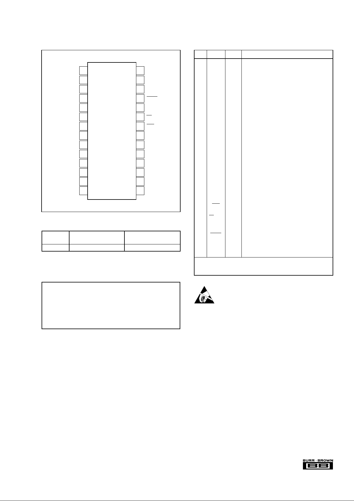
PIN NAME I/O DESCRIPTION
1 LRCIN IN Left and Right Clock Input. This clock is equal to
the sampling rate - fS.
(1)
2 DIN IN Serial Audio Data Input
(1)
3 BCKIN IN Bit Clock Input for Serial Audio Data.
(1)
4 CLKO OUT Buffered Output of Oscillator. Equivalent to
System Clock.
5 XTI IN Oscillator Input (External Clock Input)
6 XTO OUT Oscillator Output
7 DGND — Digital Ground
8V
DD
— Digital Power +5V
9V
CC
2R — Analog Power +5V
10 AGND2R — Analog Ground
11 EXTR OUT Rch, Common Pin of Analog Output Amp
12 NC — No Connection
13 V
OUT
R OUT Rch, Analog Voltage Output of Audio Signal
14 AGND1 — Analog Ground
15 V
CC
1 — Analog Power +5V
16 V
OUT
L OUT Lch, Analog Voltage Output of Audio Signal
17 NC — No Connection
18 EXTL OUT Lch, Common Pin of Analog Output Amp
19 AGND2L — Analog Ground
20 V
CC
2L — Analog Power +5V
21 ZERO OUT Zero Data Flag
22 RST IN Reset. When this pin is low, the DF and
modulators are held in reset.
(2)
23 CS/IWO IN Chip Select/Input Format Selection. When this
pin is low, the Mode Control is effective.
(3)
24 MODE IN
Mode Control Select. (H: Software, L: Hardware)
(2)
25 MUTE IN Mute Control
26 MD/DM0 IN Mode Control, DATA/De-emphasis Selection 1
(2)
27 MC/DM1 IN Mode Control, BCK/De-emphasis Selection 2
(2)
28 ML/I2S IN Mode Control, WDCK/Input Format Selection
(2)
NOTES: (1) Pins 1, 2, 3; Schmitt Trigger input. (2) Pins 22, 24, 25, 26, 27,
28; Schmitt Trigger input with pull-up resister. (3) Pin 23; Schmitt Trigger
input with pull-down resister.
PIN ASSIGNMENTSPIN CONFIGURATION
LRCIN
DIN
BCKIN
CLKO
XTI
XTO
DGND
V
DD
VCC2R
AGND2R
EXTR
NC
V
OUT
R
AGND1
ML/IIS
MC/DM1
MD/DM0
MUTE
MODE
CS/IWO
RST
ZERO
V
CC
2L
AGND2L
EXTL
NC
V
OUT
L
V
CC
1
1
2
3
4
5
6
7
8
9
10
11
12
13
14
28
27
26
25
24
23
22
21
20
19
18
17
16
15
PCM1716E
PACKAGE DRAWING
PRODUCT PACKAGE NUMBER
(1)
PCM1716E 28-Pin SSOP 324
NOTE: (1) For detailed drawing and dimension table, please see end of data
sheet, or Appendix C of Burr-Brown IC Data Book.
PACKAGE INFORMATION
ELECTROSTATIC
DISCHARGE SENSITIVITY
This integrated circuit can be damaged by ESD. Burr-Brown
recommends that all integrated circuits be handled with
appropriate precautions. Failure to observe proper handling
and installation procedures can cause damage.
ESD damage can range from subtle performance degradation
to complete device failure. Precision integrated circuits may
be more susceptible to damage because very small parametric
changes could cause the device not to meet its published
specifications.
Power Supply Voltage ...................................................................... +6.5V
+V
CC
to +VDD Difference ................................................................... ±0.1V
Input Logic Voltage .................................................. –0.3V to (V
DD
+ 0.3V)
Input Current (except power supply)............................................... ±10mA
Power Dissipation .......................................................................... 400mW
Operating Temperature Range ......................................... –25°C to +85°C
Storage Temperature...................................................... –55°C to +125°C
Lead Temperature (soldering, 5s)................................................. +260°C
ABSOLUTE MAXIMUM RATINGS
The information provided herein is believed to be reliable; however, BURR-BROWN assumes no responsibility for inaccuracies or omissions. BURR-BROWN assumes
no responsibility for the use of this information, and all use of such information shall be entirely at the user’s own risk. Prices and specifications are subject to change
without notice. No patent rights or licenses to any of the circuits described herein are implied or granted to any third party. BURR-BROWN does not authorize or warrant
any BURR-BROWN product for use in life support devices and/or systems.
®
4
PCM1716
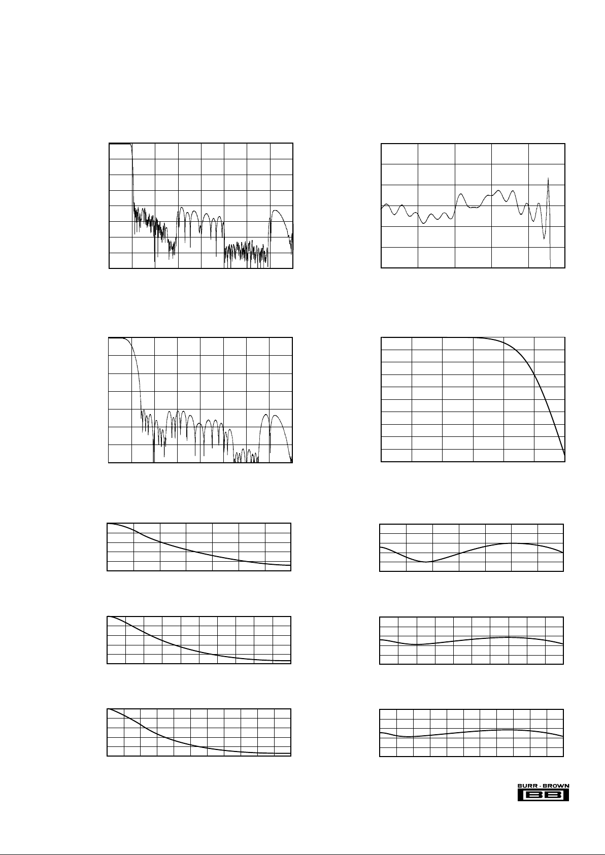
–60dB OUTPUT SPECTRUM
(f = 1kHz, f
S
= 44.1kHz, 24-Bit Data)
Frequency (Hz)
Amplitude (dB)
–60
–70
–80
–90
–100
–110
–120
–130
–140
–150
202468101214161820
–60dB OUTPUT SPECTRUM
(f = 1kHz, f
S
= 44.1kHz, 16-Bit Data)
Frequency (Hz)
Amplitude (dB)
–60
–70
–80
–90
–100
–110
–120
–130
–140
–150
202468101214161820
TYPICAL PERFORMANCE CURVES
All specifications at +25°C, +VCC = +V
DD
= +5V, fS = 44.1kHz, and 24-bit input data, SYSCLK = 384fS, unless otherwise noted.
THD+N vs SAMPLING FREQUENCY
(V
CC
= VDD = 5V, 24-Bit)
Sampling Frequency f
S
(kHz)
THD+N at F/S (dB)
88
91
94
97
100
103
32 44.1 48 96
256fs
384fs
DYNAMIC RANGE vs SAMPLING FREQUENCY
(V
CC
= VDD = 5V, 24-Bit)
Sampling Frequency f
S
(kHz)
Dynamic Range (A-weighted) (dB)
110
108
106
104
102
100
32 44.1 48 96
256/384f
S
THD+N vs LEVEL
(f
S
= 44.1kHz)
Amplitude (dB)
THD+N (%)
10
1
0.1
0.010
0.001
THD+N (dB)
–20
–40
–60
–80
–100
–30
–50
–70
–90
–50–60 –40 –30 –20 –10 0
16-Bit
24-Bit
SNR vs SAMPLING FREQUENCY
(V
CC
= VDD = 5V, 24-Bit)
Sampling Frequency f
S
(kHz)
SNR (A-weighted) (dB)
110
108
106
104
102
100
32 44.1 48 96
256/384f
S
®
5 PCM1716
0 0.5 1.51 2.52 3.534
0
–20
–40
–60
–80
–100
–120
–140
Amplitude (dB)
OVERALL FREQUENCY CHARACTERISTIC
(Slow Roll-Off)
Frequency (x f
S
)
0 0.5 1 1.5 2 2.5 3 3.5 4
0
–20
–40
–60
–80
–100
–120
–140
–160
Amplitude (dB)
OVERALL FREQUENCY CHARACTERISTIC
(Sharp Roll-Off)
Frequency (x f
S
)
TYPICAL PERFORMANCE CURVES (CONT)
0 0.1 0.2 0.3 0.4 0.5 0.6
0
–2
–4
–6
–8
–10
–12
–14
–16
–18
–20
Amplitude (dB)
FREQUENCY CHARACTERISTIC
(Slow Roll-Off)
Frequency (x f
S
)
0 0.1 0.2 0.3 0.4 0.5
0.003
0.002
0.001
0
–0.001
–0.002
–0.003
Amplitude (dB)
PASSBAND RIPPLE CHARACTERISTIC
(Sharp Roll-Off)
Frequency (x f
S
)
DE-EMPHASIS FREQUENCY RESPONSE (fS = 32kHz)
02468101214
Frequency (kHz)
0
–2
–4
–6
–8
–10
Level (dB)
DE-EMPHASIS FREQUENCY RESPONSE (fS = 48kHz)
0246810121416182022
Frequency (kHz)
0
–2
–4
–6
–8
–10
Level (dB)
DE-EMPHASIS FREQUENCY RESPONSE (fS = 44.1kHz)
02468101214161820
Frequency (kHz)
0
–2
–4
–6
–8
–10
Level (dB)
DE-EMPHASIS ERROR (fS = 32kHz)
02468101214
Frequency (kHz)
0.5
0.3
0.1
–0.1
–0.3
–0.5
0.5
0.3
0.1
–0.1
–0.3
–0.5
0.5
0.3
0.1
–0.1
–0.3
–0.5
Level (dB)
DE-EMPHASIS ERR0R (fS = 48kHz)
0246810121416182022
Frequency (kHz)
Level (dB)
DE-EMPHASIS ERROR (fS = 44.1kHz)
02468101214161820
Frequency (kHz)
Level (dB)
 Loading...