

Burr Brown OPA2631U-2K5, OPA2631U Datasheet
®
OPA2631
I
nternational Airport Industrial Park • Mailing Address: PO Box 11400, Tucson, AZ 85734 • Street Address: 6730 S. Tucson Blvd., Tucson, AZ 85706 • Tel: (520) 746-1111
Twx: 910-952-1111 • Internet: http://www.burr-brown.com/ • Cable: BBRCORP • Telex: 066-6491 • FAX: (520) 889-1510 • Immediate Product Info: (800) 548-6132
FEATURES
● HIGH BANDWIDTH: 75MHz (G = +2)
● LOW SUPPLY CURRENT: 6mA/ch
● +3V AND +5V OPERATION
● INPUT RANGE INCLUDES GROUND
● 4.8V OUTPUT SWING ON +5V SUPPLY
● HIGH SLEW RATE: 100V/µs
● LOW INPUT VOLTAGE NOISE: 6nV/√Hz
© 1999 Burr-Brown Corporation PDS-1378A Printed in U.S.A. August, 1999
Dual, Low Power , Single-Supply
OPERATIONAL AMPLIFIER
APPLICATIONS
● DIFFERENTIAL RECEIVERS/DRIVERS
● ACTIVE FILTERS
● MATCHED I AND Q CHANNEL AMPLIFIERS
● CCD IMAGING CHANNELS
● LOW POWER ULTRASOUND
● PORTABLE CONSUMER ELECTRONICS
TM
DESCRIPTION
The OPA2631 is a dual, low power, voltage-feedback
amplifier designed to operate on a single +3V or +5V
supply. Operation on ±5V or +10V supplies is also
supported. The input range extends below ground and
to within 1V of the positive supply. Using complementary common-emitter outputs provides an output swing
to within 30mV of ground and 130mV of the positive
supply. The high output drive current and low differential gain and phase errors also make it ideal for singlesupply consumer video products.
Low distortion operation is ensured by the high gain
bandwidth (68MHz) and slew rate (100V/µs), making
the OPA2631 an ideal input buffer stage to 3V and 5V
CMOS converters. Unlike other low power, singlesupply amplifiers, distortion performance improves as
the signal swing is decreased. A low 6nV/√Hz input
voltage noise supports wide dynamic range operation.
The OPA2631 is available in an industry standard
SO-8 package. Where a single channel, single-supply
operational amplifier is required, consider the OPA631
and OPA632. Where higher full-power bandwidth and
lower distortion are required, consider the OPA2634.
SINGLES DUALS
Medium Speed, No Disable OPA631 OPA2631
With Disable OPA632 —
High Speed, No Disable OPA634 OPA2634
With Disable OPA635 —
RELATED PRODUCTS
OPA2631
For most current data sheet and other product
information, visit www.burr-brown.com
SPICE model available at www.burr-brown.com
1/2
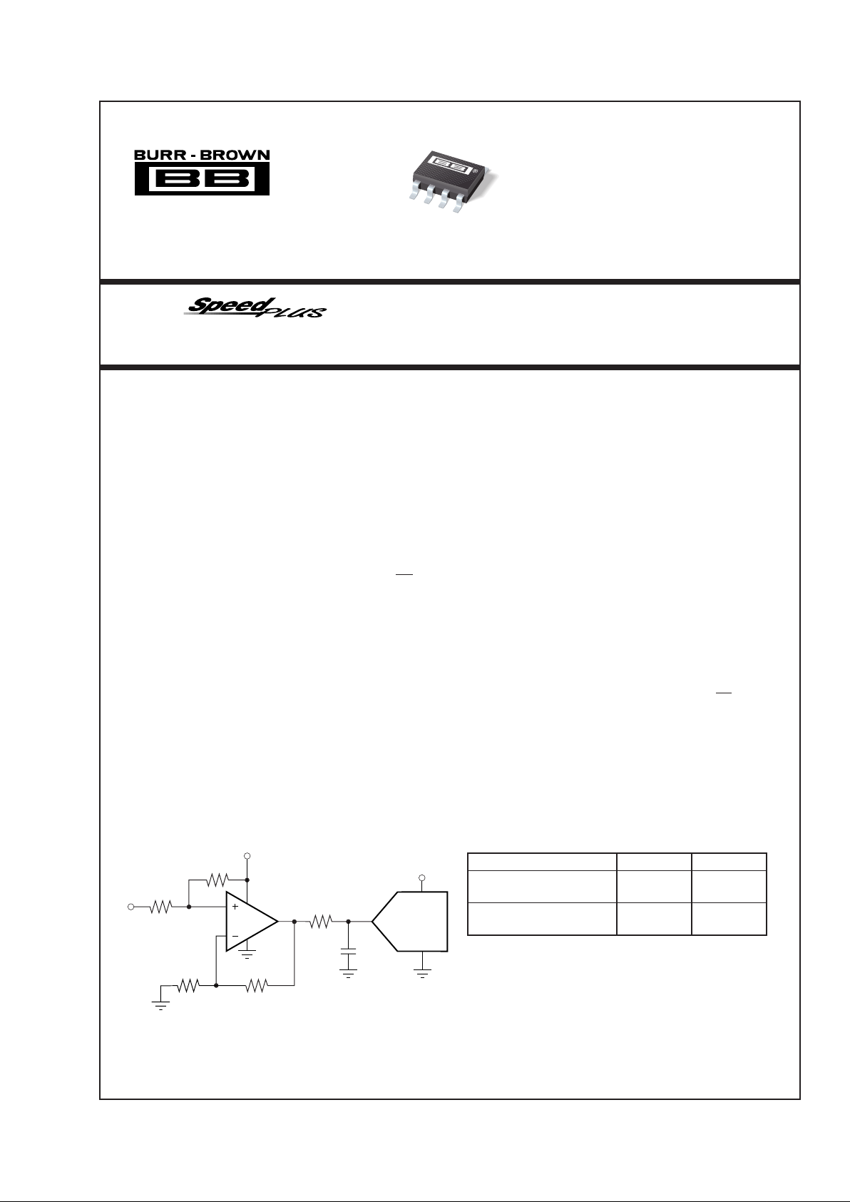
OPA2631
V
IN
750Ω562Ω
2.26kΩ
374Ω
22pF
+3V
100Ω
+3V
ADS901
10-Bit
20Msps
2
®
OPA2631
OPA2631U
TYP GUARANTEED
0°C to –40°C to
MIN/
TEST
PARAMETER CONDITIONS +25°C +25°C70°C +85°C UNITS MAX
LEVEL
(1)
SPECIFICATIONS: VS = +5V
At TA = 25°C, G = +2, RF = 750Ω, and RL = 150Ω to VS/2, unless otherwise noted.
AC PERFORMANCE (Figure 1)
Small-Signal Bandwidth G = +2, V
O
≤ 0.5Vp-p 75 50 40 32 MHz min B
G = +5, V
O
≤ 0.5Vp-p 16 12 10 8.5 MHz min B
G = +10, V
O
≤ 0.5Vp-p 7.6 5.6 4.2 3.7 MHz min B
Gain Bandwidth Product G ≥ +10 68 51 40 36 MHz min B
Peaking at a Gain of +1 V
O
≤ 0.5Vp-p 5 — — — dB typ C
Slew Rate G = +2, 2V Step 100 64 52 47 V/µs min B
Rise Time 0.5V Step 5.3 8.0 11 12.8 ns max B
Fall Time 0.5V Step 5.4 7.5 10 11.6 ns max B
Settling Time to 0.1% G = +2, 1V Step 17 28 38 42 ns max B
Spurious Free Dynamic Range V
O
= 2Vp-p, f = 5MHz 44 40 38 35 dB min B
V
O
= 2Vp-p, f = 1MHz, RL = 1kΩ 84 68 66 62 dB min B
Input Voltage Noise f > 1MHz 6.0 6.8 7.6 7.9 nV/√Hz max B
Input Current Noise f > 1MHz 1.9 2.6 2.9 3.6 pA/√Hz max B
NTSC Differential Gain 0.5 — — — % typ C
NTSC Differential Phase 1.2 — — — degrees typ C
Channel-to-Channel Isolation Input Referred, f = 5MHz 93 — — — dB typ C
DC PERFORMANCE
Open-Loop Voltage Gain 62 56 50 46 dB min A
Input Offset Voltage 2.5 6 8 11 mV max A
Average Offset Voltage Drift — — — 50 µV/°C max B
Input Bias Current V
CM
= 2.0V 11 21 27 40 µA max A
Input Offset Current V
CM
= 2.0V 0.3 1 1.3 2 µA max A
Input Offset Current Drift — — — 7 nA/°C max B
INPUT
Least Positive Input Voltage –0.5 –0.1 –0.1 –0.1 V max B
Most Positive Input Voltage 4.0 3.7 3.7 3.5 V min A
Common-Mode Rejection Ratio (CMRR)
Input Referred 74 70 68 60 dB min A
Input Impedance
Differential-Mode 10 || 2.1 — — — kΩ || pF typ C
Common-Mode 400 || 1.2 — — — kΩ || pF typ C
OUTPUT
Least Positive Output Voltage R
L
= 1kΩ to 2.5V 0.03 0.06 0.09 0.12 V max A
R
L
= 150Ω to 2.5V 0.16 0.17 0.20 1.7 V max A
Most Positive Output Voltage R
L
= 1kΩ to 2.5V 4.87 4.8 4.7 4.6 V min A
R
L
= 150Ω to 2.5V 4.60 4.4 4.4 3.1 V min A
Current Output, Sourcing 80 25 20 5 mA min A
Current Output, Sinking 90 38 24 10 mA min A
Short-Circuit Current (output shorted to either supply)
100 — — — mA typ C
Closed-Loop Output Impedance Figure 1, f ≤ 50kHz 0.6 — — — Ω typ C
POWER SUPPLY
Minimum Operating Voltage — 2.7 2.7 2.7 V min A
Maximum Operating Voltage — 10.5 10.5 10.5 V max A
Maximum Quiescent Current V
S
= +5V 6 6.4 6.7 6.9
mA/chan
max A
Minimum Quiescent Current V
S
= +5V 6 5.8 5.5 4.8
mA/chan
min A
Power Supply Rejection Ratio (PSRR) Input Referred 59 52 49 48 dB min A
THERMAL CHARACTERISTICS
Specification: U
–40 to +85
———°C typ C
Thermal Resistance
U SO-8 125 — — — °C/W typ C
NOTE: (1) Test Levels: (A) 100% tested at 25°C. Over temperature limits by characterization and simulation. (B) Limits set by characterization and simulation.
(C) Typical value only for information.
3
®
OPA2631
SPECIFICATIONS: VS = +3V
At TA = 25°C, G = +2, RF = 750Ω, and RL = 150Ω to VS/2, unless otherwise noted.
The information provided herein is believed to be reliable; however, BURR-BROWN assumes no responsibility for inaccuracies or omissions. BURR-BROWN assumes no responsibility
for the use of this information, and all use of such information shall be entirely at the user’s own risk. Prices and specifications are subject to change without notice. No patent rights or
licenses to any of the circuits described herein are implied or granted to any third party. BURR-BROWN does not authorize or warrant any BURR-BROWN product for use in life support
devices and/or systems.
OPA2631U
TYP GUARANTEED
0°C to
MIN/ TEST
PARAMETER CONDITIONS +25
°C +25°C70°C UNITS MAX
LEVEL
(1)
AC PERFORMANCE (Figure 2)
Small-Signal Bandwidth G = +2, V
O
≤ 0.5Vp-p 61 45 35 MHz min B
G = +5, V
O
≤ 0.5Vp-p 15 11 9 MHz min B
G = +10, V
O
≤ 0.5Vp-p 7.7 4.6 4.0 MHz min B
Gain Bandwidth Product G ≥ +10 63 47 34 MHz min B
Peaking at a Gain of +1 V
O
≤ 0.5Vp-p 5 — — dB typ C
Slew Rate 1V Step 95 52 46 V/µs min B
Rise Time 0.5V Step 5.6 9 11.3 ns max B
Fall Time 0.5V Step 5.6 9 11.3 ns max B
Settling Time to 0.1% 1V Step 40 63 85 ns max B
Spurious Free Dynamic Range V
O
= 1Vp-p, f = 5MHz 44 37 34 dB min B
V
O
= 1Vp-p, f = 1MHz, RL = 1kΩ 846765dB min B
Input Voltage Noise f > 1MHz 6.2 7.0 7.8 nV/√Hz max B
Input Current Noise f > 1MHz 2.0 2.6 2.9 pA/√Hz max B
Channel-to-Channel Isolation Input Reference, f = 5MHz 93 — — dB typ C
DC PERFORMANCE
Open-Loop Voltage Gain 60 54 50 dB min A
Input Offset Voltage 0.5 3.5 4 mV max A
Average Offset Voltage Drift ——45µV/°C max B
Input Bias Current V
CM
= 1.0V 12 21 26 µA max A
Input Offset Current V
CM
= 1.0V 0.3 1 1.3 µA max A
Input Offset Current Drift — — 2 nA/°C max B
INPUT
Least Positive Input Voltage –0.5 –0.3 –0.1 V max B
Most Positive Input Voltage 2 1.75 1.3 V min A
Common-Mode Rejection Ratio (CMRR) Input Referred 72 66 65 dB min A
Input Impedance
Differential-Mode 10 || 2.1 — — kΩ || pF typ C
Common-Mode 400 || 1.2 — — kΩ || pF typ C
OUTPUT
Least Positive Output Voltage R
L
= 1kΩ to 1.5V 0.03 0.05 0.05 V max A
R
L
= 150Ω to 1.5V 0.05 0.15 0.16 V max A
Most Positive Output Voltage R
L
= 1kΩ to 1.5V 2.95 2.85 2.84 V min A
R
L
= 150Ω to 1.5V 2.85 2.66 2.60 V min A
Current Output, Sourcing 55 21 14 mA min A
Current Output, Sinking 55 21 14 mA min A
Short Circuit Current (output shorted to either supply) 80 — — mA typ C
Closed-Loop Output Impedance Figure 2, f < 50kHz 0.6 — — Ω typ C
POWER SUPPLY
Minimum Operating Voltage — 2.7 2.7 V min A
Maximum Operating Voltage — 10.5 10.5 V max A
Maximum Quiescent Current V
S
= +3V 5.3 5.7 6.2
mA/chan
max A
Minimum Quiescent Current V
S
= +3V 5.3 5.0 4.8
mA/chan
min A
Power Supply Rejection Ratio (PSRR) Input Referred 57 50 48 dB min A
THERMAL CHARACTERISTICS
Specification: U
–40 to +85
°C typ C
Thermal Resistance
U SO-8 125 °C/W typ C
NOTE: (1) Test Levels: (A) 100% tested at 25°C. Over temperature limits by characterization and simulation. (B) Limits set by characterization and simulation.
(C) Typical value only for information.
4
®
OPA2631
PIN CONFIGURATIONS
Top View SO-8
1
2
3
4
8
7
6
5
+V
S
Out B
–In B
+In B
Out A
–In A
+In A
GND
OPA2631
ABSOLUTE MAXIMUM RATINGS
Power Supply ................................................................................ +11V
DC
Internal Power Dissipation ....................................See Thermal Analysis
Differential Input Voltage .................................................................. ±1.2V
Input Voltage Range .................................................... –0.5 to +V
S
+0.3V
Storage Temperature Range ......................................... –40°C to +125°C
Lead Temperature (soldering, 10s) .............................................. +300°C
Junction Temperature (T
J
) ........................................................... +175°C
ELECTROSTATIC
DISCHARGE SENSITIVITY
Electrostatic discharge can cause damage ranging from performance degradation to complete device failure. Burr-Brown Corporation recommends that all integrated circuits be handled and stored
using appropriate ESD protection methods.
ESD damage can range from subtle performance degradation to
complete device failure. Precision integrated circuits may be more
susceptible to damage because very small parametric changes
could cause the device not to meet published specifications.
PACKAGE SPECIFIED
DRAWING TEMPERATURE PACKAGE ORDERING TRANSPORT
PRODUCT PACKAGE NUMBER
(1)
RANGE MARKING NUMBER
(2)
MEDIA
OPA2631U SO-8 Surface-Mount 182 –40°C to +85°C OPA2631 OPA2631U Rails
"""""OPA2631U/2K5 Tape and Reel
NOTES: (1) For detailed drawing and dimension table, please see end of data sheet, or Appendix C of Burr-Brown IC Data Book. (2) Models with a slash (/ ) are
available only in Tape and Reel in the quantities indicated (e.g., /2K5 indicates 2500 devices per reel). Ordering 2500 pieces of “OPA2631U/2K5” will get a single
2500-piece Tape and Reel. For detailed Tape and Reel mechanical information, refer to Appendix B of Burr-Brown IC Data Book.
PACKAGE/ORDERING INFORMATION
5
®
OPA2631
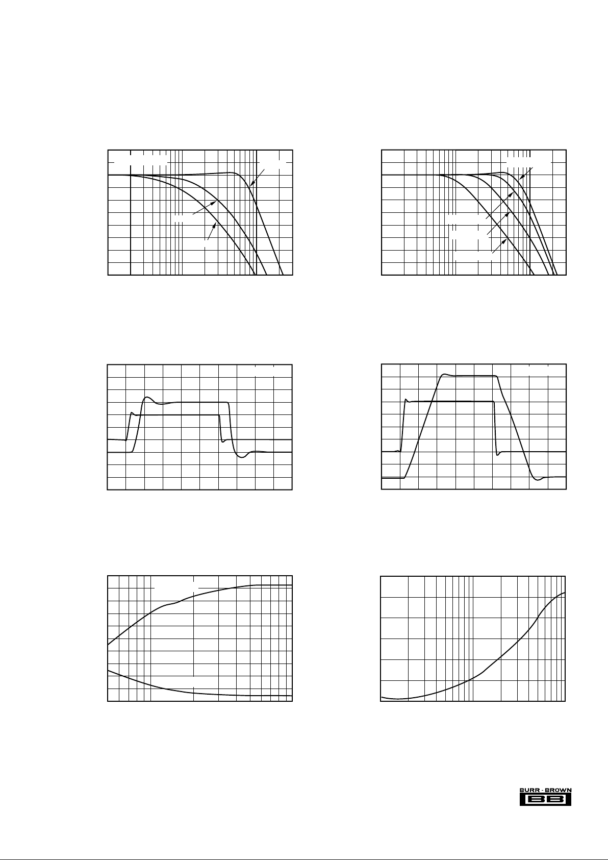
TYPICAL PERFORMANCE CURVES: VS = +5V
At TA = 25°C, G = +2, RF = 750Ω, and RL = 150Ω to VS/ 2, unless otherwise noted (see Figure 2).
6
3
0
–3
–6
–9
–12
–15
–18
–21
–24
SMALL-SIGNAL FREQUENCY RESPONSE
Frequency (MHz)
Normalized Gain (dB)
1 10 100 300
VO = 200mVp-p
G = +10
G = +5
G = +2
12
9
6
3
0
–3
–6
–9
–12
–15
–18
LARGE-SIGNAL FREQUENCY RESPONSE
Frequency (MHz)
Gain (dB)
1 10 100 300
VO = 0.2Vp-p
VO = 4Vp-p
VO = 2Vp-p
VO = 1Vp-p
SMALL-SIGNAL PULSE RESPONSE
Time (10ns/div)
Input and Output Voltage (50mV/div)
VO = 200mVp-p
V
O
V
IN
5.0
4.9
4.8
4.7
4.6
4.5
4.4
4.3
4.2
4.1
4.0
OUTPUT SWING vs LOAD RESISTANCE
R
L
(Ω)
50 100 1000
Maximum Output Voltage (V)
1.0
0.9
0.8
0.7
0.6
0.5
0.4
0.3
0.2
0.1
0.0
Minimum Output Voltage (V)
Maximum V
O
Minimum V
O
LARGE-SIGNAL PULSE RESPONSE
Time (10ns/div)
Input and Output Voltage (500mV/div)
VO = 4Vp-p
V
O
V
IN
–40
–50
–60
–70
–80
–90
–100
CHANNEL-TO-CHANNEL CROSSTALK
Frequency (MHz)
1 10 100
Input-Refered Isolation (dB)
6
®
OPA2631
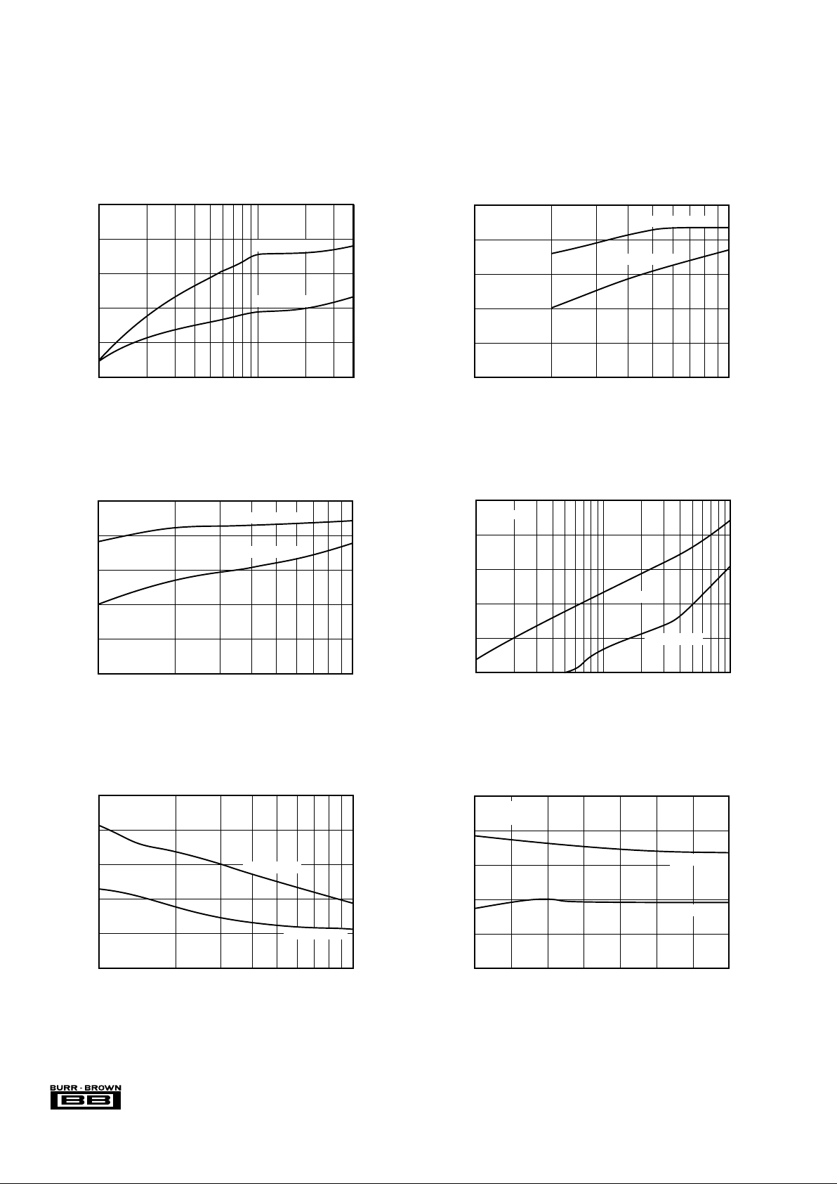
TYPICAL PERFORMANCE CURVES: VS = +5V (Cont.)
At TA = 25°C, G = +2, RF = 750Ω, and RL = 150Ω to VS/ 2, unless otherwise noted (see Figure 1).
–30
–40
–50
–60
–70
–80
HARMONIC DISTORTION vs OUTPUT VOLTAGE
Output Voltage (Vp-p)
0.1 1
f = 5MHz
4
Harmonic Distortion (dBc)
3rd Harmonic
2nd Harmonic
–30
–40
–50
–60
–70
–80
HARMONIC DISTORTION vs INVERTING GAIN
Gain Magnitude (V/V)
110
Harmonic Distortion (dBc)
VO = 2Vp-p
f = 5MHz
3rd Harmonic
2nd Harmonic
–30
–40
–50
–60
–70
–80
HARMONIC DISTORTION vs FREQUENCY
Frequency (MHz)
10.1 10
Harmonic Distortion (dBc)
VO = 2Vp-p
3rd Harmonic
2nd Harmonic
–30
–40
–50
–60
–70
–80
HARMONIC DISTORTION vs LOAD RESISTANCE
R
L
(Ω)
100 1000
Harmonic Distortion (dBc)
VO = 2Vp-p
f
O
= 5MHz
3rd Harmonic
2nd Harmonic
–30
–40
–50
–60
–70
–80
HARMONIC DISTORTION vs SUPPLY VOLTAGE
Single Supply Voltage (V)
389765410
Harmonic Distortion (dBc)
VO = 2Vp-p
f
O
= 5MHz
3rd Harmonic
2nd Harmonic
–30
–40
–50
–60
–70
–80
HARMONIC DISTORTION vs NON-INVERTING GAIN
Gain Magnitude (V/V)
110
Harmonic Distortion (dBc)
VO = 2Vp-p
f = 5MHz
3rd Harmonic
2nd Harmonic
 Loading...