

Burr-Brown OPA2607 User Manual

®
For most current data sheet and other product
information, visit www.burr-brown.com
OPA2607
OPA2607
OPA2607
Dual, High Output, Current-Feedback
TM
OPERATIONAL AMPLIFIER
FEATURES
●
WIDEBAND ±12V OPERATION: 25MHz (G = +8)
● UNITY GAIN STABLE: 35MHz (G = +1)
● HIGH OUTPUT CURRENT: 250mA
● OUTPUT VOLTAGE SWING: ±10.5V (VS = ±12V)
● HIGH SLEW RATE: 600V/µs
● LOW SUPPLY CURRENT: 8mA/channel
● FLEXIBLE POWER CONTROL (SO-14)
● ±6V TO ±16V SUPPLY RANGE
● POWER PACKAGING
APPLICATIONS
● xDSL LINE DRIVER
● LOW-NOISE ADSL RECEIVER
● LOW-COST VIDEO DA
● LOW-COST UPGRADE TO LT1207/AD812
+12V
1/2
OPA2607
1.21kΩ
100nF
4.8Vp-p
348Ω
1.21kΩ
OPA2607
1/2
–12V
Low Turns Ratio ADSL Upstream Driver
78.7Ω
78.7Ω
1:0.8
100Ω
15Vp-p38Vp-p
DESCRIPTION
The OPA2607 provides a high output voltage swing and low
distortion required for low turns ratio ADSL upstream driver
applications. Operating on a ±12V supply, the OPA2607 consumes a low 8.0mA/channel quiescent current to deliver a very
high 250mA peak output current. Guaranteed output current of
180mA supports even the most demanding ADSL CPE requirements with low harmonic distortion. Differential driver applications will deliver < –75dBc distortion at the peak upstream power
levels of full rate ADSL. Using a differential driver design, as
shown below, the OPA2607 can deliver a high 38Vp-p voltage
swing into a 1:0.8 step-down transformer to meet the ADSL CPE
upstream power requirements. This low turns ratio actually provides a step up to the much weaker downstream signal arriving on
the line side of this transformer, extending the DSL modem’s
reach.
Power control features are included in the SO-14 package version
to allow system power to be minimized. Two logic control lines
allow four quiescent power settings. These include full power,
power cutback for short loops, idle state for no signal transmission
but line match maintenance, and shutdown for power off with a
high impedance output. An additional I
mum supply current to be adjusted ±25% from the nominal value.
Connecting this pin to +VCC will increase the full power quiescent
to 20mA, increasing the peak output current available, while
connecting this pin to –V
will decrease the full power quiescent
CC
to 12mA where a lower peak output current is required. The
digital control lines continue to scale the total quiescent current
from these new maximum levels in the same proportional steps as
before.
The OPA2607 is available in three package styles. For power
driver applications, a thermally enhanced
with a heat slug is available in both SO-8 and SO-14 pinouts. For
lower power receiver applications, a standard SO-8 package is
available.
OPA2607 RELATED PRODUCTS
SINGLES DUALS TRIPLES NOTES
OPA681 OPA2681 OPA3681 Single +12V Capable
— OPA2677 — Single +12V Capable
pin allows the maxi-
ADJ
package
SBOS128
International Airport Industrial Park • Mailing Address: PO Box 11400, Tucson, AZ 85734 • Street Address: 6730 S. Tucson Blvd., Tucson, AZ 85706 • Tel: (520) 746-1111
Twx: 910-952-1111 • Internet: http://www.burr-brown.com/ • Cable: BBRCORP • Telex: 066-6491 • FAX: (520) 889-1510 • Immediate Product Info: (800) 548-6132
©
2000 Burr-Brown Corporation PDS-1615A Printed in U.S.A. August, 2000
1
OPA2607
®
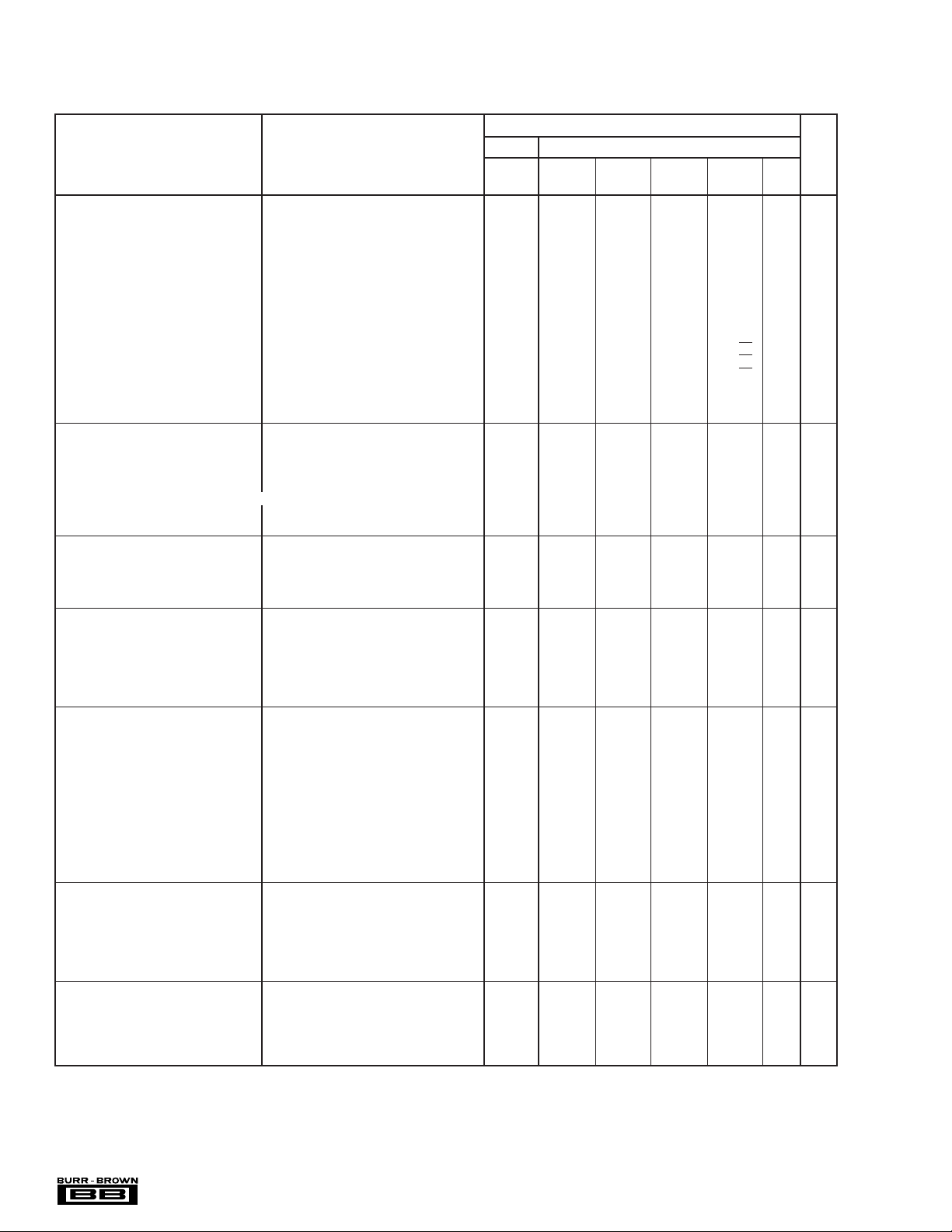
SPECIFICATIONS: VS = ±12V
RF = 1.21kΩ, RL = 100Ω, and G = +8, unless otherwise noted.
OPA2607H, U, N
TYP GUARANTEED
PARAMETER CONDITIONS +25°C +25°C
(2)
70°C
(3)
+85°C
(3)
UNITS MAX
0°C to –40°C to
AC PERFORMANCE (see Figure 1)
Small-Signal Bandwidth (V
Bandwidth for 0.1dB Gain Flatness G = +8, V
Large-Signal Bandwidth G = +8, VO = 20Vp-p 13 10.6 9.0 7.9 MHz min B
Slew Rate G = +8, V
Rise/Fall Time G = +8, V
Spurious Free Dynamic Range
Input Voltage Noise 1.7 2.0 2.6 2.7 nV/√Hz max B
= 0.5Vp-p) G = +1, RF = 1.50kΩ 35 MHz typ C
O
(4)
G = +2, R
G = +4, R
G = +8, R
VO = 2Vp-p, 1MHz, RL = 100Ω 77 66 60 57 dB min B
V
= 20Vp-p, 150kHz, RL = 150Ω 75 70 58 57 dB min B
O
= 1.43kΩ 28 MHz typ C
F
= 1.37kΩ 25 MHz typ C
F
= 1.21kΩ 25 19 18 17 MHz min B
F
= 0.5Vp-p 6 MHz typ C
O
= 20V Step 600 470 400 350 V/µs min B
O
= 0.5V Step 14 18 20 21 ns min B
O
Non-Inverting Input Current Noise 11 13 13 13 pA/√Hz max B
Inverting Input Current Noise 15 17 17 17 pA/√Hz max B
Differential Gain NTSC, G = +2, R
Differential Phase NTSC, G = +2, R
Channel-to-Channel Crosstalk f = 1MHz –60 dB typ C
DC PERFORMANCE
Open-Loop Transimpedance Gain
(5)
VO = 0V, RL = 100Ω 950 440 390 310 kΩ min A
Input Offset Voltage V
Average Offset Voltage Drift V
Non-Inverting Input Bias Current V
Average Non-Inverting Input Bias Current Drift V
Inverting Input Bias Current V
Average Inverting Input Bias Current Drift
= 150Ω 0.01 % typ C
L
= 150Ω 0.01 degrees typ C
L
= 0V ±1.5 ±7 ±8 ±8.5 mV max A
CM
= 0V –20 –25 µV/°C max B
CM
= 0V ±3 ±12 ±15 ±20 µA max A
CM
= 0V –70 –100 nA/°C max B
CM
= 0V ±4 ±40 ±58 ±70 µA max A
CM
VCM = 0V –380 –425 nA/°C max B
INPUT
Common-Mode Input Range
(CMIR)
Common-Mode Rejection Ratio
(CMRR)
VCM = 0V 64 53 52 51 dB min A
±10.3 ±10.0 ±9.9 ±9.8 V min A
Non-Inverting Input Impedance 250 || 4 kΩ || pF typ C
Inverting Input Resistance
Open-Loop 33 Ω typ C
OUTPUT
Voltage Output Swing No Load, Hard Limit ±11.2 ±10.9 ±10.8 ±10.7 V min A
R
= 100Ω, Hard Limit ±10.5 ±9.9 ±9.8 ±9.7 V min A
L
R
= 150Ω, SFDR > 67dB, 150kHz ±10.2 V typ C
Current Output, Sourcing V
Current Output, Sinking V
Closed-Loop Output Impedance G = +8, f ≤ 10kHz 0.02 Ω typ C
Power Control
(SO-14 only) DIG_REF = Gnd
L
= 0 310 210 175 140 mA min A
O
= 0 250 180 150 110 mA min A
O
Maximum Logic 0 A0, A1 0.8 V max C
Minimum Logic 1 A0, A1 2 V min C
Logic Input Current 0V to 4.5V 60 µA max C
Supply Current at Full Power A0 = 1, A1 = 1, I
Supply Current at Power Cutback A0 = 0, A1 = 1, I
Supply Current at Idle Power A0 = 1, A1 = 0, I
Supply Current at Shutdown A0 = 0, A1 = 0, I
Output Impedance in Idle Power Closed-Loop, f < 1MHz 0.7 Ω typ C
= open 16 mA typ C
ADJ
= open 13 mA typ C
ADJ
= open 3.8 mA typ C
ADJ
= open 1.3 mA typ C
ADJ
Output Impedance in Shutdown 350 || 17 kΩ || pF typ C
Shutdown Isolation G = +8, 1MHz 75 dB typ C
Maximum Adjusted Quiescent Current A0 = 1, A1 = 1, I
Minimum Adjusted Quiescent Current A0 = 1, A1 = 1, I
ADJ
ADJ
at +V
at –V
S
S
20 mA typ C
12 mA typ C
POWER SUPPLY
Minimum Operating Voltage ±6 ±6 ±6 V min B
Specified Operating Voltage ±12 V typ C
Maximum Operating Voltage ±16 ±16 ±16 V max A
Maximum Quiescent Current Total Both Channels, Full Power 16 16.8 17 17.5 mA max A
Minimum Quiescent Current Total Both Channels, Full Power 16 15.2 13.8 13.3 mA min A
Power Supply Rejection Ratio (PSRR) f ≤ 10kHz 68 61 59 57 dB min A
TEMPERATURE RANGE
Specification: H, U, N
Thermal Resistance,
H PSO-8 Power Package
U SO-8 125 °C/W typ C
N PSO-14 Power Package
θ
JA
(6)
(6)
Junction-to-Ambient
–40 to +85
50 °C/W typ C
45 °C/W typ C
NOTES: (1) Test Levels: (A) 100% tested at 25°C. Over temperature limits by characterization and simulation. (B) Limits set by characterization and simulation.
(C) Typical value only for information. (2) Junction temperature = ambient for 25°C guaranteed specifications. (3) Junction temperature = ambient at low temperature
limit: junction temperature = ambient +40°C at high temperature limit for over temperature guaranteed specifications. (4) Single amplifier SFDR limited by 2nd Harmonic.
Differential SFDR will be limited by 3rd Harmonic and will be > 15dB higher. (5) Current is considered positive out of node. V
(6) Slug in power package connected to –V
plane at least 2" x 2" (50mm x 50mm) in size. See the Board Layout Guidelines Section.
S
is the input common-mode voltage.
CM
MIN/
TEST
LEVEL
°C typ C
(1)
®
OPA2607
2
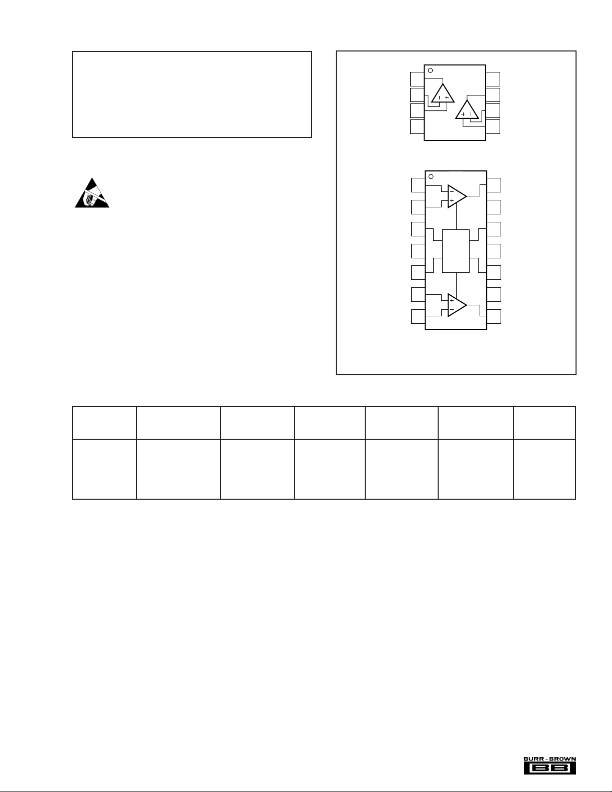
ABSOLUTE MAXIMUM RATINGS
1
2
3
4
5
6
7
14
13
12
11
10
9
8
–In A
+In A
A0
–V
S
A1
+In B
–In B
Out A
NC
DIG_REF
+V
S
I
ADJ
NC
Out B
NC = No Connection
PSO-14
Power
Control
Power Supply ............................................................................. ±16.5V
Internal Power Dissipation
Differential Input Voltage ..................................................................... ±5V
Input Voltage Range ............................................................................ ±V
Storage Temperature Range: U, N................................ –40°C to +125°C
Lead Temperature (soldering, 10s) .............................................. +260°C
Junction Temperature (T
ESD Rating (Human Body Model) .................................................. 4000V
(Machine Model) ........................................................... 300V
NOTE:: (1) Packages must be derated based on specified
must be observed.
(1)
............................ See Thermal Information
) ........................................................... +175°C
J
θ
. Maximum T
JA
DC
S
ELECTROSTATIC
DISCHARGE SENSITIVITY
Electrostatic discharge can cause damage ranging from performance degradation to complete device failure. Burr-Brown
Corporation recommends that all integrated circuits be handled
and stored using appropriate ESD protection methods.
ESD damage can range from subtle performance degradation to
complete device failure. Precision integrated circuits may be
more susceptible to damage because very small parametric
changes could cause the device not to meet published specifications.
PIN CONFIGURATIONS
Top View
J
Out A
–In A
+In A
–V
1
2
3
4
S
SO-8, PSO-8
+V
8
S
Out B
7
–In B
6
+In B
5
PACKAGE/ORDERING INFORMATION
PACKAGE SPECIFIED
PRODUCT PACKAGE NUMBER RANGE MARKING NUMBER
OPA2607H PSO-8 182-1 –40°C to +85°C OPA2607H OPA2607H Rails
" " " " " OPA2607H/2K5 Tape and Reel
OPA2607U SO-8 182 " OPA2607U OPA2607U Rails
" " " " " OPA2607U/2K5 Tape and Reel
OPA2607N PSO-14 235-1 " OPA2607N Contact Factory Rails
" " " " " Contact Factory Tape and Reel
NOTE: (1) Models with a slash (/) are available only as Tape and Reel in the quantity indicated after the slash (e.g. /2K5 indicates 2500 devices per reel). Ordering 2500
pieces of the OPA2607U/2K5 will get a single 2500-piece Tape and Reel.
DRAWING TEMPERATURE PACKAGE ORDERING TRANSPORT
(1)
MEDIA
The information provided herein is believed to be reliable; however, BURR-BROWN assumes no responsibility for inaccuracies or omissions. BURR-BROWN assumes
no responsibility for the use of this information, and all use of such information shall be entirely at the user’s own risk. Prices and specifications are subject to change
without notice. No patent rights or licenses to any of the circuits described herein are implied or granted to any third party. BURR-BROWN does not authorize or warrant
any BURR-BROWN product for use in life support devices and/or systems.
®
3
OPA2607
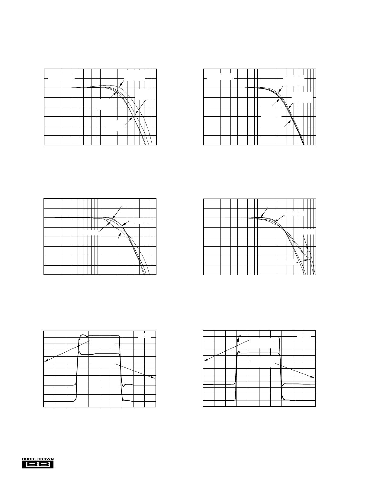
TYPICAL PERFORMANCE CURVES: VS = ±12V
At TA = +25°C, G = +8, RF = 1.21kΩ, and RL = 100Ω, unless otherwise noted. See Figure 1 for AC performance only.
NON-INVERTING SMALL-SIGNAL
FREQUENCY RESPONSE
6
3
VO = 0.5Vp-p
G = +1
= 1.50kΩ
R
F
0
–3
–6
G = +4
R
= 1.37kΩ
F
–9
Normalized Gain (dB)
–12
G = +8
R
= 1.21kΩ
F
–15
–18
1M 10M 100M
Frequency (Hz)
NON-INVERTING LARGE-SIGNAL
FREQUENCY RESPONSE
6
3
0
G = +8
VO = 0.5Vp-p
VO = 2Vp-p
–3
–6
–9
Normalized Gain (dB)
–12
VO = 8Vp-p
VO = 16Vp-p
–15
–18
1M 10M 100M
Frequency (Hz)
G = +2
= 1.43kΩ
R
F
INVERTING SMALL-SIGNAL
FREQUENCY RESPONSE
6
VO = 0.5Vp-p
3
0
–3
–6
–9
Normalized Gain (dB)
–12
–15
G = –2
= 1.40kΩ
R
F
R
F
G = –4
= 1.30kΩ
G = –8
= 1.18kΩ
R
F
R
–18
1M 10M 100M
Frequency (Hz)
INVERTING LARGE-SIGNAL
FREQUENCY RESPONSE
6
G = –8
3
0
–3
VO = 0.5Vp-p
VO = 2Vp-p
VO = 16Vp-p
–6
–9
Normalized Gain (dB)
–12
–15
VO = 8Vp-p
–18
1M 10M 100M
Frequency (Hz)
G = –1
= 1.43kΩ
F
NON-INVERTING PULSE RESPONSE
Output Voltage (2V/div)
®
OPA2607
VO = 20Vp-p
Large Signal
VO = 0.5Vp-p
Small Signal
Time (100ns/div)
G = +8
Output Voltage (100mV/div)
Output Voltage (2V/div)
4
INVERTING PULSE RESPONSE
G = –8
VO = 20Vp-p
Large Signal
VO = 0.5Vp-p
Small Signal
Output Voltage (100mV/div)
Time (100ns/div)
 Loading...