

Burr Brown OPA2541BM, OPA2541AM-BI, OPA2541AM, OPA2541SM Datasheet
DESCRIPTION
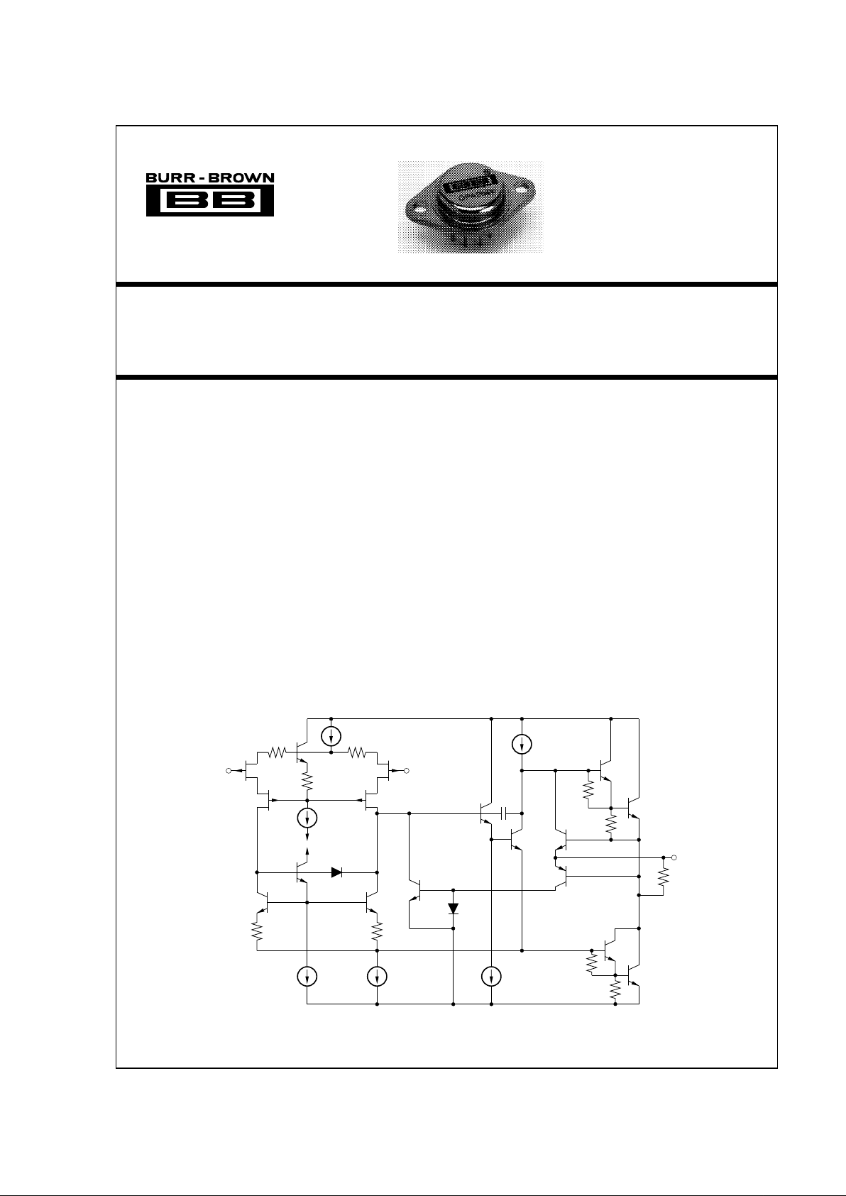
The OPA2541 is a dual power operational amplifier
capable of operation from power supplies up to ±40V
and output currents of 5A continuous. With two monolithic power amplifiers in a single package it provides
unequaled functional density.
The industry-standard 8-pin TO-3 package is isolated
from all internal circuitry allowing it to be mounted
directly to a heat sink without insulators which degrade thermal performance. Internal circuitry limits
output current to approximately 6A.
The OPA2541 is available in both industrial and
military temperature range versions.
Dual High Power
OPERATIONAL AMPLIFIER
FEATURES
● OUTPUT CURRENTS TO 5A
● POWER SUPPLIES TO
±40V
● FET INPUT
● ELECTRICALLY ISOLATED CASE
APPLICATIONS
● MOTOR DRIVER
● SERVO AMPLIFIER
● SYNCRO/RESOLVER EXCITATION
● VOICE COIL DRIVER
● BRIDGE AMPLIFIER
● PROGRAMMABLE POWER SUPPLY
● AUDIO AMPLIFIER
OPA2541
Out
(5, 1)
–VS (6)
+V
S
(2)
+In
(3, 7)
–In
(4, 8)
®
International Airport Industrial Park • Mailing Address: PO Box 11400 • Tucson, AZ 85734 • Street Address: 6730 S. Tucson Blvd. • Tucson, AZ 85706
Tel: (520) 746-1111 • Twx: 910-952-1111 • Cable: BBRCORP • Telex: 066-6491 • FAX: (520) 889-1510 • Immediate Product Info: (800) 548-6132
©
1987 Burr-Brown Corporation PDS-768B Printed in U.S.A. October, 1993
®
OPA2541
2
The information provided herein is believed to be reliable; however, BURR-BROWN assumes no responsibility for inaccuracies or omissions. BURR-BROWN assumes
no responsibility for the use of this information, and all use of such information shall be entirely at the user’s own risk. Prices and specifications are subject to change
without notice. No patent rights or licenses to any of the circuits described herein are implied or granted to any third party. BURR-BROWN does not authorize or warrant
any BURR-BROWN product for use in life support devices and/or systems.
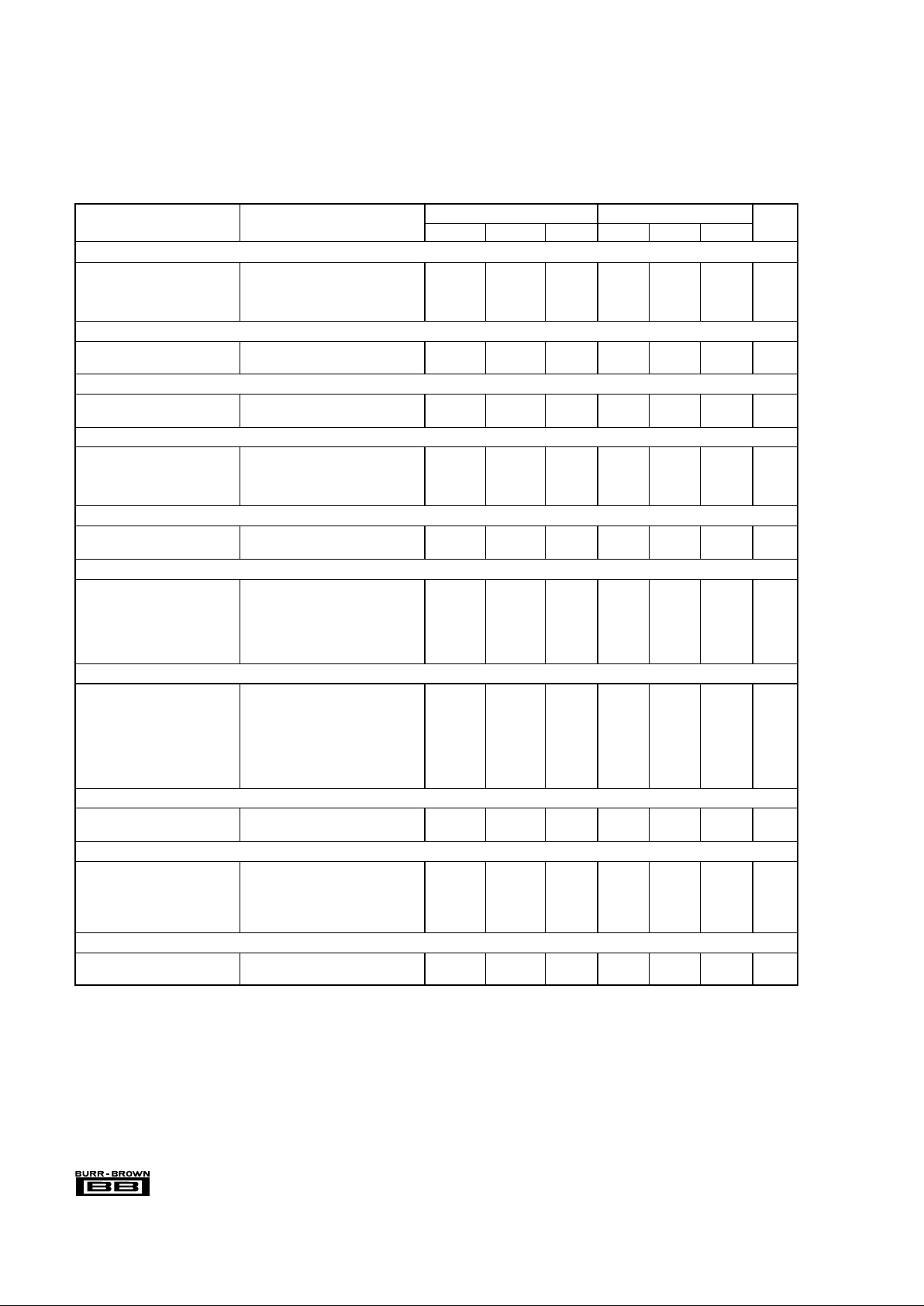
SPECIFICATIONS
ELECTRICAL
At TC = +25°C and VS = ±35VDC, unless otherwise noted.
OPA2541AM OPA2541BM, SM
PARAMETER CONDITIONS MIN TYP MAX MIN TYP MAX UNITS
INPUT OFFSET VOLTAGE
V
OS
±2 ±10 ±0.25 ±1mV
vs Temperature Specified Temperature Range ±20 ±40 ±15 ±30 µV/°C
vs Supply Voltage V
S
= ±10V to ±V
MAX
±2.5 ±10 * * µV/V
vs Power ±20 ±60 * * µV/W
INPUT BIAS CURRENT
I
B
15 50 * * pA
Specified Temperature Range Note 1 *
INPUT OFFSET CURRENT
I
OS
±5 ±30 * * pA
Specified Temperature Range Note 1 *
INPUT CHARACTERISTICS
Common-Mode Voltage Range Specified Temperature Range ±(|V
S
| –6) ±(|VS| –3) * * V
Common-Mode Rejection V
CM
= (|±VS| –6V) 95 106 * * dB
Input Capacitance 5*pF
Input Impedance, DC 1*10
12
Ω
GAIN CHARACTERISTICS
Open Loop Gain at 10Hz R
L
= 6Ω 90 96 * * dB
Gain-Bandwidth Product 1.6 * MHz
OUTPUT
Voltage Swing I
O
= 5A ±(|VS| –5.5) ±(|VS| –4.5) * * V
I
O
= 2A ±(|VS| –4.5) ±(|VS| –3.6) * * V
I
O
= 0.5A ±(|VS| –4) ±(|VS| –3.2) * * V
Current, Continuous +25°C 5 7.0 * * A
+85°C 4 5.0 * A
+125°C (SM grade only) 3 3.5 A
AC PERFORMANCE
Slew Rate 68 ** V/µs
Power Bandwidth R
L
= 8Ω, VO = 20Vrms 45 55 * * kHz
Settling Time to 0.1% 2V Step 2 * µs
Capacitive Load Specified Temperature Range, G = 1 3.3 * nF
Specified Temperature Range, G >10 SOA *
Phase Margin Specified Temperature Range, R
L
= 8Ω 40 * Degrees
Channel Separation 1kHz, R
L
= 6Ω 80 * dB
POWER SUPPLY
Power Supply Voltage, ±V
S
Specified Temperature Range ±10 ±30 ±35 * ±35 ±40 V
Current, Quiescent Total—Both Amplifiers 40 50 * * mA
THERMAL RESISTANCE
θ
JC
, (Junction-to-Case) Both Amplifiers
(2)
, AC Output f > 60Hz 0.8 1.0 * * °C/W
θ
JC
Both Amplifiers
(2)
, DC Output 0.9 1.2 * * °C/W
θ
JC
One Amplifier, AC Output f > 60Hz 1.25 1.5 * * °C/W
θ
JC
One Amplifier, DC Output 1.4 1.9 * * °C/W
θ
JA
, (Junction-to-Ambient) No Heat Sink 30 * °C/W
TEMPERATURE RANGE
Case AM, BM –25 +85 * * °C
SM –55 +125 °C
*Specification same as OPA2541AM.
NOTES: (1) Input bias and offset current approximately doubles for every 10°C increase in temperature. (2) Assumes equal dissipation in both amplifiers.
®
OPA2541
3
100
10
1
0.1
0.01
0.001
–25 25 100 125
Junction Temperature (°C)
INPUT BIAS CURRENT vs TEMPERATURE
Input Bias Current (nA)
05075
TYPICAL PERFORMANCE CURVES
TA = +25°C and VS = ±35VDC, unless otherwise noted.
Supply Voltage, +VS to –VS..................................................................80V
Output Current .............................................................................see SOA
Power Dissipation, Internal
(1)
............................................................125W
Input Voltage: Differential..................................................................... ±V
S
Common-mode ............................................................. ±V
S
Temperature: Pin Solder, 10s ........................................................+300°C
Junction
(1)
............................................................... +150°C
Temperature Range:
Storage .................................................... –65°C to +150°C
Operating (Case) ..................................... –55°C to +125°C
NOTE: (1) Long term operation at the maximum junction temperature will
result in reduced product life. Derate internal power dissipation to achieve
high MTTF.
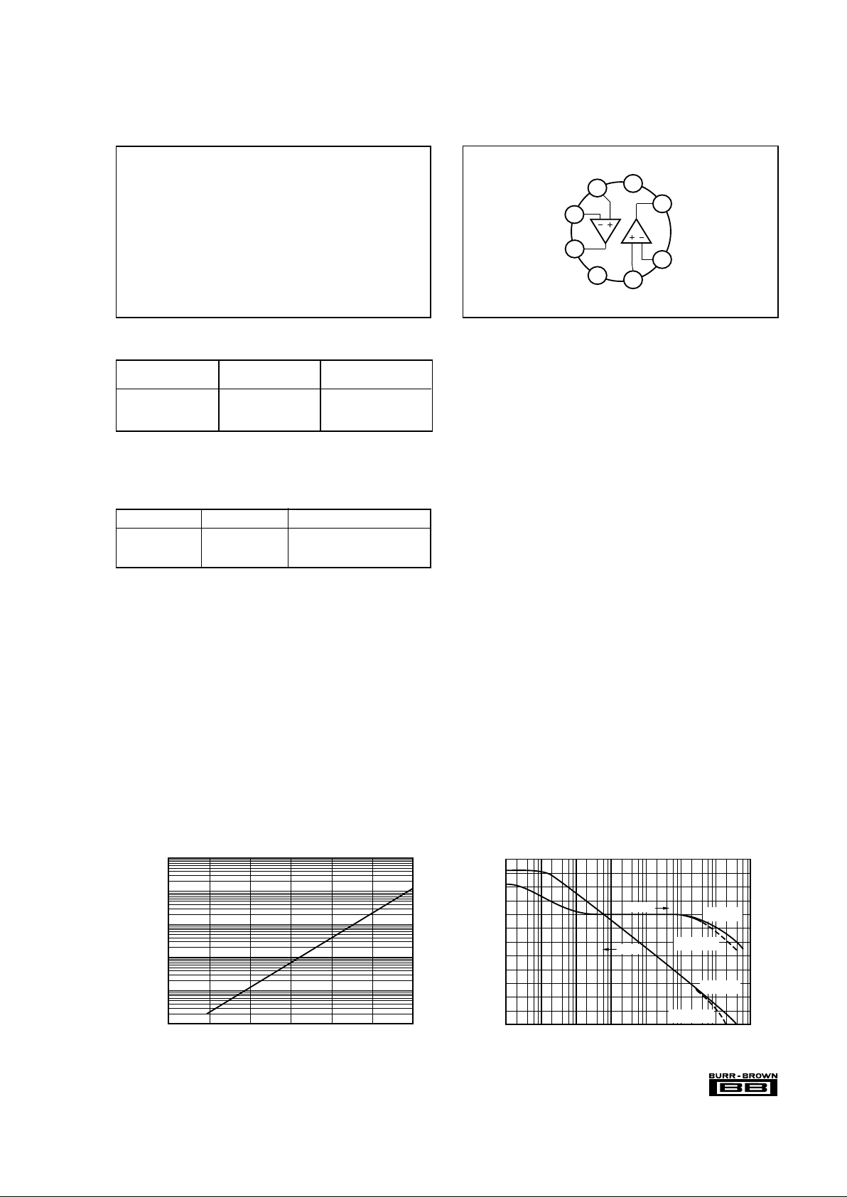
ABSOLUTE MAXIMUM RATINGS CONNECTION DIAGRAM
1
2
3
7
8
5
6
A
B
+V
S
+In
B
–In
B
Out
B
–V
S
Out
A
–In
A
+In
A
4
ORDERING INFORMATION
PACKAGE INFORMATION
PACKAGE DRAWING
MODEL PACKAGE NUMBER
(1)
OPA2541AM TO-3 030
OPA2541BM TO-3 030
OPA2541SM TO-3 030
NOTE: (1) For detailed drawing and dimension table, please see end of data
sheet, or Appendix D of Burr-Brown IC Data Book.
Top View TO-3
MODEL PACKAGE TEMPERATURE RANGE
OPA2541AM TO-3 –25°C to +85°C
OPA2541BM TO-3 –25°C to +85°C
OPA2541SM TO-3 –55°C to +125°C
1 100 100k 10M
Frequency (Hz)
OPEN-LOOP GAIN AND PHASE vs FREQUENCY
10 1k 10k 1M
110
100
90
80
70
60
50
40
30
20
10
0
Voltage Gain (dB)
–10
0
–45
–90
–135
–180
Phase (Degrees)
ZL = 3.3nF
Phase
Gain
ZL = 2kΩ
ZL = 3.3nF
ZL = 2kΩ
 Loading...