

BURR-BROWN OPA241 User Manual
®
OPA241
OPA4251
OPA241
OPA2241
OPA4241
OPA4241
Single-Supply,
OPERATIONAL AMPLIFIERS
OPA241 Family optimized for +5V supply.
OPA251 Family optimized for ±15V supply.
FEA TURES
●
Micro
POWER: IQ = 25µA
● SINGLE-SUPPLY OPERATION
● RAIL-TO-RAIL OUTPUT (within 50mV)
● WIDE SUPPLY RANGE
Single Supply: +2.7V to +36V
Dual Supply: ±1.35V to ±18V
● LOW OFFSET VOLTAGE: ±250µV max
● HIGH COMMON-MODE REJECTION: 124dB
● HIGH OPEN-LOOP GAIN: 128dB
● SINGLE, DUAL, AND QUAD
APPLICATIONS
● BATTERY OPERATED INSTRUMENTS
● PORTABLE DEVICES
● MEDICAL INSTRUMENTS
● TEST EQUIPMENT
OPA2251
OPA251
OPA2251
OPA4251
Micro
POWER
DESCRIPTION
The OPA241 series and OPA251 series are specifically
designed for battery powered, portable applications. In addition to very low power consumption (25µA), these amplifiers feature low offset voltage, rail-to-rail output swing, high
common-mode rejection, and high open-loop gain.
The OPA241 series is optimized for operation at low power
supply voltage while the OPA251 series is optimized for
high power supplies. Both can operate from either single
(+2.7V to +36V) or dual supplies (±1.35V to ±18V). The
input common-mode voltage range extends 200mV below
the negative supply—ideal for single-supply applications.
They are unity-gain stable and can drive large capacitive
loads. Special design considerations assure that these products are easy to use. High performance is maintained as the
amplifiers swing to their specified limits. Because the initial
offset voltage (±250µV max) is so low, user adjustment is
usually not required. However, external trim pins are provided for special applications (single versions only).
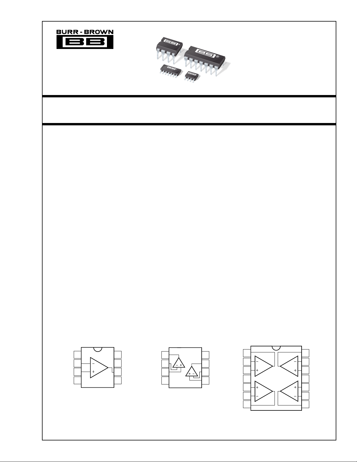
The OPA241 and OPA251 (single versions) are available
in standard 8-pin DIP and SO-8 surface-mount packages.
The OPA2241 and OPA2251 (dual versions) come in 8-pin
DIP and SO-8 surface-mount packages. The OPA4241 and
OPA4251 (quad versions) are available in 14-pin DIP and
SO-14 surface-mount packages. All are fully specified
from –40°C to +85°C and operate from –55°C to +125°C.
SBOS075
OPA241, OPA251
Offset Trim
International Airport Industrial Park • Mailing Address: PO Box 11400, Tucson, AZ 85734 • Street Address: 6730 S. Tucson Blvd., Tucson, AZ 85706 • Tel: (520) 746-1111 • Twx: 910-952-1111
Internet: http://www.burr-brown.com/ • FAXLine: (800) 548-6133 (US/Canada Only) • Cable: BBRCORP • Telex: 066-6491 • FAX: (520) 889-1510 • Immediate Product Info: (800) 548-6132
© 1997 Burr-Brown Corporation PDS-1406B Printed in U.S.A. October, 1998
–In
+In
1
2
3
V–
4
8-Pin DIP, SO-8
8
7
6
5
NC
V+
Output
Offset Trim
Out A
–In A
+In A
OPA2241, OPA2251
1
2
3
V–
4
A
B
8-Pin DIP, SO-8
1
V+
8
Out B
7
–In B
6
+In B
5
Out A
–In A
+In A
V+
+In B
–In B
Out B
OPA4241, OPA4251
1
2
AD
3
4
5
BC
6
7
14-Pin DIP, SO-14
OPA241, 2241, 4241
OPA251, 2251, 4251
Out D
14
–In D
13
+In D
12
V–
11
+In C
10
–In C
9
Out C
8
®
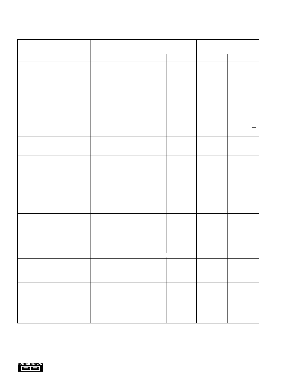
SPECIFICATIONS: VS = 2.7V to 5V
At TA = +25°C, RL = 100kΩ connected to VS/2, unless otherwise noted.
Boldface limits apply over the specified temperature range, T
PARAMETER CONDITION MIN TYP
OFFSET VOLTAGE
Input Offset Voltage V
T
= –40°C to +85°C ±100 ±400 ±130 µV
A
vs Temperature dV
vs Power Supply PSRR V
T
= –40°C to +85°C VS = 2.7V to 36V 30 ✻ µV/V
A
Channel Separation (dual, quad) 0.3 ✻ µV/V
INPUT BIAS CURRENT
Input Bias Current
T
= –40°C to +85°C –25 nA
A
Input Offset Current I
T
= –40°C to +85°C ±2 nA
A
(2)
OS
/dT TA = –40°C to +85°C ±0.4 ±0.6 µV/°C
OS
I
B
OS
NOISE
Input Voltage Noise, f = 0.1Hz to 10Hz 1 ✻ µVp-p
Input Voltage Noise Density, f = 1kHz e
Current Noise Density, f = 1kHz i
n
n
INPUT VOLTAGE RANGE
Common-Mode Voltage Range V
Common-Mode Rejection Ratio CMRR V
T
= –40°C to +85°C V
A
CM
INPUT IMPEDANCE
Differential 10
Common-Mode 10
OPEN-LOOP GAIN
Open-Loop Voltage Gain A
T
= –40°C to +85°C
A
T
= –40°C to +85°C
A
= 100kΩ, VO = (V–)+100mV to (V+)–100mV
OLRL
RL = 100kΩ, VO = (V–)+100mV to (V+)–100mV
RL = 10kΩ, VO = (V–)+200mV to (V+)–200mV
RL = 10kΩ, VO = (V–)+200mV to (V+)–200mV
FREQUENCY RESPONSE
Gain-Bandwidth Product GBW 35 ✻ kHz
Slew Rate SR V
Overload Recovery Time V
OUTPUT
Voltage Output Swing from Rail
T
= –40°C to +85°C RL = 100kΩ to VS/2, A
A
T
= –40°C to +85°C RL = 10kΩ to VS/2, A
A
Short-Circuit Current I
Single Versions –24/+4 ✻ mA
(3)
V
RL = 100kΩ to VS/2, A
O
R
L
R
SC
Dual, Quad Versions –30/+4 ✻ mA
Capacitive Load Drive C
LOAD
POWER SUPPLY
Specified Voltage Range V
Operating Voltage Range T
Quiescent Current (per amplifier) I
T
= –40°C to +85°C IO = 0 ±36 µA
A
S
Q
TEMPERATURE RANGE
Specified Range –40 +85 ✻✻°C
Operating Range –55 +125 ✻✻°C
Storage Range –55 +125 ✻✻°C
Thermal Resistance
8-Pin DIP 100 ✻ °C/W
θ
JA
SO-8 Surface Mount 150 ✻ °C/W
14-Pin DIP 80 ✻ °C/W
SO-14 Surface Mount 100 ✻ °C/W
✻ Specifications the same as OPA241UA, PA.
NOTES: (1) V
output and power supply rails.
= +5V. (2) The negative sign indicates input bias current flows out of the input terminals. (3) Output voltage swings are measured between the
S
The information provided herein is believed to be reliable; however, BURR-BROWN assumes no responsibility for inaccuracies or omissions. BURR-BROWN assumes
no responsibility for the use of this information, and all use of such information shall be entirely at the user’s own risk. Prices and specifications are subject to change
without notice. No patent rights or licenses to any of the circuits described herein are implied or granted to any third party. BURR-BROWN does not authorize or warrant
any BURR-BROWN product for use in life support devices and/or systems.
= –40°C to +85°C.
A
OPA241UA, PA OPA251UA, PA
OPA2241UA, PA OPA2251UA, PA
OPA4241UA, PA OPA4251UA, PA
(1)
MAX MIN TYP
(1)
±50 ±250 ±100 µV
= 2.7V to 36V 3 30 ✻✻µV/V
S
–4 –20 ✻ nA
±0.1 ±2 ✻ nA
45 ✻ nV/√Hz
40 ✻ fA/√Hz
= –0.2V to (V+) –0.8V 80 106 ✻ dB
–0.2
CM
= 0V to (V+) –0.8V 80 dB
CM
(V+) –0.8
7
|| 2 ✻ Ω || pF
9
|| 4 ✻ Ω || pF
100 120 ✻ dB
100 dB
100 120 ✻ dB
100 dB
= 5V, G = 1 0.01 ✻ V/µs
S
• G = V
IN
= 100kΩ to VS/2, A
= 10kΩ to VS/2, A
L
S
≥ 70dB 50 ✻ mV
OL
≥ 100dB 75 100 ✻ mV
OL
≥ 100dB 100 mV
OL
≥ 100dB 100 200 ✻ mV
OL
≥ 100dB 200 mV
OL
60 ✻ µs
See Typical Curve ✻
= –40°C to +85°C +2.7 +36 ✻✻V
+2.7 to +5
A
IO = 0 ±25 ±30 ✻ µA
✻ V
MAX UNITS
V
®
OPA241, 2241, 4241
OPA251, 2251, 4251
2
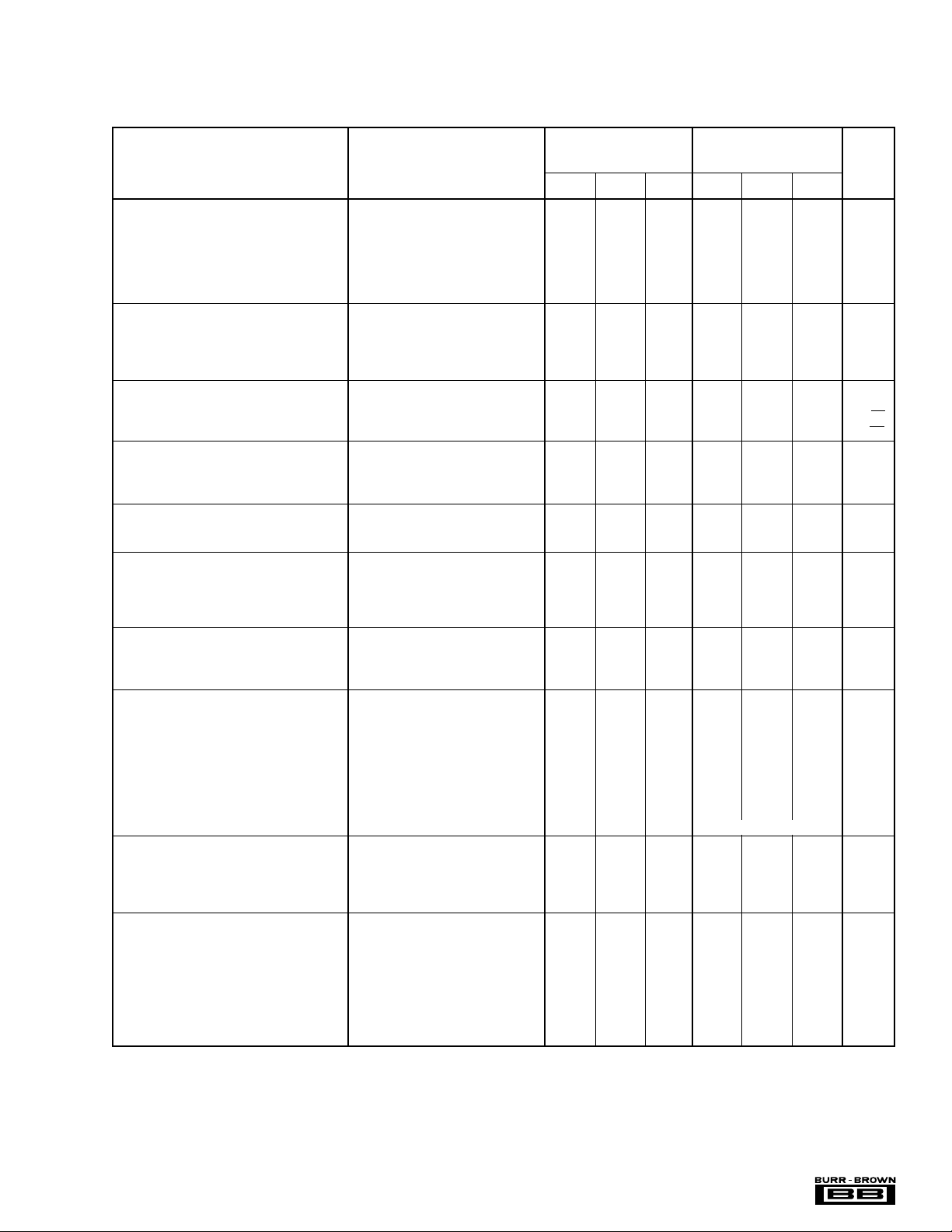
SPECIFICATIONS: VS = ±15V
At TA = +25°C, RL = 100kΩ connected to ground, unless otherwise noted.
Boldface limits apply over the specified temperature range, T
PARAMETER CONDITION MIN TYP MAX MIN TYP MAX UNITS
OFFSET VOLTAGE
Input Offset Voltage V
T
= –40°C to +85°C ±150 ±100 ±300 µV
A
vs Temperature dV
vs Power Supply PSRR V
T
= –40°C to +85°C VS = ±1.35V to ±18V ✻ 30 µV/V
A
Channel Separation (dual, quad) ✻ 0.3 µV/V
INPUT BIAS CURRENT
Input Bias Current
T
= –40°C to +85°C –25 nA
A
Input Offset Current I
T
= –40°C to +85°C ±2 nA
A
(1)
OS
/dT TA = –40°C to +85°C ±0.6 ±0.5 µV/°C
OS
I
B
OS
NOISE
Input Voltage Noise, f = 0.1Hz to 10Hz ✻ 1 µVp-p
Input Voltage Noise Density, f = 1kHz e
Current Noise Density, f = 1kHz i
n
n
INPUT VOLTAGE RANGE
Common-Mode Voltage Range V
Common-Mode Rejection Ratio CMRR V
T
= –40°C to +85°C V
A
CM
INPUT IMPEDANCE
Differential ✻ 10
Common-Mode ✻ 10
OPEN-LOOP GAIN
Open-Loop Voltage Gain A
T
= –40°C to +85°C
A
T
= –40°C to +85°C
A
= 100kΩ, VO = –14.75V to +14.75V
OLRL
RL = 100kΩ, VO = –14.75V to +14.75V
RL = 20kΩ, VO = –14.7V to +14.7V
RL = 20kΩ, VO = –14.7V to +14.7V
FREQUENCY RESPONSE
Gain-Bandwidth Product GBW ✻ 35 kHz
Slew Rate SR G = 1 ✻ 0.01 V/µs
Overload Recovery Time V
OUTPUT
Voltage Output Swing from Rail
T
= –40°C to +85°C RL = 100kΩ, A
A
T
= –40°C to +85°C RL = 20kΩ, A
A
Short-Circuit Current I
Single Versions ✻ –21/+4 mA
(2)
V
O
SC
Dual Versions ✻ –50/+4 mA
Capacitive Load Drive C
LOAD
POWER SUPPLY
Specified Voltage Range V
Operating Voltage Range T
Quiescent Current (per amplifier) I
T
= –40°C to +85°C IO = 0 ±45 µA
A
S
Q
TEMPERATURE RANGE
Specified Range ✻✻–40 +85 °C
Operating Range ✻✻–55 +125 °C
Storage Range ✻✻–55 +125 °C
Thermal Resistance
8-Pin DIP ✻ 100 °C/W
θ
JA
SO-8 Surface Mount ✻ 150 °C/W
14-Pin DIP ✻ 80 °C/W
SO-14 Surface Mount ✻ 100 °C/W
✻ Specifications the same as OPA251UA, PA.
NOTES: (1) The negative sign indicates input bias current flows out of the input terminals. (2) Output voltage swings are measured between the output and
power supply rails.
= –40°C to +85°C.
A
OPA241UA, PA OPA251UA, PA
OPA2241UA, PA OPA2251UA, PA
OPA4241UA, PA OPA4251UA, PA
±100 ±50 ±250 µV
= ±1.35V to ±18V ✻✻ 330µV/V
S
✻ –4 –20 nA
✻ ±0.1 ±2nA
✻ 45 nV/√Hz
✻ 40 fA/√Hz
(V–) –0.2 (V+) –0.8
= –15.2V to 14.2V ✻ 100 124 dB
CM
= –15V to 14.2V 100 dB
CM
7
|| 2 Ω || pF
9
|| 4 Ω || pF
✻ 100 128 dB
100 dB
✻ 100 128 dB
100 dB
• G = V
IN
RL = 100kΩ, A
R
= 100kΩ, A
L
R
= 20kΩ, A
L
S
≥ 70dB ✻ 50 mV
OL
≥ 100dB ✻ 75 250 mV
OL
≥ 100dB 250 mV
OL
≥ 100dB ✻ 100 300 mV
OL
≥ 100dB 300 mV
OL
✻ 60 µs
✻ See Typical Curve
✻ ±15 V
= –40°C to +85°C ✻✻±1.35 ±18 V
A
IO = 0 ✻ ±27 ±38 µA
V
3
OPA251, 2251, 4251
OPA241, 2241, 4241
®
ABSOLUTE MAXIMUM RATINGS
Supply Voltage, V+ to V– .................................................................... 36V
Input Voltage
Output Short Circuit
Operating Temperature .................................................. –55°C to +125°C
Storage Temperature .....................................................–55°C to +125°C
Junction Temperature...................................................................... 150°C
Lead Temperature (soldering, 10s) ................................................. 300 °C
NOTES: (1) Stresses above these ratings may cause permanent damage.
(2) Input terminals are diode-clamped to the power supply rails. Input signals
that can swing more that 0.5V beyond the supply rails should be currentlimited to 5mA or less. (3) One amplifier per package.
(2)
.................................................. (V–) –0.5V to (V+) +0.5V
to Ground
(3)
............................................ Continuous
(1)
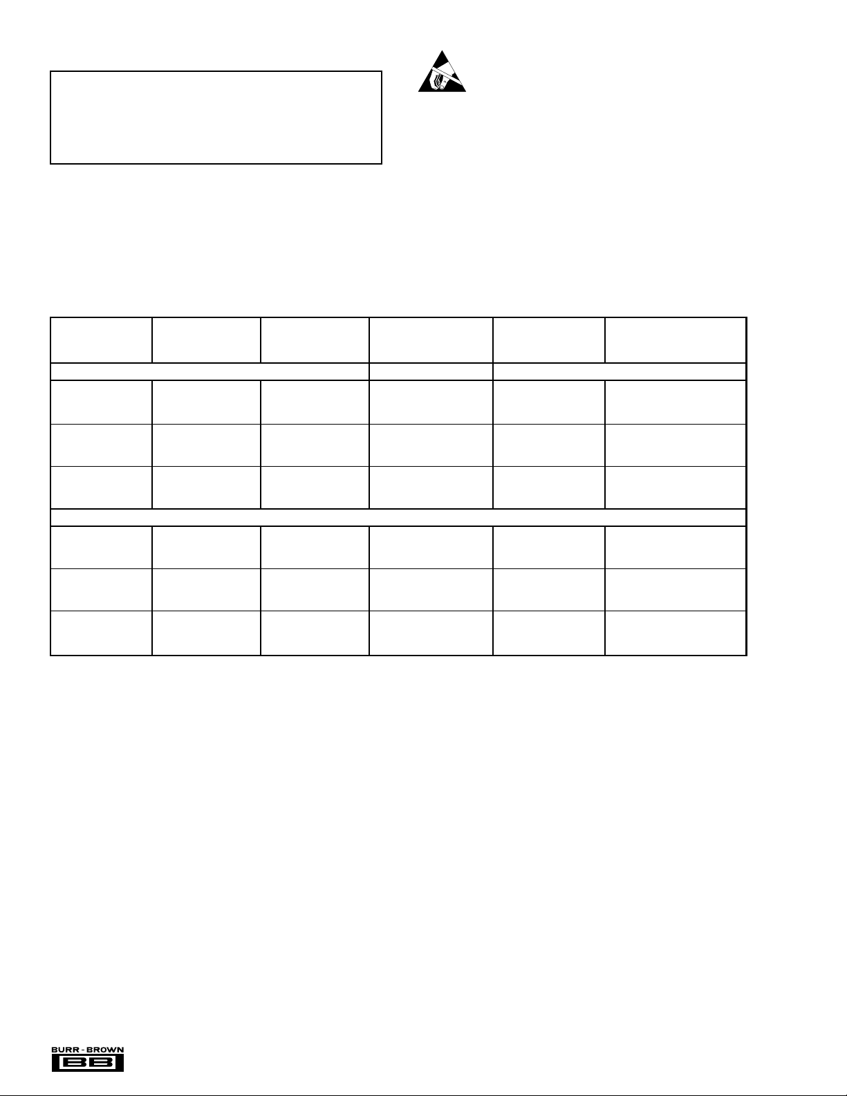
ELECTROSTATIC
DISCHARGE SENSITIVITY
This integrated circuit can be damaged by ESD. Burr-Brown
recommends that all integrated circuits be handled with
appropriate precautions. Failure to observe proper handling
and installation procedures can cause damage.
ESD damage can range from subtle performance degradation to complete device failure. Precision integrated circuits
may be more susceptible to damage because very small
parametric changes could cause the device not to meet its
published specifications.
PACKAGE/ORDERING INFORMATION
PRODUCT VOLTAGE RANGE PACKAGE NUMBER
SPECIFIED VOLTAGE DRAWING TEMPERATURE
OPA241 SERIES
Single
OPA241PA 2.7V to 5V 2.7V to 36V 8-Pin DIP 006 –40°C to +85°C
OPA241UA 2.7V to 5V 2.7V to 36V SO-8 Surface Mount 182 –40°C to +85°C
Dual
OPA2241PA 2.7V to 5V 2.7V to 36V 8-Pin DIP 006 –40°C to +85°C
OPA2241UA 2.7V to 5V 2.7V to 36V SO-8 Surface Mount 182 –40°C to +85°C
Quad
OPA4241PA 2.7V to 5V 2.7V to 36V 14-Pin DIP 010 –40°C to +85°C
OPA4241UA 2.7V to 5V 2.7V to 36V SO-14 Surface Mount 235 –40°C to +85°C
OPA251 SERIES
Single
OPA251PA ±15V 2.7V to 36V 8-Pin DIP 006 –40°C to +85°C
OPA251UA ±15V 2.7V to 36V SO-8 Surface Mount 182 –40°C to +85°C
Dual
OPA2251PA ±15V 2.7V to 36V 8-Pin DIP 006 –40°C to +85°C
OPA2251UA ±15V 2.7V to 36V SO-8 Surface Mount 182 –40°C to +85°C
Quad
OPA4251PA ±15V 2.7V to 36V 14-Pin DIP 010 –40°C to +85°C
OPA4251UA ±15V 2.7V to 36V SO-14 Surface Mount 235 –40°C to +85°C
NOTE: (1) For detailed drawing and dimension table, please see end of data sheet, or Appendix C of Burr-Brown IC Data Book.
OPERATING PACKAGE SPECIFICATION
(1)
RANGE
®
OPA241, 2241, 4241
OPA251, 2251, 4251
4
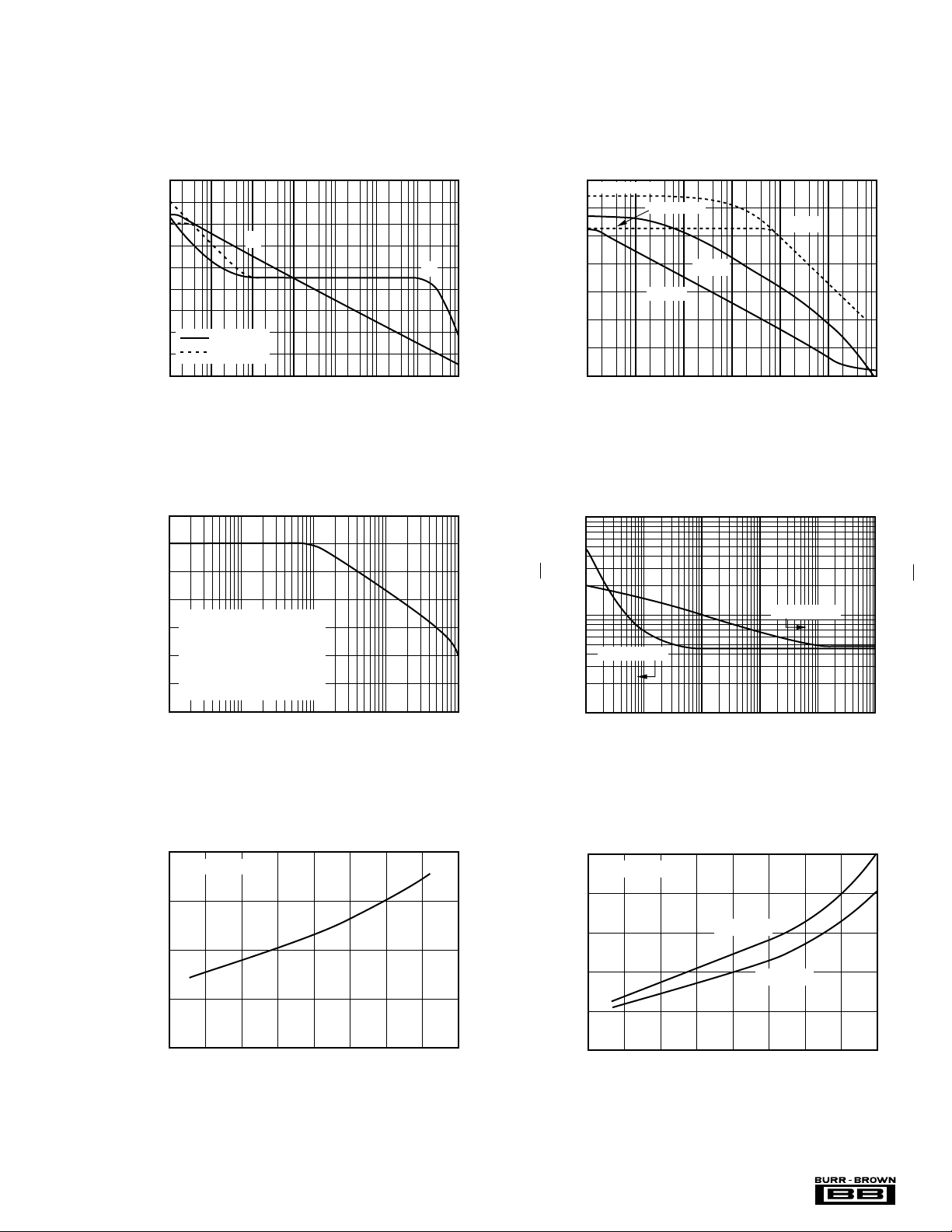
TYPICAL PERFORMANCE CURVES
At TA = +25°C, and RL = 100kΩ connected to VS/2 (ground for VS = ±15V), unless otherwise noted.
Curves apply to OPA241 and OPA251 unless specified.
160
140
120
100
80
60
40
Voltage Gain (dB)
20
0
–20
OPEN-LOOP GAIN/PHASE vs FREQUENCY
G
VS = ±15V
V
= +5V
S
0.01 0.1
1 10 100 1k 10k 100k
Frequency (Hz)
180
160
140
120
100
Φ
80
Phase (°)
60
40
20
0
140
120
100
80
60
40
20
Power Supply Rejection Ratio (dB)
0
POWER SUPPLY and COMMON-MODE
REJECTION RATIO vs FREQUENCY
VS = ±15V
VS = ±5V
CMRR
+PSRR
–PSRR
0.1 1 10 100 1k 10k 100k
Frequency (Hz)
140
130
120
110
100
90
Channel Separation (dB)
80
70
30
28
26
24
Quiescent Current (µA)
CHANNEL SEPARATION vs FREQUENCY
Dual and quad devices.
G = 1, all channels.
Quad measured channel
A to D or B to C—other
combinations yield improved
rejection.
10010 1k 10k 100k
QUIESCENT CURRENT vs SUPPLY VOLTAGE
Per Amplifier
Frequency (Hz)
INPUT VOLTAGE AND CURRENT
NOISE SPECTRAL DENSITY vs FREQUENCY
Current Noise
Voltage Noise
0.1 1 10 100 1k 10k
Frequency (Hz)
QUIESCENT CURRENT vs TEMPERATURE
Per Amplifier
VS = ±15V
VS = +5V
Voltage Noise (nV/÷Hz)
Quiescent Current (µA)
1k
100
10
40
35
30
25
20
1k
100
Current Noise (fA/√Hz)
10
22
0 5 10 15 20 25 30 35 40
Total Supply Voltage (V)
15
–75 –50 –25 0 25 50 75 100 125
Temperature (°C)
5
OPA251, 2251, 4251
OPA241, 2241, 4241
®
 Loading...