

Burr Brown INA2133UA-2K5, INA2133UA, INA133U-2K5, INA133U, INA2133U-2K5 Datasheet
...
©1999 Burr-Brown Corporation PDS-1530A Printed in U.S.A. June, 1999
®
FEATURES
● DESIGNED FOR LOW COST
● SINGLE, DUAL VERSIONS
● LOW OFFSET VOLTAGE DRIFT:
±450µV max, ±5µV/°C max
● LOW GAIN ERROR: 0.05% max
● WIDE BANDWIDTH: 1.5MHz
● HIGH SLEW RATE: 5V/µs
● FAST SETTLING TIME: 5.5µs to 0.01%
● LOW QUIESCENT CURRENT: 950µA
● WIDE SUPPLY RANGE: ±2.25V to ±18V
● SO-8 and SO-14 PACKAGES
APPLICATIONS
● DIFFERENTIAL INPUT AMPLIFIER
BUILDING BLOCK
● DIFF IN / DIFF OUT AMPLIFIER
● UNITY-GAIN INVERTING AMPLIFIER
● GAIN = +1/2 OR G = +2 AMPLIFIER
● SUMMING AMPLIFIER
● SYNCHRONOUS DEMODULATOR
● CURRENT/DIFFERENTIAL LINE RECEIVER
● VOLTAGE-CONTROLLED CURRENT SOURCE
● BATTERY POWERED SYSTEMS
● LOW COST AUTOMOTIVE
DESCRIPTION
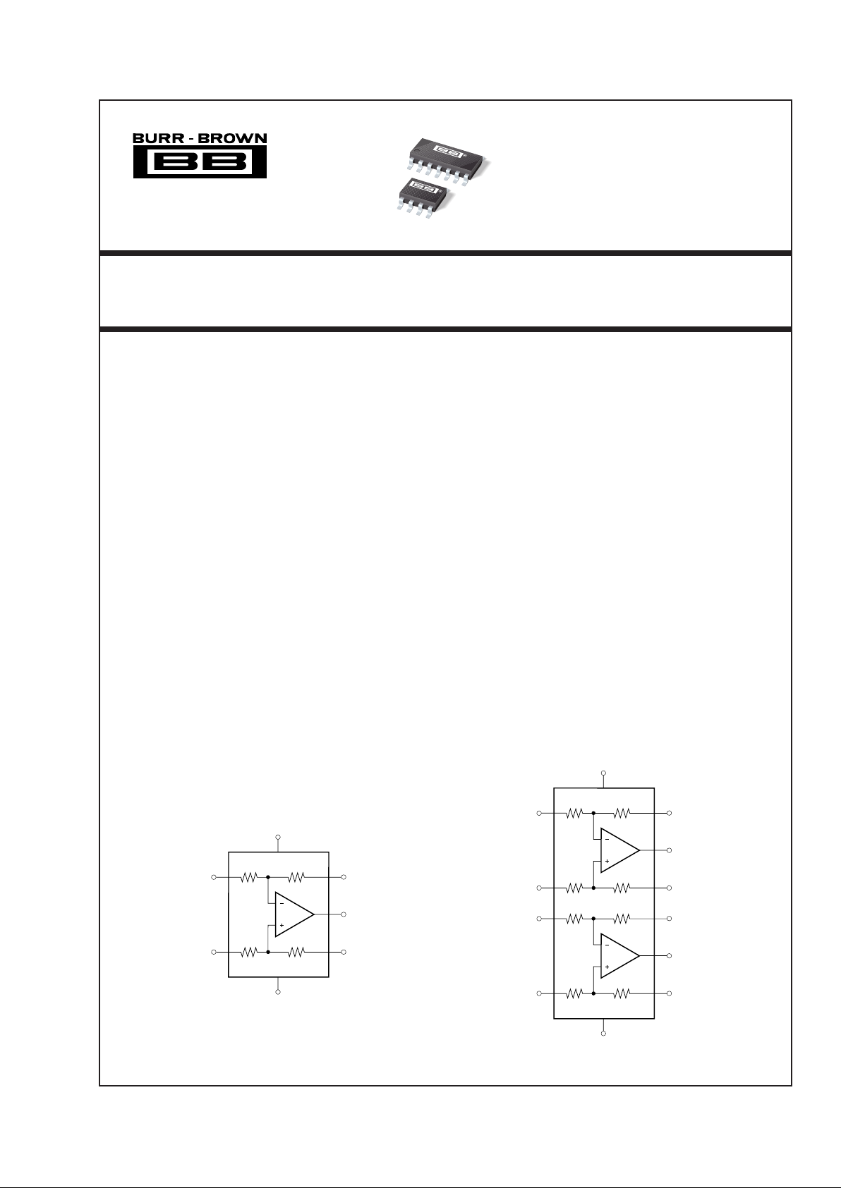
The INA133 and INA2133 are high slew rate, unitygain difference amplifiers consisting of a precision op
amp with a precision resistor network. The on-chip
resistors are laser trimmed for accurate gain and high
common-mode rejection. Excellent TCR tracking of the
resistors maintains gain accuracy and common-mode
rejection over temperature. They operate over a wide
supply range, ±2.25V to ±18V (+4.5V to +36V single
supply), and input common-mode voltage range extends
beyond the positive and negative supply rails.
INA133
INA2133
High-Speed, Precision
DIFFERENCE AMPLIFIERS
International Airport Industrial Park • Mailing Address: PO Box 11400, Tucson, AZ 85734 • Street Address: 6730 S. Tucson Blvd., Tucson, AZ 85706 • Tel: (520) 746-1111
Twx: 910-952-1111 • Internet: http://www.burr-brown.com/ • Cable: BBRCORP • Telex: 066-6491 • FAX: (520) 889-1510 • Immediate Product Info: (800) 548-6132
The differential amplifier is the foundation of many
commonly used circuits. The low cost INA133 and
INA2133 provide this precision circuit function without
using an expensive precision network.
The single version, INA133, package is the SO-8 surface
mount. The dual version, INA2133, package is the SO-14
surface mount. Both are specified for operation over the
extended industrial temperature range, –40°C to +85°C.
Operation is from –55°C to +125°C.
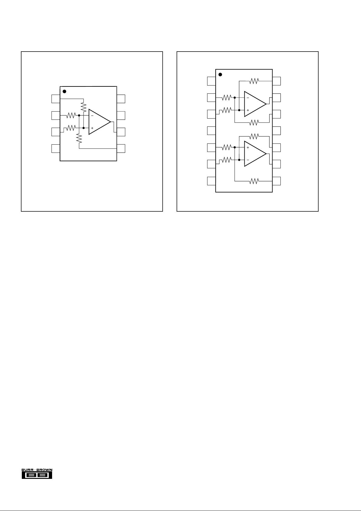
25kΩ 25kΩ
Sense
INA133
Output
V+
Ref
–In
+In
5
6
1
2
7
V–
4
3
25kΩ 25kΩ
Sense A
INA2133
Out A
V+
Ref A
–In A
+In A
12
13
14
2
11
V–
4
3
25kΩ 25kΩ
25kΩ 25kΩ
25kΩ 25kΩ
25kΩ 25kΩ
B
A
Sense B
Out B
Ref B
–In B
+In B
10
9
8
6
5
IN
A
13
3
IN
A2133
For most current data sheet and other product
information, visit www.burr-brown.com
2
®
INA133, INA2133
INA133U INA133UA
INA2133U INA2133UA
SPECIFICATIONS: VS = ±15V
At TA = +25°C, VS = ±15V, RL = 10kΩ connected to ground, and reference pin connected to ground, unless otherwise noted.
The information provided herein is believed to be reliable; however, BURR-BROWN assumes no responsibility for inaccuracies or omissions. BURR-BROWN assumes
no responsibility for the use of this information, and all use of such information shall be entirely at the user’s own risk. Prices and specifications are subject to change
without notice. No patent rights or licenses to any of the circuits described herein are implied or granted to any third party. BURR-BROWN does not authorize or warrant
any BURR-BROWN product for use in life support devices and/or systems.
PARAMETER CONDITIONS MIN TYP MAX MIN TYP MAX UNITS
OFFSET VOLTAGE
(1)
RTO
Initial
(1)
VCM = 0V ±150 ±450 ✻ ±900 µV
vs Temperature T
A
= –40°C to +85°C ±2 ±5 See Typical Curve µV/°C
vs Power Supply V
S
= ±2.25V to ±18V ±10 ±30 900 ±50 µV/V
vs Time 0.3 ✻ µV/√mo
Channel Separation (dual) dc 120 ✻ dB
INPUT IMPEDANCE
(2)
Differential 50 ✻ kΩ
Common-Mode V
CM
= 0V 25 ✻ kΩ
INPUT VOLTAGE RANGE
Common-Mode Voltage Range
Positive VO = 0V
2(V+) –3 2(V+) –2
✻✻ V
Negative V
O
= 0V
2(V–) +3 2(V–) +2
✻✻ V
Common-Mode Rejection Ratio
VCM = –27V to +27V, RS = 0Ω
80 90 74 ✻ dB
OUTPUT VOLTAGE NOISE
(3)
RTO
f = 0.1Hz to 10Hz 2 ✻ µVp-p
f = 10Hz 80 ✻ nV/√Hz
f = 100Hz 60 ✻ nV/√Hz
f = 1kHz 57 ✻ nV/√Hz
GAIN
Initial 1 ✻ V/V
Error V
O
= –14V to +13.5V ±0.02 ±0.05 ✻ ±0.1 %
vs Temperature T
A
= –40°C to +85°C ±1 ±10 ✻✻ppm/°C
Nonlinearity V
O
= –14V to +13.5V ±0.0001 ±0.001 ✻ ±0.002 % of FS
OUTPUT
Voltage Output Gain Error < 0.1%
Positive R
L
= 10kΩ to Ground (V+) –1.5 (V+)–1.3 ✻✻ V
Negative R
L
= 10kΩ to Ground (V–) +1 (V–)+0.8 ✻✻ V
Positive R
L
= 100kΩ to Ground (V+)–0.8 ✻ V
Negative R
L
= 100kΩ to Ground (V–)+0.3 ✻ V
Current Limit,
Continuous-to-Common
–25 /+32 ✻ mA
Capacitive Load (stable operation) 1000 ✻ pF
FREQUENCY RESPONSE
Small-Signal Bandwidth –3dB 1.5 ✻ MHz
Slew Rate 5 ✻ V/µs
Settling Time: 0.1% 10V Step, C
L
= 100pF 4 ✻ µs
0.01% 10V Step, C
L
= 100pF 5.5 ✻ µs
Overload Recovery Time 50% Overdrive 4 ✻ µs
POWER SUPPLY
Rated Voltage ±15 ✻ V
Operating Voltage Range
Dual Supplies ±2.25 ±18 ✻✻V
Single Supply +4.5 +36 ✻✻V
Quiescent Current (per amplifier) I
O
= 0 ±0.95 ±1.2 ✻✻mA
TEMPERATURE RANGE
Specification –40 +85 ✻✻°C
Operation –55 +125 ✻✻°C
Storage –55 +125 ✻✻°C
Thermal Resistance
θ
JA
SO-8 Surface Mount 150 ✻ °C/W
SO-14 Surface Mount 100 ✻ °C/W
✻ Specifications the same as INA133U, INA2133U.
NOTES: (1) Includes the effects of amplifier’s input bias and offset currents. (2) 25kΩ resistors are ratio matched but have ±20% absolute value. (3) Includes effects
of amplifier’s input current noise and thermal noise contribution of resistor network.
3
®
INA133, INA2133
INA133U INA133UA
INA2133U INA2133UA
SPECIFICATIONS: VS = ±5V
At TA = +25°C, VS = ±5V, RL = 10kΩ connected to ground, and reference pin connected to ground, unless otherwise noted.
Supply Voltage, V+ to V– .................................................................... 36V
Input Voltage Range ........................................................................ 2 • V
S
Output Short-Circuit (to ground)
(2)
.......................................... Continuous
Operating Temperature .................................................. –55 °C to +125°C
Storage Temperature ..................................................... –55°C to +125°C
Junction Temperature .................................................................... +150°C
Lead Temperature (soldering, 10s) ............................................... +300°C
NOTES: (1) Stresses above these ratings may cause permanent damage.
Exposure to absolute maximum conditions for extended periods may degrade
device reliability. (2) One channel per package.
ABSOLUTE MAXIMUM RATINGS
(1)
ELECTROSTATIC
DISCHARGE SENSITIVITY
This integrated circuit can be damaged by ESD. Burr-Brown
recommends that all integrated circuits be handled with appropriate precautions. Failure to observe proper handling and
installation procedures can cause damage.
ESD damage can range from subtle performance degradation
to complete device failure. Precision integrated circuits may
be more susceptible to damage because very small parametric
changes could cause the device not to meet its published
specifications.
PACKAGE SPECIFIED
DRAWING TEMPERATURE PACKAGE ORDERING TRANSPORT
PRODUCT PACKAGE NUMBER
(1)
RANGE MARKING NUMBER
(2)
MEDIA
Single
INA133U SO-8 Surface Mount 182 –40°C to +85°C INA133U INA133U Rails
"""""INA133U/2K5 Tape and Reel
INA133UA SO-8 Surface Mount 182 –40°C to +85°C INA133UA INA133UA Rails
"""""INA133UA/2K5 Tape and Reel
Dual
INA2133U SO-14 Surface Mount 235 –40°C to +85°C INA2133U INA2133U Rails
"""""INA2133U/2K5 Tape and Reel
INA2133UA SO-14 Surface Mount 235 –40°C to +85°C INA2133UA INA2133UA Rails
"""""INA2133UA/2K5 Tape and Reel
NOTES: (1) For detailed drawing and dimension table, please see end of data sheet, or Appendix C of Burr-Brown IC Data Book. (2) Models with a slash (/ ) are
available only in Tape and Reel in the quantities indicated (e.g., /2K5 indicates 2500 devices per reel). Ordering 2500 pieces of “INA133UA/2K5” will get a single
2500-piece Tape and Reel. For detailed Tape and Reel mechanical information, refer to Appendix B of Burr-Brown IC Data Book.
PACKAGE/ORDERING INFORMATION
PARAMETER CONDITIONS MIN TYP MAX MIN TYP MAX UNITS
OFFSET VOLTAGE
(1)
RTO
Initial
(1)
VCM = 0V ±300 ±750 ✻ ±1500 µV
vs Temperature ±2 ✻ µV/°C
INPUT VOLTAGE RANGE
Common-Mode Voltage Range
Positive VO = 0V
2(V+) – 3 2(V+) – 2
✻✻ V
Negative V
O
= 0V
2(V–) +3 2(V–) + 2
✻✻ V
Common-Mode Rejection Ratio
VCM = –7V to +7V, RS = 0Ω
80 90 74 ✻ dB
GAIN
Initial 1 ✻ V/V
Gain Error V
O
= –4V to 3.5V ±0.02 ±0.05 ✻ ±0.1 %
Nonlinearity V
O
= –4V to 3.5V ±0.0001 ±0.001 ✻ ±0.002 % of FS
OUTPUT
Voltage Output Gain Error < 0.1%
Positive R
L
= 10kΩ to Ground (V+) –1.5 (V+) –1.3 ✻✻ V
Negative R
L
= 10kΩ to Ground (V–) +1 (V–) +0.8 ✻✻ V
Positive R
L
= 100kΩ to Ground (V+) –0.8 ✻ V
Negative R
L
= 100kΩ to Ground (V–) +0.3 ✻ V
POWER SUPPLY
Rated Voltage ±15 ✻ V
Operating Voltage Range
Dual Supplies ±2.25 ±18 ✻✻V
Single Supply +4.5 +36 ✻✻V
Quiescent Current (per amplifier) I
O
= 0 ±0.92 ±1.2 ✻✻mA
✻ Specifications the same as INA133U, INA2133U.
NOTES: (1) Includes the effects of amplifier’s input bias and offset currents.
4
®
INA133, INA2133
PIN CONFIGURATIONS
Top View SO-8 Top View SO-14
Ref
–In
+In
V–
NC
V+
Output
Sense
NC = No Connection
INA133
1
2
3
4
8
7
6
5
NC
–In A
+In A
V–
+In B
–In B
NC
Ref A
Out A
Sense A
V+
Sense B
Out B
Ref B
NC = No Connection
1
2
3
4
5
6
7
14
13
12
11
10
9
8
A
B
INA2133
5
®
INA133, INA2133
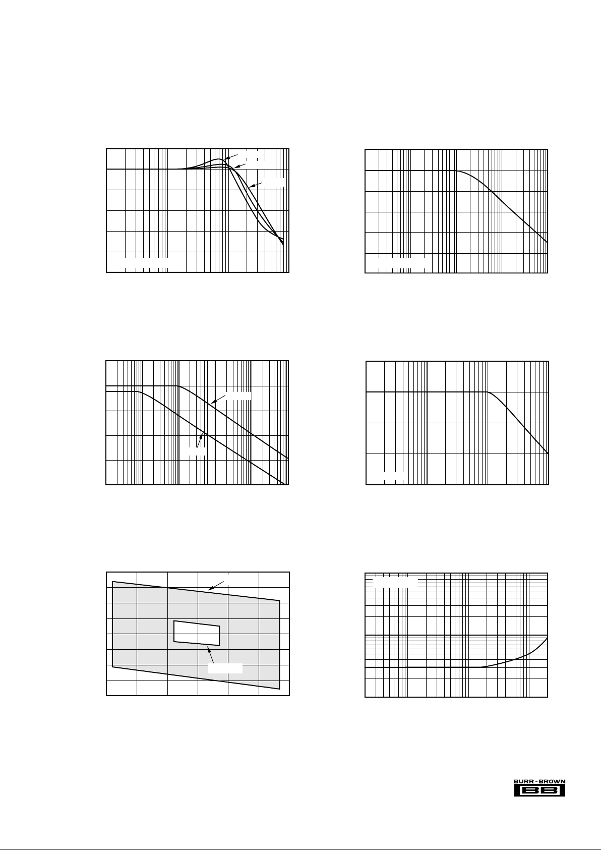
TYPICAL PERFORMANCE CURVES
At TA = +25°C, VS = ±15V, RL = 10kΩ connected to ground, and reference pin connected to ground, unless otherwise noted.
GAIN vs FREQUENCY
Frequency (Hz)
Closed-Loop Gain (dB)
10k 1M100k 10M
10
0
–10
–20
–30
–40
–50
VS = ±15V or ±5V
+125°C
+25°C
–55°C
COMMON-MODE REJECTION vs FREQUENCY
Frequency (Hz)
Common-Mode Rejection (dB)
100 100k1k 10k 1M
100
90
80
70
60
50
40
VS = ±15V or ±5V
POWER SUPPLY REJECTION vs FREQUENCY
Frequency (Hz)
Power Supply Rejection (dB)
1 100 1k 10k10 100k
120
100
80
60
40
20
–PSRR
+PSRR
CHANNEL SEPARATION vs FREQUENCY
Channel Separation (dB)
Frequency (Hz)
130
120
110
100
90
100 1k 10k 100k
INA2133
INPUT COMMON-MODE VOLTAGE
vs OUTPUT VOLTAGE
Output Voltage (V)
Common-Mode Voltage (V)
–15 0 5 10–5–10 15
40
30
20
10
0
–10
–20
–30
–40
VS = ±5V
VS = ±15V
TOTAL HARMONIC DISTORTION+NOISE
vs FREQUENCY
Frequency (Hz)
THD+N (%)
20 1k 10k100 20k
0.1
0.01
0.001
500kHz Filter
 Loading...