

BURR-BROWN INA163 User Manual
SBOS177D – NOVEMBER 2000 – REVISED MAY 2005
Low-Noise, Low-Distortion
INSTRUMENTATION AMPLIFIER
INA163
FEATURES
● LOW NOISE: 1nV/√Hz at 1kHz
● LOW THD+N: 0.002% at 1kHz, G = 100
● WIDE BANDWIDTH: 800kHz at G = 100
● WIDE SUPPLY RANGE: ±4.5V to ±18V
● HIGH CMR: > 100dB
● GAIN SET WITH EXTERNAL RESISTOR
● SO-14 SURFACE-MOUNT PACKAGE
APPLICATIONS
● PROFESSIONAL MICROPHONE PREAMPS
● MOVING-COIL TRANSDUCER AMPLIFIERS
● DIFFERENTIAL RECEIVERS
● BRIDGE TRANSDUCER AMPLIFIERS
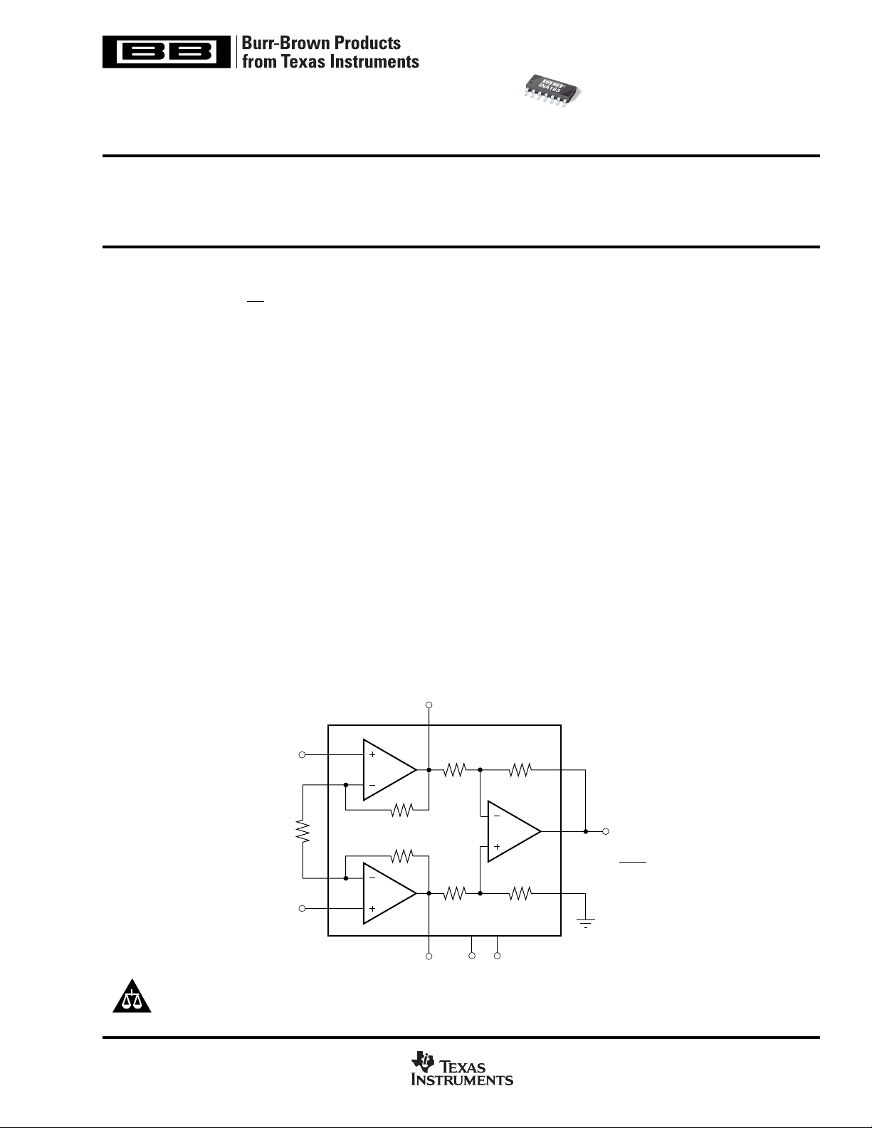
4
V
IN−
3
A1
3kΩ
1
V
O
1
6kΩ 6kΩ
DESCRIPTION
The INA163 is a very low-noise, low-distortion, monolithic instrumentation amplifier. Its current-feedback
circuitry achieves very wide bandwidth and excellent
dynamic response over a wide range of gain. It is ideal
for low-level audio signals such as balanced lowimpedance microphones. Many industrial, instrumentation, and medical applications also benefit from its
low noise and wide bandwidth.
Unique distortion cancellation circuitry reduces distortion to extremely low levels, even in high gain. The
INA163 provides near-theoretical noise performance
for 200Ω source impedance. Its differential input, low
noise, and low distortion provide superior performance
in professional microphone amplifier applications.
The INA163’s wide supply voltage, excellent output
voltage swing, and high output current drive allow its
use in high-level audio stages as well.
The INA163 is available in a space-saving SO-14
surface-mount package, specified for operation over
the –40°C to +85°C temperature range.
INA163
Sense
8
R
G
12
V
IN+
5
Please be aware that an important notice concerning availability, standard warranty, and use in critical applications of
Texas Instruments semiconductor products and disclaimers thereto appears at the end of this data sheet.
All trademarks are the property of their respective owners.
PRODUCTION DATA information is current as of publication date.
Products conform to specifications per the terms of Texas Instruments
standard warranty. Production processing does not necessarily include
testing of all parameters.
A2
3kΩ
6kΩ 6kΩ
14 11 6
V
2
V+ V−
O
www.ti.com
A3
V
G = 1 +
O
6000
R
G
9
Ref
10
Copyright © 2000–2005, Texas Instruments Incorporated
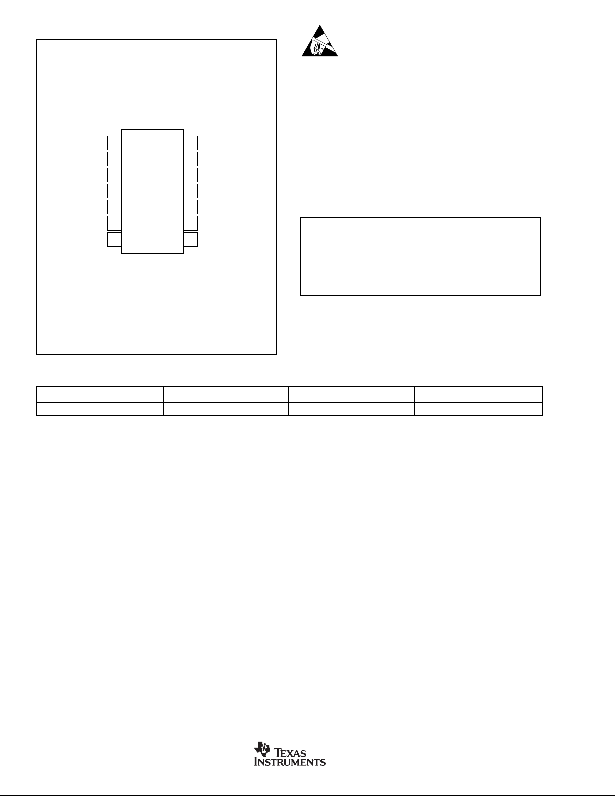
PIN CONFIGURATION
Top View
1
1
V
O
2
NC
3
GS1
4
V
IN−
5
V
IN+
6
V−
7
NC
NC = No Internal Connection
14
VO2
13
NC
12
GS2
11
V+
10
Ref
9
V
O
8
Sense
PACKAGE/ORDERING INFORMATION
ELECTROSTATIC
DISCHARGE SENSITIVITY
This integrated circuit can be damaged by ESD. Texas
Instruments recommends that all integrated circuits be
handled with appropriate precautions. Failure to observe proper handling and installation procedures can
cause damage.
ESD damage can range from subtle performance degradation to complete device failure. Precision integrated
circuits may be more susceptible to damage because
very small parametric changes could cause the device
not to meet its published specifications.
ABSOLUTE MAXIMUM RATINGS
Power Supply Voltage ....................................................................... ±18V
Signal Input Terminals, Voltage
Output Short-Circuit to Ground ............................................... Continuous
Operating Temperature .................................................. –55°C to +125°C
Storage Temperature ..................................................... –55°C to +125°C
Junction Temperature .................................................................... +150°C
Lead Temperature (soldering, 10s) ............................................... +300°C
NOTES: (1) Stresses above these ratings may cause permanent damage.
Exposure to absolute maximum conditions for extended periods may degrade
device reliability. These are stress ratings only, and functional operation of the
device at these or any other conditions beyond those specified is not implied.
(2) Input terminals are diode-clamped to the power-supply rails. Input signals
that can swing more than 0.5V beyond the supply rails should be current
limited to 10mA or less.
(1)
Current
(2)
.................. (V–) – 0.5V to (V+) + 0.5V
(2)
.................................................... 10mA
(1)
PRODUCT PACKAGE-LEAD DESIGNATOR MARKING
INA163UA SO-14 Surface Mount D INA163UA
NOTE: (1) For the most current package and ordering information, see the Package Option Addendum located at the end of this document, or see the TI web site
at www.ti.com.
INA163
2
www.ti.com
SBOS177D
ELECTRICAL CHARACTERISTICS: VS = ±15V
TA = +25°C and at rated supplies, VS = ±15V, RL = 2kΩ connected to ground, unless otherwise noted.
INA163UA
PARAMETER CONDITIONS MIN TYP MAX UNITS
GAIN
Range 1 to 10000 V/V
Gain Equation
Gain Error, G = 1 ±0.1 ±0.25 %
Gain Temp Drift Coefficient, G = 1 ±1 ±10 ppm/°C
Nonlinearity, G = 1 ±0.0003 % of FS
INPUT STAGE NOISE
Voltage Noise R
f
= 1kHz 1nV/√Hz
O
f
= 100Hz 1.2 nV/√Hz
O
f
= 10Hz 2nV/√Hz
O
Current Noise
f
= 1kHz 0.8 pA/√Hz
O
OUTPUT STAGE NOISE
Voltage Noise, f
INPUT OFFSET VOLTAGE
Input Offset Voltage V
vs Temperature T
vs Power Supply V
INPUT VOLTAGE RANGE
Common-Mode Voltage Range V
Common-Mode Rejection, G = 1 V
INPUT BIAS CURRENT
Initial Bias Current 212µA
vs Temperature 10 nA/°C
Initial Offset Current 0.1 1 µA
vs Temperature 0.5 nA/°C
INPUT IMPEDANCE
DYNAMIC RESPONSE
Bandwidth, Small Signal, –3dB, G = 1 3.4
Slew Rate 15 V/µs
THD+Noise, f = 1kHz G = 100 0.002 %
Settling Time, 0.1% G = 100, 10V Step 2 µs
Overload Recovery 50% Overdrive 1 µs
OUTPUT
Voltage R
Load Capacitance Stability 1000 pF
Short-Circuit Current Continuous-to-Common ±60 mA
POWER SUPPLY
Rated Voltage ±15 V
Voltage Range ±4.5 ±18 V
Current, Quiescent I
TEMPERATURE RANGE
Specification –40 +85 °C
Operating –40 +125 °C
θ
JA
NOTE: (1) Gain accuracy is a function of external R
(1)
G = 1 + 6k/R
G
G = 10 ±0.2 ±0.7 %
G = 100 ±0.2 %
G = 1000 ±0.5 %
G > 10 ±25 ±100 ppm/°C
G = 100 ±0.0006 % of FS
= 0Ω
SOURCE
= 1kHz 60 nV/√Hz
O
= V
CM
= T
A
= ±4.5V to ±18V 1 + 50/G 3 + 200/G µV/V
S
IN+
V
IN+
= ±11V, R
G = 100 100 116 dB
CM
= 0V 50 + 2000/G 250 + 5000/G µV
OUT
to T
MIN
MAX
– V
= 0V (V+) – 4 (V+) – 3V
IN–
– V
= 0V (V–) + 4 (V–) + 3 V
IN–
= 0Ω 70 80 dB
SRC
1 + 20/G µV/°C
Differential 60 2MΩ pF
Common-Mode 60 2MΩ pF
G = 100 800 kHz
0.01% G = 100, 10V Step 3.5 µs
= 2kΩ to Gnd (V+) – 2 (V+) – 1.8 V
L
= 0mA ±10 ±12 mA
O
(V–) + 2 (V–) + 1.8 V
100 °C/W
.
G
INA163
SBOS177D
www.ti.com
3
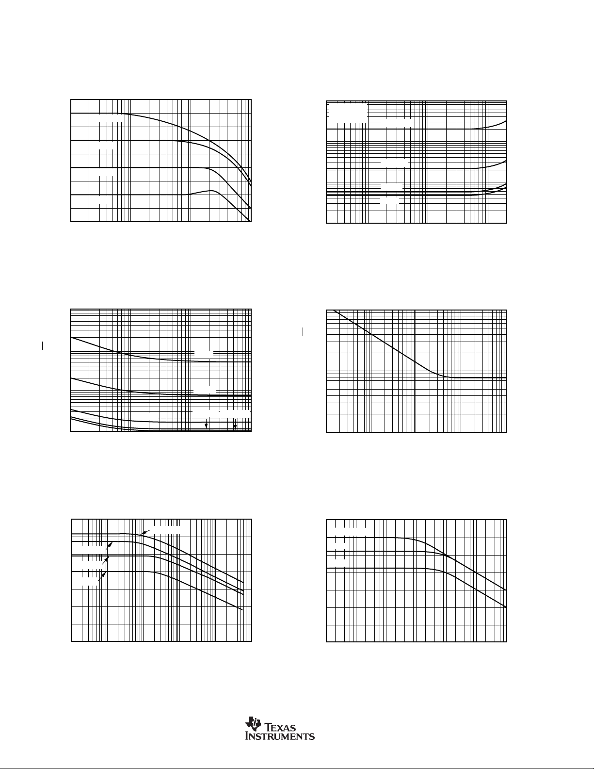
TYPICAL CHARACTERISTICS
0.1
0.01
0.001
0.0001
THD+N (%)
THD+N vs FREQUENCY
Frequency (Hz)
20 100 1k 10k 20k
VO = 5Vrms
R
L
= 10kΩ
G = 10
G = 1
G = 100
G = 1000
At TA = +25°C, VS = 5V, VCM = 1/2 VS, RL = 25kΩ, CL = 50pF, unless otherwise noted.
70
60
50
40
30
20
Gain (dB)
10
0
−10
−20
1k
100
G = 1000
G = 100
G = 10
10k 100k 1M 10M
GAIN vs FREQUENCY
G = 1
Frequency (Hz)
NOISE VOLTAGE (RTI) vs FREQUENCY
G = 1
10
1
CURRENT NOISE SPECTRAL DENSITY
10
Noise (RTI) (nV/√Hz)
1
140
120
100
80
60
40
Input Referred CMR (dB)
20
G = 10
G = 500
G = 100
10 100 1k 10k
Frequency (Hz)
COMMON- MODE REJECTION vs FREQUENCY
G = 1000
G = 100
G = 10
G = 1
0
10 1M100 1k 10k 100k
Frequency (Hz)
G = 1000
Current Noise Density (pA/√Hz)
0.1
1 10 100 1k 10k
Frequency (Hz)
140
120
100
Power-Supply Rejection (dB)
POWER-SUPPLY REJECTION vs FREQUENCY
G = 100, 1000
G = 10
G = 1
80
60
40
20
0
11M10 100 1k 10k 100k
Frequency (Hz)
4
www.ti.com
INA163
SBOS177D
TYPICAL CHARACTERISTICS (Cont.)
SETTLING TIME vs GAIN
Settling Time (µs)
Gain
1 10 100 1000
10
8
6
4
2
0
20V Step
0.01%
0.1%
SMALL-SIGNAL TRANSIENT RESPONSE
(G = 100)
20mV/div
10µs/div
LARGE-SIGNAL TRANSIENT RESPONSE
(G = 100)
5V/div
2.5µs/div
At TA = +25°C, VS = 5V, VCM = 1/2 VS, RL = 25kΩ, CL = 50pF, unless otherwise noted.
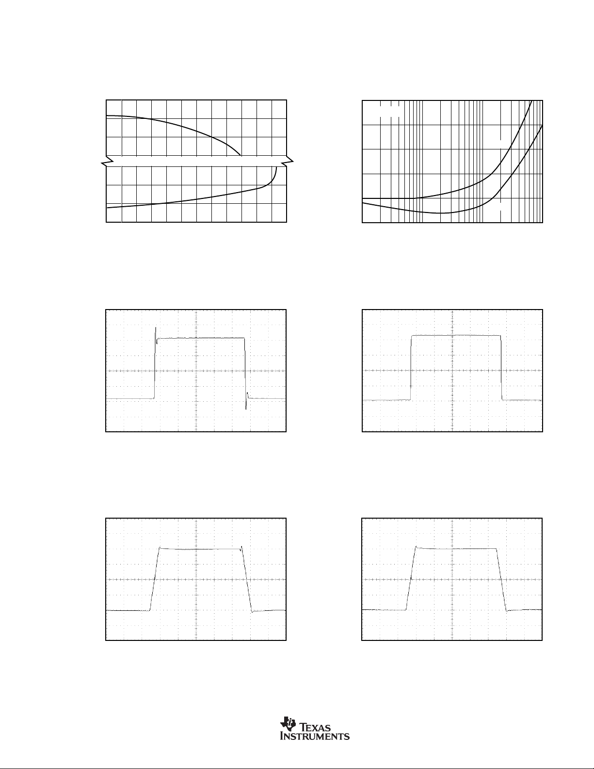
OUTPUT VOLTAGE SWING vs OUTPUT CURRENT
V+
(V+) − 2
(V+) − 4
(V+) − 6
(V−) + 6
(V−) + 4
Output Voltage to Rail (V)
(V−) + 2
V−
0 102030405060
Output Current (mA)
20mV/div
SMALL-SIGNAL TRANSIENT RESPONSE
(G = 1)
2.5µs/div
LARGE-SIGNAL TRANSIENT RESPONSE
(G = 1)
5V/div
INA163
SBOS177D
2.5µs/div
www.ti.com
5
 Loading...