

Burr Brown INA156EA, INA156EA-2K5 Datasheet
®
INA156
©1999 Burr-Brown Corporation PDS-1565A Printed in U.S.A. December, 1999
FEATURES
● RAIL-TO-RAIL OUTPUT SWING: Within 20mV
● LOW OFFSET DRIFT: ±5µV/°C
● INTERNAL FIXED GAIN = 10V/V OR 50V/V
● SPECIFIED TEMPERATURE RANGE:
–55°C to +125°C
● LOW INPUT BIAS CURRENT: 1pA
● WIDE BANDWIDTH: 550kHz in G = 10
● HIGH SLEW RATE: 6.5V/µs
● LOW COST
● TINY MSOP-8 PACKAGES
Single-Supply, Rail-to-Rail Output, CMOS
INSTRUMENTATION AMPLIFIER
DESCRIPTION
The INA156 is a low-cost CMOS instrumentation
amplifier with rail-to-rail output swing optimized for
low-voltage, single-supply operation.
Wide bandwidth (550kHz in G = 10) and high slew
rate (6.5V/µs) make the INA156 suitable for driving
sampling A/D converters as well as general purpose
and audio applications. Fast settling time allows use
with higher speed sensors and transducers, and rapid
scanning data acquisition systems.
APPLICATIONS
● INDUSTRIAL SENSOR AMPLIFIERS:
Bridge, RTD, Thermocouple, Flow, Position
● MEDICAL EQUIPMENT:
ECG, EEG, EMG Amplifiers
● DRIVING A/D CONVERTERS
● PCMCIA CARDS
● AUDIO PROCESSING
● COMMUNICATIONS
● TEST EQUIPMENT
●
LOW COST AUTOMOTIVE INSTRUMENTATION
International Airport Industrial Park • Mailing Address: PO Box 11400, Tucson, AZ 85734 • Street Address: 6730 S. Tucson Blvd., Tucson, AZ 85706 • Tel: (520) 746-1111
Twx: 910-952-1111 • Internet: http://www.burr-brown.com/ • Cable: BBRCORP • Telex: 066-6491 • FAX: (520) 889-1510 • Immediate Product Info: (800) 548-6132
For most current data sheet and other product
information, visit www.burr-brown.com
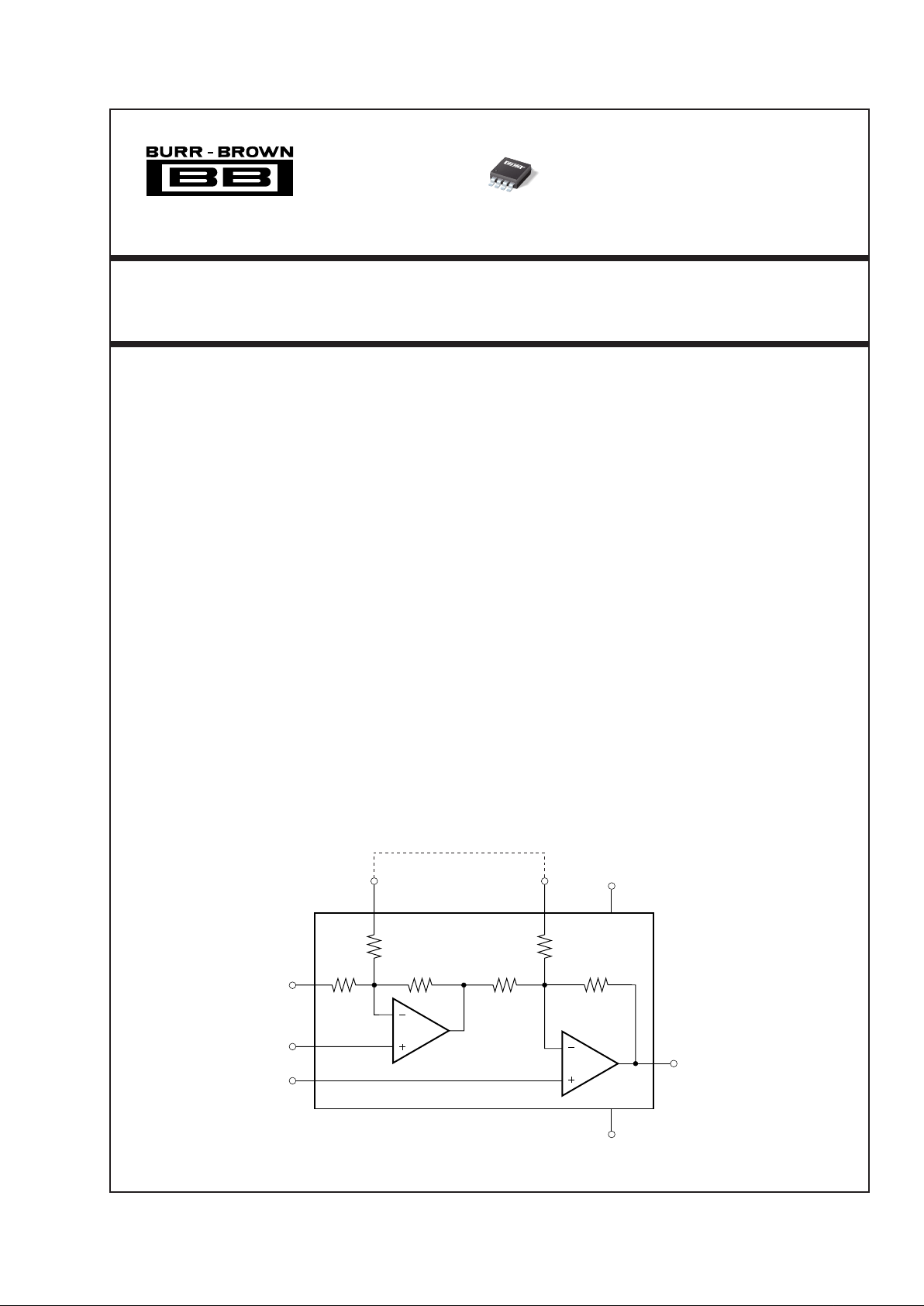
Gain can be set to 10V/V or 50V/V by pin strapping.
Gains between these two values can be obtained with
the addition of a single resistor. The INA156 is fully
specified over the supply range of +2.7V to +5.5V.
The INA156 is available in an MSOP-8 surface-mount
package specified for operation over the temperature
range –55°C to 125°C.
22.2kΩ
200kΩ
V
IN
–
V
IN
+
Ref
R
G
INA156
V
O
22.2kΩ
5kΩ5kΩ
200kΩ
R
G
V+
V–
1
5
2
3
8
7
4
6
A1
A2
G = 10 pins open
G = 50 pins connected
VO = (VIN – VIN) • G + V
REF
+–
INA156
2
®
INA156
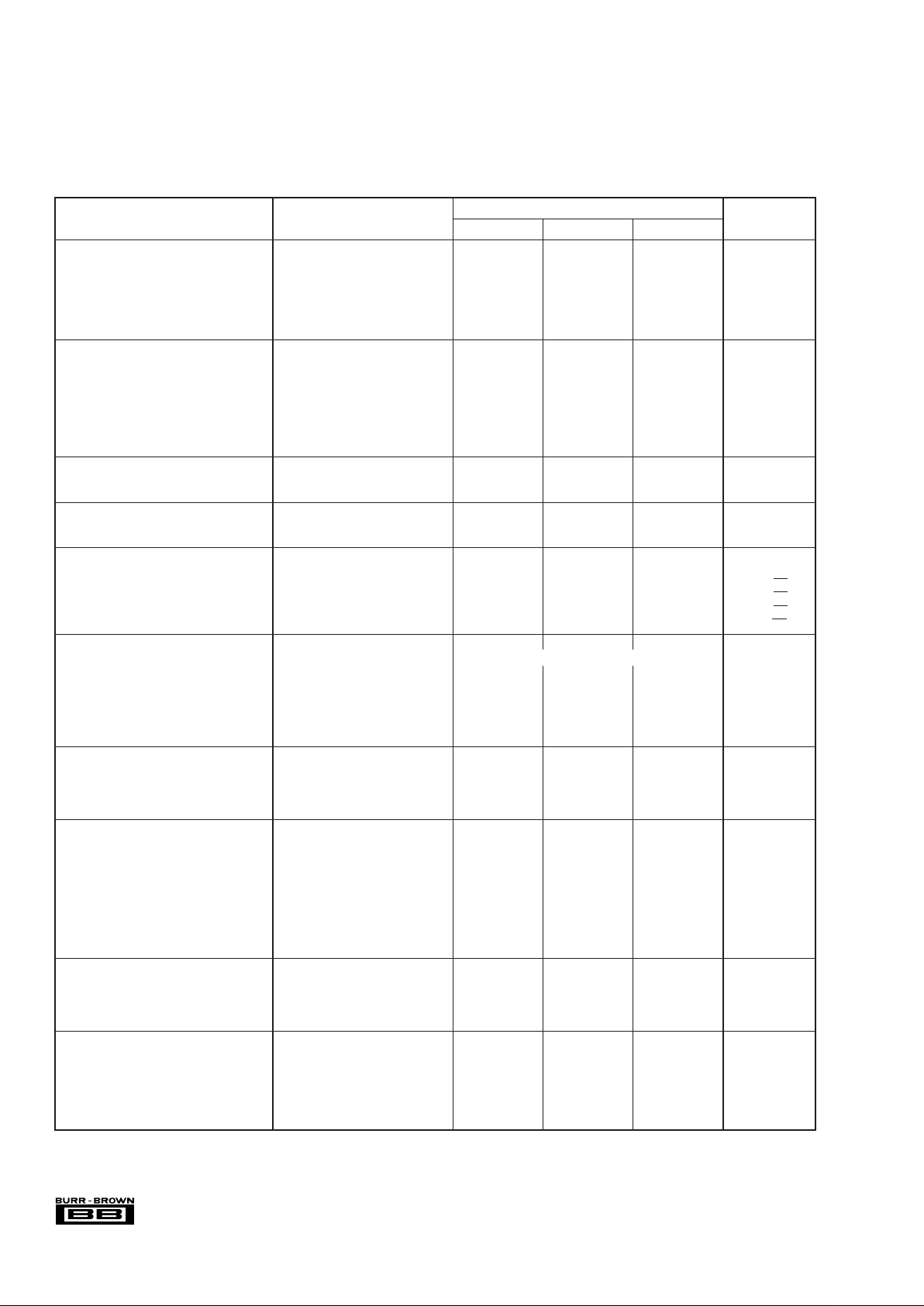
SPECIFICATIONS: VS = +2.7V to +5.5V
Boldface limits apply over the specified temperature range, TA = –55°C to +125°C
At TA = +25°C, RL = 10kΩ connected to VS/2. RG pins open (G = 10), and Ref = VS/2, unless otherwise noted.
INA156E, A
PARAMETER CONDITION MIN TYP MAX UNITS
INPUT
Offset Voltage, RTI V
OS
VS = +5.0V, V
CM
= VS/2 ±2.5 ±8mV
Over Temperature
±
9 mV
Drift dV
OS/dT
±
5 µV/°C
vs Power Supply PSRR V
S
= +2.7V to +6V, VCM = 0.2 • V
S
±50 ±200 µV/V
Over Temperature
±
250 µV/V
vs Time ±0.4 µV/mo
INPUT VOLTAGE RANGE
Safe Input Voltage (V–) – 0.5 (V+) + 0.5 V
Common-Mode Range
(1)
V
CM
VS = 5.5V 0.3 5.2
(2)
V
V
S
= 2.7V 0.2 2.5
(2)
V
Common-Mode Rejection Ratio CMRR V
S
= 5.5V, 0.6V < VCM < 3.7V, G = 10 66 78 dB
Over Temperature 65 dB
VS = 5.5V, 0.6V < VCM < 3.7V, G = 50
74 87 dB
Over Temperature 73 dB
INPUT IMPEDANCE
Differential 10
13
|| 3 Ω || pF
Common-Mode 10
13
|| 3 Ω || pF
INPUT BIAS CURRENT
Input Bias Current I
B
±1 ±10 pA
Offset Current I
OS
±1 ±10 pA
NOISE, RTI R
S
= 0Ω, G = 10 or 50
Voltage Noise: f = 0.1Hz to 10Hz 4.5 µV/Vp-p
Voltage Noise Density: f = 10Hz 260 nV/√Hz
f = 100Hz 99 nV/√Hz
f = 1kHz 40 nV/√Hz
Current Noise: f = 1kHz 2 fA/√Hz
GAIN 10 50 V/V
Gain Equation G = 10 + 400kΩ/(10kΩ + R
G
) V/V
Gain Error
(3)
VS = 5.5V, VO = 0.02V to 5.48V, G = 10
±0.08 ±0.4 %
vs Temperature
±
2
±
10 ppm/°C
VS = 5.5V, VO = 0.05V to 5.45V, G = 50 ±0.1 ±0.8
%
vs Temperature
±
15
±
30 ppm/°C
Nonlinearity
VS = 5.5V, G = 10 or 50 ±0.005 ±
0.015 % of FSR
Over Temperature
±
0.015 % of FSR
OUTPUT
Voltage Output Swing from Rail G = 10, RL = 10kΩ, G
ERR
< 0.4% 5 20 mV
Over Temperature 20 mV
Short-Circuit Current Short-Circuit to Ground ±50 mA
Capacitance Load (stable operation) See Typical Curve
FREQUENCY RESPONSE
Bandwidth, –3dB BW G = 10 550 kHz
G = 50 110 kHz
Slew Rate SR V
S
= 5.5V, CL = 100pF 6.5 V/µs
Settling Time: 0.1% t
SVS
= 5.5V, VO = 2V Step, CL = 100pF, G = 10
5 µs
VS = 5.5V, VO = 2V Step, CL = 100pF, G = 50
11 µs
0.01%
VS = 5.5V, VO = 2V Step, CL = 100pF, G = 10
8 µs
VS = 5.5V, VO = 2V Step, CL = 100pF, G = 50
15 µs
Overload Recovery 50% Input Overload 0.2 µs
Total Harmonic Distortion + Noise THD+N See Typical Curve
POWER SUPPLY
Specified Voltage Range +2.7 +5.5 V
Operating Voltage Range
+2.5 to +6
V
Quiescent Current V
IN
= 0, IO = 0 1.8 2.5 mA
Over Temperature V
IN
= 0, IO = 0 3.2 mA
TEMPERATURE RANGE
Specified Range –55 +125 °C
Operating Range –65 +150 °C
Storage Range –65 +150 °C
Thermal Resistance
θ
JA
MSOP-8 Surface Mount 150 °C/W
SO-8 Surface Mount 150 °C/W
NOTES: (1) For further information, refer to typical performance curves on common-mode input range. (2) Operation beyond (V+) – 1.8V (max) results in reduced common-mode
rejection. See discussion and Figure 6 in the text of this data sheet. (3) Does not include error and TCR of additional optional gain-setting resistor in series with R
G
, if used.
3
®
INA156
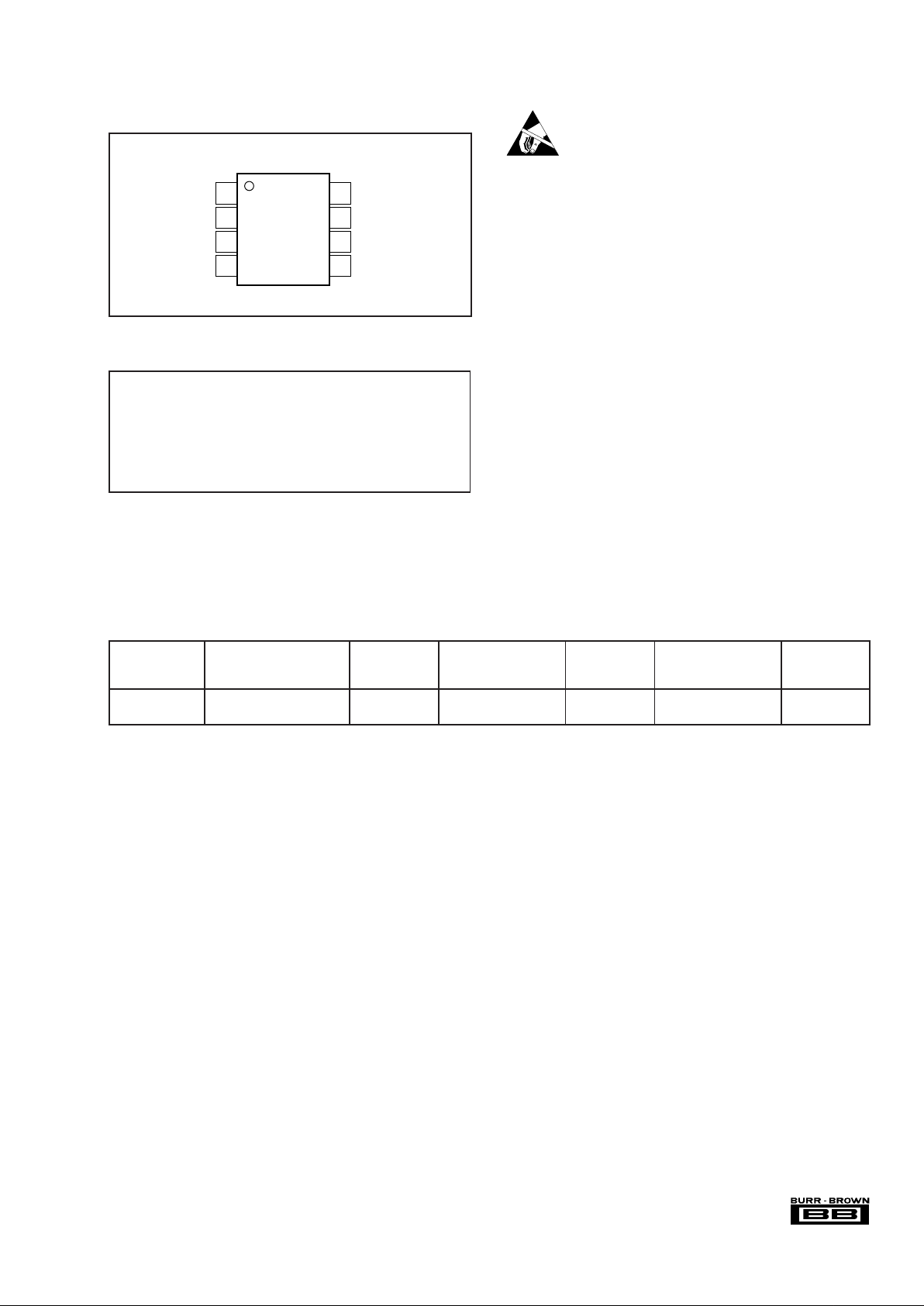
PIN CONFIGURATION
ELECTROSTATIC
DISCHARGE SENSITIVITY
This integrated circuit can be damaged by ESD. Burr-Brown
recommends that all integrated circuits be handled with
appropriate precautions. Failure to observe proper handling
and installation procedures can cause damage.
ESD damage can range from subtle performance degradation
to complete device failure. Precision integrated circuits may
be more susceptible to damage because very small parametric
changes could cause the device not to meet its published
specifications.
The information provided herein is believed to be reliable; however, BURR-BROWN assumes no responsibility for inaccuracies or omissions. BURR-BROWN assumes
no responsibility for the use of this information, and all use of such information shall be entirely at the user’s own risk. Prices and specifications are subject to change
without notice. No patent rights or licenses to any of the circuits described herein are implied or granted to any third party. BURR-BROWN does not authorize or warrant
any BURR-BROWN product for use in life support devices and/or systems.
Top View MSOP
Supply Voltage, V+ to V– ................................................................... 7.5V
Signal Input Terminals, Voltage
(2)
.................. (V–) – 0.5V to (V+) + 0.5V
Current
(2)
.................................................... 10mA
Output Short-Circuit
(3)
.............................................................. Continuous
Operating Temperature .................................................. –65°C to +150°C
Storage Temperature ..................................................... –65°C to +150°C
Junction Temperature .................................................................... +150°C
Lead Temperature (soldering, 10s) ............................................... +300°C
NOTES: (1) Stresses above these ratings may cause permanent damage.
Exposure to absolute maximum conditions for extended periods may degrade
device reliability. These are stress ratings only, and functional operation of the
device at these or any other conditions beyond those specified is not implied.
(2) Input terminals are diode-clamped to the power supply rails. Input signals
that can swing more that 0.5V beyond the supply rails should be current limited
to 10mA or less. (3) Short circuit to ground.
ABSOLUTE MAXIMUM RATINGS
(1)
PACKAGE SPECIFIED
DRAWING TEMPERATURE PACKAGE ORDERING TRANSPORT
PRODUCT PACKAGE NUMBER RANGE MARKING NUMBER
(1)
MEDIA
INA156 EA MSOP-8 337 –55°C to +125°C A56 INA156EA/250 Tape and Reel
"""""INA156EA/2K5 Tape and Reel
NOTE: (1) Models with a slash (/) are available only in Tape and Reel in the quantities indicated (e.g., /2K5 indicates 2500 devices per reel). Ordering 2500 pieces
of “INA156EA/2K5” will get a single 2500-piece Tape and Reel.
PACKAGE/ORDERING INFORMATION
R
G
V
IN
V
IN
V–
R
G
V+
V
OUT
Ref
1
2
3
4
8
7
6
5
INA156
+
–
 Loading...