

Page 1
BP2865E
Non-isolated Buck Offline LED Driver
BP2865E_EN _DS_Rev.1.0 www.bpsemi.com 1
BPS Confidential – Customer Use Only
晶丰明源半导体
Description
The BP2865E is a high precision buck constant
current LED driver. The device operates in critical
conduction mode and is suitable for 85Vac~265Vac
universal input offline LED lighting.
The BP2865E integrates a 500V power MOSFET.
With patent pending MOSFET driving technique, the
operating current of the IC is very low. So it doesn’t
need the auxiliary winding for supplying the chip. It
can achieve excellent constant current performance
with very few external components, so the system
cost and size are minimized.
The BP2865E utilizes patent pending current control
method. It can achieve precise output current and
excellent line regulation. The driver operates in
critical conduction mode, the output current does not
change with the inductance and LED output voltage.
The BP2865E offers rich protection functions to
improve the system reliability, including LED open
circuit protection, LED short circuit protection, VCC
under voltage protection, CS resistor short circuit
protection and thermal regulation function.
Features
Critical Conduction Mode Operation
Internal 500V Power MOSFET
No Auxiliary Winding
Ultra Low Operating Current
±5% LED Output Current Accuracy
LED Open Protection
LED Short Protection
Current Sensing Resistor Short Protection
VCC Under Voltage Protection
Thermal Regulation Function
Available in DIP-7 Package
Applications
LED Fluorescent Lamp
LED Bulb
Other LED Lighting
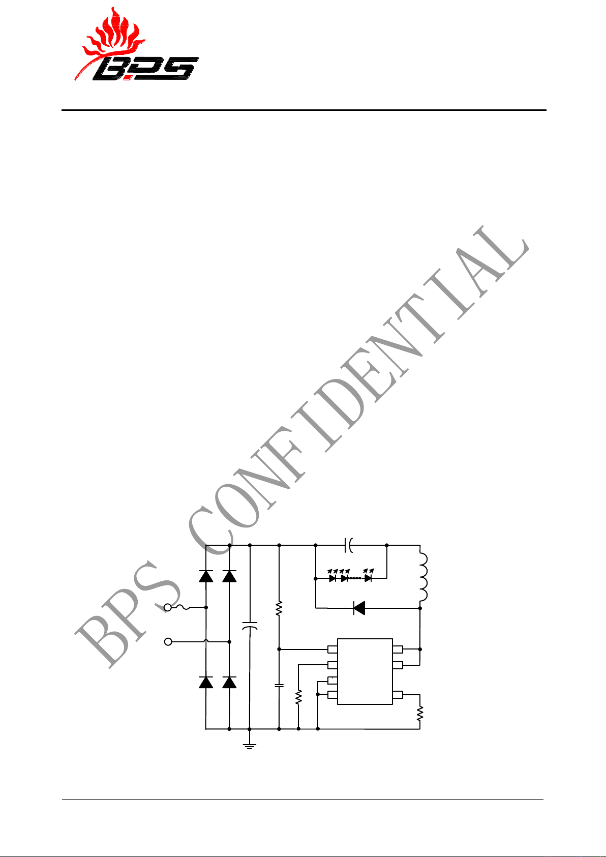
Typical Application
BP2865E
AC
NC
GND CS
DRAIN
7
6
5
1
2
4
VCC
ROVP DRAIN
3
Figure 1. Typical application circuit for BP2865E
Page 2
BP2865E
Non-isolated Buck Offline LED Driver
BP2865E_EN _DS_Rev.1.0 www.bpsemi.com 2
BPS Confidential – Customer Use Only
晶丰明源半导体
Ordering Information
Part Number
Package
Operating
Temperature
Packing Method
Marking
BP2865E
DIP7
-40 ℃ to 105 ℃
Tube
50 Pcs/Tube
BP2865E
XXXXXY
WXYY
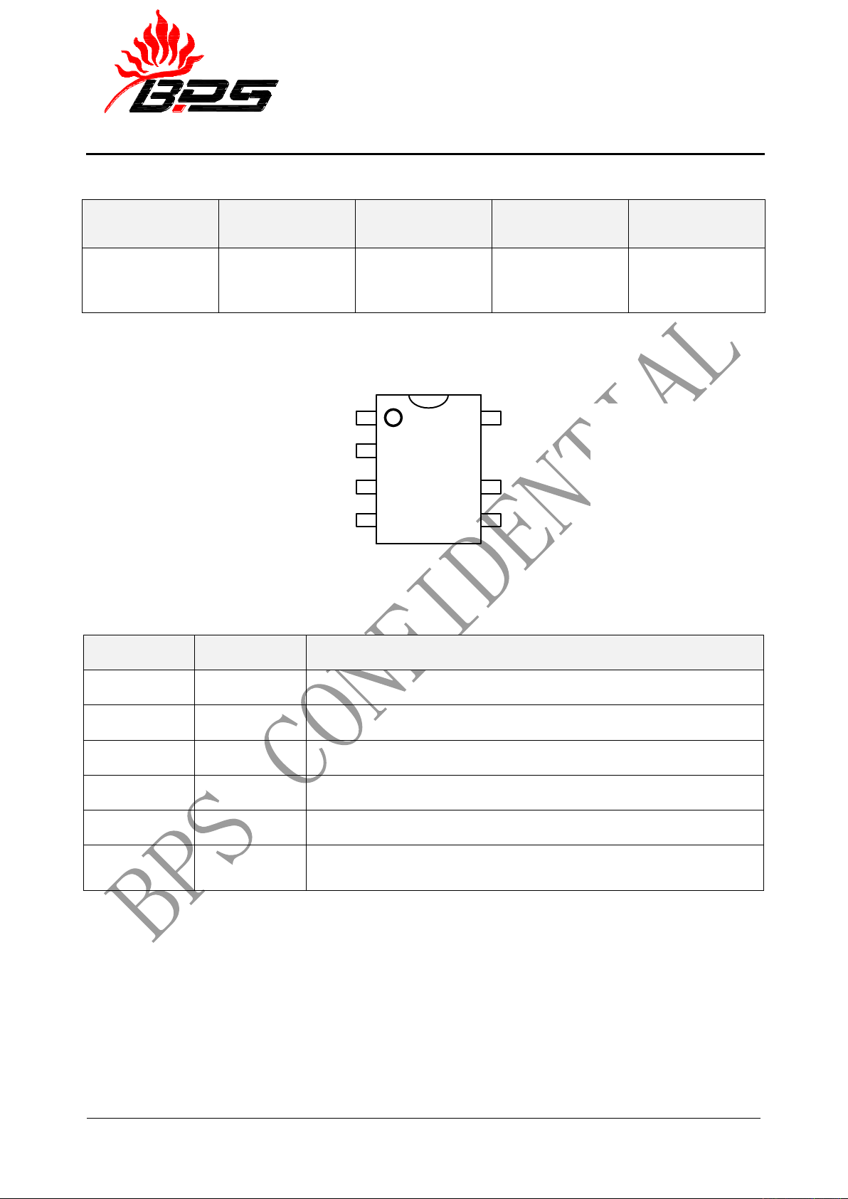
Pin Configuration and Marking Information
DRAIN
GND
DRAIN
CS
ROVP
NC
VCC
BP2865E
XXXXXY
WWXYY
Figure 2. Pin configuration
Pin Definition
Pin No.
Name
Description
1
GND
Ground 2 ROVP
Over Voltage Protection Setting Pin. Connect a resistor to GND
3
NC
No Connection. Should be connected to GND(Pin1)
4
VCC
Power Supply Pin
5,6
DRAIN
Internal HV Power MOSFET Drain.
7
CS
Current Sense Pin. Connect a sense resistor between this pin and GND
pin.
XXXXXY: Lot Code
W: Sign
X: Year
YY: Week
Page 3
BP2865E
Non-isolated Buck Offline LED Driver
BP2865E_EN _DS_Rev.1.0 www.bpsemi.com 3
BPS Confidential – Customer Use Only
晶丰明源半导体
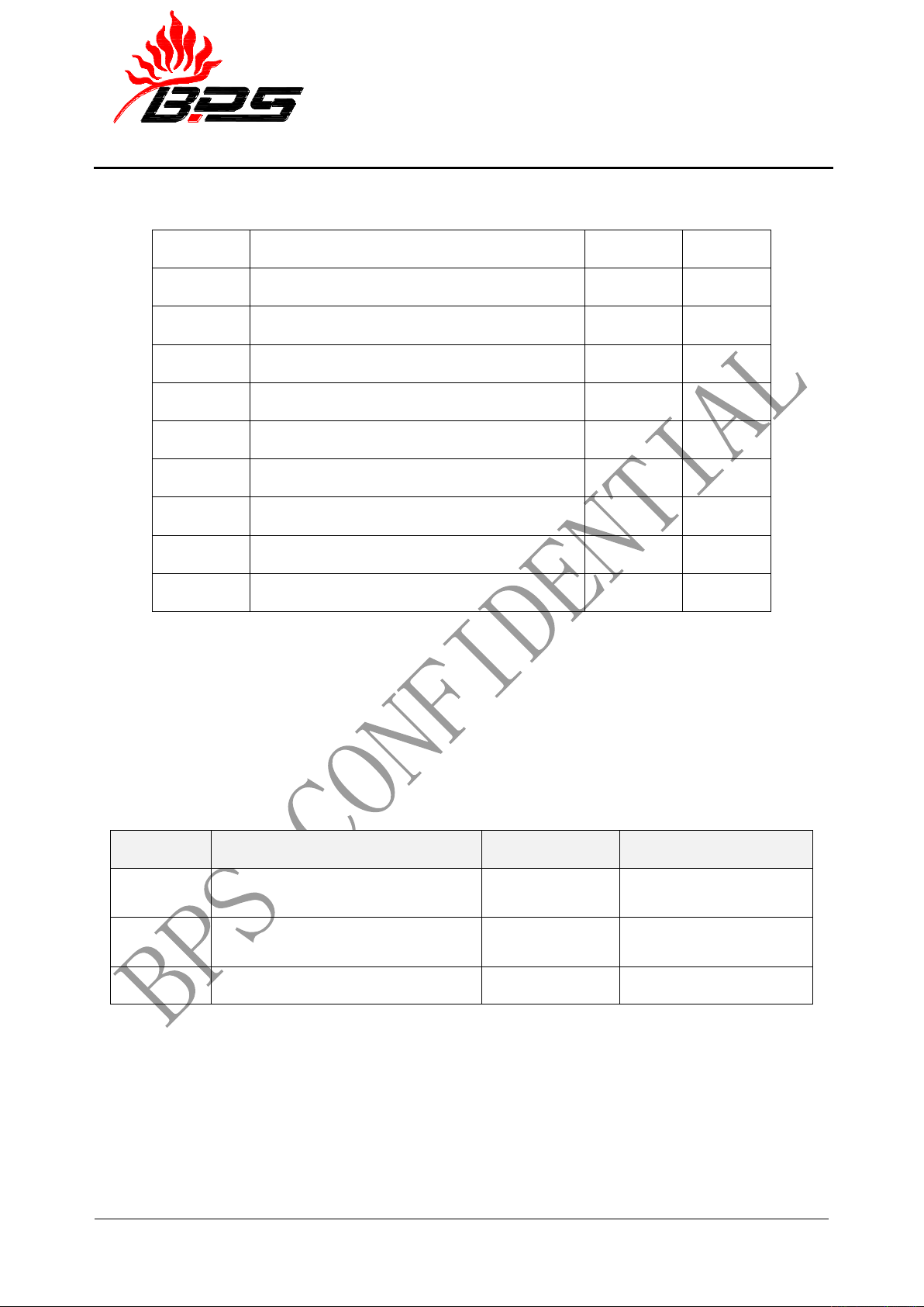
Absolute Maximum Ratings (note1)
Symbol
Parameters
Range
Units
I
CC_MAX
VCC pin maximum sink current
5
mA
DRAIN
Internal HV MOSFET drain voltage
-0.3~500
V
CS
Current sense pin input voltage
-0.3~6
V
ROVP
Over-voltage setting pin voltage
-0.3~6
V
P
DMAX
Power dissipation (note 2)
0.9
W
θ
JA
Thermal resistance (Junction to Ambient)
80
℃/W
TJ
Operating junction temperature
-40 to 150
℃
T
STG
Storage temperature range
-55 to 150
℃
ESD (note 3)
2
KV
Note 1: Stresses beyond those listed under “absolute maximum ratings” may cause permanent damage to the device. Under “recommended operating
conditions” the device operation is assured, but some particular parameter may not be achieved. The electrical characteristics table defines the operation
range of the device, the electrical characteristics is assured on DC and AC voltage by test program. For the parameters without minimum and maximum
value in the EC table, the typical value defines the operation range, the accuracy is not guaranteed by spec.
Note 2: The maximum power dissipation decrease if temperature rise, it is decided by T
JMAX
, θ
JA
, and environment temperature (TA). The maximum power
dissipation is the lower one between P
DMAX
= (T
JMAX
- T
A
)/ θ
JA
and the number listed in the maximum table.
Note 3: Human Body mode, 100pF capacitor discharge on 1.5KΩ resistor
Recommended Operation Conditions
Symbol
Parameter
Range
Unit
I
LED1
Output LED current @ Vout=72V
(Input voltage 176V~265V)
320
mA
I
LED2
Output LED current @ Vout=36V
(Input voltage 176V~265V)
360
mA
V
LED min
Minimum LED Loading Voltage
>15
V
Page 4
BP2865E
Non-isolated Buck Offline LED Driver
BP2865E_EN _DS_Rev.1.0 www.bpsemi.com 4
BPS Confidential – Customer Use Only
晶丰明源半导体
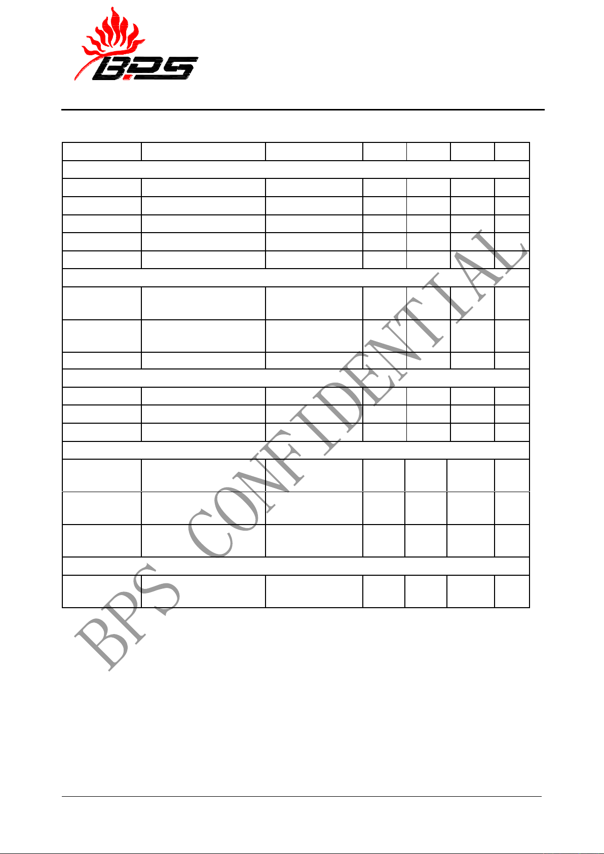
Electrical Characteristics (Notes 4, 5) (Unless otherwise specified, V
CC
=15V and TA =25 ℃)
Symbol
Parameter
Conditions
Min
Typ
Max
Units
Supply Voltage Section
V
CC_CLAMP
VCC Clamp Voltage
1mA
17 V
V
CC_ON
VCC Turn On Threshold
VCC Rising
14 V
V
CC_UVLO
VCC Turn off Threshold
VCC Falling
9 V IST
V
CC
Startup Current
VCC= V
CC-ON
- 1V
150
200
uA
IOP
V
CC
Operating Current
FOP=70KHz
180
250
uA
Current Sense Section
V
CS_TH
Threshold Voltage for
Peak Current Limit
388
400
412
mV
T
LEB
Leading Edge Blanking
Time for Current Sense
350 ns
T
DELAY
Switch Off Delay Time
200 ns
Internal Time Control Section
T
OFF_MIN
Minimum OFF Time
2
us
T
OFF_MAX
Maximum OFF Time
340 us
T
ON_MAX
Maximum On Time
40 us
MOSFET Section
R
DS_ON
Static Drain-source
On-resistance
VGS=15V/IDS=0.4A
5 Ω BV
DSS
Drain-Source Breakdown
Voltage
VGS=0V/IDS=250uA
500 V I
DSS
Power MOSFET Drain
Leakage Current
VGS=0V/VDS=500V
1
uA
Thermal Regulation Section
T
REG
Thermal Regulation
Temperature
150
℃
Note 4: production testing of the chip is performed at 25°C.
Note 5: the maximum and minimum parameters specified are guaranteed by test, the typical value are guaranteed by design, characterization and statistical
analysis
Page 5
BP2865E
Non-isolated Buck Offline LED Driver
BP2865E_EN _DS_Rev.1.0 www.bpsemi.com 5
BPS Confidential – Customer Use Only
晶丰明源半导体
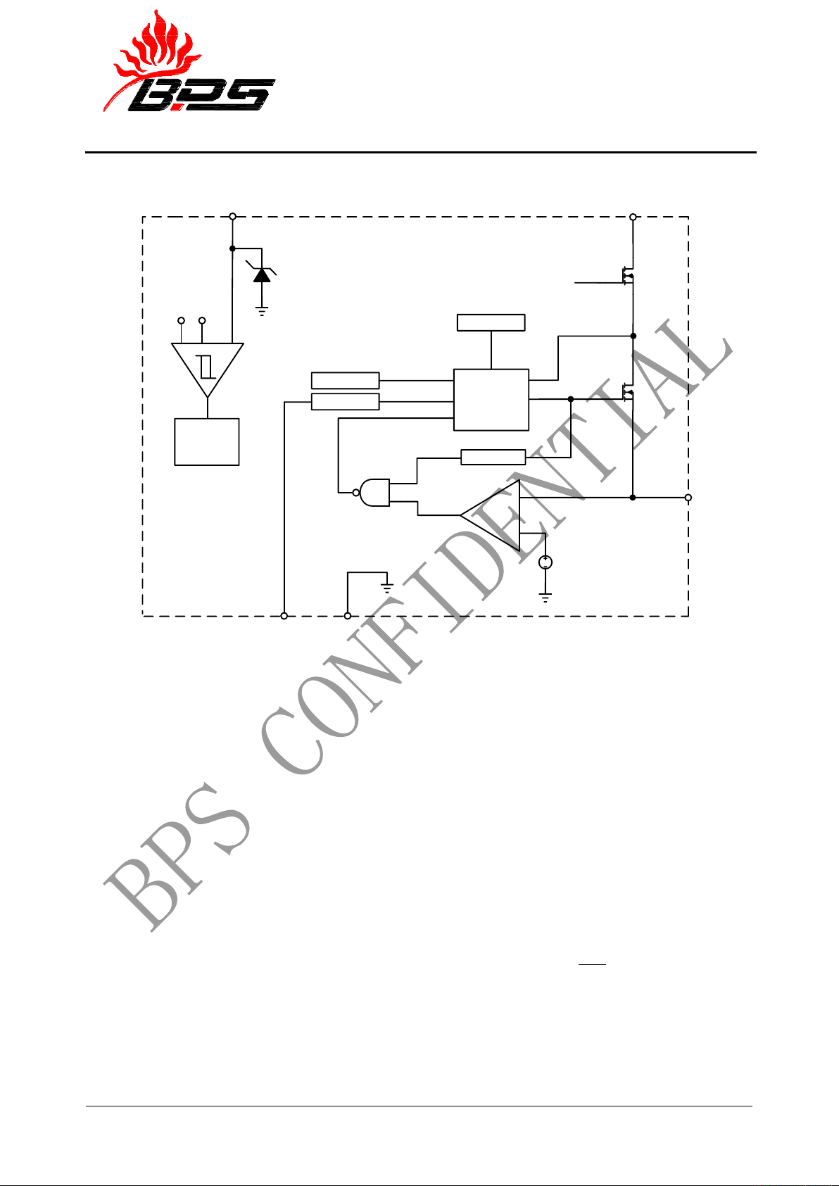
Internal Block Diagram
VCC
UVLO
+
-
-
RESET
14V
9.0V
CS
+
-
Current
Sense
GND
CC &
Logic Control
OVP
LEB
400mV
DRAIN
HV
MOSFET
OCP
OTP
VCC
ROVP
17V
Figure 3. BP2865E Internal Block Diagram
Application Information
The BP2865E is a high performance non-isolated
Buck converter specially designed for LED lighting.
The device integrates a 500V power MOSFET. With
very few external components, the converter
achieves excellent constant current control. And it
does not need auxiliary winding for powering the IC
or voltage sensing, hence the system size and cost is
greatly reduced.
Start Up
After system powered up, the VCC pin capacitor is
charged up by the start up resistor. When the VCC
pin voltage reaches the turn on threshold, the internal
circuits start operating. The BP2865E integrates a
17V zener diode to clamp the VCC voltage. Due to
the ultra-low operating current, the auxiliary winding
is not needed to supply the IC.
Constant Current Control
Cycle by Cycle current sense is adopted in BP2865E,
the CS pin is connected to the current sense
comparator, and the voltage on CS pin is compared
with the internal 400mV reference voltage. The
MOSFET will be switched off when the voltage on
CS pin reaches the threshold. The CS comparator
includes a 350ns leading edge blanking time.
The peak inductor current is given by:
)mA(
R
400
I
CS
PK
Where, R
CS
is the current sense resistor value.
The current in LED can be calculated by the
equation:
Page 6

BP2865E
Non-isolated Buck Offline LED Driver
BP2865E_EN _DS_Rev.1.0 www.bpsemi.com 6
BPS Confidential – Customer Use Only
晶丰明源半导体
2
I
I
PK
LED
Where, IPK is the peak current of the inductor.
Inductor Selection
The BP2865E works under inductor current critical
conduction mode. When the power MOFET is
switched on, the current in the inductor rises up from
zero, the on time of the MOSFET can be calculated
by the equation:
LEDIN
PK
on
VV
IL
t
Where,
L is the inductance value
VIN is the DC bus voltage after the rectifier bridge
V
LED
is the voltage on the LED
After the power MOSFET is switched off, the
current in the inductor decreases. When the inductor
current reaches zero, the power MOSFET is turned
on again by IC internal logic. The off time of the
MOSFET is given by:
LED
PK
off
V
IL
t
The inductance can be calculated by the equation:
IN
PK
LEDINLED
VIf
)VV(V
L
The f is the system switching frequency, which is
proportional to the input voltage. So the minimum
switching frequency is set at lowest input voltage,
and the maximum switching frequency is set at
highest input voltage.
The minimum and maximum off time of BP2865E is
set at 2us and 240us, respectively. Referring to the
equation of t
OFF
calculation, if the inductance is too
small, the t
OFF
may be smaller than the minimum off
time, system will operate in discontinuous
conduction mode and the output current will be
smaller than the designed value. If the inductance is
too large, the t
OFF
may be larger than the maximum
off time, the system will operate in continuous
conduction mode and the output current will be
higher than the designed value. So it is important to
choose a proper inductance.
Over Voltage Protection
The over voltage protection can be programmed by
the ROVP pin resistor. The ROVP pin current is
50uA.
When the LED is open circuit, the output voltage
increases gradually, and the demagnetization time
gets shorter. The demagnetization time at OVP---Tovp can be calculated by the open circuit protection
voltage:
VovpRcs
VcsL
Tovp
Where,
Vcs is the CS pin turn off threshold (400mV)
Vovp is the open circuit protection voltage
And then the Rovp resistor value can be calculated
by the equation:
3-
10*
ovp
031
T
Rovp
(kohm)
Protection Function
The BP2865E offers rich protection functions to
improve the system reliability, including LED
open/short protection, CS resistor short protection,
VCC under voltage protection, thermal regulation.
When the LED is open circuit, the system will
trigger the over voltage protection and stop
switching.
When the LED short circuit is detected, the system
Page 7

BP2865E
Non-isolated Buck Offline LED Driver
BP2865E_EN _DS_Rev.1.0 www.bpsemi.com 7
BPS Confidential – Customer Use Only
晶丰明源半导体
works at low frequency (5kHz), and the CS pin turn
off threshold is reduced to 200mV. So the system
power consumption is very low. At some
catastrophic fault condition, such as CS resistor
shorted or inductor saturated, the internal fast fault
detection circuit will be triggered, the system stops
switching immediately.
After the system enters into fault condition, the VCC
voltage will decrease until it reaches the UVLO
threshold, then the system will re-start again. If the
fault condition is removed, the system will recover to
normal operation.
Thermal Regulation
The BP2865E integrates thermal regulation function.
When the system is over temperature, the output
current is gradually reduced; the output power and
thermal dissipation are also reduced. The system
temperature is regulated and the system reliability is
improved. The thermal regulation temperature is set
to 150℃ internally.
PCB Layout
The following rules should be followed in BP2865E
PCB layout:
Bypass Capacitor
The bypass capacitor on VCC pin should be as close
as possible to the VCC Pin and GND pin.
ROVP Pin
The ROVP resistor should be as close as possible to
the ROVP Pin.
Ground Path
The power ground path for current sense should be
short, and the power ground path should be separated
from small signal ground path before connecting to
the negative node of the bulk capacitor.
The Area of Power Loop
The area of main current loop should be as small as
possible to reduce EMI radiation, such as the
inductor, the power MOSFET, the output diode and
the bus capacitor loop.
NC pin
The NC pin should be connected to GND (pin1).
Drain Pin
To increase the copper area of DRAIN pin for better
thermal dissipation. However too large copper area
may compromise EMI performance.
Page 8
BP2865E
Non-isolated Buck Offline LED Driver
BP2865E_EN _DS_Rev.1.0 www.bpsemi.com 8
BPS Confidential – Customer Use Only
晶丰明源半导体
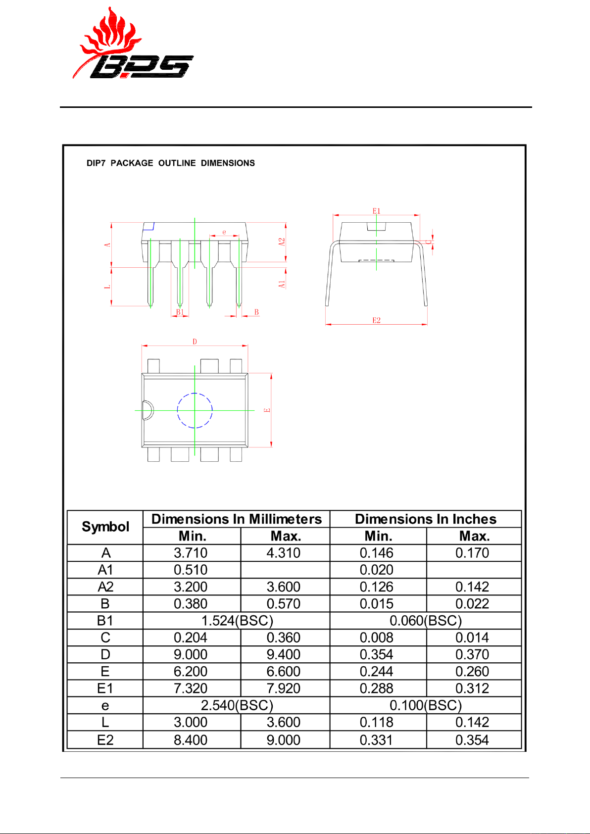
Physical Dimensions
 Loading...