

Page 1
SERVICE MANUAL
ORIGINAL VERSION
REFERENCE NO.SM5110337
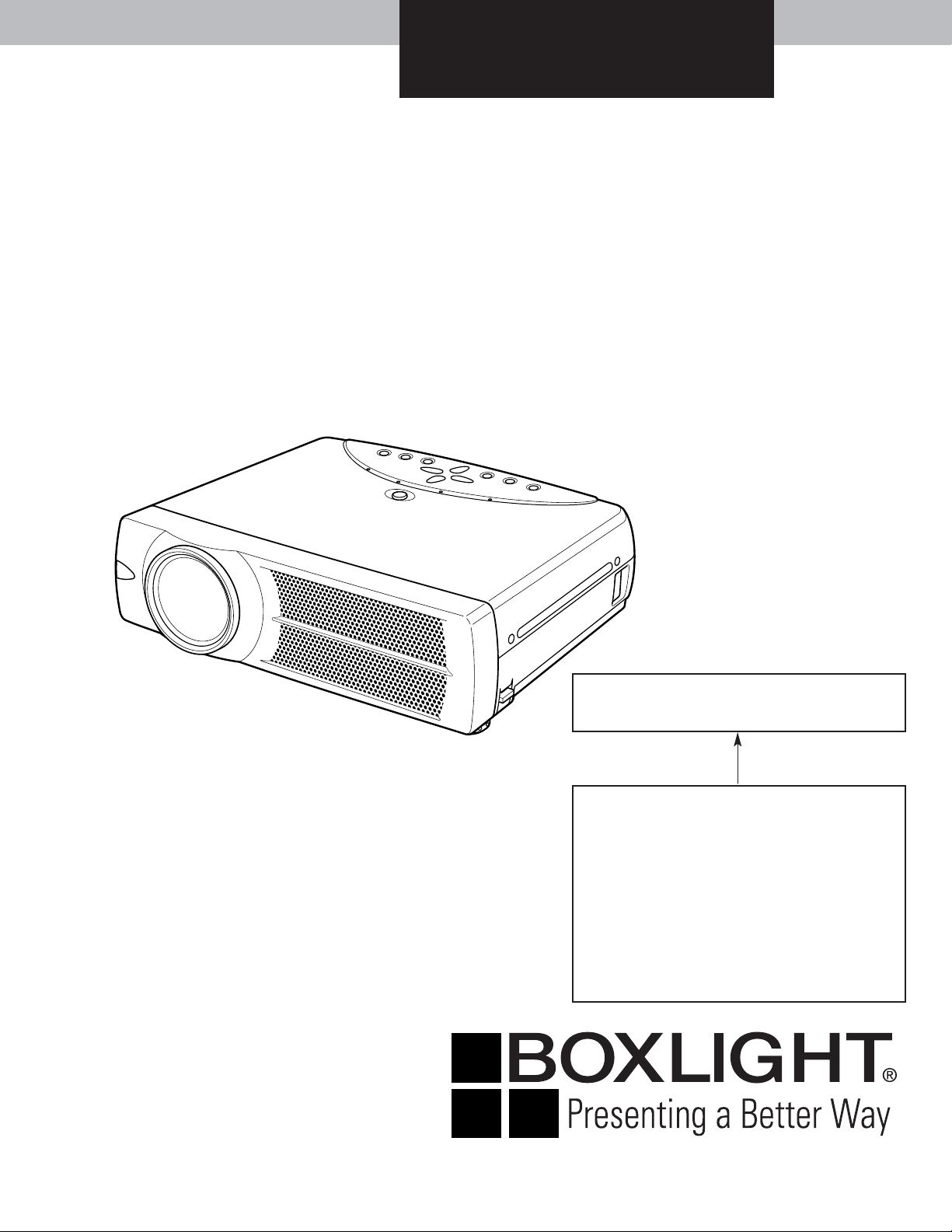
BOXLIGHT CP-305t
SERVICE MANUAL
Chassis No. MD8-CP-305t00
NOTE: Match the Chassis No. on the unit’s
back cover with the Chassis No. in the
Service Manual.
If the Original Version Service
Manual Chassis No.does not match
the unit’s, additional Service
Literature is required.You must refer to
“Notices” to the Original Service
Manual prior to servicing the unit.
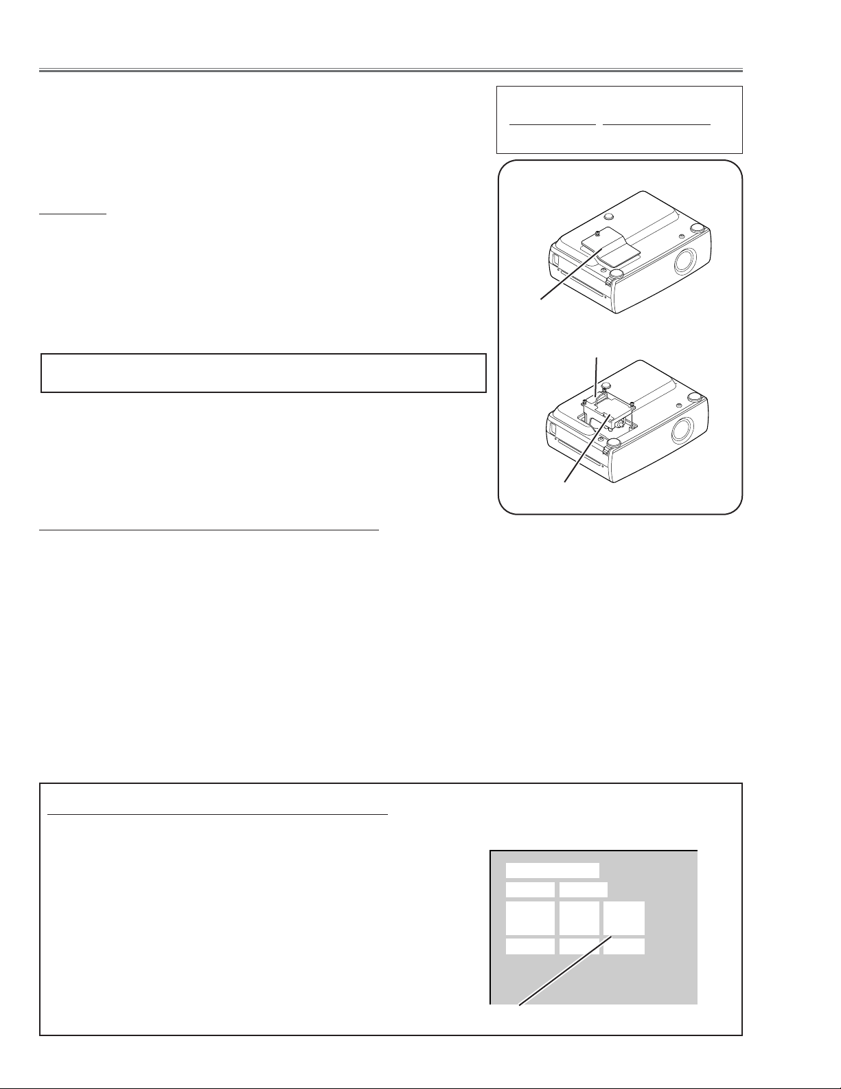
PRODUCT CODE
(MD8E) 1 122 121 04
Page 2

2
■ Contents
■ Safety instructions ________________________________________________3
■ Specifications __________________________________________________ 4
■ Note on Servicing ______________________________________________ 5
■ Adjustments after parts replacement ________________________________ 5
■ Circuit protections ______________________________________________ 6-7
● Fuse ____________________________________________________ 6
● Thermal switch ____________________________________________ 6
● Interlock switch ____________________________________________ 6
● Warning temperature and power failure protection ________________ 7
■ Mechanical disassemblies ______________________________________ 8-13
■ Optical parts disassemblies ____________________________________ 14-17
■ LCD panel/prism ass’y replacement ________________________________ 19
■ Lamp replacement ______________________________________________ 20
■ Optical adjustments __________________________________________ 21-24
● Contrast adjustment ________________________________________ 21
● Condenser lens adjustment __________________________________ 22
● Condenser lens-Out adjustment ______________________________ 23
● Relay lens-Out adjustment __________________________________ 24
■ Electric adjustments __________________________________________ 25-30
● Service adjustment menu operation____________________________ 23
● Circuit adjustments ______________________________________ 24-29
● Service adjustment data table______________________________ 30-33
● Test points and locations ____________________________________ 34
■ Troubleshooting ______________________________________________ 35-39
● No power______________________________________________ 35-36
● No picture ____________________________________________ 37-38
● No sound ________________________________________________ 39
● Lens motor problems ______________________________________ 39
■ Control port functions ________________________________________ 40-43
■ Waveforms__________________________________________________ 44-45
■ Cleaning ______________________________________________________ 46
■ IC block diagrams ____________________________________________ 47-53
■ Service parts lists ____________________________________________ 54-83
● Electrical parts list ______________________________________ 54-76
● Mechanical parts list ____________________________________ 77-78
● Optical parts list ________________________________________ 79-83
Drawings & Diagrams ______________________________________ A1-A15
■ Parts description and reading in schematic diagram____________________ A2
■ Circuit block diagram ____________________________________________ A3
■ Power supply lines ______________________________________________ A4
■ Schematic diagrams ________________________________________ A5-A11
■ Printed wiring board diagrams ________________________________ A12-A14
■ Pins description of ICs, transistors, diodes __________________________ A15
Page 3
3
■ Safety Instructions
WARNING:
The chassis of this projector is isolated (COLD) from AC line by using the converter transformer.Primary side of
the converter and lamp power supply unit circuit is connected to the AC line and it is hot, which hot circuit is identified with the line ( ) in the schematic diagram. For continued product safety and protection of personnel
injury, servicing should be made with qualified personnel.
The following precautions must be observed.
SAFETY PRECAUTIONS
1: An isolation transformer should be connected in the
power line between the projector and the AC line
before any service is performed on the projector.
2: Comply with all caution and safety-related notes pro-
vided on the cabinet back, cabinet bottom, inside the
cabinet or on the chassis.
3: When replacing a chassis in the cabinet, always be
certain that all the protective devices are installed
properly, such as, control knobs, adjustment covers
or shields, barriers, etc.
DO NOT OPERATE THIS PROJECTOR WITHOUT
THE PROTECTIVE SHIELD IN POSITION AND
PROPERLY SECURED.
4: Before replacing the cabinet cover, thoroughly
inspect the inside of the cabinet to see that no stray
parts or tools have been left inside.
Before returning any projector to the customer, the
service personnel must be sure it is completely safe to
operate without danger of electric shock.
SERVICE PERSONNEL WARNING
Eye damage may result from directly viewing the light produced by the Lamp used in this equipment. Always turn
off Lamp before opening cover.The Ultraviolet radiation eye protection required during this servicing.
Never turn the power on without the lamp to avoid electric-shock or damage of the devices since the stabilizer
generates high voltages(15kV - 25kV) at its starts.
Since the lamp is very high temperature during units operation replacement of the lamp should be done at least
45 minutes after the power has been turned off, to allow the lamp cool-off.
PRODUCT SAFETY NOTICE
Product safety should be considered when a component replacement is made in any area of the projector.
Components indicated by mark in the parts list and the schematic diagram designate components in which
safety can be of special significance.It is, therefore, particularly recommended that the replacement of there parts
must be made by exactly the same parts.
DO NOT ATTEMPT TO SER VICING THE
REMOTE CONTROL UNIT.
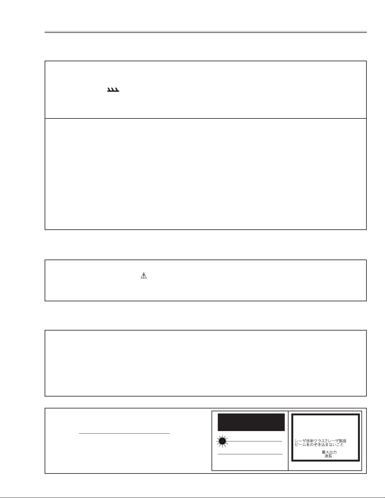
Laser Beam may be leaked out when in disassemble
the Unit. As the Laser Beam used in this Remote control unit is harmful to the eyes.
LASER RADIATION
DO NOT STARE INTO BEAM
MAX. OUTPUT: 1mW
WAVE LENGTH: 650±20nm
CLASS
II LASER PRODUCT
This product is complied with 21 CFR
part 1040.10
CAUTION
LASER RADIATION
DO NOT STARE INTO BEAM
CLASS 2 LASER PRODUCT
LASER-STRAHLING
NICHT IN DEN STRAHL BLICKEN
LASER KLASSE 2
IEC60825-1, Am. 1 1997
MAX OUTPUT ( ) : 1 mW
WAVE LENGTH ( ) : 650±20nm
Page 4

Projector Type Multi-media Projector
Dimensions (W x H x D) 13.11” x 3.52” x 9.96” (333mm x 89.5mm x 253mm)
Net Weight 9.5 lbs (4.3 kg)
LCD Panel System 0.9” TFT Active Matrix type, 3 panels
Panel Resolution 1024 x 768 dots
Number of Pixels 2,359,296 (1024 x 768 x 3 panels)
Color System 6 color system (PAL, SECAM, NTSC, NTSC4.43, PAL-M and PAL-N)
High Definition TV SIgnals 480i, 480p, 575i, 575p, 720p. 1035i and 1080i
Scanning Frequency H-sync. 15 ~ 100kHz, V-sync. 50 ~ 100Hz
Projection Image Size (diagonal) Adjustable from 34” to 300”
Horizontal Resolution 800 TV lines
Projection Lens F 1.9 ~ 2.1 lens with f 21.3mm ~ 25.6mm with motor zoom and focus
Throw Distance 3.0’~ 22.6’(0.9m ~ 6.9m)
Projection Lamp 200watts
AV Input Jacks RCA Type x 3 (Video/Y, Cb/Pb, Cr/Pr) and Mini DIN 4 pin x 1(S-Video)
AV Audio Input Jacks RCA Type x 2
Computer Input Jacks (VGA) HDB15 Ter minal x 1
Monitor Output Jacks (VGA) HDB15 Terminal x 1
Computer Audio Input Jack Mini Jack (stereo)
Control Port Connector Mini DIN 8 pin x 1
USB Connector USB Series B receptance x 1
External Speaker Jack Mini Jack (8Ω 1+1W / stereo)
Internal Audio Amp. 1.0watt RMS (monaural)
Built-in Speaker 1 speaker, 1.18” x 1.57” (30mm x 40mm)
Feet Adjustment 0˚ to 15.6˚
Voltage and AC 100 ~ 120V (3.6A Max. Ampere), 50/60Hz (The U.S.A and Canada)
Power Consumption AC 200 ~ 240V (1.8A Max. Ampere), 50/60Hz (Continental Europe )
Operating Temperature 41˚F ~ 95˚F (5˚C ~ 35˚C)
Storage Temperature 14˚F ~ 140˚F (-10˚C ~ 60˚C)
Remote Control Transmitters Wireless Remote Control, batteries AA, UM3 or R06 Type x 2
4
■ Specifications
● The specifications are subject to change without notice.
This symbol on the nameplate means the product is Listed by Underwriters
Laboratories Inc. It is designed and manufactured to meet rigid U.L. safety standards against risk of fire, casualty and electrical hazards.
Page 5
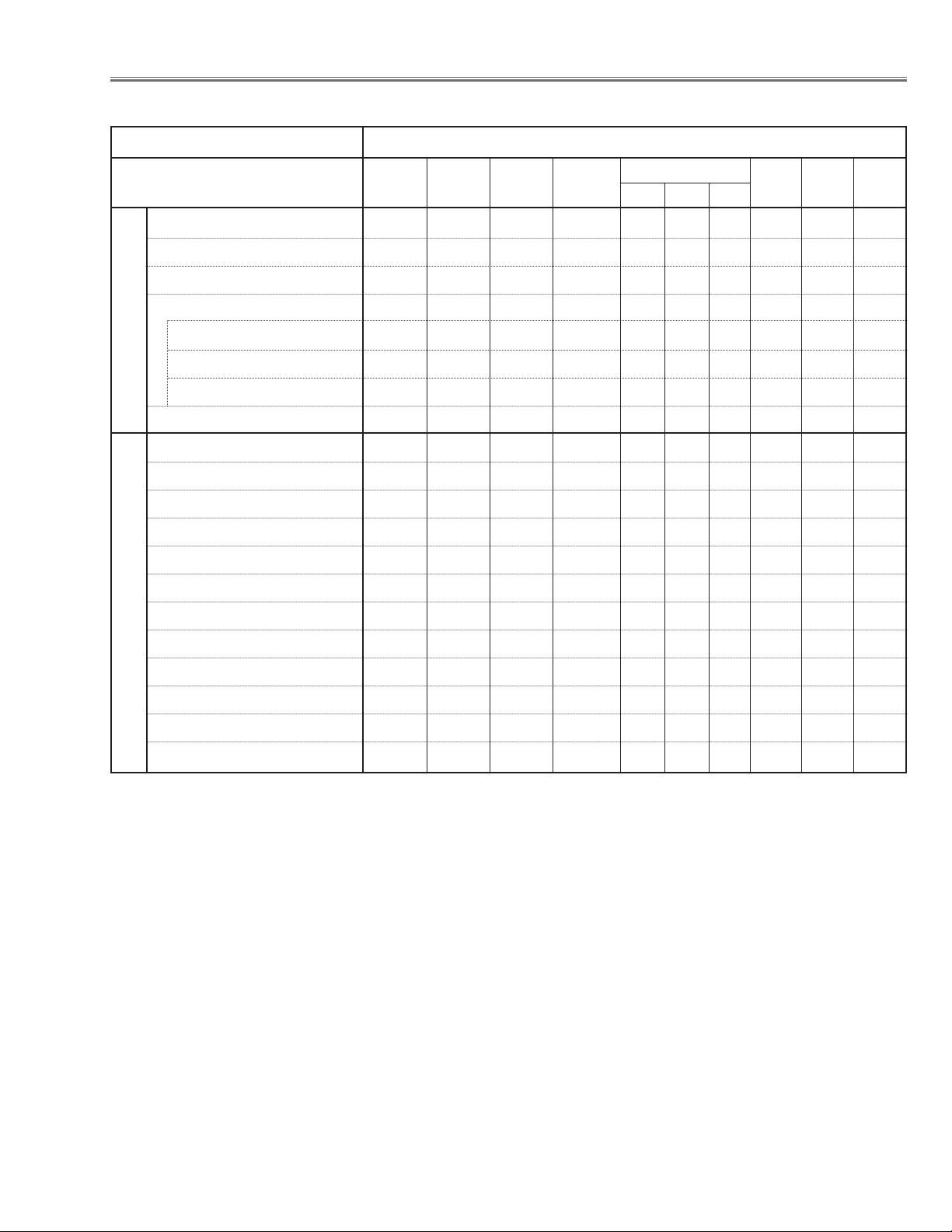
5
Condenser lens adjustment ❍●
Condenser lens-out adjustment ❍●
Relay lens-out adjustment ❍●
Contrast Adjustment
R-Contrast adjustment ●
G-Contrast adjustment ●
B-Contrast adjustment ●
Output voltage adjustment ●
Fan voltage adjustment ●
Pedestal adjustment ●
NRS adjustment ●
Signal center adjustment ●
Black level adjustment ●
PC offset adjustment ●
PC gain adjustment ●
AV gain adjustment ●
Common center adjustment ● ●
Gamma shift adjustment ❍ ●
White balance adjustment ❍ ❍
Disassembly / Replaced Parts
LCD/
Prism
Ass’y
Condenser
Lens
Polarized glass
RGB
Optical Adjustments
Electrical Adjustments
● : Adjustment necessar y ❍ : Check necessary
P. F.
Board
Main
Board
Condenser
Lens-Out
■ Adjustments after Parts Replacement
Relay
Lens-Out
Power
Board
Page 6
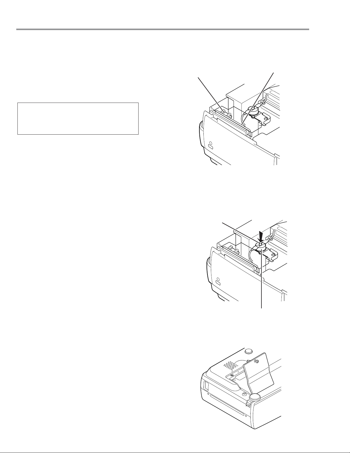
-6-
● Interlock switch
The interlock switch (SW904) cuts off the AC mains power supply
when the lamp cover is removed. After opening the lamp cover for
replacing the lamp ass’y, place the lamp cover correctly otherwise
the projector can not turn on.
● Thermal switch
There is the thermal switch (SW902) inside of the projector to
prevent the internal temperature from rising abnormally.When the
internal temperature reaches near 100˚C, turn off the AC main
power supply automatically.
The thermal switch is not reset to normal automatically even if the
internal temperature becomes normal. Reset the thermal switch
following procedure.
Check the resistance between terminals of thermal switch by
using the tester.If it has high impedance, thermal switch may be
in operative.
How to reset the thermal switch
1.
Remove the cabinet top following to “Mechanical
Disassemblies”.
2. Press the reset button on the thermal switch.
CAUTION:
Before press the reset button, disconnect the AC cord from the
projector.
■ Circuit Protections
This projector is equipped with the following circuit protections to operate in safety. If the abnor mality occurs inside
the projector, it will automatically turn off by operating one of the following protection circuits.
● Fuse
The fuse is located inside of the projector.When either the LAMP
indicator or the READY indicator is not illuminated, fuse may be
opened. Check the fuse as following steps.
It should be used the specified fuse as follows;
How to replace the fuse
1. Remove the cabinet top following to “Mechanical
Disassemblies”.
2. Remove the fuse from fuse holder.
To install the fuse, take reversed step in the above.
Fuse Part No.: 423 022 2102
TYPE T4.0AH 250V FUSE
LITTLE FUSE INC.TYPE 215004
Fuse
Thermal switch (SW902)
Reset Button
Line Filter Board
Page 7
-7-
Circuit Protections
● Warning temperature and power failure protection
The TEMP WARNING indicator flashes red and the projector will automatically turn off when the internal temperature of the projector exceeds the normal temperature or when stopping cooling fans or when the internal power
supply lines are failed.
Check the following possible causes and wait until stopping the TEMP WARNING indicator flashing.
Possible causes
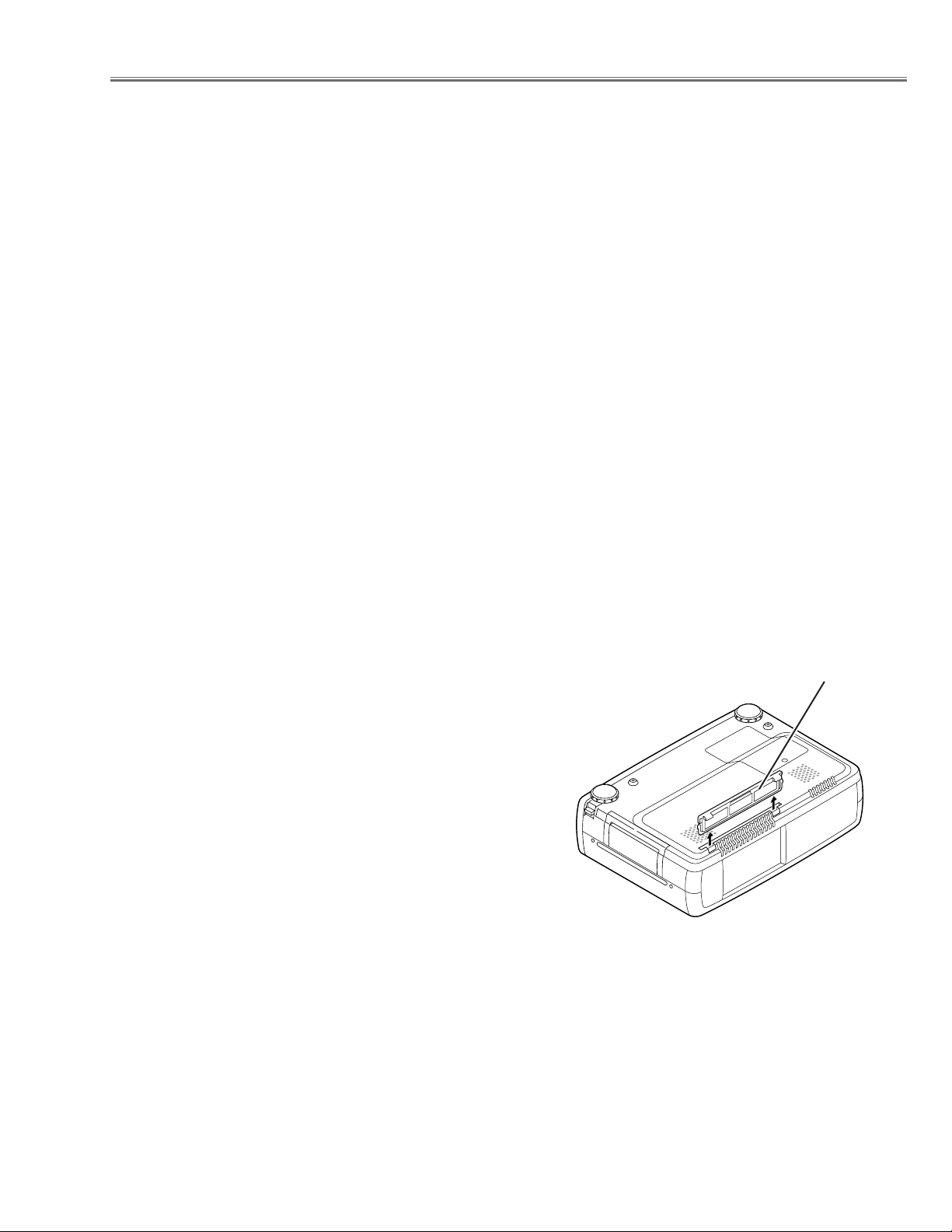
- Air filter is clogged with dust particles. Remove dust from the air filter by following instructions in the “Air filter
care and cleaning” below.
- Ventilation slots of the projector are blocked. In such an event, reposition the projector so that ventilation slots are
not obstructed.
- Check if projector is used at higher temperature place (Normal operating temperature is 5 to 35 ˚C or 41 to 95˚F)
If the TEMP WARNING indicator still continues to flash, there may be defects on cooling fans or power supply circuits. Please check fan operation and power supply lines referring to the “Power Supply Lines Chart”.
Air filter care and cleaning
The removable air filter prevents dust from accumulation on the surface of the projection lens and projection mirror.
Should the air filter become clogged with dust particles, it will reduce the cooling fan’s effectiveness and may result
in internal heat build up and reduce the life of the projector.
To clean up the air filter, follow the cleaning procedure
below:
1. Turn the power off, and disconnect the AC power cord
from the AC outlet.
2. Turn the projector up side down and remove an air filter
by pulling the latches of them upward.
3. Clean the air filter with brush or wash out the dust and
particles.
4. Replace the air filter properly. Make sure that the air fil-
ter is fully inserted.
CAUTION:
Do not operate the projector with the air filter removed.The
dust is stuck on the LCD panel and the mirror, and it may
spoil the fine picture image.
Do not put the small parts into the air intake vents. It may
result in the malfunction of the projector.The air filter is
small parts. Take care that children don’t eat or swallow it.
RECOMMENDATION
We recommend to avoid dusty, smoky place for operating the projector.Using in dusty place may cause the picture
of poor quality.
When using under the dusty or smoky conditions, dust may accumulate on the LCD panel and lens inside it, and
may resultantly be projected on the screen together with the picture.
When the above symptoms are noticed, please clean up the LCD panel and lens following to the “Cleaning
Method”.
Air filter
Page 8
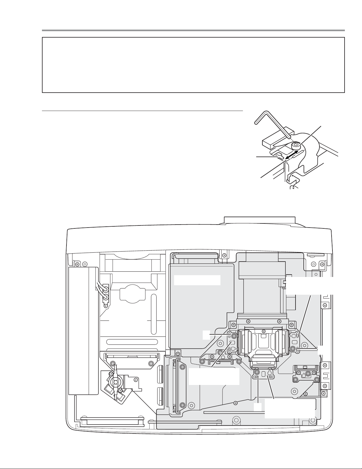
-8-
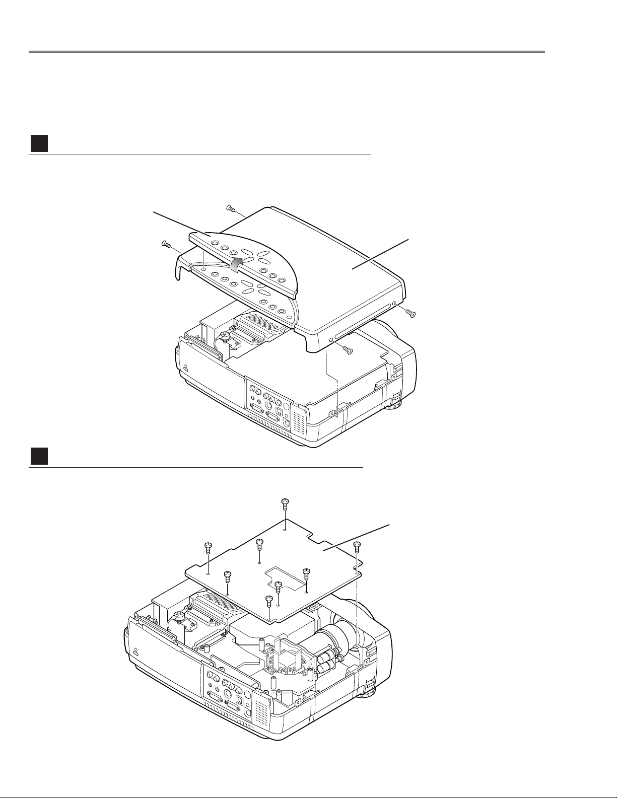
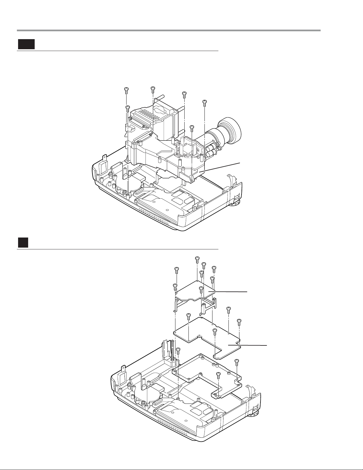
1 Remove 4 screws A to take the Cabinet Top Ass’y upward off.
2 Remove the Control Panel off from the Cabinet Top by lifting the edge of
control panel.
■ Mechanical Disassemblies
Mechanical disassemble should be made following procedures in numerical order.
Following steps show the basic procedures, therefore unnecessary step may be ignored.
Caution:
The parts and screws should be placed exactly the same position as the original otherwise it may cause loss of
performance and product safety.
Fig.1
1 Remove 8 screws to take the Main Board upward off.
Fig.2
Cabinet Top and Control Panel removal
1
Main Board removal
2
A
A
A
A
Main Board
Control panel
Cabinet top
Page 9
Temp board
-9-
Mechanical Disassemblies
1 Remove 1 screw A to release a grounding wire.
2 Pull the Rear Panel ass’y upward.
3 Remove 4 screws B and remove the AV Board.
4 Remove 4 screws C and remove the AV Sub Board.
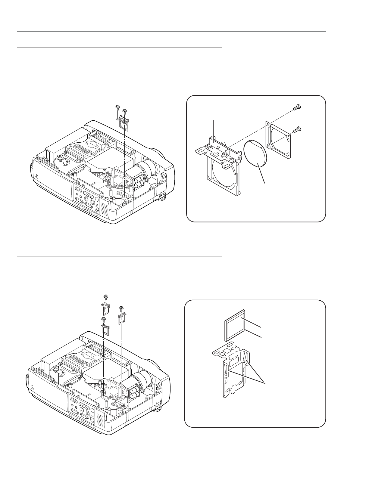
5 Remove 4 screws D and remove the speaker.
6 Remove 1 screw E and remove the Temp Board.
Fig.3
Fig.4
1 Remove 4 screws A and unhook 2 hooks B at the both of left and right
side, and the take the Front Panel ass’y off.
2 Remove 1 screw C to take the R/C Board off.
AV , AV Sub, Temp Board and Speaker removal
3
Front Panel and R/C Board removal
4
A
B
B
B
C
A
A
A
A
B
C
AV Sub board
AV board
Speaker
R/C board
B
C
C
D
D
E
Page 10
-10-
Mechanical Disassemblies
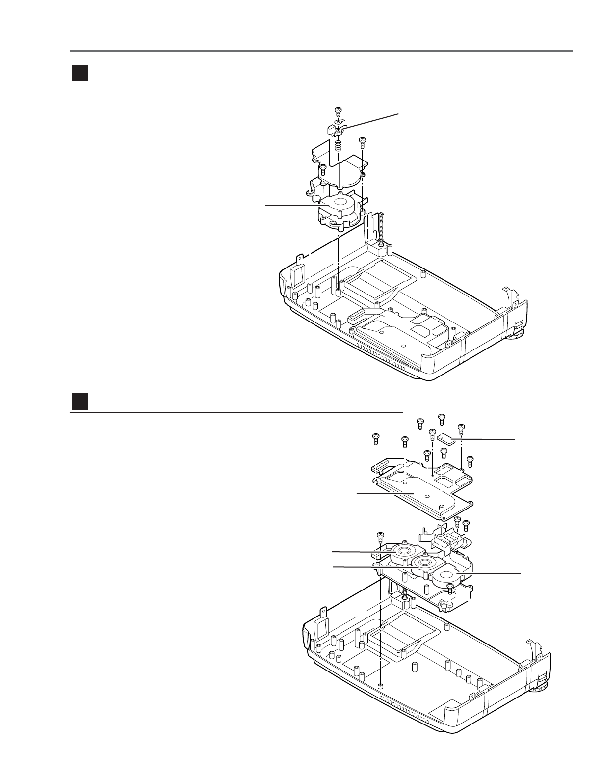
1 Remove 1 screw A and disconnect the Lamp Socket.
2 Remove 2 screws B to take the Lamp Ballast ass’y upward off.
3 Remove 2 screws C to take the isolation sheet off.
4 Remove 4 screws D to take the lamp ballast board off.
Fig.5
1
Remove 3 screws A and pull the Filter Board ass’y upward.
2 Remove 1 screw B to take the grounding lead from the cabinet bottom.
3 Remove 4 screws C to take the Filter Board off.
Fig.6
Lamp Ballast Unit removal
5
Filter Board removal
6
A
Lamp ballast board
B
B
D
D
D
D
A
A
A
B
C
C
C
C
Filter board
C
C
Isolation sheet
Page 11

-11-
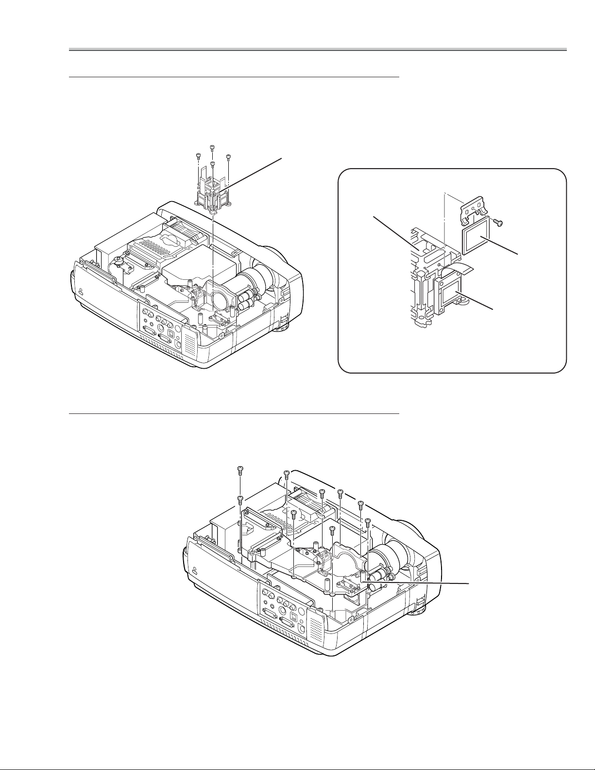
1 Remove 4 screws A to take the Fan(FN901) off.
2 Remove 4 screws B to take the Fan(FN905) off.
3 Remove 3 screws C to take the Power Box Cover upward off.
Mechanical Disassemblies
1 Remove 1 screw A to take the Lamp Cover off.
2 Loosen 3 screws B to take the Lamp assembly by
pulling the handle.
Step to next procedure.
Fig.8-1
Fig.7
Power Box Cover and Fans(FN901, FN906) removal
7
Optical Unit removal
8
-1
A
A
A
A
B
BB
B
C
C
C
FN901
FN906
Power box cover
Lamp cover
Lamp ass’y
A
B
B
B
Page 12
Step from previous procedure.
3 Remove 6 screws C to take the Optical Unit upward upward off.
To mount optical unit, mount optical unit first then mount the Lamp assembly
and Lamp Cover.
-12-
Mechanical Disassemblies
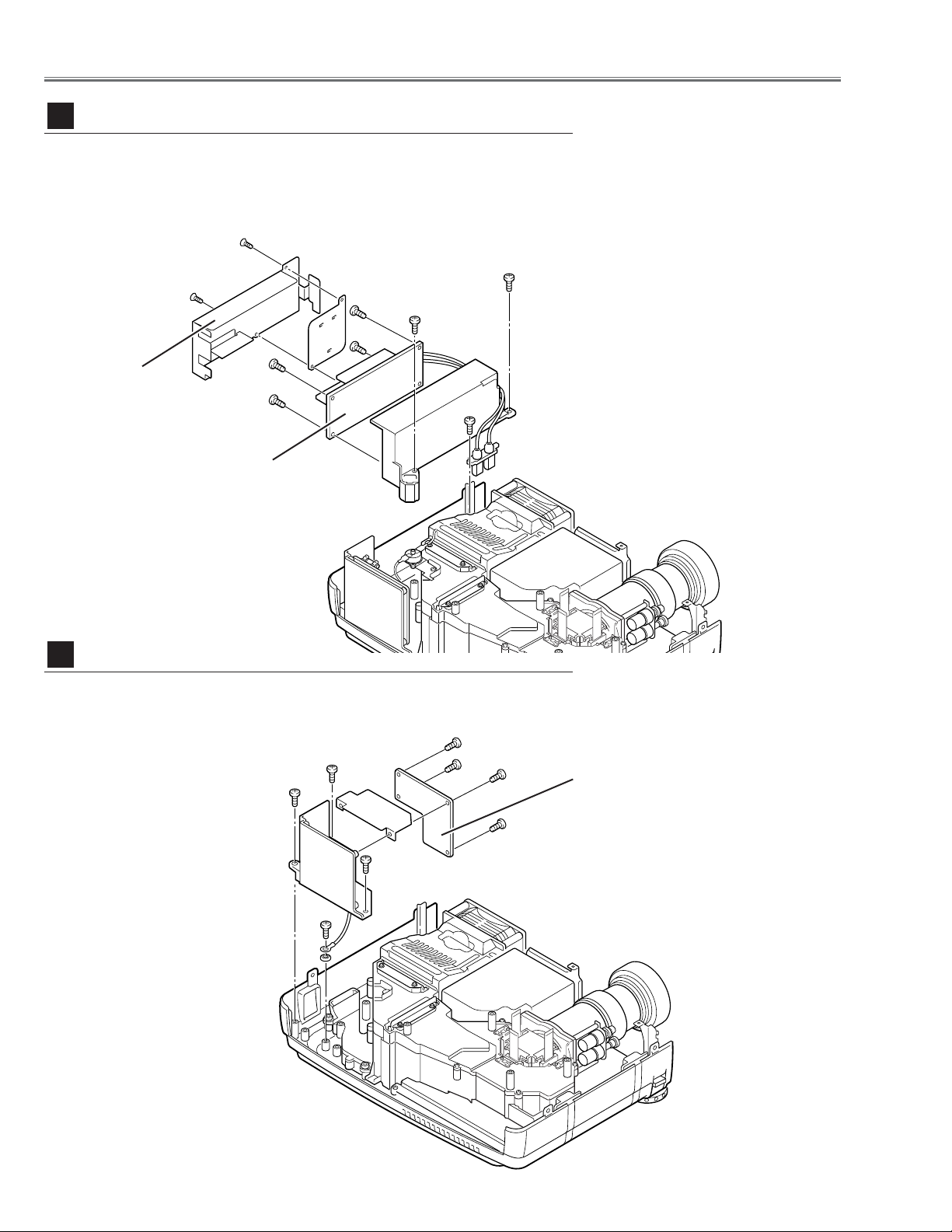
1 Remove 8 screws A to take the Power Board ass’y
upward off.
2 Remove 4 screws B to take the P.F. Board from the
Power Board.
3 Remove 3 screws C to take the Power Board holder
from the Cabinet Bottom.
Fig.9
Power and P.F. Board removal
9
A
Power board
A
A
A
A
A
A
A
B
B
B
B
C
C
C
P. F. board
Fig.8-2
Optical Unit removal
8
-2
Optical unit
C
C
C
C
C
C
Page 13
1 Remove 1 screw A and take a Washer, Spring and
Interlock Switch lever.
2 Pull the Fan and duct ass’y upward, then remove the
2 screws B to take the Fan (FN906) off.
-13-
Mechanical Disassemblies
Fig.10
1 Remove 1 screw A to take the Temp. Board off.
2 Remove 8 screws B and to take the Fan Duct
Top off and remove the Fans (FN902, FN903,
FN904).
3 Remov e 4 screws Cto take the F an Duct Bottom
off from the Cabinet Bottom.
Fig.11
Fan (FN905) removal
10
Temp Board and Fans (FN902, FN903, FN904) removal
11
Interlock switch lever
A
B
B
FN905
A
B
B
B
B
B
B
B
C
C
C
C
FN904
FN903
FN902
Temp board
Fan duct top
Page 14
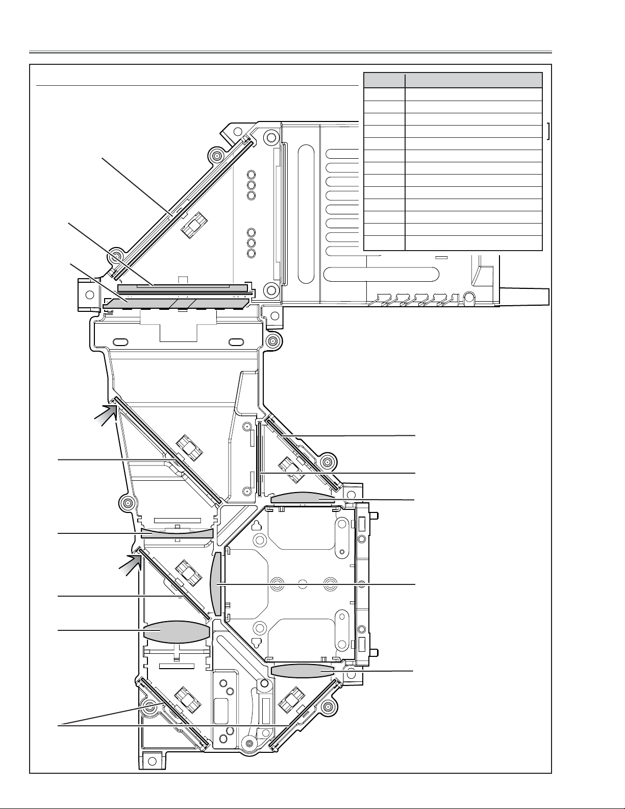
-14-
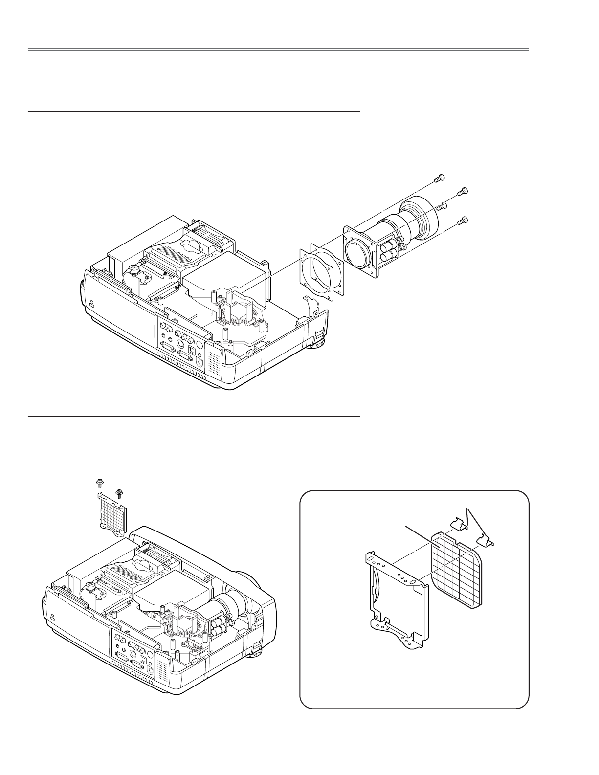
1 Remov e the Front Panel f ollowing to “Front P anel Remo v al”on “Mechanical
Disassemblies”.
2 Remove 4 screws to take the Projection Lens ass’y off.
1 Remove 2 screws A and pull the Integrator Lens-In ass’y upward.
2 Remove 1 stoppers B and then take the Lens off from the holder.
Fig.1
■ Optical Parts Disassemblies
Before taking this procedure, remove Cabinet Top and Main Board following to the “Mechanical Disassemblies”.
Disassembly requires a 2.0mm hex wrench and a screwdriver.
Integrator Lens
* Lens should be placed as the
rugged surface side comes to
the holder side.
Fig.2-
1
Fig.2-2
Projection Lens removal
Integrator Lens-In disassembly
Stopper B
A
A
Page 15
-15-
1 Remove 2 screws A and pull the Condenser Lens ass’y upward.
2 Remove 4 screws B to take the Lens off from the holder.
1 Remove 2 screws A and pull the Condenser Lens-Out ass’y upward.
2 Remove 2 screws B to take the Lens off from the holder.
Note:
Should be place the lens as shown in the figure.
A
Optical Pats Disassemblies
B
Condenser Lens
Fig.3-2
Fig.3-1
* Lens should be placed as the flat
surface side comes to the holder
side.
Holder
A
A
Fig.4-2
Fig.4-1
B
B
Holder
Condenser Lens-Out
A
Condenser lens disassembly
Condenser Lens-Out disassembly
B
B
B
Side View
Page 16
-16-
Optical Parts Disassemblies
1 Remove 2 screws A and pull the Relay Lens-Out ass’y upward.
2 Remove 2 screws B to take the Lens off from the holder.
Note:
There is no mounting direction of the lens.
1 Remove each screw and pull the Polarized Glass-In ass’y upward.
2 Unhook the stoppers and take the glass off upward.
Hooks
Polarized Glass-In
Fig.6-2
Fig.6-1
* Should be places the glass as the
film attached side comes to the
prism side.
Phase Sheet
A
Fig.5-2
Fig.5-1
B
B
Holder
Relay Lens-Out
A
Relay Lens-Out disassembly
Polarized Glass-In removal
Page 17
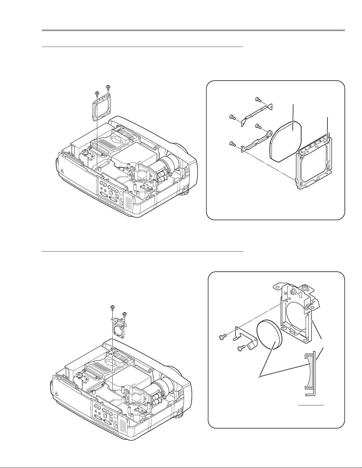
-17-
1 Remove 4 screws A and take the LCD/Prism ass’y off upward from the
optical unit.
2 Remove each screw B and take the glass off upward.
Polarized
Glass-Out
LCD Panel/Prism
Ass’y
LCD Panel/Prism Ass’y
Fig.7-
2
* Glass should be placed as the film
attached side comes to the LCD
panel side.
LCD Panel
Note:
Do not replace the LCD panel
separately otherwise it can
not obtain proper picture.
1 Remove 9 screws to take the Optical Unit Top off upward.
Fig.7-1
Fig.8
Polarized Glass-Out removal
Optical Unit Top removal
Optical Parts Disassemblies
B
A
A
A
Optical Unit Top
Page 18
-18-
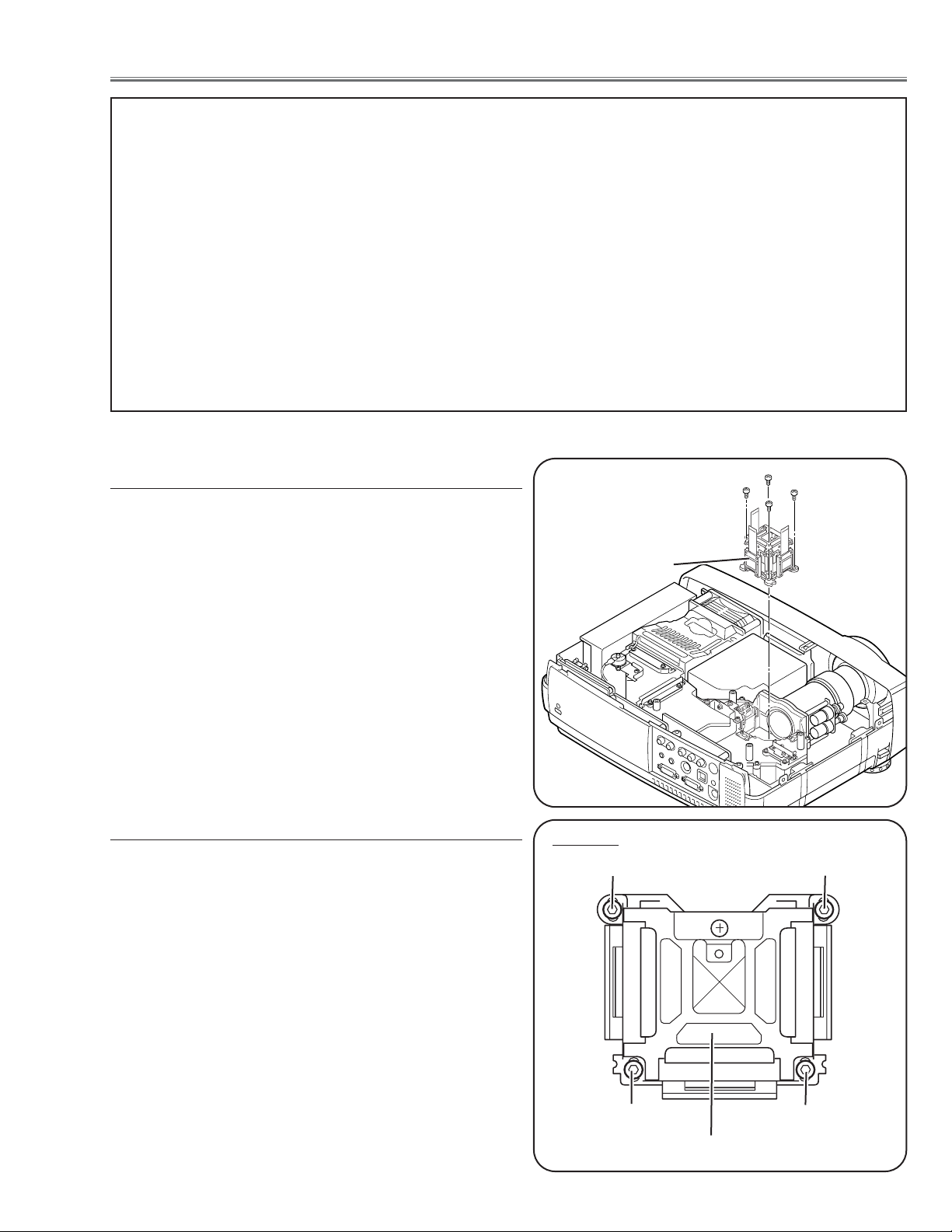
Optical Parts Disassemblies
When mounting or assembling the optical parts in the optical unit, the
parts must be mounted in the specified location and direction as
shown in figure below.
5
8
9
Fig.9
2
4
1
The printed marker
comes this side.
13
3
7
10
Locations and Directions
6
12
1 Mirror (W)
2 Integrator lens (OUT)
3Prism beam splitter (PBS)
4 Dichroic mirror (B)
5 Condenser lens (OUT)
6 Dichroic mirror (G)
7Relay lens (IN)
8 Mirror (R)
9 Condenser lens (R)
10 Condenser lens
11 Condenser lens (B)
12 Optical filter (UV cut)
13 Mirror (B)
Key No. Description
The printed marker
comes this side.
11
Page 19
-19-
■ LCD Panel/Prism Ass’y Replacement
1 Remove the cabinet top and main board following to
“Mechanical Disassemblies”.
2 Remove 4 screws by using the 2.0 mm hex driver and
take the LCD Panel/Prism ass’y off upward from the
optical unit.
LCD Panel/Prism
Ass’y
After replacing or installing the LCD Panel/Prism ass'y,
please make sure to obtain the best focus in both TELE
and WIDE zoom.If the focus adjustment is required,
please adjust the positioning of LCD Panel/Prism Ass’y by
following below procedure.
Mounting Procedure:
1 Loosen 4 screws A on the LCD Panel/Prism ass'y with
2.0 mm hex driver.
2 Turn the projector on and project the image with WIDE
zoom, and adjust the FOCUS control to obtain the best
focus.
3 Turn the ZOOM control to the TELE position.
4 Move the LCD Panel/Prism Ass’y backward or forward
(about 0mm ~ 0.8mm) to obtain the proper focus.
Confirm the focus at TELE and WIDE zoom.
5 Tighten 4 screws A to fix the LCD Panel/Prism ass'y.
T
op View
A
A
A
A
LCD Panel/Prism Ass’y
Note:
Do not replace the LCD
panel separately otherwise
it can not obtain proper picture.
IMPORTANT NOTICE on LCD Panel/Prism Ass'y Replacement
LCD panels used for this model can not be replaced separately. Do not disassemble the LCD Panel/Prism Ass’y.
These LCD panels are installed with precision at the factory.When replacing the LCD panel, should be replaced
whole of the LCD panels and prism ass’y at once.
After replacing LCD Panel/Prism ass’y, please check the following adjustments.
- Check the “Condenser Lens Adjustment” , “Condenser Lens-Out Adjustment” and “Relay Lens-Out
Adjustment” following to chapter “Optical Adjustment”.
- Check the “White Balance Adjustment” , “Common Center Adjustment” and “Gamma Shift Adjustment”
following to chapter “Electrical Adjustment”.
- Check the white uniformity on the screen.
If you find the color shading, please adjust the white uniformity by using the proper computer and
“Color Shading Correction” software supplied separately.
LCD Panel/Prism Ass’y removal
Note on LCD Panel/Prism Ass’y Mounting
Page 20
-20-
WARNING:
- For continued safety, replace with a lamp assembly of the same type.
- Allow the projector to cool for at least 45 minutes before you open the
lamp cover.The inside of the projector can become very hot.
- Do not drop the lamp module or touch the glass bulb! The glass can
shatter and cause injury.
Procedure
1 Turn off the projector and disconnect the AC cord. Allow the projector to
cool for at least 45 minutes.
2 Remove a screw with a screwdriver and remove the lamp cover.
3 Remove 2 screws and pull out the lamp assembly by grasping the han-
dle.
4 Replace the lamp assembly securely and tighten 3 screws.
5 Place the lamp cover and tighten a screw.
6 Connect the AC cord to the projector and turn on.
Note:
- Do not reset the Lamp Replace Counter, except after lamp is replaced.
- The projector can not be turned-on with lamp cover removed, because
when the lamp cover is removed, the interlock switch is also released to
switch off the mains power for safety.
7 Reset the Lamp Replace Counter, see below explanation.
■ Lamp Replacement
1 Turn the projector on, and press the MENU button
and the on-screen menu will appear.Press the POINT
LEFT/RIGHT buttons to move a red frame pointer to
SETTING menu icon.
2 Press the POINT DOWN button to move a red frame
pointer to “Lamp counter reset” and then press the
SELECT button.The message “Lamp replace counter
reset?” is displayed. Move the pointer to [Yes] and the
press the SELECT button.
3 Another confirmation dialog box appears and select
[Yes] to reset Lamp Replace Counter .
Please refer to the owners manual for further information.
Recommendation
Should the air filter become clogged with dust particles,
it will reduce the cooling fan’s effectiveness and may
result in internal heat build up and short lamp life. We
recommend cleaning the air filter after the projection
lamp is replaced.
Refer to “Air Filter Cleaning”.
The LAMP REPLACEMENT indicator will illuminate
when the Lamp Replace Counter reaches 1000
hours.This is to indicate that lamp replacement is
required.
You can check the lamp replace counter following to
below procedure.
1 Press and hold the pointer UP on the projector for
more than 20 seconds.
2 The Lamp replace Counter service menu appears on
the screen. For example, when the value of data indicates “123”, the accumulated operation time is 123
hours. To make this menu disappear, press Power
button on the projector.
Lamp cover
Lamp Assembly
Handle
Lamp replace counter data
ORDER REPLACEMENT LAMP
T
ype No.
Service Parts No.
POA-LMP35 610 293 2751
How to reset Lamp Replace Counter
How to check Lamp Replace Counter
Service Mode
Input Video
Group No. Data
10 0 123
Ver. 1 .00
Page 21
-21-
[Before Adjustment]
- Input a 100% of black raster signal.
[R/G/B-CONTRAST ADJUSTMENT]
1 Loosen a screw A (Fig.1-1/1-2) on the polarized glass mounting
base which you intend to adjust.
2 Turn the polarized glass mounting base as shown in Fig.1-1 to
obtain the darkest brightness on the screen.
3 Tighten the screw A to fix the polarized glass mounting base.
Repeat steps 1 to 3 for remaining polarized glasses.
B-Polarized Glass
Mounting Base
R-Polarized Glass
Mounting Base
G-Polarized Glass
Mounting Base
A
A
A
Slot B
Fig.1-2
Fig.1-1
Polarized glass
mounting base
■ Optical Adjustments
Main Board
A
Contrast adjustment
Before taking optical adjustments below, remove the Cabinet Top and Main Board following to the “Mechanical
Disassemblies”
Adjustments require a 2.0mm hex wrench and a slot screwdriver. When you adjust Condenser lens, Condenser
lens-out or Relay lens adjustment, you need to disconnect some connectors and FPC cab les of LCD panels on the
main board.
Note: Do not disconnect connectors K8N, K8P, K8H, K8R and K8S on the main board, because the projector can
not turn on due to operate the power failure protection.
Page 22
-22-
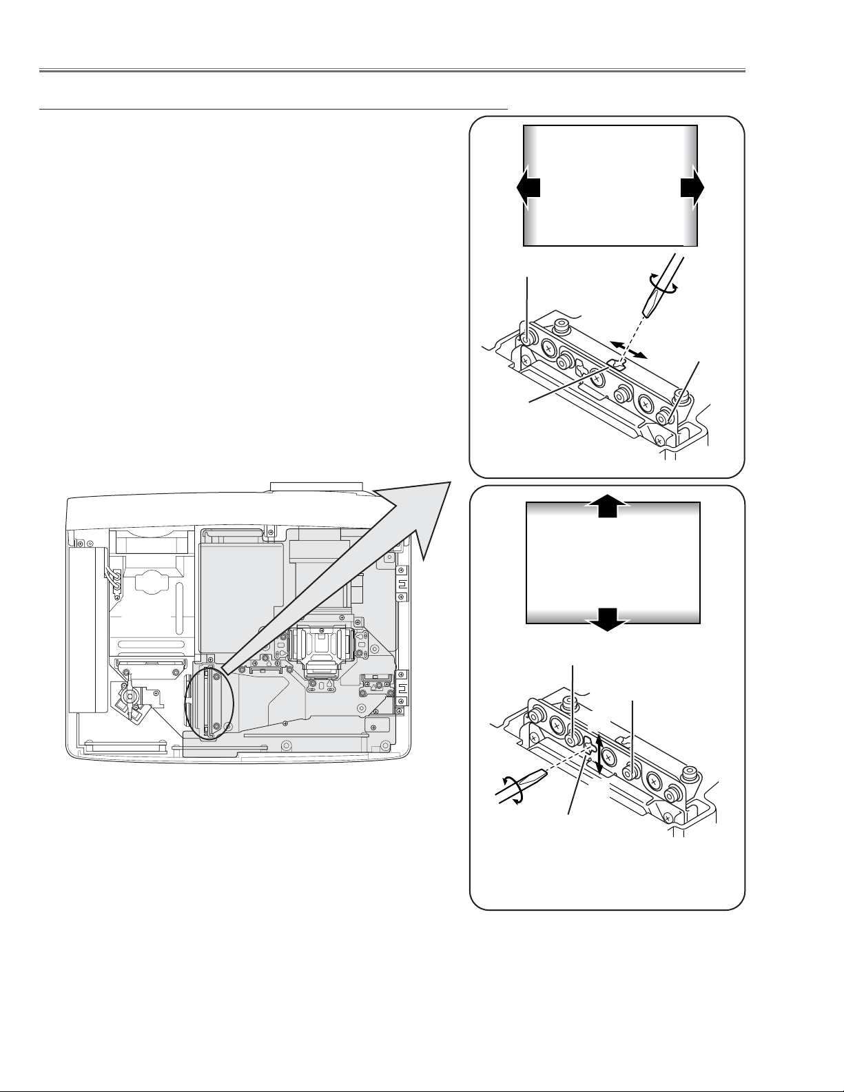
Optical Adjustments
Fig.2-2
1 Turn the projector on by a state of without FPC cables.
2 Project only green light on the screen.
3 Adjust the adjustment base of condenser lens assy to make color
uniformity in green.
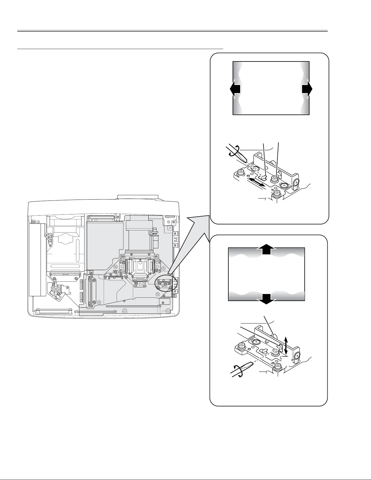
1) If the shading appears on the left or right of the screen as
shown in Fig.2-1, loosen 2 screws A with the 2.0mm hex driver, and adjust the slot B to make color uniformity in green by
using a slot screwdriver.
2) If the shading appears on the top or bottom of the screen as
shown in Fig.2-2, loosen 2 screw C with the 2.0mm hex driver,
and adjust the slot D to make color uniformity in green by using
a slot screwdriver
4 Tighten screws A and C to fix the Condenser lens unit.
Note:
The relay lens adjustment must be carried out after completing this
adjustment.
y
x
Moving of Slot D
Slot D
C
a
b
a
b
Moving of slot B
Fig.2-1
Slot B
A
C
y
x
Green
Green
Condenser Lens adjustment
A
Page 23
-23-
1 Turn the projector on by a state of without FPC cables.
2 Project green and blue lights on the screen.
3 Adjust the adjustment base of condenser lens-out assy to make
color uniformity in cyan.
1) If the shading appears on the left or right of the screen as shown
in Fig.3-1, loosen 1 screw A with the 2.0mm hex driver, and
adjust the slot B to make color uniformity in cyan by using a slot
screwdriver.
2) If the shading appears on the top or bottom of the screen as
shown in Fig.3-2, loosen 1 screw C with the 2.0mm hex driver,
and adjust the slot D to make color uniformity in cyan by using a
slot screw driver.
4 Tighten the screw A and C to fix the relay lens unit.
Fig.3-1
A
Slot B
Optical Adjustments
a
b
b
Moving of slot B
a
Cyan
Fig.3-2
D
Moving of slot D
y
x
C
Condenser Lens-Out adjustment
y
x
Cyan
Page 24
-24-
1 Turn the projector on by a state of without FPC cables.
2 Project all of lights on the screen.
3 Adjust the adjustment base of relay lens assy to make color unifor-
mity in white.
1) If the shading appears on the left or right of the screen as shown
in Fig.4-1, loosen 1 screw A with the 2.0mm hex driver, and
adjust the slot B to make color uniformity in white by using a slot
screwdriver.
2) If the shading appears on the top or bottom of the screen as
shown in Fig.4-2, loosen 1 screw C with the 2.0mm hex driver,
and adjust the slot D to make color uniformity in white by using
a slot screwdriver.
4 Tighten the screws A and C to fix the relay lens unit.
Fig.4-1
A
Slot B
a
b
b
Moving of slot B
a
White
Fig.4-2
Slot D
Moving of slot D
y
x
C
Optical Adjustments
y
x
Relay lens-Out adjustment
White
Page 25
-25-
■ Electrical Adjustments
To enter the service mode
To enter the “Service Mode”, press and hold the MENU and IMAGE button on the projector at the same time for
more than 3 seconds.The service menu appears on the screen as follows.
To adjust service data
Select the adjustment group no.by pressing the MENU button, and select the adjustment item no. by pressing the
pointer UP or DOWN button, and change the data value by pressing the VOLUME – or VOLUME + button. Refer
to the “Service Adjustment Data Table” for further descr iption of adjustment group no., item no.and data value.
To exit the service mode
To exit the ser vice mode, press the POWER ON-OFF button on the projector or remote control unit.
● Service Adjustment Menu Operation
IC1801 on the main board stores the data for the service adjustments, and should not be replaced except for
the case of defective device.
If replaced, it should be performed the re-adjustments
following to the “Electrical Adjustments”.
The data of lamp replacement monitor timer is stored
in the IC1801.
Please note that the lamp replace counter is reset
when the memory IC (IC1801) is replaced.
(Lamp replace counter can not be set to the previous
value.)
● Caution to memory IC replacement
When IC1801 is replaced with new one, the CPU
writes down the default data of the service adjustments
to the replaced IC, refer to the service adjustment
table. As these data are not the same data as factory
shipped data, it should be required to perform the re-
adjustments following to the “Electrical Adjustments”.
Please note that the lamp replace counter is reset.
● Caution of Main Board replacement (in the case
IC1801 is not defective)
When the main board is replaced, IC1801 should be
replaced with the one on previous main board. After
replacement, it should be required to perform the readjustments following to the “Electrical Adjustments”.
In this case, the lamp replace counter can be kept the
v
alue as before.
● Memory IC Replacement
Group No.
Data value
Item No.
Service Mode
Input Video
Group No. Data
0032
Ver. 1 .00
Page 26
-26-
After replacing the Power Board, PF.C. Board, readjust
the Output voltage adjustment as follows.
1. Connect a digital voltmeter to pins 1 (+) and 3 (-) of
K6D.
2. Adjust the voltage by using VR611 as following.
A
C Input Reading
230V 370V ±2V
or 120V 340V ±2V
Caution:
Be sure to connect the lamp when taking this adjustment.
● Circuit Adjustments
CAUTION:The each circuit has been made by the fine adjustment at factory. Do not attempt to adjust the follow-
ing adjustments except requiring the readjustments in servicing otherwise it may cause loss of performance and product safety.
[Adjustment Condition]
● Input signal
Video signal .......................... 1.0Vp-p/75Ω terminated, 16 steps gray scale (Composite video signal)
Computer signal ...................... 0.7Vp-p/75Ω terminated, 16 steps gray scale pattern (XGA)
● Picture control mode ...................... “STANDARD” mode unless otherwise noted.
Note:
* Please refer to “Service Adjustment Menu Operation” for entering to the service mode and adjusting the service
data.
Electrical Adjustments
Output Voltage adjustment
1. Receive the 16-step grey scale video signal.
2. Set to VIDEO mode.
3. Enter the ser vice mode.
[R-PEDESTAL ADJUSTMENT]
4. Connect an oscilloscope to test point “TP201R”(+)
and chassis ground (-).
5. Select group no. “3”, item no. “14” and change data
value to adjust the pedestal lev el and b lack level to be
the same level.
[G-PEDESTAL ADJUSTMENT]
6. Connect an oscilloscope to test point “TP201G”(+)
and chassis ground (-).
7. Select group no. “3”, item no. “15” and change data
value to adjust the pedestal lev el and b lack level to be
the same level.
[B-PEDESTAL ADJUSTMENT]
8. Connect an oscilloscope to test point “
TP201B”(+)
and chassis ground (-).
9. Select group no. “3”, item no. “16” and change data
value to adjust the pedestal lev el and b lack level to be
the same level.
Pedestal adjustment
1. Enter the service mode and select group no. “11” and
item no.“0”. Set data value to “1”.
2. Connect a digital voltmeter to test point “TP12V1” (+)
and chassis ground (-).Select item no .“1” and change
data value to adjust voltage to be 8.0 ±0.1V.
3. Connect a digital voltmeter to test point “TP12V2” (+)
and chassis ground (-). Select item no.“2” and
change data value to adjust voltage to be 9.0 ±0.1V.
4. Select group no. “11” and item no. “0” and set data
value to “3”.
5. Connect a digital voltmeter to test point “TP12V1” (+)
and chassis ground (-).Select item no .“3” and change
data value to adjust voltage to be 13.0 ±0.1V.
6. Connect a digital voltmeter to test point “TP12V2” (+)
and chassis ground (-).Select item no .“4” and change
data value to adjust voltage to be 13.5 ±0.1V.
Fan Voltage adjustment
Pedestal level = Black level
(a)
Page 27
-27-
Electrical Adjustments
1. Receive the 16-step grey scale computer signal.
2. Set to COMPUTER mode.
3. Enter the ser vice mode.
[R-SIGNAL CENTER ADJUSTMENT]
4. Connect a digital voltmeter to test point “TP25R1”(+)
and chassis ground (-).
5. Select group no. “3”, item no. “0” and change data
value to adjust the voltage to be 7.30 ±0.05V.
[G-SIGNAL CENTER ADJUSTMENT]
6. Connect a digital voltmeter to test point “TP25G1”(+)
and chassis ground (-).
7. Select group no. “
3”, item no. “1” and change data
value to adjust the voltage to be 7.30 ±0.05V.
[B-SIGNAL CENTER ADJUSTMENT]
8. Connect a digital voltmeter to test point “TP25B1”(+)
and chassis ground (-).
9. Select group no. “3”, item no. “2” and change data
value to adjust the voltage to be 7.30 ±0.05V.
1. Receive the 16-step grey scale computer signal.
2. Set to COMPUTER mode.
3. Connect an oscilloscope to test point “TP3551” (+)
and chassis ground (-).
4. Enter the ser vice mode, select group no.“3”, item no.
“7” and change data value to adjust amplitude “a” to
be 5.5 ±0.1V.
Signal Center adjustment
NRS adjustment
1. Receive the 16-step grey scale computer signal.
2. Set to COMPUTER mode.
3. Enter the ser vice mode.
[R-BLACK ADJUSTMENT]
4. Connect an oscilloscope to test point “TP25R1” (+)
and chassis ground (-).
5. Select group no.“3”, item no.“3” and change data
value to adjust amplitude “a”to be 10.0 ±0.1V.
[R-BLACK ADJUSTMENT-]
6. Connect an oscilloscope to test point “TP25G1” (+)
and chassis ground (-).
7. Select group no.“3”, item no.“4” and change data
value to adjust amplitude “a”to be 10.0 ±0.1V.
[R-BLACK ADJUSTMENT-]
8. Connect an oscilloscope to test point “TP25B1” (+)
and chassis ground (-).
9. Select group no.“3”, item no.“5” and change data
value to adjust amplitude “a”to be 10.0 ±0.1V.
Black Level adjustment
(a)
black level
(a)
black level
Page 28
-28-
Electrical Adjustments
1. Receive the 16-step gray scale computer signal.
2. Set to COMPUTER mode.
3. Enter the ser vice mode.
[R-GAIN ADJUSTMENT]
4. Connect an oscilloscope to test point “TP25R1”(+)
and chassis ground (-).
5. Select group no.“2”, item no.“3” and change data
value to adjust waveform “a”to be minimum amplitude.
[G-GAIN ADJUSTMENT]
6. Connect an oscilloscope to test point “TP25G1”(+)
and chassis ground (-).
7. Select group no.“2”, item no.“4” and change data
value to adjust waveform “a”to be minimum amplitude.
[B-GAIN ADJUSTMENT]
8. Connect an oscilloscope to test point “TP25B1”(+)
and chassis ground (-).
9. Select group no.“2”, item no.“5” and change data
value to adjust waveform “a”to be minimum amplitude.
PC Gain adjustment
1. Receive the 16-step gray scale computer signal.
2. Set to COMPUTER mode.
3. Enter the ser vice mode.
[R-OFFSET ADJUSTMENT]
4. Connect an oscilloscope to test point “TP25R1”(+)
and chassis ground (-).
5. Select group no.“3”, item no.“11” and change data
value to adjust the waveform “a” (black portion ) to
be maximum amplitude.
[G-OFFSET ADJUSTMENT]
6. Connect an oscilloscope to test point “TP25G1”(+)
and chassis ground (-).
7. Select group no.“3”, item no.“12” and change data
value to adjust the waveform “a” (black portion ) to
be maximum amplitude.
[B-OFFSET ADJUSTMENT]
8. Connect an oscilloscope to test point “TP25B1”(+)
and chassis ground (-).
9. Select group no.“3”, item no.“13” and change data
value to adjust the waveform “a” (black portion ) to
be maximum amplitude.
PC Offset adjustment
Black Level
(a)
White Level
(a)
Page 29
-29-
Electrical Adjustments
[PC-GAMMA OFF ADJUSTMENT]
1. Receive the 16-step gray scale computer signal.
2. Set to COMPUTER mode.
3. Enter the service mode, select group no. “2”, item
no.“6”and change data value to reproduce the proper gray scale picture on the screen.
[AV-GAMMA OFF ADJUSTMENT]
4. Receive the 16-step gray scale video signal.
5. Set to VIDEO mode.
6. Enter the service mode, select group no. “2”, item
no.“6”and change data value to reproduce the proper gray scale picture on the screen.
1.Receive the 1 dot black & white pattern computer signal.
2. Set to COMPUTER mode.
3. Enter the service mode.
[G-COMMON CENTER ADJUSTMENT]
4. Project only green light component to the screen.
5. Select group no.“3”, item no.“8” and change data
value to obtain the minimum flicker on the screen.
[B-COMMON CENTER ADJUSTMENT]
6. Project only blue light component to the screen.
7. Select group no.“3”, item no.“9” and change data
value to obtain the minimum flicker on the screen.
[R-COMMON CENTER ADJUSTMENT]
8. Project only red light component to the screen.
9. Select group no.“3”, item no.“10” and change data
value to obtain the minimum flicker on the screen.
Gamma Shift adjustment
Common Center adjustment
1. Receive the 16-step gray scale video signal.
2. Set to VIDEO mode.
3. Enter the ser vice mode.
[R-GAIN ADJUSTMENT]
4. Connect an oscilloscope to test point “TP25R1”(+)
and chassis ground (-).
5. Select group no.“2”, item no.“3” and change data
value to adjust waveform “a”to be minimum amplitude.
[G-GAIN ADJUSTMENT]
6. Connect an oscilloscope to test point “TP25G1”(+)
and chassis ground (-).
7. Select group no.“2”, item no.“4” and change data
value to adjust waveform “a”to be minimum amplitude.
[B-GAIN ADJUSTMENT]
8. Connect an oscilloscope to test point “TP25B1”(+)
and chassis ground (-).
9. Select group no.“2”, item no.“5” and change data
value to adjust waveform “a”to be minimum amplitude.
AV Gain adjustment
[PC WHITE BALANCE ADJUSTMENT]
1. Receive the 16-step gray scale computer signal.
2. Set to COMPUTER mode.
3. Enter the service mode, select group no.“2”, item no.
“7” (Red) or “8” (Blue), and change data values
respectively to make a proper white balance.
[A V WHITE BALANCE ADJUSTMENT]
4. Receive the 16-step grey scale video signal.
5. Set to VIDEO mode.
6. Enter the service mode, select group no.“2”, item no.
“7” (Red) or “8” (Blue), and change data values
respectively to make a proper white balance.
Confirm that the same white balance is obtained in
video and computer input.
White Balance adjustment
If you find the color shading on the screen, please
adjust the white uniformity by using the proper computer and “Color Shading Correction” software supplied
separately.
NOTE ON WHITE UNIFORMITY
ADJUSTMENT
(a)
White Level
Page 30
Group: 0 TB1274
0 TINT 32 0 ~ 63
1 SHP_EQ 2 0 ~ 3
2 SHP_FO 1 0 ~ 3
NTSC,PAL SECAM,NT4.43 S-Video Y,Cb,Cr
3 SHP_GAIN 10 10 10 10 0 ~ 15
NTSC NT4.43 PAL SECAM
4 Y_OUT_LEVEL 30 30 31 31 0 ~ 63
S-Video NTSC S-Video PAL S-Video SECAM Y,Cb,Cr
30 31 31 31
NTSC NT4.43 PAL SECAM
5 C_OUT_LEVEL 32 32 32 32 0 ~ 63
S-Video NTSC S-Video PAL S-Video SECAM Y,Cb,Cr
32 32 32 32
NTSC PAL SECAM NT4.43 PAL 60
6 Y_DELAY 6 6 6 4 4 0 ~ 15
S-Video NTSC S-Video PAL S-Video SECAM S-Video NT4.43 S-Video PAL60
443 34
7 COL_SYS - -
8X’TAL - -
9 NOISE_DET - -
10 V_FREQ - - Read only
11 Vert. Std - -
12 CID - -
13 V_SIG - -
NTSC,PAL SECAM,NT4.43 S-Video YCbCr
14 Cinema SHP_GAIN 8 8 8 8 0 ~ 15 For cinema mode
Group: 1 CXA2101
0 PICTURE 30 0 ~ 63
1 BRIGHT 31 0 ~ 63
2 R_DRIVE 31 0 ~ 63
3 G_DRIVE 31 0 ~ 63
4 B_DRIVE 31 0 ~ 63
5 HSEP_SEL 1 0 ~ 1
6 CR_OFFSET1 15kHz: 7 Others: 10 0 ~ 15
7 CB_OFFSET1 15kHz: 7 Others: 10 0 ~ 15
8 BLK_BOTTOM 15 0 ~ 15
NTSC PAL, SECAM 1035i Y,Cb,Cr *1 *1 Y, Cb, Cr and Y, Pb, Pr except 1035i
9 R-Y/R 6 13 6 6 0 ~ 15
10 R-Y/B 5 15 5 5 0 ~ 15
11 G-Y/R 8 8 8 8 0 ~ 15
12 G-Y/B 10 4 10 10 0 ~ 15
13 MAT_OUT 0 0 0 1 0 ~ 3
15kHz 480i, 575i 480p, 575p 1080i, 1035i, 720p
14 SYSTEM 0 1 2 0 ~ 3
15 V_TC 3 3 3 0 ~ 3
16 H_WIDTH 3 2 0 0 ~ 3
17 HS_MASK 0 1 1 0 ~ 1
Video, S-Video 480i, 575i 480p, 575p 1080i, 1035i, 720p
18 CTI_LEVEL 2 2 2 2 0 ~ 3
15kHz 480i, 575i 480p, 575p 1080i, 1035i, 720p
19 SUB_SHP 3 3 3 0 ~ 3
20 SHP_FO 0 2 3 0 ~ 3
21 PRE_OVER 2 2 3 0 ~ 3
22 LTI_LEVEL 0 1 1 0 ~ 3
23 D_PIC 0 0 0 0 ~ 3
24 HUE 31 0 ~ 63 Only adjustable for PAL,SECAM
NTSC PAL,SECAM 525i,480p 625i,575p 1035i Others
25 SUB_COL 5 5 12 12 6 9 0 ~ 15
26 SUB_HUE 7 7 8 7 9 6 0 ~ 15
27 Cinema CTI_LEVEL 2 0 ~ 3 Set this value at Cinema Mode
-30-
Electrical Adjustments
● Service Adjustment Data Table
These initial values are the reference data written from the CPU
ROM to memory IC when replaced new memory IC.The adjustment items indicated with “✻” are required to readjust following
to the “Electrical adjustments”. Other items should be used with
the initial data value.
No. Adjustment Item Initial Value Range Description
Page 31

28 Cinema LTI_LEVEL 0 0 ~ 3 Set this value at Cinema Mode
Group: 2 L3E07050 (Digital Gamma, Color Shading & Timing Controller)
PC DVI,AV
0 R_SUB_BRT 0 0 0 ~ 1023
1 G_SUB_BRT 0 0 0 ~ 1023
2 B_SUB_BRT 0 0 0 ~ 1023
PC AV DVI
3R_SUB_GAIN 573 573 492 0 ~ 1023 ✻ Red PC/AV gain adjustment
4 G_SUB_GAIN 573 573 492 0 ~ 1023 ✻ Green PC/AV gain adjustment
5 B_SUB_GAIN 573 573 492 0 ~ 1023 ✻ Blue PC/AV gain adjustment
PC, DVI Standard AV Standard
6 Standard G GAMMA SHIFT 415 415 Note1 ✻ Gamma shift adjustment
7 Standard R GAMMA SHIFT 415 415 Note1 ✻ White balance adjustment
8
Standard B GAMMA SHIFT 415 415 Note1
✻ White balance adjustment
9 Standard GAMMA 0 0 0 0 ~ 1023
10 Standard GAMMA 1 210 166 0 ~ 1023
11 Standard GAMMA 2 340 290 0 ~ 1023
12 Standard GAMMA 3 436 406 0 ~ 1023
13 Standard GAMMA 4 511 496 0 ~ 1023
14 Standard GAMMA 5 574 560 0 ~ 1023
15 Standard GAMMA 6 633 626 0 ~ 1023
16 Standard GAMMA 7 674 672 0 ~ 1023
17 Standard GAMMA 8 709 709 0 ~ 1023
18 Standard GAMMA 9 740 740 0 ~ 1023
19 Standard GAMMA 10 770 770 0 ~ 1023
20 Standard GAMMA 11 800 800 0 ~ 1023
21 Standard GAMMA 12 832 838 0 ~ 1023
22 Standard GAMMA 13 884 877 0 ~ 1023
23 Standard GAMMA 14 950 940 0 ~ 1023
24 Standard GAMMA 15 1023 1023 0 ~ 1023
PC, DVI Real AV Cinema (Different value to Standard)
25
Real/Cinema G GAMMA SHIFT 506 507 Note1 Note1:
26
Real/Cinema R GAMMA SHIFT 512 512 Note1
27 Real/Cinema B GAMMA SHIFT 504 504 Note1
28 Real/Cinema GAMMA 0 512 512 0 ~ 1023
29 Real/Cinema GAMMA 1 492 538 0 ~ 1023
30 Real/Cinema GAMMA 2 497 524 0 ~ 1023
31 Real/Cinema GAMMA 3 502 519 0 ~ 1023
32 Real/Cinema GAMMA 4 507 516 0 ~ 1023
33 Real/Cinema GAMMA 5 509 515 0 ~ 1023
34 Real/Cinema GAMMA 6 510 512 0 ~ 1023
35 Real/Cinema GAMMA 7 510 511 0 ~ 1023
36 Real/Cinema GAMMA 8 510 510 0 ~ 1023
37 Real/Cinema GAMMA 9 510 510 0 ~ 1023
38 Real/Cinema GAMMA 10 510 510 0 ~ 1023
39 Real/Cinema GAMMA 11 509 510 0 ~ 1023
40 Real/Cinema GAMMA 12 508 510 0 ~ 1023
41 Real/Cinema GAMMA 13 506 509 0 ~ 1023
42 Real/Cinema GAMMA 14 502 502 0 ~ 1023
43 Real/Cinema GAMMA 15 512 512 0 ~ 1023
44 R 2 127 0 ~ 255 R Correction value of vertical line
45 G 2 127 0 ~ 255 G Correction value of vertical line
46 B 2 127 0 ~ 255 B Correction value of vertical line
47 Red MID2 Level 453 0 ~ 1023
48 Red MID1 Level 500 0 ~ 1023
49 Red MAX Level 576 0 ~ 1023
50 Green MID2 Level 453 0 ~ 1023 Gray scale level adjustment
51 Green MID1 Level 500 0 ~ 1023
52 Green MAX Level 575 0 ~ 1023
53 Blue MID2 Level 418 0 ~ 1023
54 Blue MID1 Level 465 0 ~ 1023
55 Blue MAX Level 541 0 ~ 1023
56 DVI std G GAMMA SHIFT 512 0 ~ 1023
57 DVI std R GAMMA SHIFT 512 0 ~ 1023
58 DVI std B GAMMA SHIFT 512 0 ~ 1023
Group: 3 DAC
0R_VIDEO_CENTER 74 0 ~ 255 ✻ Red Signal center adjustment
1 G_VIDEO_CENTER 74 0 ~ 255 ✻ Green Signal center adjustment
2 B_VIDEO_CENTER 74 0 ~ 255
✻ Blue Signal center adjustment
-31-
Electrical Adjustments
No. Adjustment Item Initial Value Range Description
Page 32

3 REF_R 136 0 ~ 255 ✻ Red white-black level adjustment
4 REF_G 136 0 ~ 255 ✻ Green white-black level adjustment
5 REF_B 136 0 ~ 255 ✻ Blue white-black level adjustment
6 NRS_B 128 0 ~ 255
7 NRS_A 190 0 ~ 255 ✻ NRS adjustment
8 G_V_COM 140 0 ~ 255 ✻ Green common center adjustment
9 B_V_COM 140 0 ~ 255 ✻ Blue common center adjustment
10 R_V_COM 140 0 ~ 255 ✻ Red common center adjustment
11 R_CLMP 63 0 ~ 255 ✻ Red PC offset adjustment
12 G_CLMP 63 0 ~ 255 ✻ Green PC offset adjustment
13 B_CLMP 63 0 ~ 255 ✻ blue PC offset adjustment
14 R_BLK_DC 76 0 ~ 255 ✻ Red pedestal adjustment
15 G_BLK_DC 76 0 ~ 255 ✻ Green pedestal adjustment
16 B_BLK_DC 76 0 ~ 255 ✻ blue pedestal adjustment
Group: 4 TA1318
15kHz 31kHz 33kHz 45kHz
0 SEP_LEV 0 0 0 0 0 ~ 3
1080i 720p 480p 575i,PAL,SECAM 480i,NTSC
1 HD_PHASE 36 38 36 32 32 0 ~ 63
2 V_FREQ - - Read only
3H_FREQ - -
4 HD_IN - -
Group: 5 LP05 (Turbo)
0 LP05_R_GAIN 128 0 ~ 255
1 LP05_G_GAIN 128 0 ~ 255
2 LP05_B_GAIN 128 0 ~ 255
3 TURBO_GAIN 19 0 ~ 255
Group: 10 Option
0 Lamp Time Monitor - - Read only
1 RS232C Baudrate 0 0 ~ 1 0: 19200bps 1: 9600bps
2 Shootout Mode 0 0 ~ 2
1:Mode-1(Change when no signal input) 2:Mode-2(Priority of AV) 0: Disable
3 Cooling Time 3 0 ~ 15 Set cooling time period 1:30 sec. 3:90 sec. 15:450 sec. 0:On conti.
4High-Land SW 0 0 ~ 1 0: Normal mode(Normal operation) 1:Highland mode(max speed in nor mal)
5V-Sync SW 0 0 ~ 1 0:Vertical-synchronized 1:No vertical-synchronized
6 Color Shading SW 1 0 ~ 1 Color correction 0: No 1:Yes, adjustable but does no store the value
7MCI Output Auto 1 0 ~ 1 Auto: 1, Fixed: 0
6Keystone Option 0 0 ~ 1 Fixed limitation :0, Change limitation to the input: 1
Group: 11 Fan Control ✻ Fan voltage adjustment
0Fan Speed Mode 0 0 ~ 3 0: Fan control 1: Min., 2:Mid., 3: Max. it can not be memorized.
1Fan-1 Min Data 44 0 ~ 127 Minimum output data when controlling Fans ✻
2Fan-2 Min Data 63 0 ~ 127 Minimum output data when controlling Fans ✻
3Fan-1 Max Data 217 128 ~ 255 Maximum output data when controlling Fans ✻
4Fan-2 Max Data 236 128 ~ 255 Maximum output data when controlling Fans ✻
5Temp Low 37 10 ~ 80 Decides output data of DAC for temperature
6Temp High 45 30 ~ 80 Decides output data of DAC for temperature
7Fan-1 Temp Error 61 30 ~ 80 Temperature which CPU judges the abnormal temperature
(optical unit temperature, on Main board)
8Fan-2 Temp Error 51 30 ~ 80 Temperature which CPU judges the abnormal temperature
(outside temperature, on Temp board)
9Fan-1 Speed Monitor - 0 ~ 255 Read only, displays DAC output data
10 Fan-2 Speed Monitor - 0 ~ 255 Read only, displays DAC output data
11 Temp Monitor - 0 ~ 9999 Read only ( Upper 2 byte indicates for Fan-1.
Lower 2 byte indicates Fan-2)
12 Eco mode Fan-1 Min Data 44 0 ~ 127 decides minimum output data at Eco mode.
13 Eco mode Fan-2 Min Data 63 0 ~ 127 decides minimum output data at Eco mode.
14
Eco mode Fan-1 Max Data 217 128 ~ 255 decides maximum output data at Eco mode.
15 Eco mode Fan-2 Max Data 236 128 ~ 255 decides maximum output data at Eco mode.
Group: 12 PC Real / AV Cinema
0 PC Real Contrast 32 0 ~ 63
1 PC Real Br ightness 32 0 ~ 63
2 PC Real Red 32 0 ~ 63
3 PC Real Green 32 0 ~ 63
4PC Real Blue 32 0 ~ 63
5 PC Real Gamma 8 0 ~ 15
6AV Cinema Contrast 32 0 ~ 63
7AV Cinema Brightness 32 0 ~ 63
8AV Cinema Color 32 0 ~ 63
9AV Cinema Tint 32 0 ~ 63
10 AV Cinema Red 32 0 ~ 63
-32-
Electrical Adjustments
No. Adjustment Item Initial Value Range Description
Page 33

11 AV Cinema Green 32 0 ~ 63
12 AV Cinema Blue 32 0 ~ 63
13 AV Cinema Sharpness 15 0 ~ 31
14 AV Cinema Gamma 8 0 ~ 15
Group: 500 ADC
0 ADC R-OFFSET 64 0 ~ 255
1 ADC G-OFFSET 64 0 ~ 255
2 ADC B-OFFSET 64 0 ~ 255
3 ADC R-GAIN 254 0 ~ 255
4ADC G-GAIN 254 0 ~ 255
5 ADC B-GAIN 254 0 ~ 255
Group: 510 NTSC Gakaku
0 NTSC TOTAL DOTS 2626 0 ~ 2047
1 NTSC DISP DOTS 1024 0 ~ 2047
2 NTSC H BACK PORCH 230 0 ~ 2047
3 NTSC V BACK PORCH 46 0 ~ 2047
4 NTSC DISP LINE 456 0 ~ 2047
5 NTSC CLAMP 4 0 ~ 2047
Group: 511 PAL Gakaku
0PAL TOTAL DOTS 2690 0 ~ 2047
1PAL DISP DOTS 1024 0 ~ 2047
2PAL H BACK PORCH 266 0 ~ 2047
3PAL V BACK PORCH 62 0 ~ 2047
4PAL DISP LINE 533 0 ~ 2047
5PAL CLAMP 4 0 ~ 2047
Group: 512 HDTV 1080i-60 Gakaku
0TOTAL DOTS 1206 0 ~ 2047
1 DISP DOTS 1024 0 ~ 2047
2H BACK PORCH 145 0 ~ 2047
3V BACK PORCH 52 0 ~ 2047
4 DISP LINE 1048 0 ~ 2047
5 CLAMP 5 0 ~ 2047
Group: 513 HDTV 1080i-50 Gakaku
0TOTAL DOTS 1448 0 ~ 2047
1 DISP DOTS 1024 0 ~ 2047
2H BACK PORCH 144 0 ~ 2047
3V BACK PORCH 64 0 ~ 2047
4 DISP LINE 1044 0 ~ 2047
5 CLAMP 5 0 ~ 2047
Group: 514 HDTV 1035i Gakaku
0TOTAL DOTS 1206 0 ~ 2047
1 DISP DOTS 1024 0 ~ 2047
2H BACK PORCH 145 0 ~ 2047
3V BACK PORCH 90 0 ~ 2047
4 DISP LINE 1006 0 ~ 2047
5 CLAMP 5 0 ~ 2047
Group: 515 HDTV 720p Gakaku
0TOTAL DOTS 1354 0 ~ 2047
1 DISP DOTS 1024 0 ~ 2047
2H BACK PORCH 260 0 ~ 2047
3V BACK PORCH 36 0 ~ 2047
4 DISP LINE 698 0 ~ 2047
5 CLAMP 5 0 ~ 2047
Group: 516 HDTV 575p Gakaku
0TOTAL DOTS 1348 0 ~ 2047
1 DISP DOTS 1024 0 ~ 2047
2H BACK PORCH 240 0 ~ 2047
3V BACK PORCH 60 0 ~ 2047
4 DISP LINE 524 0 ~ 2047
5 CLAMP 0 0 ~ 2047
Group: 517 HDTV 480p Gakaku
0TOTAL DOTS 1288 0 ~ 2047
1 DISP DOTS 1024 0 ~ 2047
2H BACK PORCH 212 0 ~ 2047
3V BACK PORCH 46 0 ~ 2047
4 DISP LINE 451 0 ~ 2047
5 CLAMP 0 0 ~ 2047
No. Adjustment Item Initial Value Range Description
-33-
Electrical Adjustments
Page 34

-34-
Electrical Adjustments
● MAIN BOARD
Test Points and Locations
TP3551
TP25R1
TP11SC
K25R
TP25R2
TP11SY
TP25G1
TP25G2
TP11CV
K25G
TP11PB
TP11PR
TP62V
IC4101
TP25B1
TP62H
K25B
TP52R
TP201G
TP25B2
TP52G
TP52B
TP201B
TP201R
TP205
IC301
TP12V2
TP12V1
TPDCLK
TPDVS
TPDHS
TP3581
IC401
IC801
K8P
Page 35

-35-
■ Troubleshooting
No Power
The possible causes of No Power are listed below.Please
check following and refer to power supply and protection circuits diagram in the figure opposite.
1. Stop the operation of power supply circuit due
to detection of abnormality
.
- Detected the abnormality on the secondary power supply
lines.
Power failure detection diodes detect an abnormal voltage on the power supply. Check the shortage of secondary circuits, ICs, condensers, etc.
- Detected the operation stop of cooling fans.
Power failure detection diodes detect the fan operation
stop.Check Fans FN901, FN902, FN903, FN904, FN905
and FN906
Check fan's power supply lines and detection diodes and
transistors D69A, D69B, D69C and Q69A
- Detected the abnormal temperature rise inside the projec-
tor.
Temperature sensor ICs detect abnormal temperature.
Check peripheral circuits and sensor ICs IC4881 and
IC2881.
Thermal switch (TSW611) detects abnormal temperature.
Check peripheral circuits and TSW611.
TSW611.................... open in normal
TSW611 shorts when the peripheral temperature is over
90°C.
Thermal switch (SW902) detects abnormal temperature.
Check peripheral circuits and SW902.
SW902...................... short in normal
SW902 opens when peripheral temperature is over
100°C.
- Detected the abnormality on the lamp ballast unit.
The lamp ballast unit outputs error signal (LAMP_ERR)
to pin 47 of IC801.
LAMP_ERR .............. High in abnormal
- Detected the over load/over voltage on power supply circuit.
Feedback circuits detect over load or over voltages.
Check PC641, PC642 and peripheral circuits.
- Operated the mechanical protect on the Interlock switch
(SW904). Check lamp cover fixed correctly.
- Fuse (F601) open.
2. Abnormality occurs on drive signals for power
or lamp circuit.
- Abnormality on power starter signals (POWER, 5V_SW).
POWER signal is output from pin 1 of IC801 and sent to
pin 17 of IC1881, and output from pin 3 by the name of
5V_SW signal. 5V_SW signal drives 15.5V and 9VMCI
power supply circuits on the power board.
POWER/5V_SW ............ High in power on
Check POWER and 5V_SW signals, 9V regulator circuit
Q65A, Q65B, Q65C, IC65A and peripheral circuit, 15.5V
switch circuit Q661, Q662 and peripheral circuit on the
Power Board.
- Abnormality on lamp ballast drive signal (BALLAST_AC).
BALLAST_AC signal is output from pin 39 of IC801 and
sent to pin 11 of IC1881, and output from pin 9 by the
name of BALLAST_AC1 signal. BALLAST_SW1 signal
drives the lamp ballast unit.
Check BALLAST_AC and BALLAST_AC1 signals and
lamp ballast unit.
- Abnormality on fan drive signal (FAN DRIVE).
FAN DRIVE signal is output from pin 41 of IC801 and
sent to pin 15 of IC1881, and output from pin 5 by the
name of FAN DRIVE1 signal. FAN DRIVE1 signal drives
fan supply voltages (12V/12V1) on the power board.
FAN DRIVE/
FAN DRIVE1 .............. High in power on
Check FAN DRIVE/FAN DRIVE1 signals, 12V regulator
circuits IC681, Q681, Q682, Q66A, IC671, Q671, Q672
and peripheral circuits.
- Abnormality on power drive signal (LAMP_BST_SW).
LAMP_BST_SW signal is output from pin 82 of IC801
and sent to pin 2 of IC1871, and output from pin 18 by
the name of LAMP_BST_SW1 signal. LAMP_BST_SW1
signal drives the power factor control IC on the P.F. board
through the Power board.
LAMP_BST_SW/
LAMP_BST_SW1............ High in power on
Check LAMP_BST_SW and LAMP_BST_SW1 signal,
photo-coupler PC643, transistors Q651, Q641 and
peripheral circuits.
3. Abnormality occurs on the power circuit.
- Abnormality on power primary circuit
Check Line filters, L601, L602, D614, L611, IC631, D632,
etc.
- Abnormality on power secondary circuit
Check D651, D652, D653, IC651, etc.
Page 36

-36-
Troubleshooting
Power supply drive and protection diagrams and locations
SW902
F601
SW904
IC2881
IC4881
AC IN
FN901FN902
FN903
Power
Oscillator
Circuit
15.5V
P.F BOARD
K6D
K6E
147
4
1
TSW611
7
K6F
K6S K8S
LAMP_BST_SW1
On: High
K6S K8S
On: High
On: High
37-38
13-14
9-10
15-16
11-12
IC611
P.F.CONTROL
Failure: Low Failure: Low
1
2
1
2
FN904
F601
Fuse
K6J
K6K
K6M
K6L
SW902
Thermal sw.
Fan Control
IC681IC671
Interlock sw.
15.5V
6V
-6V
Q661
SW904
POWER BOARD MAIN BOARD
LAMP BALLAST UNIT
11
CB1
3
3
CB2
1 3
1
K8B
LAMP_BST_SW1
LAMP
LAMP_SW1
BALAST_AC1
5V_SW5V_SW
FAN DRIVE1FAN DRIVE1
3
LAMP_ERR
FN905
FN906
1 2
K8N
K8P
P-FAILP-FAIL
BUFFER
BUFFER
IC1871
18 2
IC1881
12
9
3
LAMP Ass'y
Failure: High
On: High
On: Low
8
11
On: High
17
On: High
15
47 80 81
48
82
3
39
1
415
TEMP. SENS.
3
5
K48E
TEMP. SENSOR
53
K8E
SCL
SDA
TEMP.SENSOR
IC801
SUB CPU
IC4881
1
2
BOARD
IC2881
1
2
Page 37

-37-
The possible causes of No Picture are listed below. Please
check following and refer to video signal processing diagrams in the figure opposite.
1. No picture from Video source
Composite Video Input
Check composite video signal at pins 45 and 46 of K10U
on AV Board and K3U on Main Board.
Check Y, C signals at pins 7 and 9 of IC2101.
Check Y, C signals at pins 5 and 7 of IC1101
S-Video Input
Check S-video signals at pins 39, 40 (Y), 41, 42 (C) of
K10U and K3U.
Check Y, C signals at test points TP11SC and TP11SY.
Check Y, C signals at pins 43 and 44 of IC1101.
Component Input
Check component signals at pins 49, 50(Pb), 51, 52 (Pr)
of K10U and K3U.
Check component signals (Y, Pr, Pb) at test points
TP11CV, TP11PB and TP11PR.
All of video signals
Check component signals (Y, Cr, Cb) at pins 21, 22 and
23 of IC1101.
Check component signals (Y, Cr, Cb) at pins 67, 68 and
69 of IC4101.
Check component signals (Y, Pr, Pb) at pins 73, 74 and
75 of IC4101.
Check Sync signals (AV_HSYNC, AV_VSYNC) at pins 4
and 9 of IC1101.
Check Sync signals (AV_HSYNC, AV_VSYNC) at pins 65
and 66 of IC4101.
Check RGB signals at pin 35, 37 and 39 of IC4101.
Check RGB signals at pins 14, 4 and 15 of IC3101.
Check blanking signal at pin 9, 10, 11 of IC3101.
Check RGB signals at pins 1, 3 and 5 of IC5241.
Check Sync signals (AV_HSYNC, AV_VSYNC) at pins 2
and 12 of IC6261.
Check AV/PC switching signal at pin 22 of IC5241 and
pins 10 and 11 of IC6261.
AV :Low, PC : High
2.
No picture from Computer source
Check RGB signals at pins 3-4, 7-8 and 11-12 of K10T on
AV Board and K3T on Main Board.
Check Sync signals (PC_HSYNC, PC_VSYNC) at pins
15-16 and 19-20) of K10T on AV Board and K3T on Main
Board.
Check RGB signals at pins 12, 10 and 8 of IC5241.
Check Sync signals at pins 1 and 13 of IC6261.
Check AV/PC switching signal at pin 22 of IC5241 and
pins 10 and 11 of IC6261.
AV :Low, PC : High
3.
No picture from both of Video and Computer
sources.
Check RGB signals at test points TP52R, TP52G and
TP52B.
Check RGB signals at test points TP201R, TP5201G and
TP201B.
Check HSYNC signal at test point TP205.
Check Sync signals at test points at TP62H and TP62V.
4. No picture from all of sources
Check RGB S&H signals at test points TP25B1, TP25B2,
TP25G1, TP25G2, TP25R1 and TP25R2.
Check NRS signals at test points TP3551 and TP3581.
Check power supply circuit 15.5V and 15VL and peripheral circuit.
Check ICs IC501, IC531, IC561, IC1501, IC1531, IC1561,
IC3501, IC3531, IC3561, IC801, IC301, IC401and peripheral circuits.
Troubleshooting
No Picture
SIGNAL K10T/K3T
V-Sync 19-20
H-Sync 15-16
B 11-12
G 7-8
R 3-4
SIGNAL K10U/K3U
Video 45-46
S-C 41-42
S-Y 39-40
PB 49-50
PR 51-52
Page 38

-38-
Troubleshooting
Video Signal processing diagrams
TP25B1
TP25B2
K25B
IC501
B-LCD
IC1501
S&H_B
B
IC5241
IC5211
PANEL
TP25G1
DBB0-9
IC401
7
TP201R
TP201G
R
G
IC5281
IC5271
TP52R
TP52G
20
8
12
10
AV/PC-RGB
B
R
G
RGB
151210
257
RGB-AMP.
3
7
11
RGB
ANALOG
K25G
TP25G2
DIGITAL
DGB0-9
IC1401
DB0-9
GB00-7
GBE0-7
15
TP201B
B
IC5291
TP52B
18
R
IC531
DGB0-9
COLOR
DGA0-9
DIGITAL
DG0-9
GG00-7
GGE0-7
IC201
22
16
315
G
G-LCD
PANEL
TP3551
22
SHIFT
IC3531
G_LEVEL
NRS
IC3551
IC1531
S&H_G
DRB0-9
G
6,7 13
TIMING
CONTROL
UNIFORMITY
CORRECTION
DRA0-9
5,4 9,1
CONTROL
BRIGHTER
DR0-9
IC301
SCAN
GR00-7
GRE0-7
SYSTEM
CONVERTER
TPDHS
CONTROL
A/D
40
IC6271
HSYNC
TP205
AV/PC
IC251
IC5251
HAFC
13
2
1
DET
AFC
IC6171
16 17
PC: H
AV : L
22
AV/ PC
B
IC6241
6
3
TP25R1
TP25R2
IC561
DHS/DVS
TPCLK
TPDVS
244
323
34
H
HS
TP62H
TP62V
3
2
BUFFER
15
2
1
SYNC-SW
H
12
1
IC6251
INVERTER
V
H
13
235
SYNC DET.
IC6211
19
15
16
V-SYNC
H-SYNC
IC1561
R
TURBO_1
240
133
V
VS
6
5
14
13
12
V
8
5
11
IC6221
K3T
20
K10T
R-LCD
PANEL
K25R
IC3561
R/B_LEVEL
S&H_R
IC1581
DCLK
10 11
22
SHIFT
RGT
DWN
14
2
D/A
PC: H
AV/ PC
AV BOARD MAIN BOARD
|
3
AV : L
19
H
TP3581
7
3
V
IC3581
NRS
VCOM
5
7
|
2
D/A
IC2571
AV-RGB
NRS
12
3
13
IC6101
IC801
79,78
SCL2_5
BLANK_SW
15
13
D/A
7
4,5,6
7
Pr
515249
Pr/Cr
Pb
IC2161
Y
C
Y
50
Pb/Cb
AV/PC
PC: H
AV : L
7
9
Cb_SW
Cr_SW
INVERTER
AV_HSYNC
AV_VSYNC
TP11SC
IC3101
55 56
HD_HSYNC
8
13
9
13 14
TP11SY
K3U
RGB
IC3121
15
1
BLANKING
R
G
393735
RGB
IC4101
66
6529286968
HD_VSYNC
HS_OUT
4
12
10
1
5
11
4
IC1101
4344171819
Cr
Y/C
TP11PR
39
41
K10U
Y/C
S_SW
S-VIDEO
IC2131
IC3141
4
3
13
2512
B
MATRIX
VS_OUT
Y
Cb
212223
VIDEO
DECODER
Cb
TP11CV
TP11PB
14
9,10
73 74 75
67
Cr
75
CV/Y
SUB
CPU
SDA2_5
8
8
SYNC_SW
IC2101
COMB
DIGITAL
2
CV
45
46
VIDEO/Y
9,18,19
BLKC_DC
FILTER
IC5161
11
C_SWIN
Component-In: H
C_SWIN
353633
2
3
IC2181
12
S_SW
S-In: H
34
I/O
Page 39

-39-
1. No drive signals supplied at motors
Check drive signals at pins 1 to 4 of K6U on Power Board.
Check ICs IC5501, IC5551 and peripheral circuits. Check
motor drive power supply (9VMCI).
2. No drive signals supplied at motor drive ICs.
Check drive signals at pins 3-4 (ZOOM), 5-6 (FOCUS) of
k6S. Check IC801.
3. No drive signals output from CPU.
Check drive signals at pins 29,30, 33, 34 of IC801(SUB
CPU). Check IC801.
4. No key switch signals input to CPU.
Check signals at pins 50 to 52 of IC801 when pressing the
key buttons.Check key buttons.
Troubleshooting
Logic Table of IC5501/IC5551
Input Output Operation
4571
HL LHForward drive
LHHLReverse drive
HH LLBraking
LL --Stand by
Lens Motor Problems
No Sound
1. No audio signals at A
V input circuit.
Check audio signals at pins14 and 15 of IC5011 on AV
Board. Check IC5011 and peripheral circuits.
2.
Incorrect operation of VIDEO/COMPUTER mode
switching.
Check AV/PC switching signal at pins 10 and 11 of
IC5011. Check IC5011, IC801 and switching signal.
AV :Low, PC : High
3. No audio output signal at speaker
.
Check audio signal at pins 1 and 3 of K8F on Main Board.
Check MUTE signal at pin 4 of IC031.
Mute On : High
Check MUTE signal at pin 7 of IC1831, pins 7 and 13 of
IC1881, and peripheral circuit.
Mute On : High
Check sound volume signal at pins 27, 28 of K10U, and
pin 14 of IC1831.Check IC IC001, IC031 and peripheral
circuit.
Volume Min.: Low
4. No power supply at audio circuit.
Check 6V(6V AUDIO) power supply line.
AV BOARD
COMPUTER
AUDIO IN
VIDEO
AUDIO IN
EXTERNAL
SPEAKER
SPEAKER
PC_L/R
AV_L/R
Q2051
IC5011
AUDIO-SW
10
11
1
13
15
14
2
12
9
Q5072 Q5071
Q5031
Q5042
AV/PC
K10Y
AV/PC
10
11
K10X
3
4
7
6
8
Q011
Q021
K10U
VOLUME
MUTE On: H
AV SUB BOARD
IC001
AUDIO
PRE-AMP.
1, 7
242, 6
IC031
AUDIO
CONTROL
5
17
3
14
K3U
29
30
27
28
MUTE
31
32
21
|
24
K8F
1,3
18
13
MUTE
7
IC1881
BUFFER
L
R
13
AUDIO MUTE
MUTE On: H
IC2161
D/A
7
7
8
AV/PC
PC: H
AV : L
IC1831
D/A
14
7
SCL2_5
13
SDA2_5
2
SCL1_5
3
SDA1_5
MAIN BOARD
Q1817
Q1817
Q1818
Q1819
79,78
80,81
IC801
SUB
CPU
Power
Supply
Circuit
ON: H
5V_SW
4 52
5
4
5
FOCUS
MOTOR
M
ZOOM
MOTOR
M
15V
Q65A
Q65B Q65C
9V MCI
K6U K6S K8S
1
2
3
4
IC5551
FOCUS
MOTOR DRIVE
3
1
7
IC5501
ZOOM
MOTOR DRIVE
3
1
7
POWER BOARD
LEVEL +
IC801
SUB CPU
LEVEL -
345
345
51
50
KEY SW BOARD
IC1881
BUFFER
15
3
16
FOCUS +
6
FOCUS -
5
ZOOM +
4
ZOOM -
3
POWER
ON: H
1
33
34
29
30
17
FOCUS
ZOOM
K68A
K8A
MAIN BOARD
Page 40

-40-
● System Control & I/O Port Table (IC801)
■ Control Port Functions
1PE5/D5 POWER_SW Power_SW O H: On
2PE6/D6 SYS SW Peripheral IC power supply SW O L: on
3PE7/D7 LAMP_SW Lamp LED O H: On
4 PD0/D8 DATA0 Data Bus 0 I/O 5 PD1/D9 DATA1 Data Bus 1 I/O 6 PD2/D10 DATA2 Data Bus 2 I/O 7 PD3/D11 DATA3 Data Bus 3 I/O 8 PD4/D12 DATA4 Data Bus 4 I/O 9 PD5/D13 DATA5 Data Bus 5 I/O -
10 PD6/D14 DATA6 Data Bus 6 I/O -
11 PD7/D15 DATA7 Data Bus 7 I/O 12 CVCC CVCC Power supply - 13 PC0/A0 ADDRESS0 Address Bus 0 O 14 VSS VSS Vss - 15 PC1/A1 ADDRESS1 Address Bus 1 O 16 PC2/A2 ADDRESS2 Address Bus 2 O 17 PC3/A3 ADDRESS3 Address Bus 3 O 18 PC4/A4 ADDRESS4 Address Bus 4 O 19 PC5/A5 ADDRESS5 Address Bus 5 O 20 PC6/A6 ADDRESS6 Address Bus 6 O 21 PC7/A7 ADDRESS7 Address Bus 7 O 22 PB0/A8/TIOCA3 ADDRESS8 Address Bus 8 O 23 PB1/A9/TIOCB3 ADDRESS9 Address Bus 9 O 24 PB2/A10/TIOCC3 ADDRESS10 Address Bus 10 O 25 PB3/A11/TIOCD3 ADDRESS11 Address Bus 11 O 26 PB4/A12/TIOCA4 ADDRESS12 Address Bus 12 O 27 PB5/A13/TIOCB4 ADDRESS13 Address Bus 13 O 28 PB6/A14/TIOCA5 ADDRESS14 Address Bus 14 O 29 PB7/A15/TIOCB5 ZOOM + Zoom + O L: Zoom +
30 PA0/A16 ZOOM - Zoom - O L: Zoom 31 PA1/A17/TxD2 Tx RS232C TxD O L: active
32 PA2/A18/RxD2 Rx RS232C RxD I L: active
33 PA3/A19/SCK2 FOCUS + Focus + O L: Focus +
34 P10/TIOCA0/A20 FOCUS - Focus - O L: Focus 35 P11/TIOCB0/A21 R/C Remote control signal input I L: active
36 P12/TIOCC0/TCLKA/A22 USB_RESET USB Reset signal output O L: active
37 P13/TIOCD0/TCLKB/A23 USB_BRST USB_BRST O L: On”
38 P14/TIOCA1/IRQ0 SCLK Serial clock output O H: active
39 P15/TIOCB1/TCLKC BLAST_AC Lamp Ballast control signal O H: on
40 P16/TIOCA2/IRQ1 TXD_SW TXD_SW O H: PW-Main CPU
41 P17/TIOCB2/TCLKD FAN ON/OFF Fan Drive output O H: on
42 AVSS Avss A/D ground - 43 P97/DA1 PIXEL WRITE PIXEL write I L: PW write
44 P96/DA0 TEMP_DET TEMP DET I L: Temperature abnormal
45 P47/AN7 OPT2 Option input I L: XGA H: SVGA
46 P46/AN6 Not used I
47 P45/AN5 LAMP_ERR Lamp Error I H: Lamp not lit
48 P44/AN4 POWER_FAIL Power Fail (Abnormal less than 2V) I Abnormal less that 1V
49 P43/AN3 OPT1 Destination option I
50 P42/AN2 KEY3 Key Input3 (A/D Input) I
51 P41/AN1 KEY2 Key Input2 (A/D Input) I
52 P40/AN0 KEY1 Key Input1 (A/D Input) I
53 Vref Vref Reference voltage for analog - 54 AVCC AVCC A/D power supply - 55 MD0 MD0 Operation mode control 0 I Fixed L
56 MD1 MD1 Operation mode control 1 I Fixed H
57 OSC2 OSC2 Sub-clock output (Not used) O open
58 OSC1 OSC1 Sub-clock output (Not used) I Connected to GND
59 RES RESET Reset input I Reset L to H
60 NMI NMI Non-maskable input (not used) I Fixed H
61 STBY STBY Stand-by I 62 VCC VCC Vcc - 63 XTAL XTAL Oscillator input I 64 VSS VSS GND - 65 EXTAL EXTAL Oscillator output O 66 FWE FEW Write enable input for Flash ROM I H: Enable
Pin No. Name Function Name Function I/O Action
Page 41

-41-
67 MD2 MD2 Operation mode control 2 I Fixed H
68 PF7/¢ ¢ ¢ output O 69 PF6/AS AS AS output O 70 PF5/RD RD Read signal O Control for SRAM
71 PF4/HWR HWR Write signal (upper 8 bit) O Control for SRAM
72 PF3/LWR/ADTRG/IRQ3 IRO_CS Color uniformity correction (E7050) Chip Select O L: active
73 PF2/WAIT TURBO_CS Turbo gate array Chip Select O H: active
74 PF1/BACK/BUZZ SDA 4 IIC Bus 4 SDA I/O L: active
75 PF0/BREQ/IRQ2 FLASH_MODE FWE control O
76 P30/TxD0 PW TX PW365 TxD O L: active
77 P31/RxD0 PW RX PW365 RxD I L: active
78 P32/SCK0/SDA1/IRQ4 SDA 2 IIC Bus 2 SDA I/O L: active
79 P33/TxD1/SCL1 SCL 2 IIC Bus 2 SCL O L: active
80 P34/RxD1/SDA0 SDA 1 IIC Bus 1 SDA (EEPROM,DAC-1) I/O L: active
81 P35/SCK1/SCL0/IRQ5 SCL 1 IIC Bus 1 SCL (EEPROM,DAC-1) O L: active
82 P36 BLAST_SW Lamp ballast 400VON/OFF O H: on
83 P77/TXD3 MCI TX Viewer TxD O L: active
84 P76/RXD3 MCI RX Viewer RxD I L: active
85 P75/TMO3/SCK3 SCL 4 IIC Bus 4 SCL O L: active
86 P74/TMO2/MRES M-RESET Manual reset I L: reset
87 P73/TMO1/CS7 PW_IN0 PW365 data input 0 I
88 P72/TMO0/CS6 PW_IN1 PW365 data input 1 I
89 P71/TMRI23/TMCI23/CS5 OPT_ECO Eco Mode Option I
90 P70/TMRI01/TMCI01/CS4 OPT_DVI DVI Option I
91 PG0/IRQ6 SDATA Serial data output O L: active
92 PG1/CS3/IRQ7 USB_INTR USB interrupt signal input I L active
93 PG2/CS2 CS 2 SRAM Chip Select O L: active
94 PG3/CS1 CS 1 USB Chip Select O L: active
95 PG4/CS0 CS 0 Not used O Fixed L
96 PE0/D0 SDA 3 IIC Bus 3 SDA I/O L: active
97 PE1/D1 SCL 3 IIC Bus 3 SCL O L: active
98 PE2/D2 PW_OUT0 PW365 Data output 0 O
99 PE3/D3 PW_OUT1 PW365 Data output 1 O
100PE4/D4 PW_RESET PW365 Reset output O Reset L -> H -> L
Pin No. Name Function Name Function I/O Action
Control Port Functions
Page 42

-42-
1S Reset Open 2 SCL IIC SCL Active “L” 3SDA IIC SDA Active “L” 4D0 CARD_IN L: CARD H: No CARD IN
5D1 VIEWER_ON L: VIEWER Unit exist IN
6D2 SCDT1 DVI Sync. detection H: DVI IN
7D3 TURBO_LED H: on L: off OUT
8 VSS GND - -
9D4WARNING_LED H: on L: off OUT
10 D5 LAMPREP_LED H: on L: off OUT
11 D6 READY_LED H: on L: off OUT
12 D7 Not used Fixed “L”OUT
13 VDD 5 V Vcc 14 CS2 Chip Select 2 Fixed “L”15 CS1 Chip Select 1 Fixed “L”16 CS0 Chip Select 0 Fixed “H” -
Pin No. Name Function Action I/O
● IIC Bus I/O Expander (IC1851) Port Functions
● IIC Bus I/O Expander (IC2181) Port Functions
1R Reset Fixed “H”
2 SCL IIC SCL Active “L”
3SDA IIC SDA Active “L”
4AO7 FAN_CONT_1 0xFFh:Min 0x00h:Max
5AO8 FAN_CONT_2 0xFFh:Min 0x00h:Max
6AO9 EDIDEN L: H8 side H: PC side
7AO10 AUDIOMUTE L: Mute Off H: Mute On
8AO11 PWRDN0 AD Power down (L:DVI/MCI H:PC)
9AO12 DCOM_OFF Digital Comb Filter Usage L: at composite SECAM, NTSC4.43, PAL60
10 VrefL D/A converter lower ref. voltage Connect to GND
11 VrefU1 D/A converter upper ref. voltage (CH7~CH12) Vcc
12 GND GND GND
13 VrefU2 D/A converter upper ref. voltage (CH1~CH6) Vcc
14 AO1VOL_CNT Control sound output volume, L: minimum
15 AO2 CG1_CG2 L: CG1, H: CG2
16 AO3MOUSE Air mouse On/Off H: On L: Off
17 AO4MOUSE_RESET Air mouse CPU reset Reset start: H->L->H
18 AO5 TURBO + Turbo motor control (+) L: On
19 AO6 TURBO - Turbo motor control (-) L: On
20 Vcc Digital power supply
21 Vdd Analog power supply
22 CS2 Chip Select 2 Fixed “H”
23 CS1 Chip Select 1 Fixed “H”
24 CS0 Chip Select 0 Fixed “L”
Pin No. Name Function Action
● IIC Bus DA Converter (IC1831) Port Functions
Control Port Functions
1S Reset Open -
2 SCL IIC SCL Active “L”-
3SDA IIC SDA Active “L”-
4D0 MOD 2 Composite NTSC4.43, PAL60: H else: L OUT
5D1 MOD 1 Fixed “L”OUT
6D2 PNR NTSC, NTSC4.43: L else: H OUT
7D3 NTPL 2 PAL-M, PAL-N: H else: L OUT
8 VSS GND - -
9D4 NTPL 1 PAL, PAL-N: H else: L IN
10 D5 4.43 TRAP Composite SECAM, NTSC4.43, PAL60: L, else: H OUT
11 D6 C -SWIN Component signal detection (L: Component) IN
12 D7 S _ SW S signal detection (L: S-Input) IN
13 VDD 5 V Vcc(5V) 14 CS2 Chip Select 2 Fixed “L”15 CS1 Chip Select 1 Fixed “L”16 CS0 Chip Select 0 Fixed “L”-
Pin No. Name Function Action I/O
Page 43

-43-
1R Reset Fixed “H”
2 SCL IIC SCL Active “L”
3SDA IIC SDA Active “L”
4AO7 RCLP R Signal clamp reference voltage
5AO8 GCLP G Signal clamp reference voltage
6AO9 BCLP B Signal clamp reference voltage
7AO10 AV/PC AV/PC switch (L: AV H: PC)
8AO11 SYNC_SW Fixed “H”
9AO12 G_BLK_DC Video G signal pedestal voltage
10 VrefL D/A converter lower ref. voltage Connected to GND
11 VrefU1 D/A converter upper ref. voltage (CH7~CH12) Vcc(5V)
12 GND GND GND
13 VrefU2 D/A converter upper ref. voltage(CH1~CH6) Vcc(5V)
14 AO1 SCP SW Sandcastle pulse SW Video/S-Video/480i/575i: L else: H
15 AO2 BLANK SW H Blank width SW 1080i/1035i/720p/480p/575p: H else: L
16 AO3MACRO H: PC, AV(1080i50Hz) L: AV
17 AO4CBAL_SW Color uniformity correction SW
18 AO5 B_BLK_DC Video B signal pedestal voltage
19 Ao6 R_BLK_DC Video R signal pedestal voltage
20 Vcc Digital power supply Vcc(5V)
21 Vdd Analo gpower supply Vcc(5V)
22 CS2 Chip Select 2 Fixed “L”
23 CS1 Chip Select 1 Fixed “H”
24 CS0 Chip Select 0 Fixed “H”
Pin No. Name Function Action
● IIC Bus DA Converter (IC2161) Port Functions
Control Port Functions
1R Reset Fixed “H”
2 SCL IIC SCL Active “L”
3SDA IIC SDA Active “L”
4AO7 REF_B D/A reference voltage
5AO8 REF_G D/A reference voltage
6AO9 REF_R D/A reference voltage
7AO10 Not used 0V fixed
8AO11 Not used 0V fixed
9AO12 Not used 0V fixed
10 VrefL D/A converter lower ref. voltage Connected to GND
11 VrefU1 D/A converter upper ref. voltage (CH7~CH12) Vcc(5V)
12 GND GND GND
13 VrefU2 D/A converter upper ref. voltage (CH1~CH6) Vcc(5V)
14 AO1 B-CENT Video center voltage
15 AO2 G-CENT Video center voltage
16 AO3 R-CENT Video center voltage
17 AO4DWN Panel control signal
18 AO5RGT Panel control signal
19 AO6XRGTPanel control signal
20 Vcc Digital power supply Vcc(5V)
21 Vdd Analog power supply Vcc(5V)
22 CS2 Chip Select 2 Fixed “L”
23 CS1 Chip Select 1 Fixed “L”
24 CS0 Chip Select 0 Fixed “L”
Pin No. Name Function Action
● IIC Bus DA Converter (IC1581) Port Functions
1R Reset Fixed “H”
2 SCL IIC SCL Active “L”
3SDA IIC SDA Active “L”
4AO5 Not used
5AO6 VCOMR
6AO7 VCOMG
7AO8 VCOMB
8 VrefL D/A converter lower ref. voltage Connected to GND
9 VrefU1 D/A converter upper ref. voltage (CH5~CH8) Connected to Vcc
10 GND GND GND
11 VrefU2 D/A converter upper ref. voltage (CH1~CH4) Connected to Vcc
12 AO1 NRSB
13 AO2 NRSA
14 AO3 Not used
15 AO4 Not used
16 Vcc 5 V Vcc(5V)
17 Vdd 5 V Vdd(5V)
18 CS2 Chip Select 2 Fixed “L”
19 CS1 Chip Select 1 Fixed “L”
20 CS0 Chip Select 0 Fixed “H”
Pin No. Name Function Action
● IIC Bus DA Converter (IC2571) Port Functions
Page 44

-44-
■ Waveforms
VIDEO-IN Y-IN <IC1101-5>
C-IN <IC1101-7>
Y-OUT <IC1101-21> CB-OUT <IC1101-22>
CR-OUT <IC1101-23>
H-SYNC OUT <IC1101-9> V-SYNC OUT <IC1101-4>
R-OUT <IC4101-35> G-OUT <IC4101-37>
B-OUT <IC1101-7>
R-DRIVE <TP52R/TP201R> G-DRIVE <TP52G/TP201G>
B-DRIVE <TP52B/TP201G>
Page 45

H-SYNC OUT <IC4101-29> V-SYNC OUT <IC4101-28>
H-SYNC IN <TP205>
H-SYNC DRIVE <TP62H> V-SYNC DRIVE <TP62V>
DHS <TPDHS>
DVS <TPDVS> NRS <TP3551/TP3581>
R-S&H OUT <TP25R1/TP25R2> G-S&H OUT <TP25G1/TP25G2>
B-S&H OUT <TP25B1/TP25B2>
BALLAST SW <TP28L>
Waveforms
-45-
Page 46

-46-
■ Cleaning
Cleaning with air spray
1. Remove the cabinet top following to “Mechanical
Disassemblies”.
2.Clean up the LCD panel and polarizing plate by using
the air spray from the cabinet top opening.
Caution:
Use a commercial (inert gas) air spray designed for
cleaning camera and computer equipment. Use a resinbased nozzle only. Be vary careful not to damage optical parts with the nozzle tip. Never use any kind of
cleanser on the unit. Also, never use abrasive materials
on the unit as this may cause irreparable damage.
After long periods of use, dust and other particles will accumulate on the LCD panel, prism, mirror, polarized glass,
lens, etc., causing the picture to darken or color to blur. If this occurs, clean the inside of optical unit.
Remove dust and other particles using air spray. If dirt cannot be removed by air spray, disassemble and clean
the optical unit.
Disassembly Cleaning
Disassembly cleaning method should only be performed when the unit is considerable dirty and cannot
be sufficiently cleaned by air spraying alone.
Be sure to readjust the optical system after performing disassembly cleaning.
1. Remove the cabinet top and main units following to
“Mechanical Disassemblies”.
2.Remove the optical base top f ollo wing to “Optical Unit
Disassemblies”. If the LCD panel needs cleaning,
remove the LCD panel unit following to “LCD panel
replacement”.
3. Clean the optical parts with a soft cloth. Clean
extremely dirty areas using a cloth moistened with
alcohol.
Caution:
The surface of the optical components consists of multiple dielectric layers with varying degrees of refraction.
Never use organic solvents (thinner, etc.) or any kind of
cleanser on these components.
Since the LCD panel is equipped with an electronic circuit, never use any liquids (water, etc.) to clean the unit.
Use of liquid may cause the unit to malfunction.
Page 47

-47-
■ IC Block Diagrams
● AD8183ARU <Selector, IC5241>
● BA6287F <Motor Drive IC5501, IC5551>
Page 48

-48-
● CXA2101AQ <RGB Matrix, IC4101>
IC Block Diagrams
● BA7078AF <Selector, IC6241>
Page 49

-49-
● CXD2064Q <Digital Comb Filter, IC2101>
● L3E01031 <Level Shift, IC3531, IC3561>
IC Block Diagrams
Page 50

-50-
● L3E06070 <D/A-Sample & Hold, IC501, IC531, IC561, IC1501, IC1531, IC1561>
● L3E07050 <Color, Gamma Correction & Timing Controller , IC401>
IC Block Diagrams
Page 51

-51-
● ML60851 <USB I/F, IC9801>
● M62393 <D/A, IC2571>
IC Block Diagrams
Page 52

-52-
●TA1318N <AFC Detector, IC6171>
●TB1274AF <Video Decoder, IC1101>
IC Block Diagrams
Page 53

-53-
● FA7612CA <PWC Controller, IC65A, IC671, IC681>
IC Block Diagrams
● STR-Z2156 <Switching Controller, IC631>
Page 54

MD8-CP-305t00
-54-
■ Electrical Parts List
Product safety should be considered when a component replacement is made in any area of a projector.
Components indicated by a mark in this parts list and the circuit diagram show components whose value have
special significance to product safety. It is particularly recommended that only parts specified on the following parts
list be used for components replacement pointed out by the mark.
!
● Read Description in the parts list
Read description in the Capacitor and Resistor as follows:
CAPACITOR
CERAMIC 100P K 50V
Rated Voltage
Tolerance Symbols:
Less than 10pF
A : Not specified B : ±0.1pF C : ±0.25pF
D : ±0.5pF E : +0 -1pF F : ±1PF
G : ±2pF H : +0.1 -0pF L : +0 -0.1pF
R : ±0.25 -0pF S : +0-0.25pF
More than 10pF
A : Not specified B : ±0.1% C : ±0.25%
D : ±0.5% F : ±1% G : ±2%
H : ±3% J : ±5% K : ±10%
L : ±15% M : ±20% N : ±30%
P : +100-0% Q :+30-10% T : +50-10%
U : +75-10% V : +20-10% W :+100-10%
X : +40-20% Y :+150-10% Z : +80-20%
Rated value: P=pico farad, U=micro farad
Material:
CERAMIC...........Ceramic
MT-PAPER.........Metallized Paper
POLYESTER......Polyester
MT-POLYEST.....Metallized Polyester
POLYPRO..........Polypropylene
MT-POLYPRO....Metallized Polypropylene
COMPO FILM.....Composite film
MT-COMPO........Metallized Composite
STYRENE...........Styrene
TA-SOLID...........Tantalum Oxide Solid Electrolytic
AL-SOLID...........Aluminium Solid Electrolytic
ELECT................Aluminum Foil Electrolytic
NP-ELECT..........Non-polarised Electrolytic
OS-SOLID.......... Aluminium Solid with Organic Semiconductive Electrolytic
POS-SOLID........Polymerized Organic Semiconductive
DL-ELECT..........Double Layered Electrolytic
PPS-FILM...........Polyphenylene Sulfide Film
MT-PPS-FILM.....Metalized Polyphenylene Sulfide Film
MT-PEN-FILM.....Metalized Polyethylenenaphthalate Film
CAPACITOR.......Other
RESISTOR
CARBON 4.7K J A 1/4W
Performance Symbols:
A: General B: Non flammable Z: Low noise
Other: Temperature coefficient
T: ±10ppm/°C U: ±25ppm/°C C: ±50ppm/°C
D: ±100ppm/°C E: ±200ppm/°C F: ±250ppm/°C
G: ±350ppm/°C H: ±1000ppm/°C±10% W: ±1200ppm/°C±10%
Y: ±1400ppm/°C±10% J: ±2000ppm/°C±10% K: ±2400ppm/°C±10%
L: ±2700ppm/°C±10% M: ±3000ppm/°C±10% N: ±3300ppm/°C±10%
P: ±3600ppm/°C±10% Q: ±3900ppm/°C±10% R: ±4200ppm/°C±10%
S: ±4300ppm/°C±10% V: ±4500ppm/°C±10% X: ±8000ppm/°C±10%
Tolerance Symbols:
A: ±0.05% B: ±0.1% C: ±0.25% D: ±0.5%
F: ±1% G: ±2% J: ±5% K: ±10%
M: ±20% P: +5-15% Z: 0 ohm
Rated value, ohms:
Material:
CARBON........... Carbon
MT-FILM............ Metal Film
OXIDE-MT......... Oxide Metal Film
SOLID................ Composition
MT-GLAZE.........Metal Glaze
WIRE WOUND...Wire Wound
CERAMIC RES.. Ceramic
FUSIBLE RES....Fusible
RESISTOR ........Other
K: 1,000, M: 1,000,000
Rated Wattage
Page 55

MD8-CP-305t00
-55-
Electrical Parts List
● OUT OF CIRCUIT BOARD
F601
Fuse
Power Board
Thermal Switch
(SW902)
Note: Parts order must contain Chassis No., Part No., and Descriptions.
AV Sub Board
FN906
Cooling Fan
P.F. Board
FN901
Cooling Fan
Interlock switch
(SW904)
Temp Board
RC Board
AV Board
Main Board
Line Filter
Board
Lamp Ballast
Board
Page 56

MD8-CP-305t00
Electrical Parts List
-56-
610 292 5609 ASSY,PWB,KEY SW MS6A 1AA0B10C34000
610 299 4155 ASSY,PWB,POWER MD8A 1AA0B10C352BA
610 299 4162 ASSY,PWB,P.F. MD8A 1AA0B10C352BB
610 294 1708 ASSY,PWB,LINE FILTER MS6A 1AA0B10C3520C
610 294 1715 ASSY,PWB,R/C MS6A 1AA0B10C3520D
610 297 1743 ASSY,PWB,MAIN MD8E 1AA0B10C369CA
610 297 1774 ASSY,PWB,TEMP MD8A 1AA0B10C3690B
610 297 1798 ASSY,PWB,AV MD8A 1AA0B10C3700A
610 297 1804 ASSY,PWB,AV SUB MD8A 1AA0B10C3700B
OUT OF CIRCUIT BOARDS
LF901 645 038 8088 UNIT,NOISE FILTER
LP900 610 293 2751 COMPL,OPTICAL LAMP-MS6A
L901 645 044 6207 CORE,FERRITE
L902 645 044 6207 CORE,FERRITE
MISCELLANEOUS
A901 645 047 1346 UNIT,BALLAST
FN901 645 047 6211 MOTOR,FAN DC 1.5W
FN902 645 052 8774 MOTOR,FAN DC 1.8W
FN903 645 052 9160 MOTOR,FAN DC 1.8W
FN904 645 052 9160 MOTOR,FAN DC 1.8W
FN905 645 052 9177 MOTOR,FAN DC 1.8W
FN906 645 052 0754 MOTOR,FAN DC 3.0W
SP901 645 030 6150 SPEAKER,8
SW902 645 026 5457 SWITCH,THERMAL
645 048 3158 SWITCH,THERMAL
SW904 645 024 8986 SWITCH,PUSH 2P-2TX2
610 292 5609 ASSY,PWB,KEY SW MS6A
1AA0B10C34000
CAPACITOR
C6801 403 164 0204 CERAMIC 0.1U Z 25V
C6802 403 164 0204 CERAMIC 0.1U Z 25V
C6803 403 164 0204 CERAMIC 0.1U Z 25V
RESISTOR
R6801 401 105 4106 MT-GLAZE 3.3K JA 1/16W
R6802 401 105 7909 MT-GLAZE 0.000 ZA 1/16W
R6804 401 105 7909 MT-GLAZE 0.000 ZA 1/16W
R6806 401 105 1600 MT-GLAZE 15K JA 1/16W
R6807 401 105 6605 MT-GLAZE 6.8K JA 1/16W
R6808 401 105 4601 MT-GLAZE 3.9K JA 1/16W
R6809 401 105 4106 MT-GLAZE 3.3K JA 1/16W
R6811 401 105 7909 MT-GLAZE 0.000 ZA 1/16W
R6812 401 105 7909 MT-GLAZE 0.000 ZA 1/16W
R6816 401 105 1600 MT-GLAZE 15K JA 1/16W
R6817 401 105 6605 MT-GLAZE 6.8K JA 1/16W
R6818 401 105 4601 MT-GLAZE 3.9K JA 1/16W
R6819 401 105 4106 MT-GLAZE 3.3K JA 1/16W
R6821 401 105 7909 MT-GLAZE 0.000 ZA 1/16W
R6822 401 105 7909 MT-GLAZE 0.000 ZA 1/16W
R6831 401 105 7909 MT-GLAZE 0.000 ZA 1/16W
R6832 401 105 7909 MT-GLAZE 0.000 ZA 1/16W
R6833 401 105 7909 MT-GLAZE 0.000 ZA 1/16W
R6834 401 105 7909 MT-GLAZE 0.000 ZA 1/16W
DIODE
D6801 407 179 0501 ZENER DIODE UDZ6.2B-TE-17
D6802 407 179 0501 ZENER DIODE UDZ6.2B-TE-17
D6803 407 179 0501 ZENER DIODE UDZ6.2B-TE-17
D6804 407 179 0501 ZENER DIODE UDZ6.2B-TE-17
D6831 407 209 7401 LED SML-210YT-K-T86
407 209 7500 LED SML-210YT T86 L
D6832 407 203 7803 LED SML-210LT T86 M
D6833 407 203 7902 LED SML-210MT T86 M
D6834 407 203 7803 LED SML-210LT T86 M
MISCELLANEOUS
SW6801 645 026 2791 SWITCH,PUSH 1P-1TX1
SW6802 645 026 2791 SWITCH,PUSH 1P-1TX1
SW6803 645 026 2791 SWITCH,PUSH 1P-1TX1
SW6804 645 026 2791 SWITCH,PUSH 1P-1TX1
SW6805 645 026 2791 SWITCH,PUSH 1P-1TX1
SW6806 645 026 2791 SWITCH,PUSH 1P-1TX1
SW6807 645 026 2791 SWITCH,PUSH 1P-1TX1
SW6808 645 026 2791 SWITCH,PUSH 1P-1TX1
SW6809 645 026 2791 SWITCH,PUSH 1P-1TX1
SW6810 645 026 2791 SWITCH,PUSH 1P-1TX1
SW6812 645 026 2791 SWITCH,PUSH 1P-1TX1
610 299 4155 ASSY,PWB,POWER MD8A
1AA0B10C352BA
TRANSISTOR
Q5501 405 014 4509 TR 2SC2412K T146 R
Q5551 405 014 4509 TR 2SC2412K T146 R
Q65A 405 047 9007 TR 2SB1204-S-TL
405 047 9106 TR 2SB1204-T-TL
Q65B 405 014 4509 TR 2SC2412K T146 R
Q65C 405 014 4509 TR 2SC2412K T146 R
Q651 405 014 4509 TR 2SC2412K T146 R
Q66A 405 014 4509 TR 2SC2412K T146 R
Q661 405 138 1309 TR 2SB1565-E
405 138 1408 TR 2SB1565-F
Q662 405 014 4509 TR 2SC2412K T146 R
Q67A 405 139 7706 TR IMZ1A-T108
Q671 405 047 9007 TR 2SB1204-S-TL
405 047 9106 TR 2SB1204-T-TL
Q672 405 014 4509 TR 2SC2412K T146 R
Q68A 405 139 7706 TR IMZ1A-T108
Q681 405 047 9007 TR 2SB1204-S-TL
405 047 9106 TR 2SB1204-T-TL
Q682 405 014 4509 TR 2SC2412K T146 R
Q69A 405 014 4509 TR 2SC2412K T146 R
Q691 405 154 3301 TR 2SK3280-TL
INTEGRATED CIRCUIT
IC5501 409 362 1104 IC BA6287F
IC5551 409 362 1104 IC BA6287F
IC631 409 421 4701 IC STR-Z2156
IC65A 409 459 5404 IC FA7612CN
IC651 409 344 6509 IC UPC1093T-E1
IC671 409 459 5404 IC FA7612CN
IC681 409 459 5404 IC FA7612CN
CAPACITOR
C5503 403 149 9208 CERAMIC 0.01U Z 50V
C5553 403 149 9208 CERAMIC 0.01U Z 50V
C630 403 323 8706 MT-POLYEST 0.047U K 450V
C631 403 192 4809 TA-SOLID 2.2U M 35V
POWER BOARD
KEY BOARD
!
!!!
!!!
!
!
!
!!!!!
!
!
!!!
ASSEMBLIED BOARDS
Key No. Part No. Description Key No. Part No. Description
Page 57

MD8-CP-305t00
-57-
Electrical Parts List
C633 403 113 3805 CERAMIC 1000P K 50V
C634 403 247 3306 CERAMIC 330P K 2K
C635 403 167 8603 CERAMIC 220P K 2K
C636 403 070 2606 CERAMIC 0.1U Z 50V
C637 403 157 6800 CERAMIC 680P K 50V
C638 403 208 1402 TA-SOLID 1U M 25V
C639 403 356 1804 ELECT 220U M 35V
C640 403 164 0204 CERAMIC 0.1U Z 25V
C641 403 281 5205 CERAMIC 0.22U Z 16V
C642 403 083 4307 POLYPRO 0.022U J 400V
C643 403 256 2406 CERAMIC 0.22U Z 50V
C65A 403 157 6404 CERAMIC 330P K 50V
C65B 403 113 3805 CERAMIC 1000P K 50V
C65D 403 155 2309 CERAMIC 4700P K 50V
C65E 403 304 2105 ELECT 47U M 6.3V
C65F 403 194 4609 ELECT 470U M 16V
C65G 403 164 0204 CERAMIC 0.1U Z 25V
C651 403 369 2409 ELECT 2700U M 25V
C652 403 350 5303 ELECT 3900U M 10V
C653 403 331 0303 ELECT 470U M 16V
C654 403 164 0204 CERAMIC 0.1U Z 25V
C655 403 164 0204 CERAMIC 0.1U Z 25V
C656 403 345 9606 CERAMIC 0.47U K 10V
C657 403 157 6404 CERAMIC 330P K 50V
C658 403 157 6404 CERAMIC 330P K 50V
C661 403 218 8101 ELECT 1000U M 25V
C671 403 304 2105 ELECT 47U M 6.3V
C672 403 113 3805 CERAMIC 1000P K 50V
C673 403 157 6404 CERAMIC 330P K 50V
C674 403 155 2309 CERAMIC 4700P K 50V
C676 403 194 4609 ELECT 470U M 16V
C681 403 304 2105 ELECT 47U M 6.3V
C682 403 113 3805 CERAMIC 1000P K 50V
C683 403 157 6404 CERAMIC 330P K 50V
C684 403 155 2309 CERAMIC 4700P K 50V
C686 403 194 4609 ELECT 470U M 16V
C69Z 403 164 0204 CERAMIC 0.1U Z 25V
C691 403 206 9004 ELECT 1000U M 6.3V
C692 403 206 9004 ELECT 1000U M 6.3V
C693 403 206 9004 ELECT 1000U M 6.3V
C694 403 206 9004 ELECT 1000U M 6.3V
RESISTOR
R5501 401 105 0504 MT-GLAZE 1K JA 1/16W
R5502 401 105 0504 MT-GLAZE 1K JA 1/16W
R5503 401 105 5202 MT-GLAZE 470 JA 1/16W
R5504 401 105 7909 MT-GLAZE 0.000 ZA 1/16W
R5505 401 105 5301 MT-GLAZE 4.7K JA 1/16W
R5506 401 105 5301 MT-GLAZE 4.7K JA 1/16W
R5551 401 105 0504 MT-GLAZE 1K JA 1/16W
R5552 401 105 0504 MT-GLAZE 1K JA 1/16W
R5553 401 105 5202 MT-GLAZE 470 JA 1/16W
R5554 401 105 7909 MT-GLAZE 0.000 ZA 1/16W
R5555 401 105 5301 MT-GLAZE 4.7K JA 1/16W
R5556 401 105 5301 MT-GLAZE 4.7K JA 1/16W
R63B 401 275 2902 MT-GLAZE 68K JA 1W
R63C 401 275 2902 MT-GLAZE 68K JA 1W
R63D 401 275 2902 MT-GLAZE 68K JA 1W
R63E 401 275 2902 MT-GLAZE 68K JA 1W
R633 402 079 7803 FUSIBLE RES 22 JH 1/4W
R634 401 238 4509 MT-GLAZE 47 JA 1/3W
R635 401 105 0504 MT-GLAZE 1K JA 1/16W
R636 401 257 7406 MT-GLAZE 120 JA 1/3W
R637 401 105 5301 MT-GLAZE 4.7K JA 1/16W
R638 401 105 0603 MT-GLAZE 10K JA 1/16W
R643 401 105 7909 MT-GLAZE 0.000 ZA 1/16W
R645 401 105 0603 MT-GLAZE 10K JA 1/16W
R65A 401 276 4707 MT-GLAZE 0.000 ZA 1/3W
R65B 401 238 4509 MT-GLAZE 47 JA 1/3W
R65C 401 162 6303 MT-GLAZE 330 JA 1W
R65E 401 105 8203 MT-GLAZE 68K JA 1/16W
R65G 401 105 4205 MT-GLAZE 33K JA 1/16W
R65H 401 105 0603 MT-GLAZE 10K JA 1/16W
R65I 401 105 8203 MT-GLAZE 68K JA 1/16W
R65J 401 113 6307 MT-GLAZE 4.3K JA 1/16W
R65K 401 105 7909 MT-GLAZE 0.000 ZA 1/16W
R65U 401 105 0603 MT-GLAZE 10K JA 1/16W
R65V 401 105 0603 MT-GLAZE 10K JA 1/16W
R65W 401 105 0603 MT-GLAZE 10K JA 1/16W
R65X 401 105 5301 MT-GLAZE 4.7K JA 1/16W
R65Y 401 105 2201 MT-GLAZE 180K JA 1/16W
R65Z 401 105 4304 MT-GLAZE 330K JA 1/16W
R651 401 105 0504 MT-GLAZE 1K JA 1/16W
R652 401 105 0306 MT-GLAZE 10 JA 1/16W
R653 401 186 0202 MT-GLAZE 10K DA 1/16W
R654 401 185 9305 MT-GLAZE 560 DA 1/16W
R655 401 185 9503 MT-GLAZE 6.8K DA 1/16W
R656 401 105 3208 MT-GLAZE 270 JA 1/16W
R657 401 105 0504 MT-GLAZE 1K JA 1/16W
R658 401 105 0504 MT-GLAZE 1K JA 1/16W
R659 401 105 0504 MT-GLAZE 1K JA 1/16W
R66A 401 105 0603 MT-GLAZE 10K JA 1/16W
R66B 401 105 0603 MT-GLAZE 10K JA 1/16W
R660 401 105 5301 MT-GLAZE 4.7K JA 1/16W
R661 401 035 5204 MT-GLAZE 10K JA 1/8W
R662 401 230 8000 MT-GLAZE 1K JA 1/3W
R663 401 105 5301 MT-GLAZE 4.7K JA 1/16W
R664 401 105 0603 MT-GLAZE 10K JA 1/16W
R67A 401 217 3806 MT-GLAZE 27K FA 1/16W
R67B 401 105 7909 MT-GLAZE 0.000 ZA 1/16W
R67C 401 105 7909 MT-GLAZE 0.000 ZA 1/16W
R67D 401 230 2503 MT-GLAZE 1K FA 1/16W
R67E 401 105 5301 MT-GLAZE 4.7K JA 1/16W
R67F 401 105 0603 MT-GLAZE 10K JA 1/16W
R67G 401 105 0504 MT-GLAZE 1K JA 1/16W
R67H 401 105 2904 MT-GLAZE 22K JA 1/16W
R67I 401 105 0504 MT-GLAZE 1K JA 1/16W
R67K 401 105 0603 MT-GLAZE 10K JA 1/16W
R671 401 276 4707 MT-GLAZE 0.000 ZA 1/3W
R672 401 238 4509 MT-GLAZE 47 JA 1/3W
R673 401 162 6303 MT-GLAZE 330 JA 1W
R674 401 105 5301 MT-GLAZE 4.7K JA 1/16W
R675 401 105 8203 MT-GLAZE 68K JA 1/16W
R676 401 105 4205 MT-GLAZE 33K JA 1/16W
R677 401 105 4304 MT-GLAZE 330K JA 1/16W
R678 401 105 2201 MT-GLAZE 180K JA 1/16W
R679 401 105 0603 MT-GLAZE 10K JA 1/16W
R68A 401 217 3806 MT-GLAZE 27K FA 1/16W
R68B 401 105 7909 MT-GLAZE 0.000 ZA 1/16W
R68C 401 105 7909 MT-GLAZE 0.000 ZA 1/16W
R68D 401 230 2503 MT-GLAZE 1K FA 1/16W
R68E 401 105 5301 MT-GLAZE 4.7K JA 1/16W
R68F 401 105 0603 MT-GLAZE 10K JA 1/16W
R68G 401 105 0504 MT-GLAZE 1K JA 1/16W
R68H 401 105 2904 MT-GLAZE 22K JA 1/16W
R68I 401 105 0504 MT-GLAZE 1K JA 1/16W
R68K 401 105 0603 MT-GLAZE 10K JA 1/16W
R681 401 276 4707 MT-GLAZE 0.000 ZA 1/3W
R682 401 238 4509 MT-GLAZE 47 JA 1/3W
R683 401 162 6303 MT-GLAZE 330 JA 1W
R684 401 105 5301 MT-GLAZE 4.7K JA 1/16W
R685 401 105 8203 MT-GLAZE 68K JA 1/16W
R686 401 105 4205 MT-GLAZE 33K JA 1/16W
R687 401 105 4304 MT-GLAZE 330K JA 1/16W
!
Key No. Part No. Description Key No. Part No. Description
Page 58

MD8-CP-305t00
Electrical Parts List
-58-
R688 401 105 2201 MT-GLAZE 180K JA 1/16W
R689 401 105 0603 MT-GLAZE 10K JA 1/16W
R69A 401 105 0603 MT-GLAZE 10K JA 1/16W
R69B 401 105 0603 MT-GLAZE 10K JA 1/16W
R69C 401 105 0603 MT-GLAZE 10K JA 1/16W
R69D 401 105 0603 MT-GLAZE 10K JA 1/16W
R69E 401 105 0603 MT-GLAZE 10K JA 1/16W
R69F 401 105 0603 MT-GLAZE 10K JA 1/16W
R69G 401 105 5301 MT-GLAZE 4.7K JA 1/16W
R69H 401 105 0504 MT-GLAZE 1K JA 1/16W
R69R 401 258 7504 MT-GLAZE 12 JA 1/3W
R69Z 401 105 7909 MT-GLAZE 0.000 ZA 1/16W
R691 401 105 2904 MT-GLAZE 22K JA 1/16W
R692 401 105 0702 MT-GLAZE 100K JA 1/16W
TRANSFORMER
T651 645 030 7126 TRANS,POWER,PULSE
COIL
L65A 645 048 5381 INDUCTOR,100U K
L661 645 048 5688 INDUCTOR,47U K
L671 645 048 5381 INDUCTOR,100U K
L681 645 048 5381 INDUCTOR,100U K
L691 645 048 5664 INDUCTOR,390U K
L692 645 007 8118 INDUCTOR,390U K
L693 645 007 7975 INDUCTOR,100U K
L694 645 001 4529 INDUCTOR,100U K
DIODE
D5501 407 209 4509 ZD UDZS-TE-176.8B
407 187 7806 ZENER DIODE UDZ6.8B-TE-17
D5551 407 209 4509 ZD UDZS-TE-176.8B
407 187 7806 ZENER DIODE UDZ6.8B-TE-17
D631 407 190 4106 DIODE SFPL-52V
D633 407 187 8209 ZENER DIODE UDZ12B-TE-17
D636 407 226 7101 DIODE SC311-06
D65A 407 201 2701 DIODE RB051L-40-TE25
D65B 407 149 0807 DIODE 1SS355-TE-17
D651 407 222 9604 DIODE FMB-2306
D652 407 222 9703 DIODE FMJ-23L
D653 407 190 4106 DIODE SFPL-52V
D654 407 209 1201 ZD UDZS-TE-176.2B
D661 407 149 0807 DIODE 1SS355-TE-17
D671 407 201 2701 DIODE RB051L-40-TE25
D672 407 149 0807 DIODE 1SS355-TE-17
D681 407 201 2701 DIODE RB051L-40-TE25
D682 407 149 0807 DIODE 1SS355-TE-17
D69A 407 004 0706 DIODE DCB015-TB
D69B 407 004 0706 DIODE DCB015-TB
D69C 407 004 0706 DIODE DCB015-TB
MISCELLANEOUS
PC641 408 039 3502 PC TLP721F(D4-GB)
PC642 408 039 3502 PC TLP721F(D4-GB)
PC643 408 039 3502 PC TLP721F(D4-GB)
610 299 4162 ASSY,PWB,P.F. MD8A
1AA0B10C352BB
TRANSISTOR
Q611 405 140 3704 TR 2SK2698
Q621 405 014 4509 TR 2SC2412K T146 R
Q622 405 134 5905 TR 2SA1037AK-T146-R
INTEGRATED CIRCUIT
IC611 409 483 3803 IC FA5332M
CAPACITOR
C611 403 222 1303 CERAMIC 1000P K 1K
C612 403 222 1303 CERAMIC 1000P K 1K
C615 403 275 6003 MT-POLYEST 1.5U J 400V
C617 404 085 9802 ELECT 180U M 450V
C618 403 323 8706 MT-POLYEST 0.047U K 450V
C62A 403 157 3304 CERAMIC 68P J 50V
C62B 403 157 6602 CERAMIC 470P K 50V
C62C 403 281 5007 CERAMIC 0.033U K 25V
C62D 403 164 0204 CERAMIC 0.1U Z 25V
C62E 403 164 0204 CERAMIC 0.1U Z 25V
C62F 403 370 9107 CERAMIC 0.068U K 50V
C62G 403 164 0204 CERAMIC 0.1U Z 25V
C62I 403 149 9208 CERAMIC 0.01U Z 50V
C62J 403 265 3302 CERAMIC 680P J 50V
C62K 403 343 4603 CERAMIC 0.022U K 50V
RESISTOR
R61A 401 237 0007 MT-GLAZE 47K JA 1W
R61B 401 237 0007 MT-GLAZE 47K JA 1W
R61C 401 237 0007 MT-GLAZE 47K JA 1W
R61D 401 237 0007 MT-GLAZE 47K JA 1W
R61E 401 237 0007 MT-GLAZE 47K JA 1W
R61F 401 237 0007 MT-GLAZE 47K JA 1W
R613 402 088 0307 RESISTER 0.15 KA 2W
R614 402 088 0307 RESISTER 0.15 KA 2W
R615 401 242 3901 MT-GLAZE 240K JA 1/2W
R616 401 242 3901 MT-GLAZE 240K JA 1/2W
R617 401 259 9002 MT-GLAZE 150K FA 1/2W
R618 401 259 9002 MT-GLAZE 150K FA 1/2W
R619 401 259 9002 MT-GLAZE 150K FA 1/2W
R62A 401 105 1501 MT-GLAZE 1.5K JA 1/16W
R62B 401 105 0603 MT-GLAZE 10K JA 1/16W
R62C 401 105 5509 MT-GLAZE 470K JA 1/16W
R62D 401 105 2201 MT-GLAZE 180K JA 1/16W
R62E 401 113 5805 MT-GLAZE 1.1K JA 1/16W
R62F 401 218 4406 MT-GLAZE 1.2K FA 1/16W
R62G 401 105 0405 MT-GLAZE 100 JA 1/16W
R62H 401 105 4007 MT-GLAZE 330 JA 1/16W
R62I 401 158 4108 MT-GLAZE 4.7 JA 1/16W
R62J 401 105 2607 MT-GLAZE 22 JA 1/16W
R62L 401 105 5301 MT-GLAZE 4.7K JA 1/16W
R62P 401 105 2508 MT-GLAZE 20K JA 1/16W
R62Q 401 105 2607 MT-GLAZE 22 JA 1/16W
R62R 401 114 0908 MT-GLAZE 3.3M JA 1/16W
R620 401 259 9002 MT-GLAZE 150K FA 1/2W
R623 401 105 5301 MT-GLAZE 4.7K JA 1/16W
VARIABLE RESISTOR
VR611 645 002 3460 VR,SEMI,1K S
TRANSFORMER
TSW611 645 027 4145 SWITCH,THERMAL
645 031 0256 THERMOSTATS
COIL
L611 645 048 4742 INDUCTOR,850U
DIODE
DB611 407 202 7705 DIODE D10XB60
D613 407 149 6304 DIODE SFPB-54V
D614 407 191 3900 DIODE FML-G16S
D614B 411 025 5206 SCR S-TPG BIN 3X10
D616 407 149 0807 DIODE 1SS355-TE-17
D617 407 149 0807 DIODE 1SS355-TE-17
D618 407 149 0807 DIODE 1SS355-TE-17
P.F. BOARD
!!!
!
Key No. Part No. Description Key No. Part No. Description
Page 59

MD8-CP-305t00
-59-
Electrical Parts List
D619 407 149 0807 DIODE 1SS355-TE-17
MISCELLANEOUS
FB611 610 229 3531 CORE
FB612 610 229 3531 CORE
FB613 610 229 3531 CORE
PTH611 408 037 4600 THERMISTOR NTH11D8R0LA
610 294 1708 ASSY,PWB,LINE FILTER MS6A
1AA0B10C3520C
CAPACITOR
C601 404 081 4702 MT-POLYEST 0.22U M 275V
C602 404 081 4702 MT-POLYEST 0.22U M 275V
C603 404 081 4702 MT-POLYEST 0.22U M 275V
C604 404 081 4702 MT-POLYEST 0.22U M 275V
RESISTOR
R601 401 008 8607 CARBON 220K JA 1/2W
VARIABLE RESISTOR
VA601 408 018 9808 VARISTOR ENC471D-14AS
COIL
L601 645 025 7810 LINE FILTER
L602 645 025 7810 LINE FILTER
MISCELLANEOUS
F601 423 022 2102 FUSE 250V 4A
610 294 1715 ASSY,PWB,R/C MS6A
1AA0B10C3520D
CAPACITOR
C2801 403 304 2402 ELECT 100U M 10V
C2802 403 283 6309 CERAMIC 1U Z 10V
C2803 403 157 6602 CERAMIC 470P K 50V
RESISTOR
RC2801 645 034 5029 UNIT,REMOCON RECEIVER
R2801 401 105 2706 MT-GLAZE 220 JA 1/16W
R2802 401 105 2706 MT-GLAZE 220 JA 1/16W
R2803 401 105 0405 MT-GLAZE 100 JA 1/16W
610 297 1743 ASSY,PWB,MAIN MD8E
1AA0B10C369CA
TRANSISTOR
Q111 405 014 4509 TR 2SC2412K T146 R
405 014 4608 TR 2SC2412K T146 S
405 015 8704 TR 2SC2812-L6-TB
405 015 8902 TR 2SC2812-L7-TB
405 163 1602 TR 2SC2812N-L6-TB0
405 163 1701 TR 2SC2812N-L7-TB0
Q1131 405 014 4509 TR 2SC2412K T146 R
405 014 4608 TR 2SC2412K T146 S
405 015 8704 TR 2SC2812-L6-TB
405 015 8902 TR 2SC2812-L7-TB
405 163 1602 TR 2SC2812N-L6-TB0
405 163 1701 TR 2SC2812N-L7-TB0
Q1132 405 014 4509 TR 2SC2412K T146 R
405 014 4608 TR 2SC2412K T146 S
405 015 8704 TR 2SC2812-L6-TB
405 015 8902 TR 2SC2812-L7-TB
405 163 1602 TR 2SC2812N-L6-TB0
405 163 1701 TR 2SC2812N-L7-TB0
Q1133 405 014 4509 TR 2SC2412K T146 R
405 014 4608 TR 2SC2412K T146 S
405 015 8704 TR 2SC2812-L6-TB
405 015 8902 TR 2SC2812-L7-TB
405 163 1602 TR 2SC2812N-L6-TB0
405 163 1701 TR 2SC2812N-L7-TB0
Q1141 405 134 5905 TR 2SA1037AK-T146-R
Q1142 405 134 5905 TR 2SA1037AK-T146-R
Q1143 405 134 5905 TR 2SA1037AK-T146-R
Q1151 405 014 4509 TR 2SC2412K T146 R
405 014 4608 TR 2SC2412K T146 S
405 015 8704 TR 2SC2812-L6-TB
405 015 8902 TR 2SC2812-L7-TB
405 163 1602 TR 2SC2812N-L6-TB0
405 163 1701 TR 2SC2812N-L7-TB0
Q1152 405 014 4509 TR 2SC2412K T146 R
405 014 4608 TR 2SC2412K T146 S
405 015 8704 TR 2SC2812-L6-TB
405 015 8902 TR 2SC2812-L7-TB
405 163 1602 TR 2SC2812N-L6-TB0
405 163 1701 TR 2SC2812N-L7-TB0
Q1153 405 014 4509 TR 2SC2412K T146 R
405 014 4608 TR 2SC2412K T146 S
405 015 8704 TR 2SC2812-L6-TB
405 015 8902 TR 2SC2812-L7-TB
405 163 1602 TR 2SC2812N-L6-TB0
405 163 1701 TR 2SC2812N-L7-TB0
Q1161 405 014 4509 TR 2SC2412K T146 R
405 014 4608 TR 2SC2412K T146 S
405 015 8704 TR 2SC2812-L6-TB
405 015 8902 TR 2SC2812-L7-TB
405 163 1602 TR 2SC2812N-L6-TB0
405 163 1701 TR 2SC2812N-L7-TB0
Q131 405 014 4509 TR 2SC2412K T146 R
405 014 4608 TR 2SC2412K T146 S
405 015 8704 TR 2SC2812-L6-TB
405 015 8902 TR 2SC2812-L7-TB
405 163 1602 TR 2SC2812N-L6-TB0
405 163 1701 TR 2SC2812N-L7-TB0
Q132 405 014 4509 TR 2SC2412K T146 R
405 014 4608 TR 2SC2412K T146 S
405 015 8704 TR 2SC2812-L6-TB
405 015 8902 TR 2SC2812-L7-TB
405 163 1602 TR 2SC2812N-L6-TB0
405 163 1701 TR 2SC2812N-L7-TB0
Q151 405 134 5905 TR 2SA1037AK-T146-R
Q152 405 014 4509 TR 2SC2412K T146 R
405 014 4608 TR 2SC2412K T146 S
405 015 8704 TR 2SC2812-L6-TB
405 015 8902 TR 2SC2812-L7-TB
405 163 1602 TR 2SC2812N-L6-TB0
405 163 1701 TR 2SC2812N-L7-TB0
Q171 405 134 5905 TR 2SA1037AK-T146-R
Q172 405 014 4509 TR 2SC2412K T146 R
405 014 4608 TR 2SC2412K T146 S
MAIN BOARD
R/C BOARD
!
!
!
!!!
!!!
LINE FILTER BOARD
Key No. Part No. Description Key No. Part No. Description
Page 60

MD8-CP-305t00
Electrical Parts List
-60-
405 015 8704 TR 2SC2812-L6-TB
405 015 8902 TR 2SC2812-L7-TB
405 163 1602 TR 2SC2812N-L6-TB0
405 163 1701 TR 2SC2812N-L7-TB0
Q1816 405 045 8705 TR 2SK536-TB
Q1817 405 045 8705 TR 2SK536-TB
Q1818 405 045 8705 TR 2SK536-TB
Q1819 405 045 8705 TR 2SK536-TB
Q2506 405 014 4509 TR 2SC2412K T146 R
405 014 4608 TR 2SC2412K T146 S
405 015 8704 TR 2SC2812-L6-TB
405 015 8902 TR 2SC2812-L7-TB
405 163 1602 TR 2SC2812N-L6-TB0
405 163 1701 TR 2SC2812N-L7-TB0
Q2516 405 014 4509 TR 2SC2412K T146 R
405 014 4608 TR 2SC2412K T146 S
405 015 8704 TR 2SC2812-L6-TB
405 015 8902 TR 2SC2812-L7-TB
405 163 1602 TR 2SC2812N-L6-TB0
405 163 1701 TR 2SC2812N-L7-TB0
Q2526 405 014 4509 TR 2SC2412K T146 R
405 014 4608 TR 2SC2412K T146 S
405 015 8704 TR 2SC2812-L6-TB
405 015 8902 TR 2SC2812-L7-TB
405 163 1602 TR 2SC2812N-L6-TB0
405 163 1701 TR 2SC2812N-L7-TB0
Q2531 405 014 4509 TR 2SC2412K T146 R
405 014 4608 TR 2SC2412K T146 S
405 015 8704 TR 2SC2812-L6-TB
405 015 8902 TR 2SC2812-L7-TB
405 163 1602 TR 2SC2812N-L6-TB0
405 163 1701 TR 2SC2812N-L7-TB0
Q2851 405 134 5905 TR 2SA1037AK-T146-R
Q2856 405 014 4509 TR 2SC2412K T146 R
405 014 4608 TR 2SC2412K T146 S
405 015 8704 TR 2SC2812-L6-TB
405 015 8902 TR 2SC2812-L7-TB
405 163 1602 TR 2SC2812N-L6-TB0
405 163 1701 TR 2SC2812N-L7-TB0
Q2861 405 014 4509 TR 2SC2412K T146 R
405 014 4608 TR 2SC2412K T146 S
405 015 8704 TR 2SC2812-L6-TB
405 015 8902 TR 2SC2812-L7-TB
405 163 1602 TR 2SC2812N-L6-TB0
405 163 1701 TR 2SC2812N-L7-TB0
Q2865 405 014 4509 TR 2SC2412K T146 R
405 014 4608 TR 2SC2412K T146 S
405 015 8704 TR 2SC2812-L6-TB
405 015 8902 TR 2SC2812-L7-TB
405 163 1602 TR 2SC2812N-L6-TB0
405 163 1701 TR 2SC2812N-L7-TB0
Q3111 405 014 4509 TR 2SC2412K T146 R
405 014 4608 TR 2SC2412K T146 S
405 015 8704 TR 2SC2812-L6-TB
405 015 8902 TR 2SC2812-L7-TB
405 163 1602 TR 2SC2812N-L6-TB0
405 163 1701 TR 2SC2812N-L7-TB0
Q3112 405 014 4509 TR 2SC2412K T146 R
405 014 4608 TR 2SC2412K T146 S
405 015 8704 TR 2SC2812-L6-TB
405 015 8902 TR 2SC2812-L7-TB
405 163 1602 TR 2SC2812N-L6-TB0
405 163 1701 TR 2SC2812N-L7-TB0
Q3113 405 134 5905 TR 2SA1037AK-T146-R
Q3162 405 014 4509 TR 2SC2412K T146 R
405 014 4608 TR 2SC2412K T146 S
405 015 8704 TR 2SC2812-L6-TB
405 015 8902 TR 2SC2812-L7-TB
405 163 1602 TR 2SC2812N-L6-TB0
405 163 1701 TR 2SC2812N-L7-TB0
Q3163 405 134 5905 TR 2SA1037AK-T146-R
Q3171 405 014 4509 TR 2SC2412K T146 R
405 014 4608 TR 2SC2412K T146 S
405 015 8704 TR 2SC2812-L6-TB
405 015 8902 TR 2SC2812-L7-TB
405 163 1602 TR 2SC2812N-L6-TB0
405 163 1701 TR 2SC2812N-L7-TB0
Q3172 405 134 5905 TR 2SA1037AK-T146-R
Q3181 405 014 4509 TR 2SC2412K T146 R
405 014 4608 TR 2SC2412K T146 S
405 015 8704 TR 2SC2812-L6-TB
405 015 8902 TR 2SC2812-L7-TB
405 163 1602 TR 2SC2812N-L6-TB0
405 163 1701 TR 2SC2812N-L7-TB0
Q3182 405 134 5905 TR 2SA1037AK-T146-R
Q3591 405 002 8304 TR 2SA1203-Y-TE12L
Q3592 405 014 4509 TR 2SC2412K T146 R
405 014 4608 TR 2SC2412K T146 S
405 015 8704 TR 2SC2812-L6-TB
405 015 8902 TR 2SC2812-L7-TB
405 163 1602 TR 2SC2812N-L6-TB0
405 163 1701 TR 2SC2812N-L7-TB0
Q4171 405 134 5905 TR 2SA1037AK-T146-R
Q4172 405 014 4509 TR 2SC2412K T146 R
405 014 4608 TR 2SC2412K T146 S
405 015 8704 TR 2SC2812-L6-TB
405 015 8902 TR 2SC2812-L7-TB
405 163 1602 TR 2SC2812N-L6-TB0
405 163 1701 TR 2SC2812N-L7-TB0
Q6126 405 014 4509 TR 2SC2412K T146 R
405 014 4608 TR 2SC2412K T146 S
405 015 8704 TR 2SC2812-L6-TB
405 015 8902 TR 2SC2812-L7-TB
405 163 1602 TR 2SC2812N-L6-TB0
405 163 1701 TR 2SC2812N-L7-TB0
Q6127 405 134 5905 TR 2SA1037AK-T146-R
Q6137 405 014 4509 TR 2SC2412K T146 R
405 014 4608 TR 2SC2412K T146 S
405 015 8704 TR 2SC2812-L6-TB
405 015 8902 TR 2SC2812-L7-TB
405 163 1602 TR 2SC2812N-L6-TB0
405 163 1701 TR 2SC2812N-L7-TB0
Q8121 405 045 8705 TR 2SK536-TB
Q8122 405 045 8705 TR 2SK536-TB
Q8141 405 014 4509 TR 2SC2412K T146 R
405 014 4608 TR 2SC2412K T146 S
405 015 8704 TR 2SC2812-L6-TB
405 015 8902 TR 2SC2812-L7-TB
405 163 1602 TR 2SC2812N-L6-TB0
405 163 1701 TR 2SC2812N-L7-TB0
Q856 405 014 4509 TR 2SC2412K T146 R
405 014 4608 TR 2SC2412K T146 S
405 015 8704 TR 2SC2812-L6-TB
405 015 8902 TR 2SC2812-L7-TB
405 163 1602 TR 2SC2812N-L6-TB0
405 163 1701 TR 2SC2812N-L7-TB0
Q9801 405 134 5905 TR 2SA1037AK-T146-R
INTEGRATED CIRCUIT
IC1101 409 504 9005 IC TB1274AF
IC1171 409 416 6505 IC BA05FP-E2
IC121 410 300 4804 IC MM1031XM
IC1301 409 339 3605 IC 24LC16BT/SN-T
IC1311 409 301 5309 IC TC7S32FU-TE85L
Key No. Part No. Description Key No. Part No. Description
Page 61

MD8-CP-305t00
-61-
Electrical Parts List
IC1331 410 397 0406 IC IS61LV6416-15T
IC1341 410 448 7705 IC MBM29LV800TA90B996A
IC1351 409 501 9107 IC ICS512MT
IC1361 409 501 9107 IC ICS512MT
IC1371 409 301 5309 IC TC7S32FU-TE85L
IC1501 409 502 3302 IC L3E06070D0A
IC1531 409 502 3302 IC L3E06070D0A
IC1561 409 502 3302 IC L3E06070D0A
IC1581 409 506 0406 IC M62392FP
IC1801 409 339 3605 IC 24LC16BT/SN-T
IC1811 410 409 7201 IC IS61LV256-12T
IC1821 410 349 4100 IC TC7W241FU(TE12L)
IC1826 409 400 7105 IC TC7W53FU-(TE12L)
IC1831 409 506 0406 IC M62392FP
IC1851 409 404 6302 IC M62320FP
IC1861 410 337 0503 IC TC74LCX14FT
410 337 0602 IC HD74LVC14T
IC1871 410 325 4605 IC TC74LCX244FT
IC1881 410 311 5708 IC MC74HCT244ADT
410 315 5506 IC HD74HCT244TV
410 356 7507 IC SN74HCT244PWR
IC201 410 353 1805 IC AD9884AKS-140
IC2101 409 442 1307 IC CXD2064Q
IC2161 409 506 0406 IC M62392FP
IC2181 409 404 6302 IC M62320FP
IC251 410 349 4100 IC TC7W241FU(TE12L)
IC2571 409 458 3401 IC M62393FP
IC2881 409 481 8602 IC LM76CHMX-5
IC301 409 501 8308 IC PW365-10U
IC3101 409 211 7301 IC MC14053BF
409 051 2900 IC TC4053BF-TP1
IC3121 409 461 7304 IC AD8057ART
IC3131 409 461 7304 IC AD8057ART
IC3141 409 461 7304 IC AD8057ART
IC3161 409 428 8405 IC TC7WT125FU-TE12L
IC3181 409 323 8906 IC TC4W53FU(TE12L)
IC3531 409 502 3203 IC L3E01031F0A
IC3551 409 390 0001 IC LM7171AIMX
409 486 7709 IC LM7171BIMX
IC3561 409 502 3203 IC L3E01031F0A
IC3581 409 343 0201 IC LT1206CS8
IC3801 409 380 6303 IC HIN232CB
409 273 3501 IC SP232ACT
IC3821 410 296 5700 IC TWM7000-151020
IC3831 409 404 7200 IC TC7SET00FU-(TE85L)
IC3841 410 275 5707 IC TWM7000-162020
410 275 5806 IC TWM7000-162020
IC401 409 502 3401 IC QL3E07050 K0A
IC4101 409 474 0002 IC CXA2101AQ
IC4186 409 428 8405 IC TC7WT125FU-TE12L
IC501 409 502 3302 IC L3E06070D0A
IC5211 409 461 7403 IC LT1399CS
IC5241 409 470 2604 IC AD8183ARU
IC5251 409 357 6602 IC LT1260CS
IC5261 410 343 7008 IC SN74AHCT1G14DBVR
IC5271 409 461 7304 IC AD8057ART
IC5281 409 461 7304 IC AD8057ART
IC5291 409 461 7304 IC AD8057ART
IC531 409 502 3302 IC L3E06070D0A
IC561 409 502 3302 IC L3E06070D0A
IC6101 409 431 6009 IC MC74VHC14DT
410 356 8009 IC SN74LV14APWR
IC6121 409 158 5804 IC TC74HC123AF-TP1
IC6141 409 158 5804 IC TC74HC123AF-TP1
IC6211 409 461 7304 IC AD8057ART
IC6221 409 461 7304 IC AD8057ART
IC6241 409 484 2003 IC BA7078AF-E2
IC6251 409 431 6009 IC MC74VHC14DT
410 356 8009 IC SN74LV14APWR
IC6261 409 211 7301 IC MC14053BF
409 051 2900 IC TC4053BF-TP1
IC6271 410 354 6304 IC SN74LVC126APWR
IC6281 409 429 6806 IC TC74LCX74FT-(EL)
IC6621 409 124 5708 IC L78M09T-TR
IC6631 409 416 6406 IC BA033FP-E2
IC6641 409 416 6406 IC BA033FP-E2
IC6651 409 416 6406 IC BA033FP-E2
IC6661 409 499 1701 IC PQ025EZ01ZP
409 461 7700 IC PQ2TZ15
IC6671 409 499 1701 IC PQ025EZ01ZP
409 461 7700 IC PQ2TZ15
IC801 410 448 7606 IC HD64F2238ATE13-B995A
IC8121 409 211 7301 IC MC14053BF
409 051 2900 IC TC4053BF-TP1
IC8131 409 462 0304 IC 24LC21AT/SN
IC841 409 433 4201 IC MN13821-H-TX
IC9801 409 468 8908 IC ML60851CTB
409 521 4502 IC ML60851DTB
CAPACITOR
C1101 403 304 2105 ELECT 47U M 6.3V
C1102 403 164 0204 CERAMIC 0.1U Z 25V
C1103 403 304 2105 ELECT 47U M 6.3V
C1104 403 164 0204 CERAMIC 0.1U Z 25V
C1105 403 304 2105 ELECT 47U M 6.3V
C1106 403 164 0204 CERAMIC 0.1U Z 25V
C1107 403 304 2105 ELECT 47U M 6.3V
C1108 403 164 0204 CERAMIC 0.1U Z 25V
C111 403 304 3300 ELECT 47U M 16V
C1111 403 164 0204 CERAMIC 0.1U Z 25V
C1112 403 164 0204 CERAMIC 0.1U Z 25V
C1113 403 164 0204 CERAMIC 0.1U Z 25V
C1114 403 149 9208 CERAMIC 0.01U Z 50V
C1115 403 157 2901 CERAMIC 47P J 50V
C1116 403 164 0204 CERAMIC 0.1U Z 25V
C1117 403 164 0204 CERAMIC 0.1U Z 25V
C1118 403 164 0204 CERAMIC 0.1U Z 25V
C1119 403 162 5300 ELECT 4.7U M 25V
C112 403 164 0204 CERAMIC 0.1U Z 25V
C1121 403 157 1805 CERAMIC 9P D 50V
C1122 403 164 0204 CERAMIC 0.1U Z 25V
C1123 403 149 9208 CERAMIC 0.01U Z 50V
C1124 403 162 6000 ELECT 0.47U M 50V
C1126 403 164 0204 CERAMIC 0.1U Z 25V
C1127 403 149 9208 CERAMIC 0.01U Z 50V
C1128 403 164 0204 CERAMIC 0.1U Z 25V
C1129 403 164 0204 CERAMIC 0.1U Z 25V
C1131 403 215 2904 CERAMIC 0.022U K 25V
C1132 403 162 6604 ELECT 2.2U M 50V
C1133 403 113 3805 CERAMIC 1000P K 50V
C1161 403 155 4204 CERAMIC 15P J 50V
C1171 403 322 7809 ELECT 220U M 6.3V
403 349 4706 ELECT 220U M 6.3V
C1172 403 164 0204 CERAMIC 0.1U Z 25V
C122 403 164 0204 CERAMIC 0.1U Z 25V
C123 403 266 8108 NP-ELECT 1U M 50V
C1301 403 164 0204 CERAMIC 0.1U Z 25V
C131 403 164 0204 CERAMIC 0.1U Z 25V
C1311 403 164 0204 CERAMIC 0.1U Z 25V
C1331 403 322 7809 ELECT 220U M 6.3V
403 349 4706 ELECT 220U M 6.3V
C1332 403 164 0204 CERAMIC 0.1U Z 25V
C1333 403 164 0204 CERAMIC 0.1U Z 25V
C1342 403 164 0204 CERAMIC 0.1U Z 25V
Key No. Part No. Description Key No. Part No. Description
Page 62

MD8-CP-305t00
Electrical Parts List
-62-
C1351 403 304 1801 ELECT 100U M 6.3V
403 373 7704 ELECT 100U M 6.3V
C1352 403 164 0204 CERAMIC 0.1U Z 25V
C1362 403 164 0204 CERAMIC 0.1U Z 25V
C1371 403 164 0204 CERAMIC 0.1U Z 25V
C1401 403 322 7809 ELECT 220U M 6.3V
403 349 4706 ELECT 220U M 6.3V
C1402 403 164 0204 CERAMIC 0.1U Z 25V
C1403 403 164 0204 CERAMIC 0.1U Z 25V
C1404 403 164 0204 CERAMIC 0.1U Z 25V
C1406 403 164 0204 CERAMIC 0.1U Z 25V
C1407 403 164 0204 CERAMIC 0.1U Z 25V
C1408 403 164 0204 CERAMIC 0.1U Z 25V
C1409 403 164 0204 CERAMIC 0.1U Z 25V
C1411 403 164 0204 CERAMIC 0.1U Z 25V
C1412 403 164 0204 CERAMIC 0.1U Z 25V
C1413 403 164 0204 CERAMIC 0.1U Z 25V
C1414 403 164 0204 CERAMIC 0.1U Z 25V
C1416 403 164 0204 CERAMIC 0.1U Z 25V
C1501 403 304 1801 ELECT 100U M 6.3V
403 373 7704 ELECT 100U M 6.3V
C1502 403 164 0204 CERAMIC 0.1U Z 25V
C1503 403 304 3300 ELECT 47U M 16V
C1504 403 164 0204 CERAMIC 0.1U Z 25V
C1506 403 164 0204 CERAMIC 0.1U Z 25V
C1507 403 164 0204 CERAMIC 0.1U Z 25V
C1508 403 164 0204 CERAMIC 0.1U Z 25V
C1509 403 164 0204 CERAMIC 0.1U Z 25V
C151 403 304 3300 ELECT 47U M 16V
C1511 403 164 0204 CERAMIC 0.1U Z 25V
C1512 403 164 0204 CERAMIC 0.1U Z 25V
C1513 403 164 0204 CERAMIC 0.1U Z 25V
C152 403 164 0204 CERAMIC 0.1U Z 25V
C153 403 267 0804 NP-ELECT 47U M 6.3V
C1531 403 304 1801 ELECT 100U M 6.3V
403 373 7704 ELECT 100U M 6.3V
C1532 403 164 0204 CERAMIC 0.1U Z 25V
C1533 403 304 3300 ELECT 47U M 16V
C1534 403 164 0204 CERAMIC 0.1U Z 25V
C1536 403 164 0204 CERAMIC 0.1U Z 25V
C1537 403 164 0204 CERAMIC 0.1U Z 25V
C1538 403 164 0204 CERAMIC 0.1U Z 25V
C1539 403 164 0204 CERAMIC 0.1U Z 25V
C154 403 164 0204 CERAMIC 0.1U Z 25V
C1541 403 164 0204 CERAMIC 0.1U Z 25V
C1542 403 164 0204 CERAMIC 0.1U Z 25V
C1543 403 164 0204 CERAMIC 0.1U Z 25V
C1561 403 304 1801 ELECT 100U M 6.3V
403 373 7704 ELECT 100U M 6.3V
C1562 403 164 0204 CERAMIC 0.1U Z 25V
C1563 403 304 3300 ELECT 47U M 16V
C1564 403 164 0204 CERAMIC 0.1U Z 25V
C1566 403 164 0204 CERAMIC 0.1U Z 25V
C1567 403 164 0204 CERAMIC 0.1U Z 25V
C1568 403 164 0204 CERAMIC 0.1U Z 25V
C1569 403 164 0204 CERAMIC 0.1U Z 25V
C1571 403 164 0204 CERAMIC 0.1U Z 25V
C1572 403 164 0204 CERAMIC 0.1U Z 25V
C1573 403 164 0204 CERAMIC 0.1U Z 25V
C1581 403 164 0204 CERAMIC 0.1U Z 25V
C1582 403 304 2105 ELECT 47U M 6.3V
C1583 403 164 0204 CERAMIC 0.1U Z 25V
C171 403 164 0204 CERAMIC 0.1U Z 25V
C1801 403 164 0204 CERAMIC 0.1U Z 25V
C1811 403 304 1801 ELECT 100U M 6.3V
403 373 7704 ELECT 100U M 6.3V
C1812 403 164 0204 CERAMIC 0.1U Z 25V
C1821 403 164 0204 CERAMIC 0.1U Z 25V
C1826 403 164 0204 CERAMIC 0.1U Z 25V
C1831 403 304 2105 ELECT 47U M 6.3V
C1832 403 164 0204 CERAMIC 0.1U Z 25V
C1833 403 304 2105 ELECT 47U M 6.3V
C1834 403 164 0204 CERAMIC 0.1U Z 25V
C1861 403 164 0204 CERAMIC 0.1U Z 25V
C1871 403 164 0204 CERAMIC 0.1U Z 25V
C1881 403 164 0204 CERAMIC 0.1U Z 25V
C201 403 322 7809 ELECT 220U M 6.3V
403 349 4706 ELECT 220U M 6.3V
C202 403 164 0204 CERAMIC 0.1U Z 25V
C203 403 322 7809 ELECT 220U M 6.3V
403 349 4706 ELECT 220U M 6.3V
C204 403 164 0204 CERAMIC 0.1U Z 25V
C205 403 322 7809 ELECT 220U M 6.3V
403 349 4706 ELECT 220U M 6.3V
C206 403 164 0204 CERAMIC 0.1U Z 25V
C2101 403 304 1801 ELECT 100U M 6.3V
403 373 7704 ELECT 100U M 6.3V
C2102 403 164 0204 CERAMIC 0.1U Z 25V
C2103 403 304 1801 ELECT 100U M 6.3V
403 373 7704 ELECT 100U M 6.3V
C2104 403 164 0204 CERAMIC 0.1U Z 25V
C2105 403 304 1801 ELECT 100U M 6.3V
403 373 7704 ELECT 100U M 6.3V
C2106 403 164 0204 CERAMIC 0.1U Z 25V
C211 403 157 7203 CERAMIC 3900P K 50V
C2111 403 175 4802 NP-ELECT 10U M 10V
C2112 403 164 0204 CERAMIC 0.1U Z 25V
C2113 403 164 0204 CERAMIC 0.1U Z 25V
C2117 403 164 0204 CERAMIC 0.1U Z 25V
C2118 403 164 0204 CERAMIC 0.1U Z 25V
C2119 403 164 0204 CERAMIC 0.1U Z 25V
C2121 403 164 0204 CERAMIC 0.1U Z 25V
C2124 403 149 9208 CERAMIC 0.01U Z 50V
C2126 403 149 9208 CERAMIC 0.01U Z 50V
C2127 403 215 2904 CERAMIC 0.022U K 25V
C213 403 338 0108 CERAMIC 0.039U K 25V
C2161 403 304 2105 ELECT 47U M 6.3V
C2162 403 164 0204 CERAMIC 0.1U Z 25V
C2163 403 304 2105 ELECT 47U M 6.3V
C2164 403 164 0204 CERAMIC 0.1U Z 25V
C221 403 298 9609 CERAMIC 0.1U K 16V
403 325 3303 CERAMIC 0.1U K 16V
C2501 403 164 0204 CERAMIC 0.1U Z 25V
C2502 403 164 0204 CERAMIC 0.1U Z 25V
C2503 403 164 0204 CERAMIC 0.1U Z 25V
C2506 403 164 0204 CERAMIC 0.1U Z 25V
C2507 403 304 3508 ELECT 10U M 25V
C2508 403 164 0204 CERAMIC 0.1U Z 25V
C251 403 164 0204 CERAMIC 0.1U Z 25V
C2511 403 164 0204 CERAMIC 0.1U Z 25V
C2512 403 164 0204 CERAMIC 0.1U Z 25V
C2513 403 164 0204 CERAMIC 0.1U Z 25V
C2516 403 164 0204 CERAMIC 0.1U Z 25V
C2517 403 304 3508 ELECT 10U M 25V
C2518 403 164 0204 CERAMIC 0.1U Z 25V
C2521 403 164 0204 CERAMIC 0.1U Z 25V
C2522 403 164 0204 CERAMIC 0.1U Z 25V
C2523 403 164 0204 CERAMIC 0.1U Z 25V
C2526 403 164 0204 CERAMIC 0.1U Z 25V
C2527 403 304 3508 ELECT 10U M 25V
C2528 403 164 0204 CERAMIC 0.1U Z 25V
C2571 403 164 0204 CERAMIC 0.1U Z 25V
C2572 403 304 2105 ELECT 47U M 6.3V
C2573 403 164 0204 CERAMIC 0.1U Z 25V
Key No. Part No. Description Key No. Part No. Description
Page 63

MD8-CP-305t00
-63-
Electrical Parts List
C2591 403 229 3508 ELECT 100U M 16V
403 335 0408 ELECT 100U M 16V
C2807 403 157 2901 CERAMIC 47P J 50V
C2821 403 164 0204 CERAMIC 0.1U Z 25V
C2822 403 164 0204 CERAMIC 0.1U Z 25V
C2823 403 164 0204 CERAMIC 0.1U Z 25V
C2882 403 164 0204 CERAMIC 0.1U Z 25V
C301 403 322 7809 ELECT 220U M 6.3V
403 349 4706 ELECT 220U M 6.3V
C302 403 164 0204 CERAMIC 0.1U Z 25V
C303 403 322 7809 ELECT 220U M 6.3V
403 349 4706 ELECT 220U M 6.3V
C304 403 164 0204 CERAMIC 0.1U Z 25V
C306 403 164 0204 CERAMIC 0.1U Z 25V
C307 403 164 0204 CERAMIC 0.1U Z 25V
C308 403 164 0204 CERAMIC 0.1U Z 25V
C309 403 164 0204 CERAMIC 0.1U Z 25V
C3101 403 162 4709 ELECT 10U M 16V
403 335 0309 ELECT 10U M 16V
C3102 403 162 4709 ELECT 10U M 16V
403 335 0309 ELECT 10U M 16V
C3103 403 164 0204 CERAMIC 0.1U Z 25V
C3104 403 162 4709 ELECT 10U M 16V
403 335 0309 ELECT 10U M 16V
C311 403 164 0204 CERAMIC 0.1U Z 25V
C3112 403 163 9802 CERAMIC 0.047U Z 25V
C3113 403 163 9802 CERAMIC 0.047U Z 25V
C312 403 164 0204 CERAMIC 0.1U Z 25V
C3122 403 157 1904 CERAMIC 10P D 50V
C3126 403 304 1801 ELECT 100U M 6.3V
403 373 7704 ELECT 100U M 6.3V
C3127 403 164 0204 CERAMIC 0.1U Z 25V
C313 403 164 0204 CERAMIC 0.1U Z 25V
C3132 403 157 1904 CERAMIC 10P D 50V
C314 403 164 0204 CERAMIC 0.1U Z 25V
C3142 403 157 1904 CERAMIC 10P D 50V
C316 403 164 0204 CERAMIC 0.1U Z 25V
C3161 403 164 0204 CERAMIC 0.1U Z 25V
C317 403 164 0204 CERAMIC 0.1U Z 25V
C318 403 164 0204 CERAMIC 0.1U Z 25V
C319 403 164 0204 CERAMIC 0.1U Z 25V
C321 403 164 0204 CERAMIC 0.1U Z 25V
C322 403 164 0204 CERAMIC 0.1U Z 25V
C323 403 164 0204 CERAMIC 0.1U Z 25V
C324 403 164 0204 CERAMIC 0.1U Z 25V
C3532 403 164 0204 CERAMIC 0.1U Z 25V
C3533 403 229 3508 ELECT 100U M 16V
403 335 0408 ELECT 100U M 16V
C3534 403 164 0204 CERAMIC 0.1U Z 25V
C3536 403 164 0204 CERAMIC 0.1U Z 25V
C3538 403 164 0204 CERAMIC 0.1U Z 25V
C3539 403 164 0204 CERAMIC 0.1U Z 25V
C3551 403 229 3508 ELECT 100U M 16V
403 335 0408 ELECT 100U M 16V
C3552 403 164 0204 CERAMIC 0.1U Z 25V
C3553 403 157 3601 CERAMIC 100P J 50V
C3562 403 164 0204 CERAMIC 0.1U Z 25V
C3563 403 229 3508 ELECT 100U M 16V
403 335 0408 ELECT 100U M 16V
C3564 403 164 0204 CERAMIC 0.1U Z 25V
C3566 403 164 0204 CERAMIC 0.1U Z 25V
C3568 403 164 0204 CERAMIC 0.1U Z 25V
C3569 403 164 0204 CERAMIC 0.1U Z 25V
C3581 403 229 3508 ELECT 100U M 16V
403 335 0408 ELECT 100U M 16V
C3582 403 164 0204 CERAMIC 0.1U Z 25V
C3583 403 157 3601 CERAMIC 100P J 50V
C3584 403 149 9208 CERAMIC 0.01U Z 50V
C3592 403 162 4709 ELECT 10U M 16V
403 335 0309 ELECT 10U M 16V
C3801 403 164 0204 CERAMIC 0.1U Z 25V
C3802 403 162 6208 ELECT 1U M 50V
C3803 403 162 6208 ELECT 1U M 50V
C3804 403 162 6208 ELECT 1U M 50V
C3806 403 162 6208 ELECT 1U M 50V
C3821 403 164 0204 CERAMIC 0.1U Z 25V
C3831 403 164 0204 CERAMIC 0.1U Z 25V
C3841 403 162 6208 ELECT 1U M 50V
C3842 403 164 0204 CERAMIC 0.1U Z 25V
C3843 403 164 0204 CERAMIC 0.1U Z 25V
C3844 403 304 2105 ELECT 47U M 6.3V
C401 403 322 7809 ELECT 220U M 6.3V
403 349 4706 ELECT 220U M 6.3V
C402 403 164 0204 CERAMIC 0.1U Z 25V
C403 403 322 7809 ELECT 220U M 6.3V
403 349 4706 ELECT 220U M 6.3V
C404 403 164 0204 CERAMIC 0.1U Z 25V
C406 403 164 0204 CERAMIC 0.1U Z 25V
C407 403 164 0204 CERAMIC 0.1U Z 25V
C408 403 164 0204 CERAMIC 0.1U Z 25V
C409 403 164 0204 CERAMIC 0.1U Z 25V
C4102 403 164 0204 CERAMIC 0.1U Z 25V
C4103 403 280 1604 ELECT 220U M 16V
C4104 403 164 0204 CERAMIC 0.1U Z 25V
C4105 403 304 3300 ELECT 47U M 16V
C4106 403 164 0204 CERAMIC 0.1U Z 25V
C411 403 164 0204 CERAMIC 0.1U Z 25V
C4116 403 164 0204 CERAMIC 0.1U Z 25V
C412 403 164 0204 CERAMIC 0.1U Z 25V
C4127 403 283 6309 CERAMIC 1U Z 10V
C413 403 164 0204 CERAMIC 0.1U Z 25V
C4134 403 149 9208 CERAMIC 0.01U Z 50V
C4137 403 283 6309 CERAMIC 1U Z 10V
C4138 403 164 0204 CERAMIC 0.1U Z 25V
C4139 403 164 0204 CERAMIC 0.1U Z 25V
C414 403 164 0204 CERAMIC 0.1U Z 25V
C4141 403 164 0204 CERAMIC 0.1U Z 25V
C4142 403 162 4709 ELECT 10U M 16V
403 335 0309 ELECT 10U M 16V
C4143 403 162 6000 ELECT 0.47U M 50V
C4144 403 149 9208 CERAMIC 0.01U Z 50V
C4146 403 162 4709 ELECT 10U M 16V
403 335 0309 ELECT 10U M 16V
C4147 403 164 0204 CERAMIC 0.1U Z 25V
C4148 403 149 9208 CERAMIC 0.01U Z 50V
C4149 403 149 9208 CERAMIC 0.01U Z 50V
C4151 403 149 9208 CERAMIC 0.01U Z 50V
C4152 403 149 9208 CERAMIC 0.01U Z 50V
C4153 403 149 9208 CERAMIC 0.01U Z 50V
C4154 403 149 9208 CERAMIC 0.01U Z 50V
C4156 403 162 4709 ELECT 10U M 16V
403 335 0309 ELECT 10U M 16V
C4158 403 162 6000 ELECT 0.47U M 50V
C4159 403 149 9208 CERAMIC 0.01U Z 50V
C416 403 164 0204 CERAMIC 0.1U Z 25V
C4161 403 149 9208 CERAMIC 0.01U Z 50V
C4162 403 149 9208 CERAMIC 0.01U Z 50V
C4163 403 164 0204 CERAMIC 0.1U Z 25V
C4164 403 164 0204 CERAMIC 0.1U Z 25V
C4166 403 164 0204 CERAMIC 0.1U Z 25V
C4167 403 164 0204 CERAMIC 0.1U Z 25V
C4168 403 164 0204 CERAMIC 0.1U Z 25V
C4169 403 164 0204 CERAMIC 0.1U Z 25V
C417 403 164 0204 CERAMIC 0.1U Z 25V
Key No. Part No. Description Key No. Part No. Description
Page 64

MD8-CP-305t00
Electrical Parts List
-64-
C4176 403 164 0204 CERAMIC 0.1U Z 25V
C4177 403 175 4802 NP-ELECT 10U M 10V
C418 403 164 0204 CERAMIC 0.1U Z 25V
C4186 403 164 0204 CERAMIC 0.1U Z 25V
C419 403 164 0204 CERAMIC 0.1U Z 25V
C421 403 164 0204 CERAMIC 0.1U Z 25V
C422 403 164 0204 CERAMIC 0.1U Z 25V
C423 403 164 0204 CERAMIC 0.1U Z 25V
C501 403 304 1801 ELECT 100U M 6.3V
403 373 7704 ELECT 100U M 6.3V
C502 403 164 0204 CERAMIC 0.1U Z 25V
C503 403 304 3300 ELECT 47U M 16V
C504 403 164 0204 CERAMIC 0.1U Z 25V
C506 403 164 0204 CERAMIC 0.1U Z 25V
C507 403 164 0204 CERAMIC 0.1U Z 25V
C508 403 164 0204 CERAMIC 0.1U Z 25V
C509 403 164 0204 CERAMIC 0.1U Z 25V
C511 403 164 0204 CERAMIC 0.1U Z 25V
C512 403 164 0204 CERAMIC 0.1U Z 25V
C513 403 164 0204 CERAMIC 0.1U Z 25V
C5201 403 304 2105 ELECT 47U M 6.3V
C5202 403 164 0204 CERAMIC 0.1U Z 25V
C5203 403 304 2105 ELECT 47U M 6.3V
C5204 403 164 0204 CERAMIC 0.1U Z 25V
C5206 403 304 1801 ELECT 100U M 6.3V
403 373 7704 ELECT 100U M 6.3V
C5207 403 283 6309 CERAMIC 1U Z 10V
C5208 403 304 1801 ELECT 100U M 6.3V
403 373 7704 ELECT 100U M 6.3V
C5209 403 283 6309 CERAMIC 1U Z 10V
C521 403 164 0204 CERAMIC 0.1U Z 25V
C5211 403 157 1508 CERAMIC 3P C 50V
C5212 403 157 1508 CERAMIC 3P C 50V
C5213 403 157 1508 CERAMIC 3P C 50V
C522 403 164 0204 CERAMIC 0.1U Z 25V
C5231 403 162 4006 ELECT 22U M 6.3V
C5232 403 162 4006 ELECT 22U M 6.3V
C5233 403 162 4006 ELECT 22U M 6.3V
C5241 403 164 0204 CERAMIC 0.1U Z 25V
C5242 403 164 0204 CERAMIC 0.1U Z 25V
C5243 403 164 0204 CERAMIC 0.1U Z 25V
C5244 403 149 9208 CERAMIC 0.01U Z 50V
C5246 403 267 0804 NP-ELECT 47U M 6.3V
C5247 403 267 0804 NP-ELECT 47U M 6.3V
C5248 403 267 0804 NP-ELECT 47U M 6.3V
C5251 403 164 0204 CERAMIC 0.1U Z 25V
C5252 403 164 0204 CERAMIC 0.1U Z 25V
C5253 403 164 0204 CERAMIC 0.1U Z 25V
C5256 403 304 3300 ELECT 47U M 16V
C5257 403 164 0204 CERAMIC 0.1U Z 25V
C5258 403 304 1801 ELECT 100U M 6.3V
403 373 7704 ELECT 100U M 6.3V
C5259 403 164 0204 CERAMIC 0.1U Z 25V
C5261 403 164 0204 CERAMIC 0.1U Z 25V
C5271 403 304 1801 ELECT 100U M 6.3V
403 373 7704 ELECT 100U M 6.3V
C5272 403 283 6309 CERAMIC 1U Z 10V
C5273 403 304 1801 ELECT 100U M 6.3V
403 373 7704 ELECT 100U M 6.3V
C5274 403 283 6309 CERAMIC 1U Z 10V
C5276 403 157 1904 CERAMIC 10P D 50V
C5277 403 157 2901 CERAMIC 47P J 50V
C5286 403 157 1904 CERAMIC 10P D 50V
C5287 403 139 7504 CERAMIC 39P J 50V
C5296 403 157 1904 CERAMIC 10P D 50V
C5297 403 157 2901 CERAMIC 47P J 50V
C531 403 304 1801 ELECT 100U M 6.3V
403 373 7704 ELECT 100U M 6.3V
C532 403 164 0204 CERAMIC 0.1U Z 25V
C533 403 304 3300 ELECT 47U M 16V
C534 403 164 0204 CERAMIC 0.1U Z 25V
C536 403 164 0204 CERAMIC 0.1U Z 25V
C537 403 164 0204 CERAMIC 0.1U Z 25V
C538 403 164 0204 CERAMIC 0.1U Z 25V
C539 403 164 0204 CERAMIC 0.1U Z 25V
C541 403 164 0204 CERAMIC 0.1U Z 25V
C542 403 164 0204 CERAMIC 0.1U Z 25V
C543 403 164 0204 CERAMIC 0.1U Z 25V
C551 403 164 0204 CERAMIC 0.1U Z 25V
C552 403 164 0204 CERAMIC 0.1U Z 25V
C561 403 304 1801 ELECT 100U M 6.3V
403 373 7704 ELECT 100U M 6.3V
C562 403 164 0204 CERAMIC 0.1U Z 25V
C563 403 304 3300 ELECT 47U M 16V
C564 403 164 0204 CERAMIC 0.1U Z 25V
C566 403 164 0204 CERAMIC 0.1U Z 25V
C567 403 164 0204 CERAMIC 0.1U Z 25V
C568 403 164 0204 CERAMIC 0.1U Z 25V
C569 403 164 0204 CERAMIC 0.1U Z 25V
C571 403 164 0204 CERAMIC 0.1U Z 25V
C572 403 164 0204 CERAMIC 0.1U Z 25V
C573 403 164 0204 CERAMIC 0.1U Z 25V
C581 403 164 0204 CERAMIC 0.1U Z 25V
C582 403 164 0204 CERAMIC 0.1U Z 25V
C6101 403 164 0204 CERAMIC 0.1U Z 25V
C6121 403 164 0204 CERAMIC 0.1U Z 25V
C6127 403 155 1302 CERAMIC 150P J 50V
C6131 403 163 9802 CERAMIC 0.047U Z 25V
C6141 403 164 0204 CERAMIC 0.1U Z 25V
C6147 403 163 9802 CERAMIC 0.047U Z 25V
C6151 403 163 9802 CERAMIC 0.047U Z 25V
C6202 403 164 0204 CERAMIC 0.1U Z 25V
C6204 403 164 0204 CERAMIC 0.1U Z 25V
C6211 403 157 3601 CERAMIC 100P J 50V
C6212 403 348 5803 CERAMIC 0.47U K 10V
C6216 403 157 1904 CERAMIC 10P D 50V
C6221 403 157 3601 CERAMIC 100P J 50V
C6222 401 105 7909 MT-GLAZE 0.000 ZA 1/16W
C6226 403 157 1904 CERAMIC 10P D 50V
C6241 403 304 1801 ELECT 100U M 6.3V
403 373 7704 ELECT 100U M 6.3V
C6242 403 164 0204 CERAMIC 0.1U Z 25V
C6243 403 205 7803 TA-SOLID 2.2U M 16V
C6244 403 205 7803 TA-SOLID 2.2U M 16V
C6245 403 162 6208 ELECT 1U M 50V
C6246 403 348 5803 CERAMIC 0.47U K 10V
C6247 403 162 6604 ELECT 2.2U M 50V
C6248 403 162 6208 ELECT 1U M 50V
C6249 403 157 3601 CERAMIC 100P J 50V
C6251 403 164 0204 CERAMIC 0.1U Z 25V
C6261 403 164 0204 CERAMIC 0.1U Z 25V
C6265 403 157 3809 CERAMIC 120P J 50V
C6266 403 157 3809 CERAMIC 120P J 50V
C6267 403 157 3809 CERAMIC 120P J 50V
C6268 403 157 3809 CERAMIC 120P J 50V
C6271 403 164 0204 CERAMIC 0.1U Z 25V
C6281 403 164 0204 CERAMIC 0.1U Z 25V
C6601 403 322 7809 ELECT 220U M 6.3V
403 349 4706 ELECT 220U M 6.3V
C6602 403 164 0204 CERAMIC 0.1U Z 25V
C6603 403 322 7809 ELECT 220U M 6.3V
403 349 4706 ELECT 220U M 6.3V
C6604 403 164 0204 CERAMIC 0.1U Z 25V
C6606 403 322 7809 ELECT 220U M 6.3V
Key No. Part No. Description Key No. Part No. Description
Page 65

MD8-CP-305t00
-65-
Electrical Parts List
403 349 4706 ELECT 220U M 6.3V
C6607 403 164 0204 CERAMIC 0.1U Z 25V
C6611 403 322 7809 ELECT 220U M 6.3V
403 349 4706 ELECT 220U M 6.3V
C6612 403 164 0204 CERAMIC 0.1U Z 25V
C6613 403 280 1604 ELECT 220U M 16V
C6614 403 164 0204 CERAMIC 0.1U Z 25V
C6616 403 280 1604 ELECT 220U M 16V
C6617 403 280 1604 ELECT 220U M 16V
C6621 403 229 3508 ELECT 100U M 16V
403 335 0408 ELECT 100U M 16V
C6622 403 164 0204 CERAMIC 0.1U Z 25V
C6623 403 229 3508 ELECT 100U M 16V
403 335 0408 ELECT 100U M 16V
C6624 403 164 0204 CERAMIC 0.1U Z 25V
C6631 403 229 3508 ELECT 100U M 16V
403 335 0408 ELECT 100U M 16V
C6632 403 164 0204 CERAMIC 0.1U Z 25V
C6633 403 322 7809 ELECT 220U M 6.3V
403 349 4706 ELECT 220U M 6.3V
C6634 403 164 0204 CERAMIC 0.1U Z 25V
C6642 403 164 0204 CERAMIC 0.1U Z 25V
C6643 403 322 7809 ELECT 220U M 6.3V
403 349 4706 ELECT 220U M 6.3V
C6644 403 164 0204 CERAMIC 0.1U Z 25V
C6652 403 164 0204 CERAMIC 0.1U Z 25V
C6653 403 322 7809 ELECT 220U M 6.3V
403 349 4706 ELECT 220U M 6.3V
C6654 403 164 0204 CERAMIC 0.1U Z 25V
C6662 403 164 0204 CERAMIC 0.1U Z 25V
C6663 403 322 7809 ELECT 220U M 6.3V
403 349 4706 ELECT 220U M 6.3V
C6664 403 164 0204 CERAMIC 0.1U Z 25V
C6665 403 164 0204 CERAMIC 0.1U Z 25V
C6672 403 164 0204 CERAMIC 0.1U Z 25V
C6673 403 322 7809 ELECT 220U M 6.3V
403 349 4706 ELECT 220U M 6.3V
C6674 403 164 0204 CERAMIC 0.1U Z 25V
C6675 403 164 0204 CERAMIC 0.1U Z 25V
C801 403 304 1801 ELECT 100U M 6.3V
403 373 7704 ELECT 100U M 6.3V
C802 403 164 0204 CERAMIC 0.1U Z 25V
C811 403 164 0204 CERAMIC 0.1U Z 25V
C812 403 164 0204 CERAMIC 0.1U Z 25V
C8121 403 304 1801 ELECT 100U M 6.3V
403 373 7704 ELECT 100U M 6.3V
C8122 403 164 0204 CERAMIC 0.1U Z 25V
C813 403 164 0204 CERAMIC 0.1U Z 25V
C814 403 164 0204 CERAMIC 0.1U Z 25V
C841 403 304 2105 ELECT 47U M 6.3V
C842 403 164 0204 CERAMIC 0.1U Z 25V
C843 403 162 4709 ELECT 10U M 16V
403 335 0309 ELECT 10U M 16V
C844 403 283 6309 CERAMIC 1U Z 10V
C846 403 164 0204 CERAMIC 0.1U Z 25V
C851 403 145 9905 CERAMIC 22P J 50V
C852 403 145 9905 CERAMIC 22P J 50V
C9802 403 164 0204 CERAMIC 0.1U Z 25V
C9803 403 164 0204 CERAMIC 0.1U Z 25V
C9804 403 164 0204 CERAMIC 0.1U Z 25V
C9806 403 164 0204 CERAMIC 0.1U Z 25V
C9811 403 113 3805 CERAMIC 1000P K 50V
C9812 403 153 9102 CERAMIC 5P C 50V
C9813 403 164 0204 CERAMIC 0.1U Z 25V
RESISTOR
RB1431 645 037 0663 R-NETWORK 22X4 0.063W
645 033 2210 R-NETWORK 22X4 1/16W
RB1432 645 037 0663 R-NETWORK 22X4 0.063W
645 033 2210 R-NETWORK 22X4 1/16W
RB1433 645 037 0663 R-NETWORK 22X4 0.063W
645 033 2210 R-NETWORK 22X4 1/16W
RB1434 645 037 0663 R-NETWORK 22X4 0.063W
645 033 2210 R-NETWORK 22X4 1/16W
RB1435 645 037 0663 R-NETWORK 22X4 0.063W
645 033 2210 R-NETWORK 22X4 1/16W
RB1436 645 037 0663 R-NETWORK 22X4 0.063W
645 033 2210 R-NETWORK 22X4 1/16W
RB1441 645 037 0656 R-NETWORK 0X4 0.063W
645 027 1519 R-NETWORK 0X4 1/16W
RB1442 645 037 0656 R-NETWORK 0X4 0.063W
645 027 1519 R-NETWORK 0X4 1/16W
RB1443 645 037 0656 R-NETWORK 0X4 0.063W
645 027 1519 R-NETWORK 0X4 1/16W
RB1444 645 037 0656 R-NETWORK 0X4 0.063W
645 027 1519 R-NETWORK 0X4 1/16W
RB1445 645 037 0656 R-NETWORK 0X4 0.063W
645 027 1519 R-NETWORK 0X4 1/16W
RB1446 645 037 0656 R-NETWORK 0X4 0.063W
645 027 1519 R-NETWORK 0X4 1/16W
RB301 645 020 7822 R-NETWORK 10KX4 0.063W
645 026 8014 R-NETWORK 10KX4 1/16W
RB302 645 020 7822 R-NETWORK 10KX4 0.063W
645 026 8014 R-NETWORK 10KX4 1/16W
RB303 645 020 7822 R-NETWORK 10KX4 0.063W
645 026 8014 R-NETWORK 10KX4 1/16W
RB304 645 020 7822 R-NETWORK 10KX4 0.063W
645 026 8014 R-NETWORK 10KX4 1/16W
RB305 645 020 7822 R-NETWORK 10KX4 0.063W
645 026 8014 R-NETWORK 10KX4 1/16W
RB306 645 020 7822 R-NETWORK 10KX4 0.063W
645 026 8014 R-NETWORK 10KX4 1/16W
RB307 645 020 7822 R-NETWORK 10KX4 0.063W
645 026 8014 R-NETWORK 10KX4 1/16W
RB308 645 020 7822 R-NETWORK 10KX4 0.063W
645 026 8014 R-NETWORK 10KX4 1/16W
RB309 645 020 7822 R-NETWORK 10KX4 0.063W
645 026 8014 R-NETWORK 10KX4 1/16W
RB310 645 020 7822 R-NETWORK 10KX4 0.063W
645 026 8014 R-NETWORK 10KX4 1/16W
RB311 645 020 7822 R-NETWORK 10KX4 0.063W
645 026 8014 R-NETWORK 10KX4 1/16W
RB312 645 020 7822 R-NETWORK 10KX4 0.063W
645 026 8014 R-NETWORK 10KX4 1/16W
RB3821 645 020 7822 R-NETWORK 10KX4 0.063W
645 026 8014 R-NETWORK 10KX4 1/16W
RB411 645 037 0663 R-NETWORK 22X4 0.063W
645 033 2210 R-NETWORK 22X4 1/16W
RB412 645 037 0663 R-NETWORK 22X4 0.063W
645 033 2210 R-NETWORK 22X4 1/16W
RB413 645 037 0663 R-NETWORK 22X4 0.063W
645 033 2210 R-NETWORK 22X4 1/16W
RB414 645 037 0663 R-NETWORK 22X4 0.063W
645 033 2210 R-NETWORK 22X4 1/16W
RB415 645 037 0663 R-NETWORK 22X4 0.063W
645 033 2210 R-NETWORK 22X4 1/16W
RB416 645 037 0663 R-NETWORK 22X4 0.063W
645 033 2210 R-NETWORK 22X4 1/16W
RB501 645 037 3107 R-NETWORK 10X4 0.063W
645 028 5998 R-NETWORK 10X4 1/16W
RB502 645 037 3107 R-NETWORK 10X4 0.063W
645 028 5998 R-NETWORK 10X4 1/16W
RB503 645 037 3107 R-NETWORK 10X4 0.063W
645 028 5998 R-NETWORK 10X4 1/16W
RB531 645 037 3107 R-NETWORK 10X4 0.063W
Key No. Part No. Description Key No. Part No. Description
Page 66

MD8-CP-305t00
Electrical Parts List
-66-
645 028 5998 R-NETWORK 10X4 1/16W
RB532 645 037 3107 R-NETWORK 10X4 0.063W
645 028 5998 R-NETWORK 10X4 1/16W
RB533 645 037 3107 R-NETWORK 10X4 0.063W
645 028 5998 R-NETWORK 10X4 1/16W
RB561 645 037 3107 R-NETWORK 10X4 0.063W
645 028 5998 R-NETWORK 10X4 1/16W
RB562 645 037 3107 R-NETWORK 10X4 0.063W
645 028 5998 R-NETWORK 10X4 1/16W
RB563 645 037 3107 R-NETWORK 10X4 0.063W
645 028 5998 R-NETWORK 10X4 1/16W
RB9801 645 021 0365 R-NETWORK 100KX4 0.063W
645 026 8021 R-NETWORK 100KX4 1/16W
RB9802 645 021 0365 R-NETWORK 100KX4 0.063W
645 026 8021 R-NETWORK 100KX4 1/16W
R110 401 105 0405 MT-GLAZE 100 JA 1/16W
R1101 401 105 7909 MT-GLAZE 0.000 ZA 1/16W
R1102 401 105 6605 MT-GLAZE 6.8K JA 1/16W
R1103 401 105 6605 MT-GLAZE 6.8K JA 1/16W
R1104 401 105 4106 MT-GLAZE 3.3K JA 1/16W
R1105 401 105 0405 MT-GLAZE 100 JA 1/16W
R1106 401 105 0405 MT-GLAZE 100 JA 1/16W
R1122 401 105 7909 MT-GLAZE 0.000 ZA 1/16W
R1123 401 105 3406 MT-GLAZE 27K JA 1/16W
R1127 401 105 7909 MT-GLAZE 0.000 ZA 1/16W
R1129 401 105 2805 MT-GLAZE 2.2K JA 1/16W
R113 401 105 0504 MT-GLAZE 1K JA 1/16W
R1131 401 105 3406 MT-GLAZE 27K JA 1/16W
R1132 401 105 7503 MT-GLAZE 82K JA 1/16W
R1133 401 105 1006 MT-GLAZE 1.2K JA 1/16W
R1134 401 105 0504 MT-GLAZE 1K JA 1/16W
R1136 401 105 0504 MT-GLAZE 1K JA 1/16W
R1137 401 105 0405 MT-GLAZE 100 JA 1/16W
R1139 401 105 0504 MT-GLAZE 1K JA 1/16W
R114 401 105 6506 MT-GLAZE 680 JA 1/16W
R1141 401 105 5905 MT-GLAZE 560 JA 1/16W
R1142 401 105 1501 MT-GLAZE 1.5K JA 1/16W
R1143 401 105 0504 MT-GLAZE 1K JA 1/16W
R1144 401 105 5905 MT-GLAZE 560 JA 1/16W
R1145 401 105 1501 MT-GLAZE 1.5K JA 1/16W
R1146 401 105 0504 MT-GLAZE 1K JA 1/16W
R1147 401 105 5905 MT-GLAZE 560 JA 1/16W
R1148 401 105 1501 MT-GLAZE 1.5K JA 1/16W
R1149 401 105 0504 MT-GLAZE 1K JA 1/16W
R1151 401 105 0405 MT-GLAZE 100 JA 1/16W
R1152 401 105 0504 MT-GLAZE 1K JA 1/16W
R1153 401 105 0405 MT-GLAZE 100 JA 1/16W
R1154 401 105 0504 MT-GLAZE 1K JA 1/16W
R1155 401 105 0405 MT-GLAZE 100 JA 1/16W
R1156 401 105 0504 MT-GLAZE 1K JA 1/16W
R116 401 105 3307 MT-GLAZE 2.7K JA 1/16W
R1161 401 105 7909 MT-GLAZE 0.000 ZA 1/16W
R1162 401 105 0504 MT-GLAZE 1K JA 1/16W
R121 401 105 7909 MT-GLAZE 0.000 ZA 1/16W
R123 401 105 7909 MT-GLAZE 0.000 ZA 1/16W
R1301 401 105 7909 MT-GLAZE 0.000 ZA 1/16W
R131 401 105 0405 MT-GLAZE 100 JA 1/16W
R1311 401 105 7909 MT-GLAZE 0.000 ZA 1/16W
R1312 401 105 7909 MT-GLAZE 0.000 ZA 1/16W
R1313 401 105 4106 MT-GLAZE 3.3K JA 1/16W
R132 401 105 0504 MT-GLAZE 1K JA 1/16W
R133 401 105 0405 MT-GLAZE 100 JA 1/16W
R134 401 105 0504 MT-GLAZE 1K JA 1/16W
R1341 401 105 0603 MT-GLAZE 10K JA 1/16W
R1342 401 105 0603 MT-GLAZE 10K JA 1/16W
R1344 401 105 0603 MT-GLAZE 10K JA 1/16W
R1346 401 105 0603 MT-GLAZE 10K JA 1/16W
R1352 401 105 7909 MT-GLAZE 0.000 ZA 1/16W
R1353 401 105 0603 MT-GLAZE 10K JA 1/16W
R1357 401 105 0603 MT-GLAZE 10K JA 1/16W
R1362 401 113 4402 MT-GLAZE 75 JA 1/16W
R1366 401 105 0603 MT-GLAZE 10K JA 1/16W
R1371 401 105 2003 MT-GLAZE 1.8K JA 1/16W
R1372 401 105 4106 MT-GLAZE 3.3K JA 1/16W
R1373 401 105 7909 MT-GLAZE 0.000 ZA 1/16W
R1431 401 105 2607 MT-GLAZE 22 JA 1/16W
R1432 401 105 2607 MT-GLAZE 22 JA 1/16W
R1433 401 105 2607 MT-GLAZE 22 JA 1/16W
R1434 401 105 2607 MT-GLAZE 22 JA 1/16W
R1435 401 105 2607 MT-GLAZE 22 JA 1/16W
R1436 401 105 2607 MT-GLAZE 22 JA 1/16W
R1441 401 105 7909 MT-GLAZE 0.000 ZA 1/16W
R1442 401 105 7909 MT-GLAZE 0.000 ZA 1/16W
R1443 401 105 7909 MT-GLAZE 0.000 ZA 1/16W
R1444 401 105 7909 MT-GLAZE 0.000 ZA 1/16W
R1445 401 105 7909 MT-GLAZE 0.000 ZA 1/16W
R1446 401 105 7909 MT-GLAZE 0.000 ZA 1/16W
R1502 401 105 7909 MT-GLAZE 0.000 ZA 1/16W
R1503 401 105 7909 MT-GLAZE 0.000 ZA 1/16W
R152 401 105 8104 MT-GLAZE 56K JA 1/16W
R153 401 105 3406 MT-GLAZE 27K JA 1/16W
R1532 401 105 7909 MT-GLAZE 0.000 ZA 1/16W
R1533 401 105 7909 MT-GLAZE 0.000 ZA 1/16W
R154 401 105 0504 MT-GLAZE 1K JA 1/16W
R156 401 105 2003 MT-GLAZE 1.8K JA 1/16W
R1562 401 105 7909 MT-GLAZE 0.000 ZA 1/16W
R1563 401 105 7909 MT-GLAZE 0.000 ZA 1/16W
R157 401 105 6506 MT-GLAZE 680 JA 1/16W
R158 401 105 3307 MT-GLAZE 2.7K JA 1/16W
R1581 401 105 0405 MT-GLAZE 100 JA 1/16W
R1582 401 105 0405 MT-GLAZE 100 JA 1/16W
R1583 401 105 0603 MT-GLAZE 10K JA 1/16W
R1584 401 105 0603 MT-GLAZE 10K JA 1/16W
R1586 401 105 0603 MT-GLAZE 10K JA 1/16W
R1587 401 105 0405 MT-GLAZE 100 JA 1/16W
R1588 401 105 0405 MT-GLAZE 100 JA 1/16W
R1589 401 105 0405 MT-GLAZE 100 JA 1/16W
R159 401 105 0504 MT-GLAZE 1K JA 1/16W
R1591 401 105 7404 MT-GLAZE 8.2K JA 1/16W
R1592 401 105 7404 MT-GLAZE 8.2K JA 1/16W
R1593 401 105 7404 MT-GLAZE 8.2K JA 1/16W
R171 401 105 7503 MT-GLAZE 82K JA 1/16W
R172 401 105 3406 MT-GLAZE 27K JA 1/16W
R173 401 105 0504 MT-GLAZE 1K JA 1/16W
R174 401 105 2003 MT-GLAZE 1.8K JA 1/16W
R176 401 105 6506 MT-GLAZE 680 JA 1/16W
R177 401 105 3307 MT-GLAZE 2.7K JA 1/16W
R178 401 105 0504 MT-GLAZE 1K JA 1/16W
R1801 401 105 0405 MT-GLAZE 100 JA 1/16W
R1802 401 105 0405 MT-GLAZE 100 JA 1/16W
R1816 401 105 5301 MT-GLAZE 4.7K JA 1/16W
R1817 401 105 5301 MT-GLAZE 4.7K JA 1/16W
R1818 401 105 5301 MT-GLAZE 4.7K JA 1/16W
R1819 401 105 5301 MT-GLAZE 4.7K JA 1/16W
R1831 401 105 0405 MT-GLAZE 100 JA 1/16W
R1832 401 105 0405 MT-GLAZE 100 JA 1/16W
R1833 401 105 7909 MT-GLAZE 0.000 ZA 1/16W
R1834 401 105 7909 MT-GLAZE 0.000 ZA 1/16W
R1836 401 105 0405 MT-GLAZE 100 JA 1/16W
R1837 401 105 0405 MT-GLAZE 100 JA 1/16W
R1851 401 105 0405 MT-GLAZE 100 JA 1/16W
R1852 401 105 0405 MT-GLAZE 100 JA 1/16W
R1853 401 105 0603 MT-GLAZE 10K JA 1/16W
R1855 401 105 0603 MT-GLAZE 10K JA 1/16W
Key No. Part No. Description Key No. Part No. Description
Page 67

MD8-CP-305t00
-67-
Electrical Parts List
R1861 401 105 0405 MT-GLAZE 100 JA 1/16W
R1862 401 105 7909 MT-GLAZE 0.000 ZA 1/16W
R1863 401 105 7909 MT-GLAZE 0.000 ZA 1/16W
R1864 401 105 7909 MT-GLAZE 0.000 ZA 1/16W
R1876 401 105 0405 MT-GLAZE 100 JA 1/16W
R1877 401 105 0405 MT-GLAZE 100 JA 1/16W
R1878 401 105 0405 MT-GLAZE 100 JA 1/16W
R1879 401 105 0504 MT-GLAZE 1K JA 1/16W
R1881 401 105 0405 MT-GLAZE 100 JA 1/16W
R1882 401 105 0405 MT-GLAZE 100 JA 1/16W
R1883 401 105 0405 MT-GLAZE 100 JA 1/16W
R1884 401 105 4502 MT-GLAZE 390 JA 1/16W
R1886 401 105 4502 MT-GLAZE 390 JA 1/16W
R1887 401 105 0603 MT-GLAZE 10K JA 1/16W
R1888 401 105 7909 MT-GLAZE 0.000 ZA 1/16W
R1889 401 105 0504 MT-GLAZE 1K JA 1/16W
R1891 401 105 0504 MT-GLAZE 1K JA 1/16W
R1892 401 105 0603 MT-GLAZE 10K JA 1/16W
R204 401 105 7909 MT-GLAZE 0.000 ZA 1/16W
R205 401 105 7909 MT-GLAZE 0.000 ZA 1/16W
R207 401 105 7909 MT-GLAZE 0.000 ZA 1/16W
R2101 401 105 7909 MT-GLAZE 0.000 ZA 1/16W
R2102 401 105 7909 MT-GLAZE 0.000 ZA 1/16W
R2103 401 105 3901 MT-GLAZE 33 JA 1/16W
R2104 401 105 1907 MT-GLAZE 180 JA 1/16W
R2105 401 105 4106 MT-GLAZE 3.3K JA 1/16W
R2106 401 105 0306 MT-GLAZE 10 JA 1/16W
R2107 401 105 3901 MT-GLAZE 33 JA 1/16W
R2108 401 105 1907 MT-GLAZE 180 JA 1/16W
R2109 401 105 0306 MT-GLAZE 10 JA 1/16W
R211 401 105 7909 MT-GLAZE 0.000 ZA 1/16W
R2110 401 105 4106 MT-GLAZE 3.3K JA 1/16W
R2111 401 105 4106 MT-GLAZE 3.3K JA 1/16W
R2112 401 105 2805 MT-GLAZE 2.2K JA 1/16W
R2113 401 105 4106 MT-GLAZE 3.3K JA 1/16W
R2117 401 105 7909 MT-GLAZE 0.000 ZA 1/16W
R2118 401 105 7909 MT-GLAZE 0.000 ZA 1/16W
R2119 401 105 0405 MT-GLAZE 100 JA 1/16W
R212 401 105 7909 MT-GLAZE 0.000 ZA 1/16W
R2121 401 105 0405 MT-GLAZE 100 JA 1/16W
R2123 401 105 5301 MT-GLAZE 4.7K JA 1/16W
R2124 401 105 8104 MT-GLAZE 56K JA 1/16W
R2125 401 105 7909 MT-GLAZE 0.000 ZA 1/16W
R2126 401 105 5905 MT-GLAZE 560 JA 1/16W
R2128 401 105 7909 MT-GLAZE 0.000 ZA 1/16W
R213 401 105 2003 MT-GLAZE 1.8K JA 1/16W
R2131 401 105 5301 MT-GLAZE 4.7K JA 1/16W
R214 401 105 2003 MT-GLAZE 1.8K JA 1/16W
R216 401 105 7909 MT-GLAZE 0.000 ZA 1/16W
R2161 401 105 0405 MT-GLAZE 100 JA 1/16W
R2162 401 105 0405 MT-GLAZE 100 JA 1/16W
R217 401 105 7909 MT-GLAZE 0.000 ZA 1/16W
R218 401 105 0603 MT-GLAZE 10K JA 1/16W
R2181 401 105 0405 MT-GLAZE 100 JA 1/16W
R2182 401 105 0405 MT-GLAZE 100 JA 1/16W
R219 401 105 4106 MT-GLAZE 3.3K JA 1/16W
R221 401 105 5103 MT-GLAZE 47 JA 1/16W
R222 401 105 0405 MT-GLAZE 100 JA 1/16W
R2501 401 148 6006 MT-GLAZE 2.2 JA 1/16W
R2502 401 148 6006 MT-GLAZE 2.2 JA 1/16W
R2506 401 105 2805 MT-GLAZE 2.2K JA 1/16W
R2507 401 105 4601 MT-GLAZE 3.9K JA 1/16W
R2508 401 105 4700 MT-GLAZE 39K JA 1/16W
R2509 401 105 0504 MT-GLAZE 1K JA 1/16W
R251 401 105 2003 MT-GLAZE 1.8K JA 1/16W
R2511 401 148 6006 MT-GLAZE 2.2 JA 1/16W
R2512 401 148 6006 MT-GLAZE 2.2 JA 1/16W
R2516 401 105 2805 MT-GLAZE 2.2K JA 1/16W
R2517 401 105 4601 MT-GLAZE 3.9K JA 1/16W
R2518 401 105 4700 MT-GLAZE 39K JA 1/16W
R2519 401 105 0504 MT-GLAZE 1K JA 1/16W
R252 401 105 4106 MT-GLAZE 3.3K JA 1/16W
R2521 401 148 6006 MT-GLAZE 2.2 JA 1/16W
R2522 401 148 6006 MT-GLAZE 2.2 JA 1/16W
R2526 401 105 2805 MT-GLAZE 2.2K JA 1/16W
R2527 401 105 4601 MT-GLAZE 3.9K JA 1/16W
R2528 401 105 4700 MT-GLAZE 39K JA 1/16W
R2529 401 105 0504 MT-GLAZE 1K JA 1/16W
R253 401 105 0405 MT-GLAZE 100 JA 1/16W
R2533 401 105 7909 MT-GLAZE 0.000 ZA 1/16W
R2534 401 105 4205 MT-GLAZE 33K JA 1/16W
R2536 401 105 0603 MT-GLAZE 10K JA 1/16W
R2537 401 105 0702 MT-GLAZE 100K JA 1/16W
R2538 401 105 0702 MT-GLAZE 100K JA 1/16W
R2539 401 105 0702 MT-GLAZE 100K JA 1/16W
R2541 401 105 7909 MT-GLAZE 0.000 ZA 1/16W
R2542 401 105 7909 MT-GLAZE 0.000 ZA 1/16W
R2543 401 105 7909 MT-GLAZE 0.000 ZA 1/16W
R2544 401 105 7909 MT-GLAZE 0.000 ZA 1/16W
R2545 401 105 7909 MT-GLAZE 0.000 ZA 1/16W
R2546 401 105 7909 MT-GLAZE 0.000 ZA 1/16W
R2547 401 105 7909 MT-GLAZE 0.000 ZA 1/16W
R2548 401 105 7909 MT-GLAZE 0.000 ZA 1/16W
R2549 401 105 7909 MT-GLAZE 0.000 ZA 1/16W
R2550 401 105 7909 MT-GLAZE 0.000 ZA 1/16W
R2551 401 105 7909 MT-GLAZE 0.000 ZA 1/16W
R2552 401 105 7909 MT-GLAZE 0.000 ZA 1/16W
R2553 401 105 7909 MT-GLAZE 0.000 ZA 1/16W
R2554 401 105 7909 MT-GLAZE 0.000 ZA 1/16W
R2555 401 105 7909 MT-GLAZE 0.000 ZA 1/16W
R2556 401 105 7909 MT-GLAZE 0.000 ZA 1/16W
R2557 401 105 7909 MT-GLAZE 0.000 ZA 1/16W
R2558 401 105 7909 MT-GLAZE 0.000 ZA 1/16W
R2559 401 105 7909 MT-GLAZE 0.000 ZA 1/16W
R2560 401 105 7909 MT-GLAZE 0.000 ZA 1/16W
R2561 401 105 7909 MT-GLAZE 0.000 ZA 1/16W
R2562 401 105 7909 MT-GLAZE 0.000 ZA 1/16W
R2571 401 105 0405 MT-GLAZE 100 JA 1/16W
R2572 401 105 0405 MT-GLAZE 100 JA 1/16W
R2576 401 105 0504 MT-GLAZE 1K JA 1/16W
R2577 401 105 0504 MT-GLAZE 1K JA 1/16W
R2581 401 105 2003 MT-GLAZE 1.8K JA 1/16W
R2584 401 105 4601 MT-GLAZE 3.9K JA 1/16W
R2591 401 035 4108 MT-GLAZE 0.000 ZA 1/8W
R2806 401 105 7909 MT-GLAZE 0.000 ZA 1/16W
R2807 401 105 0405 MT-GLAZE 100 JA 1/16W
R2821 401 105 5202 MT-GLAZE 470 JA 1/16W
R2822 401 105 5202 MT-GLAZE 470 JA 1/16W
R2823 401 105 5202 MT-GLAZE 470 JA 1/16W
R2824 401 105 0603 MT-GLAZE 10K JA 1/16W
R2825 401 105 0603 MT-GLAZE 10K JA 1/16W
R2826 401 105 0603 MT-GLAZE 10K JA 1/16W
R2841 401 105 7909 MT-GLAZE 0.000 ZA 1/16W
R2842 401 105 7909 MT-GLAZE 0.000 ZA 1/16W
R2843 401 105 7909 MT-GLAZE 0.000 ZA 1/16W
R2844 401 105 7909 MT-GLAZE 0.000 ZA 1/16W
R2851 401 105 0504 MT-GLAZE 1K JA 1/16W
R2852 401 105 0504 MT-GLAZE 1K JA 1/16W
R2853 401 105 2003 MT-GLAZE 1.8K JA 1/16W
R2854 401 105 5301 MT-GLAZE 4.7K JA 1/16W
R2856 401 105 0504 MT-GLAZE 1K JA 1/16W
R2857 401 105 0504 MT-GLAZE 1K JA 1/16W
R2858 401 105 5301 MT-GLAZE 4.7K JA 1/16W
R2861 401 105 0504 MT-GLAZE 1K JA 1/16W
Key No. Part No. Description Key No. Part No. Description
Page 68

MD8-CP-305t00
Electrical Parts List
-68-
R2862 401 105 5301 MT-GLAZE 4.7K JA 1/16W
R2866 401 105 4502 MT-GLAZE 390 JA 1/16W
R2867 401 105 4502 MT-GLAZE 390 JA 1/16W
R2868 401 105 5301 MT-GLAZE 4.7K JA 1/16W
R2877 401 105 2904 MT-GLAZE 22K JA 1/16W
R2881 401 105 7909 MT-GLAZE 0.000 ZA 1/16W
R2882 401 105 7909 MT-GLAZE 0.000 ZA 1/16W
R2883 401 105 7909 MT-GLAZE 0.000 ZA 1/16W
R2884 401 105 7909 MT-GLAZE 0.000 ZA 1/16W
R2887 401 105 0603 MT-GLAZE 10K JA 1/16W
R2889 401 105 7909 MT-GLAZE 0.000 ZA 1/16W
R2891 401 105 0603 MT-GLAZE 10K JA 1/16W
R301 401 105 0603 MT-GLAZE 10K JA 1/16W
R302 401 105 7909 MT-GLAZE 0.000 ZA 1/16W
R306 401 105 0603 MT-GLAZE 10K JA 1/16W
R308 401 105 7909 MT-GLAZE 0.000 ZA 1/16W
R3100 401 105 7305 MT-GLAZE 820 JA 1/16W
R3101 401 105 6001 MT-GLAZE 5.6K JA 1/16W
R3102 401 105 6001 MT-GLAZE 5.6K JA 1/16W
R3103 401 105 7305 MT-GLAZE 820 JA 1/16W
R3104 401 105 1006 MT-GLAZE 1.2K JA 1/16W
R3105 401 105 1006 MT-GLAZE 1.2K JA 1/16W
R3106 401 105 2904 MT-GLAZE 22K JA 1/16W
R3107 401 105 6001 MT-GLAZE 5.6K JA 1/16W
R3108 401 105 1006 MT-GLAZE 1.2K JA 1/16W
R3109 401 105 7305 MT-GLAZE 820 JA 1/16W
R3111 401 105 0504 MT-GLAZE 1K JA 1/16W
R3112 401 105 0504 MT-GLAZE 1K JA 1/16W
R3113 401 105 1907 MT-GLAZE 180 JA 1/16W
R3114 401 158 4108 MT-GLAZE 4.7 JA 1/16W
R3115 401 112 8005 MT-GLAZE 5.6 JA 1/16W
R312 401 105 0603 MT-GLAZE 10K JA 1/16W
R3121 401 105 7909 MT-GLAZE 0.000 ZA 1/16W
R3122 401 105 3901 MT-GLAZE 33 JA 1/16W
R3123 401 105 0504 MT-GLAZE 1K JA 1/16W
R3126 401 105 1402 MT-GLAZE 150 JA 1/16W
R3127 401 105 1402 MT-GLAZE 150 JA 1/16W
R3131 401 105 7909 MT-GLAZE 0.000 ZA 1/16W
R3132 401 105 3901 MT-GLAZE 33 JA 1/16W
R3133 401 105 0504 MT-GLAZE 1K JA 1/16W
R3136 401 105 1402 MT-GLAZE 150 JA 1/16W
R3137 401 105 1402 MT-GLAZE 150 JA 1/16W
R314 401 105 7909 MT-GLAZE 0.000 ZA 1/16W
R3141 401 105 7909 MT-GLAZE 0.000 ZA 1/16W
R3142 401 105 3901 MT-GLAZE 33 JA 1/16W
R3143 401 105 0504 MT-GLAZE 1K JA 1/16W
R3146 401 105 1402 MT-GLAZE 150 JA 1/16W
R3147 401 105 1402 MT-GLAZE 150 JA 1/16W
R316 401 105 0603 MT-GLAZE 10K JA 1/16W
R3163 401 105 0405 MT-GLAZE 100 JA 1/16W
R3164 401 105 0603 MT-GLAZE 10K JA 1/16W
R3165 401 105 3307 MT-GLAZE 2.7K JA 1/16W
R3168 401 105 0504 MT-GLAZE 1K JA 1/16W
R3169 401 105 0504 MT-GLAZE 1K JA 1/16W
R317 401 105 0603 MT-GLAZE 10K JA 1/16W
R3171 401 105 0504 MT-GLAZE 1K JA 1/16W
R3172 401 105 3307 MT-GLAZE 2.7K JA 1/16W
R3173 401 105 0504 MT-GLAZE 1K JA 1/16W
R3174 401 105 5301 MT-GLAZE 4.7K JA 1/16W
R3176 401 105 0504 MT-GLAZE 1K JA 1/16W
R3177 401 105 7909 MT-GLAZE 0.000 ZA 1/16W
R3181 401 105 0603 MT-GLAZE 10K JA 1/16W
R3182 401 105 0603 MT-GLAZE 10K JA 1/16W
R3184 401 105 7909 MT-GLAZE 0.000 ZA 1/16W
R3185 401 105 0504 MT-GLAZE 1K JA 1/16W
R319 401 105 7909 MT-GLAZE 0.000 ZA 1/16W
R322 401 105 7909 MT-GLAZE 0.000 ZA 1/16W
R323 401 105 7909 MT-GLAZE 0.000 ZA 1/16W
R324 401 105 0603 MT-GLAZE 10K JA 1/16W
R328 401 105 7909 MT-GLAZE 0.000 ZA 1/16W
R329 401 105 7909 MT-GLAZE 0.000 ZA 1/16W
R331 401 105 7909 MT-GLAZE 0.000 ZA 1/16W
R332 401 105 2607 MT-GLAZE 22 JA 1/16W
R333 401 105 2607 MT-GLAZE 22 JA 1/16W
R334 401 105 2607 MT-GLAZE 22 JA 1/16W
R336 401 105 7909 MT-GLAZE 0.000 ZA 1/16W
R338 401 105 7909 MT-GLAZE 0.000 ZA 1/16W
R344 401 105 7909 MT-GLAZE 0.000 ZA 1/16W
R346 401 105 0603 MT-GLAZE 10K JA 1/16W
R348 401 105 7909 MT-GLAZE 0.000 ZA 1/16W
R349 401 105 0603 MT-GLAZE 10K JA 1/16W
R352 401 105 7909 MT-GLAZE 0.000 ZA 1/16W
R3531 401 105 7909 MT-GLAZE 0.000 ZA 1/16W
R3532 401 105 7909 MT-GLAZE 0.000 ZA 1/16W
R3534 401 105 0306 MT-GLAZE 10 JA 1/16W
R3535 401 105 0306 MT-GLAZE 10 JA 1/16W
R3537 401 105 0306 MT-GLAZE 10 JA 1/16W
R3538 401 105 0306 MT-GLAZE 10 JA 1/16W
R3539 401 105 0306 MT-GLAZE 10 JA 1/16W
R354 401 105 0603 MT-GLAZE 10K JA 1/16W
R3540 401 105 0306 MT-GLAZE 10 JA 1/16W
R3541 401 105 0306 MT-GLAZE 10 JA 1/16W
R3543 401 105 0306 MT-GLAZE 10 JA 1/16W
R3544 401 105 0306 MT-GLAZE 10 JA 1/16W
R3545 401 105 0306 MT-GLAZE 10 JA 1/16W
R3546 401 105 0306 MT-GLAZE 10 JA 1/16W
R3547 401 105 7909 MT-GLAZE 0.000 ZA 1/16W
R3552 401 105 2805 MT-GLAZE 2.2K JA 1/16W
R3553 401 105 0504 MT-GLAZE 1K JA 1/16W
R3556 401 105 7909 MT-GLAZE 0.000 ZA 1/16W
R3558 401 105 7909 MT-GLAZE 0.000 ZA 1/16W
R356 401 105 0603 MT-GLAZE 10K JA 1/16W
R3561 401 105 7909 MT-GLAZE 0.000 ZA 1/16W
R3562 401 105 7909 MT-GLAZE 0.000 ZA 1/16W
R3563 401 105 0306 MT-GLAZE 10 JA 1/16W
R3564 401 105 0306 MT-GLAZE 10 JA 1/16W
R3565 401 105 0306 MT-GLAZE 10 JA 1/16W
R3567 401 105 0306 MT-GLAZE 10 JA 1/16W
R3568 401 105 0306 MT-GLAZE 10 JA 1/16W
R3569 401 105 0306 MT-GLAZE 10 JA 1/16W
R3570 401 105 0306 MT-GLAZE 10 JA 1/16W
R3571 401 105 0306 MT-GLAZE 10 JA 1/16W
R3573 401 105 0306 MT-GLAZE 10 JA 1/16W
R3574 401 105 0306 MT-GLAZE 10 JA 1/16W
R3575 401 105 0306 MT-GLAZE 10 JA 1/16W
R3576 401 105 0306 MT-GLAZE 10 JA 1/16W
R3577 401 105 7909 MT-GLAZE 0.000 ZA 1/16W
R358 401 105 0603 MT-GLAZE 10K JA 1/16W
R3581 401 105 2805 MT-GLAZE 2.2K JA 1/16W
R3582 401 105 0504 MT-GLAZE 1K JA 1/16W
R359 401 105 0603 MT-GLAZE 10K JA 1/16W
R3591 401 105 1501 MT-GLAZE 1.5K JA 1/16W
R3592 401 105 5301 MT-GLAZE 4.7K JA 1/16W
R3593 401 105 5301 MT-GLAZE 4.7K JA 1/16W
R3594 401 105 0603 MT-GLAZE 10K JA 1/16W
R361 401 105 7909 MT-GLAZE 0.000 ZA 1/16W
R362 401 105 0603 MT-GLAZE 10K JA 1/16W
R364 401 105 2003 MT-GLAZE 1.8K JA 1/16W
R366 401 105 2003 MT-GLAZE 1.8K JA 1/16W
R368 401 105 7909 MT-GLAZE 0.000 ZA 1/16W
R371 401 105 7909 MT-GLAZE 0.000 ZA 1/16W
R3801 401 105 0405 MT-GLAZE 100 JA 1/16W
R3802 401 105 7909 MT-GLAZE 0.000 ZA 1/16W
R3803 401 105 0603 MT-GLAZE 10K JA 1/16W
Key No. Part No. Description Key No. Part No. Description
Page 69

MD8-CP-305t00
-69-
Electrical Parts List
R3804 401 105 0405 MT-GLAZE 100 JA 1/16W
R3806 401 105 0405 MT-GLAZE 100 JA 1/16W
R381 401 105 0603 MT-GLAZE 10K JA 1/16W
R3821 401 105 0603 MT-GLAZE 10K JA 1/16W
R3822 401 105 4205 MT-GLAZE 33K JA 1/16W
R3823 401 105 7909 MT-GLAZE 0.000 ZA 1/16W
R383 401 105 7909 MT-GLAZE 0.000 ZA 1/16W
R3831 401 105 0405 MT-GLAZE 100 JA 1/16W
R3832 401 105 0405 MT-GLAZE 100 JA 1/16W
R3835 401 105 0504 MT-GLAZE 1K JA 1/16W
R384 401 105 0603 MT-GLAZE 10K JA 1/16W
R3841 401 105 7909 MT-GLAZE 0.000 ZA 1/16W
R3842 401 105 0603 MT-GLAZE 10K JA 1/16W
R3843 401 105 0603 MT-GLAZE 10K JA 1/16W
R3844 401 105 0405 MT-GLAZE 100 JA 1/16W
R3846 401 105 0603 MT-GLAZE 10K JA 1/16W
R3847 401 105 0603 MT-GLAZE 10K JA 1/16W
R3848 401 105 0603 MT-GLAZE 10K JA 1/16W
R387 401 105 0603 MT-GLAZE 10K JA 1/16W
R388 401 105 0603 MT-GLAZE 10K JA 1/16W
R391 401 105 0603 MT-GLAZE 10K JA 1/16W
R392 401 105 0603 MT-GLAZE 10K JA 1/16W
R393 401 105 0603 MT-GLAZE 10K JA 1/16W
R394 401 105 0603 MT-GLAZE 10K JA 1/16W
R4103 401 105 5202 MT-GLAZE 470 JA 1/16W
R4104 401 217 5404 MT-GLAZE 47K FA 1/16W
R4106 401 105 8104 MT-GLAZE 56K JA 1/16W
R4107 401 105 8104 MT-GLAZE 56K JA 1/16W
R4108 401 105 0405 MT-GLAZE 100 JA 1/16W
R4109 401 105 0405 MT-GLAZE 100 JA 1/16W
R411 401 105 2607 MT-GLAZE 22 JA 1/16W
R4111 401 105 0405 MT-GLAZE 100 JA 1/16W
R4112 401 105 0603 MT-GLAZE 10K JA 1/16W
R4113 401 105 0603 MT-GLAZE 10K JA 1/16W
R4114 401 105 0603 MT-GLAZE 10K JA 1/16W
R4116 401 105 6001 MT-GLAZE 5.6K JA 1/16W
R4117 401 105 2805 MT-GLAZE 2.2K JA 1/16W
R4118 401 114 0908 MT-GLAZE 3.3M JA 1/16W
R4119 401 105 0603 MT-GLAZE 10K JA 1/16W
R412 401 105 2607 MT-GLAZE 22 JA 1/16W
R4121 401 105 0603 MT-GLAZE 10K JA 1/16W
R4123 401 105 7909 MT-GLAZE 0.000 ZA 1/16W
R4124 401 105 7909 MT-GLAZE 0.000 ZA 1/16W
R4127 401 105 7909 MT-GLAZE 0.000 ZA 1/16W
R4128 401 105 0405 MT-GLAZE 100 JA 1/16W
R4129 401 105 0405 MT-GLAZE 100 JA 1/16W
R413 401 105 2607 MT-GLAZE 22 JA 1/16W
R4131 401 105 0405 MT-GLAZE 100 JA 1/16W
R4133 401 105 7909 MT-GLAZE 0.000 ZA 1/16W
R4134 401 105 0405 MT-GLAZE 100 JA 1/16W
R4136 401 105 0405 MT-GLAZE 100 JA 1/16W
R4137 401 105 0405 MT-GLAZE 100 JA 1/16W
R4138 401 105 0405 MT-GLAZE 100 JA 1/16W
R4139 401 217 4100 MT-GLAZE 22K FA 1/16W
R414 401 105 2607 MT-GLAZE 22 JA 1/16W
R415 401 105 2607 MT-GLAZE 22 JA 1/16W
R416 401 105 2607 MT-GLAZE 22 JA 1/16W
R4174 401 105 7909 MT-GLAZE 0.000 ZA 1/16W
R4176 401 105 0405 MT-GLAZE 100 JA 1/16W
R4177 401 105 0504 MT-GLAZE 1K JA 1/16W
R4178 401 105 2805 MT-GLAZE 2.2K JA 1/16W
R4179 401 105 1006 MT-GLAZE 1.2K JA 1/16W
R4181 401 105 0405 MT-GLAZE 100 JA 1/16W
R4182 401 105 3000 MT-GLAZE 220K JA 1/16W
R4183 401 105 7909 MT-GLAZE 0.000 ZA 1/16W
R4196 401 105 7909 MT-GLAZE 0.000 ZA 1/16W
R4198 401 105 7909 MT-GLAZE 0.000 ZA 1/16W
R4199 401 105 7909 MT-GLAZE 0.000 ZA 1/16W
R420 401 105 2003 MT-GLAZE 1.8K JA 1/16W
R422 401 105 4106 MT-GLAZE 3.3K JA 1/16W
R423 401 105 3901 MT-GLAZE 33 JA 1/16W
R424 401 105 3901 MT-GLAZE 33 JA 1/16W
R426 401 105 3901 MT-GLAZE 33 JA 1/16W
R427 401 105 3901 MT-GLAZE 33 JA 1/16W
R428 401 105 3901 MT-GLAZE 33 JA 1/16W
R429 401 105 3901 MT-GLAZE 33 JA 1/16W
R431 401 105 3901 MT-GLAZE 33 JA 1/16W
R432 401 105 3901 MT-GLAZE 33 JA 1/16W
R433 401 105 3901 MT-GLAZE 33 JA 1/16W
R434 401 105 3901 MT-GLAZE 33 JA 1/16W
R436 401 105 3901 MT-GLAZE 33 JA 1/16W
R437 401 105 3901 MT-GLAZE 33 JA 1/16W
R438 401 105 3901 MT-GLAZE 33 JA 1/16W
R439 401 105 3901 MT-GLAZE 33 JA 1/16W
R441 401 105 3901 MT-GLAZE 33 JA 1/16W
R442 401 105 3901 MT-GLAZE 33 JA 1/16W
R443 401 105 3901 MT-GLAZE 33 JA 1/16W
R444 401 105 3901 MT-GLAZE 33 JA 1/16W
R446 401 105 3901 MT-GLAZE 33 JA 1/16W
R447 401 105 3901 MT-GLAZE 33 JA 1/16W
R448 401 105 3901 MT-GLAZE 33 JA 1/16W
R449 401 105 3901 MT-GLAZE 33 JA 1/16W
R451 401 105 3901 MT-GLAZE 33 JA 1/16W
R457 401 105 3901 MT-GLAZE 33 JA 1/16W
R458 401 105 3901 MT-GLAZE 33 JA 1/16W
R459 401 105 3901 MT-GLAZE 33 JA 1/16W
R461 401 105 7909 MT-GLAZE 0.000 ZA 1/16W
R462 401 105 7909 MT-GLAZE 0.000 ZA 1/16W
R463 401 105 7909 MT-GLAZE 0.000 ZA 1/16W
R464 401 105 0603 MT-GLAZE 10K JA 1/16W
R466 401 105 7909 MT-GLAZE 0.000 ZA 1/16W
R467 401 105 7909 MT-GLAZE 0.000 ZA 1/16W
R468 401 105 7909 MT-GLAZE 0.000 ZA 1/16W
R469 401 105 7909 MT-GLAZE 0.000 ZA 1/16W
R471 401 105 7909 MT-GLAZE 0.000 ZA 1/16W
R472 401 105 7909 MT-GLAZE 0.000 ZA 1/16W
R473 401 105 7909 MT-GLAZE 0.000 ZA 1/16W
R501 401 105 7909 MT-GLAZE 0.000 ZA 1/16W
R504 401 105 7909 MT-GLAZE 0.000 ZA 1/16W
R5201 401 105 0405 MT-GLAZE 100 JA 1/16W
R5202 401 105 0405 MT-GLAZE 100 JA 1/16W
R5203 401 105 0405 MT-GLAZE 100 JA 1/16W
R521 401 105 6001 MT-GLAZE 5.6K JA 1/16W
R5211 401 105 0306 MT-GLAZE 10 JA 1/16W
R5212 401 105 0306 MT-GLAZE 10 JA 1/16W
R5213 401 105 0306 MT-GLAZE 10 JA 1/16W
R5214 401 105 1501 MT-GLAZE 1.5K JA 1/16W
R5215 401 105 1501 MT-GLAZE 1.5K JA 1/16W
R5216 401 105 1501 MT-GLAZE 1.5K JA 1/16W
R5217 401 105 1501 MT-GLAZE 1.5K JA 1/16W
R5218 401 105 1501 MT-GLAZE 1.5K JA 1/16W
R5219 401 105 1501 MT-GLAZE 1.5K JA 1/16W
R5221 401 113 4402 MT-GLAZE 75 JA 1/16W
R5222 401 105 0900 MT-GLAZE 120 JA 1/16W
R5223 401 113 4402 MT-GLAZE 75 JA 1/16W
R5224 401 105 0900 MT-GLAZE 120 JA 1/16W
R5225 401 113 4402 MT-GLAZE 75 JA 1/16W
R5226 401 105 0900 MT-GLAZE 120 JA 1/16W
R523 401 113 6406 MT-GLAZE 5.1K JA 1/16W
R5231 401 105 0405 MT-GLAZE 100 JA 1/16W
R5232 401 105 0603 MT-GLAZE 10K JA 1/16W
R5233 401 105 0405 MT-GLAZE 100 JA 1/16W
R5234 401 105 0603 MT-GLAZE 10K JA 1/16W
R5235 401 105 0405 MT-GLAZE 100 JA 1/16W
Key No. Part No. Description Key No. Part No. Description
Page 70

MD8-CP-305t00
Electrical Parts List
-70-
R5236 401 105 0603 MT-GLAZE 10K JA 1/16W
R524 401 105 7404 MT-GLAZE 8.2K JA 1/16W
R5241 401 105 7909 MT-GLAZE 0.000 ZA 1/16W
R5243 401 105 7909 MT-GLAZE 0.000 ZA 1/16W
R5245 401 105 7909 MT-GLAZE 0.000 ZA 1/16W
R5248 401 105 7909 MT-GLAZE 0.000 ZA 1/16W
R5251 401 105 0504 MT-GLAZE 1K JA 1/16W
R5252 401 105 0504 MT-GLAZE 1K JA 1/16W
R5253 401 105 0504 MT-GLAZE 1K JA 1/16W
R5254 401 105 0504 MT-GLAZE 1K JA 1/16W
R5255 401 105 0504 MT-GLAZE 1K JA 1/16W
R5256 401 105 0504 MT-GLAZE 1K JA 1/16W
R5257 401 105 7909 MT-GLAZE 0.000 ZA 1/16W
R5258 401 105 7909 MT-GLAZE 0.000 ZA 1/16W
R5259 401 105 7909 MT-GLAZE 0.000 ZA 1/16W
R5261 401 105 0405 MT-GLAZE 100 JA 1/16W
R5262 401 105 7909 MT-GLAZE 0.000 ZA 1/16W
R5271 401 105 1402 MT-GLAZE 150 JA 1/16W
R5274 401 105 3901 MT-GLAZE 33 JA 1/16W
R5276 401 105 0504 MT-GLAZE 1K JA 1/16W
R5277 401 105 7404 MT-GLAZE 8.2K JA 1/16W
R5278 401 105 5103 MT-GLAZE 47 JA 1/16W
R5281 401 105 1402 MT-GLAZE 150 JA 1/16W
R5284 401 105 3901 MT-GLAZE 33 JA 1/16W
R5286 401 105 0504 MT-GLAZE 1K JA 1/16W
R5287 401 105 7404 MT-GLAZE 8.2K JA 1/16W
R5288 401 105 5103 MT-GLAZE 47 JA 1/16W
R5291 401 105 1402 MT-GLAZE 150 JA 1/16W
R5294 401 105 3901 MT-GLAZE 33 JA 1/16W
R5296 401 105 0504 MT-GLAZE 1K JA 1/16W
R5297 401 105 7404 MT-GLAZE 8.2K JA 1/16W
R5298 401 105 5103 MT-GLAZE 47 JA 1/16W
R531 401 105 7909 MT-GLAZE 0.000 ZA 1/16W
R534 401 105 7909 MT-GLAZE 0.000 ZA 1/16W
R551 401 105 6001 MT-GLAZE 5.6K JA 1/16W
R553 401 113 6406 MT-GLAZE 5.1K JA 1/16W
R554 401 105 7404 MT-GLAZE 8.2K JA 1/16W
R561 401 105 7909 MT-GLAZE 0.000 ZA 1/16W
R564 401 105 7909 MT-GLAZE 0.000 ZA 1/16W
R581 401 105 6001 MT-GLAZE 5.6K JA 1/16W
R583 401 113 6406 MT-GLAZE 5.1K JA 1/16W
R584 401 105 7404 MT-GLAZE 8.2K JA 1/16W
R6102 401 105 7909 MT-GLAZE 0.000 ZA 1/16W
R6104 401 105 7909 MT-GLAZE 0.000 ZA 1/16W
R6106 401 105 7909 MT-GLAZE 0.000 ZA 1/16W
R6122 401 105 7909 MT-GLAZE 0.000 ZA 1/16W
R6123 401 105 0405 MT-GLAZE 100 JA 1/16W
R6126 401 105 0702 MT-GLAZE 100K JA 1/16W
R6127 401 105 0702 MT-GLAZE 100K JA 1/16W
R6128 401 105 0702 MT-GLAZE 100K JA 1/16W
R6129 401 105 2102 MT-GLAZE 18K JA 1/16W
R6130 401 105 1600 MT-GLAZE 15K JA 1/16W
R6131 401 105 1105 MT-GLAZE 12K JA 1/16W
R6133 401 105 0405 MT-GLAZE 100 JA 1/16W
R6136 401 105 7909 MT-GLAZE 0.000 ZA 1/16W
R6137 401 105 0603 MT-GLAZE 10K JA 1/16W
R6138 401 105 0504 MT-GLAZE 1K JA 1/16W
R6142 401 105 7909 MT-GLAZE 0.000 ZA 1/16W
R6143 401 105 0405 MT-GLAZE 100 JA 1/16W
R6148 401 105 0405 MT-GLAZE 100 JA 1/16W
R6149 401 105 1105 MT-GLAZE 12K JA 1/16W
R6151 401 105 1105 MT-GLAZE 12K JA 1/16W
R6153 401 105 0405 MT-GLAZE 100 JA 1/16W
R6156 401 105 7909 MT-GLAZE 0.000 ZA 1/16W
R6157 401 105 7909 MT-GLAZE 0.000 ZA 1/16W
R6211 401 105 0504 MT-GLAZE 1K JA 1/16W
R6216 401 203 9805 MT-GLAZE 2.7K FA 1/16W
R6217 401 203 9805 MT-GLAZE 2.7K FA 1/16W
R6218 401 105 0405 MT-GLAZE 100 JA 1/16W
R6221 401 105 0504 MT-GLAZE 1K JA 1/16W
R6226 401 203 9805 MT-GLAZE 2.7K FA 1/16W
R6227 401 105 4601 MT-GLAZE 3.9K JA 1/16W
R6228 401 105 0405 MT-GLAZE 100 JA 1/16W
R6231 401 105 7909 MT-GLAZE 0.000 ZA 1/16W
R6232 401 105 7909 MT-GLAZE 0.000 ZA 1/16W
R6237 401 105 0405 MT-GLAZE 100 JA 1/16W
R6241 401 105 8005 MT-GLAZE 1M JA 1/16W
R6242 401 105 4601 MT-GLAZE 3.9K JA 1/16W
R6243 401 105 7909 MT-GLAZE 0.000 ZA 1/16W
R6244 401 105 7909 MT-GLAZE 0.000 ZA 1/16W
R6251 401 105 7909 MT-GLAZE 0.000 ZA 1/16W
R6252 401 105 7909 MT-GLAZE 0.000 ZA 1/16W
R6253 401 105 7909 MT-GLAZE 0.000 ZA 1/16W
R6254 401 105 7909 MT-GLAZE 0.000 ZA 1/16W
R6271 401 105 7909 MT-GLAZE 0.000 ZA 1/16W
R6272 401 105 7909 MT-GLAZE 0.000 ZA 1/16W
R6273 401 105 5103 MT-GLAZE 47 JA 1/16W
R6274 401 105 5103 MT-GLAZE 47 JA 1/16W
R6281 401 105 7909 MT-GLAZE 0.000 ZA 1/16W
R6283 401 105 7909 MT-GLAZE 0.000 ZA 1/16W
R6601 402 083 5109 FUSIBLE RES 5.6 JH 1/4W
R6606 402 080 7007 FUSIBLE RES 1.8 JH 1/4W
R6607 402 080 7007 FUSIBLE RES 1.8 JH 1/4W
R6616 645 030 1056 PROTECTOR,IC 3.8A 72V
R6619 401 105 7909 MT-GLAZE 0.000 ZA 1/16W
R6622 401 198 7701 MT-GLAZE 33 JA 1W
R6623 401 198 7701 MT-GLAZE 33 JA 1W
R6624 401 198 7701 MT-GLAZE 33 JA 1W
R6652 401 235 6209 MT-GLAZE 2.7 JA 1W
R6661 401 105 0405 MT-GLAZE 100 JA 1/16W
R6671 401 105 0405 MT-GLAZE 100 JA 1/16W
R6672 401 235 6209 MT-GLAZE 2.7 JA 1W
R801 401 105 0405 MT-GLAZE 100 JA 1/16W
R802 401 105 0405 MT-GLAZE 100 JA 1/16W
R803 401 105 0405 MT-GLAZE 100 JA 1/16W
R804 401 105 0405 MT-GLAZE 100 JA 1/16W
R806 401 105 0603 MT-GLAZE 10K JA 1/16W
R807 401 105 2003 MT-GLAZE 1.8K JA 1/16W
R808 401 105 4106 MT-GLAZE 3.3K JA 1/16W
R811 401 105 4106 MT-GLAZE 3.3K JA 1/16W
R812 401 105 0603 MT-GLAZE 10K JA 1/16W
R8121 401 105 5301 MT-GLAZE 4.7K JA 1/16W
R8122 401 105 5301 MT-GLAZE 4.7K JA 1/16W
R8126 401 105 0603 MT-GLAZE 10K JA 1/16W
R8127 401 105 0405 MT-GLAZE 100 JA 1/16W
R8128 401 105 0603 MT-GLAZE 10K JA 1/16W
R8129 401 105 0603 MT-GLAZE 10K JA 1/16W
R8131 401 105 0405 MT-GLAZE 100 JA 1/16W
R8132 401 105 0405 MT-GLAZE 100 JA 1/16W
R814 401 105 0603 MT-GLAZE 10K JA 1/16W
R8141 401 105 0603 MT-GLAZE 10K JA 1/16W
R8143 401 105 0603 MT-GLAZE 10K JA 1/16W
R817 401 105 0603 MT-GLAZE 10K JA 1/16W
R818 401 105 0405 MT-GLAZE 100 JA 1/16W
R819 401 105 0603 MT-GLAZE 10K JA 1/16W
R821 401 105 0405 MT-GLAZE 100 JA 1/16W
R822 401 105 0405 MT-GLAZE 100 JA 1/16W
R823 401 105 0603 MT-GLAZE 10K JA 1/16W
R826 401 105 0603 MT-GLAZE 10K JA 1/16W
R827 401 105 0603 MT-GLAZE 10K JA 1/16W
R828 401 105 0405 MT-GLAZE 100 JA 1/16W
R831 401 105 0405 MT-GLAZE 100 JA 1/16W
R832 401 105 0405 MT-GLAZE 100 JA 1/16W
R834 401 105 0603 MT-GLAZE 10K JA 1/16W
!!!
!
Key No. Part No. Description Key No. Part No. Description
Page 71

MD8-CP-305t00
-71-
Electrical Parts List
R836 401 105 0603 MT-GLAZE 10K JA 1/16W
R841 401 105 5301 MT-GLAZE 4.7K JA 1/16W
R842 401 105 7909 MT-GLAZE 0.000 ZA 1/16W
R846 401 105 7909 MT-GLAZE 0.000 ZA 1/16W
R847 401 105 0603 MT-GLAZE 10K JA 1/16W
R848 401 105 0603 MT-GLAZE 10K JA 1/16W
R851 401 105 7909 MT-GLAZE 0.000 ZA 1/16W
R856 401 105 1006 MT-GLAZE 1.2K JA 1/16W
R857 401 105 0603 MT-GLAZE 10K JA 1/16W
R858 401 105 0603 MT-GLAZE 10K JA 1/16W
R861 401 105 0405 MT-GLAZE 100 JA 1/16W
R862 401 105 0405 MT-GLAZE 100 JA 1/16W
R866 401 105 5301 MT-GLAZE 4.7K JA 1/16W
R867 401 105 7909 MT-GLAZE 0.000 ZA 1/16W
R868 401 105 0603 MT-GLAZE 10K JA 1/16W
R871 401 105 0603 MT-GLAZE 10K JA 1/16W
R872 401 105 5301 MT-GLAZE 4.7K JA 1/16W
R873 401 105 5301 MT-GLAZE 4.7K JA 1/16W
R874 401 105 5301 MT-GLAZE 4.7K JA 1/16W
R876 401 105 5301 MT-GLAZE 4.7K JA 1/16W
R877 401 105 0405 MT-GLAZE 100 JA 1/16W
R878 401 105 5301 MT-GLAZE 4.7K JA 1/16W
R879 401 105 5301 MT-GLAZE 4.7K JA 1/16W
R881 401 105 0603 MT-GLAZE 10K JA 1/16W
R882 401 105 0405 MT-GLAZE 100 JA 1/16W
R883 401 105 0405 MT-GLAZE 100 JA 1/16W
R884 401 105 7909 MT-GLAZE 0.000 ZA 1/16W
R886 401 105 7909 MT-GLAZE 0.000 ZA 1/16W
R887 401 105 0405 MT-GLAZE 100 JA 1/16W
R888 401 105 0603 MT-GLAZE 10K JA 1/16W
R889 401 105 0405 MT-GLAZE 100 JA 1/16W
R891 401 105 5301 MT-GLAZE 4.7K JA 1/16W
R892 401 105 5301 MT-GLAZE 4.7K JA 1/16W
R893 401 105 0405 MT-GLAZE 100 JA 1/16W
R894 401 105 0405 MT-GLAZE 100 JA 1/16W
R896 401 105 0405 MT-GLAZE 100 JA 1/16W
R897 401 105 0603 MT-GLAZE 10K JA 1/16W
R899 401 105 0603 MT-GLAZE 10K JA 1/16W
R9801 401 105 5400 MT-GLAZE 47K JA 1/16W
R9803 401 105 1501 MT-GLAZE 1.5K JA 1/16W
R9806 401 105 7909 MT-GLAZE 0.000 ZA 1/16W
R9807 401 105 7909 MT-GLAZE 0.000 ZA 1/16W
R9811 401 105 8005 MT-GLAZE 1M JA 1/16W
R9812 401 105 0405 MT-GLAZE 100 JA 1/16W
R9813 401 105 0405 MT-GLAZE 100 JA 1/16W
R9814 401 105 0405 MT-GLAZE 100 JA 1/16W
R9816 401 105 0405 MT-GLAZE 100 JA 1/16W
R9822 401 105 7909 MT-GLAZE 0.000 ZA 1/16W
TRANSFORMER
T111 645 044 3626 FILTER,LP 7MHZ
T151 645 044 3626 FILTER,LP 7MHZ
T171 645 044 3626 FILTER,LP 7MHZ
COIL
L1101 645 004 1990 INDUCTOR,47U K
L1102 645 001 4512 INDUCTOR,10U K
L1103 645 024 8665 INDUCTOR,4.7U M
L1161 645 021 1799 INDUCTOR,82U J
L1501 645 020 1776 INDUCTOR,3.3U M
L1502 645 020 1776 INDUCTOR,3.3U M
L151 645 026 1008 INDUCTOR,3.3U M
L1531 645 020 1776 INDUCTOR,3.3U M
L1532 645 020 1776 INDUCTOR,3.3U M
L1561 645 020 1776 INDUCTOR,3.3U M
L1562 645 020 1776 INDUCTOR,3.3U M
L1581 645 026 1008 INDUCTOR,3.3U M
L1831 645 026 1008 INDUCTOR,3.3U M
L201 645 026 0988 INDUCTOR,2.2U M
L202 645 026 0988 INDUCTOR,2.2U M
L203 645 026 0988 INDUCTOR,2.2U M
L2101 645 024 8641 INDUCTOR,33U K
L2102 645 001 4512 INDUCTOR,10U K
L2103 645 024 8641 INDUCTOR,33U K
L2161 645 026 1008 INDUCTOR,3.3U M
L2571 645 026 1008 INDUCTOR,3.3U M
L2591 645 020 1776 INDUCTOR,3.3U M
L3531 645 020 1776 INDUCTOR,3.3U M
L3561 645 020 1776 INDUCTOR,3.3U M
L3591 401 035 4306 MT-GLAZE 10 JA 1/8W
L501 645 020 1776 INDUCTOR,3.3U M
L502 645 020 1776 INDUCTOR,3.3U M
L5201 401 035 4108 MT-GLAZE 0.000 ZA 1/8W
L5202 401 035 4108 MT-GLAZE 0.000 ZA 1/8W
L531 645 020 1776 INDUCTOR,3.3U M
L532 645 020 1776 INDUCTOR,3.3U M
L561 645 020 1776 INDUCTOR,3.3U M
L562 645 020 1776 INDUCTOR,3.3U M
L6601 645 020 1776 INDUCTOR,3.3U M
L9811 645 021 1645 INDUCTOR,2.2U J
DIODE
D1171 407 149 0807 DIODE 1SS355-TE-17
D1891 407 149 0807 DIODE 1SS355-TE-17
D2806 407 179 0501 ZENER DIODE UDZ6.2B-TE-17
D2807 407 179 0501 ZENER DIODE UDZ6.2B-TE-17
D2821 407 187 8209 ZENER DIODE UDZ12B-TE-17
D2822 407 187 8209 ZENER DIODE UDZ12B-TE-17
D2823 407 187 8209 ZENER DIODE UDZ12B-TE-17
D2841 407 187 8209 ZENER DIODE UDZ12B-TE-17
D2842 407 187 8209 ZENER DIODE UDZ12B-TE-17
D2843 407 187 8209 ZENER DIODE UDZ12B-TE-17
D2844 407 187 8209 ZENER DIODE UDZ12B-TE-17
D3111 407 149 0807 DIODE 1SS355-TE-17
D3112 407 149 0807 DIODE 1SS355-TE-17
D3161 407 149 0807 DIODE 1SS355-TE-17
D3171 407 149 0807 DIODE 1SS355-TE-17
D3591 407 149 0807 DIODE 1SS355-TE-17
D3801 407 149 0807 DIODE 1SS355-TE-17
D3802 407 149 0807 DIODE 1SS355-TE-17
D3821 407 179 1706 ZENER DIODE UDZ5.1B-TE-17
D3831 407 149 0807 DIODE 1SS355-TE-17
D6126 407 149 0807 DIODE 1SS355-TE-17
D6127 407 149 0807 DIODE 1SS355-TE-17
D6131 407 149 0807 DIODE 1SS355-TE-17
D6132 407 149 0807 DIODE 1SS355-TE-17
D6146 407 149 0807 DIODE 1SS355-TE-17
D6151 407 149 0807 DIODE 1SS355-TE-17
D6211 407 149 0807 DIODE 1SS355-TE-17
D6212 407 149 0807 DIODE 1SS355-TE-17
D6213 407 149 0807 DIODE 1SS355-TE-17
D6214 407 149 0807 DIODE 1SS355-TE-17
D6223 407 149 0807 DIODE 1SS355-TE-17
D6224 407 149 0807 DIODE 1SS355-TE-17
D6602 407 149 0807 DIODE 1SS355-TE-17
D6606 407 149 0807 DIODE 1SS355-TE-17
D6611 407 149 0807 DIODE 1SS355-TE-17
D6621 407 149 0807 DIODE 1SS355-TE-17
D6631 407 149 0807 DIODE 1SS355-TE-17
D6641 407 149 0807 DIODE 1SS355-TE-17
D6642 407 149 0807 DIODE 1SS355-TE-17
D6661 407 149 0807 DIODE 1SS355-TE-17
D6662 407 149 0807 DIODE 1SS355-TE-17
D801 407 149 0807 DIODE 1SS355-TE-17
D802 407 149 0807 DIODE 1SS355-TE-17
Key No. Part No. Description Key No. Part No. Description
Page 72

MD8-CP-305t00
Electrical Parts List
-72-
D8122 407 149 0807 DIODE 1SS355-TE-17
D8126 407 201 2701 DIODE RB051L-40-TE25
D856 407 149 0807 DIODE 1SS355-TE-17
D857 407 149 0807 DIODE 1SS355-TE-17
MISCELLANEOUS
X1101 645 047 1568 OSC,CRYSTAL 16.200MHZ
X1351 645 047 6587 OSC,CRYSTAL 26.000MHZ
X1361 645 047 6846 OSC,CRYSTAL 24.000MHZ
X3821 645 021 1218 OSC,CERAMIC 8.00MHZ
645 037 5187 OSC,CERAMIC 8.00MHZ
X3841 645 021 1218 OSC,CERAMIC 8.00MHZ
645 037 5187 OSC,CERAMIC 8.00MHZ
X851 645 030 5436 OSC,CRYSTAL 12.288MHZ
X9811 645 035 8906 OSC,CRYSTAL 48MHZ
610 297 1774 ASSY,PWB,TEMP MD8A
1AA0B10C3690B
INTEGRATED CIRCUIT
IC4881 409 481 8602 IC LM76CHMX-5
CAPACITOR
C4881 403 205 7803 TA-SOLID 2.2U M 16V
C4882 403 164 0204 CERAMIC 0.1U Z 25V
C4883 403 157 3809 CERAMIC 120P J 50V
C4884 403 155 1609 CERAMIC 33P J 50V
RESISTOR
R4881 401 105 0306 MT-GLAZE 10 JA 1/16W
R4882 401 105 0306 MT-GLAZE 10 JA 1/16W
R4884 401 105 0603 MT-GLAZE 10K JA 1/16W
610 297 1798 ASSY,PWB,AV MD8A
1AA0B10C3700A
TRANSISTOR
Q2051 405 014 4509 TR 2SC2412K T146 R
405 014 4608 TR 2SC2412K T146 S
405 015 8704 TR 2SC2812-L6-TB
405 015 8902 TR 2SC2812-L7-TB
405 163 1602 TR 2SC2812N-L6-TB0
405 163 1701 TR 2SC2812N-L7-TB0
Q5031 405 014 4509 TR 2SC2412K T146 R
405 014 4608 TR 2SC2412K T146 S
405 015 8704 TR 2SC2812-L6-TB
405 015 8902 TR 2SC2812-L7-TB
405 163 1602 TR 2SC2812N-L6-TB0
405 163 1701 TR 2SC2812N-L7-TB0
Q5032 405 014 4509 TR 2SC2412K T146 R
405 014 4608 TR 2SC2412K T146 S
405 015 8704 TR 2SC2812-L6-TB
405 015 8902 TR 2SC2812-L7-TB
405 163 1602 TR 2SC2812N-L6-TB0
405 163 1701 TR 2SC2812N-L7-TB0
Q5041 405 014 4509 TR 2SC2412K T146 R
405 014 4608 TR 2SC2412K T146 S
405 015 8704 TR 2SC2812-L6-TB
405 015 8902 TR 2SC2812-L7-TB
405 163 1602 TR 2SC2812N-L6-TB0
405 163 1701 TR 2SC2812N-L7-TB0
Q5042 405 014 4509 TR 2SC2412K T146 R
405 014 4608 TR 2SC2412K T146 S
405 015 8704 TR 2SC2812-L6-TB
405 015 8902 TR 2SC2812-L7-TB
405 163 1602 TR 2SC2812N-L6-TB0
405 163 1701 TR 2SC2812N-L7-TB0
Q5071 405 014 4509 TR 2SC2412K T146 R
405 014 4608 TR 2SC2412K T146 S
405 015 8704 TR 2SC2812-L6-TB
405 015 8902 TR 2SC2812-L7-TB
405 163 1602 TR 2SC2812N-L6-TB0
405 163 1701 TR 2SC2812N-L7-TB0
Q5072 405 014 4509 TR 2SC2412K T146 R
405 014 4608 TR 2SC2412K T146 S
405 015 8704 TR 2SC2812-L6-TB
405 015 8902 TR 2SC2812-L7-TB
405 163 1602 TR 2SC2812N-L6-TB0
405 163 1701 TR 2SC2812N-L7-TB0
Q5111 405 014 4509 TR 2SC2412K T146 R
405 014 4608 TR 2SC2412K T146 S
405 015 8704 TR 2SC2812-L6-TB
405 015 8902 TR 2SC2812-L7-TB
405 163 1602 TR 2SC2812N-L6-TB0
405 163 1701 TR 2SC2812N-L7-TB0
Q5121 405 014 4509 TR 2SC2412K T146 R
405 014 4608 TR 2SC2412K T146 S
405 015 8704 TR 2SC2812-L6-TB
405 015 8902 TR 2SC2812-L7-TB
405 163 1602 TR 2SC2812N-L6-TB0
405 163 1701 TR 2SC2812N-L7-TB0
Q5131 405 014 4509 TR 2SC2412K T146 R
405 014 4608 TR 2SC2412K T146 S
405 015 8704 TR 2SC2812-L6-TB
405 015 8902 TR 2SC2812-L7-TB
405 163 1602 TR 2SC2812N-L6-TB0
405 163 1701 TR 2SC2812N-L7-TB0
Q5141 405 014 4509 TR 2SC2412K T146 R
405 014 4608 TR 2SC2412K T146 S
405 015 8704 TR 2SC2812-L6-TB
405 015 8902 TR 2SC2812-L7-TB
405 163 1602 TR 2SC2812N-L6-TB0
405 163 1701 TR 2SC2812N-L7-TB0
Q5151 405 014 4509 TR 2SC2412K T146 R
405 014 4608 TR 2SC2412K T146 S
405 015 8704 TR 2SC2812-L6-TB
405 015 8902 TR 2SC2812-L7-TB
405 163 1602 TR 2SC2812N-L6-TB0
405 163 1701 TR 2SC2812N-L7-TB0
INTEGRATED CIRCUIT
IC3011 409 461 7403 IC LT1399CS
IC3041 409 464 1408 IC TC74ACT14FT
IC5011 409 051 2900 IC TC4053BF(EL)
IC5161 409 404 7200 IC TC7SET00FU-(TE85L)
CAPACITOR
C1041 403 157 3601 CERAMIC 100P J 50V
C1042 403 157 3601 CERAMIC 100P J 50V
C1061 403 164 0204 CERAMIC 0.1U Z 25V
C2023 403 164 0204 CERAMIC 0.1U Z 25V
C2051 403 283 6309 CERAMIC 1U Z 10V
C2811 403 304 1801 ELECT 100U M 6.3V
403 373 7704 ELECT 100U M 6.3V
C2812 403 283 6309 CERAMIC 1U Z 10V
C2813 403 157 6602 CERAMIC 470P K 50V
C3011 403 157 1508 CERAMIC 3P C 50V
AV BOARD
TEMP BOARD
Key No. Part No. Description Key No. Part No. Description
Page 73

MD8-CP-305t00
-73-
Electrical Parts List
C3012 403 157 1508 CERAMIC 3P C 50V
C3013 403 157 1508 CERAMIC 3P C 50V
C3016 403 164 0204 CERAMIC 0.1U Z 25V
C3017 403 304 2105 ELECT 47U M 6.3V
C3018 403 164 0204 CERAMIC 0.1U Z 25V
C3041 403 164 0204 CERAMIC 0.1U Z 25V
C5001 403 229 3508 ELECT 100U M 16V
403 335 0408 ELECT 100U M 16V
C5002 403 164 0204 CERAMIC 0.1U Z 25V
C5011 403 205 7803 TA-SOLID 2.2U M 16V
C5012 403 205 7803 TA-SOLID 2.2U M 16V
C5013 403 205 7803 TA-SOLID 2.2U M 16V
C5014 403 205 7803 TA-SOLID 2.2U M 16V
C5021 403 304 3300 ELECT 47U M 16V
C5022 403 164 0204 CERAMIC 0.1U Z 25V
C5031 403 164 0204 CERAMIC 0.1U Z 25V
C5101 403 229 3508 ELECT 100U M 16V
403 335 0408 ELECT 100U M 16V
C5102 403 164 0204 CERAMIC 0.1U Z 25V
C5108 403 164 0204 CERAMIC 0.1U Z 25V
C5111 403 304 2105 ELECT 47U M 6.3V
C5121 403 162 4709 ELECT 10U M 16V
403 335 0309 ELECT 10U M 16V
C5131 403 348 5803 CERAMIC 0.47U K 10V
C5141 403 162 4709 ELECT 10U M 16V
403 335 0309 ELECT 10U M 16V
C5151 403 162 4709 ELECT 10U M 16V
403 335 0309 ELECT 10U M 16V
C5161 403 164 0204 CERAMIC 0.1U Z 25V
RESISTOR
RC2811 645 034 5029 UNIT,REMOCON RECEIVER
R1001 401 113 4402 MT-GLAZE 75 JA 1/16W
R1002 401 113 4402 MT-GLAZE 75 JA 1/16W
R1003 401 113 4402 MT-GLAZE 75 JA 1/16W
R1004 401 113 4402 MT-GLAZE 75 JA 1/16W
R1005 401 113 4402 MT-GLAZE 75 JA 1/16W
R1006 401 113 4402 MT-GLAZE 75 JA 1/16W
R1007 401 113 4402 MT-GLAZE 75 JA 1/16W
R1008 401 113 4402 MT-GLAZE 75 JA 1/16W
R1009 401 113 4402 MT-GLAZE 75 JA 1/16W
R1010 401 113 4402 MT-GLAZE 75 JA 1/16W
R1011 401 113 4402 MT-GLAZE 75 JA 1/16W
R1012 401 113 4402 MT-GLAZE 75 JA 1/16W
R1013 401 105 7909 MT-GLAZE 0.000 ZA 1/16W
R1014 401 105 7909 MT-GLAZE 0.000 ZA 1/16W
R1015 401 105 7909 MT-GLAZE 0.000 ZA 1/16W
R1016 401 105 0405 MT-GLAZE 100 JA 1/16W
R1017 401 105 0405 MT-GLAZE 100 JA 1/16W
R1018 401 105 0405 MT-GLAZE 100 JA 1/16W
R1021 401 105 0405 MT-GLAZE 100 JA 1/16W
R1023 401 105 7909 MT-GLAZE 0.000 ZA 1/16W
R1024 401 105 0405 MT-GLAZE 100 JA 1/16W
R1025 401 105 0603 MT-GLAZE 10K JA 1/16W
R1026 401 105 7909 MT-GLAZE 0.000 ZA 1/16W
R1031 401 105 7909 MT-GLAZE 0.000 ZA 1/16W
R1032 401 105 7909 MT-GLAZE 0.000 ZA 1/16W
R1036 401 105 7909 MT-GLAZE 0.000 ZA 1/16W
R1041 401 105 5509 MT-GLAZE 470K JA 1/16W
R1042 401 105 5509 MT-GLAZE 470K JA 1/16W
R1043 401 105 0405 MT-GLAZE 100 JA 1/16W
R1044 401 105 0405 MT-GLAZE 100 JA 1/16W
R1061 401 105 7909 MT-GLAZE 0.000 ZA 1/16W
R1065 401 105 7909 MT-GLAZE 0.000 ZA 1/16W
R1066 401 105 7909 MT-GLAZE 0.000 ZA 1/16W
R2001 401 105 7909 MT-GLAZE 0.000 ZA 1/16W
R2002 401 113 4402 MT-GLAZE 75 JA 1/16W
R2003 401 113 4402 MT-GLAZE 75 JA 1/16W
R2004 401 113 4402 MT-GLAZE 75 JA 1/16W
R2005 401 113 4402 MT-GLAZE 75 JA 1/16W
R2006 401 105 7909 MT-GLAZE 0.000 ZA 1/16W
R2007 401 113 4402 MT-GLAZE 75 JA 1/16W
R2008 401 113 4402 MT-GLAZE 75 JA 1/16W
R2009 401 113 4402 MT-GLAZE 75 JA 1/16W
R2010 401 113 4402 MT-GLAZE 75 JA 1/16W
R2011 401 105 7909 MT-GLAZE 0.000 ZA 1/16W
R2012 401 113 4402 MT-GLAZE 75 JA 1/16W
R2013 401 113 4402 MT-GLAZE 75 JA 1/16W
R2014 401 113 4402 MT-GLAZE 75 JA 1/16W
R2015 401 113 4402 MT-GLAZE 75 JA 1/16W
R2021 401 105 7909 MT-GLAZE 0.000 ZA 1/16W
R2022 401 113 4402 MT-GLAZE 75 JA 1/16W
R2023 401 113 4402 MT-GLAZE 75 JA 1/16W
R2024 401 113 4402 MT-GLAZE 75 JA 1/16W
R2025 401 113 4402 MT-GLAZE 75 JA 1/16W
R2026 401 105 7909 MT-GLAZE 0.000 ZA 1/16W
R2027 401 113 4402 MT-GLAZE 75 JA 1/16W
R2028 401 113 4402 MT-GLAZE 75 JA 1/16W
R2029 401 113 4402 MT-GLAZE 75 JA 1/16W
R2030 401 113 4402 MT-GLAZE 75 JA 1/16W
R2031 401 105 0603 MT-GLAZE 10K JA 1/16W
R2032 401 105 0405 MT-GLAZE 100 JA 1/16W
R2041 401 105 5509 MT-GLAZE 470K JA 1/16W
R2042 401 105 5509 MT-GLAZE 470K JA 1/16W
R2043 401 105 0405 MT-GLAZE 100 JA 1/16W
R2044 401 105 0405 MT-GLAZE 100 JA 1/16W
R2051 401 105 0504 MT-GLAZE 1K JA 1/16W
R2052 401 105 0504 MT-GLAZE 1K JA 1/16W
R2053 401 105 4700 MT-GLAZE 39K JA 1/16W
R2054 401 105 0504 MT-GLAZE 1K JA 1/16W
R2057 401 105 5301 MT-GLAZE 4.7K JA 1/16W
R2811 401 105 2706 MT-GLAZE 220 JA 1/16W
R2812 401 105 0405 MT-GLAZE 100 JA 1/16W
R3001 401 113 4402 MT-GLAZE 75 JA 1/16W
R3002 401 113 4402 MT-GLAZE 75 JA 1/16W
R3003 401 113 4402 MT-GLAZE 75 JA 1/16W
R3011 401 105 1501 MT-GLAZE 1.5K JA 1/16W
R3012 401 105 1501 MT-GLAZE 1.5K JA 1/16W
R3013 401 105 3208 MT-GLAZE 270 JA 1/16W
R3014 401 105 3208 MT-GLAZE 270 JA 1/16W
R3015 401 105 1501 MT-GLAZE 1.5K JA 1/16W
R3016 401 105 1501 MT-GLAZE 1.5K JA 1/16W
R3017 401 105 3208 MT-GLAZE 270 JA 1/16W
R3018 401 105 1501 MT-GLAZE 1.5K JA 1/16W
R3019 401 105 1501 MT-GLAZE 1.5K JA 1/16W
R3041 401 105 0306 MT-GLAZE 10 JA 1/16W
R3042 401 105 6407 MT-GLAZE 68 JA 1/16W
R3043 401 105 6407 MT-GLAZE 68 JA 1/16W
R3044 401 105 0306 MT-GLAZE 10 JA 1/16W
R5011 401 105 0702 MT-GLAZE 100K JA 1/16W
R5012 401 105 0702 MT-GLAZE 100K JA 1/16W
R5013 401 105 0702 MT-GLAZE 100K JA 1/16W
R5014 401 105 0702 MT-GLAZE 100K JA 1/16W
R5021 401 105 4106 MT-GLAZE 3.3K JA 1/16W
R5022 401 105 0603 MT-GLAZE 10K JA 1/16W
R5031 401 105 7909 MT-GLAZE 0.000 ZA 1/16W
R5032 401 105 2805 MT-GLAZE 2.2K JA 1/16W
R5033 401 105 7909 MT-GLAZE 0.000 ZA 1/16W
R5034 401 105 1501 MT-GLAZE 1.5K JA 1/16W
R5036 401 105 2805 MT-GLAZE 2.2K JA 1/16W
R5041 401 105 7909 MT-GLAZE 0.000 ZA 1/16W
R5042 401 105 2805 MT-GLAZE 2.2K JA 1/16W
R5043 401 105 7909 MT-GLAZE 0.000 ZA 1/16W
R5044 401 105 1501 MT-GLAZE 1.5K JA 1/16W
Key No. Part No. Description Key No. Part No. Description
Page 74

MD8-CP-305t00
Electrical Parts List
-74-
R5046 401 105 2805 MT-GLAZE 2.2K JA 1/16W
R5071 401 105 2904 MT-GLAZE 22K JA 1/16W
R5072 401 105 0603 MT-GLAZE 10K JA 1/16W
R5073 401 105 5301 MT-GLAZE 4.7K JA 1/16W
R5074 401 105 0603 MT-GLAZE 10K JA 1/16W
R5076 401 105 0603 MT-GLAZE 10K JA 1/16W
R5077 401 105 0603 MT-GLAZE 10K JA 1/16W
R5078 401 105 7909 MT-GLAZE 0.000 ZA 1/16W
R5111 401 105 5400 MT-GLAZE 47K JA 1/16W
R5112 401 105 4700 MT-GLAZE 39K JA 1/16W
R5113 401 105 1402 MT-GLAZE 150 JA 1/16W
R5114 401 105 1501 MT-GLAZE 1.5K JA 1/16W
R5116 401 105 1501 MT-GLAZE 1.5K JA 1/16W
R5117 401 105 5103 MT-GLAZE 47 JA 1/16W
R5121 401 105 5400 MT-GLAZE 47K JA 1/16W
R5122 401 105 4700 MT-GLAZE 39K JA 1/16W
R5123 401 105 1402 MT-GLAZE 150 JA 1/16W
R5124 401 105 0504 MT-GLAZE 1K JA 1/16W
R5126 401 105 5103 MT-GLAZE 47 JA 1/16W
R5131 401 105 5400 MT-GLAZE 47K JA 1/16W
R5132 401 105 4700 MT-GLAZE 39K JA 1/16W
R5133 401 105 1402 MT-GLAZE 150 JA 1/16W
R5134 401 105 0504 MT-GLAZE 1K JA 1/16W
R5136 401 105 5103 MT-GLAZE 47 JA 1/16W
R5141 401 105 5400 MT-GLAZE 47K JA 1/16W
R5142 401 105 4700 MT-GLAZE 39K JA 1/16W
R5143 401 105 1402 MT-GLAZE 150 JA 1/16W
R5144 401 105 0504 MT-GLAZE 1K JA 1/16W
R5146 401 105 5103 MT-GLAZE 47 JA 1/16W
R5151 401 105 5400 MT-GLAZE 47K JA 1/16W
R5152 401 105 4700 MT-GLAZE 39K JA 1/16W
R5153 401 105 1402 MT-GLAZE 150 JA 1/16W
R5154 401 105 0504 MT-GLAZE 1K JA 1/16W
R5156 401 105 5103 MT-GLAZE 47 JA 1/16W
R5161 401 105 0405 MT-GLAZE 100 JA 1/16W
R5162 401 105 0405 MT-GLAZE 100 JA 1/16W
R5163 401 105 0603 MT-GLAZE 10K JA 1/16W
R5164 401 105 0603 MT-GLAZE 10K JA 1/16W
COIL
L1021 645 044 8843 FILTER,EMI 200MHZ
L1022 645 044 8843 FILTER,EMI 200MHZ
L1041 645 045 6183 FILTER,EMI 25MHZ
L1042 645 045 6183 FILTER,EMI 25MHZ
L1051 645 045 6183 FILTER,EMI 25MHZ
L1052 645 045 6183 FILTER,EMI 25MHZ
L1053 645 045 6183 FILTER,EMI 25MHZ
L1054 645 045 6183 FILTER,EMI 25MHZ
L1055 645 045 6183 FILTER,EMI 25MHZ
L1056 645 045 6183 FILTER,EMI 25MHZ
L1057 645 045 6183 FILTER,EMI 25MHZ
L2004 645 044 8836 FILTER,EMI 100MHZ
L2005 645 044 8836 FILTER,EMI 100MHZ
L2006 645 044 8836 FILTER,EMI 100MHZ
L2023 645 044 8836 FILTER,EMI 100MHZ
L2024 645 044 8836 FILTER,EMI 100MHZ
L2025 645 045 6183 FILTER,EMI 25MHZ
L2041 645 045 6183 FILTER,EMI 25MHZ
L2042 645 045 6183 FILTER,EMI 25MHZ
L2051 645 025 5335 FILTER,EMI 2200PF
L2052 645 025 5335 FILTER,EMI 2200PF
L2053 645 025 5335 FILTER,EMI 2200PF
L2054 645 025 5335 FILTER,EMI 2200PF
L2056 645 025 5335 FILTER,EMI 2200PF
L2057 645 023 2978 INDUCTOR,800 OHM
L2058 645 023 2978 INDUCTOR,800 OHM
L3001 645 044 8843 FILTER,EMI 200MHZ
L3002 645 044 8843 FILTER,EMI 200MHZ
L3003 645 044 8843 FILTER,EMI 200MHZ
L3004 645 044 8843 FILTER,EMI 200MHZ
L3006 645 044 8843 FILTER,EMI 200MHZ
L5001 645 026 0988 INDUCTOR,2.2U M
DIODE
D1001 407 179 0501 ZENER DIODE UDZ6.2B-TE-17
D1002 407 179 0501 ZENER DIODE UDZ6.2B-TE-17
D1003 407 179 0501 ZENER DIODE UDZ6.2B-TE-17
D1021 407 187 8209 ZENER DIODE UDZ12B-TE-17
D1022 407 187 8209 ZENER DIODE UDZ12B-TE-17
D1031 407 187 8209 ZENER DIODE UDZ12B-TE-17
D1032 407 187 8209 ZENER DIODE UDZ12B-TE-17
D1041 407 187 8209 ZENER DIODE UDZ12B-TE-17
D1042 407 187 8209 ZENER DIODE UDZ12B-TE-17
D1043 407 187 8209 ZENER DIODE UDZ12B-TE-17
D1044 407 187 8209 ZENER DIODE UDZ12B-TE-17
D1051 407 187 8605 ZENER DIODE UDZ20B-TE-17
D1052 407 187 8605 ZENER DIODE UDZ20B-TE-17
D1053 407 187 8605 ZENER DIODE UDZ20B-TE-17
D1054 407 187 8605 ZENER DIODE UDZ20B-TE-17
D1055 407 187 8605 ZENER DIODE UDZ20B-TE-17
D1056 407 187 8605 ZENER DIODE UDZ20B-TE-17
D1057 407 187 8605 ZENER DIODE UDZ20B-TE-17
D1058 407 187 8605 ZENER DIODE UDZ20B-TE-17
D1059 407 187 8605 ZENER DIODE UDZ20B-TE-17
D1061 407 179 0501 ZENER DIODE UDZ6.2B-TE-17
D1065 407 187 8209 ZENER DIODE UDZ12B-TE-17
D1066 407 187 8209 ZENER DIODE UDZ12B-TE-17
D1067 407 187 8209 ZENER DIODE UDZ12B-TE-17
D1068 407 187 8209 ZENER DIODE UDZ12B-TE-17
D2001 407 179 0501 ZENER DIODE UDZ6.2B-TE-17
D2002 407 179 0501 ZENER DIODE UDZ6.2B-TE-17
D2003 407 179 0501 ZENER DIODE UDZ6.2B-TE-17
D2004 407 179 0501 ZENER DIODE UDZ6.2B-TE-17
D2005 407 179 0501 ZENER DIODE UDZ6.2B-TE-17
D2006 407 179 0501 ZENER DIODE UDZ6.2B-TE-17
D2021 407 179 0501 ZENER DIODE UDZ6.2B-TE-17
D2022 407 179 0501 ZENER DIODE UDZ6.2B-TE-17
D2023 407 179 0501 ZENER DIODE UDZ6.2B-TE-17
D2024 407 179 0501 ZENER DIODE UDZ6.2B-TE-17
D2025 407 187 8209 ZENER DIODE UDZ12B-TE-17
D2041 407 187 8209 ZENER DIODE UDZ12B-TE-17
D2042 407 187 8209 ZENER DIODE UDZ12B-TE-17
D2043 407 187 8209 ZENER DIODE UDZ12B-TE-17
D2044 407 187 8209 ZENER DIODE UDZ12B-TE-17
D2051 407 187 8209 ZENER DIODE UDZ12B-TE-17
D2052 407 187 8209 ZENER DIODE UDZ12B-TE-17
D2053 407 187 8209 ZENER DIODE UDZ12B-TE-17
D2054 407 187 8209 ZENER DIODE UDZ12B-TE-17
D2056 407 187 8209 ZENER DIODE UDZ12B-TE-17
D2057 407 187 8209 ZENER DIODE UDZ12B-TE-17
D2058 407 187 8209 ZENER DIODE UDZ12B-TE-17
D2059 407 187 8209 ZENER DIODE UDZ12B-TE-17
D2811 407 179 0501 ZENER DIODE UDZ6.2B-TE-17
D2812 407 179 0501 ZENER DIODE UDZ6.2B-TE-17
D3001 407 179 0501 ZENER DIODE UDZ6.2B-TE-17
D3002 407 179 0501 ZENER DIODE UDZ6.2B-TE-17
D3003 407 179 0501 ZENER DIODE UDZ6.2B-TE-17
D3004 407 187 8209 ZENER DIODE UDZ12B-TE-17
D3006 407 187 8209 ZENER DIODE UDZ12B-TE-17
MISCELLANEOUS
K10A 645 009 8093 SOCKET,D-SUB 15P
K10B 645 000 2571 JACK,PHONE D8.0
K10C 645 000 2595 SOCKET,DIN 8P
K10D 645 028 0382 SOCKET,USB 4P
Key No. Part No. Description Key No. Part No. Description
Page 75

MD8-CP-305t00
-75-
Electrical Parts List
K10E 645 009 8093 SOCKET,D-SUB 15P
K20A 645 042 2799 JACK,RCA-3
K20B 645 030 6297 SOCKET,DIN 4P
K20C 645 047 8499 JACK,RCA-2
K20D 645 017 1680 JACK,PHONE D3.6
SW1061 645 042 8104 SWITCH,PUSH 1P-1TX1
610 297 1804 ASSY,PWB,AV SUB MD8A
1AA0B10C3700B
TRANSISTOR
Q011 405 014 4509 TR 2SC2412K T146 R
405 014 4608 TR 2SC2412K T146 S
405 015 8704 TR 2SC2812-L6-TB
405 015 8902 TR 2SC2812-L7-TB
405 163 1602 TR 2SC2812N-L6-TB0
405 163 1701 TR 2SC2812N-L7-TB0
Q012 405 014 4509 TR 2SC2412K T146 R
405 014 4608 TR 2SC2412K T146 S
405 015 8704 TR 2SC2812-L6-TB
405 015 8902 TR 2SC2812-L7-TB
405 163 1602 TR 2SC2812N-L6-TB0
405 163 1701 TR 2SC2812N-L7-TB0
Q013 405 134 5905 TR 2SA1037AK-T146-R
Q021 405 014 4509 TR 2SC2412K T146 R
405 014 4608 TR 2SC2412K T146 S
405 015 8704 TR 2SC2812-L6-TB
405 015 8902 TR 2SC2812-L7-TB
405 163 1602 TR 2SC2812N-L6-TB0
405 163 1701 TR 2SC2812N-L7-TB0
Q022 405 014 4509 TR 2SC2412K T146 R
405 014 4608 TR 2SC2412K T146 S
405 015 8704 TR 2SC2812-L6-TB
405 015 8902 TR 2SC2812-L7-TB
405 163 1602 TR 2SC2812N-L6-TB0
405 163 1701 TR 2SC2812N-L7-TB0
Q023 405 014 4509 TR 2SC2412K T146 R
405 014 4608 TR 2SC2412K T146 S
405 015 8704 TR 2SC2812-L6-TB
405 015 8902 TR 2SC2812-L7-TB
405 163 1602 TR 2SC2812N-L6-TB0
405 163 1701 TR 2SC2812N-L7-TB0
INTEGRATED CIRCUIT
IC011 409 341 4102 IC BA7655AF
IC021 409 416 6505 IC BA05FP-E2
IC031 410 428 4700 IC TDA8542AT/N1
IC6171 409 523 5002 IC TA1318AF
CAPACITOR
C011 403 164 0204 CERAMIC 0.1U Z 25V
C012 403 283 6309 CERAMIC 1U Z 10V
C021 403 164 0204 CERAMIC 0.1U Z 25V
C022 403 283 6309 CERAMIC 1U Z 10V
C026 403 304 2105 ELECT 47U M 6.3V
C027 403 164 0204 CERAMIC 0.1U Z 25V
C028 403 164 0204 CERAMIC 0.1U Z 25V
C031 403 229 3508 ELECT 100U M 16V
403 335 0408 ELECT 100U M 16V
C032 403 349 9800 ELECT 470U M 10V
C033 403 304 2105 ELECT 47U M 6.3V
C034 403 349 9800 ELECT 470U M 10V
C036 403 164 0204 CERAMIC 0.1U Z 25V
C6170 403 229 3508 ELECT 100U M 16V
403 335 0408 ELECT 100U M 16V
C6171 403 229 3508 ELECT 100U M 16V
403 335 0408 ELECT 100U M 16V
C6172 403 164 0204 CERAMIC 0.1U Z 25V
C6176 403 164 0204 CERAMIC 0.1U Z 25V
C6177 403 164 0204 CERAMIC 0.1U Z 25V
C6178 403 215 2201 CERAMIC 0.01U K 50V
C6179 403 162 6604 ELECT 2.2U M 50V
C6183 403 164 0204 CERAMIC 0.1U Z 25V
C6184 403 164 0204 CERAMIC 0.1U Z 25V
C7001 403 304 1801 ELECT 100U M 6.3V
403 373 7704 ELECT 100U M 6.3V
C7002 403 164 0204 CERAMIC 0.1U Z 25V
RESISTOR
R010 401 105 0603 MT-GLAZE 10K JA 1/16W
R011 401 105 2102 MT-GLAZE 18K JA 1/16W
R012 401 105 0504 MT-GLAZE 1K JA 1/16W
R013 401 105 0405 MT-GLAZE 100 JA 1/16W
R014 401 105 0504 MT-GLAZE 1K JA 1/16W
R015 401 105 5301 MT-GLAZE 4.7K JA 1/16W
R016 401 105 0603 MT-GLAZE 10K JA 1/16W
R017 401 105 1709 MT-GLAZE 150K JA 1/16W
R018 401 105 0504 MT-GLAZE 1K JA 1/16W
R019 401 105 7909 MT-GLAZE 0.000 ZA 1/16W
R020 401 105 0603 MT-GLAZE 10K JA 1/16W
R021 401 105 2102 MT-GLAZE 18K JA 1/16W
R022 401 105 0504 MT-GLAZE 1K JA 1/16W
R023 401 105 0405 MT-GLAZE 100 JA 1/16W
R024 401 105 0504 MT-GLAZE 1K JA 1/16W
R025 401 105 5301 MT-GLAZE 4.7K JA 1/16W
R026 401 105 0603 MT-GLAZE 10K JA 1/16W
R027 401 105 1709 MT-GLAZE 150K JA 1/16W
R028 401 105 2805 MT-GLAZE 2.2K JA 1/16W
R029 401 105 5400 MT-GLAZE 47K JA 1/16W
R031 401 105 0504 MT-GLAZE 1K JA 1/16W
R032 401 105 0603 MT-GLAZE 10K JA 1/16W
R6171 401 105 6001 MT-GLAZE 5.6K JA 1/16W
R6172 401 113 5201 MT-GLAZE 360 JA 1/16W
R6173 401 105 0405 MT-GLAZE 100 JA 1/16W
R6174 401 105 0405 MT-GLAZE 100 JA 1/16W
R6175 401 105 0405 MT-GLAZE 100 JA 1/16W
R6176 401 105 4106 MT-GLAZE 3.3K JA 1/16W
R6177 401 105 0405 MT-GLAZE 100 JA 1/16W
R6178 401 105 0405 MT-GLAZE 100 JA 1/16W
R6179 401 105 0405 MT-GLAZE 100 JA 1/16W
R6183 401 158 4108 MT-GLAZE 4.7 JA 1/16W
R6184 401 105 7909 MT-GLAZE 0.000 ZA 1/16W
R6187 401 105 0603 MT-GLAZE 10K JA 1/16W
R6188 401 105 0405 MT-GLAZE 100 JA 1/16W
R6189 401 105 0405 MT-GLAZE 100 JA 1/16W
MISCELLANEOUS
X6171 645 046 9213 OSC,CERAMIC 503.0KHZ
645 054 3111 CABLE,MOUSE PS/2
645 054 3128 CABLE,MOUSE PS/2
645 039 7202 CABLE,MOUSE PS/2
645 050 7861 ASSY,REMOCON CXKP
610 283 4918 RC-BATTERY LID-CXFK
610 297 6632 OWNER'S MANUAL-MD8E
610 298 7041 CARRY BAG-MD8A
645 030 6624 CABLE,INTERFACE VGA
ACCESSORIES
AV SUB BOARD
Key No. Part No. Description Key No. Part No. Description
Page 76

MD8-CP-305t00
Electrical Parts List
-76-
AC CORD
(US) 645 054 1162 CORD,POWER-3.0MK
(EU) 645 054 1155 CORD,POWER-3.0MK
!
Key No. Part No. Description Key No. Part No. Description
Page 77

MD8-CP-305t00
-77-
■ Mechanical Parts List
Note: Parts order must contain Chassis No., Part No., and Descriptions.
● CABINET PARTS
1
15
12
3
7-a
34
7-b
24
8
4
7
13
37
6
18
27
11
14
25
36
33
30
26
32
16
17
28
7-a
41
10
42
42
13
42
42
7-b
35
23
29
31
2
5
9
Page 78

MD8-CP-305t00
-78-
Mechanical Parts List
CABINET PARTS
1 610 292 6972 BUTTON CONTROL-MS6B
2 610 292 6996 BUTTON ZOOM-MS6B
3 610 292 5654 BUTTON POWER-MS6A
4 610 292 7061 CABINET TOP-MS6L
5 610 297 2344 CABINET RING-MD8A
6 610 301 3701 CABINET FRONT SERVICE-MD8E
7 610 296 6756 COMPL,CABINET BOTTOM-MS6L
(Including Key No.7-a and b)
7-a 411 025 6500 SCR S-TPG BIN 3X8
7-b 610 292 6941 ASSY,STAND LEG-MS6B
8 610 297 2467 CABINET BACK-MD8E
9 610 297 2481 CAP LNS-MD8A
10 610 292 7245 COVER LMP-MS6L
11 610 292 7283 COVER CABI TOP-MS6L
12 610 292 7306 DEC LED-MS6A
13 610 294 1548 DEC SASH-MS6A
14 610 294 9308 DEC SHEET RC-MW6A
15 610 297 2597 DEC AV SHEET-MD8B
16 610 292 7399 HANDLE-MS6L
17 610 292 5753 HOLDER HANDLE-MS6A
18 610 297 2665 MOUNTING DUCT FR-MD8A
CHASSIS PARTS
23 610 294 1760 ARM SW-MS6A
24 610 292 6040 COVER DUCT TOP-MS6A
25 610 292 6064 COVER DUCT BTM-MS6A
26 610 292 6088 COVER DUCT LMP PWB TOP-MS
27 610 292 6095 COVER DUCT LMP PWB BTM-MS
28 610 292 6101 COVER MAIN POW-MS6A
29 610 292 6125 FILTER BASE A-MS6A
30 610 292 6217 HOLDER LMP PWB-MS6A
31 610 294 5249 HOLDER POWER PCB A-MS6A
32 610 292 5760 MOUNTING SW-MS6A
33 610 292 6408 MOUNTING MAIN POWER-MS6A
34 610 297 3150 MOUNTING DUCT-MD8A
35 610 294 4501 SPRING INT LOCK-MS6A
36 610 292 6590 OPTICAL BASE BTM-MS6A
37 610 292 6606 OPTICAL BASE TOP-MS6A
SCREWS-CABINET-
41 411 001 8801 SCR BIN 3X6
42 411 052 9109 SCR OVL 3X6
43 412 058 5409 SPECIAL SCREW
44 411 174 9308 BOLT HEX-SCT+SW+W 2.5X6
45 411 037 4105 SCR PAN+W 3X10
46 411 002 4901 SCR PAN 2X4
OPTICAL PARTS
51 645 046 8483 ASSY,PRISM(PBS)
or 645 049 7896 PRISM(PBS)
52 645 051 1288 ASSY,LENS,PROJECTION
(Including Key No. 52-a)
52-a 645 051 7525 MOTOR,LENS
53 610 300 2262 ASSY,LCD PNL/PRISM-MD8A
(Including Key No. 53-a, b and c)
53-a 645 048 1161 POLARIZED GLASS(OUT/R)
53-b 645 048 1178 POLARIZED GLASS(OUT/G)
53-c 645 048 1185 POLARIZED GLASS(OUT/B)
54 645 051 8898 LENS,INTEGRATOR(IN)
or 645 051 7600 LENS,INTEGRATOR(IN)
or 645 046 8049 LENS,INTEGRATOR(IN)
55 645 046 8056 LENS,INTEGRATOR(OUT)
56 645 046 8087 LENS,CONDENSER(IN)
or 645 051 1318 LENS,CONDENSER(IN)
57 645 046 8094 LENS,CONDENSER(OUT)
or 645 051 1325 LENS,CONDENSER(OUT)
58 645 046 8100 LENS,CONDENSER
or 645 051 1332 LENS,CONDENSER
59 645 046 8117 LENS,CONDENSER (R)
or 645 051 1349 LENS,CONDENSER (R)
60 645 046 8124 LENS,RELAY(IN)
or 645 051 1356 LENS,RELAY(IN)
61 645 046 8131 LENS,RELAY(OUT)
or 645 051 1363 LENS,RELAY(OUT)
62 645 050 2040 LENS,CONDENSER (B)
63 645 047 1797 MIRROR(W-COLD)
64 645 047 1803 MIRROR(B)
65 645 047 1810 MIRROR(R)
66 645 046 8513 OPTICAL FILTER(UV CUT)
67 645 048 1130 POLARIZED GLASS(IN/R)
68 645 048 1147 POLARIZED GLASS(IN/G)
69 645 048 1154 POLARIZED GLASS(IN/B)
70 645 047 1933 DICHROIC MIRROR (B)
71 645 047 1940 DICHROIC MIRROR (G)
Key No. Part No. Description Key No. Part No. Description
Page 79

MD8-CP-305t00
-79-
46
44
44
46
44
44
■ Optical Parts List
46
57
56
46
46
Page 80

MD8-CP-305t00
-80-
44
44
54
67 (Red)
68 (Green)
69 (Blue)
44
44
44
Optical Parts List
Page 81

MD8-CP-305t00
-81-
43
43
53-a (Red)
53-b (Green)
53-c (Blue)
61
44
44
46
43
46
53
Optical Parts List
Page 82

MD8-CP-305t00
-82-
52-a
52
45
45
45
45
52
Optical Parts List
Page 83

MD8-CP-305t00
-83-
Optical Parts List
58
70
63
71
57
60
65
59
64
66
51
55
62
Page 84

(MD8E) Mar.2002 Printed in Japan
Boxlight
19332 Powder Hill Place
Poulsbo, WA 98370-7407 USA
www.boxlight.com
U.S. and Canada 800-762-5757
International 360-779-7901
Page 85

A1
MD8-CP-305t00
These schematic diagrams and printed wiring board drawings are part of the service manual original for chassis No. MD8-CP-305t00. File with the service manual No.
SM5110337.
This model provides the following boards, and the information of part numbers and values indicated on these diagrams are at the beginning of production.To improve the performance, there may be some differences to the actual set. When you order the service parts, use service parts code mentioned
on the parts list in this service manual.
Boar
d Name Board Number
KEY SW BOARD 1AA0B10C34000
MAIN BOARD 1AA0B10C369CA
TEMP BOARD 1AA0B10C3690B
AV BOARD 1AA0B10C3700A
AV SUB BOARD 1AA0B10C3700B
POWER BOARD 1AA0B10C352BA
P.F. BOARD 1AA0B10C352BB
LINE FILTER BOARD 1AA0B10C3520C
R/C BOARD 1AA0B10C3520D
Schematic Diagrams
Printed Wiring Board Drawings
Model Chassis No.
CP-305t MD8-CP-305t00
■ Diagrams & Drawings
Page 86

A2
MD8-CP-305t00
■ Parts description and reading in schematic diagram
1. The parts specification of resistors, capacitors and
coils are expressed in designated code.Please check
the parts description by the following code table.
2. Some of transistors and diodes are indicated in mark
for the substitution of parts name. Please check the
parts name by the following code table.
3.Voltages and wa vef orms were taken with a video color
bar signal(1Vp-p at 75 ohms terminated) and controls
to normal.
4. Voltages were taken with a high-impedance digital
voltmeter.
Capacitor Reading
Example 2000 K K 1000 BG
Characteristic
Example 160
E M 10
Capacitance value
Excepting electric capacitors, all
capacitance values of less than 1
are expressed in µF and more
than 1 are in pF.
Tolerance
Type
Rated voltage
Resistor Reading
Example 1/2 D J 10K B
Characteristic
Example 6 W K 8.2
Example 1/2 C K 1M
Resistance value
Tolerance (see below table)
Material (see below table)
Rated wattage (W)
Note: Resistor which is indicated with resistance value only are
1/6W carbon resistor.Resistor which is indicated with mater ial, tolerance and value are 1/4W rated wattage.
Material table
Mark Material
D Carbon
NMetal film
S Oxide metal film
C Solid
G Metal glaze
W Wire wounding or cement
H Ceramic
F Fusible
Tolerance table
Mark Tolerance
A ±0.05
B ±0.1
C ±0.25
D ±0.5
F ±1
G ±2
J ±5
K ±10
M ±20
P+5-15
Z used in 0 ohm
Z (Carbon fuse)
B (Non-burnable)
K indicates in K
M indicate in M
Material table
Mark Material
E Electrolytic
P Electrolytic (non-polarized)
C Ceramic (temperature compensation)
K Ceramic
FPolyester
NPolypropylene
M Metalized polypropylene
H Metalized polypromylar
B Ceramic (semiconductor)
G Metalized polyestel
Y Composite film
S Styrol
TTantalum oxide solid electrolytic
U Organic semiconductive electrolyte
D Electric double layer electrolytic
Tolerance table
Mark Tolerance
A not specified
B ±0.1
C ±0.25
D ±0.5
F ±1
G ±2
E ±2.5
H ±3
J ±5
K ± 0
M ±20
N ±30
P +100 -0
Q +30 -10
T +50 -10
U +75 -10
V +20 -10
W +100 -10
X +40 -20
Y +150 -10
Z +80 -20
Coil Reading
Example L2 C1 4R7 K N
Tolerance
Inductance value
Manufacture code
Unique code
Mark Tolerance (nH) Mark Tolerance (%)
C ±0.25 G ±2
D ±0.5 J ±5
S ±0.3 K ±10
A ±0.2 L ±15
M ±20
Diode/Transistor Type Reading
Diode
Mark Type number
R 1S2076A,1S2473,1N4148
AA 1S2076A,1S2473,1SS133,1N4148
Transistor
(1) NPN type
Mark Type number
-- 2SC536 2SC945A 2SC1815 2SC1740S
AD NF, NG PA, QA Y, GR Q, R, S
AE NF, NG PA, QA, RA O, Y, GR Q, R, S
(2) PNP type
Mark Type number
-- 2SA608 2SA564A 2SA1015 2SA933S
AB NF R Y, GR R
AC NF Q, R O, Y, GR Q, R
(3) Chip type
Mark Type number
-- 2SA1179/N 2SA1037K 2SA1037AK 2SC2812/N 2SC2412K
AJ M6, M7 R, S R, S
AH L6, L7 R, S
Page 87

BLK_MD8A A3
■ Circuit Block Diagram
MOITOR
RGB
H-SYNC
V-SYNC
ANALOG
RGB
H-SYNC
V-SYNC
S-VIDEO
VIDEO IN COMPUTER IN COMPUTER OUT
Pr/Cr
Pb/Cb
VIDEO/Y
COMPUTER
AUDIO IN
VIDEO
AUDIO IN
AUDIO IN
EXTERNAL
SPEAKER
SPEAKER
SRIAL
PORT
IC3011
RGB-AMP.
2
15
5
12
7
10
11
8
3
6
IC3041
SYNC-BUFFER
S_SW
TP11SC
TP11SY
TP11PR
TP11PB
Cr_SW
Cb_SW
Y/CV
IC5161
PC_L/R
AV_L/R
TP11CV
Y/CV
Q2051
IC5211
RGB-AMP.
2
5
7
IC6211
IC6221
SCL2_5
SDA2_5
43
44
Cr
17
Cb
18
19
2
IC2101
DIGITAL
COMB
FILTER
C_SWIN
IC5011
AUDIO-SW
1
13
2
12
15
12
10
IC6241
SYNC DET.
2
3
13
5
11
13 14
IC1101
9
4
VIDEO
DECODER
9
7
10
11
15
14
9
21
22
23
75
YYC
Y
C
Q5072 Q5071
IC3801
RS232C
TXD TXD
RXD
13
IC5241
AV/PC-RGB-SW
R
8
G
10
B
12
R
1
G
3
B
5
22
PC/AV-SW
AV_HSYNC
AV_VSYNC
Cr
Cb
107
12
INVERTER
AV/PC
Q011
Q021
CONTROLLER
IC6101
13
11
1
5
20
18
16
SDA2_5
SCL2_5
IC6251
INVERTER
H
1512
V
8
4
12
10
Pr
Pb
Y
PRE-AMP.
IC3821
MOUSE
14
4
|
7
IC6171
17
16
H
V
8
H
HD_HSYNC
HD_VSYNC
HS_OUT
VS_OUT
IC001
AUDIO
5
1, 7
3
242, 6
MOUSE
CONTROLLER
TP52R
TP52G
TP52B
AFC
13
DET
12
V
CONTROL
IC3841
19185
|
12
IC5271
IC5281
IC5291
HAFC
IC5251
AV/PC
SYNC-SW
1
2
13
12
10 11
55 56
66
IC4101
65
RGB
29
28
MATRIX
67
69
73 74 75
IC031
AUDIO
18
17
13
14
MUTE
IC251
15
14
L
R
MOUSE
R/C
R
G
B
TP205
IC6271
BUFFER
2
5
AV/PC
RGB
39
37
35
CLMP
AV/PC
SYNC_SW
BLKC_DC
C_SWIN
S_SW
TP201R
TP201G
TP201B
HSYNC
H
3
6
R
G
B
VOLUME
7
15
IC201
22
A/D
40
TP62H
TP62V
AV-RGB
IC3101
BLANKING
1
3
13
15
4
2
14
5
12
9,10
IC2161
D/A
4,5,6
15
7
7
13
8
8
9,18,19
IC2181
I/O
11
2
3
12
29 30
P-SDA2
P-SCL2
IC3121
IC2131
IC3141
BLANK_SW
AUDIO MUTE
GB00-7
GBE0-7
GG00-7
GGE0-7
GR00-7
GRE0-7
H
V
FAN_CONT
VOL_CONT
MOUSE
HS
VS
R
G
B
IC1861
IC1811
SRAM
IC9801
USB
I/F
IC301
SCAN
CONVERTER
SYSTEM
CONTROL
34
100 101
IC4881
TEMP
SENSOR
IC2881
TEMP
SENSOR
IC1831
D/A
4,5
7
14
16
IC1801
EEP-ROM
5
6
121
RAM_A0-7
RAM_D0-7
D0-D15
A0-A19
1
2
1
2
2
3
FLASH ROM
323
244
240133
P-SDA2
P-SCL2
SCL1_5
SDA1_5
35
4
|
28
IC1391
SRAM
IC1341
DB0-9
DG0-9
DR0-9
TPDHS
TPDVS
TPCLK
Q1818/Q1819
80,81 79,78 96,97
BRIGHTER
5,4 9,1 2,3
DHS/DVS
DCLK
SCL2_5
SDA2_5
Q1816/Q1817
CONTROL
IC801
SUB
CPU
IC1401
DIGITAL
IC1871
BUFFER
SCL3
SDA3
29
30
3
91
29
30
33
34
DGB0-9
DGA0-9
DRA0-9
TURBO_1
SCLK1
SDATA1
IROMURA_CS_1
5,7,3
15,13,17
SLK
SDATA
IROMURA_CS
AUDIO
MUTE
LAMP_SW
IC401
DIGITAL
COLOR
UNIFORMITY
CORRECTION
TIMING
CONTROL
6,7 13
IC1881
BUFFER
MUTE
7
13
8
12
4,5
4,5
DBB0-9
B
DGB0-9
DRB0-9
119
120
121
SCL2_5
SDA2_5
LAMP_SW1
IC1851
I/O
2
3
IC5501
MONITOR DRIVE
IC5551
MONITOR DRIVE
G
R
CENT
REF
11
9
10
1,7
1,7
IC501
S&H_B1
IC1501
S&H_B2
IC531
S&H_G1
IC1531
S&H_G2
IC561
S&H_R1
IC1561
S&H_R2
IC1581
D/A
4
5
6
14
19
2
3
IC2571
D/A
2
3
12
13
|
5
|
7
Q2851
Q2865
Q2861
Q2856
RGT
DWN
TP25B1
TP25B2
TP25G1
TP25G2
TP25R1
TP25R2
NRS
VCOM
IC3531
G_LEVEL
SHIFT
22
3
6
IC3551
NRS
IC3561
R_LEVEL
SHIFT
22
3
7
IC3581
NRS
LAMP
READY
WARNING
LAMP REPLACE
ZOOM MOTOR
M
FOCUS MOTOR
M
B-LCD
PANEL
G-LCD
PANEL
TP3551
R-LCD
PANEL
TP3581
CPU_TXD
CPU_RXD
USB
USB_D+, D-
Page 88

A4 BLK_MD8A
■ Power Supply Lines
AC CORD
LAMP BALLAST
UNIT
5VS
-5VS
5V PC
VGA
9V
AV BOARD
3.3VS
5VS
KEY SW BOARD
5VS
R/C BOARD
LINE FILTER BOARD
F601
FUSE
VA601
L601
P.F. BOARD
K6D
1
3
K8B
1
3
K3UK10U
1,2
5VS
5-8
-5VS
11-12
5V PC
15-18
K8AK68A
1
2
1
K8GK28B
9V
3.3VS
L602
K6B
BALAST_AC1
LAMP_ERR
SW902
THERMAL
SW.
SW904
INTER LOCK
SW.
6VS
5VD
15.5V
6V
K6C
DB611
R613/
R614
VR611
IC6651
IC6671
IC3361
IC6641
IC6661
IC6621
IC1171
L611
P.F.CONTROL
3.3V REG.
2.5V REG.
3.3V REG.
3.3V REG.
2.5V REG.
9V REG.
Q3591
5V REG.
Q611
IC611
Q3592
D614
C617
TSW611
3.3VS
2.5VS
3.3VAS
3.3V
2.5V
9V
15VL
5V
(IC1101)
3.3V
D6631
D6641
D6661
D6621
D3591
D1171
IC631
SWITCHING
POWER SUPPLY
K6FK6E
1,2
4,5
6
Q641
8
1
5
7
14
12
POWER BOARD
P-FAIL
CONVERTER
TRANSFORMER
D632
C642
FEED BACK
OVER VOLT ._DET.
LAMP_BST_SW
82
47
48
2
3
5
4
D1889
D1891
T651
PC641
PC642
PC643
6
9
11
7
8
10
IC1871
BUFFER
18
2
D651
15.5V
D652
D653
D654
IC651
REG.
Q651
9,10
K6S
K8S
LAMP_BST_SW1
3
IC801
SUB CPU
5V
-6V
39 41
1
9V REG.
IC65A,
Q65A
12V REG.
IC681,
Q681
12V REG.
IC671,
Q671
Q661
Q691
LAMP_SW
BALAST_AC
POWER
FAN DRIVE
Q672
Q662
Q65B
Q682
9V MCI
Q65C
12V
Q66A
12V1
15.5V
6V AUDIO
L691
L692
L693
L694
IC1881
BUFFER
8
11
17
15
D65B
D682
D678
D661
12
-5VS
9
3
5
6V
6VD
6VS
K3W
FN902
FN901
K6J
K6K
D69B D69C
K8SK6S
K6R
11,12
37,38
29,39
13,14
25,26
15,16
K8R
10
8
6
4
2
FAN_DRIVE1 FAN_DRIVE1
P-FAIL P-FAIL
5V_SW 5V_SW
LAMP_SW1
BALAST_AC1
5V_SW
FAN DRIVE1
K10W
33-36
9V MCI9V MCI
47-50
29,30
39,40
9V9V
3.3V3.3V
FN904
FN903
K6L
K6N
Q69A
12V
9V MCI
6V AUDIO
15.5V
6V 5V
D6602
D6601
R6611
R6607
5VD
R6601
6VS 5VS
-5VS
P-FAIL
D69C
K6S
36
35
K8S
K8N
FN905
K8P
FN906
D6611
D6606
5VS
TEMP BOARD
1
K8EK48E
5VS
MAIN BOARD
AV SUB BOARD
Page 89

A5SCH_MD8A
G
■ Schematic Diagrams
H
A
B
C
D
E
F
K
L
AC CORD
AC100-120V
AC200-240V
AT1
LF901
U20B30100
(LIVE)
(NEUT)
F.G.
LINE FILTER BAORD
C602
C601
VA601
1
(LIVE)
(NEUT)
2
K6A
J10EM
020N
F601
4A250V
TCSL
K6A_1
K6A_2
NT2
NT2
F601A
J20B
K6A_4K6A_3
00100
NT2NT2
K6W
F601B
J20B
00100
0043
VEV
1/2DJ
220K
R601
275GM
0.22
UVCA
275GM
0.22
UVCA
L601
F35B
0680N
C606
L602
F35B
0680N
C604
275GM
0.22
UVCA
C603
275GM
0.22
UVCA
X
F.G.
K6C_3
K6C_1
1
3
NT2
NT2
K6C_4
K6C_2
9V
MCI
ZOOM MOTOR
DRIVE
R5504
K6S
J10QG401G
2
1
K6S_1
K6S_2
NT2
NT2
K6S_3
K6S_4
ZOOM +
NT2
NT2
Z00M -
K6S_5
K6S_6
FOCUS +
NT2
FOCUS -
NT2
K6S_7
NT2
K6S_9
NT2
LAMP-BST-SW
K6S_11
NT2
FAN_DRIVE1
K6S_13
NT2
P-FAIL
K6S_15
NT2
5V_SW
K6S_19
NT2
FAN_CONT_1
K6S_21
NT2
FAN_CONT_2
K6S_30
K6S_29
NT2
NT2
9VMCI(1.15A)
K6S_33
NT2
K6S_36
K6S_35
NT2
NT2
K6S_38
K6S_37
NT2
NT2
K6S_39
NT2
39
40
1/3GJ12
EXHAUST FAN
FN901
M10B19400
INTAKE FAN
FN902
M10B19303
INTAKE FAN
FN903
M10B19304
INTAKE FAN
FN904
M10B19304
I
K6J
J10ES
K6J_1
1
036G
NT2
K6J_2
NT2
K6J_3
NT2
3
K6K
J10ES
1
K6K_1
036G
NT2
K6K_2
NT2
K6K_3
NT2
3
K6M
J10ES
1
K6M_1
036G
NT2
K6M_2
NT2
K6M_3
NT2
K6L
3
J10ES
1
K6L_1
036G
NT2
K6L_2
NT2
K6L_3
NT2
3
K6R
J10AU
100N
10
K6R_10B
K6R_10A
15.5V
NT2
NT2
K6R_9
(600mA)
NT2
K6R_8B
K6R_8A
6V
NT2
NT2
K6R_7
(250mA)
NT2
K6R_6B
K6R_6A
NT2
NT2
K6R_5
6VD(600mA)
NT2
K6R_4B
K6R_4A
NT2
NT2
K6R_3
6VS(1.02A)
NT2
K6R_2B
K6R_2A
-5VS
NT2
NT2
K6R_1
(60mA)
NT2
1
R69E
1/16GJ
10KC
D69C
DCB
015P
R69F
1/16GJ
10KC
1/16GJ
10KC
R69D
1/16GJ
10KC
D69B
DCB
015P
R69C
R5501
1/16GJ
1KC
R5505
1/16GJ
4.7KC
R5503
1/16GJ
470C
R5502
1/16GJ
1KC
Z00M - FOCUS -
R5506
1/16GJ
4.7KC
R5507
X
R69B
R69A
1/16
1/16
GJ
GJ
10KC
10KC
R69R
R69S
X
IC681
FA7612CN
R69Z
1/16
GZ0C
Q69A
2SC2412
KR
P-FAIL
P-FAIL
L691
L2M9391KN
L692
L2E6391KN
L693
L2E6101KN
L694
L2A7101KG
C69Z
25KZ
0.1
GQFY
R69H
1/16GJ
1KC
R69G
1/16
GJ
4.7KC
C691
6.3EM
1000CD
C692
6.3EM
1000CD
C693
6.3EM
1000CD
C694
6.3EM
1000CD
D69A
DCB
015P
1/16
GZ0C
C5503
4321 1234
IC5501
BA6287F
KZ0.01
GQFY
8765
D5501
UDZ6.8BG
:UDZS6.8BG
5V_SW
ON:H
1/16GJ
10KC
2SC2412
R65U
Q65C
KR
C65E
6.3EM
47WM
IC65A
R685
1/16
GJ
68KC
C682
KK
1000
GQBY
C683
KK
330
GQBY
AUDIO
6V
+9V
REG.
ON:H
R687
1/16GJ330KC
8765
REF
IN
D682
1SS355
R68I
1/16GJ
1KC
R68J
X
P-FAIL
Q691
2SK
3280P
R691
R692
1/16
1/16
GJ
GJ
22KC
100KC
CT
FB
C684
KK4700
GQBY
R68H
1/16GJ
22KC
CS
GND
VCCOUT
4321
C68A
X
1/16GJ
1KC
R688
1/16
GJ
180KC
R682
1/3
GJ47
1/16GJ
33KC
IMZ1AG
R68G
C663
X
R683
1GJ
330
R686
Q68A
FA7612CN
R65J
1/16GJ
4.3KC
R65K
1/16
GZ0C
FAN_DRIVE1
Q682
2SC2412
KR
C681
6.3
EM
47WM
Q681
2SB1204TP
:2SB1204SP
D681
RB051
L-40G
R68K
1/16
GJ
10KC
R68B
1/16
GZ0C
R68F
R68E
1/16
1/16
GJ
GJ
10KC
4.7KC
D661
1SS355
C661
25EM
1000CD
5V_SW
R664
1/16GJ
10KC
FOCUS MOTOR DRIVE
ON:H
R65Y
1/16GJ
R65Z
180KC
1/16GJ
330KC
R65E
1/16GJ
68KC
8765
CT
REF
C65B
KK
1000
GQBY
FB
IN
C65A
C65D
KK330
KK4700
GQBY
GQBY
R66A
2SC2412
1/16GJ
10KC
R689
1/16GJ10KC
ON:L
R684 R674
1/16GJ
4.7KC
R681
1/3
GZ0
R675
1/16GJ
68KC
L681
L2M9101KN
C672
(100UH)
KK
1000
GQBY
IC671
FA7612CN
C686
16EM
470CD
R68A
P-FAIL
1/16
GF
27KC
FAN_CONT_1FAN_CONT_2
R68C
1/16
GZ0C
R68D
1/16GF
1KC
L661
L2M9470KN
(47UH)
R663
1/16GJ
4.7KC
POWER BOARD
R5554
IC5551
BA6287F
5678
D5551
D65A
R65I
R678
1/16
GJ
180KC
R672
1/3
GJ47
R673
1GJ
330
OUT VCC
R676
1/16GJ
33KC
Q67A
IMZ1AG
R67G
1/16
GZ0C
Q5551Q5501
2SC2412KR2SC2412KR
UDZ6.8BG
:UDZS6.8BG
ON:L
R65V
1/16GJ
10KC
R65A
1/3
GZ0
L65A
L2M9101KN
(100UH)
9V
MCI
C671
6.3
EM
47WM
2SB1204TP
:2SB1204SP
R67F
1/16
GJ
10KC
16EM
470CD
Q671
R67K
1/16
GJ
10KC
R5551
1/16GJ
1KC
R5555
1/16GJ
4.7KC
R5553
1/16GJ
470C
R5552
1/16GJ
1KC
R5556
1/16GJ
R5557
4.7KC
CS
GND
Q66A
C673
KK
330
GQBY
Q662
2SC2412KR
X
Q65B
2SC2412
R65W
KR
1/16GJ10KC
R65X
1/16GJ
4.7KC
R65B
Q65A
1/3
2SB1204TP
GJ47
:2SB1204SP
VCCOUT
RB051
R65C
L-40G
1GJ
330
4321
R65H
1/16GJ
10KC
R65G
P-FAIL
1/16GJ
68KC
D65B
1SS355
1/16GJ
33KC
KR
ON:H
R677
1/16GJ330KC
5678
CS
CT
REF
FB
GND
IN
1234
C674
KK4700
GQBY
D672
1SS355
R67H
1/16GJ
22KC
R67I
1/16GJ
1KC
Q661
2SB1565E
;2SB1565F
R662
1/3GJ
1000
C67A
R67J
X
X
1/16GJ
1KC
FAN CONTROL
R661
1/8GJ
10K
C65F
2SC2412
D671
RB051
L-40G
R67E
1/16
GJ
4.7KC
Q672
KR
C5553
KZ0.01
GQFY
R66B
1/16GJ
10KC
R679
1/16GJ
10KC
1/16GJ
4.7KC
R671
1/3
GZ0
L2M9101KN
(100UH)
C676
16EM
470CD
R67A
1/16
GF
27KC
R67B
1/16
GZ0C
R67C
1/16
GZ0C
R67D
1/16GF
1KC
C65G
25KZ
0.1
GQFY
ON:L
L671
K6U
J10EA
040N
15.5V
4
K6U_4
NT2
K6U_3
NT2
K6U_2
NT2
K6U_1
NT2
1
6V
(2.17A)
C655
25KZ
0.1
GQFY
-5VS
(60mA)
R656
1/16
GJ
270C
R657
1/16
GJ
1KC
ON:H
LAMP-BST-SW
TO LENS
MOTOR
15.5V
C654
25KZ
0.1
GQFY
6V
C652
10EM
3900
2H
C653
16EM
470SZ
-6V
REF
ANODE
CATHODE
IC651
UPC1093T
-E1
D653
SFPL-52V
1
2
3
1/16
GJ
4.7KC
C651
25EM
2700
2F
C658
KK330
GQBY
C657
KK330
GQBY
C656
10KK
0.47
LZB
R659
1/16GJ
1KC
R660
R615
1/2
GJ
240K
R616
1/2
GJ
240K
FMB-2306
C651_2
NT2
C651_1
NT2
C652_2
NT2
C652_1
NT2
C611
1000KK
1000NH
R62R
1/16
GJ
3.3MC
D651
D652
FMJ-23L
R653
1/16
GD
10KC
R654
1/16
GD
560C
R655
1/16
GD
6.8KC
K6C
NT2
NT2
J10EM
020N
DB611
D10XB60
C612
1000KK
1000NH
C615
400GJ
1.5P
R614
2XK
0.15VBD
D618
D619
R62P
1/16GJ
20KC
R613
2XK
0.15
VBD
D617
1SS355
D616
1SS355
C62I
KZ0.01
GQFY
PTH611
DHXAVB002
1SS355
1SS355
C62J
R62Q
CJ680
1/16GJ
CGQY
22C
C62K
KK0.022
LZBY
16 15 14 13 12 11 10 9
IDETCTSYNC REF
IC611
FA5332M
VDET
IIN-
IFB
C62A
CJ68
CGQY
R62B
1/16
C62B
GJ
10KC
KK470
GQBY
R62A
1/16GJ
1.5KC
T651
L51B2190N
1
6
9
2
11
3
7
5
8
410
PC641
F/B DET
14
2
D654
UDZS6.2BG
R652
1/16GJ
10C
O/V DET
14
R651
1/16GJ
1KC
2
R658
1/16
GJ
1KC
2
Q651
2SC
2412KR
EL0205
(TLP721F
C641
16KZ0.22
3
GQFY
PC642
EL0205
(TLP721F
3
PC643
EL0205
(TLP721F
41
3
R638
1/16GJ
10KC
R62C
1/16
GJ
470KC
R633
1/4FJ
22VRH
C634
2000KK
330NH
-GB)
-GB)
-GB)
R61A
1GJ47K
R61B
1GJ47K
R623
1/16GJ
4.7KC
CS
ON
OFF
P.F.CONTROL
VIN-
VFBOVP
C62C
25KK
0.033
GQBY
C62G
25KZ0.1
GQFY
C642
400NJ
0.022EAQ
R637
1/16GJ
4.7KC
R62L
1/16GJ
4.7KC
C62F
KK
0.068
GQ
R643
1/16
GZ0C
R61C
1GJ47K
R61D
1GJ47K
C62E
25KZ
0.1
GQFY
VCC
GND
R62D
1/16GJ
180KC
R62E
1/16GJ
1.1KC
D631
SFPL-52V
C635
2000KK
220AHH
R61E
1GJ47K
R61F
1GJ47K
VC
OUT
87654321
R635
1/16GJ1KC
R645
1/16GJ10KC
POWER FACTOR CORRECTION
L611
L26B
4140N
(850UH,2A)
TSW611
S10B3640N
:S40B0030N
(90C)
R62J
1/16GJ22C
Q621
2SC
2412
KR
R62H
1/16
GJ
330C
Q622
2SA
1037
AKR
R62G
1/16
GJ
100C
R62F
1/16GF
1.2KC
VR611
R3G4102
SJ
<B-1K>
R634
1/3GJ47
D633
UDZ12B
R636
1/3
GJ
120
14
15 12 10 8 6 4 2
15
COLD SIDE HOT SIDE
J
CAUTION
Fuse of the specified parts number must be used.
Unauthorized substitutions may result in fire or accident.
CAUTION
Components indicated by a mark in this schematic diagram designate
components in which safety can be of special significance. It is, therefore,
particularly recommended that the replacement of these parts must be
made by exactly the same parts.
TERMOSTAT
SW
(SET TO OPEN
AT 100+/-5C)
SW902
K6B_1 K6B_2
NT2 NT2
K6B_3 K6B_4
NT2 NT2
K6B
J10EM
020N
S10B3590N
:S10B5070N
:S10B5470N
1
3
K901S
J11B
2450N
K902S
J11B
2450N
P.F. BOARD
12
D614
FML-G16S
Q611
2
2SK
1
2698
D
C617
G
450EM
180VCJ
S
3
D613
SFPB
-54P
2
1
R62I
1/16GJ
4.7C
P.F.CONTROL
R618
VR611
C62D
25KZ0.1
GQFY
R63A
X
R63B
1GJ
68K
C633
KK1000
GQBY
D636
SC311
-06G
D632
X
C636
KZ0.1
FA
IC631
C640
25KZ
0.1
GQFY
Current Resonance
Power Supply
R617
1/2GF
150K
1/2GF
150K
J11CB070N
R63E
R63C
1GJ
1GJ
68K
68K
R63F
R63D
1GJ
X
68K
C632
X
C643
KZ
0.22
FA
STR-Z2156
10 2123456789101112
C639_2
NT2
C639_1
NT2
C638
C639
35EM
220SZ
Z20051---
C631
35TM
2.2DA
25TM
1FD
FB612
K6E
1/2GF
150K
R620R619
1/2GF
150K
J10RK070N
CTCSSVCCOSVB
C637
KK680
GQBY
INTER LOCK
SW
SW904
S10B3370N
C618
450GK
0.047
DK
K6E_1A K6E_2A K6E_4A K6E_5A
NT2 NT2 NT2 NT2
K6E_1B K6E_2B K6E_4B K6E_5B K6E_7
NT2 NT2 NT2 NT2 NT2
K6F_1A K6F_2A K6F_4A K6F_5A K6F_7
K6F
NT2 NT2 NT2 NT2 NT2
K6F_1B K6F_2B K6F_4B K6F_5B
NT2 NT2 NT2 NT2
C630
450GK
0.047DK
135791114
VINGNDCONTCDOCOUT DRI
A
K903S
J11B
2450N
K904S
J11B
2450N
LENS
1AV4Z10B26800
ZOOM
MOTOR
MM
1AV4M10B
22200
FOCUS
MOTOR
AV BOARD
K10Y K10X
J10EG110G J10EG110G
11
AV SUB BOARD
B
FROM POWER K6U
1111
K10T K10U K10WK10V
J11MD540G J11MD540G J11MD400G
11
22
K8S
J10QY400G
2
1
TURBO+
ZOOM+
39
10
20
30
40
K8R
J10EP100G
1
GND
-5VS
GND
5VS
GND
5VD
GND
5V
GND
15.5V
10
K8N
J10EG030G
1
12V2
LCCK_SENS
FAN_GND
3
K8P
J10EG030G
1
12V2
LCCK_SENS
FAN_GND
3
K8B
X
1
LAMP_SW
GND
LAMP_ERR
ECO_SW
4
K8H
J10EZ050G
1
LAMP_ERR
GND
LAMP_SW
GND
GND
5
K8F
J10EP030G
1
SP+
N.C.
SP-
3
FOCUS+
GND
LAMP_BST_SW1
FAN_DRIVE1
P_FAIL
5V_SW
GND
FAN_CONT_1
FAN_CONT_2
GND
5VAUDIO
9VMCI
GNDGND
FAN_GND
LCCK_SENS
12V2
12V1
GND
GND
GND
GND GND
R621
X
R622
X
FB611
Z20051---
FB613
Z20051---
K6D_1 K6D_2
NT2 NT2
K6D_4K6D_3
NT2NT2
CB1
1
1
X
400V 140W
3
3
K6D
J10EM
020N
LAMP BALLAST
A901
1AV4U20B39500
CB2
LAMP_ERR
GND
LAMP_SW
GND
GND
LP901
1AV4T30B05400
200W
1
X
5
TO MAIN
K8H
METAL HALIDE LAMP
TURBO-
ZOOM-
FOCUS-
LCCK_SENS
K6E_6
NT2
K6F_6
71
NT2
FN905
M10B19305
FN906
M10B22500
TO LAMP BALAST
CB2
SP901
A10B14200
53
53
11
54 54
2
MAIN BOARD
53
5454
53
11
22
K3UK3T K3V K3W
J10ML540GJ10ML540G J10ML400G J10ML400G
K8A K8EK8G
112 61
J10EZ120G J10EG060GJ10EG040G
J11MD400G
39
11
40
22
39
40
2
14
39
40
39
40
K25R
J11EA300G
K25G
J11EA300G
K25B
J11EA300G
22
11
29 29
30 30
22
11
29 29
30 30
22
29 29
30 30
11
R
LCD
PANEL
G
LCD
PANEL
B
LCD
PANEL
C
D
E
F
G
H
I
R2801
10KZ1U
GQFY
C2803
KK470
GQBY
INT OUT
1/16GJ
220C
K28D
J10EG
R2802
040G
1/16GJ
220C
R2803
1/16GJ
100C
1
K28D_1
NT1
K28D_2
NT1
NT1
K28D_3
4
J
R4881
1/16GJ
10C
R4882
5VS
1/16GJ
R4883
X
R4884
1/16GJ
10KC
10C
C4882
25KZ
0.1
GQFZ
C4881
16TM
2.2FD
8
+VS
7
A0
6
A1
K48E
J10EG
060G
K48E_1
NT1
K48E_3
NT1
K48E_5
NT1
1
K48E_2
NT1
6
K
D6804
UDZ6.2B
SW6808
ZOOM
SW6809
FOCUS
SW6810
IMAGE
SW6812
POWER
D6831 LAMP REPLACE(Y)
D6832 TEMP WARNING(R)
D6833 READY(G)
D6834 POWER(R)
SW808_1
NT1
SW809_1
NT1
SW810_1
NT1
SW812_1 SW807_1
NT1 NT1
R6821
1/16
GZ0C
R6823
X
SW6801-SW6812
S10B3530G
P-RIGHT
R6816
1/16GJ
15KC
R6817
1/16GJ
6.8KC
R6818
1/16GJ
3.9KC
R6819
1/16GJ
3.3KC
R6822
1/16GZ0C
C6803
D6803
UDZ6.2B
25KZ0.1
GQFY
SML-210YTLG
:SML-210YTKG
R6831-R6834
1/16
GZ0C
SW6803
SW6804
P-LEFT
SW6805
P-DOWN
SW6806
P-UP
SW6807
MENU
D6831
R6831
SW803_1
SW804_1
SW805_1
SW806_1
R6811
1/16
GZ0C
R6813
X
D6832
SML-210LTMG
D6833
SML-210MTMG
R6833
R6832
KEY SW BOARD
R6806
1/16GJ
15KC
R6807
1/16GJ
6.8KC
R6808
1/16GJ
3.9KC
R6809
1/16GJ
3.3KC
R6812
1/16GZ0C
C6802
25KZ0.1
GQFY
D6834
SML-210LTMG
R6834
SW6801
SELECT
SW6802
INPUT
D6802
UDZ6.2B
GZ0C
R6804
1/16
GZ0C
NT1
NT1
NT1
NT1
C6801
25KZ
0.1
GQFY
SW801_3
SW801_1
SW802_1
R/C BOARD
NT1
3.3VS
NT1
R6801
1/16GJ
3.3KC
NT1
R6803R6802
X1/16
K68A
D6801
UDZ6.2B
5VS
J10EZ120G
K68A_1
NT1
K68A_2
NT1
K68A_3
NT1
K68A_4
NT1
K68A_5
NT1
K68A_7
NT1
K68A_9
NT1
K68A_10
NT1
K68A_11
NT1
K68A_12
NT1
1
12
3
VCC
VOUT
GND
1
RC2801
U20B24400
R/C PRE AMP
C2801 C2802
10EM
100WM
TEMP. BOARD
IC4881
LM76CHMX-5
1
SDA
2
C4884
CJ33
CGQY
SCL
TEMP.SENS
3
O.S.
C4883
CJ120
45
GND
CGQY
This projector is isolated from AC line by using the internal converter
transformer.
Please pay attention to the following notes in servicing.
1 Do not touch the part on hot side (primary circuit) or both parts on
hot and cold sides (secondary circuit) at the same time.
2 Do not shorten the circuit between hot and cold sides.
3 The grounding lead must be connected to the ground of the same
circuit when measuring of voltages and waveforms.
MD8A-01
12345678910111213141516
Page 90

A
C
A6 SCH_MD8A
D
F
G
H
K
L
D1001
UDZ6.2B
CG-R
K10A_1
A
K10A
J11B0990N
PC
B
COMPUTER
1
2
3
4
5
R1032
1/16
GZ0C
6
7
8
9
10
K10A_5
NT1
INPUT
K10E
J11B0990N
6
1
7
2
8
3
CG
MONITOR
OUT
9
4
10
5
NT1
K10E_5
NT1
11
K10A_2
NT1
12
K10A_3
NT1
K10A_13
NT1
13
K10A_14
NT1
14
15
K10A_12
K10A_15
NT1
NT1
K10A_9
NT1
11
12
13
14
15
K10E_1
K10E_2
K10E_3
K10E_13
K10E_14
D3006
UDZ12B
D1021
UDZ12B
R1036
1/16
GZ0C
D3001
UDZ6.2B
NT1
D3002
UDZ6.2B
NT1
NT1
NT1
NT1
D3004
UDZ12B
L3004
R1031
1/16
GZ0C
SDAPC
SCLPC
L3003
F34EA207G
D3003
UDZ6.2B
F34EA207G
L3001
F34EA
207G
L3002
F34EA
207G
D1022
L3006
F34EA
207G
UDZ12B
H-SYNC
V-SYNC
5VPC
CG-G
CG-B
1/16GJ
75C
1/16GJ
75C
D1002
UDZ6.2B
R1005 R1007
1/16GJ
75C
R1006 R1008
1/16GJ
75C
D1003
UDZ6.2B
1/16GJ
75C
1/16GJ
L1021
75C
F34EA207G
R1021
R1024
L1022
F34EA207G
1/16GJ75C
-5VS
R3002
1/16GJ75C
C3018
25KZ0.1
GQFY
R3001
1/16GJ75C
D1031
UDZ12B
D1032
UDZ12B
R3003
1/16GJ
100C
R1025
1/16GJ
10KC
C3017
1/16GJ
100C
6.3EM
47WM
L1001
X
R1003R1001
1/16GJ
75C
R1004R1002
1/16GJ
75C
L1002
X
1/16GJ
75C
1/16GJ
75C
L1003
X
R1011R1009
1/16GJ
75C
R1012R1010
1/16GJ
75C
R1022
X
R1026
98
C3016
10
25KZ
0.1
GQFY
11
V-
12
5VS
13
14
V+
15
16
COMPUTER
OUTPUT
LT1399CSP
BUFFER: RGB
K10C
J11A00300
E
SERIAL
PORT
RC2811
U20B
24400
RESET_SW
USB
USB
3
6
4
7
8
5
R/C
PRE AMP
SW1061
S10B5110N
SW1061_1
C1061
1
K10D
J11B2770N
1
2
NT1
324
K10C_1
1
K10C_2
K10C_3
K10C_5
K10C_6
K10C_7
8
K10C_8
RC2811_3
NT1
RC2811_2
NT1
C2811
6.3EM100
(WM:F1)
R1061
1/16
GZ0C
25KZ
0.1
GQFY
1
4
NT1
NT1
NT1
NT1
NT1
NT1
NT1
1
2
3
4
C2812
10KZ
1U
GQFY
D1061
K10D_2
K10D_3
K10D_4
K10D_5
R2811
1/16
GJ220C
UDZ6.2B
NT1
NT1
NT1
NT1
PORT
K10B_3
NT1
K10B_2
R1041
NT1
1/16GJ
K10B_1
470KC
NT1
PC
L/R-IN
AUDIO
INPUT
K20C
J12B2642N
L
R
AV
L/R-IN
EXT_SP/J
K20D
J12B11102
EXTERNAL
SPEAKER
K10B
J12A
00400
C1042 C1041
CJ100
CGQY
K20C_2
NT1
K20C_5
NT1
K20C_6
NT1
K20D_2
X
K20D_4
X
K20D_5
X
K20D_3
X
K20D_1
X
CJ100
CGQY
123
123
123
R1042
1/16GJ
470KC
R2041
1/16GJ
470KC
R2042
1/16GJ
470KC
321
321
L2051
F34DB222G
L2052
L2053
L2054
L2056
L2057
L26B1730G
F34DB222G
F34DB222G
F34DB222G
F34DB222G
D2811
UDZ6.2B
D1065
UDZ12B
D1067
UDZ12B
D1041 D1042
UDZ12B UDZ12B
D2041 D2042
UDZ12B UDZ12B
L2058
L26B
1730G
RXD
ADB/CLK
DATA
RTS/CTS
TXD
MOUSE_SEL0
MOUSE_SEL1
5VS
D1066
UDZ12B
D1068
UDZ12B
UDZ12BUDZ12B
D2044D2043
UDZ12BUDZ12B
D2051
UDZ12B
D2053
UDZ12B
D2056
UDZ12B
D2058
UDZ12B
D1044D1043
D1051 D1052
UDZ20BG
D1053
UDZ20BG
D1054
UDZ20BG
D1055
UDZ20BG
D1056
UDZ20BG
D1058
UDZ20BG
D1059
UDZ20BG
R2812
C2813
KK470
GQBY
R1065
1/16
GZ0C
R1066
1/16
GZ0C
R1043
1/16GJ
100C
R1044
1/16GJ
100C
R2043
1/16
GJ100C
R2044
1/16
GJ100C
D2052
UDZ12B
D2054
UDZ12B
D2057
UDZ12B
D2059
UDZ12B
I
R2052
1/16GJ
1KC
5VS
R2031
1/16GJ
10KC
D2025
UDZ12B
L2021
X
J
S-VIDEO
INPUT
S-V
Y/VIDEO
INPUT
Y/VIDEO
Cb/Pb
Cr/Pr
COMP.
K20B_4
NT1
K20B_6 K20B_3
NT1 NT1
K20B
J11B2990N
K20A
J12B2761N
L2022
X
K20B_5
NT1
K20A_1
NT1
K20A_2
NT1
K20A_3
NT1
K20A_4
NT1
K20A_6
NT1
K20A_7
NT1
K20A_8
NT1
R2021
1/16
GZ0C
R2026
1/16
GZ0C
L2001
L2002
L2003
C2021
X
C2022
X
X
X
X
R2022 R2024
1/16GJ
75C
R2023 R2025
1/16GJ
75C
1/16GJ
75C
1/16GJ
75C
R2001
1/16
GZ0C
C2001
X
R2006
1/16
GZ0C
C2002
X
R2011
1/16
GZ0C
C2003
X
INPUT
C2023
25KZ
0.1
GQFY
1/16GJ
75C
1/16GJ
75C
R2029R2027
1/16GJ
75C
R2030R2028
1/16GJ
75C
R2002 R2004
1/16GJ
75C
1/16GJ
75C
1/16GJ
75C
1/16GJ
75C
1/16GJ
75C
1/16GJ
75C
1/16GJ
75C
R2003 R2005
1/16GJ
75C
R2009R2007
1/16GJ
75C
R2010R2008
1/16GJ
75C
R2012 R2014
1/16GJ
75C
R2013 R2015
1/16GJ
75C
R2032
1/16
GJ100C
D2021 D2022
UDZ6.2B UDZ6.2B
1/16GJ
100C
R1013
1/16
GZ0C
1/16GJ
100C
R1014
1/16
GZ0C
1/16GJ
100C
R1015
1/16
GZ0C
R1023
1/16
GZ0C
1/16
GZ0C
-
B
+
+
G
-
+
R
-
IC3011
UDZ20BG
D1057
UDZ20BG
1/16GJ
100C
D2812
UDZ6.2B
L1041
F34EA256G
321
L1042
F34EA256G
321
L2041
F34EA256G
AV L
321
L2042
F34EA256G
AV R
123
R2051
1/16
GJ
1KC
D2024D2023
UDZ6.2BUDZ6.2B
D2001 D2002
UDZ6.2B UDZ6.2B
D2004D2003
UDZ6.2BUDZ6.2B
D2005 D2006
UDZ6.2B UDZ6.2B
R1016
R1017
R1018
PC L
PC R
GND
GND
CC3CGQY
R2053
1/16GJ
39KC
L2025
F34EA256G
L2023
F34EA107G
L2024
F34EA107G
1/16
GJ1.5KC
C3011
7
6
5
4
3
2
1
R3019
1/16
GJ
1.5KC
L1051
L1052
L1053
L1054
L1055
L1056
L1057
C2051
10KZ1U
GQFY
321
321
321
123
C1001
X
C1002
X
C1003
X
R3012
R3016
1/16
GJ
1.5KC
C3012
CC3CGQY
C3013
CC3CGQY
123
R2054
1/16GJ
1KC
S_Y
S_C
L2004
F34EA107G
321
L2005
F34EA107G
L2006
F34EA107G
321
PC_R
PC_G
PC_B
PC_HSYNC
PC_VSYNC
SDAPC
SCLPC
321
321
321
321
321
321
9V
Q2051
AH
S_SW
R3011
1/16GJ
1.5KC
R3013
1/16
GJ270C
R3014
1/16
GJ270C
R3015
1/16
GJ
1.5KC
R3017
1/16
GJ270C
R3018
1/16GJ
1.5KC
F34EA
256G
F34EA
256G
F34EA
256G
F34EA
256G
F34EA
256G
F34EA
256G
F34EA
256G
R5014
1/16GJ
100KC
C5011
16TM2.2FD
C5012
16TM2.2FD
C5013
16TM2.2FD
C5014
16TM2.2FD
R2057
1/16GJ
4.7KC
RXD
ADB/CLK
DATA
RTS/CTS
TXD
MOUSE_SEL0
MOUSE_SEL1
R/C
CPU_RESET
USB_D-
USB_D+
16EM10D
:16EM10F1
C_V
AV_PB
AV_PR
C/B-SW
C/R-SW
R5013
1/16
GJ
100KC
C5121
C5131
10KK
0.47
UGQBY
C5111
6.3EM
47WM
IC3041
TC74ACT14FTP
R3042
1/16GJ68C
1/16GJ68C
R3041
1/16GJ10C
R3043
1
213
3
4
5
6
78
GND
VCC
14
12
11
10
9
BUFFER: SYNC
R5021
1/16GJ
R5012
1/16
GJ
100KC
3.3KC
R5011
R5022
1/16
1/16
GJ
GJ
10KC
100KC
1
H
L
2
3
H
C
4
L
5
6
AUDIO
7
SW.
89
IC5011
C5021
16EM
47WM
C5022
25KZ0.1
GQFY
16
VCC
B
15
A
14
H
13
L
12
R5043
1/16
11
A
B
CGND
GZ0C
10
R5077
R5078
1/16GJ
1/16
10KC
GZ0C
PC:H
AV:L
TC4053BF(EL)
AUDIO_L
STEREO/MONO
SP_L
SP_R
SP_MONO
9V
C5101
C5102
16EM100D
25KZ
:16EM100F1
0.1
GQFY
R5123
R5111
1/16GJ
47KC
R5112
1/16GJ
39KC
1/16GJ
150C
R5133
1/16GJ
150C
Q5121
R5124
1/16GJ
1KC
Q5131
R5134
1/16GJ
1KC
R5113
1/16
GJ150C
AH
AH
R5114
1/16GJ
1.5KC
R5126
1/16GJ
47C
R5136
1/16GJ
47C
Q5111
AH
R5117
1/16GJ
47C
R5116
1/16GJ
1.5KC
R5121
1/16GJ
47KC
R5122
1/16GJ
39KC
R5131
1/16GJ
47KC
R5132
1/16GJ
39KC
Q5072
AH
5VS
R3044
1/16GJ
10C
25KZ
0.1
GQFY
R5031
1/16
GZ0C
R5041
1/16
GZ0C
1/16GJ
10KC
C3041
25KZ0.1
GQFY
R5074
1/16GJ
10KC
R5076
C5141
16EM10D
:16EM10F1
C5108
25KZ
0.1
GQFY
16EM10D
:16EM10F1
S-SW
V-IN
H-IN
C3042
X
C5001C5002
16EM100D
:16EM100F1
R5033
1/16
GZ0C
Q5031
AH
R5032
1/16
GJ2.2KC
R5042
1/16GJ
2.2KC
S_Y
S_C
C_V
R5151
1/16GJ
47KC
C5151
5VS
R5161
1/16GJ
100C
R5162
1/16GJ
100C
9V
L5001
L2PD
2R2MG
Q5032
AH
R5036
1/16GJ
2.2KC
C5031
25KZ0.1
GQFY
R5044
Q5041
1/16GJ
AH
1.5KC
R5046
1/16GJ
2.2KC
R5073
1/16GJ
R5071
4.7KC
1/16GJ
22KC
R5072
Q5071
1/16GJ
10KC
AH
R5141
1/16GJ
47KC
R5143
1/16GJ
150C
R5142
1/16GJ
39KC
R5153
1/16GJ
150C
R5152
1/16GJ
39KC
1/16
GJ
10KC
TC7SET00FU
PC_HSYNC
PC_VSYNC
ADB/CLK
MOUSE_SEL0
MOUSE_SEL1
CPU_RESET
R5034
1/16GJ
1.5KC
Q5042
AH
AUDIO_R
PC:H
AV:L
AV/PC
Q5141
AH
R5146
R5144
1/16GJ
1/16GJ
47C
1KC
Q5151
AH
R5156
R5154
1/16GJ
1/16GJ
47C
1KC
R5164R5163
1/16
IC5161
GJ
TC7SET00FUP
10KC
VCC
1
2
GND
34
IC5161
-(TE85L)
PC_R
PC_G
PC_B
SDAPC
SCLPC
RXD
DATA
RTS/CTS
TXD
R/C
USB_DUSB_D+
5
K10T
J11MD540G
K10T_3
NT1
K10T_7
NT1
K10T_11
NT1
K10T_15
NT1
K10T_19
NT1
K10T_23
NT1
K10T_25
NT1
K10T_29
NT1
K10T_31
NT1
K10T_33
NT1
K10T_35
NT1
K10T_37
NT1
K10T_39
NT1
K10T_41
NT1
K10T_43
NT1
K10T_47
NT1
K10T_49
NT1
K10T_51
NT1
C5161
25KZ
0.1
GQFY
K10T_13
9V
R6188
1/16GJ
R6183
1/16GJ
4.7C
C6179
EM
2.2D
C6170
16EM100D
:16EM100F1
AUDIO_L
AUDIO_R
AUDIO_R
K10X_4
NT1
K10X_5
NT1
K10Y_4
NT1
K10Y_5
AUDIO_R
STEREO/MONO
K10X_6
K10Y_6
STEREO/MONO
100C
C6173
R6189
X
1/16GJ
100C
C6174
X
C6176
25KZ0.1
GQFY
C6177
25KZ0.1
GQFY
R6171
1/16GJ
5.6KC
R6172
1/16GJ
360C
C6171
16EM100D
:16EM100F1
C6181
R6173
X
1/16GJ
100C
C6182
R6174
X
1/16GJ
100C
R6175
1/16GJ
100C
R031
1/16GJ
1KC
MUTE
R032
1/16
GJ
10KC
AUDIO
CONTROL
D021
R021
1/16GJ
18KC
R020
1/16GJ
10KC
D011
X
R011
1/16GJ
18KC
R010
1/16GJ
10KC
9VMCI
R028
1/16
GJ
2.2KC
R018
1/16GJ
VOL_CONT
1KC
STEREO/MONO
VOL_CONT
SP_L
MUTE
K10X_8
K10X_10
NT1
NT1
NT1
K10X_7
K10X_9
K10X_11
NT1
NT1
K10Y_8
K10Y_10
NT1
NT1
NT1
K10Y_7
K10Y_9
K10Y_11
NT1
NT1
SP_L
MUTE
VOL_CONT
D022
D012
SP_R
NT1
NT1
SP_R
C6178
KK0.01
GQBY
C6172
25KZ
0.1
GQFY
X
X
X
X6171
V11B
1480N
C037
X
Q021
AH
R022
1/16
GJ
1KC
Q011
AH
R012
1/16
GJ
1KC
R019
1/16GZ0C
HD_HSYNC
HD_VSYNC
K3T
MAIN BOARD
2
1
4
6
8
10
12
11
14
16
18
20
22
21
24
26
28
30
32
31
34
36
38
40
42
41
44
46
48
50
52
51
54
K10T_1
NT1
K10T_5
NT1
K10T_9
NT1
NT1
K10X
J10EG
110G
K10Y
J10EG
110G
R6184
1/16
GZ0C
HD_VSYNC
HD_HSYNC
CAFC
K10X_2
NT1
K10X_3
K10X_1
NT1
K10Y_2
NT1
K10Y_1
K10Y_3
NT1
AUDIO_L
NT1
NT1 NT1
AUDIO_L
R
L
L
R
MUTE: H
AV_PB
AV_PR
C_SWIN
IC6171
TA1318AF
1
HD2-IN
2
VD2-IN
3
HD1-IN
4
VD1-IN
5
A-GND
6
NC
7
FILTER
8
NC
9
HVCO
10
NC
11
VCC
12
DAC2
13
VD3-IN
14
HD3-IN
15 16
CP-OUT HD1-OUT
TDA8542AT/N1
1
2
3
4
5
6
7
8
9
10 11
C021
25KZ0.1
GQFY
R025
1/16
GJ
4.7KC
C011
25KZ
0.1
GQFY
Q013
C027
2SA
25KZ
1037
0.1
AKR
GQFY
R029
1/16GJ
47KC
DAC3
VD2-OUT
VD1-OUT
NC
SYNC1-IN
DAC1
AFC
SYNC2-IN
ADDRESS
SW
SCL
SDA
NC
HD2-OUT
D-GND
NC
IC031
GND
GND
20
LGND
VCCL
19
OUTL+
OUTL-
18
MODE
INL-
17
SVR
INL+
16
BTL/SE
INR+
15
N.C.
INR-
14
OUTR+
OUTR-
13
RGND
VCCR
12
GND
GND
IC011
BA7655AF
VCC
VCA2
VCA1
1234
R015
1/16GJ
4.7KC
Q023
AH
C029
X
30
29
28
27
C6184
25KZ
0.1
GQFY
26
25
C6183
25KZ
0.1
GQFY
24
23
R6182
R6181
R033
X
R023
1/16GJ
100C
X
R024
1/16GJ
1KC
X
R6176
1/16
GJ
3.3KC
C036
25KZ
0.1
GQFY
IC021
BA05FP-E2P
123
22
21
20
19
18
17
5678
GND
R013
1/16GJ
R014
100C
1/16GJ
1KC
AUDIO
PRE-AMP.
K10U
J11MD540G
K10U_1
NT1
5VS
K10U_5
NT1
-5VS
K10U_11
NT1
5VPC
K10U_15
NT1
9V
K10U_23
SP_MONO
VOL_CONT
AV/PC
MUTE
S_SW
S_Y
S_C
C_V
AV_PB
AV_PR
C_SWIN
K10U_27
K10U_29
K10U_31
K10U_33
K10U_35
K10U_39
K10U_41
K10U_45
K10U_49
K10U_51
NT1
NT1
NT1
NT1
NT1
NT1
NT1
NT1
NT1
NT1
NT1
K10U_3
K10U_9
K10U_13
K10U_19
AV SUB BOARD
3.3V
R6187
1/16
GJ
10KC
AFC
DET.
R6179
1/16GJ
C033
6.3EM
47WM
1
11
21
31
41
51
NT1
NT1
NT1
NT1
100C
R6178
1/16GJ
100C
R6177
1/16GJ
100C
Q022
AH
Q012
AH
C022
10KZ1U
GQFY
C026
6.3EM
47WM
C028
25KZ0.1
GQFY
C012
10KZ1U
GQFY
C031
16EM
100D
:16EM
100F1
1/16GJ
150KC
2
4
6
8
10
12
14
16
18
20
22
24
26
28
30
32
34
36
38
40
42
44
46
48
50
52
54
R027
R026
1/16GJ
10KC
R016
1/16GJ
10KC
HAFC
SCL2_5
SDA2_5
C032
10EM
4701D
C034
10EM
4701D
R017
1/16GJ
150KC
SP_L
SP_R
3.3V
9VMCI
C7001
6.3EM100
(WM:F1)
HAFC
HD_HSYNC
HD_VSYNC
CAFC
SDA2_5
SCL2_5
9V
J11MD400G
C7002
25KZ0.1
GQFY
K10V
J11MD400G
K10V_1
NT1
K10V_5
NT1
K10V_9
NT1
K10V_15
NT1
K10W
K10W_39
NT1
K10W_35
NT1
K10W_29
NT1
K10W_15
NT1
K10W_11
NT1
K10W_9
NT1
K10W_7
NT1
K10W_3
NT1
K10W_1
NT1
K10W_5
NT1
K10W_13
NT1
K3V
J10ML400G
40
30
20
10
2
40
30
20
10
2
40
39
1
39
1
39
K3V_37
38
37
36
35
34
33
32
31
30
29
28
27
26
25
24
23
22
21
20
19
18
17
16
15
14
13
12
11
10
9
8
7
6
5
4
3
38
37
36
35
34
33
32
31
30
29
28
27
26
25
24
23
22
21
20
19
18
17
16
15
14
13
12
11
10
9
8
7
6
5
4
3
NT1
K3V_35
NT1
K3V_31
NT1
K3V_29
29
NT1
K3V_25
NT1
K3V_23
NT1
K3V_19
19
NT1
K3V_17
NT1
K3V_13
NT1
K3V_11
NT1
9
K3V_7
NT1
K3V_3
NT1
K3V_1
NT1
1
2
K3W
J10ML400G
40
39
K3W_39
NT1
K3W_35
NT1
K3W_29
29
NT1
K3W_25
NT1
K3W_23
NT1
K3W_21
NT1
K3W_19
19
NT1
K3W_15
R4196
NT1
K3W_11
NT1
K3W_9
9
NT1
K3W_7
R4197
NT1
K3W_3
R4198
NT1
K3W_1
NT1
K3W_5
R4199
NT1
1
2
1/16GZ0C
X
1/16GZ0C
1/16GZ0C
RX2+
RX2-
RX1+
RX1-
RX0+
RX0-
RXC+
RXC-
DDC_CLK
DDC_DATA
CARD_IN
VIEWER_ON
VIEWER_RXD
VIEWER_TXD
HAFC
HD_HSYNC
HD_VSYNC
CAFC
SDA2_5
SCL2_5
5VDVI
5VD
3.3V
9VMCI
9V
B
C
D
E
F
G
H
I
J
MAIN BOARD-1/6
K
MAIN
BOARD
"K3U"
AV BOARD
K100G
J30B1630N
GND_11
NT1
TO F.G.
GND_12
NT1
GND_13
NT1
GND_14
NT1
GND_15
NT1
GND_16
NT1
MD8A-02
12345678910111213141516
Page 91

A
A7SCH_MD8A
B
C
D
E
F
G
H
I
J
K
L
K3U
J10ML540G
AV
BOARD
"K10U"
K8F
J10EP030G
EXTERNAL
SPEAKER
1
3
5
7
9
11
13
15
17
19
21
23
25
27
29
31
33
35
37
39
41
43
45
47
49
51 52
53
SP+
SP-
2
12
22
32
42
K3U_3
NT1
1
3
MOUSE_SEL0
MOUSE_SEL1
K3U_1
NT1
K3U_5
NT1
K3U_11
NT1
K3U_15
NT1
K3U_21
NT1
K3U_23
NT1
K3U_27
NT1
K3U_29
NT1
K3U_31
NT1
K3U_33
NT1
K3U_35
NT1
K3U_39
NT1
K3U_41
NT1
K3U_45
NT1
K3U_49
NT1
K3U_51
NT1
K8F_1
NT1
K8F_3
NT1
DATA
ADB/CLK
RTS/CTS
A
TP11SC
TP11SC
S_C
DATA
R3821
1/16GJ
10KC
C_V
C_V
IC1101
IC4101
DCOM_OFF
R3804
1/16GJ
100C
D3801
1SS355
S_C
S_Y
S_Y
R2131
1/16GJ
4.7KC
SEL0
TXD
R3803
1/16GJ
10KC
MOUSE-TXD
RTS/CTS
D3821
UDZ5.1BG
R2132
X
SEL1
TXD-DRV
RXD
D3802
1SS355
R097
X
5VS
5V
AUDIO
-5VS
5VPC
9V
VOL_CONT
AV/PC
MUTE
S_SW
C_SWIN
S_Y
S_C
C_V
AV_PB
AV_PR
R3806
1/16
GJ100C
RB3821
R1HA1034G
:R1A41034G
ADB/CLK
R3822
1/16GJ
33KC
R6618
X
R6619
1/16GZ0C
SPSP+
SP+
SP-
TXD
RXD
J30B
3.2V
TP11SY
3.2V
TP11SY
5V
1640G
J30B
1640G
R131
1/16GJ
100C
R132
1/16GJ
1KC
R133
1/16GJ
100C
R134
1/16GJ
1KC
9V
C111
16EM
47WM
L2A7
100KG
6.3EM100
(WM:F1)
R2123
1/16GJ
4.7KC
R2126
1/16GJ
560C
C2127
25KK
0.022
GQBY
L2103
L2A7
330KG
L2101
L2A7
330KG
C2101 C2102
6.3EM100
(WM:F1)
RS232C
DRIVER
T1
IN
IC3801
HIN232CB
SP232ACT
Ready
R2
IN
T2
OUT
V-
C2-
C2+
C1-
V+
C1+
RD14
RD15
RD16
RD17
RD10
RD11
RD12
RD13
RC00
RC01
RC11
R2
98
OUT
T2
10
IN
11
R3801
1/16
R1
GJ100C
OUT
12
13
R1
IN
14
T1
OUT
C3801
GND
15
25KZ
0.1
GQFZ
VCC
16
R3802
1/16
GZ0C
CPU_RXD
CPU-TXD
MOUSE_SEL1
MOUSE_SEL0
YB
15 14
YA
16
XB
17
SA
18
SEL1
19
SEL0
20
DATA IN
21
22
RC10
23
SDATA INT
24
25
26
27
X3821
V11B0770P;
V11B1240G
28
IC3821
TWM7000-151020
Q131
AH
C2105
6.3EM100
(WM:F1)
C2106
25KZ0.1
GQFZ
R2101
1/16
GZ0C
7
6
5
4
3
2
1
13
12
11
10
9
8
7
6
5
TXD
4
3
2
1
C112
25KZ
0.1
GQFZ
C2104C2103
25KZ0.1
GQFZ
C2124
KZ
0.01
GQFZ
C2126
KZ0.01
GQFZ
R2124
1/16GJ
56KC
C2111
10PM
10DB
25KZ0.1
GQFZ
C3806
EM1D
C3802
EM1D
9V
C131
25KZ
0.1
GQFZ
Q132
AH
R110
1/16GJ
100C
Q111
AH
R113
1/16GJ
1KC
46
T111
F30B2820G
CLKFSC
37
VSS
D
TEST
FIN
38
CKSL
39
PLSL
40
MCKO
41
ADCK
42
CPO
43
PLVS
44
VCV
45
PLVD
46
CLVD
CLPEN
47
CLVS
CLPO
48
AD-IN
12345678910 11 12
R2102
1/16
GZ0C
C2112 C2113
25KZ0.1
GQFZ
C3804
EM1D
R3823
1/16
GZ0C
C3821
25KZ0.1
GQFZ
R3831
1/16GJ
100C
R3832
1/16GJ
100C
C3803
EM1D
78
R2127
X
R2128
1/16
GZ0C
TEST
TEST
DVDD
IC2101
CXD2064Q
DIGITAL
COMB
FILTER
RB
ADVS
ADVDRTACO
25KZ0.1
GQFZ
IC121
R123
1/16
GZ0C
R116
1/16GJ
2.7KC
R2122L2102
X
R2125
1/16
GZ0C
DVSS
APCN
DAVD
C2117
25KZ0.1
GQFZ
IC3831
-(TE85L)
VCC
1
2
GND
RESETRESET
C123
PM
1DB
TEST
DVDD
DAVS
AYO
5
43
X3841
V11B0770P;
V11B1240G
NTPL1
VG
R2111
1/16GJ
3.3KC
MM1031XM
32
6DB
4
VSS
C124
X
R2121
1/16GJ
100C
R2119
1/16GJ
100C
C2122
252627282930313233343536
X
24
NTPL2
23
DTR
PNR
22
VEH1
21
SO
20
VEH3
19
MOD-1
18
DVSS
17
MOD-2
16
DVDD
TEST
15
VB
14
IRF
VRF
13
C2118
25KZ0.1
GQFZ
R2112
1/16GJ
2.2KC
C2119
25KZ
0.1
GQFZ
R2105
1/16GJ
3.3KC
5VS
C3831
25KZ
0.1
GQFZ
R3835
1/16GJ
1KC
D3831
1SS355
IC3841
C3841
EM1D
TWM7000-162020
1
2
3
4
5
SRD04
SRD05
6
7
SRD06
8
SRD07
9
SRD00
10
SRD01
11
SRD02
SRD03
R114
1/16GJ
680C
123
TRAP
TC7SET00FU
AIR MOUSE
CONTROLLER
VCC
R2107
1/16GJ
33C
R2103
1/16GJ
33C
1
R2118
1/16
GZ0C
R2117
1/16
GZ0C
R2114
X
C2121
25KZ0.1
GQFZ
R2113
1/16GJ
3.3KC
R2110
1/16GJ
3.3KC
SRC11
SRC10
SRC01
SRC00
5V
C122
25KZ
0.1
GQFZ
R2109
1/16GJ
10C
R2108
1/16GJ
180C
R2106
1/16GJ
10C
R2104
1/16GJ
180C
R121
1/16
GZ0C
24
23
22
21
20
19
18
17
16
15
14
1312
5VS
R2120
X
R2115
X
R2116
X
Yout
Cout
C3844
6.3EM
47WM
1/16GJ
100C
C3842
25KZ0.1
GQFZ
R3844
C3843
25KZ0.1
GQFZ
R3841
1/16
GZ0C
R3842
1/16
GJ10KC
R3843
1/16
GJ10KC
R3846
1/16
GJ10KC
R3847
1/16
GJ10KC
R3848
1/16
GJ10KC
Y
C
9V
PC:H
AV:L
IC6261
AV/PC-
SYNC SW.
IC1101
CPU_RXD
CPU_TXD
MOUSE_RESET
MOUSE
R/C
L151
L2PD
3R3MG
SCL2_5
SDA2_5
R_CLMP
G_CLMP
B_CLMP
AV/PC
SYNC_SW
(TO PIXEL)
AV
BOARD
"K3U"
C151 C152
16EM
25KZ
47WM
0.1
GQFZ
HD_HSYNC
VIDEO_CR
VIDEO_CB
VIDEO_Y
AV_PR
AV_PB
C_V
HS_OUT
VS_OUT
R151
X
R152
1/16GJ
56KC
C153
6.3PM
47DB
R171
1/16GJ
82KC
C171
25KZ0.1
GQFZ
R2161
R2162
R2181
R2182
R156
1/16GJ
R157
R153
1/16GJ
27KC
R172
1/16GJ
27KC
1.8KC
Q151
2SA
1037AKR
R154
1/16GJ
1KC
T151
F30B2820G
R174
1/16GJ
1.8KC
Q171
2SA
1037AKR
R173
1/16GJ
1KC
T171
F30B2820G
D/A
1/16GJ
680C
321
R176
1/16GJ
680C
46
IC2161
Q152
AH
C154
25KZ0.1
GQFZ
R158
1/16GJ
64
2.7KC
87
Q172
AH
123
R177
1/16GJ
2.7KC
78
M62392FP
R
CS0
1/16GJ100C
1/16GJ100C
1/16GJ100C
1/16GJ100C
1
2
3
4
5
6
7
8
9
10
11
12 13
25KZ0.1
GQFZ
M62320FP
1
4.7V
2
4.7V
3
0V
4
0V
5
0V
6
0V
7
0V
89
SCL
SDA
A07
A08
A09
A10
A11
A12
VREF
VREFU1
VREFU2
GND
IC2181
SO
SCL
SDA
D0
D1
D2
D3
VSS
CS1
CS2
VDD
VCC
A06
A05
A04
A03
A02
A01
CS0
CS1
CS2
VDD
C2163C2164
6.3EM
47WM
D7
D6
D5
D4
24
23
22
21
20
19
18
17
16
15
14
I/O
0V
16
0V
15
0V
14
5V
13
5.3V
12
5.3V
11
0V
10
0V
IC6101
MC74VHC14DT
SN74LV14APW
0.2V
1
4.8V
2
4.8V
3
R6101
X
0V
4
R6102
1/16
GZ0C
0.4V
5
R6104
1/16
GZ0C
6
5.0V
0V
GND
GND
78
IC4186
TC7WT125FU
-TE12L
1
VCC
2
3
GND
VS_OUT
MACRO
C6101
25KZ0.1
GQFZ
VCC
VCC
14
13
0.7V
0V
12
1.5V
11
4.6V
10
4.6V
9
R6107
X
0.4V
R6106
1/16
GZ0C
C4174
X
5V
R4176
1/16GJ
100C
C4186
8
25KZ
0.1
7
GQFZ
6
54
5V
C6141
25KZ
0.1
GQFZ
R6148
1/16GJ
100C
Y
R159
1/16GJ
1KC
C
R178
1/16GJ
1KC
L2161
L2PD
3R3MG
C2161
6.3EM
47WM
C2162
25KZ0.1
GQFZ
CBAL_SW
MACRO
BLANK_SW
SCPSW
5V
5.0V
5V 9V
V-S
AV_VSYNC
H-S
AV_HSYNCHD_VSYNC
R4137
1/16GJ
4.8V
100C
1/16GJ
R4138
100C
25KZ0.1GQFZ
25KZ0.1GQFZ
25KZ0.1GQFZ
C4106
25KZ0.1
GQFZ
C4172
X
C4173
X
R4172
X
R4177
1/16GJ
1KC
Q4172
C4177
10PM
10DB
R4182
220KC
AH
R4139
1/16GF
22KC
4.6V
4.9V
4.9V
5.1V
2.5V
2.5V
C4105
16EM
47WM
R4171
X
2.5V
9.0V
2.4V
R4178
1/16GJ
2.2KC
R4183
1/16
GZ0C
0V
C4163
C4164
C4166
C4167
25KZ0.1GQFZ
C4168
25KZ0.1GQFZ
C4169
25KZ0.1GQFZ
R4173
X
IC4171
X
OUT V+
5
1
V-
2
+-
34
IN I-IN
R4174
1/16
GZ0C
Q4171
2SA1037
AKR
R4181
1/16GJ
100C 1/16GJ
IC6141
TC74HC123AF-TP1
R6142
R6141
1/16
X
GZ0C
1
R6143
1/16GJ
100C
D6146
1SS355
2
R6144
X
3
RD
4
R6149
1/16GJ
12KC
5
C6147
25KZ0.047
GQFY
6
7
89
GND
5V
R_BLK_DC
B_BLK_DC
G_BLK_DC
S_SW
C_SWIN
4.43TRAP
IC1101
R4132
X
R4133 R4127
C4102
1/16
GZ0C
25KZ0.1
GQFZ
C4157
X
EM0.47D
1/16GJ100C
1/16GJ100C
KZ0.01GQFZ
KZ0.01GQFZ
KZ0.01GQFZ
R4134
R4136
C4159
C4161
C4162
EY-IN
V1-IN
65
ECB-IN
H1-IN
66
CR1-IN
67
CB1-IN
68
Y1-IN
69
GND-SIG
70
IREF-YC
71
VCC-SIG
72
SELCR-IN
73
SELCB-IN
74
SELY-IN
75
76
SELY-OUT
SELCB-OUT
77
SELCR-OUT
78
SELH-OUT
79
SELV-OUT
80
IN2-H
IN2-V
1234567891011121314
C4176
25KZ0.1
GQFZ
R4179
1/16GJ
1.2KC
QQ
Q
T
X
X
C4112
C4111
16
VCC
15
T
14
13
12
Q
11
RD
10
R6156
1/16
GZ0C
ECR-IN
YCBCR-SW
IN2-1
IN2-2
X
X
C4114
C4113
R6151
1/16GJ
12KC
C6151
25KZ0.047
GQFY
3.1V
1SS355
R6152
X
R6153
1/16GJ
100C
R6154
X
C4158
VM-OUT
VM/SHP/COL-OFF
VCC-MAT
IN2-3
1.5V
25KZ0.1GQFZ
C4116
D6151
CV
Y
C
CLKFSC
6.3EM220WM
:6.3EM220F1
R4126
X
1/16
GZ0C
1/16GJ100C
1/16GJ100C
1/16GJ100C
16EM10D
:16EM10F1
KZ0.01GQFZ
KZ0.01GQFZ
R4129
SDA
R4128
SCL
C4156
DPIC-C
KZ0.01GQFZ
C4153
C4154
5152535455565758596061626364
LB2-IN
LG2-IN
ADDRESS
C4152
LR2-IN
R4131
0V
CLP-C
DPLC-MUTE
IC4101
CXA2101AQ
RGB
MATRIX
IN3-H
IN3-V
IN3-1
IN3-2
IN3-3
IN4-H
IN4-V
IN4-1
15 16 17 18 19 20 21 22 23 24
0.7V
XXX
C4119
C4118
C4117
R6157
1/16
GZ0C
R6158
X
C
Y
9V
Q1132
AH
R1136 R1134
1/16GJ
1KC
BA05FP-E2
6V
C1171 C1172
5V
1/16GZ0C
1/16GZ0C
KZ0.01GQFZ
KZ0.01GQFZ
KZ0.01GQFZ
R4123
R4124
C4148
C4149
C4151
LB1-IN
LG1-IN
LR1-IN
YS/YM-2
YS/YM-1
GND-MAT
IN4-2
IN4-3
IN5-H
IN5-V
10KZ1UGQFZ
C4127
AV_VSYNC
AV_HSYNC
MCOAST
R1127
R1126
R1133
1/16GJ
1.2KC
Q1131
1/16GJ
1KC
R1137
1/16GJ
100C
R1138
X
IC1171
123
25KZ0.1
GQFZ
R4121
1/16GJ
10KC
R4122
X
ABL-IN
ABL-FIL
IREF-SYNC
IN5-1
IN5-2
X
AH
R4119
1/16GJ
10KC
C4147
25KZ
0.1
GQFZ
41424344454647484950
IK-IN
B-SH
PABL-FIL
B-OUT
G-SH
G-OUT
R-SH
R-OUT
GND-OUT
HP-IN
VTIM-IN
SCP-IN
VCC-OUT
HS-OUT
VS-OUT
YG-IN
YG-OUT
H-HP
IN5-3
KZ0.01GQFZ
C4134
1/16GZ0C
R1131
1/16GJ
27KC
R1132
1/16GJ
82KC
Q1133
AH
R1139
1/16GJ
1KC
16EM10D
:16EM10F1
5V
C1123
KZ0.01
R1123
GQFZ
1/16GJ
27KC
C1126
C1124
25KZ
EM0.47D
0.1
KZ0.01GQFZ
25KZ0.1GQFZ
EM2.2D
P_FAIL
R_BLK_DC
B_BLK_DC
G_BLK_DC
C4104
25KZ0.1
GQFZ
C4103
16EM
220D
R1129
1/16
GJ
2.2KC
C1131C1132
25KK
0.022
GQBY
C1133
C1111
C1113
C1114
GQFZ
VS_OUT
BLANK_SW
HS_OUT
C1127
C1128
C1129
25KZ
0.1
GQFZ
D1171
1SS355
R4116R4117 R3101
1/16GJ
1/16GJ
5.6KC
2.2KC
C4142
16EM10D
:16EM10F1
C4146
R4118
1/16GJ
3.3MC
C4144
KZ0.01
GQFZ
C4143
EM0.47D
R4113
R4112
1/16GJ
10KC
1/16GJ
10KC
R4114
1/16GJ
10KC
3.0V
2.1V
2.1V
R4111
1/16GJ
100C
0.8V
R4104
1/16GF
47KC
0.4V
R4106 R4107
1/16GJ
56KC
R4103
1/16GJ
470C
0.5V
C4137
10KZ1U
GQFZ
C4141
25KZ0.1
GQFZ
C4139
25KZ0.1
GQFZ
C4138
25KZ0.1
GQFZ
R4109
1/16GJ
100C
1/16GJ
56KC
C4136
X
R4108
1/16GJ
100C
40
39
38
37
36
35
34
33
32
31
30
29
28
27
26
25
C1101
6.3EM
47WM
R1100
X
X1101
V10B5050G
C1122
25KZ0.1
GQFZ
0V
3.5V
2.6V
0V
1.7V
1.9V
0V
3.1V
3.7V
1.7V
R1124
X
KK1000GQBZ
25KZ0.1GQFZ
25KZ0.1GQFZ
KZ0.01GQFZ
R3102
1/16GJ
5.6KC
R3103
1/16GJ
820C
R3104
1/16GJ
1.2KC
R3100
1/16GJ
820C
R3105
1/16GJ
1.2KC
Q3182
2SA
1037
AKR
C1107
L1103
L2A7
6.3EM
4R7MG
C1102
25KZ
0.1
GQFZ
C1121
CD9
CGQY
39
40
41
42
43
44
45
46
47
48
1/16GZ0C
R1122
38 37 36 35 34 33 32 31 30 29 28 27 26 25
XTAL
YS2
CS_IN
R2_IN
APC
CV_IN
ADDRES
C_IN
Y_IN
SYS
FSC_OUT
AFC
C_IN
VS
VBS
SYNCIN
CV_IN
NT1
1101_3
2.3V
2.0V
0.7V
C1112
25KZ
0.1
GQFZ
R1101
1/16
GZ0C
L2A7
470KG
1/16GJ
5.6KC
3.0V
1.4V
2.1V
C3101
16EM10D
:16EM10F1
2.1V
1.4V
0V
C3102
16EM10D
:16EM10F1
47WM
G2_IN
B2_IN
Y2_IN
VB2_IN
VCC(Y/C)
IC1101
TB1274AF
VIDEO
DECODER
HS
GND_D
C_IN
VDD_D
Y_IN
2.3V
4.9V
2.5V0V1.5V
R1102
1/16GJ
6.8KC
C1104
25KZ
0.1
GQFZ
C1103
6.3EM
47WM
L1102
L2A7100KG
IC3101
MC14053BFL
TC4053BF-TP1
1
H
B
L
2
3
H
C
4
L
5
6
0V
7
0V
89
BLANKING
SW.
IC3181
TC4W53FU(TE12L)
1
2
3
R3185
1/16GJ
45
1KC
R3184 R3183
1/16
GZ0C
5V
R6127
1/16GJ
R6126
100KC
1/16GJ
100KC
C6126
X
X
C6121
25KZ
0.1
GQFZ
R6128
1/16GJ
100KC
Q6126
AH
R6129
1/16
GJ
18KC
Q6127
2SA
1037
AKR
8
7
6
R3178
X
C1108
25KZ0.1
GQFZ
CR2_IN
SCP
0.8V
1101_11
6.3EM
47WM
A
R6123
1/16GJ
100C
R1_IN
GND(Y/C)
VCC(SYNC)
YOUT
2.5V
5.0V
NT1
R1103
C1106C1105
25KZ0.1
GQFZ
VCC
H
L
A
B
CGND
R3182
1/16GJ
10KC
R3177
1/16
GZ0C
D6126
1SS355
D6127
1SS355
YS1
24
0V
G1_IN
B1_IN
CR_OUT
23
1.7V
CB_OUT
22
1.7V
Y_OUT
21
1.6V
20
CLP
2.3V
19
Y_IN
1.4V
C1118
18
CB_IN
2.5V
C1117
17
CR_IN
2.5V
C1116
16
GND
0V
YS3
15
SDA
SCL
0V
1413121110987654321
R1106
1/16GJ
100C
4.7V
4.7V
R1105
1/16GJ
100C
1/16GJ
6.8KC
C1115
CJ47
CGQY
R1104L1101
1/16
GJ
3.3KC
R3107
1/16GJ
5.6KC
C3103
25KZ
0.1
9.0V
GQFZ
16
15
2.2V
14
2.1V
13
2.1V
12
1.4V
C3104
7.7V
11
16EM10D
:16EM10F1
7.7V
10
7.7V
R3106
1/16
GJ
22KC
Q3181
AH
R3181
1/16GJ
10KC
TC74HC123AF-TP1
R6122
R6121
1/16
X
GZ0C
0V
1
0.2V
2
R6124
X
3
R6130
5.0V
1/16GJ
15KC
4
0.3V
5
C6127
CJ150
CGQY
6
0V
4.7V
7
0V
89
C1119
25EM
4.7D
25KZ0.1GQFZ
25KZ0.1GQFZ
25KZ0.1GQFZ
R3109
1/16GJ
820C
R3108
1/16GJ
1.2KC
R3111
1/16GJ
1KC
C3111
X
R3176
1/16GJ
1KC
Q3172
2SA
1037
AKR
IC6121
RD
QQ
Q
T
GND
R3115
1/16GJ
5.6C
R3114
1/16GJ
4.7C
Q3113
2SA1037
AKR
Q3112
AH
1SS355
1SS355
1SS355
R3174
1/16GJ
4.7KC
T
Q
RD
D3111
Q3111
AH
R3112
1/16
GJ
1KC
D3161
Q3163
1037
Q3171
D3171
VCC
4.43TRAP
D3112
1SS355
R3113
1/16GJ
180C
2SA
AKR
AH
R6136
1/16
GZ0C
C3113
25KZ
0.047
GQFY
C3112
25KZ
0.047
GQFY
16
15
14
13
12
11
10
R3169
1/16
GJ
1KC
1/16
GJ
1KC
5.0V
4.9V
R6131
1/16GJ
12KC
0.5V
C6131
25KZ0.047
GQFY
0.1V
D6132
1SS355
5.0V
0.4V
0V
D6131
1SS355
R6132
X
R6133
1/16GJ
100C
R6134
X
R1147
1/16GJ
560C
R1148
1/16GJ
1.5KC
R1144
1/16GJ
560C
R1145
1/16GJ
1.5KC
R1141
1/16GJ
560C
R1142
1/16GJ
1.5KC
R1162
1/16GJ
1KC
R3172R3173
1/16
GJ
2.7KC
R3166
X
R3168
1/16GJ
1KC
R3171
1/16
GJ1KC
R3121
1/16
GZ0C
R3131
1/16
GZ0C
R3141
1/16
GZ0C
R3167
X
L1161
L2A5
820JG
C1161
CJ15
CGQY
R1161
1/16
GZ0C
Q1161
AH
Q3162
AH
Q6137
R6137
1/16GJ
10KC
5V
R1149
1/16
GJ
1KC
Q1143
2SA
1037
AKR
R1146
1/16
GJ
1KC
Q1142
2SA
1037
AKR
R1143
1/16
GJ
1KC
Q1141
2SA
1037
AKR
Q1151
AH
Q1152
AH
Q1153
AH
R1152
1/16GJ
1KC
R1154
1/16GJ
1KC
R1156
1/16GJ
1KC
CR
CB
Y
R1151
1/16GJ
100C
R1153
1/16GJ
100C
R1155
1/16GJ
100C
H-S
V-S
3.1V
3.2V
3.2V
TP11CV
J30B
1640G
TP11PB
J30B
1640G
TP11PR
J30B
1640G
TP11CV
TP11PB
TP11PR
VIDEO_CR
VIDEO_CB
VIDEO_Y
C_V
AV_PB
AV_PR
AV_HSYNC
AV_VSYNC
SCL2_5
SDA2_5
IC4101
RGB
MATRIX
AV
BOARD
"K3U"
IC6101
B
C
D
E
F
C3126
C3127
25KZ
0.1
GQFZ
R3123
1/16GJ
1KC
5
R3124
X
R3133
1/16GJ
1KC
V+OUT
5
-+
43
I-ININ
R3134
X
R3143
1/16GJ
1KC
5
R3144
X
C3122
CD10
CGQY
C3132
CD10
CGQY
C3142
CD10
CGQY
R3126
1/16GJ
150C
R3136
1/16GJ
150C
R3146
1/16GJ
150C
R3127
1/16GJ
150C
R3137
1/16GJ
150C
R3147
1/16GJ
150C
R
G
B
VIDEO_R
VIDEO_G
VIDEO_B
IC5241
AV/PC-
RGB SW.
G
R3122
1/16GJ
33C
R3132
1/16GJ
33C
R3142
1/16GJ
33C
6.3EM100
(WM:F1)
IC3121
AD8057ART
OUT V+
1
V-
2
+-
34
IN I-IN
IC3131
AD8057ART
1
V-
2
IC3141
AD8057ART
OUT V+
1
V-
2
+-
34
IN I-IN
H
VCC
5V
C3161
8
25KZ0.1
GQFZ
7
R3162
6
X
R3163
1/16GJ
100C
GBLKSPL
CAFC
R3164
1/16GJ
10KC
R3165
1/16GJ
2.7KC
R3161
1
X
2
3
45
GND
IC3161
TC7WT125FU-TE12L
I
SCPSW
J
AH
H/V_BLK
R6138
1/16GJ
1KC
MAIN BOARD-2/6
K
H/V BLANKING
MD8A-03
12345678910111213141516
Page 92

A
A
A8 SCH_MD8A
GCLK
PWRDN1
GFBK
B
C
D
BOARD
"K10T"
E
F
G
K3T
J10ML540G
AV
1
3
5
7
9
11
13
15
17
19
21
23
25
27
29
31
33
35
37
39
41
43
45
47
49
51 52
53
TP207 TP206
J30B
J30B
1640G
1640G
GRE0
GRE1
GRE2
GRE3
1/16GJ100C
1/16GJ47C
AV/PC-RGB
L201
L2PD2R2MG
TP201_R
NT2
C5277
CJ47
CGQY
TP201_G
NT2
C5287
CJ39
CGQY
TP201_B
NT2
C5297
CJ47
CGQY
GHSFOUT
GBLKSPL
P-SDA2
P-SCL2
3.3VAS
TE201E
TP201R
0.5V
TP201G
0.5V
TP201B
0.5V
R213
1/16GJ
1.8KC
J30B
1640G
TP201R
J30B
1640G
TP201G
J30B
1640G
TP201B
J30B
1640G
6.3EM220WM
:6.3EM220F1
R_IN
G_IN
B_IN
R214
1/16GJ
1.8KC
R204
R208
R211
R212
6.3EM220WM
:6.3EM220F1
L202
L2PD2R2MG
C203
1/16GZ0C
X
1/16GZ0C
1/16GZ0C
C201
C204
25KZ
0.1
GQFZ
R_IN
G_IN
B_IN
R202
X
R206
X
R205
1/16
GZ0C
R201
X
16KK0.1GQBY
:16KK0.1MABY
C202
25KZ
0.1
GQFZ
R203
X
R207
1/16
GZ0C
C221
C222
X
201_14
NT2
REF-IN
REF-OUT
PWRDN/
VDD
GND
VD
1
NC
2
NC
3
NC
4
VD
5
GND
6
GND
7
RA-IN
8
VD
9
GND
10
VD
11
VD
12
GND
13
GND
14
SOG-IN
15
GA-IN
16
VD
17
GND
18
VD
19
VD
20
GND
21
GND
22
BA-IN
23
VD
24
GND
25
VD
26
GND
27
CKINV
28
CLAMP
29
SDA
30
SCL
31
A0
32
A1
33
PVD
34
PVD
35
GND
36
NC
37
NC
38
NC
GND
39 40 41 42 43 44 45 46 47 48 49 50 51 52 53 54 55 56 57 58 59 60 61 62 63 64
1/16GZ0C
R216
3.1V
J30B
1640G
TP205
GND
AD9884AKS-100
CONVERTER
HSYNC
COAST
GND
PVD
CKEXT
FILTNCGND
1/16GJ10KC
KK3900GQX1/16GJ3.3KC
1/16GZ0C
R218
C211
R217
TP205
AV/PC 3.3VS
SW.
L5201
R
G
B
C5261
25KZ
0.1
GQFZ
C5202
25KZ
0.1
GQFZ
R5262
1/16
GZ0C
C5244
KZ
0.01
GQFZ
5241_20
5241_18
5241_16
C5204
25KZ
0.1
GQFZ
V+
V-
NT2
NT2
NT2
5.0V
5.0V
R5254
1/16GJ
1KC
5V
1/8GZ000
C5201
6.3EM
47WM
C5203
6.3EM
47WM
16
15
14
13
12
11
10
98
R5248
1/16
GZ0C
1/16
GZ0C
R5243
1/16
GZ0C
R5245
1/16
GZ0C
L5202
1/8GZ000
4.9V
0.6V
5.0V
C5257 C5256
25KZ
0.1
GQFZ
0.4V
-5.6V
0.5V
R5204
R5205
R5206
-0.1V
-0.1V
TP52B
-0.1V
R5256
1/16
GJ
1KC
16EM
47WM
25KZ0.1
GQFZ
R5255
1/16
GJ
1KC
5VS
AV:L
PC:H
TP52R
TP52R
TP52G
TP52G
TP52B
TE52E
-5VS
X
X
X
J30B
1640G
J30B
1640G
J30B
1640G
J30B
1640G
5V
C5258C5259
6.3EM100
(WM:F1)
C5246
6.3PM47DB
C5247
6.3PM47DB
C5248
6.3PM47DB
R5246
X
R5257
1/16
GZ0C
R5258
1/16
GZ0C
1/16
GZ0C
-5VS
R5242
X
R5244
X
-5VS 5V
C5276
CD10
CGQY
C5286
CD10
CGQY
C5296
CD10
CGQY
C5272
10KZ
1U
GQFZ
R5278
1/16GJ
47C
R5288
1/16GJ
47C
R5298
1/16GJ
47C
C5274
C5273 C5271
10KZ
6.3EM100
1U
(WM:F1)
GQFZ
R5271
R
1/16GJ
150C
G
R5281
1/16GJ
150C
B
R5291
1/16GJ
150C
AD8057ART
1
2
34
R5274
1/16GJ
33C
R5275
X
AD8057ART
1
2
R5284
1/16GJ
33C
R5285
X
AD8057ART
1
2
34
R5294
1/16GJ
33C
R5295
X
IC5271
OUT V+
V-
IN I-IN
IC5281
V-
IC5291
OUT V+
V-
IN I-IN
+-
I-ININ
+-
6.3EM100
(WM:F1)
5
R5276
1/16GJ
1KC
R5277
1/16GJ
8.2KC
V+OUT
5
-+
43
R5286
1/16GJ
1KC
R5287
1/16GJ
8.2KC
5
R5296
1/16GJ
1KC
R5297
1/16GJ
8.2KC
IC5241
AV_R
AV_G
AV_B
IC5211
LT1399CS
C5211
CC3
CGQY
R5214
R5215
1/16
GJ
1.5KC
1/16
GJ
1.5KC
2
K3T_3
NT1
K3T_7
NT1
K3T_11
12
NT1
K3T_15
NT1
K3T_19
NT1
22
K3T_23
NT1
K3T_25
NT1
K3T_29
NT1
K3T_31
32
NT1
K3T_33
NT1
K3T_35
NT1
K3T_37
NT1
K3T_39
NT1
K3T_41
42
NT1
K3T_43
NT1
K3T_47
NT1
K3T_49
NT1
K3T_51
NT1
K3T_1
NT1
PC_R
PC_G
PC_B
PC_HSYNC
PC_VSYNC
SDAPC
SCLPC
RXD
ADB/CLK
DATA
RTS/CTS
TXD
MOUSE_SEL0
MOUSE_SEL1
R/C
CPU_RESET
USB_DUSB_D+
PC_R
PC_B
PC_R
PC_G
PC_G
PC_B
R5211
1/16GJ
10C
R5212
1/16GJ
10C
R5213
1/16GJ
10C
-IN-R
1
R
+
2
+IN-R
3
GND
C5212
CC3
CGQY
4
-IN-G
G
+
5
+IN-G
6
GND
7
+IN-B
R5216
1/16GJ
1.5KC
C5213
CC3
CGQY
+
B
-
89
-IN-B
RGB-AMP.
EN-R
R-OUT
V+
EN-G
G-OUT
V-
B-OUT
EN-B
16
15
14
13
12
11
10
R5217
1/16GJ
1.5KC
C5207
10KZ
1U
GQFZ
R5219
1/16
GJ
1.5KC
C5206
6.3EM100
(WM:F1)
C5209
10KZ1U
GQFZ
R5218
1/16
GJ
1.5KC
C5208
6.3EM100
(WM:F1)
R_CLMP
G_CLMP
B_CLMP
R5231
1/16
GJ100C
C5231
R5232
6.3EM
1/16GJ
22D
10KC
R5233
1/16
GJ100C
C5232
R5234
6.3EM
1/16GJ
22D
10KC
R5235 R5241
1/16
GJ100C
C5233
R5236
6.3EM
1/16GJ
22D
10KC
C5242
R5221
1/16GJ
75C
R5223
1/16GJ
75C
R5225
1/16GJ
75C
25KZ
0.1
GQFZ
R5222
1/16GJ
120C
R5224
1/16GJ
120C
R5226
1/16GJ
120C
R5251
1/16GJ
1KC
R5201
1/16GJ
100C
R5252
1/16GJ
1KC
R5202
R5253 R5259
1/16GJ
1/16GJ
100C
1KC
R5203
1/16GJ
100C
GBLKSPL
AD8183ARU
AV-R
1
GND
2
AV-G
3
GND
4
AV-B
5
C5241
6
25KZ
0.1
GQFZ
+5V
-5V
7
CG-B
8
GND
9
CG-G
10
GND
11
CG-R
CLAMP
0.5V
C5251
25KZ
0.1
GQFZ
C5252
25KZ
0.1
GQFZ
C5253
25KZ
0.1
GQFZ
SN74AHCT1G14DBVR
0.1V
0.4V
0.1V
0V
0.1V
0.5V
R5261
1/16GJ
1
100C
2
34
+5V
SW2
SW1
+5V
R-OUT
-5V
G-OUT
+5V
B-OUT
-5V
+5V
+5V
IC5251
LT1260CS
1
2
0V
3
GND
4
5
GND
6
7
IC5261
24
23
22
21
20
19
18
17
16
15
14
1312
C5243
25KZ0.1
GQFZ
+
+
+
-
5
GND
R219
VDD
C212
COAST
GND
PVD
25KK0.039
GQBY
C213
R222
R221
GND
VDD
DATACK
DATACK/
HSOUT
SOG-OUT
IC201
A/D
GND
PVD
GND
VDD
GND
GND
DRA0
DBB7
DRA1
DBB6
DRA2
DBB5
DRA3
DBB4
R253
1/16
GJ
100C
DRA4
103104105106107108109110111112113114115116117118119120121122123124125126127128
GND
VDD
DRA7
DRA6
DRA5
102
DRB0
101
DRB1
100
DRB2
99
DRB3
98
DRB4
97
DRB5
96
DRB6
95
DRB7
94
VDD
93
GND
92
DGA0
91
DGA1
90
DGA2
89
DGA3
88
DGA4
87
DGA5
86
DGA6
85
DGA7
84
VDD
83
GND
82
DGB0
81
DGB1
80
DGB2
79
DGB3
78
DGB4
77
DGB5
76
DGB6
75
DGB7
74
VDD
73
GND
72
DBA0
71
DBA1
70
DBA2
69
DBA3
68
DBA4
67
DBA5
66
DBA6
65
DBA7
VDD
GND
DBB0
DBB1
DBB2
DBB3
IC251
TC7W241FU
(TE12L)
VCC
1
2
3
45
GND
8
7
6
C206 C205
25KZ
0.1
GQFZ
C251
25KZ0.1
GQFZ
L2PD2R2MG
6.3EM220WM
:6.3EM220F1
R251
1/16GJ
1.8KC
R252
1/16GJ
3.3KC
L203
SYNC_SW
AD_HS
HAFC
GRE4
GRE5
GRE6
GRE7
GRO0
GRO1
GRO2
GRO3
GRO4
GRO5
GRO6
GRO7
GGE0
GGE1
GGE2
GGE3
GGE4
GGE5
GGE6
GGE7
GGO0
GGO1
GGO2
GGO3
GGO4
GGO5
GGO6
GGO7
GBE0
GBE1
GBE2
GBE3
GBE4
GBE5
GBE6
GBE7
GBO0
GBO1
GBO2
GBO3
GBO4
GBO5
GBO6
GBO7
IC301
SCAN
CONVERTER
B
C
D
E
F
G
H
HD_VSYNC
5VS
C6202
25KZ
D6213
1SS355
1SS355
1SS355
1SS355
D6212
1SS355
-5VS
C6204
25KZ
0.1
GQFZ
PC_HSYNC
C6212
10KK0.47
PC_HSYNC
UGQBY
C6211
CJ100
CGQY
IC6101
IC3121/IC3131
I
IC3141
HD_VSYNC
HD_HSYNC
VIDEO_R
VIDEO_G
VIDEO_B
PC_VSYNC
PC_VSYNC
C6221
CJ100
CGQY
C6222
1/16
GZ0C
R6211
1/16GJ
1KC
D6211
1SS355
R6221
1/16GJ
1KC
0.1
GQFZ
V+OUT
1
V-
2
-+
I-ININ
D6214
IC6211
AD8057ART
D6223
OUT V+
1
V-
2
+-
34
IN I-IN
D6224
IC6221
AD8057ART
C6243
PC_VSYNC
SDAPC
SCLPC
G-SYNC
C6246
10KK0.47
UGQBY
C6247
EM2.2D
C6248
EM1D
16TM2.2FD
C6244
16TM2.2FD
C6245
EM1D
5
C6216
CD10
CGQY
43
R6216
1/16GF
2.7KC
R6217
1/16GF
2.7KC
5
C6226
CD10
CGQY
R6226
1/16GF
2.7KC
R6227
1/16GJ
3.9KC
1/16
GZ0C
1/16
GZ0C
R6218
1/16GJ
100C
R6228
1/16GJ
100C
R6237R6232R6231
1/16GJ
100C
H-SYNC
V-SYNC
J
IC6241
BA7078AF-E2
5.0V
0.8V
2.5V
R6241
1/16GJ
1MC
0.8V
0.4V
0V
0V
0V
0V
1
HSCTL
C/HSYNC
2
G-SYNC IN
3
(VIDEO IN)
4
VSEPA
5
VSYNC IN
6
CVPOL
7
CVEXI
8
CPSEL
IN
POLH
EXIH
POLV
EXIV
VCC
HDRV
CLAMP
VDRV
CPWIDGND
18
17
16
15
14
13
5.0V
12
5.0V
11
R6242
1/16GJ
0V
3.9KC
109
SYNC
DETECTOR
5VPC
D8126
RB051L-40G
R8129 R8128
1/16
1/16
GJ
GJ
10KC
10KC
C6242
25KZ
0.1
GQFZ
C6249
CJ100
CGQY
K
HD_HSYNC
5.0V
C6241
6.3EM100
(WM:F1)
H-SYNC
R6243
1/16
GZ0C
V-SYNC
R6244
1/16
GZ0C
R8127
1/16GJ
100C
IC8131
24LC21A/SN
1
8
A0
VDD
A1
2
7
TEST
6
3
SCL
A2
54
SDA
VSS
R8131
1/16GJ
100C
R8132
1/16GJ
100C
IC6251
MC74VHC14DT
SN74LV14APWR
5.0V
1
0V
2
0V
3
R6251
1/16
GZ0C
4
5.0V
5
0V
6
0V
GND
R8126
1/16
IC8121
GJ
10KC
TC4053BF-TP1
1
H
0V
L
2
0V
3
H
5.0V
C
4
4.9V
L
5
4.9V
0V
6
0V
7
0V
GND C
5.0V
VCC
B
25KZ
C6265
0.1
CJ121
GQFZ
25KZ
0.1
GQFZ
CGQY
C6266
CJ121
CGQY
R8121
1/16
GJ
4.7KC
R8122
1/16
GJ
4.7KC
R8143
1/16
GJ
10KC
13
0V
R6253
1/16
GZ0C
12
5.0V
0V
11
R6252
1/16
GZ0C
10
0V
9
R6254
1/16
GZ0C
87
5.0V
16
VCC
4.9V
15
0V
A
14
4.9V
H
13
4.9V
L
12
4.9V
0V
A
11
0V
B
10
0V
98
IC6261
MC14053BFL
TC4053BF-TP1
5.0V
1
2
0.4V
3
4
0V
5
0V
6
0V
7
0V
5.0V
16
VCC
0.3V
15
0.1V
14
5.0V
13
0.1V
12
0V
11
10
0V
0V
98
AV/PC-SYNC
SW.
6VS
D8122
1SS355
5VS
C8121C8122
6.3EM100
(WM:F1)
3.3VS
G
Q8121
2SK
536P
SD
G
Q8122
2SK
536P
DS
Q8141
R8141
AH
1/16GJ
10KC
C6267
CJ121
CGQY
C6268
CJ121
CGQY
SCL4
SDA4
C6261C6251
25KZ
0.1
GQFZ
EDIDEN1
5V
R6283
1/16
GZ0C
IC6271
SN74LVC126APW
0V
114
0.4V
2
0.3V
3
3.3V
4
0.1V
5
0.1V
6
0V
GND
IC6281
TC74LCX74FT-(EL)
1
3.4V
2
5.0V
3
1.7V
4
3.4V
3.4V
5
6
0V
VCC
C6271
14
13
12
11
10
9
87
C6281
14
13
12
11
10
9
87
25KZ
0.1
GQFZ
3.4V
0V
3.4V
0V
25KZ
0.1
GQFZ
3.4V
3.4V
0.3V
3.4V
3.3V
0V
-0.1V
3.4V
R6271
1/16
GZ0C
R6272
1/16
GZ0C
TP62V
TP62H
3.4V
R6281
1/16
GZ0C
R6282
X
TP62V
TP62H
TE62E
0.1V
0.3V
J30B
1640G
J30B
1640G
J30B
1640G
R6273
1/16GJ
47C
R6274
1/16GJ
47C
AV:L
PC:H
PWRDN
VS
HS
AV/PC
GFBK
GFIELD
GCLK
VS:V-SYNC
HS:H-SYNC
IC301
SCAN
CONVERTER
H
I
J
K
MAIN BOARD-3/6
L
MD8A-04
12345678910111213141516
Page 93

C
A9SCH_MD8A
D
F
G
H
K
A
DB1
DR0
DB0
DG1
DR1
DG0
P_S_0
P_S_1
S_P_1
GBO5
GBO0
GBO3
GBO7
GBO4
GBO1
GBO2
IC201
A/D
B
E
IC8001
DVI I/F
GFBK
GBLKSPL
GHSFOUT
COAST
TPGBLK
3.3VS
C301
6.3EM220WM
25KZ
0.1
GQFZ
X
X
:6.3EM220F1
C302
25KZ
0.1
GQFZ
27
28
29
30
31
32
301_33
NT1
301_301
NT1
33
301_220
NT1
301_131
NT1
301_34
NT1
34
301_35
NT1
35
301_133
NT1
36
301_223
NT1
37
38
39
40
41
42
43
44
45
46
47
48
49
50
51 52 53 54 55 56 57 58 59 60 61 62 63 64 65 66 67 68 69 70 71 72 73 74 75 76
DG4
DG3
DG2
DG5
C303 C304
6.3EM220WM
:6.3EM220F1
2.5VS
GBE0
RB301
GBE1
R1HA1034G
:R1A41034G
GBE2
GBE3
GBE4
RB302
GBE5
R1HA1034G
:R1A41034G
GBE6
GBE7
GGO0
RB303
GGO1
R1HA1034G
:R1A41034G
GGO2
GGO3
GGO4
RB304
GGO5
R1HA1034G
:R1A41034G
GGO6
GGO7
GGE0
RB305
GGE1
R1HA1034G
:R1A41034G
GGE2
R301
R324
1/16
GJ
10KC
DR2
DR3
DR4
DR5
DR6
DR7
DR8
DR9
R1371
1/16GJ
1.8KC
R1372
1/16GJ
3.3KC
1/16GJ10KC
R306
R312
R314
R316
R317
R321
R322
R323
MCOAST
R304
1/16GJ10KC
R311
1/16GJ10KC
1/16GZ0C
1/16GJ10KC
1/16GJ10KC
X
1/16GZ0C
1/16GZ0C
J30B
1640G
AD_HS
GHS
HS
GPEN
GCLK
GVS
VS
GFIELD
R1374
X
GCOAST
GCOAST
R302
R303
GGE3
GGE4
GGE5
GGE6
GGE7
GRO0
GRO1
GRO2
GRO3
GRO4
GRO5
GRO6
GRO7
GRE0
GRE1
GRE2
GRE3
GRE4
GRE5
GRE6
GRE7
R1373
1/16
GZ0C
1/16GZ0C
X
R307
X
R308
1/16GZ0C
R313
X
R318
X
R319
1/16GZ0C
RB306
R1HA1034G
:R1A41034G
RB307
R1HA1034G
:R1A41034G
RB308
R1HA1034G
:R1A41034G
RB309
R1HA1034G
:R1A41034G
RB310
R1HA1034G
:R1A41034G
IC1371
TC7S32FU
-TE85L
43
2
1
5
C1371
25KZ0.1
GQFZ
GBO6
X
VR1
VR2
VR3
VR3
VR2
VR1
X1
S1
VDD
7
S0
GND
6
CLKREF
54
1/16GZ0C
R382
R383
VR0
VR0
1/16GJ10KC
R381
C322
25KZ0.1
GQFZ
C318
25KZ
0.1
GQFZ
C316
25KZ0.1
GQFZ
R337
X
R1366
1/16GJ
10KC
C1352
25KZ
R1364 R1367
XX
0.1
GQFZ
R1351
X
CLKIN CLKIN
RB311RB312 RB322 RB321RB323RB324RB326 RB325
R1HA1034G
:R1A41034G
B26
B25
B24 B23 B22 B21 B20 B19 B18 B17 B16 B15 B14 B13 B12 B11 B10 B9 B8 B7 B6 B5 B4 B3
C26
125
C24C25
D26
126
215
D25 D24 D23
127
216
F26 F25 F24 F23 F4 F3 F2 F1
128
217
129
218
H26 H25 H24 H23 H4 H3 H2 H1
130
219
131
220
K26 K25 K24 K23 K4 K3 K2 K1
132
221
133
222
M26 M25 M24 M23 M4 M3 M2 M1
134
223
135
224
P26 P25 P24 P23 P4 P3 P2 P1
136
225
137
226
T26 T25 T24 T23 T4 T3 T2 T1
138
227
139
228
V26 V25 V24 V23 V4 V3 V2 V1
140
229
141
230
Y26 Y25 Y24 Y23 Y4 Y3 Y2 Y1
142
231
143
232
AB26 AB25 AB24 AB23 AB4 AB3 AB2 AB1
144
233
AC25AC26
145
234
AD25 AD24 AD23
AD26
146
235 236 237 238 239 240 241 242 243 244 245 246 247 248 249 250 251 252 253 254 255 256
AE26
147 148 149 150 151 152 153 154 155 156 157 158 159 160 161 162 163 164 165 166 167 168 169 170
AF25 AF24 AF23 AF22 AF21 AF20 AF19 AF18 AF17 AF16 AF15 AF14 AF13 AF12 AF11 AF10 AF9 AF8 AF7 AF6 AF5 AF4 AF3 AF2 AF1
AF26
DG6
DG9
DG8
DG7
R1HA1034G
:R1A41034G
VG4
VG5
VG6
VG7
VB0
VB1
VB2
VB3
VB4
VB5
VB6
VB7
1/16GJ10KC
1/16GJ10KC
1/16GJ10KC
1/16GJ10KC
1/16GJ10KC
1/16GJ10KC
1/16GJ10KC
R391
R392
R393
R394
D22 D21 D20 D19 D18 D17 D16 D15 D14 D13 D12 D11 D10 D9 D8 D7 D6 D5
297
2.5VS
298
299
300
301
302
303
304
305
306
307
308
309
310
311
312
313
314
AC23AC24
315 316 317 318 319 320 321 322 323 324 325 326 327 328 329 330 331 332 333 334
AE23AE24AE25
3.3VS
C306
25KZ
0.1
GQFZ
C307
25KZ
0.1
GQFZ
C308
25KZ
0.1
GQFZ
C309
25KZ
0.1
GQFZ
C311 C312
25KZ0.1
25KZ0.1
GQFZ
GQFZ
AD22 AD21 AD20 AD19 AD18 AD17 AD16 AD15 AD14 AD13 AD12 AD11 AD10 AD9 AD8 AD7 AD6 AD5
DB8
DB4
DB3
DB2
DB9
DB7
DB6
DB5
X
VB7
VB6
VB5
VB4
VB3
VB2
VB1
VB0
VG7
VG6
VG5
C324
25KZ0.1
GQFZ
C323
25KZ0.1
GQFZ
VG4
R388
R387
R386
R384
IC301
PW365-10U
SCAN
CONVERTER
SYSTEM CONTROL
25KZ0.1
GQFZ
301_157
301_323
NT1 NT1NT1 NT1
301_62
301_244
1/16GZ0C
1/16GZ0C
1/16GZ0C
1/16GJ22C
1/16GJ22C
R328
R329
R331
R333
R332
TPDHS
TPDVS
TPDHS TPDCLKTPDVS TE301E
3.0V
J30B
J30B
1640G
1640G
DVS
DHS
DCKEXT
CLKIN
3.3V
1.5V
TPDCLK
J30B
1640G
NT1
301_246
1/16GJ22C
R334
J30B
1640G
DCLK
VG3
VG3
C314C313
25KZ0.1
GQFZ
DCKEXT
XXXXXX
VR4
VR5
VR6
VR7
VG0
VG1
VG2
VG2
VG1
VG0
VR7
VR6
VR5
VR4
IC1361
ICS512MT
1
C1362
2
25KZ
3
0.1
GQFZ
R1361
X
1/16GJ
75C
I
IC1401
BRIGHTER
J
IC401
DIGITAL COLOR
UNFORMITY
CORRECTION
TIMING CONTROL
BOOTWE
S_P_0
X
R379
X
X
R378
R377
C3
C4C5C6C7C8C9C10C11C12C13C14C15C16C18 C17C19C20C21C22C23
SCANEN
276277278279280281282283284285286287288289290291292293294295296
D3
D4
SCANMOD
275
352
274
351
C321
25KZ
0.1
GQFZ
C319
25KZ
0.1
GQFZ
C317
25KZ
0.1
GQFZ
R336
1/16
GZ0C
IC1351
UCSRC
273
350
272
349
271
348
270
347
269
346
268
345
267
344
266
343
265
342
264
341
263
340
262
339
261
338
260
337
259
336
258
335
AC5AC6AC7AC8AC9AC10AC11AC12AC13AC14AC15AC16AC17AC18AC19AC20AC21AC22
AC3AC4
257
AD4
AD3
AE5AE6AE7AE8AE9AE10AE11AE12AE13AE14AE15AE16AE17AE18AE19AE20AE21AE22
R338
1/16
GZ0C
C1351
6.3EM100
(WM:F1)
ICS512MT
R1353 R1356
1/16
X1
X2X2
VDD
GND
REF CLK
GJ
88
10KC
S1
7
S0
6
X
1
2
3
45
R1352R1362
1/16
GZ0C
X
R376
R1357R1354
1/16
GJ
10KC
X
B2
192193194195196197198199200201202203204205206207208209210211212213214
191
D2
190
CPUEN
189
188
187
186
185
184
183
182
181
180
179
178
177
176
175
174
173
172
AD2 AD1
171
AE2AE3AE4
B1
C1C2
D1
E1E2E3E4E23E24E25E26
G1G2G3G4G23G24G25G26
EXTIN2
J1J2J3J4J23J24J25J26
L1L2L3L4L23L24L25L26
N1N2N3N4N23N24N25N26
R1R2R3R4R23R24R25R26
U1U2U3U4U23U24U25U26
W1W2W3W4W23W24W25W26
AA1AA2AA3AA4AA23AA24AA25AA26
AC1AC2
AE1
P-SDA2
P-SCL2
CONTROL
TP1302
TP1301
J30B
J30B
1640G
1640G
1234567891011121314151617181920212223242526
A1A2A3A4A5A6A7A8A9A10A11A12A13A14A15A16A17A18A19A20A21A22A23A24A25A26
R369
X
100101102103104105106107108109110111112113114115116117118119120121122123124
R367
R366
99
R364
98
R362
97
R359
R357
96
R354
R352
R351
95
94
93
92
91
90
89
88
87
86
85
84
83
82
81
80
79
78
77
R371
X
R368
1/16GJ1.8KC
1/16GJ1.8KC
1/16GJ10KC
R361
1/16GJ10KC
X
1/16GJ10KC
1/16GZ0C
X
R348
R347
R343
R342
R341
1/16GZ0C
1/16GZ0C
1/16GZ0C
1/16GZ0C
NT1
301_95
X
R344
X
X
X
R363
X
1/16GZ0C
CLKIN
P-SDA2
P-SCL2
P-SDA
P-SCL
R358
R356
R353
R349
R346
1/16GJ10KC
1/16GJ10KC
X
1/16GJ10KC
1/16GJ10KC
CS2
CS3
R1302 R1303
XX
MEMORY
IC1301
24LC16BT/SN-T
1
A0
VDD
2
A1
TEST
3
SCL
A2
45
SDA
VSS
P-SDA
P-SCL
TP1311
J30B
TC7S32FU-TE85L
1640G
RESET
RESET
D0
D1
D2
D3
D4
D5
D6
D7
D8
D9
D10
D11
D12
D13
D14
D15
RAMWE
RAMOE
ROMWE
ROMOE
BHEN
A0
A1
A2
A3
A4
A5
A6
A7
A8
A9
A10
A11
A12
A13
A14
A15
A16
A17
A18
A19
MBM29LV800TA90
TP1381
TP1382
TP1383
TP1384
TP1385
3.3VS
R1301
1/16
GZ0C
8
C1301
25KZ0.1
7
GQFZ
6
IC1311
5
C1311
25KZ
0.1
GQFZ
A5
A4
A3
A2
A1
D1
D2
D3
D4
D5
D6
D7
RAMWE
A16
A15
A14
A13
R1342
1/16
GJ
10KC
A16
A15
A14
A13
A12
A11
A10
A9
ROMWE
A19
A18
A8
A7
A6
A5
A4
A3
A2
X
X
X
X
X
ICE_RESET
R1311
1/16
34
GZ0C
2
1
R1313 R1312
1/16
GJ
3.3KC
IS61LV6416-15T
25KZ
0.1
GQFZ
R1341
1/16
GJ
10KC
IC1341
A2
A1
A4
A3
A6
A5
A7
A9
A8
A11
A10
A12
A14
A13
A15
A17
A16
A19
A18
BOOTWE
ROMWE
ROMOE
D15
D7
D14
D6
D13
D5
D12
D4
D11
D3
D10
D2
D9
D1
D8
D0
NMI
CS3
CS2
1/16
GZ0C
IC1331
A5
A4
1
A6
A3
2
A7
A2
3
OE
A1
4
A0
BHE
5
CS
BLE
6
I/O
I/O
7
I/O
I/O
8
I/O
I/O
9
I/O
I/O
10
VDD
VSS
11
VDD
VSS
12
I/O
I/O
13
I/O
I/O
14
I/O
I/O
15
I/O I/O
16
WE
NC
17
A15
A8
18
A14
A9
19
A13
A10
20
A12
A11
21
NC NC
22 23
A15
A16
1
A14
BYTE
2
A13
VSS
3
A12
D15
4
A11
D7
5
A10
D14
6
A9
D6
7
A8
D13
8
NC
D5
9
NC
D12
10
WE
D4
11
12
RESET
VCC
NCNCD11
13
D3
14
RY
D10
15
BY
D2
A18
16
D9
A17
17
D1
A7
18
A6
19
D8
A5
20
D0
A4
OE
21
A3
VSS
22
A2
CE
23
A1 A0
24 25
R1386
X
R1387
X
R1388
R1389
3.3VS
TP301
J30B
1640G
TP302
J30B
1640G
3.3VS
C1331
6.3EM220WM
:6.3EM220F1
TP1342
X
X
R1391
X
C1333C1332
25KZ
0.1
GQFZ
R1346
1/16GJ
10KC
R1343
J30B
1640G
5VS
C1342
25KZ0.1
GQFZ
R1344
R1393R1392
XX
K8X
K8Y
X
X
X
A6
A7
A8
RAMOE
BHEN
A0
D15D0
D14
D13
D12
D11
D10
D9
D8
A9
A10
A11
A12
A17
D15
D7
D14
D6
D13
D5
D12
D4
D11
D3
D10
D2
D9
D1
D8
D0
ROMOE
1/16GJ10KC
A1
5VS3.3VS
1
5
10
15
20
25
30
35
40
45
50
1
6
J30B
1640G
44
43
42
41
40
39
38
37
36
35
34
33
32
31
30
29
28
27
26
25
24
48
47
46
45
44
43
42
41
40
39
38
37
36
35
34
33
32
31
30
29
28
27
26
R1381 R1382
XX
R1383
X
R1384
X
PW_RXD
PW_TXD
ICE_RESET
PW_RESET
NMI
LSB
DR0
DR1
DR2
DR3
DR4
DR5
DR6
DR7
DR8
DR9
SRAM
LSB
DG0
DG1
DG2
DG3
DG4
DG5
DG6
DG7
DG8
DG9
LSB
DB0
DB1
DB2
DB3
DB4
DB5
DB6
DB7
DB8
DB9
FLASH ROM
TP1341
1/16GJ22C
1/16GJ22C
R1432
R1431
RB1432 RB1431
R1HA2204G
R1HA2204G
:R1A42204G
:R1A42204G
1/16GJ22C
1/16GJ22C
R1433
R1434
RB1433RB1434
R1HA2204G
R1HA2204G
:R1A42204G
:R1A42204G
1/16GJ22C
1/16GJ22C
R1436
R1435
RB1436 RB1435
R1HA2204G
R1HA2204G
:R1A42204G
:R1A42204G
C1406
25KZ
0.1
GQFZ
C1407
25KZ
0.1
GQFZ
C1408
25KZ
0.1
GQFZ
RB1445
R1HA0R04G
:R1A40R04G
RB1446
R1HA0R04G
:R1A40R04G
R1445
R1446
RB1443
R1HA0R04G
:R1A40R04G
RB1444
R1HA0R04G
:R1A40R04G
R1443
R1444
RB1441
R1HA0R04G
:R1A40R04G
RB1442
R1HA0R04G
:R1A40R04G
R1441
R1442
C1404 C1403 C1402
1/16GZ0C
1/16GZ0C
1/16GZ0C
1/16GZ0C
1/16GZ0C
1/16GZ0C
25KZ0.1
GQFZ
25KZ0.1
GQFZ
25KZ
0.1
GQFZ
C1409 C1412
C1411
25KZ
0.1
GQFZ
25KZ
0.1
GQFZ
25KZ0.1
GQFZ
C1416
25KZ0.1
GQFZ
C1414
25KZ0.1
GQFZ
C1413
25KZ0.1
GQFZ
3.3V
C1401
6.3EM220WM
:6.3EM220F1
IC401
DIGITAL COLOR
UNFORMITY
CORRECTION
TIMING CONTROL
DBA0
DBA1
DBA2
DBA3
DBA4
DBA5
DBA6
DBA7
DBA8
DBA9
DGA0
DGA1
DGA2
DGA3
DGA4
DGA5
DGA6
DGA7
DGA8
DGA9
DRA0
DRA1
DRA2
DRA3
DRA4
DRA5
DRA6
DRA7
DRA8
DRA9
A
B
C
D
E
F
G
H
I
J
K
MAIN BOARD-4/6
L
MD8A-05
12345678910111213141516
Page 94

A
A10 SCH_MD8A
B
C
D
E
F
G
H
I
J
K
L
KEY SW.
BOARD
"K68A"
LAMP
BALLAST
R/C BOARD
"K28A"
TEMP.
BOARD
"K48E"
TURBO_-
ZOOM_-
FOCUS_-
POWER
BOARD
"K6S"
FN905
FN906
POWER
BOARD
"K6R"
3.3VS
5VS
KEYSW1
KEYSW2
KEYSW3
TURBO_LED
GND
GND
LAMP_LED
READY_LED
WARNING_LED
LAMPREP_LED
LAMP_ERR
GND
LAMP_SW
GND
GND
LAMP_SW
GND
LAMP_ERR
ECO_SW
5VS
GND
R/C
R/C
GND
5VS
GND
SDA1_5
GND
SCL1_5
GND
K8S
J10QY400G
K8S_5 K8S_6
K8S_35
K8N
J10EG030G
12V2
LOCK_SENS
FAN_GND
K8P
J10EG030G
12V2
LOCK_SENS
FAN_GND
K8R
J10EP100G
GND
-5VS
GND
6VS
GND
6VD
GND
6V
GND
15.5V
KEYSW.LED
K8A
J10EZ120G
1
K8A_1
NT2
K8A_2
NT2
K8A_3
NT2
K8A_4
NT2
K8A_5
NT2
K8A_7
NT2
K8A_9
NT2
K8A_10
NT2
K8A_11
NT2
K8A_12
NT2
12
K8H
J10EZ050G
1
5
K8B
X
1
K8B_1
NT2
K8B_2
NT2
K8B_3
NT2
K8B_4
NT2
4
R/C
K8G
J10EG040G
1
K8G_1
NT2
K8G_2
NT2
K8G_3
NT2
4
FAN.SENS
K8E
J10EG060G
1
K8E_1
NT2
K8E_2
NT2
K8E_3
NT2
K8E_5
NT2
6
2
1
NT2 NT2
K8S_7
NT2
10
20
30
NT2
39
40
1
K8N_1
NT2
K8N_2
NT2
K8N_3
NT2
3
1
K8P_2
NT2
3
1
K8R_1
NT2
K8R_2
NT2
K8R_4
NT2
K8R_6
NT2
K8R_8
NT2
K8R_10
NT2
10
GND_1
NT2
GND_2
NT2
GND_3
NT2
GND_4
NT2
GND_5
NT2
GND_6
NT2
GND_7
NT2
GND_8
NT2
GND_9
NT2
GND_10
NT2
K8R_20
3.3VS
K8S_2K8S_1
K8S_4K8S_3
K8S_9
K8S_11
K8S_13
K8S_15
K8S_19
K8S_21
K8S_25
K8S_29
K8S_33
K8S_36
K8S_37
K8S_39
K8R_22
K8R_44
K8R_66
K8R_88
NT2
NT2NT2
NT2NT2
NT2
NT2
NT2
NT2
NT2
NT2
NT2
NT2
NT2
NT2
NT2
NT2
NT2
NT2
NT2
NT2
5VS
K8S_26
NT2
K8S_30
NT2
TP12V2
K8S_38
NT2
R6601
1/4FJ
5.6VRH
R6606
1/4FJ
1.8VRH
R2821
R2822
R2823
1/16GZ0C
1/16GZ0C
1/16GZ0C
1/16GZ0C
C2806
X
C2807
CJ47
CGQY
R2881
1/16
GZ0C
R2882
1/16
GZ0C
R2883
1/16
GZ0C
R2884
1/16
GZ0C
TURBO_+
ZOOM_+
FOCUS_+
FAN_DRIVE1
5V_SW
FAN_CONT_1
FAN_CONT_2
TP12V1TP12V2
J30B
1640G
12.6V
L2A73R3MG
1/4FJ
1.8VRH
R2841
R2842
R2843
R2844
J30B
1640G
L6601
16EM
220D
R2877
1/16GJ
22KC
R2806
1/16
GZ0C
R2807
1/16GJ
100C
12.1V
1/16GJ470C
1/16GJ470C
1/16GJ470C
R2824 R2826
1/16
GJ
10KC
D2844
UDZ12B
Normal:L
R2825
1/16
GJ
10KC
D2843 D2842
UDZ12B UDZ12B
TE28E
J30B
1640G
TP28L
J30B
1640G
LAMP_ERR
3.3VS
1/16
GJ
10KC
D2841
UDZ12B
R2851
1/16GJ
1KC
C2821 C2823C2822
25KZ
25KZ
0.1
0.1
GQFZ
GQFZ
R2852
1/16GJ
1KC
R2853
1/16GJ
1.8KC
25KZ
0.1
GQFZ
Q2851
2SA1037
AKR
BLAST_AC1
ECO_SW1
IC801-47
5VS
D2806
UDZ
6.2B
D2807
UDZ
6.2B
R/C
IC1861-1
TEMP.
R2887
SENSOR
IC2881
LM76CHMX-5
2
SCL
3
O.S.
45
GND
IC1801-28-34
IC1801-5
IC1881-3
IC1831-4,5
TP12V1
6.3EM220WM
:6.3EM220F1
6.3EM220WM
:6.3EM220F1
6.3EM220WM
:6.3EM220F1
6V
6.3EM220WM
:6.3EM220F1
C6616C6613
16EM
220D
+VSSDA
A0
TEMP.SENS
A1
INT OUT
SDA1_5
SCL1_5
LAMP_BST_SW1
P_FAIL
5V
AUDIO
D6601
9VMCI
D6602
1SS355
C6606
C6611 C6612
16EM
220D
1/16GJ
10KC
R2886
X
81
7
6
R2891 R2893
1/16GJ
10KC
R2892
X
IC1871-18
IC801-48
X
C6602C6601
25KZ0.1
GQFZ
C6604C6603
25KZ0.1
GQFZ
C6607R6607
25KZ0.1
GQFZ
25KZ0.1
GQFZ
C6614C6617
25KZ0.1
GQFZ
R6616
S30CA
3R8G
D6606
1SS355
D6611
1SS355
R2888
X
C2882
25KZ
0.1
GQFZ
X
15.5V
-5VS
6VS
5VS
5VD
5V
D2821
UDZ12B
R2854
1/16GJ
4.7KC
R2855
X
R2889
1/16GZ0C
C2881
X
D2822
UDZ12B
R2856
1/16GJ
1KC
D2823
UDZ12B
Q2856
AH
KEYSW1
KEYSW2
KEYSW3
R2857
1/16GJ
1KC
R2858
1/16GJ
4.7KC
R2859
LAMP_SW1
X
R2861
1/16GJ
1KC
Q2861
AH
IC1881-12
IC801
50-52
R2865
X
R2862
1/16GJ
4.7KC
R2863
X
R2866
1/16GJ
390C
Q2865
AH
IC1881-9
USB_BRST
USB_D+
USB_D-
USB_CS_1
RAM_RD
RAM_WRH
USBRESET
5VS
IC6631
BA033FP-E2
6VS
C6631 C6632
16EM100D
:16EM100F1
R6652 R6672
1GJ2.7 1GJ2.7
6VS 3.3VS
123
6.3EM220WM
:6.3EM220F1
D6642
1SS355
321
6.3EM220WM
:6.3EM220F1
IC6641
C6633
C6643C6642
25KZ
0.1
GQFZ
25KZ
0.1
GQFZ
BA033FP-E2
IC6651
BA033FP-E2
123
C6652 C6653
25KZ
6.3EM220WM
0.1
:6.3EM220F1
GQFZ
R2867
1/16GJ
390C
R2868
1/16GJ
4.7KC
R2869
X
Normal:H
Normal:L
READY_LED
WARNING_LED
IC1851
9-11
Normal:L
R9802
R9801
1/16GJ
47KC
C9812
CGQY
X
Q9801
2SA
1037
AKR
R9803
1/16GJ
1.5KC
R9807
C6634
25KZ
0.1
GQFZ
C6644
25KZ
0.1
GQFZ
C6654
25KZ
0.1
GQFZ
L9811
L2A5
2R2JG
V10B
3960G
C9811
KK1000
GQBZCC5
R9812
R9813
R9814
R9816
3.3VAS
D6631 D6621
1SS355 1SS355
3.3V5VD
R9804
X
R9806
1/16GZ0C
1/16GZ0C
C9803
25KZ0.1
GQFZ
R9811X9811
1/16GJ
1MC
1/16GJ100C
1/16GJ100C
1/16GJ100C
1/16GJ100C
C9813
25KZ
0.1
GQFZ
IC801-82
LAMPREP_LED
RAM_D0
RAM_D1
RAM_D2
RAM_D3
RAM_D4
RAM_D5
RAM_D6
RAM_D7
R9823
C9806
25KZ0.1
DOD1D2
D3
VDD
1
D+
2
D3
4
VSS
5
VSS
ML60851CTB
6
7
8
CS_1
9
RD
10
WRH
USBRESET
11
USBINT
12 13 14 15 16 17 18 19 20 21 22
USB_INT
SDATA1
SCLK1
IROMURA_CS_1
TURBO_CS1
R6622
R6623
15.5V 9V
R6624
1GJ33
VSS
IC9801
USB
I/F
RB9801 RB9802
R1HA1044G
:R1A41044G
LAMP_BST_SW
EDIDEN
PWRDN0
1GJ33
1GJ33
C6622C6621 C6623 C6624
25KZ
16EM100D
0.1
:16EM100F1
GQFZ
X
GQFZ
3435363738394041424344
D4D5D6
D7
VSS
R1HA1044G
:R1A41044G
IC6621
L78M09T-TR
VSS
VSS
IC6661
PQ2TZ15
5VD 2.5V
X25KZ
R6661
1/16GJ
100C
C6662C6661 C6664C6665
25KZ
0.1
GQFZ
25KZ
0.1
GQFZ
IC6671
PQ2TZ15
12345
R6671
1/16GJ
100C
C6675 C6674C6671 C6672
X25KZ
0.1
GQFZ
25KZ
0.1
GQFZ
3.3VS
C1811 C1812
6.3EM100
(WM:F1)
RAM_RD
RAM_A11
RAM_A9
RAM_A8
RAM_A13
RAM_WRH
RAM_A14
RAM_A12
RAM_A7
RAM_A6
RAM_A5
RAM_A4
RAM_A3
R9822
1/16
GZ0C
33
32
A0
31
A1
30
A2
29
A3
28
A4
27
A5
26
A6
25
A7
24
23
IC1871
TC74LCX244FT
1
2
3
4
5
6
7
8
9
10 11
GND
321
16EM100D
25KZ
:16EM100F1
0.1
GQFZ
54321
C6663
6.3EM220WM
:6.3EM220F1
6.3EM220WM
:6.3EM220F1
C6673
0.1
GQFZ
25KZ
0.1
GQFZ
C9802
25KZ
0.1
GQFZ
C9804
25KZ
0.1
GQFZ
SRAM
IC1811
IS61LV256-12T
25KZ0.1
GQFZ
23
A11
24
A9
25
A8
26
A13
27
WE
28
VCC
1
A14
2
A12
3
A7
4
A6
5
A5
6
A4
78
A3
3.3VS
POWER ON:H
RAM_A0
RAM_A1
RAM_A2
RAM_A3
RAM_A4
RAM_A5
RAM_A6
RAM_A7
3.3VS
C1871
20
VCC
25KZ
0.1
GQFZ
19
18
17
16
15
14
13
12
D6662D6641
D6661
1SS355
1SS3551SS355
2.5VS6VS
A10OE
CE
I/O7
I/O6
I/O5
I/O4
I/O3
GND
I/O2
I/O1
I/O0
A0
A1
A2
R1879
1/16GJ
1KC
R1878
1/16GJ
100C
R1877
1/16GJ
100C
R1876
1/16GJ
100C
2122
20
19
18
17
16
15
14
13
12
11
10
9
P_FAIL
LAMP_SW
RAM_D0
RAM_D1
RAM_D2
RAM_D3
RAM_D4
RAM_D5
RAM_D6
RAM_D7
RAM_A0
RAM_A1
RAM_A2
RAM_A3
RAM_A4
RAM_A5
RAM_A6
RAM_A7
RAM_A8
RAM_A9
RAM_A10
RAM_A11
POWER
SYSSW
SYSSW
SDATA
SCLK
IROMURA_CS
TURBO_CS
RAM_A10
RAM_CS_2
RAM_D7
RAM_D6
RAM_D5
RAM_D4
RAM_D3
RAM_D2
RAM_D1
RAM_D0
RAM_A0
RAM_A1
RAM_A2
LAMP_BST_SW1
EDIDEN1
PWRDN
PWRDN1
3.3VS
6.3EM100
(WM:F1)
C811
25KZ0.1
GQFZ
A
D/A
IC1831
M62392FP
SCDT
R1816
1/16GJ
4.7KC
R1817
1/16GJ
4.7KC
R1818
1/16GJ
4.7KC
R1819
1/16GJ
4.7KC
SCL4
SDA4
R1881
R1882
R1883
R1884
5VS
PW_TXD
IC1821
TC7W241FU
(TE12L)
1
2
3
45
1/16GJ10KC
R868
R866
1/16GJ4.7KC
TP801
C856
X
C814
25KZ0.1
GQFZ
R849
X
R837
R834
C813
C812
D801
1SS355
1/16GJ100C
1/16GJ100C
1/16GJ100C
1/16GJ390C
R1886
1/16GJ
390C
81
VCC
7
6
GND
R858
D856
1/16GJ
1SS355
10KC
J30B
1640G
R857
Q856
1/16
AH
GJ
D857
10KC
1SS355
C857
X
R842 R843
1/16
GZ0C
RESET_SW
C844
10KZ1U
GQFZ
C843
16EM10D
X
:16EM10F1
1/16GJ10KC
25KZ0.1GQFZ
25KZ0.1GQFZ
R806
1/16GJ
10KC
D802
1SS355
MC74HCT244ADT
HD74HCT244PWR
R1887
1/16GJ10KC
5.3V
R1888
1/16GZ0C
R1889
1/16GJ1KC
SCL2_5
SDA2_5
SCL1_5
PW_RXD
IC1826
TC7W53F
-(TE12L)
25KZ
2
0.1
GQFZ
3
45
TE801E
J30B
1640G
M_RESET
C846
25KZ0.1
GQFZ
RESET_SW
X
1
2
6.3EM
47WM
MN13821
3
IC841
C842 C841
25KZ
0.1
GQFZ
-H-TW
IC1881
AD9884AKS-100
0V
3.3V
5.2V
0.2V
3.3V
0V
0V
0V
0V
1
2
3
4
5
6
7
8
9
10 11
20
19
18
17
16
15
14
13
12
3.0V
BUFFER
MUTE ON:H
8
7
6
R846
1/16
GZ0C
R844
X
5VS
5.3V
0V
5.3V
POWER
3.3V
0V
FAN_DRIVE
3.3V
AUDIOMUTE
0V
0V
D1891
1SS355
C1881
25KZ
0.1
GQFZ
R807
1/16GJ
1.8KC
R808
1/16GJ
3.3KC
C1826C1821
25KZ
0.1
GQFZ
1/16GJ1KC
SCL1_5
SDA1_5
FAN_CONT_1
FAN_CONT_2
EDIDEN
AUDIOMUTE
PWRDN0
DCOM_OFF
SCL1_5
SDA1_5
CARD_IN
VIEWER_ON
TURBO_LED
TXD_SW
TURBO_CS
IROMURA_CS
RAM_WRH
RAM_RD
CPU_RESET
KEYSW1
KEYSW2
R1892
1/16GJ
10KC
SCDT1
BLAST_AC
R1831
R1832
R1833
R1834
J30B
1640G
TPPWR
R1851
R1852
LAMP_SW1
1/16GJ100C
1/16GJ100C
1/16GZ0C
1/16GZ0C
R1855
1/16GJ
10KC
1/16GJ100C
1/16GJ100C
SCDT1
R1854
X
5.3V
5.3V
5.3V
4.7V
4.7V
3.0V
3.0V
0V
0V
5.3V
0V
0V
25KZ0.1
GQFZ
R1853
1/16GJ
10KC
4.8V
4.7V
5.3V
5.2V
0V
0V
0V
CS0
R
1
CS1
SCL
2
CS2
SDA
3
VDD
A07
4
VCC
A08
5
A06
A09
6
A05
A10
7
A04
A11
8
A03
A12
9
A02
VREF
10
VREFU1
A01
11
VREFU2
GND
C1833C1834
6.3EM
47WM
IC1851
M62320FP
CS0
SO
1
SCL
CS1
2
SDA
CS2
3
D0
VDD
4
D1
D7
5
D2
D6
6
D3
D5
7
VSS
D4
I/O EXPANDER
PIXEL_WRITE
USB_D+
USB_DCPU_TXD
CPU_RXD
CPU_TXD
CPU_RXD
ICE_RESET
24
0V
23
0V
22
5.3V
21
5.3V
5.3V
5.3V
5.1V
0V
0V
0V
5.3V
5.2V
5.2V
5.3V
0V
1.7V
0V
5.3V
R1836
1/16GJ100C
1/16GJ100C
R1837
L1831
L2PD
3R3MG
5VS
5VS
K8Z
J10EG080G
ECO_SW
READY_LED
LAMPREP_LED
WARNING_LED
20
19
18
17
16
15
14
1312
16
15
14
13
12
11
10
98
3.3VS
G
Q1816
2SK
536P
DS
G
Q1817
2SK
536P
SD
G
Q1818
2SK
536P
DS
G
Q1819
2SK
536P
SD
SERVICE
MEMORY
1
8
A0
VDD
2
7
A1
TEST
3
6
SCL
A2
45
SDA
VSS
R1801
R1802
3.3VS
1/16GJ100C
1/16GJ100C
C1801
25KZ
0.1
GQFZ
SCL1
SDA1
SCL2
SDA2
SCL1
SDA1 SDA1_5
IC1801
24LC16BT/SN-T
SDA3
USB_CS_1
1/16GJ4.7KC
R891
801_95
NT1
1/16GJ100C
R889
CS1
SDA3
RS232C_TX
RS232C_RX
ZOOM-
3.3V
3.3V
3.0V
1/16GJ100C
R802
ZOOM_-
USB_INT
RAM_CS_2
1/16GJ10KC
R888
1/16GJ100C
R887
CS2
USB_INT
FOCUS+
FOCUS-
3.3V
3.3V
3.3V
1/16GJ100C
1/16GJ100C
R804
R803
FOCUS_-
FOCUS_+
P_S_1
SDATA
1/16GJ10KC
1/16GJ10KC
R899
R897
X
X
R898
R895
1/16GJ100C
1/16GJ100C
1/16GZ0C
1/16GZ0C
R883
R882
R886
R884
SDATA
PW_IN1
OPT_ECO
OPT_DVI
IC801
SUB
CPU
USBRESET
USB_BRST
SCLK
R/C
0V0V0V
3.3V
SCLK
USB_BRST
USBRESET
P_S_0
1/16GJ10KC
1/16GJ4.7KC
R881
R879
SCL4
PW_IN0
M_RESET
FAN_DRIVE
BLAST_AC
TXD_SW
3.3V
3.3V0V3.3V
1/16GJ3.3KC
R811
BLAST_AC
FAN_DRIVE
VIEWER_RXD
VIEWER_TXD
LAMP_BST_SW
1/16GJ4.7KC
R878
R877
MCI_TXD
MCI_RXD
LAMP_BST_SW
PIXEL_WRITE
TEMP_DET
AVSS
0V
X
R813
1/16GJ10KC
R812
1/16GJ10KC
R814
H
PIXEL_WRITE
P-ON:
TXD_SW
SCL1
SDA1
1/16GJ4.7KC
1/16GJ4.7KC
1/16GJ4.7KC
R876
R874
R873
1/16GJ100C
3.3V
SDA1
SCL1
OPT2
0V
3.3V
0.1V
1/16GJ100C
1/16GJ100C
X1/16GJ10KC
R818
R821
R816
1/16GJ10KC
R819
R817
SDA2
SCL2
1/16GJ10KC
1/16GJ4.7KC
R871
R872
SDA2
SCL2
PW_RXD
LAMP_ERR
P_FAIL
OPT1
0V
3.2V
1/16GJ100C
R822
1/16GJ10KC
R823
1/16GJ10KC
R827
P_FAIL
LAMP_ERR
P-FAIL:L
767778798081828384858687888990919293949596979899100
PW_TXD
F_MODE
SDA4
TURBO_CS
IRO_CS
WRH
MD2
FEW
EXTAL
GND
XTAL
VDD
STBY
NMI
RESETSW
OSC1
OSC2
MD1
MD0
VDD
VDD
KEY1
KEY2
KEY3
0V
1/16GJ100C
R828
* R826
KEYSW3
75
74
73
72
71
70
RD
69
68
67
3.2V
66
0.1V
65
0.1V
64
63
62
61
60
59
58
57
56
55
54
53
52
0V
51
0V
P-ON:H
P-ON:H
FAN_DRIVE1
MUTE:H
BLAST_AC1
P-FAIL:L
M_RESET
R867
R862
R861
R856
C852
R851
1/16
GZ0C
C851
R848
R847
R841
3.3V
R836
R833
R832
R831
5V_SW
MUTE
P_FAIL
1/16GZ0C
1/16GJ100C
NT1
801_69
1/16GJ100C
NT1
801_68
1/16GJ1.2KC
CJ22CGQY
X851
V10B
3540G
CJ22CGQY
1/16GJ10KC
1/16GJ10KC
1/16GJ4.7KC
1/16GJ10KC
X
1/16GJ100C
1/16GJ100C
ECO_SW
LAMP_SW
C802C801
25KZ
0.1
GQFZ
3.3V
0V
0V
PW_RESET
S_P_1
S_P_0
SCL3
1/16GJ4.7KC
R892
1/16GJ100C
1/16GJ100C
1/16GJ100C
R896
R894
R893
1
2
3
4
5
6
7
8
9
10
11
12
13
14
15
16
17
18
19
20
21
22
23
24
25
POWER
SYSSW
LAMP_SW
D0
D1
D2
D3
D4
D5
D6
D7
VDD
A0
VSS
A1
A2
A3
A4
A5
A6
A7
A8
A9
A10
A11
SCL3
PW_OUT0
PW_OUT1
PW_RESET
HD64F2238ATE13
ZOOM+
A12
A13
A14
26 27 28 29 30 31 32 33 34 35 36 37 38 39 40 41 42 43 44 45 46 47 48 49 50
3.3V
1/16GJ100C
R801
ZOOM_+
RAM_A14
RAM_A13
RAM_A12
IC1861
TC74LCX14FT
R1861
HD74LVC14T
1/16GJ
100C
R/C
1
2
R1862
1/16
GZ0C
3
1861_4
NT1
4
R1863
1/16
GZ0C
5
1861_6
NT1
6
78
GND
VCC
3.3VS
14
C1861
25KZ
0.1
13
GQFZ
12
R1864
1/16
GZ0C
11
10
9
1861_8
NT1
C1832
25KZ0.1
GQFZ
5VS
C1831
6.3EM
47WM
TURBO_TURBO_+
MOUSE_RESET
MOUSE
VOL_CONT
Normal:H
Normal:L
Normal:L
B
C
D
E
F
G
H
I
J
K
MAIN BOARD-5/6
MD8A-06
12345678910111213141516
Page 95

A
A11SCH_MD8A
B
C
CONVERTER
D
E
F
G
H
I
J
K
L
IC301
SCAN
IC1401
DIGITAL
BRIGHTER
DRA0
DRA1
DRA2
DRA3
DRA4
DRA5
DRA6
DRA7
DRA8
DRA9
DGA0
DGA1
DGA2
DGA3
DGA4
DGA5
DGA6
DGA7
DGA8
DGA9
DBA0
DBA1
DBA2
DBA3
DBA4
DBA5
DBA6
DBA7
DBA8
DBA9
SCL2_5
SDA2_5
REF_B
REF_G
REF_R
R1581
R1582
R1583
R1584
R1586
C401
6.3EM220WM
:6.3EM220F1
C403
6.3EM220WM
:6.3EM220F1
C404
25KZ0.1
GQFZ
C406
25KZ
0.1
GQFZ
C407
25KZ
0.1
GQFZ
1/16GJ100C
1/16GJ100C
1/16GJ10KC
1/16GJ10KC
1/16GJ10KC
2.5V
3.3V
IC1581
M62392FP
5.0V
4.5V
2
4.5V
3
2.5V
4
2.5V
5
2.5V
6
7
8
9
0V
10
5.0V
11
12 13
0V
C1583 C1582
25KZ0.1
GQFZ
STSQOB
C422
25KZ
0.1
GQFZ
ENBX4B
VDD2
ENBX2B
X
R453
ENBX2B
ENBX3B
ROUT5
ROUT4
1/16GJ100C
1/16GJ100C
FRPB
ENBX1B
X
1/16GJ33C
R451
R452
GND
FRPB
VDD1
ENBX1B
STSQOB
ROUT3
ROUT2
GND
ROUT1
ROUT0
IC2571
M62393FP
5.0V
R
1
0V
SCL
2
4.5V
SDA
3
A05
4
2.5V
A06 VCC
5
2.5V
A07
6
2.5V
A08
7
0V
VREF
8
L
5.0V
VREF
9
U1
GND
10 11
0V
C2573 C2572
25KZ0.1
GQFZ
D/A
1/16GJ33C
R449
1/16GJ33C
R423
CLYOUT
DYOUT
NRG
CLXOUTB
1/16GJ33CXX
C423
25KZ
0.1
GQFZ
R457
R456
GND
GND
GND
VDD2
CLXOUTB
ROUT8
GND
GND
GND
ROUT7
R2571
SCL2_5
R2572
SDA2_5
VCOMR
VCOMG
VCOMB
DXOUTB
R454
DXOUTB
ROUT6
IROMURA_CS_1
SCLK1
SDATA1
1/16GZ0C
1/16GZ0C
1/16GZ0C
1/16GZ0C
1/16GZ0C
1/16GZ0C
1/16GZ0C
R472
R473
C402
25KZ0.1
GQFZ
VDD2
VDD1
133
VDD2
134
RIN0
OSDBIN0
OSDBIN1
135
RIN1
136
RIN2
137
RIN3
138
RIN4
139
RIN5
140
RIN6
141
RIN7
142
GND
143
RIN8
144
RIN9
145
GIN0
146
GIN1
147
GIN2
148
GIN3
149
GIN4
150
GIN5
151
GIN6
152
GIN7
153
GIN8
154
GIN9
155
VDD2
156
GND
157
GND
158
BIN0
159
BIN1
160
BIN2
161
BIN3
162
BIN4
163
VDD1
164
BIN5
165
BIN6
166
BIN7
167
BIN8
168
BIN9
169
GND
170
TDI
171
TMS
172
TCK
173
TRST
174
TDO
TEST4
175
176
VDD2
TEST2
TEST3
TEST1
C408
VDD2
25KZ
1
23456789101112 13 14 15 16 17 18 19 20 21 22 23 24 25 26 27 28 29 30 31 32 33 34 35 36 37 38 39 40 41 42 43 44
0.1
GQFZ
R421
C409
X
25KZ
0.1
GQFZ
R422
1/16GJ
3.3KC
R420
1/16GJ
1.8KC
0V
R
CS0
24
0V
SCL
CS1
23
0V
SDA
CS2
22
A07
A08
A09
A10
A11
A12
VREF
VREFU1
GND
C1581 C2571
VDD
21
25KZ0.1
5.0V
GQFZ
VCC
20
R1587
A06
19
R1588
A05
18
R1589
A04
17
R1591
A03
16
R1592
A02
15
R1593
A01
14
2.0V
VREFU2
5.0V
6.3EM
47WM
R469
R471
OSDGIN1
GND
L1581
L2PD
3R3MG
1/16GJ100C
1/16GJ100C
1/16GJ100C
1/16GJ8.2KC
1/16GJ8.2KC
1/16GJ8.2KC
X
R466
R467
R468
OSDRIN1
OSDGIN0
OSDSW
OSDRIN0
C461
1/16GJ10KC
R464
GND
RESET
SCS
1/16GZ0C
1/16GZ0C
R462
R463
SCLK
1/16GZ0C
R461
ENBY2
SDATA
ENBY1
1/16GJ33C
R459
DYOUT
CLYOUT
1/16GJ33C
R458
NRG
IC401
L3E07050K0A
DIGITAL
COLOR
UNIFORMITY & GAMMA
CORRECTION
TIMING CONTROL
SELECT
HSYNC
VSYNC
HRESETO
VRESETO
HPLL
VDD2
DCLK
GND
VDD1
CLP1
CLP2
SHENB
ROUT9
401_11
401_9
NT1NT1NT1
401_10
C411
25KZ
0.1
GQFZ
TE401
J30B
1640G
DVS
DHS
CBAL_SW
DCLK
5V
5.0V
XRGT
4.5V
RGT
0V
DWN
0V
R_CENT
2.0V
G_CENT
2.0V
B_CENT
5V
D/A
STSQEB
SHCLKB
XFRB
1/16GJ33C
1/16GJ33C
1/16GJ33C
R448
R446
R447
GND
BOUT4
BOUT3
BOUT2
BOUT1
BOUT0
XFRB
VDD2
SHCLKB
STSQEB
SHCLKR
VDD2
XFRR
STSQER
C412 C413
25KZ
0.1
GQFZ
1/16GJ33C
R424
XFRR
SHCLKR
STSQER
5.0V
CS0
201
CS1
19
CS2
18
VDD
17
5.0V
16
A04
15
A03
14
A02
13
A01
12
VREF
U2
6.3EM
47WM
STSQOR
GND
1/16GJ33C
1/16GJ33C
R426
R427
STSQOR
0V
0V
5.0V
R2576
R2577
5.0V
2.7V
5V
FRPR
FRPR
25KZ0.1
GQFZ
ENBX1R
1/16GJ33C
1/16GJ33C
R428
R429
ENBX1R
R415
R416
L2571
L2PD
3R3MG
1/16GJ1KC
1/16GJ1KC
2.5V
BOUT5
BOUT6
BOUT7
BOUT8
BOUT9
VDD2
CLXOUTG
DXOUTG
ENBX4G
ENBX3G
VDD2
VDD1
ENBX2G
ENBX1G
FRPG
STSQOG
STSQEG
XFRG
VDD2
SHCLKG
GOUT0
GOUT1
GOUT2
GOUT3
GOUT4
VDD2
GOUT5
GOUT6
GOUT7
GOUT8
GOUT9
CLXOUTR
DXOUTR
ENBX4R
VDD2
ENBX2R
ENBX3R
25KZ
0.1
GQFZ
1/16GJ33C
R431
ENBX2R
VDD2
GND
GND
GND
GND
GND
GND
GND
GND
VDD1
8990919293949596979899100101102103104105106107108109110111112113114115116117118119120121122123124125126127128129130131132
VDD2
88
87
86
85
84
83
82
81
80
79
78
77
76
75
74
73
72
71
70
69
68
67
66
65
64
63
62
61
60
59
58
57
56
55
54
53
52
51
50
49
48
47
46
45
RB415
R1HA2204G
:R1A42204G
RB416
R1HA2204G
:R1A42204G
1/16GJ22C
1/16GJ22C
5V
R2581
1/16GJ
1.8KC
X
C414
25KZ
0.1
GQFZ
15VL
C421
25KZ0.1
GQFZ
R444
R443
C419
25KZ0.1
GQFZ
R442
R441
R439
R438
R437
R436
R434
C416
25KZ0.1
GQFZ
R2583
X
R2584R2582
1/16GJ
3.9KC
R433
R432
DRB0
DRB1
DRB2
DRB3
DRB4
DRB5
DRB6
DRB7
DRB8
DRB9
C418
25KZ0.1
GQFZ
C417
25KZ0.1
GQFZ
1/16GJ33C
1/16GJ33C
1/16GJ33C
1/16GJ33C
1/16GJ33C
1/16GJ33C
1/16GJ33C
1/16GJ33C
1/16GJ33C
1/16GJ33C
1/16GJ33C
CLXOUTG
DXOUTG
ENBX2G
ENBX1G
FRPG
STSQOG
STSQEG
XFRG
SHCLKG
CLXOUTR
DXOUTR
R411
R412
R413
R414
RB411
R1HA2204G
:R1A42204G
RB412
R1HA2204G
:R1A42204G
1/16GJ22C
1/16GJ22C
RB413
R1HA2204G
:R1A42204G
RB414
R1HA2204G
:R1A42204G
1/16GJ22C
1/16GJ22C
DGB0
DGB1
DGB2
DGB3
DGB4
DGB5
DGB6
DGB7
DGB8
DGB9
R503
X
STSQEB
STSQOB
R504
XFRB
1/16GZ0C
SHCLKB
L2A73R3MG
3.3V
LSB
DBB0
DBB1
DBB2
DBB3
DBB4
DBB5
DBB6
DBB7
DBB8
DBB9
XRGT
RGT
FRPB
R1503
1/16GZ0C
STSQEB
STSQOB
R1504
XFRB
X
SHCLKB
L1501 C1501
L2A73R3MG 6.3EM100
3.3V
LSB
DBB0
DBB1
DBB2
DBB3
DBB4
DBB5
DBB6
DBB7
DBB8
DBB9
15.5V
R521
1/16GJ
5.6KC
REF_B
R522
X
C521
25KZ0.1
GQFZ
R523
1/16GJ
5.1KC
B_CENT
STSQEG
STSQOG
XFRG
SHCLKG
RGT
XRGT
FRPG
STSQEG
STSQOG
XFRG
SHCLKG
REF_G
G_CENT
STSQER
STSQOR
XFRR
SHCLKR
XRGT
RGT
FRPR
STSQER
STSQOR
XFRR
SHCLKR
REF_R
R_CENT
C522
R524
25KZ0.1
1/16GJ
GQFZ
8.2KC
R533
X
R534
1/16GZ0C
L2A73R3MG
3.3V
LSB
DGB0
DGB1
DGB2
DGB3
DGB4
DGB5
DGB6
DGB7
DGB8
DGB9
R1533
1/16GZ0C
R1534
X
L1531 C1531
L2A73R3MG 6.3EM100
3.3V
LSB
DGB0
DGB1
DGB2
DGB3
DGB4
DGB5
DGB6
DGB7
DGB8
DGB9
15.5V
R551
1/16GJ
5.6KC
R552
X
C551
25KZ0.1
GQFZ
R553
1/16GJ
5.1KC
C552
R554
25KZ0.1
1/16GJ
GQFZ
8.2KC
R563
X
R564
1/16GZ0C
L561
L2A73R3MG
3.3V
DRB0
DRB1
DRB2
DRB3
DRB4
DRB5
DRB6
DRB7
DRB8
DRB9
R1563
1/16GZ0C
R1564
X
L1561 C1561
L2A73R3MG 6.3EM100
3.3V
LSB
DRB0
DRB1
DRB2
DRB3
DRB4
DRB5
DRB6
DRB7
DRB8
DRB9
15.5V
R581
1/16GJ
5.6KC
R582
X
C581
25KZ0.1
GQFZ
R583
1/16GJ
5.1KC
C582
R584
25KZ0.1
1/16GJ
GQFZ
8.2KC
D3591
1SS355
Q3591
L3591
1/8GJ10
2SA1203Y
R3591
1/16GJ
1.5KC
C3592
16EM10D
:16EM10F1
R3594
1/16GJ
10KC
B-D/A &
SAMPLE
HOLD
TE25BE
J30B
1640G
TP25B1
J30B
1640G
7.4V
RB501
TP25B1
R1HA1004G
:R1A41004G
TP25B_1
NT1
TP25B_2
NT1
7.4V
TP25B2
J30B
1640G
R3592
1/16GJ
4.7KC
Q3592
AH
R507
X
R501
R1501
R1502
C501L501
6.3EM100
(WM:F1)
1/16GZ0C
(WM:F1)
X
1
NC
2
3
4
5
6
7
8
9
10
11
NC
12
R502
1
NC
2
3
4
5
6
7
8
9
10
11
NC
12
1/16GZ0C
C512
R506
X
CLK
XFR
STSQ
TEST
DB0(LSB)
DB1
DB2
IC501
DB3
L3E06070D0A
DB4
DB5
DB6
DB7
S&H_B1
DB8
DB9(MSB)
R/L
INV
DGND
E/O
13 14 15 16 17 18 19 20 21 22 23 24
C502 C509
X25KZ
0.1
GQFZ
CLK
XFR
STSQ
TEST
DB0(LSB)
DB1
DB2
DB3
IC1501
DB4
L3E06070D0A
DB5
DB6
DB7
S&H_B2
DB8
DB9(MSB)
R/L
INV
DGND
E/O
13 14 15 16 17 18 19 20 21 22 23 24
25KZ
0.1
GQFZ
25KZ0.1
GQFZ
C504 C513
25KZ0.1
GQFZ
VMID
VREF
AGND
(DAC)
AVCC
(DAC)
TEST
TEST
AVCC1,2
AGND2,3
AVCC3,4
AGND4,5
AVCC5,6
DVCC
AVCC
(BIAS)NCSTBY
BYP
AGND
(BIAS)
C511
25KZ
25KZ
0.1
0.1
GQFZ
GQFZ
C1512
25KZ0.1
GQFZ
25KZ0.1
GQFZ
VMID
VREF
AGND
(DAC)
AVCC
(DAC)
TEST
TEST
AVCC1,2
AGND2,3
AVCC3,4
AGND4,5
AVCC5,6
DVCC
AVCC
(BIAS)NCSTBY
BYP
AGND
(BIAS)
C1511
C1509C1502
25KZ
25KZ
0.1
0.1
GQFZ
GQFZ
AGND1
VMID
VID2
VID3
VID4
VID5
VID6
AGND6
NC
AGND1
VMID
VID2
VID3
VID4
VID5
VID6
AGND6
NC
15.5V
R3593
25KZ0.1
GQFZ
C503
16EM
47WM
373839404142434445464748
36
VID1
35
34
C506
33
25KZ0.1
GQFZ
32
31
30
C507
29
25KZ0.1
GQFZ
28
27
26
C508
25
25KZ0.1
NC
GQFZ
L502
L2A7
3R3MG
15.5V
C1513C1504
L1502
L2A7
25KZ0.1
3R3MG
GQFZ
C1503
16EM
47WM
373839404142434445464748
36
VID1
35
34
C1506
33
25KZ0.1
GQFZ
32
31
30
C1507
29
25KZ0.1
GQFZ
28
C1508
27
25KZ0.1
GQFZ
26
25
NC
1/16GJ
4.7KC
3.3V
RB502
R1HA1004G
:R1A41004G
RB503
R1HA1004G
:R1A41004G
TP25B2
C542
R536
C531L531
6.3EM100
(WM:F1)
R537
X
1/16GZ0C
R531
(WM:F1)
R1531
R1532
C561
6.3EM100
(WM:F1)
LSB
R567
X
1/16GZ0C
R561
(WM:F1)
R1561
R1562
X
CLK
1
XFR
STSQ
NC
TEST
2
DB0(LSB)
3
DB1
4
DB2
IC531
5
DB3
6
DB4
L3E06070D0A
7
DB5
8
DB6
9
DB7
S&H_G1
10
DB8
11
DB9(MSB)
NC
12
R/L
INV
DGND
E/O
13 14 15 16 17 18 19 20 21 22 23 24
C532 C539
X25KZ
R532
0.1
GQFZ
CLK
1
XFR
STSQ
NC
TEST
2
DB0(LSB)
3
DB1
4
DB2
IC1531
5
DB3
L3E06070D0A
6
DB4
7
DB5
8
DB6
S&H_G2
9
DB7
10
DB8
11
DB9(MSB)
NC
12
R/L
INV
DGND
E/O
13 14 15 16 17 18 19 20 21 22 23 24
X
1/16GZ0C
25KZ
0.1
GQFZ
R566
X
CLK
1
XFR
STSQ
NC
TEST
2
DB0(LSB)
3
DB1
4
DB2
5
6
7
8
9
10
11
12
R562
1
2
3
4
5
6
7
8
9
10
11
12
X
1/16GZ0C
IC561
DB3
DB4
L3E06070D0A
DB5
DB6
S&H_R1
DB7
DB8
DB9(MSB)
NC
R/L
INV
DGND
E/O
13 14 15 16 17 18 19 20 21 22 23 24
C562 C569
X25KZ
0.1
GQFZ
CLK
XFR
STSQ
NC
TEST
DB0(LSB)
DB1
DB2
IC1561
DB3
DB4
L3E06070D0A
DB5
DB6
DB7
S&H_R2
DB8
DB9(MSB)
NC
R/L
INV
DGND
E/O
13 14 15 16 17 18 19 20 21 22 23 24
25KZ
0.1
GQFZ
25KZ0.1
GQFZ
C534 C543
25KZ0.1
GQFZ
TEST
DVCC
TEST
DVCC
C1539C1532
25KZ
0.1
GQFZ
TEST
DVCC
TEST
DVCC
C1569C1562
25KZ
0.1
GQFZ
VMID
TEST
VMID
VREF
AGND
(DAC)
AVCC
(DAC)
AVCC1,2
VID2
AGND2,3
VID3
AVCC3,4
VID4
AGND4,5
VID5
AVCC5,6
VID6
AGND6
AVCC
(BIAS)NCSTBY
BYP
AGND
(BIAS)
NC
C541
25KZ
25KZ
0.1
0.1
GQFZ
GQFZ
C1542
25KZ0.1
GQFZ
25KZ0.1
GQFZ
VMID
VMID
VREF
AGND
(DAC)
AVCC
(DAC)
TEST
AVCC1,2
VID2
AGND2,3
VID3
AVCC3,4
VID4
AGND4,5
VID5
AVCC5,6
VID6
AGND6
AVCC
(BIAS)NCSTBY
BYP
AGND
(BIAS)
NC
C1541
25KZ
0.1
GQFZ
C572
25KZ0.1
GQFZ
C564 C573
25KZ0.1
GQFZ
VMID
VMID
VREF
AGND
(DAC)
AVCC
(DAC)
TEST
AVCC1,2
VID2
AGND2,3
VID3
AVCC3,4
VID4
AGND4,5
VID5
AVCC5,6
VID6
AGND6
AVCC
(BIAS)NCSTBY
BYP
AGND
(BIAS)
NC
C571
25KZ
25KZ
0.1
0.1
GQFZ
GQFZ
C1572
25KZ0.1
GQFZ
25KZ0.1
GQFZ
VMID
VMID
VREF
AGND
(DAC)
AVCC
(DAC)
TEST
AVCC1,2
VID2
AGND2,3
VID3
AVCC3,4
VID4
AGND4,5
VID5
AVCC5,6
VID6
AGND6
AVCC
(BIAS)NCSTBY
BYP
AGND
(BIAS)
NC
C1571
25KZ
0.1
GQFZ
373839404142434445464748
AGND1
VID1
NC
373839404142434445464748
AGND1
VID1
NC
373839404142434445464748
AGND1
VID1
NC
373839404142434445464748
AGND1
VID1
NC
25KZ0.1
GQFZ
36
35
34
33
32
31
30
29
28
27
26
25
C1543C1534
25KZ0.1
GQFZ
36
35
34
33
32
31
30
29
28
27
26
25
25KZ0.1
GQFZ
36
35
34
33
32
31
30
29
28
27
26
25
C1573C1564
25KZ0.1
GQFZ
36
35
34
33
32
31
30
29
28
27
26
25
15.5V
15.5V
C533
16EM
47WM
C536
25KZ0.1
GQFZ
C537
25KZ0.1
GQFZ
C538
25KZ0.1
GQFZ
L532
L2A7
3R3MG
L1532
L2A7
3R3MG
C1533
16EM
47WM
C1536
25KZ0.1
GQFZ
C1537
25KZ0.1
GQFZ
C1538
25KZ
0.1
GQFZ
C563
16EM
47WM
C566
25KZ0.1
GQFZ
C567
25KZ0.1
GQFZ
C568
25KZ0.1
GQFZ
L562
L2A7
3R3MG
L1562
L2A7
3R3MG
C1563
16EM
47WM
C1566
25KZ0.1
GQFZ
C1567
25KZ0.1
GQFZ
C1568
25KZ
0.1
GQFZ
G-D/A &
SAMPLE
HOLD
7.4
RB531
R1HA1004G
:R1A41004G
RB532
R1HA1004G
:R1A41004G
RB533
R1HA1004G
:R1A41004G
TP25G2
R-D/A &
SAMPLE
HOLD
RB561
R1HA1004G
:R1A41004G
RB562
R1HA1004G
:R1A41004G
TE25GE
J30B
1640G
TP25G1
TP25G1
J30B
1640G
7.4V
TP25G2
J30B
1640G
TE25RE
J30B
1640G
TP25R1
J30B
1640G
TP25G_1
NT1
TP25G_2
NT1
TP25R1
7.4V
TP25R_1
NT1
TP25R_2
NT1
3.3V
R3552
1/16
GJ
2.2KC
R3553
1/16GJ
1KC
3.3V
1/16
GJ
2.2KC
R3582
1/16GJ
1KC
R3531
1/16GZ0C
R3532
1/16GZ0C
R3561
1/16GZ0C
R3562
1/16GZ0C
R3581
L3531
L2A73R3MG
-0.6V
4.5
V
4.5V
0V
C3553
CJ100
CGQY
L3561
L2A73R3MG
14.5V
4.5
V
4.5V
0V
C3583
CJ100
CGQY
P_FAIL
15VL
CLXOUTG
DXOUTG
CLYOUT
DYOUT
NRG
C3532
25KZ
0.1
GQFZ
ENBX2G
ENBX1G
XRGT
FRPG
C3538 C3539
25KZ
25KZ
0.1
0.1
GQFZ
GQFZ
R3554
R3551
X
X
1
N.C N.C
2
V
-
3
+
-
45
N.CV
IC3551
IC3551
LM7171AIMX
;LM7171BIMXP
LM7171AIMX
LM7171BIMX
C3562
25KZ
0.1
GQFZ
ENBX2R
ENBX1R
RGT
FRPR
C3569C3568
25KZ
25KZ
0.1
0.1
GQFZ
GQFZ
1
2
-
3
+
GND
VCC
13
NRGIN
14
ENBX4IN
15
ENBX3IN
16
ENBX2IN
17
ENBX1IN
18
DIRXIN
19
NRSC
20
NRSA
21
NRSB
NRS
22
DGND
23
VDD1
24
DIRY
DIRY
25 26 27 28 29 30 31 32 33 34 35 36
C3536
25KZ0.1
GQFZ
C3552
25KZ
0.1
C3551
GQFZ
R3556
8
1/16
0V
R3557
GZ0C
X
+
7
C3554
14.5V
X
6
R3558
4.5V
1/16
GZ0C
R3559
0V
X
NRS DRIVER
CLXOUTR
DXOUTR
CLYOUT
DYOUT
NRG
12 11 10 9 8 7 6 5 4 3 2 1
GND
VCC
13
NRGIN
14
ENBX4IN
15
ENBX3IN
16
ENBX2IN
17
ENBX1IN
18
DIRXIN
19
NRSC
20
NRSA
21
NRSB
22
NRS
23
DGND
VDD1
24
DIRY
DIRY
C3566
25KZ0.1
GQFZ
15VL
C3581C3582
8
16EM100D
25KZ
14.5V
:16EM100F1
0.1
GQFZ
7
C3584
4.5V
KZ0.01
GQFZ
0V
6
54
4.5V
IC3581
LT1206CS8
DWN
R3547
1/16
GZ0C
DXIN
DYIN
CLYIN
CLX1IN
CLX2IN
DIRYIN
ENBY1IN
ENBY2IN
IC3531
L3E01031F0A
G-LEVEL
SHIFT
DIRX
DIRX
ENBX1
ENBX2
ENBX3
ENBX4DXCLX1
15VL
16EM100D
:16EM100F1
TP3551
J30B
1640G
4.5V
T3551
NT1
TP3551
DWN
R3577
1/16
GZ0C
DYIN
DXIN
CLYIN
CLX1IN
CLX2IN
DIRYIN
ENBY1IN
ENBY2IN
IC3561
L3E01031F0A
B/R-LEVEL
SHIFT
DX
CLX1
ENBX4
ENBX3
ENBX2
ENBX1
DIRX
DIRX
TP3581
T3581
NT1
TP3581
4.5V
J30B
1640G
NRS DRIVER
GND
ENBY2
ENBY1
VDD1
CLX1
GND
ENBY2
ENBY1
VDD1
CLX1
VCC
VDD2
VDD2
CLY
CLY
NRG
CLX2
CLX2
DGND
R3535
R3534
R3541
R3540
R3539
R3538
R3537
VCC
VDD2
VDD2
CLY
CLY
NRG
CLX2
CLX2
DGND
R3565
R3563
R3564
R3571
R3570
R3569
R3568
R3567
123456789101112
DGND
DY
DGND
DY
363534333231302928272625
48
47
46
45
44
43
42
41
40
39
38
37
48
47
46
45
44
43
42
41
40
39
38
37
1/16GJ10C
1/16GJ10C
1/16GJ10C
1/16GJ10C
1/16GJ10C
1/16GJ10C
1/16GJ10C
1/16GJ10C
1/16GJ10C
1/16GJ10C
1/16GJ10C
1/16GJ10C
1/16GJ10C
1/16GJ10C
1/16GJ10C
15VL
16EM100D
:16EM100F1
R3546
R3545
R3544
R3543
15VL
C3563 C3564
16EM100D
:16EM100F1
R3576
R3575
R3574
R3573
C3534C3533
25KZ0.1
GQFZ
1/16GJ10C
1/16GJ10C
1/16GJ10C
1/16GJ10C
25KZ0.1
GQFZ
1/16GJ10C
1/16GJ10C
1/16GJ10C
1/16GJ10C
1/16GZ0C
1/16GZ0C
R2561
R2559
1/16GZ0C
1/16GZ0C
R2562
R2560
1/16GZ0C
1/16GZ0C1/16GZ0C
R2557
R2555R2556
1/16GZ0C
R2558
1/16GZ0C
1/16GZ0C1/16GZ0C
R2551
R2553R2554
1/16GZ0C
R2552
1/16GZ0C
1/16GZ0C
R2547
R2549
1/16GZ0C
1/16GZ0C
R2550
R2548
1/16GZ0C
1/16GZ0C
R2543
R2545
1/16GZ0C
1/16GZ0C
R2544
R2546
B
1/16GZ0C
R2541
1/16GZ0C
R2542
G
R
15.5V
R2591 L2591
1/8GZ000 L2A7
R2533
1/16GZ0C
3R3MG
R2534
1/16GJ
33KC
R2536
1/16GJ
10KC
C2591
16EM100D
:16EM100F1
C2501
25KZ0.1
GQFZ
R2501
1/16GJ2.2C
R2502
1/16GJ2.2C
C2511
25KZ0.1
GQFZ
R2511
1/16GJ2.2C
R2512
1/16GJ2.2C
C2521
25KZ0.1
GQFZ
R2521
1/16GJ2.2C
R2522
1/16GJ2.2C
R2537
1/16GJ
100KC
Q2531
AH
K25B_1
NT1
K25B_2
NT1
K25B_3
NT1
K25B_4
NT1
K25B_5
NT1
K25B_7
NT1
K25B_8
NT1
K25B_9
NT1
K25B_10
NT1
K25B_11
NT1
K25B_12
NT1
K25B_14
NT1
K25B_15
NT1
K25B_16
NT1
K25B_17
NT1
K25B_18
NT1
K25B_19
NT1
K25B_20
NT1
K25B_21
NT1
K25B_22
NT1
K25B_23
NT1
K25B_24
NT1
K25B_25
NT1
K25B_26
NT1
K25B_29
NT1
K25B_30
K25G_1
NT1
K25G_2
NT1
K25G_3
NT1
K25G_4
NT1
K25G_5
NT1
K25G_7
NT1
K25G_8
NT1
K25G_9
NT1
K25G_10
NT1
K25G_11
NT1
K25G_12
NT1
K25G_14
NT1
K25G_15
NT1
K25G_16
NT1
K25G_17
NT1
K25G_18
NT1
K25G_19
NT1
K25G_20
NT1
K25G_21
NT1
K25G_22
NT1
K25G_23
NT1
K25G_24
NT1
K25G_25
NT1
K25G_26
NT1
K25G_29
NT1
K25G_30
R2538
1/16GJ
100KC
R2539
1/16GJ
100KC
K25R_1
NT1
K25R_2
NT1
K25R_3
NT1
K25R_4
NT1
K25R_5
NT1
K25R_7
NT1
K25R_8
NT1
K25R_9
NT1
K25R_10
NT1
K25R_11
NT1
K25R_12
NT1
K25R_14
NT1
K25R_15
NT1
K25R_16
NT1
K25R_17
NT1
K25R_18
NT1
K25R_19
NT1
K25R_20
NT1
K25R_21
NT1
K25R_22
NT1
K25R_23
NT1
K25R_24
NT1
K25R_25
NT1
K25R_26
NT1
K25R_29
NT1
K25R_30
NT1
VCOMB
NT1
VCOMG
NT1
VCOMR
K25B
J11EA300G
1 DY
2 CLY
3 CLY
4 NRG
5 VDDY
6 VDDX
7 CLX
8 CLX
9 DX
10 ENB2
11 ENB1
12 DIRX
13 VSSX
14 VID1
15 VID2
16 VID3
17 VID4
18 VID5
19 VID6
20 VID7
21 VID8
22 VID9
23 VID10
24 VID11
25 VID12
26 NRS
27 LCCOM
28 DY
29 DIRY
30 VSSY
K25G
J11EA300G
1 DY
2 CLY
3 CLY
4 NRG
5 VDDY
6 VDDX
7 CLX
8 CLX
9 DX
10 ENB2
11 ENB1
12 DIRX
13 VSSX
14 VID1
15 VID2
16 VID3
17 VID4
18 VID5
19 VID6
20 VID7
21 VID8
22 VID9
23 VID10
24 VID11
25 VID12
26 NRS
27 LCCOM
28 DY
29 DIRY
30 VSSY
K25R
J11EA300G
1 DY
2 CLY
3 CLY
4 NRG
5 VDDY
6 VDDX
7 CLX
8 CLX
9 DX
10 ENB2
11 ENB1
12 DIRX
13 VSSX
14 VID1
15 VID2
16 VID3
17 VID4
18 VID5
19 VID6
20 VID7
21 VID8
22 VID9
23 VID10
24 VID11
25 VID12
26 NRS
27 LCCOM
28 DY
29 DIRY
30 VSSY
R2506
1/16GJ
2.2KC
R2516
1/16GJ
2.2KC
R2526
1/16GJ
2.2KC
K25B_27
R2507
1/16GJ
3.9KC
K25G_27
R2517
1/16GJ
3.9KC
K25R_27
R2527
1/16GJ
3.9KC
K25BB
X
1DY
CLY2
3
C2502
25KZ0.1
GQFZ
C2503
25KZ0.1
GQFZ
NT1
4
5
6
7
8
9
10
11
12
13
14
15
16
17
18
19
20
21
22
23
24
25
26
27
28
29
30
CLY
VDDY
NRG
DIRY
LCCOM
ENB1
ENB2
DIRX
CLX
CLX
DX
VDDX
N.C.
N.C.
VSSX
VSIG1
VSIG2
VSIG3
VSIG4
VSIG5
VSIG6
VSSX
LCCOM
NRS1
NRS2
VSSY
VSSY
DY
B-LCD
PANEL
A
B
C
Q2506
AH
C2506
R2508
1/16GJ
25KZ
0.1
GQFZ
R2509
1/16GJ
1KC
C2507 C2508
25EM
25KZ0.1
10WM
GQFZ
39KC
D
K25GG
X
DY1
2CLY
CLY
C2512
25KZ0.1
GQFZ
C2513
25KZ0.1
GQFZ
NT1
Q2516
AH
C2516
R2518
1/16GJ
39KC
25KZ
0.1
GQFZ
R2519
1/16GJ
1KC
25EM
10WM
C2518C2517
25KZ0.1
GQFZ
3
4
5
6
7
8
9
10
11
12
13
14
15
16
17
18
19
20
21
22
23
24
25
26
27
28
29
30
VDDY
NRG
DIRY
LCCOM
ENB1
ENB2
DIRX
CLX
CLX
DX
VDDX
N.C.
N.C.
VSSX
VSIG1
VSIG2
VSIG3
VSIG4
VSIG5
VSIG6
VSSX
LCCOM
NRS1
NRS2
VSSY
VSSY
DY
E
G-LCD
PANEL
F
G
H
K25RR
X
1DY
CLY2
CLY
C2522
25KZ0.1
GQFZ
C2523
25KZ0.1
GQFZ
NT1
Q2526
AH
C2526
R2528
1/16GJ
25KZ
C2527 C2528
R2529
39KC
0.1
1/16GJ
GQFZ
25EM
25KZ0.1
1KC
10WM
GQFZ
3
4
5
6
7
8
9
10
11
12
13
14
15
16
17
18
19
20
21
22
23
24
25
26
27
28
29
30
VDDY
NRG
DIRY
LCCOM
ENB1
ENB2
DIRX
CLX
CLX
DX
VDDX
N.C.
N.C.
VSSX
VSIG1
VSIG2
VSIG3
VSIG4
VSIG5
VSIG6
VSSX
LCCOM
NRS1
NRS2
VSSY
VSSY
DY
I
R-LCD
PANEL
J
K
MAIN BOARD-6/6
RB563
R1HA1004G
:R1A41004G
TP25R2
J30B
1640G
TP25R2
7.4V
MD8A-07
12345678910111213141516
Page 96

A12 PCB_MD8A
■ Printed Wiring Board Diagrams
Power Board (SIDE:A) Power Board (SIDE:B)
This projector is isolated from AC line by using the internal converter transformer.
Please pay attention to the following notes in servicing
1. Do not touch the par t on hot side (pr imar y circuit) or both par ts on hot and cold sides (secondar y
circuit) at the same time.
2. Do not shor ten the circuit between hot and cold sides.
3.The grounding lead must be connected to the ground of the same circuit when measuring of voltages and waveforms.
CAUTION
Line Filter Board (SIDE:A)
Line Filter Board (SIDE:B)
P.F. Board (SIDE:A)
P.F. Board (SIDE:B)
1
3
1
+-
1
3
7
1AA4B10C2780B_A
Q611
FB613
L611
K6D
C617
DB611
K6C
PTH611
C611
C612
C618
C615
VR611
FB611
R613
R614
FB612
K6E
D614
TSW611
X
X
X
X
31
7
1
1AA4B10C2780B_A
1
3
16
10
9
8
1
Q611
FB613
L611
K6D
C617
DB611
K6C
PTH611
C611
C612
C618
C615
VR611
FB611
R613
R614
FB612
K6E
D614
TSW611
Q622
Q621
C62G
R62E
R62L
R62I
D613
R616
R615
R621
R61D
R61F
R61B
R61C
R61A
R61E
IC611
C62A
R62R
R62B
C62B
C62I
R62P
C62F
C62E
R62C
C62C
C62K
R62Q
C62J
R62G
R619
R62F
C62D
R62A
R617
R620
R618
R62D
D618
D619
D616 D617
R62H
R62J
R622
R623
NEUT
LIVE
F601
1AA4B10C2780C_A
***
???
K6W
3
1
1
3
TYPE: 215004 T4AH
250V
K6A
L601
VA601
K6B
F601B
F601A
C604
C603
C602 C601
C606
L602
R601
X
1
3
3
1
NEUTLIVE
F601
1AA4B10C2780C_A
K6W
K6A
L601
VA601
K6B
F601B
F601A
C604
C603
C602
C601
C606
L602
R601
R/C Board (SIDE:A)
R/C Board (SIDE:B)
1AA4B10C
2780D_A
1
4
RC2801
C2801
K28D
1AA4B10C2780D_A
RC2801
C2803
R2802
R2801
R2803
C2802
FN902
FN903
Main
Board
“K8R”
Lens
Motors
Main
Board
“K8S”
FN904
P.F. Board “K6E”
Lamp Ballast Unit “CB1”
Power
Board
“K6F”
Interlock Switch “SW904”
SW902
SW904
LF901
Main Board
“K8G”
K6F
C5563
10
1
13
13
1
14
R5564
Q5561
R5563
R5565
R5561
K6U
3
R5567
PB1
K6K
K6L
K6M
D69B
8
5
RQ5561
D69C
C663
D661
IC5561
R5562
D5561
C676
14
R5566
R69G
R69H
R69B
K6S
C69Z
Q69A
L671
D69A
R69A
3940
1
R67H
Q67A
R67J
R67I
C67A
C671
12
R67K
R67A R67B
3
R67G
46
R67D
R63A
R63C
R63E
R645
PC643
3443
12
R659
R658
R637
R638
PC641
C641
2112
R657
R656
17
C630
C635
+
34
C631
C632
PC642
IC631
C638
+
D632
C634
C639
C642
R633
T651
Q691
R65X
R65W
C695
R65Y
C65E
L681
3
Q65B
D671
R671
Q671
R672
R677
R675
C673
5
R67E R67F
8
C672
R67C
1
C681
4
C674R676
R688
R673
IC671
R678
1AA4B10C
2780A_A
R65B
R689
R66B
R682
R681
R68I
PB2
D65A
Q65A
R65A
Q681
D681
L695
L65A
K6J
L691
C691
C692
C65F
C686
C694
L692
C661
L694
CB
L693
C693
Q661
E
L661
D651
C651
ECBECB
C653
D652
C652
C639
C640
D631
X
C642
C636
C633
D633
R634
C634
X
D632
D636
C657
C658
C655
C652
D653
T651
R635
C653
C635
C643
K6F
R636
ECBECB
C654
17
C630
X
C637
IC631
X
C632
D651D652
C651
3
R651
R652
D654
R655
L693
Q661
ECB
L661
R63B
R63D
R63F
R654
R640
Q641
R642
R641
R644
D634
R643
3443
4
PC643PC641PC642
12
2112
C656
Q651
R653
R660
IC651
R661
R662
L692
C693
Q662
L691
R695
C65G
R65U
R696
R65K
R65I
L65A
R68F
R68G
R68H
R68B
R68A
C68A
L681
R69C
C691
R692
C692
R691
C686
C65F
R68K
Q68A
46
13
R69S
R69R
C694
C661
R663R664
Q65C
R68E
R68J
R65H
C65B
R65J
C65A
C683
R68C
R68D
R65V
R65Z
R65E
85
1
C65D
R65G
R685
8
R686
1
C684
IC65A
R65C
4
C682
IC681
5
R687
4
R683
1AA4B10C
2780A_A
R684
Q682
Q66A
R5505
R5501
R5507
D5551
R5552
R679
R66A
R5503
D5501
R5556
R5502
R5553
R5557
R5551
R5555
Q5501
5
R5554
41
Q5551
R674
R5506
R5504
Q672
85
IC5501
14
C5503
8
IC5551
C5553
D672
D682
D65B
L671
C676
R69Z
R69D
R69E
R69F
C663
K6T
101
K6R
14
K6U
Page 97

A13PCB_MD8A
SW Board (SIDE:A)
L1
(PWB AV)
1AA4B10C3050A
B
A SIDE
A
PB5
L5001
L3006
L3004
L3003
L3002
L3001
L2058
L2056
L2054
L2053
L2052
L2051
L2042
L2041
K10Y
11
1
IC5011
9
8
16
1
C5021
C5014
C5013
C5012
C5011
C5001
A
B
PB4
L2057
L1042
L1041
K20D
2
IC3041
8
7
14
1
L2025
L2022
L2001
L1022
L1021
K20C
K10T
K10E
K10B
K10A
IC3011
9
8
16
1
C3017
1
RC2811
PB1
K20A
K10U
53
2
54
1
53
54
K100G
IC5161
C5151
C5111
C5101
C5121
K10D
K20B
L1001
L1002
L1003
L1052
L1054
L1056
L1057
L2002
L2003
L2004
L2005
L2006
L2021
L2023
L2024
C2811
C5141
K10C
L1051
L1053
PB3
SW1061
L1055
AV Board (SIDE:A)
SW Board (SIDE:B)
L4
D
D
F
B SIDE
E
F
E
C
B
B
C
A
G
G
A
R5078
R5077
R5076
R5074
R5073
R5072
R5071
R5044
R5043
R5042
R5041
R5036
R5034
R5033
R5032
R5031
R5022
R5021
R5014
R5013
R5012
R5011
R3018
R3016
R3014
R3013
R3011
R2057
R2054
R2053
R2052
R2051
R2044
R2042
R2028
Q5072
Q5071
Q5042
Q5041
Q5032
Q5031
Q2051
D3006
D2059
D2057
D2056
C5031
C5022
C3013
C3012
C3011
C2051
C2023
C2022
R3044
R3043 R3042
R3041
R3015
R3012
R3008
R3003
R2043
R2032
R2031
R1044
R1043
R1042
R1041
D3004
D3003 D3002
D3001
D2054
D2053
D2051
D2044
D2043
D2025
D1044
D1043
D1042
D1041
D1031
C3043
C3042
C3041
C3016
C1042
C1041
R3017
R3002R3001
R2030
R2029
R2027
R2005
R2004
R2003
R2002
R2001
R1032
R1031
R1025
R1024
R1023
R1022
R1021
R1018
R1015
R1012
R1010
D2052
D2002
D2001
D1032
D1022
D1021
C3018
C2001
C1003C1002
D2041
D2042
R1026
R2041
R3009
R3019
R5164
R5163
R5162
R5161
R5156
R5146
R5144
R5143
R5136
R5126
R5117
R5116
R5114
R2025
R2024
R2023
R2022
R2021
R2015
R2013
Q5151
Q5141
D2004
C5161
C5102
C2021
C2003
C2002
C1001
D1001
D1002
D1003
D1053
D1055
D1056
D1057
D1058
D1059
D1065
D1066
D1067
D1068
D2003
D2005
D2006
D2021
D2022
Q5111
Q5121
Q5131
R1001
R1002
R1003
R1004
R1006
R1008
R1009
R1011 R1013
R1014
R1016
R1017
R1036
R1037
R1065
R1066
R2006
R2007
R2009
R2011
R2812
R5111
R5112
R5121
R5122
R5123
R5124
R5133
R5134
C1061
C2812
C5108
C5131
D1061
D2811
D2812
R1005
R1007
R1061
R2811
R5141
R5142
R5151
R5152
R5154
R5132
R5131
R5113
D1054
D1052
D1051
C2813
R2012
R2014
R5153
R2026
R2010
R2008
D2024
D2023
C5002
D2058
R5046
D
D
F
B SID
E
F
E
K10B
K10E
K20C
K20D
C
B
B
C
A
G
G
A
K100G
K10A
K10C
K10D
K20A
K20B
RC2811
SW1061
AV Board (SIDE:B)
AV Sub Board (SIDE:A)
L1
PB4
PB1
K10W
39
2
40
1
K10V
39
2
40
1
C7001
(PWB AV SUB)
1AA4B10C3050B
X6171
PB3
PB2
K10X
11
1
IC6171
16
15
30
1
IC031
11
10
20
1
IC021
IC011
5
4
8
1
C6179
C6171C6170
C034
C033
C032
C031
C026
A SIDE
AV Sub Board (SIDE:B)
L4
B SIDE
R6179
R033
R032
R031
R029
R028
R024
R019
R018
R017
R016
R014 Q013
C7002
C6174
C6173
C037
C022
C012
R6189
R6188
R6187
R6184
R6183
R6182
R6181
R6177
R6176
R6175
R6174
R6172
R6171
R025
R023
R022
R021
R020
R015
R013
R012
R011
R010
Q022
Q021
Q012
Q011
D022
D021
D012
D011
C6184
C6183
C6182
C6181
C6178
C6177
C6176
C6172
C036
C028
C027
C021
C011
C029
Q023R026
R027
R6173
R6178
X6171
FOCUS
SELECT
ZOOM
R6816
SW6801
R6817
SW6808
SW6809
R6801
P-DOWN
SW6804
SW6805
SW6807
SW6803
MENU
IMAGE
INPUT
SW6810SW6802
R6802
R6818
R6811
R6809
R6803
POWER(R)
P-RIGHT
P-UP
P-LEFT
R6804
R6806
R6808
R6807
SW6806
TEMP WARNING(R)
LAMP REPLACE(Y)
1AA4B10C2860A_B
112
a side
READY(G)
D6833
D6804
D6803
C6803
D6802
R6812
R6813
R6822
R6823
R6833
R6831
R6832
C6801
C6802
R6834
K68A
D6832
D6831
D6801
D6834
POWER
SW6812
R6821
R6819
VOL-
VOL+
Temp Board (SIDE:A) Temp Board (SIDE:B)
1AA4B10C2800B_B
C4882
C4884
K48E
C4881
C4883
1
8
5
4
IC4881
R4881
R4882
R4883
R4884
Main Board
“K8A”
“K3T”
“K3U”
Main Board
“K3W” “K3V”
Main Board
Main Board
“K8E”
AV Sub
Board
“K10X”
AV Board
“K10Y”
Page 98

A14 PCB_MD8A
L1
F
TP3551
RB411
R6672
R6671
R6661
R6656
R446
R3559
R3558
R3557
R3556
R3554
R2807
R2806
R1864
R1863
R1862
R1861
IC6671
IC6661
IC1871 20
1
IC1861
8
7
14
1
D6662
D6661
D6642
D6641
D2807
D2806
C6675
C6674
C6672
C6665
C6664
C6662
C6654
C6644
C6642
C3554
C2807
C2806
C1861
B
C1117
C1118
C1583
C2124
C2126
C2127
C3582
C3583
C414
C4186
C421
C6604
C6607
C6612
D6606D6611
1
10
11
IC2571
1
4
IC6641
L2571
R1141
R1144
R1147
R2123
R2124
R2126
R2131
R2132
R2571
R2572
R3582
R411
R412
R413
R414
R441
R442
R443
R444
R6601
R6602
R6607
R6608
R6616
R6652
RB413
RB414
C
C1581
C2102
C2117
C2118
C2119
C3562
C3568
C3569
C3584
D6602
1
24
12
13
IC1581
8
5
IC3581
L3561
R1563
R1581
R1582
R1583
R1584
R1586
R1587
R1588
R1589
R1591
R1592
R1593
R2103R2104
R2106
R2107
R2108
R2109
R2110
R2111
R2112
R2576
R2577
R2581
R2582
R2583
R2584
R3581
R431
R432
R561
R562
R563
R564
TE25RE
TP12V1
TP12V2
TP3581
R6612
R6611
R6606
R433
L1581
20
C1116
C2106
C3552
C6652
IC6651
L2103
R6619
RB412
R567
R566
R3577
R3576
R3575
R3574
R3573
R3571
R3570
R3569
R3568
R3567
R3565
R3564
R3563
R2562
R2560
R2558
R2556
IC561
36
24
48
25
13
37
12
1
IC3561
36
24
48
25
13
37
12
1
36
48
37
1
D6601
C571
C3566
C1573
C1572
D
TP25R2
TP25R1
RB563
RB562
RB561
R584
R583
R582
R581
R534
R533
R532 R3532
R2529
R2528
R2527
R2526
R2522
R2521
R2120
R2118
R2117
R2115
R2114
R2113
R1532
Q2526
L561
30
K25R
30
IC1851
9
8
16
1
13
12
D1831
C582C581
C3536
C2528
C2526
C2523
C2522
C2521
C2121
C1568
C1567
R2542
R2544
R2546
R2548
R2550
R2552
R2554
R6618
R3562
R3561
R1564
C573
C572
C569
RB501
RB415
R457
R456
R454
R453
R452
R451
R449
R448
R428
R427
R426
R424
R423
R1897
R1896
R1879
R1878
R1877
R1876
R1562
R1561
R1503
L1502
88
89
45
44
IC1881
20
1
11
10
24
25
13
12
36
48
37
1
C423
C422
C413
C412
C1881
C1571
C1566
C1564
C1513
C1512
C1506
TP302
R523
R522
R521
R506
R503
R466
R464
R463
R462
R461
R459
R422
R421
R420
R416
R415
R1502
R1501
11
5
8
1
24
25
13
12
D1891
C522
C521
C513
C461
C411
C1821
C1511
C1509
C1508
C1507
C1502
C1504
IC1501
10
IC401
R1504
R458
RB416
TE25BE
RB502
R524
R473
R472
R471
R469
R468
R467
R4177
R4174
R3592
R1894
R1893
R1892
R1816
R1129
Q3591
Q1816
L3591
IC501
36
48 37
1
132
176
133
1
IC1826
5
4
8
1
D3591
C507
C506
C409
C408
C407
C406
C402
C1133
C1111
A
X851
R858
R507
R502
R501
R4176
R4172
R3516
R3515
R3514
R3513
R2551
R2509
R2508
R2507
R2506
R1818
R1104
R1103
R1102
Q4171
Q2506
Q1818
Q1817
24
13
D6132
C857
C802
C508
C502
C4112
C4111
C3504
C2508
C2506
C1115
C1114
C1104
C1112
C404
C509C511
IC4171
12
25
R1817
R3591
R4173
RB503
TE401
R504
R3594
R3593
Q3592
IC1821
4
C512
C504
C1826
C1871
C416
C417
C418
C419
IC1561
R429
R447
E
H
TP801
R6138
R6124
R6123
R6122
R6121
R5278
R5276
R5274
R5273
R5272
R5257
R5256
R5236
R5234
R5201
R4183
R3517
R2547
R1891
R1889
R1888
R1887
R1886
R1884
R1883
R1882
R1881
Q6137
L3501
K25B
36
48
1
C5277
C5276
C4119
C4118
C4117
C4114
C3502
C1106
TP25B2
TP25B1
R828
R821
R819
R818
R812
R811
R3511
R3510
R3509
R2553
R2541
R1404
R1403
R1401
R1367
R1366
R1364
R1363
R1362
1
1
75
50
51
76
24
25
13
C3506
C1416C1414
C1413
C1412
C1402
12
IC3501
R2543
R2545
R895
R897
R898
R899
R849
R837
R834
R832
R831
R827
R826
R817
R816
R814
R813
R806
R803 R3507
R3505
R3504
R2866
R2865
R2861
R2857
R2856R2843
R2842
R2841
R1413
R1412
R1411
R1408
IC801
100
26
25
1
IC1811
8
D802
D801
C844
C842
C813
C1409
C1408
C1407
C1406
K
TP301
RB326
RB324RB323
RB321
RB311
R3136
R3134
R3132R3131
R3105
R3102
R3101
R3100
R2125
R2122
R2121
R2119
R1361
R1357
R1356
R1354
R1353
R1352
R1351
IC3131
IC3101
C3131
C2122
C2104
C1404C1403
C1352
R1406
1AA4B10C2800A_B
R804
R3508
R3133
C3132
C2502
C2501
C1411
C1362
1
3
X9811
TP28L
TE28E
RB9802
RB9801
R9822
R9807
R2852
R2851
R2832
R2831
R2826
R2825
K8P
K8B
IC9801
33
22
44
23
12
34
11
1
21
28
1
D2871
C9804
C2823
C2822
C2821
1
4
6
1
TPDHS
TP1385
TP1384
TP1382
TP1342
TP1341
TP1311
R5288
R5286
R5277
R5275
R2844
R2824
R2823
R2822
R2821
R1346
R1342
R1341
R1313
R1312
R1311
R1303
R1302
R1301
K8Y
1
K8A
IC1341
25
24
48
1
IC1311
IC1301
5
4
8
1
D2873
C5286
C1333
C1311
C1301
1
D2872
J
C3111
C3112
C3113
C3122
C5251
D3111
IC301
50
K8X
Q3111
R3111
R3113
R3114
R3123
R3124
R3183
R3185
R5204
R5251
R5255
R5258
TE301E
TP1381TP1383
TPDVS
TPDCLK
R5284
R5283
R5282
R5271
12
R2867 TP1301TP1302
TE801E
R6137
R4139
R4138
R4137
R2549
R1819
R1101
Q1819
37
D857
D6127
C4174
C4173
C4169
C4168
C4167
C4166
C4164
C4163
C4113
TPPWR
RB533
RB532
R554
R553
R536
R3543
R1534
R1533
L531
L1532
L1531
1
1
IC531
36
24
48
25
13
37
12
1
IC3531
36
24
48
25
13
37
1
IC1831
24
1
IC1531
36
24
48
25
13
37
12
1
C552
C542
C1541
C1532
C
D
E
RB531
R3553
R3552
R3551
R2592
R2591
R2519
R2518
R2517
R2516
R2105
R2102
R1139
R1138
R1137
R1136R1134
R1133
R1132R1131
Q2516
Q1133
Q1132
Q1131
IC3551
548
1
IC2101
48
13
12
1
D2591
C551
C3553
C2516
C2113
C2112
C1131
C1129
12
L3531
R3547
R551
R552
TE25GE
B
X3841
R3846
R3844
R3843
R3842
R3841
R3835
R3804
R3803
R3802
R3801
R2893
R2892
R2891
R2889
R2888
R2887
R2886
R2884
R2883
R2882
R2881
R097
IC3841
24
1
IC3831
IC3801
1
D3831
C3843
C3842
C3831
C3801
C2882
K
C1126
C3821
D3821
D8121
D8126
25
24
36
1
16
8
IC2181
8
9
12 13
1
16
IC8121
1
8
4
5
IC8131
L2102
R1123
R1127
R1128
R3806
R3821
R3822
R3823
R3831
R3832
R3834
R3847
R3848
R8121
R8129
R8131
RB3821
C1102
C1108
C112
C1122
C1123
C116
C117
C122
C124
C131
C6222
1
37
48
39
IC1101
1
423
IC121
8
9
Q111
Q131
Q132
Q8141
R110
R111
R112
R1122
R113
R114
R116
R121
R122
R123
R131
R132
R133
R134
R6221
R8141
R8142
R8144
TP11SC
R8143
9
C8122
C1128
C1127
37
16
R3833
R1124
F
TP25G2
R6623
R6218
R6217
R6216
R178
R177
R176
R174
R173
R172
R171
R159
R158
R154
R153
R152
R126
R1106
R1105
Q172
Q171
Q151
Q117
Q116
30
24
25
15
14
C6216
C171
C152
TP25G1
TP11PR
TP11PB
TP11CV
R6622
R6228
R6227
R6226
R156
Q152
Q1143
Q1142
Q1141
K25GG
K25G
IC6621
D6621
D6223
C6622
C6242
C6226
C6202
C154
30
R157
A
R6242
R6241
R6237
R6236
R6234
R6231
R6154
R6153
R6152
R6149
1
1
IC6101
8
7
14
1
D6224
D6221
D6151
D6146
C6249
C6246
C6244
C6236
C6151
C6147
TP62V
R6254
R6244
R4136
R4134
R4132
IC6251
8
7
14
1
10
9
64
80
65
1
D6214
D6213
D6211
C6266
C6265
C6251
C4162
C4161
C4159
C6101
C6204
IC6211
R6151
R6232
R6243
R6235
R6233
R6158
R6157
R6156
Q6231
1
IC6241
18
IC6221
D6222
C6624
C6243
C2518
C3534
C6221
L151
L2591
R127
R151
R3544
R3545
R3546
R6624
TP11SY
TP62H
R6283
R6274
R6273
R5235
R5233
R5231
R5221
R4133
R4129
R4128
R4124
R4122
IC6261
9
16
1
IC6121
16
1
IC4101
C6268
C6212
C6211
C6121
C5241C4154
C4153
C4152
C4148
C2162
TE62E
R6272
R6271
R6136
R6134
R6133
R6132
R5245
R5224
R5223
R4121
R4119
L5202
L5201
30
14
1
IC6271
8
7
14
41
24
C6131
C5243
C5207
C5202
C4149
C4134
C4127
C4147
C4151
C6271
8
1
30
R4123
R5222
R6131
RB301
R3146
R3122
R3121
R3108
R3107
R1374
R1371
Q3171
IC4186
5
4
8
1
5
8
1
9
8
16
1
IC1371
D3161
C3127
C3121
C302
G
H
J
TP52R
TP52G
TP52B
TP206
TP201G
R5248
R5246
R5244
R5242
R5241
R4118
R3172
R3171
R3164
R3144
R3143
Q3163
Q3162
L8003
8
7
IC5251
9
8
16
1
IC3141
C8024
C8023
C8022
C5274
C5259
C5257
C5244
C3142
R3147
R3165
R6281
R6282
TE52E
R5243
R5232
R2502
IC6281
9
8
40
25
C6281
C4144
TPGBLK
TP207
R323
R322
R321
R319
R3182
R3181
R318
R3178
R3177
R3176
R3174
R317
R3127
R3126
R3115
R3112
R3106
R304
R301
R253
R252
R251
Q3181
Q3172
Q3113
4
1
D3112
C304
G
TP205
R8112
R8111
R5298
R313
R312
R311
R308
R306
R222
R221
R214
R213
R212R211
R204
R203
Q8102
Q8101
L203
IC8111
5
4
8
1
5
8
D8106
D3171
C8053
C5297
C251
C206
C202
IC251
R302
R303
R307
C204
C211
C8002
C8011
C8012
C8014
C8016
C8028
C8029
D8001
IC8002
L8001
L8004
R201
R202
R206
R207
R208
R216
R217
R218
R219
R5203
R5253
R5254
R5259
R5285
R5297
R8002
R8009
R8012
R8013
R8014
R8016
R8017
R8018
R8019
R8021
R8022
R8023
R8028
R8029
TE201E
TP201B
C212
C213
C5252
C5296
C8004
C8006
48
25
48 25
48
25
L8002
L8051
R5291
R5292
R5293
R5294
R5295
R5296
R8001
R8003
R8004
R8006
R8007
R8008
R8011
R8024
R8027
RB8001
RB8002
RB8003
RB8004
RB8005
RB8006
RB8007
RB8008
RB8011
RB8012
RB8013
R5281
R5252
R5206
IC8003
C8018
R4199
R4198
R4117
R4116
R4114
R4113
R4112
R4111
R4108
R4106
R3168
R3167
R3166
IC8101
9
8
16
1
IC8071
24
1
IC8061
1
24
1
C8073
C8063
C4141
C4139
C4138
24
RB8014
R5287
L201
IC8051
C1371
C5253
C5287
C8019
C8021
C8026
C8027
4
R1372
R1373
R3169
R3173
R8026
R8085
TP201R
R6211
R4131
D6212
C5242
C5204
C4157
C1539
C3532
C3539
C538
C543
IC3121
IC3181
K25BB
K25RR
Q3112
Q3182
R1531
R2501
R3184
RB312
Main Board (SIDE:A)
L8
K8G
C6673
C6671
C6663
C6661
C6643
C6641
C6602
C2571
C2572
C2573
C401
C403
C6601
C6603
C6606
C6611
C6651
K8R
L6601
R434
R436
R438
C1501
C1503
C1582
C6613
C6614
C6617
40
39
C3581
C6653
K8S
2
1
C568
C564
C563
C562
C561
C3564
C3563
C1569
C1563
C1562
C1561
R1855
R1854
R1853
R1852
R1851
R1837
R1836
R1834
R1833
L562
L1831
C1834
C1833
C1831
C2527
C566
C567
C6616
L1561
R848
R847
R844
R843
R841
R836
R833
C814
L1501
R888
C846
R2559
R2557
R2555
L502
L501
C843
C841
C801 C503 C501C3592
C1401
R867
R866
R862
R861
R857
R856
R851
R846
R842
IC841
C856
L1562
R437
R439
RB1466
RB1465
RB1464
RB1446
RB1445
RB1444
R868
R1446
R1445
R1444
R1443
Q856
D856
C852
C851
RB1463
RB1451
RB1443
RB1431
R876
R874
R873
R872
R871
R823
R822
R371
R369
R367
R1462
R1442
R1409
R1407
IC1401
75
100
76
1
IC1361
5
8
C812
C2503
C1366
C1367
D6631
R1402
R1463
R1464
R1465
R1466
R368
X1361
RB1462
RB1461
RB1454
RB1442
RB1441
R896
R894
R893
R892
R891
R889
R887
R886
R884
R883
R882
R881
R879
R877
R808
R807
R801
R2853
R1802
R1801
Q2865
Q2861
Q2856
Q2851
K8Z
IC1801
5
4
8
1
50
51
26
D2843
C811
RB1452
R388
R387
R386
R384
R383
R382
R381
R379
R376
R366
R363
R359
R358
R357
R1452
R1451
R1432
R1431
25
4
1
IC1351
5
4
8
1
C1356
RB1453
X1351
RB1432
R878
R802
R1461
R1441
C1357
C1351
R9823
R9816
R9814
R9813
R9812
R9811
R9806
R9804
R9803
R9802
R9801
R2869
R2868
R2863
R2862
R2859
R2858
R2855
R1804
Q9801
L9811
C9813
C9812
C9811
C9806
C9803
C9802
C2872
C2871
C1811
C1801
RB1456
RB1455
RB1436RB1435
R2877
R1454
R1453
R1436
R1435
R1434
R1433
R1381
R1344
R1343
Q2831
IC1331
23
22
44
1
D2844
D2841
D2831
D2823
D2822
C1342
C1332
D2821
R2833
R2834
R2854
C308
C311
C313
C314
C316
C317
C318
C319
C321
C323
R1383
R1384
R1386
R1387
R1388
R1389
R1391
R1392
R1393
R314
R316
R324
R328
R329
R331
R332
R333
R334
R336
R337
R338
R341
R342
R343
R344
R346
R347
R348
R349
R351
R352
R353
R354
R356
R361
R362
R364
R377
R378
RB303RB308
RB322
RB325
RB1434
R1382
C1812
C322
C324
D2842
R1455
R1456
R1803
RB1433
R2561
C3503
R537
R531
R3537
R3535
R3534
R3531
R1831
C541
C539
C536
C533
C532
C531
C1832
C1538
C1537
C1534
C1533C1531
X1101
T3551
R2101
R1100
IC1171
C3551
C3533
C2881
C2517
C2111
C2105
C2101
C1171
C1132
C1536
C1542
C1543
C3538
C534
C537
L532
R2128
K8F
K8E
15
14
IC2881
5
481
D3802
C3841
C3804
C3803
C111
C1121
C123
C2103
C3806
C3844
C8121
D3801
1
28
R2116
R2181
R2182
R8122
R8126
R8127
R8128
R8132
X3821
54
53
C1101
C1103
C1107
C1113
C1124
C151
D8122
L1101
L1103
Q1161
R1126
R1142
R1145
R1148
R1152
R1154
R1156
R1161
T111
Q8122
Q8121
C3802
IC3821
L2101
R2127
D1171
C1172
K3U
R2512
R2511
L1161
L1102
C153
C1161
C1119
C1105
54
T171
R6148
R6144
R6143
R6141
R6104R6102
R1155
R1153
R1151
R1149
R1146
R1143Q1153
Q1152
Q1151
C6623
C6621
C6245
C2513
C2512
C2511
1
2
R6101
T151
R6106
R4171
IC6141
9
1
D6126
C6247
C6241
C6231
K3T
R6253
R6252
R6251
R6142
R4181
R2539
R2538
R2537
R2534R2532
R2531
IC2161
13
12 C6253
C6141
C5208
C4172
C2507
C2164
C2163
C4106
C6127
C6248
C6252
16
Q2531
R2533
R2536
R6130
53
R6107
8
C2591
R1162
R3538
R3539
R3540
R3541
1
2
R6129
R6127
R6126
R5211
R4182
R4178
R4127
R4126
R3103
R2162
R2161
Q6127
Q6126
Q4172
9
8
24
1
C6261
C5203
C4156
C4116
C4105
R5217
R5216
R5213
R5212
R4109
R4104
R4103
R3141
L2161
16
1
D6131
C6126
C5273
C5232
C5213
C5209
C5201
C4176
C4146
C4143
C4137
C4136
C4102
C3101
C2161
C4103
C5233
IC5211
R4179R6128
R394
R393
R392
R391
R3142
R3109
R3104
10
1
IC6631
4
1
C6634
C3141
C3126
C3104
C306
C301
R8086
R5262
R5261
R5218
R5214
R5205 R5202
11
75
51
IC5291
IC5281
IC5271
IC5261
IC5241
13
24
1
58
C8082
C8013
C6267
C5261
C5256
C5248
C5247
C5246
C5231
C5212
C5211
20
R5226
R5225
R5219
R5215
R4107
R3137
12
C4142
C4104
C3103
RB310
RB309
RB307
RB306
RB305
RB304
R8083
R8082
R8081
R3161
IC8081
C312
C309
C307
C303
C1331
R3162
K8N
K8H
102
128
103
1
C6631
C3161
C222
C221
C205
C201
C6633
IC3161
R3163
R8087
R8088
R8089
40
39
C5258
C5272
38
39
1
25
26
100
IC8001
40
39
1
2
K3V
C203
C5271
C8001
C8003
C8017
C8051
65
64
IC201
L202
RB8051
RB8052
RB8053
RB8061
RB8062
RB8063
RB8064
RB8071
RB8072
RB8073
RB8074
C8005
1
2
K3W
R8109
R8108
R8102
R8101
R4197
R4196
D8101
C8102
C8101
C8072 C8062
C8052
RB8054
C6632
76
50
R205
RB302
C5206
C4177
C4158
C3102
R1832
Main Board (SIDE:B)
R-LCD
Panel
B-LCD
Panel
G-LCD
Panel
Key SW
Board
“K68A”
FN906
Lamp Ballast
Unit “CB2”
FN905
“K10W” “K10U”
Av Sub Board
“K10T”
“K10U”
AV Board
Speaker
Temp
Board
“K48E”
Power
Board
“K6S”
Power
Board
“K6R”
R/C Board
“K28D”
Page 99

A15
MD8-CP-305t00
■ Pin description of diode, transistor and IC
● Diode
● Transistor/FET
● IC
FET
● Diode
K
A
● Transistor/FET
K
A
K
AA
A
KK
K
K
K: Cathode
A: Anode
A
A
C
B
C
E
● IC
1
E
3
2
Index
C1
3
2
E
C2
Vdd
1
C1
C2
B1 B2
E
B2
GND
C
E
C
E
B
C
E
B
B
2
3
1
C
B
B1
1
C1
CBE
C2
B2
E
3
2
C
BE
B1
RESET
Index
1
2
N
1
2
N
C2
E2 C1
B1
B2
B2
B1
(IN)
E1
1
(GND)
2
4
5
6
Index
E1
C1
C2
E2
3
(OUT)
C: Collector
B: Base
E: Emitter
G
3
2
1
Index
21
D
3
S
4
D: Drain
G: Gate
S: Source
S
G
D
5
Index
N
1
Index
Index
Index
N
1
N
1
N
1
Index
N
1
N
1
Index
Page 100

Diagrams & Drawings CP-305t Mar. 2002
 Loading...