

Page 1

RC-20 May. 2001
8
TEST MODE
Test items
1. FLASH ROM check
2. Version number check
3. Switch and LED check
4. LEVEL volume check
5. GUIDE volume check
6. DA check
7. Output check
8. INST volume check
9. MIC volume check
10. MUTE check
11. AUX IN (NORMAL) check
12. AUX IN (FLAT AMP SIMULATE) check
13. AUX IN (CENTER CANCEL) check
14. AUX IN (L ch) check
15. CN2 solder spot check
16. Noise check
17. Battery operation check
Note : Test items 7.to15. also include a PHRASE SELECT volume
check.
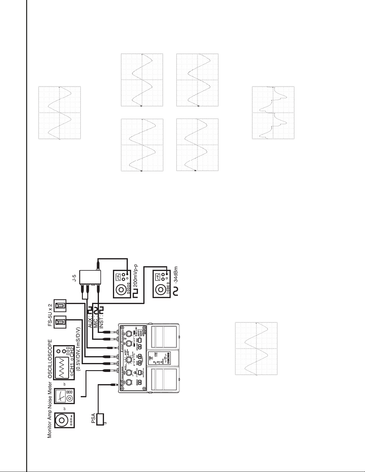
Items required for tests
• Oscillators x 2
• Oscilloscope
• Noise meter
• Monitor amp
• FS-5U x 2
• 1k ohm stereo short plug
• 150 ohm short plug
• 47k ohm short plug
• J-5
• Stereo mini <-> monaural phone conversion cable
Entering test mode
• Set all volumes to minimum.
• While holding down the left pedal (REC/PLAY/OVERDUB) and right
pedal (STOP/TAP TEMPO), connect the adaptor to the ADAPTOR
JACK to turn on the power.
• When only the POWER LED is lit, within two seconds press the left
pedal and then the right pedal.
• You will enter Test mode, and all LEDs other than "PEAK" will either
light or blink.
Note : A FLASH ROM check is automatically performed when
you enter Test mode. The state of the LEDs when you enter
Test mode will depend on the result of this test. For details
refer to the following item "1. FLASH check."
For details on how to skip directly to a desired test item,
refer to "Skipping directly to the desired test," following the
explanations of each test item.
Explanation of each test item
1. FLASH ROM check
• Enter Test mode.
• The FLASH ROM check will be performed when you enter Test mode.
• If there are no problems, all LEDs other than "PEAK" will light.
If there is a problem, the state of the LEDs will indicate the problem as
follows.
"OVERDUB" (yellow) blinking : MAKER ID error
"PLAY" (green) blinking : DEVICE ID error
"REC" (red) blinking : BUSY error
Note : If a problem was found, operation will stop and it will not
be possible to proceed to the next step. Turn off the power
to exit Test mode.
If there are any unlit LEDs regardless of whether or not
there was a problem, it is possible that the LED is faulty or
soldered incorrectly. (With the exception of "PEAK.")
2. Version number check
• Press the right pedal.
• The internal ROM version number and the external FLASH ROM ver-
sion number will be indicated by the LEDs.
Internal ROM version number display
This is indicated by the four LEDs "FLAT AMP SIMULATE", "CEN-
TER CANCEL", "NORMAL", and "INST & MIC."
"FLAT AMP SIMULATE" only lit : Ver1.00
"CENTER CANCEL" only lit : Ver1.01
"NORMAL" only lit : Ver1.02
"INST & MIC" only lit : Ver1.03
External FLASH ROM version number display
This is indicated by the following seven LEDs: "REVERSE", "TAP
TEMPO", "WRITE", "EXIT", "AUTO START", "MEMORY FULL",
and "LOOP QUANTIZE."
"REVERSE" only lit : Ver1.00
"TAP TEMPO" only lit : Ver1.01
"WRITE" only lit : Ver1.02
"EXIT" only lit : Ver1.03
"AUTO START" only lit : Ver1.04
"MEMORY FULL" only lit : Ver1.05
"LOOP QUANTIZE" only lit : Ver1.06
• After verifying the version, press the right pedal.
• All LEDs other than "PEAK" will light.
3. Switches and LED check
• Connect two FS-5U units to the PHRASE SHIFT jack and REVERSE
jack.
• Set the FS-5U polarity switches to the position shown in the diagram.
• Press the REVERSE switch.
• Verify that "REVERSE", "PLAY", "OVERDUB", and "PHRASE
USED" go dark, and that "TAP TEMPO" changes from orange to red.
• Press the TAP TEMPO switch, and verify that "TAP TEMPO" goes
dark.
• Press the WRITE switch, and verify that "WRITE" goes dark.
• Press the EXIT switch, and verify that goes dark "EXIT."
• Press the AUTO START switch, and verify that "AUTO START" goes
dark.
• Press the MODE switch, and verify that "INST & MIC", "NORMAL",
"CENTER CANCEL", and "FLAT AMP SIMULATE" go dark.
• Press the FS-5U that is connected to the PHRASE SHIFT jack, and ver-
ify that "MEMORY FULL" goes dark.
• Press the FS-5U that is connected to the REVERSE jack, and verify that
all LEDs other than "PEAK" light.
Page 2
RC-20 May. 2001
9
Excessive level NG Insufficient level NG
(0.5 V/DIV, 1 mS/DIV) (0.5 V/DIV, 1 mS/DIV)
+DC NG -DC NG
(0.5 V/DIV, 1 mS/DIV) (0.5 V/DIV, 1 mS/DIV)
6. DA check
• Once again check the output waveform at the point that "5. GUIDE vol-
ume check" is completed, to check the DC leakage and level.
In the following cases, the result is NG.
7. Output check
• Set the INST volume and MIC volume to 'maximum.'
• Set the PHRASE SELECT volume to the '2' position.
• Verify that "OVERDUB" and "REVERSE" are lit.
• Verify that the output waveform is as shown in the diagram.
Note : The waveform will change slightly depending on the inac-
curacy of the input function.
8. INST volume check
• Set the PHRASE SELECT volume to the '3' position.
• Verify that "REVERSE" is dark and "TAP TEMPO" is lit red.
(0.5 V/DIV, 1 mS/DIV)
200 Hz, 2.2 Vp-p ± 0.2 Vp-p
(0.5 V/DIV, 1 mS/DIV)
(0.5 V/DIV, 1 mS/DIV)
200 Hz, 2.2 Vp-p ± 0.2 Vp-p
gram below. Connect your oscilloscope to OUTPUT.
• Connect your waveform measurement equipment as shown in the dia-
4. LEVEL volume check
MIC : 200 Hz, sine wave, -34 dBm
AUX IN : 200 Hz, square wave, 200 mVp-p, STEREO
then back to the minimum position.
that the waveform increases smoothly.
At this time, the MODE LEDs will light consecutively from "FLAT
AMP SIMULATE," following the waveform.
• Move the LEVEL volume to approximately the center position, and
Input INST : 200Hz, square wave, 200 mVp-p
• Move the LEVEL volume from 'minimum' to 'maximum', and verify
is the same as shown in the diagram.
• With the LEVEL volume at maximum, verify that the output waveform
then back to the minimum.
that the waveform increases smoothly.
At this time, the MODE LEDs will change successively from "FLAT
AMP SIMULATE," following the waveform.
• Move the GUIDE volume to approximately the center position, and
• Move the GUIDE volume from 'minimum' to 'maximum,' and verify
5. GUIDE volume check
is the same as shown in the diagram.
• With the GUIDE volume at maximum, verify that the output waveform
Page 3
RC-20 May. 2001
10
(0.5 V/DIV, 1 mS/DIV)
1.2 Vp-p ± 0.2 Vp-p
(0.5V/DIV, 1mS/DIV)
(0.5V/DIV, 1mS/DIV)
• Set the INST volume to 'minimum,' and slowly move it to 'maximum.'
• Verify that the waveform increases smoothly.
• Verify that that when the INST volume is at maximum, the waveform is
the same as shown in the diagram.
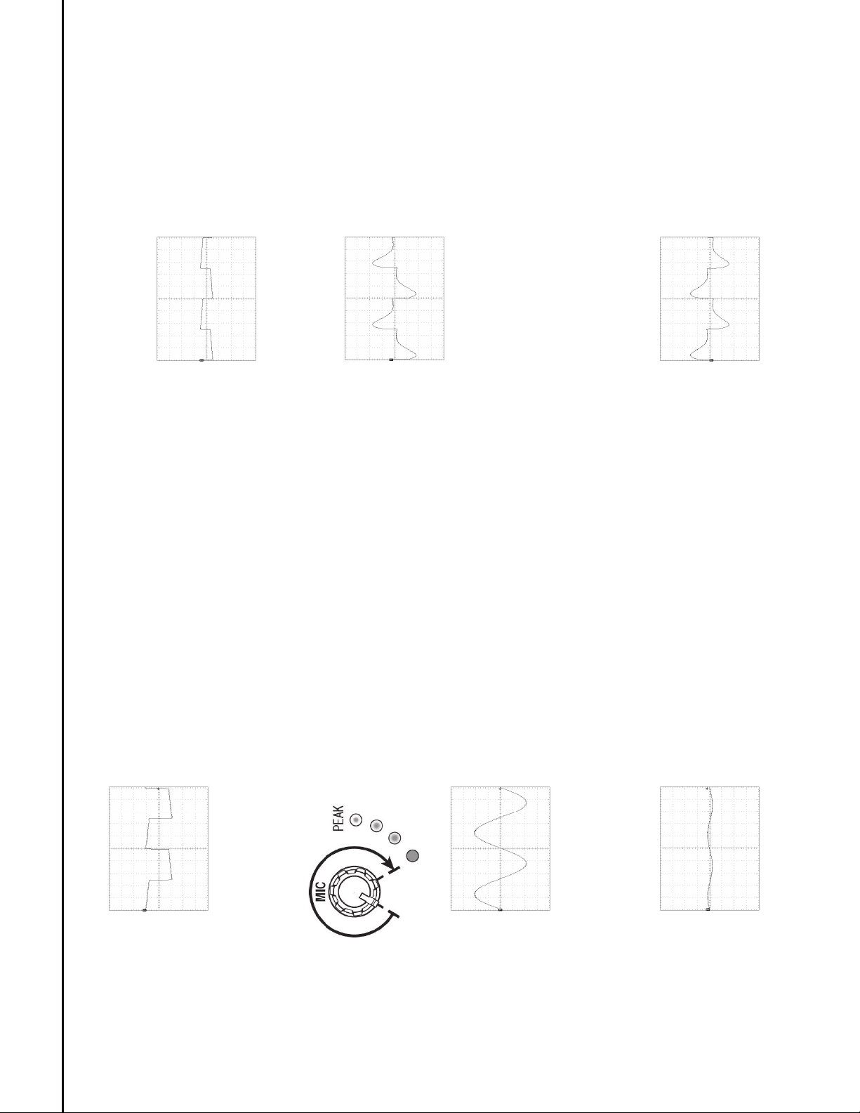
9. MIC volume check
• Set the PHRASE SELECT volume to the '4' position.
• Verify that "TAP TEMPO" changes from red to green.
• Set the MIC volume to minimum, and gradually move it to maximum.
• Verify that the waveform increases smoothly.
• Verify that "PEAK" lights as shown in the diagram.
• Verify that when MIC volume is at maximum, the waveform is the
same as shown in the diagram.
• Connect a noise meter to OUTPUT, and verify that the reading is in the
range of -1.0 dBm +/- 1.5 dBm.
10.MUTE check
• Set the PHRASE SELECT volume to the '5' position.
• Verify that "TAP TEMPO" is dark and "LOOP QUANTIZE" is lit.
• Verify that the output waveform is the same as the waveform shown in
the diagram.
• Connect a noise meter to OUTPUT, and verify that the reading is in the
range of -22.0 dBm +/- 1.5 dBm.
11.AUX IN (NORMAL) check
• Set the PHRASE SELECT volume to the '6' position.
• Verify that "LOOP QUANTIZE" is dark and "PHRASE USED" is lit.
• Verify that the output waveform is the same as the waveform shown in
the diagram.
12.AUX IN (FLAT AMP SIMULATE) check
• Set the PHRASE SELECT volume to the '7' position.
• Verify that "PHRASE USED" is dark and "INST & MIC" is lit.
• Verify that the output waveform is the same as the waveform shown in
the diagram.
• Press the FS-5U that is connected to the REVERSE jack, and verify that
the waveform does not decrease.
13.AUX IN (CENTER CANCEL) check
• Set the PHRASE SELECT volume to the '8' position.
• Verify that "INST & MIC" is dark and "NORMAL" is lit.
• Verify that there is no longer an output waveform.
Note : If the waveform remains, it is possible that the CENTER
CANCEL section is NG, or that there is a spot of solder on
the connector.
14.AUX IN (L ch) check
• Set the PHRASE SELECT volume to the '9' position.
• Verify that "NORMAL" is dark and "CENTER CANCEL" is lit.
• Input only the L channel to AUX IN.
• Verify that the output waveform is the same as the waveform shown in
the diagram.
Note : Verify that when compared with the output waveform of
"12. AUX IN (FLAT AMP SIMULATE) check," the phase
is inverted.
(0.5V/DIV, 1mS/DIV)
0.6Vp-p ± 0.1Vp-p
(0.5V/DIV, 1mS/DIV)
2.0Vp-p ± 0.2Vp-p
(0.5V/DIV, 1mS/DIV)
1.8Vp-p ± 0.2Vp-p
(The start illuminating of the LED indication.)
(The LED indication will stay illuminated.)
Page 4

RC-20 May. 2001
11
15.CN2 solder spot check
• Set the PHRASE SELECT volume to the '10' position.
• Verify that "CENTER CANCEL" is dark and "FLAT AMP SIMU-
LATE" is lit.
• Verify that there is no longer an output waveform.
Note : If the waveform remains, it is possible that there is a spot of
solder between pins 1-2 or 2-3 of CN2.
• Set the PHRASE SELECT volume to the '11' position.
• Verify that all LEDs are lit except for "PEAK."
• Verify that the output waveform is the same waveform as shown in the
diagram.
16.Noise check
• Set the PHRASE SELECT volume to the '2' position.
• Connect a 47k ohm short plug to the INST jack, a 150k ohm short plug
to the MIC jack, and a 1 k ohm stereo short plug to the AUX IN jack.
• Connect a monitor amp to OUTPUT.
• Set the INST volume and MIC volume to the maximum.
• Drop the unit from a height of 10 cm, and verify that no abnormal noise
is output.
• Turn the INST volume and MIC volume, and verify that no abnormal
noise is output.
• With the INST volume and MIC volume at the maximum positions,
measure the residual noise, and verify that it is less than -78 dBm (IHF-
A).
17.Battery operation check
• Put the battery in the battery compartment and insert the plug into the
INPUT jack.
• Check that power is turned on.
• Check that the unit is operating normally.
Note : Always check the battery after repairing or servic-
ing the product.
Skipping directly to the desired test
• Enter Test mode.
• The FLASH ROM check will occur automatically, and if there is no
problem, all LEDs other than "PEAK" will light.
• Follow the procedure described in the section for the test you want to
perform.
Note : In order to perform "5. GUIDE volume check," you must
first perform "4. LEVEL volume check."
Note : Even if it is not immediately after entering Test mode, you
can select the desired test item in the same way whenever all
LEDs other than "PEAK" are lit.
Exiting Test mode
• Disconnect the plug from the ADAPTOR jack to turn off the power.
Cautions
After repairing or servicing the product, you must check all test items.
SERIAL DUMP AND
UPDATE PROCEDURE
The following data can be transmitted and received between two RC-20
units without using any other devices.
1. Program
The operating program is stored in CPU ROM, but some processing can
be altered by applying patches.
This corresponds to such patch data.
2. Guide sound
3. Phrases (1 - 11)
Procedure
1. Connect the transmitting RC-20 and the receiving RC-20 as follows.
Connect the REVERSE jack and PHRASE SHIFT jack respectively.
Transmitting RC-20 Receiving RC-20
REVERSE ----------> PHRASE SHIFT
PHRASE SHIFT ----------> REVERSE
2. Start up the transmitting RC-20 in Dump mode.
1)While holding down the [TAP TEMPO] and [AUTO START] buttons,
turn on the power of the transmitting RC-20.
2)[EXIT] and the [FLAT AMP SIMULATE] and [REC] [PLAY]
[OVERDUB] indicators will light.
3. Start up the receiving RC-20 in Update mode.
1)Turn the [LEVEL] knob and [GUIDE] knob all the way to the left.
2)Set the [PHRASE SELECT] knob to 1.
3) While holding down the [REVERSE] and [MODE] buttons, turn on the
power of the receiving RC-20.
4)Within three seconds of turning on the power, press the [REVERSE]
button and then the [MODE] button.
[WRITE] and the [FLAT AMP SIMULATE] and [REC] [PLAY]
[OVERDUB] indicators will light.
* In Dump mode the [EXIT] indicator will light, but in Update mode the
[WRITE] indicator will light.
4. Select the data that you want to send from the transmitting RC-20
1)Press the [TAP TEMPO] button to select the data that you want to send.
[TAP TEMPO] indicator
Dark : Program, Guide sound, All phrases
Green : Specified phrase
Red : Guide sound
Orange : Program
2)If the [TAP TEMPO] indicator is green, use the [PHRASE SELECT]
knob to select the phrase that will be transmitted.
5. Transmit the data from the transmitting RC-20.
Transmission will begin when you press the left pedal of the transmit-
ting RC-20.
When the [MODE] indicators of both the transmitting RC-20 and the
receiving RC-20 stop at "FLAT AMP SIMULATE," transmission/
reception has been completed.
* With the factory settings, transmitting the program, guide sound, and all
phrases will require approximately 15 minutes.
Note : Never turn off the power until transmission/reception has
been completed.
(0.5V/DIV, 1mS/DIV)
200Hz, 2.2Vp-p ± 0.2Vp-p
Page 5

RC-20 May. 2001
12
State of the transmitting RC-20
"FLAT AMP SIMULATE" Waiting to transmit
* The RC-20 will briefly be in this state between data items.
* Since the guide sound data is divided into two parts, the RC-20 will
briefly be in this state even when transmitting only the guide sound
data.
"CENTER CANCEL" Now transmitting
"NORMAL" No data for transmission
State of the receiving RC-20
"FLAT AMP SIMULATE" Waiting for reception
* The RC-20 will briefly be in this state between data items.
* Since the guide sound data is divided into two parts, the RC-20 will
briefly be in this state even when receiving only the guide sound data.
"CENTER CANCEL" Now receiving
"NORMAL" Error
* An error will also occur if memory becomes full.
6. Repeat steps 4. -- 5. as necessary.
7. Turn off the power when you are finished.
Page 6

BOX
BATTERY
13
CN3CN4
+3.3V
DC/DC
CONVERTER
IC7
CN6
IC6B
IC5A IC6A
OUTPUT
REVERSE
CN2
SHIFT
PHRASE
FLAT AMP
IC2A
IC2B
FILTER
IC3A
AUX IN
IC3B
CENTER
CANCEL
FILTER
MIC
Q1
INST
JACK BOARD (75D433P001 2/2)
CN1
RC-20 Block Diagram
IC5
AD/DA
IC4
DRAM
CPU
IC1
IC2AIC2B
IC6
FLASH
MEMORY
IC3
GATE ARRAY
IC7
RESET IC
CN1
CENTER BOARD (75D433M000)
CN2 CN3
LED17
POWER LED
CN2 CN1
LED16
PEAK LED
VR
SW LED
VR5
MIC VR
CN3
VR4
INST VR
PANEL BOARD (75D433P001 1/2)
RC-20 May. 2001
BLOCK DIAGRAM
Page 7

RC-20 May. 2001
14
CIRCUIT BOARD (PANEL, JACK)
View from component side
Page 8

RC-20 May. 2001
15
CIRCUIT BOARD (PANEL, JACK)
View from foil side
Page 9

RC-20 May. 2001
16
CIRCUIT DIAGRAM (PANEL)
CENTER
CANCEL
PLAY
FLAT_AMP
SIM
(green)
REC
INST
GUIDE LEVEL
EXIT
WRITE
MODE
MIC
TAP
TEMPO
PEDAL_L
REVERSE
POWER
REVERSE
(red )
PEDAL_R
AUTO
START
PEAK
EXIT
OVER
DUB
LOOP
QUANTIZE
PHRASE
SELECT
AUTO
START
PHRASE
USED
NORMAL
INST
MIC
MEMORY
FULL
WRITETAP
TEMPO
TO CN2 ON
CENTER
BOARD
TO CN1 ON
JACK
BOARD
PEAK LED
POWER LED
MIC I N
MIC OUT
INST O UT
INST IN
75D433P000 1/2
*1: 0.47/16S = Submicron Chip Capacitor
*1
75D433P001 1/2
*1LOT-16LOT
*17LOT-
PANEL BOARD ASSY
AN11
AN10
AN12
+
D 3. 3
D
AVcc
A
AVcc
AA
AVcc
A
+
D 3. 3
D
AVcc
A
DA
C4
10/16
+
-
IC1A
M5218AF
2
3
1
R8
27k
R5 1M
+
-
IC1B
M5218AF
6
5
7
R6
1k
R7
1M
C5
10/16
D8
1SS352
SW6
SKQKAB
1 2
D4
1SS352
D1 1SS352
SW2
SKQKAB
1 2
SW1
SKQKAB
1 2
D2
1SS352
SW4
SKQKAB
1 2
VR2
RD901-40-125F-B54-11D (50KB 11clicks)
123
VR5
RD901-40-125F-AF5-00D (250KA)
1
2
3
LED4
L-312LRD
1 2
SW3
SKQKAH
1 2
D3 1SS352
SW5
SKQKAH
1 2
D5 1SS352
LED17
L-113GDT
12
VR4
RD901-40-125F-AF5-00D (250KA)
1
2
3
LED5
L-34HDSL
1 2
LED6
L-34HDSL
1 2
LED7
L-34HDSL
1 2
LED12
L-312LRD
1 2
LED11
L-34HDSL
1 2
LED3
L-34HDSL
1 2
VR1
RD901-40-125F-B54-00D (50KB)
123
C6
10/16
D7 1SS352
VR3
RD901-40-125F-B54-00D (50KB)
123
LED16
L-34HDSL
1 2
R1
1.2k
LED15
L-312LRD
1 2
LED8
L-34HDSL
1 2
LED1
L-34YDSL
1 2
LED9
GL3ED8
1 2
3
LED2
L-34GDSL
1 2
LED10
L-34GDSL
1 2
LED14
L-312LRD
1 2
LED13
L-34HDSL
1 2
R4
330
C9
10/16
R9
47k
C8
10/16
R10
47k
D9
02DZ5.1-Y
1 2
+
-
IC1C
M5218AF
84
Q2
2SC4116GR
1
2 3
R2
10k
R3
100k
Q1
2SC4116GR
1
2 3
C2
1/50
C1
1/50
CN1
WIRING 10P
11223344556677889910
10
CN2
WIRING 11P
112233445566778899101011
11
C3
0.1
D10
N.I.U.
1 2
C10
0.47/16S
C7
10/16
CN3
WIRING 8P
112233445566778
8
SW7
SKQKAB
1 2
D6
1SS352
SW8
SKQKAB
1 2
Page 10

RC-20 May. 2001
17
CIRCUIT DIAGRAM (JACK 1-16 LOT)
INST
MIC
AUX_IN
*1: 0.47/16S = Submicron Chip Capacitor
REVERSE
PHASE
SHIFT
TO CN1 ON
CENTER BOARD
OUTPUT
INST OUT
INST IN
TO CN3 ON
PANEL BOARD
POWER LED
PEAK LED
MIC IN
MIC OUT
INST OUT
INST IN
*1
*2
*4 *4
MIC IN
MIC OUT
0 ohm(3216 Type):2 LOT - 16 LOT
*2: No Mounting
*3: Jamper Wire:1 LOT
*4: 0 ohm(1608 Type):1 LOT - 16 LOT
or HSJ0857-01-1210
*1
*1
*1
*1
*3
*2
*2
*2
75D433P000 2/2
JACK BOARD ASSY
DA_R
DA_L
FET SW
FLAT_AMP_ON/OFF
REVERSE
AUX_C.CANCEL_MUTE
MIC_MUTE
T_SHIFT
AUX_NORM_MUTE
INST_MUTE
A
1/2AVcc
1/2AVcc
A
A
AVcc
1/2AVcc
A
1/2AVcc
AVcc
A
A
AVcc
AVcc
A
1/2AVcc
A
A
A
A
AVcc
A
A
A
AVcc
A
1/2AVcc
D
D
D
D
D
+
D 3. 3
D
AVcc
+
D 3. 3
1/2AVcc
A
A
AVcc
A
AVcc
A
AVcc
AVcc
AVcc
A
AVcc
A
AVcc
A
A
+
D 3. 3
D
D
+
D 3. 3
1/2AVcc
D
1/2AVcc
AVcc
A
D
1/2AVcc
A
A
A
D
D
A
A
AVcc
A
AVcc
AVcc
R1
10k
R2
1M
JK3
AJ324A-3C
123
R28
47K
R23
22K
R26
22K
R29
47K
R24
47K
L1
N2012Z601T2
L6
N2012Z601T2
R12
10k
R47
100k
C24
10/16
R46
1k
C5
1/50
JK7
HTJ-064-12D
123
C21
NFM4516P13C204F
C23
100/16
C26
47/6.3
R48
10k
+
-
IC6B
M5218AF
6
5
7
R33
15k
C20
N.I.U
R34
56k
R37
47k
+
-
IC5A
M5218AF
2
3
1
R39
47k
R41
56k
C13
N.I.U
R11
10k
C3
0
L3
N2012Z601T2
+
-
IC2C
M5218AF
84
+
-
IC6C
M5218AF
84
IC1E
TC4066BFT
14
7
C10
0.47/16S
+
-
IC3B
M5218AF
6
5
7
+
-
IC5B
M5218AF
6
5
7
R27
10K
C1
0.47/16S
R36
68k
C25
0
Q9
N.I.U
1
2 3
R45
0
Q8
N.I.U
1
32
D6
N.I.U
12
R43
N.I.U
D5
N.I.U
12
C27
N.I.U
D4
N.I.U
1 2
R44
N.I.U
R49
N.I.U
R15
10k
Q2
2SC4116GR
1
2 3
C8
0.01
R13
100k
R8
4.7k
C6
0.027
L8
N2012Z601T2
L10
N2012Z601T2
C17
100P
CN4
RIBON 3P
11223
3
CN3
RIBON 3P
11223
3
IC7
S-8520E33MC-BJS
ON/OFF1VIN5VSS
2
EXT
4
VOUT
3
C29
100/16
C28
0.1
L15
SLF7032T-4R7M1R7-2 4.7uH
C19
10p
L16
SLF7032T-151MR37-2 150uH
R40
39k
+
-
IC6A
M5218AF
2
3
1
R35
56k
C14
0.0056
R31
12K
R38
56k
CN6
53015-0210
112
2
IC1D
TC4066BFT
11 10
12
IC1C
TC4066BFT
8 9
6
IC4B
TC4W66F
5 6
3
DA1
1SS302
21
3
DA2
1SS302
21
3
DA4
1SS302
21
3
DA5
1SS302
21
3
DA6
1SS302
21
3
+
-
IC5C
M5218AF
84
Q1
2SK880GR
3
1 2
L13
N2012Z601T2
L2
N2012Z601T2
L9
N2012Z601T2
L12
N2012Z601T2
L7
N2012Z601T2
L14
SBT-0460TF
R6
100k
C4
0.01
JK1
HTJ-064-12I
241
JK2
HTJ-064-12I
241
JK6
DJ-0711-020
312
JK4
HTJ-064-12I
241
Q10
IRF7606
D
7
G
4
D
5
S
2
D
6
S3S
1
D
8
D7
SS14
1 2
D3
SS14
1 2
+
-
IC3A
M5218AF
2
3
1
C30
470p
C31
470p
CN2
WIRING 14P
112233445566778899101011111212131314
14
C18
1/50
C12
100P
IC1B
TC4066BFT
4 3
5
+
-
IC2A
M5218AF
2
3
1
+
-
IC2B
M5218AF
6
5
7
R19
47k
R9
47k
Q6
RN1307
1
2 3
R16
47k
C7 100p
R17
47k
R18
47k
R14
100k
Q7
RN1307
1
2 3
R5 47k
IC1A
TC4066BFT
1 2
13
Q4
RN1307
1
2 3
Q3
RN1307
1
2 3
C2
1/50
R4
47k
Q5
RN1307
1
2 3
R10
47k
R20
47k
R50
10k
FL1
SBT-0180W
1
2
4
3
IC4A
TC4W66F
1 2
7
R25
47K
R30
47K
C11
0.1
R7
82k
Q11
2SK880GR
3
1 2
D9
1SS355
1 2
R51
1M
Q12
RN1307
1
2 3
R53
47k
JK5
HTJ-064-12I
241
R52
4.7k
R3
10k
CN1
A2001WR2-8P
112233445566778
8
+
-
IC3C
M5218AF
84
C33
10p
R55
47k
R21
10K
DA3
1SS302
21
3
R22
47K
C9
0.47/16S
L5
N2012Z601T2
R54
22k
C34
0.47/16S
R57
47k
R56
22k
C35
0.47/16S
C36
100p
C37
100p
R58
15k
C39
1/50
R42
10k
C22
N.I.U
IC4C
TC4W66F
8
4
C32
0.01
D11
1SS352
12
D12
1SS352
12
C40
100/16
C38
0.1
L4
N2012Z601T2
Page 11

RC-20 May. 2001
18
CIRCUIT DIAGRAM (JACK 17 LOT up)
INST
MIC
AUX_IN
*1: 0.47/16S = Submicron Chip Capacitor
REVERSE
PHASE
SHIFT
TO CN1 ON
CENTER BOARD
OUTPUT
INST OUT
INST IN
TO CN3 ON
PANEL BOARD
POWER LED
PEAK LED
MIC IN
MIC OUT
INST OUT
INST IN
*2
*2
MIC IN
MIC OUT
*2: No Mounting
or HSJ0857-01-1210
*1
*1
*1
75D433P001 2/2
JACK BOARD ASSY
DA_R
DA_L
FET SW
FLAT_AMP_ON/OFF
AUX_C.CANCEL_MUTE
MIC_MUTE
T_SHIFT
AUX_NORM_MUTE
INST_MUTE
REVERSE
A
1/2AVcc
1/2AVcc
A
A
AVcc
1/2AVcc
A
1/2AVcc
AVcc
A
A
AVcc
AVcc
A
1/2AVcc
A
A
A
A
AVcc
A
1/2AVcc
D
D
D
D
D
+
D 3. 3
D
AVcc
+
D 3. 3
1/2AVcc
A
A
AVcc
A
AVcc
A
AVcc
AVcc
AVcc
A
AVcc
A
AVcc
A
A
+
D 3. 3
D
D
+
D 3. 3
1/2AVcc
D
1/2AVcc
AVcc
A
D
1/2AVcc
A
A
A
D
D
A
A
AVcc
A
AVcc
AVcc
+
D 3. 3
+
D 3. 3
R1
10k
R2
1M
JK3
AJ324A-3C
123
R28
47K
R23
22K
R26
22K
R29
47K
R24
47K
L1
N2012Z601T2
L6
N2012Z601T2
R12
10k
R47
100k
C24
10/16
R46
1k
C5
1/50
JK7
HTJ-064-12D
123
C21
NFM4516P13C204F
C23
100/16
C26
47/6.3
R48
10k
+
-
IC6B
M5218AF
6
5
7
R33
15k
C20
N.I.U
R34
56k
R37
47k
+
-
IC5A
M5218AF
2
3
1
R39
47k
R41
56k
C13
N.I.U
R11
10k
L3
N2012Z601T2
+
-
IC2C
M5218AF
84
+
-
IC6C
M5218AF
84
IC1E
TC4066BFT
14
7
C10
0.47/16S
+
-
IC3B
M5218AF
6
5
7
+
-
IC5B
M5218AF
6
5
7
R27
10K
C1
0.47/16S
R36
68k
R15
10k
Q2
2SC4116GR
1
2 3
C8
0.01
R13
100k
R8
4.7k
C6
0.027
L8
N2012Z601T2
L10
N2012Z601T2
C17
100P
CN4
RIBON 3P
11223
3
CN3
RIBON 3P
11223
3
IC7
S-8520E33MC-BJS
ON/OFF1VIN5VSS
2
EXT
4
VOUT
3
C29
100/16
C28
0.1
L15
SLF7032T-4R7M1R7-2 4.7uH
C19
10p
L16
SLF7032T-151MR37-2 150uH
R40
39k
+
-
IC6A
M5218AF
2
3
1
R35
56k
C14
0.0056
R31
12K
R38
56k
CN6
53015-0210
112
2
IC1D
TC4066BFT
11 10
12
IC1C
TC4066BFT
8 9
6
IC4B
TC4W66F
5 6
3
DA1
1SS302
21
3
DA2
1SS302
21
3
DA4
1SS302
21
3
DA5
1SS302
21
3
DA6
1SS302
21
3
+
-
IC5C
M5218AF
84
Q1
2SK880GR
3
1 2
L13
N2012Z601T2
L2
N2012Z601T2
L9
N2012Z601T2
L12
N2012Z601T2
L7
N2012Z601T2
L14
SBT-0460TF
R6
100k
C4
0.01
JK1
HTJ-064-12I
241
JK2
HTJ-064-12I
241
JK6
DJ-0711-020
312
JK4
HTJ-064-12I
241
Q10
IRF7606
D
7
G
4
D
5
S
2
D
6
S3S
1
D
8
D7
SS14
1 2
D3
SS14
1 2
+
-
IC3A
M5218AF
2
3
1
C30
470p
C31
470p
CN2
WIRING 14P
112233445566778899101011111212131314
14
C18
1/50
IC1B
TC4066BFT
4 3
5
+
-
IC2A
M5218AF
2
3
1
+
-
IC2B
M5218AF
6
5
7
R19
47k
R9
47k
Q6
RN1307
1
2 3
R16
47k
C7 100p
R17
47k
R18
47k
R14
100k
Q7
RN1307
1
2 3
R5 47k
IC1A
TC4066BFT
1 2
13
Q4
RN1307
1
2 3
Q3
RN1307
1
2 3
C2
1/50
R4
47k
Q5
RN1307
1
2 3
R10
47k
R20
47k
R50
10k
FL1
SBT-0180W
1
2
4
3
IC4A
TC4W66F
1 2
7
R25
47K
R30
47K
C11
0.1
R7
82k
Q11
2SK880GR
3
1 2
D9
1SS355
1 2
R51
1M
Q12
RN1307
1
2 3
R53
47k
JK5
HTJ-064-12I
241
R52
4.7k
R3
10k
CN1
A2001WR2-8P
112233445566778
8
+
-
IC3C
M5218AF
84
C33
10p
R55
47k
R21
10K
DA3
1SS302
21
3
R22
47K
C9
0.47/16S
L5
N2012Z601T2
R54
22k
C34
10/16
R57
47k
R56
22k
C35
10/16
C36
100p
C37
100p
R58
15k
C39
1/50
R42
10k
IC4C
TC4W66F
8
4
C32
0.01
D11
1SS352
12
D12
1SS352
12
C40
100/16
C38
0.1
L4
N2012Z601T2
R60
1K
R62
1K
R61
470k
C12
100P
R59
470k
+
-
+
-
Page 12

RC-20 May. 2001
19
CIRCUIT BOARD (CENTER)
View from component side View from foil side
Page 13

RC-20 May. 2001
20
CIRCUIT DIAGRAM (CENTER)
(fc=32k)
TO CN2 ON
JACK BOARD
TO CN2 ON
PANEL
BOARD
TO CN1 ON
PANEL
BOARD
AUX_C.CANCEL_MUTE
FLAT_AMP_ON/OFF
AUX_NORM_MUTE
INST_MUTE
MIC_MUTE
CENTER BOARD ASSY
75D433M000
XLWR
XRD
A9
CD_RE
DMARQ1
A6
CD4
DMARQ0
CD_RB
A9A4A4
CD3
CD_ALE
CD1
CD5
DMARQ0
CD_RE
CD_WP
CD_CLE
CD_ALE
A3
A7
A7A5A4
CD4
A1
CD8A2CD7
CD1
A6
CD_RB
CD3
A5A2A3
A1
A9
A8
CD2
CD6
A1
A6
A3
CD2
CD7
A2
CD_WE
A5
A8
A7
A8
CD_CLE
CD_WE
DMARQ1
CD6
CD5 CD8
D6
D14
D15
D12
D2
D1D3D3D0
D13D7D7
D13
D5
D2
D11
D14
D0D4D4
D11
D12D5D6
D15
D1
D0
D1D2D3D4D5D6D7
D11
D12
D13
D14
D15
CD_CE
CD_CE
DA_L
D10
D9
D9
D8
D10D9D8 D10
D8
T_SHIFT_INC
FET SW
FET SW
T_SHIFT_INC
DA_R
CD_SW
CD_PRTCT
CD_WP
DMAAK0
DMAAK1
DMAAK0
DMAAK1
P104
P104
T_SHIFT
P107
REVERSE
REVERSE
P105
REVERSE
P106
P106
P107
P105
P103
P103
FET SW
+
D 3. 3
+
D 3. 3
D
D
D
D
+
D 3. 3
D
D
+
D 3. 3
+
D 3. 3
D
D
+
D 3. 3
D
D
D
D
D
D
A
+
D 3. 3
D
+
D 3. 3
+
D 3. 3
D
D
A
A
D
+
D 3. 3
+
D 3. 3
A
A
+
D 3. 3
D
D
D
D
D
+
D 3. 3
D
+
D 3. 3
+
D 3. 3
D
+
D 3. 3
D
+
D 3. 3
+
D 3. 3
D
D
+
D 3. 3
D
+
D 3. 3
A
X3
AT-41CD2 (6.4MHz)
1 2
C42
100/6.3
C4 100/6.3C3100/6.3
C22
0.1
C23
0.1
CN4
N.I.U.
1122334455667
7
C16
0.1
C39
10p
C14
0.1C90.1
C1
100/6.3
C5
0.1
C11
0.1
C28
10/16
C12
0.1C60.1
C10
0.1
C32
10/16
IC5
AK4552VT
LIN
2
SDTO
8
RIN
1
VD
5
MCLK
11
BCLK
12
PDN
13
DEM1
7
VCOM
14
LRCK
10
VSS
3
SDTI
9
DEM0
6
VA
4
ROUT
16
LOUT
15
R19
1M
D1
1SS352
12
C34 47p
C35 47p
R20
15
C13
0.0056
R4
56k
R1
12k
R2
15k
C17
N.I.U
R3
10k
R5
10k
+
-
IC2B
NJM2100M
6
5
7
C20
10/16
+
-
IC2A
NJM2100M
2
3
1
R11
10k
R12
10k
C210/16
IC4 LC32V4265T-25
VCC
6
I/O12I/O23I/O34I/O4
5
VCC
22
I/O57I/O68I/O79I/O8
10
NC13NC
14
WE15RAS
16
NC17A018A119A220A321A424A525A626A727A8
28
OE29UCAS30LCAS
31
NC
32
I/O9
35
I/O1036I/O1137I/O12
38
VSS
23
I/O1340I/O1441I/O1542I/O16
43
VSS44VSS
39
VCC
1
L2
N2012Z601T2
L3
N2012Z601T2
L1N2012Z601T2
R23
100
L6 N2012Z601T2
C30
10/16
C44 0.0056
S-80930ALMP-DAT-T2
IC7
NC
4
Cp
5
VDD2VSS
3
OUT
1
IC6
TC58V64AFT
NC39NC38NC37NC
36
NC
35
GND
40
NC32NC31NC30NC29NC
28
I/O827I/O726I/O625I/O5
24
RE42R/B41WP5WE
4
NC15NC14NC13NC
17
I/O421I/O320I/O219I/O1
18
NC
10
Vss
1
CLE2ALE
3
NC6NC7NC8NC9NC
16
Vss
22
Vccq
23
CE
43
Vcc
44
X1
N.I.U.
12
L4
N2012Z601T2
L7
N2012Z601T2
L5
N2012Z601T2
IC3
LC24085B-SD1
LCD_DATA166LCD_DATA0
67
LCD_POWER_U/D
59
LCD_DATA562LCD_DATA463LCD_DATA265LCD_DATA3
64
EXTAL
93
XP_CLK
56
SPRX_LRCK44SPRX_BCK
45
PRESET_CTRL
58
VDD
18
VDD
37
WCK_IN
43
VSS
1
VSS
19
VSS
36
VSS
55
CPU_WR27CPU_RD28CPU_CS29XP_CS_IN
30
PLL_LOCK38S139S240PLL_SEND
41
WAIT_CA
47
AR_SYNC_WCK42XP_WCK
50
XTAL
92
LCD_DATA661LCD_DATA7
60
LCD_E
68
LCD_R/W
69
LCD_RS
70
ENC_A
110
ENC_B
111
7SEG_COM0
112
7SEG_COM1
113
7SEG_COM2
114
7SEG_COM3
115
7SEG_COM4
105
7SEG_DATA7
123
7SEG_DATA6
122
7SEG_DATA5
121
7SEG_DATA4
120
7SEG_DATA3
119
7SEG_DATA2
118
7SEG_DATA1
117
7SEG_DATA0
116
TEST
97
LRCK
104
BCK
103
MCK
102
DAOUT1
101
ADIN1
100
DAOUT0
99
ADIN0
98
DATA886DATA694DATA595DATA489DATA788DATA285DATA184DATA3
87
SW
96
PROTECT
76
WE
81
CE78RE
80
ALE
79
WP
83
A926A8
25
D77D66D55D44D3
142D2141D1140D0139
A724A623A522A421A320A217A1
16
A19
131
A18
130
D1515D1414D1313D1212D1111D1010D99D8
8
PHAI
32
RESET
33
SPRX_SD
46
WAIT_CB
48
XP_SCK51XP_LRCLK49XP_SD52XP_WR
53
VDD
54
VSS
72
VDD
73
CLE
77
VDD
90
VSS
91
VSS
108
VDD
126
VSS
127
XCD_POWER
129
XCS
128
WAIT_OUT
125
CPU_TIMER
124
DMA_REQ0
132
DMA_REQ1
133
DMA_REQ2
134
DMA_ACK0
135
DMA_ACK1
136
DMA_ACK2
137
INT_OUT
138
VDD
144
VDD
109
NC2NC3NC34NC35NC71NC74NC75NC
106NC107NC143
SM_CS_IN
31
R/B
82
PLL_RETURN
57
RA1CRN34680J
1 8
2 7
3 6
4 5
RA3CRN34680J
1 8
2 7
3 6
4 5
RA4CRN34680J
1 8
2 7
3 6
4 5
RA5CRN34680J
1 8
2 7
3 6
4 5
RA7
CRN34103J
1 8
2 7
3 6
4 5
RA12 CRN34680J
1 8
2 7
3 6
4 5
C15
10p
C18
100/16
C19
0.1
X2
MA-406 (24.576MHz)
14
RA11
CRN34680J
1 8
2 7
3 6
4 5
R13
68
RA6 CRN34680J
1 8
2 7
3 6
4 5
RA8 CRN34680J
1 8
2 7
3 6
4 5
C260.1
C270.1
C250.1
RA2
CRN34103J
1 8
2 7
3 6
4 5
CN2
A2001WR2-11P
11223344556677889
9
101011
11
R6 220 R7 100
R9 100
R10
100
R14 220
R15 100
R17 100 R18 100
CN3
A2001WR2-10P
11223344556677889910
10
R22 100
RA10
CRN34680J
1 8
2 7
3 6
4 5
RA9
CRN34680J
1 8
2 7
3 6
4 5
R8 68
TP1 TP
1
IC1
UPD703102GJ-33
DMARQ04DMARQ13DMARQ22TO100/P008TO101/P017P035P02
6
AVREF
36
AVDD
34
AVSS
35
VDD
45
CVDD
62
INTP103
1
RESET
71
HVDD
100
HVDD
126
VDD
144
VSS
9
VSS
83
VSS
117
VSS
135
WR
88RD89
UWR
90
LWR
91
CS792CS693CS594CS495CS396CS297CS1
98
RAS0
99
MODE370MODE269MODE168MODE0
67
CVSS
65
CKSEL
66
X263X1
64
P17 / INTP11310P16 / INTP11211P15 / INTP11112P14 / INTP11013P1314P1215P1116P1017P10718P10619P10520P10421P10322P10223P10124P10025ANI726ANI627ANI528ANI429ANI330ANI231ANI132ANI033P20/NMI37P2138SO039SI040SCK041TXD142RXD143P2744P3746P3647P3548P3449P3350TCLR13/P3251TO131/P3152TO130/P3053P11754P11655P11556P11457P11358P11259P11160P11061P12772P12673P12574P12475P12376P12277P12178P12079CLKOUT/PX780PX6/WAIT81PX582P9784P9685P9586P94
87
A15
109
A14
110
A13
111
A12
112
A11
113
A10
114
A9
115A8116
D7
136D6137D5138D4139D3140D2141D1142D0143
A7
118A6119A5120A4121A3122A2123A1124A0125
A23
101
A22
102
A21
103
A20
104
A19
105
A18
106
A17
107
A16
108
D15
127
D14
128
D13
129
D12
130
D11
131
D10
132
D9
133D8134
R24
1.5k
Q2
RN1307
1
23
Q3
RN2307
1
32
C37
0.1
C40
10p
R21
10K
C41
0.1
C8 0.1
C21
0.1
C31
0.1
C36
0.1
C70.1
C43
0.1
C38
0.1
C24
100/6.3
Q1
RN1307
1
23
Q5
RN2307
1
32
Q6
RN2307
1
32
Q7
RN2307
1
32
Q8
RN2307
1
32
Q9
RN2307
1
32
Q10
RN2307
1
32
Q4
RN2307
1
32
R25
N.I.U.
C45
N.I.U.
C46
100/6.3
R26
47
IC8
TC7S08F
1
2
4
53
C47
0.1
TP3
TP
1
R27
10k
R28
10k
TP2 TP
1
R29
10k
TP17 TP
1
TP4 TP1TP5 TP1TP6 TP1TP7 TP1TP8 TP1TP9 TP1TP10 TP1TP11 TP1TP12 TP1TP16 TP1TP13 TP1TP14 TP1TP15 TP
1
TP18 TP
1
CN1
A2001WR2-14P
112233445566778899101011111212131314
14
R30 100
R16
10
C33
0.1
C29
0.1
+
-
IC2C
NJM2100M
84
+3.3V
+3.3V
 Loading...