

Page 1
Dec.2004
TABLE OF CONTENTS
CAUTIONARY NOTES........................................................ 2
SPECIFICATIONS................................................................. 2
LOCATION OF CONTROLS............................................... 3
LOCATION OF CONTROLS PARTS LIST ....................... 3
EXPLODED VIEW 1 ............................................................. 4
EXPLODED VIEW 1 PARTS LIST ...................................... 4
EXPLODED VIEW 2 ............................................................. 5
EXPLODED VIEW 2 PARTS LIST ...................................... 5
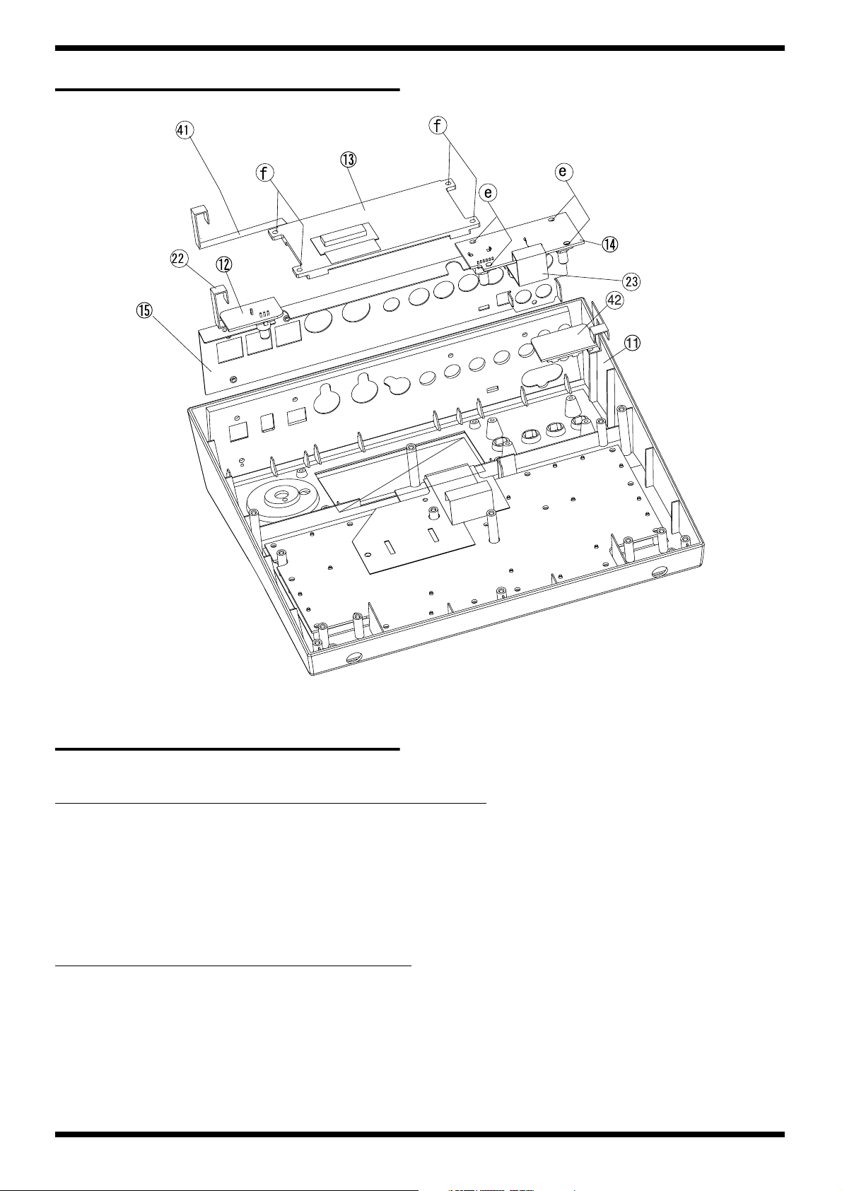
EXPLODED VIEW 3 ............................................................. 6
EXPLODED VIEW 3 PARTS LIST ...................................... 6
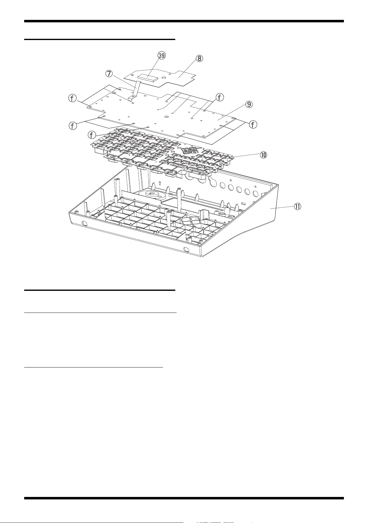
EXPLODED VIEW 4 ............................................................. 7
EXPLODED VIEW 4 PARTS LIST ...................................... 7
TAPE for fixed wring............................................................ 8
LOCATION TO PASTE of FOOT (Inside of Bottom) ...... 9
WIRING DIAGRAM........................................................... 10
WIRING DIAGRAM PARTS LIST.................................... 10
PARTS LIST.......................................................................... 12
DR-880
SERVICE NOTES
Issued by RJA
CHECKING THE VERSION NUMBER ...........................16
Computer to DR-880 connection .......................................16
USERS DATA SAVE AND LOAD ....................................16
FACTORY RESET INSTRUCTIONS ................................. 17
SYSTEM SOFTWARE UPDATING INSTRUCTIONS.... 18
TEST MODE.......................................................................... 18
BLOCK DIAGRAM .............................................................28
CIRCUIT BOARD (MAIN BOARD).................................. 30
CIRCUIT BOARD (MAIN BOARD).................................. 32
CIRCUIT DIAGRAM (MAIN, VOLUME)........................ 34
CIRCUIT DIAGRAM (JACK).............................................36
CIRCUIT DIAGRAM (POWER) ........................................38
CIRCUIT BOARD (SW)....................................................... 40
CIRCUIT BOARD (SW)....................................................... 42
CIRCUIT DIAGRAM (SW, ENCODER, PIN, INPUT,
PHONES) ..............................................................................44
ERROR MESSAGES............................................................. 46
Copyright © 2004 ROLAND CORPORATION
All rights reserved. No part of this publication may be reproduced in any form without the written permission
of ROLAND CORPORATION.
Printed in Japan (0500) (AS)17058298E0
Page 2

Dec.2004
CAUTIONARY NOTES
User data status
User data status after each of the following processes is described below.
Whenever carrying out procedures that involve deleting or erasing user data,
always be sure to back up the user data to some form of external media (refer
to Saving and Loading Data).
Process User Data
Checking Version number Preserved
Factory Reset Deleted
System Update Preserved
Test Mode Preserved
* Executing Test Mode during Factory Reset deletes the user data.
PARTS LIST
Due to one or more of the following reasons, parts with parts code ********
cannot be supplied as service parts.
• Part supplied only as a component in a complete assembly
• Copyright does not permit the part to be supplied
• Part is sold commercially
Resolution
Per quarter note: 96
Tempo
Quarter note: 20-260 bpm
Pads
20 with velocity sensitive
Display
Custom LCD with backlight
Connectors
(Rear)
Master Out L (MONO), R (1/4” Phone Type)
Master Out L, R (Phono Type)
Individual A, B (1/4” Phone Type)
Digital Out (coaxial)
CTL 1,2 (TRS 1/4” Phone Type)
CTL 3,4/EXP PEDAL (TRS 1/4” Phone Type)
USB
MIDI IN, OUT
AC Adaptor
(Front)
Phones (Stereo 1/4” Phone Type)
Guitar/Bass Input (1/4” Phone Type)
CIRCUIT BOARD
NIU meant that "NOT IN USE " there don't set any contents in the Circuit
Diagram.
There has silk-screen only in the Circuit Board.
SPECIFICATIONS
Specifications
DR-880: Dr.Rhythm
Maximum Polyphony
32 voices
* Depending on the bass tone used, maximum polyphony may be lower.
Instruments
Drum: 440
Bass: 40
Kits
Preset: 100
User: 100
Patterns
Preset: 500
User: 500
Songs
User: 100
Power Supply
AC Adaptor (BRC series)
Power Consumption
600 mA (Max.)
Dimensions
273 (W) x 242 (D) x 72 (H) mm
10-3/4 (W) x 9-9/16 (D) x 2-7/8 (H) inches
Weight
1.4 kg / 3 lbs 2 oz (excluding AC adaptor)
Accessories
AC Adaptor 100V (#G2457143)
120V (#G2457144)
230V (#G245714101)
240V (#G2457142)
Owner’s Manual English (#G6017380)
Japanese (#G6017379)
DR-880 Driver CD-ROM (#G2567133)
Roland Service (Information sheet) (#********)
Options
Foot Switch (FS-5U)
Dual Foot Switch (FS-6)
Expression Pedal (Roland EV-5)
Foot Switch Cable (Roland PCS-31)
(stereo 1/4” phone plug-1/4” phone plug x 2)
* In the interest of product improvement, the specifications and/or appearance of
this unit are subject to change without prior notice.
Maximum Note Storage
Approx. 30,000 notes
* This may be smaller than this depending on the contents of created pattern and
song.
2
Page 3
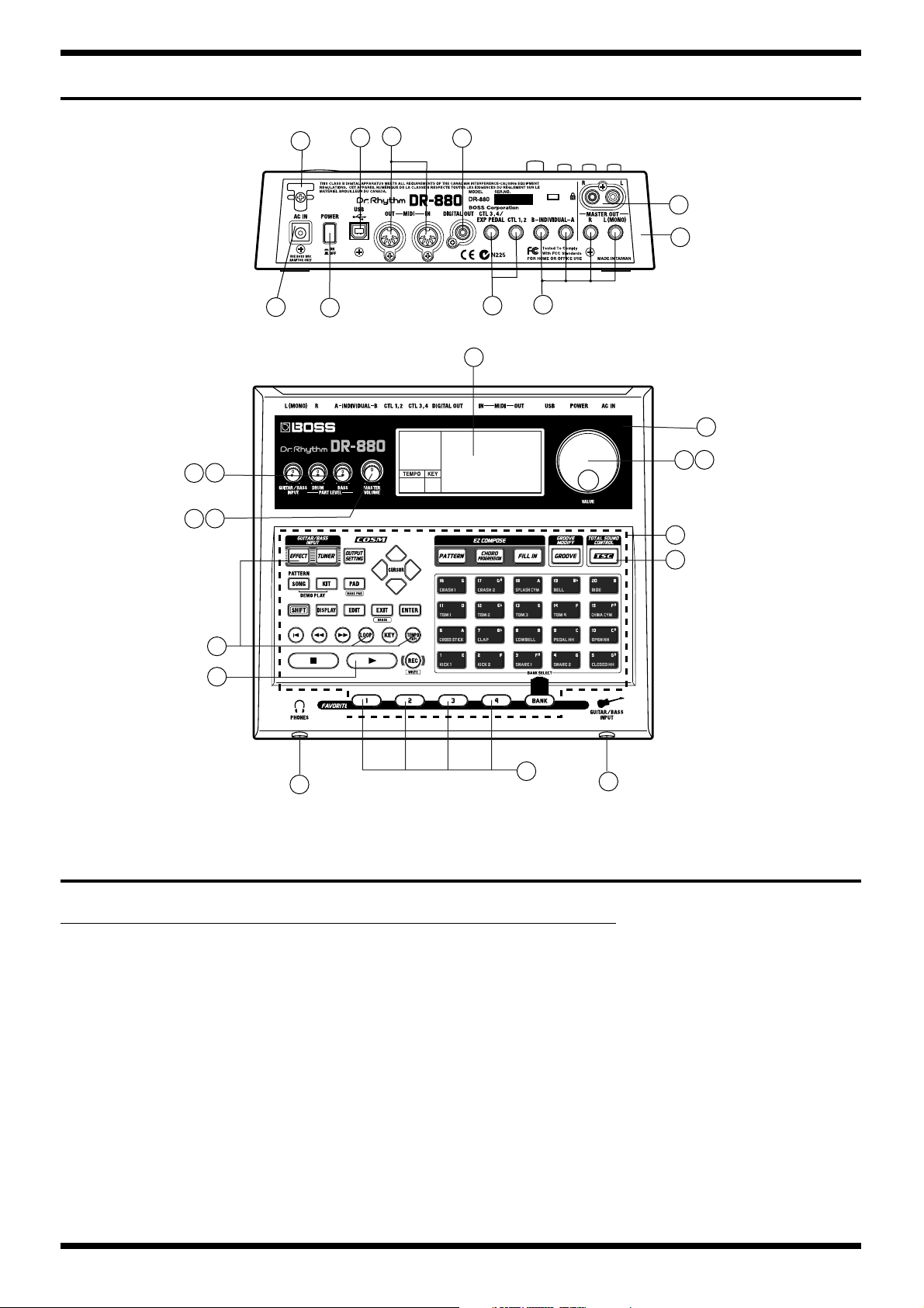
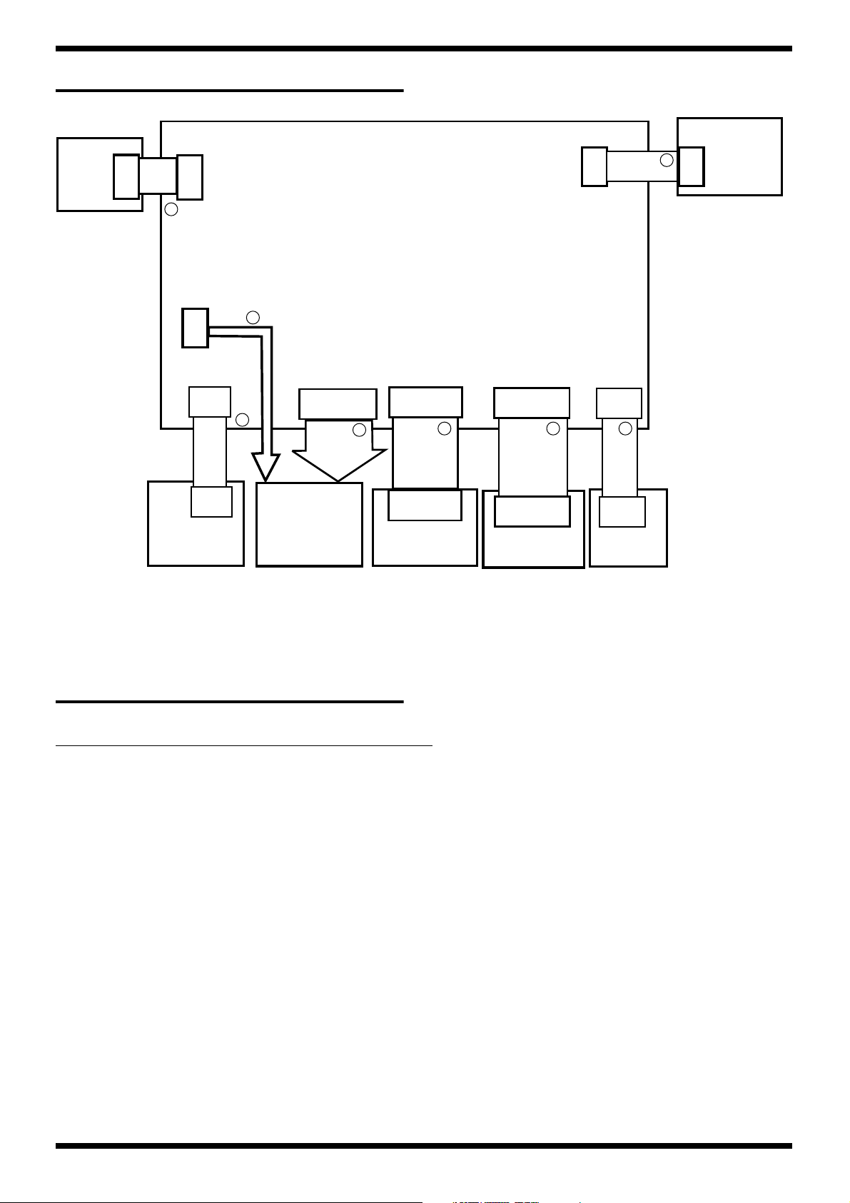
LOCATION OF CONTROLS
fig.DR-880-Panel.eps
5
28
29
DR-880
30
33
11
27
6
31
32
13
4
38
3
36
2
37
1
10
34
34
35
31
34
LOCATION OF CONTROLS PARTS LIST
No. PART CODE CATEGORY PART NAME DESCRIPTION Q'TY
1 F2477101 KNOB,BUTTON DR-KNOB 1
2 22480260 KNOB,BUTTON P R-KNOB MF BLK/LCG 1
3 01340412 KNOB,BUTTON P R-KNOB SF-A BLK/LCG 3
4 G2567158 CASING DISPLAY COVER 1
5 F2367103 MISCELLANEOUS CORD HOOK 1
6 12499175 KNOB,BUTTON BUTTON JSPUE001A 1
10 G2497004 KNOB,BUTTON SW SHEET ASSY 1
11 78E173C000 CASING TOP CASE 1
13 F5029416 DISPLAY UNIT LCD HG1306C-SYL-2 1
27 13449728 JACK,EXT TERMINAL ADAPTOR JACK HEC0740-010010 1
28 F3439216 JACK,EXT TERMINAL USB JACK YKF45-0021 1
29 13429825 JACK,EXT TERMINAL MIDI CONNECTOR YKF51-5054 2PZ 1
30 F3439217 JACK,EXT TERMINAL PIN JACK YKC21-3486 1
31 F3449120 JACK,EXT TERMINAL 6.5MM JACK HTJ-064-10D 3
32 F3449106 JACK,EXT TERMINAL JACK HTJ064-10I 5
33 13449650 JACK,EXT TERMINAL PIN JACK YKC21-3045 (DUAL) 1
34 F5339405 DIODE LED KP-1608SRC-PRV 8
35 F5339406 DIODE LED KP-1608MGC 2
36 F3229155 POTENTIOMETER VOLUME RV110-40E1-15A-B50K 3
37 F3229156 POTENTIOMETER VOLUME RV142A-40E1-15A-A50K 1
38 01905467 ENCODER ROTARY ENCODER EVE GC1 F20 24B 1
32
3
Page 4
Dec.2004
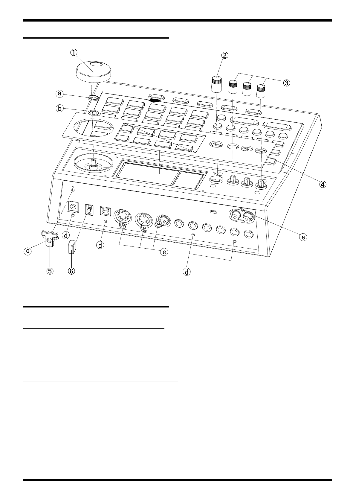
EXPLODED VIEW 1
fig.explo1.eps
EXPLODED VIEW 1 PARTS LIST
[PARTS]
No. PART CODE PART NAME DESCRIPTION Q'TY
1 F2477101 DR-KNOB 1
2 22480260 P R-KNOB MF BLK/LCG 1
3 01340412 P R-KNOB SF-A BLK/LCG 3
4 G2567158 DISPLAY COVER 1
5 F2367103 CORD HOOK 1
6 12499175 BUTTON JSPUE001A 1
[SCREWS]
No. PART CODE PART NAME DESCRIPTION Q'TY
a ********** M9 NUT 1
b ********** M9 WASHER 1
c H5029343 SCREW S-TITE 3X12 BZC 1
d H5029331 SCREW 3X8 BINDING S-TIGHT FEBZC 4
e H5029330 SCREW M3X8 BINDING P-TIGHT BZC 19
4
Page 5
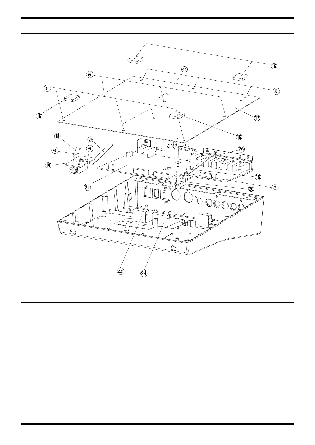
EXPLODED VIEW 2
fig.explo2.eps
DR-880
EXPLODED VIEW 2 PARTS LIST
[PARTS]
No. PART CODE PART NAME DESCRIPTION Q'TY
16 G2357132 FOOT S20 T4 4
17 G2017197 BOTTOM CASE 1
18 G2177303 LEAF M 2
19 ********** INPUT BOARD (included with SW SHEET ASSY) 1
20 ********** HEADPHONES BOARD (included with SW SHEET ASSY) 1
21 78E173M000 MAIN SHEET ASSY 1
24 F3477006 WIRING BNCD-P=1.25-K-22-130 1
25 F3477008 WIRING WIRING INPUT BOARD 1
26 F3477010 WIRING WIRING PHONES BOARD 1
40 F3477007 WIRING BNCD-P=1.00-K-20-140 1
41 G2357117 FOOT T=4MM 15MMX30MM 1
[SCREWS]
No. PART CODE PART NAME DESCRIPTION Q'TY
e H5029330 SCREW M3X8 BINDING P-TIGHT BZC 19
g H5029332 SCREW 3X6 BINDING S-TIGHT FEBZC 3
5
Page 6
Dec.2004
EXPLODED VIEW 3
fig.explo3.eps
EXPLODED VIEW 3 PARTS LIST
[PARTS]
No. PART CODE PART NAME DESCRIPTION Q'TY
11 78E173C000 TOP CASE 1
12 ********** ENCODER BOARD (included with SW SHEET ASSY) 1
13 F5029416 LCD HG1306C-SYL-2 1
14 ********** VR BOARD ASSY (included with MAIN SHEET ASSY) 1
15 G1147703 REAR PLATE 1
22 F3477009 WIRING WIRING PIN JACK BOARD 1
23 F3477011 WIRING WIRING VR BOARD 1
41 F3477012 WIRING WIRING LCD BACK LIGHT 1
42 ******** PIN JACK BOARD (included with SW SHEET ASSY) 1
[SCREWS]
No. PART CODE PART NAME DESCRIPTION Q'TY
e H5029330 SCREW M3X8 BINDING P-TIGHT BZC 11
f H5019431 SCREW P-TITE 3X6 ZC 18
6
Page 7
EXPLODED VIEW 4
fig.explo4.eps
DR-880
EXPLODED VIEW 4 PARTS LIST
[PARTS]
No. PART CODE PART NAME DESCRIPTION Q'TY
7 G2177302 LEAF L 1
8 G2257317 INSULATING SHEET 1
9 78E173S000 SW SHEET ASSY 1
10 G2497004 RUBBER SW 1
11 78E173C000 TOP CASE 1
39 F2449236 FERRITE CORE FS0C320RT01 1
[SCREWS]
No. PART CODE PART NAME DESCRIPTION Q'TY
f H5019431 SCREW P-TITE 3X6 ZC 18
7
Page 8
Dec.2004
TAPE for fixed wring
fig.tape-e.eps
TAPE SIZE
2.0cm
Fixed by Tape
3.5cm
TAPE: 40122645 NITTO FILAMENT TAPE #3883 W19MM 50M 60P (CM)
8
Page 9
LOCATION TO PASTE of FOOT (Inside of Bottom)
fig.bottom-e.eps
Figure for Location to paste.
G2357117
FOOT T=4MM 15X30MM
113mm
DR-880
81mm
0
0
Completion drawing.
139mm
123mm
9
Page 10
Dec.2004
WIRING DIAGRAM
fig.wiring.eps
PIN JACK BOARD
ENCODER
BOARD
WIRING
ENCODER
BOARD
CN2
INPUT BOARD
1
CN5
CN11
CN8
WIRING
INPUT
BOARD
CN11
WIRING
PIN JACK BOARD
CN7
7
CN3
MAIN SHEET ASSY
8
2
BNCD-P=
1.00-K-20-140
3
CN1
CN2
4 5 6
BNCD-P=
1.25-K-22-130
CN1
CN4
WIRING
VOLUME BOARD
CN12
CN6
WIRING
PHONES
BOARD
CN10
HEADPHONES
LCD UNIT
SW SHEET ASSY
VOLUME BOARD
BOARD
WIRING DIAGRAM PARTS LIST
NO PART CODE PART NAME DESCRIPTION Q'TY
1 F3477013 WIRING WIRING ENCODER BOARD 1
2 F3477008 WIRING WIRING INPUT BOARD 1
3 F3477007 WIRING BNCD-P=1.00-K-20-140 1
4 F3477006 WIRING BNCD-P=1.25-K-22-130 1
5 F3477011 WIRING WIRING VR BOARD 1
6 F3477010 WIRING WIRING PHONES BOARD 1
7 F3477009 WIRING WIRING PIN JACK BOARD 1
8 F3477012 WIRING WIRING LCD BACK LIGHT 1
10
Page 11

DR-880
11
Page 12

Dec.2004
PARTS LIST
fig.part1e
SAFETY PRECAUTIONS:
The parts marked have
safety-related characteristics. Use
only listed parts for replacement.
NOTE: The parts marked # are new. (initial parts)
CASING
# G2017197 BOTTOM CASE 1
# G2567158 DISPLAY COVER 1
# G1147703 REAR PLATE 1
# 78E173C000 TOP CASE 1
KNOB,BUTTON
01340412 P R-KNOB SF-A BLK/LCG 3
22480260 P R-KNOB MF BLK/LCG 1
12499175 BUTTON JSPUE001A POWER SW KNOB 1
F2477101 DR-KNOB 1
# G2497004 RUBBER SW SW BOARD 1
SWITCH
# F3129307 PUSH SWITCH SDKLA1-B SW1 1
JACK,EXT TERMINAL
13429825 MIDI CONNECTOR YKF51-5054 2PZ JK2 1
# F3439216 USB JACK YKF45-0021 JK1 1
# F3439217 PIN JACK YKC21-3486 JK3, JK11 1
13449650 PIN JACK YKC21-3045 (DUAL) JK1 1
F3449106 JACK HTJ064-10I JK6,JK7,JK8,JK9, JK10 5
F3449120 6.5MM JACK HTJ-064-10D JK4,JK5 3
13449728 ADAPTOR JACK HEC0740-010010 JK12 1
G2147118 AC JACK HOLDER JK12 1
# G2147820 JACK HOLDER JK4-9 1
Due to one or more of the following reasons,
parts with parts code ******** cannot be supplied as service parts.
• Part supplied only as a component in a complete assembly
• Copyright does not permit the part to be supplied
• Part is sold commercially
The description "Q'TY" means a necessary number of the parts per one product.
DISPLAY UNIT
# F5029416 HG1306C-SYL-2 LCD 1
PWB ASSY
# F2927025 MAIN SHEET ASSY 1
# F2927026 SW SHEET ASSY 1
IC
F5199108 NJM2374AM-TE1 IC(SWITING REGULATOR) IC26 1
# F5179609 MR27V12800J IC P2ROM(WAVE) IC9 1
02900978 M66291GP IC (USB CONTROLLER) IC4 1
F5279861 M12L16161A-7T IC (SDRAM) IC6 1
# F5209173 S-80930CNMC-G80 IC (RESET) IC16 1
# F5199524 UPC29M33AT IC (REGULATOR) IC27 1
# F5229704 PC400T IC (PHOTO COUPLER) IC5 1
F5289102 NJM2100M 8P SOP IC (OP.AMP) IC21 1
# F5289140 M5238AFP-600C IC (OP AMP) IC25 1
F5289139 NJM45564M-TE1 IC (OP AMP) IC19 1
F5279309 BU2090F-E2 IC (LED DRIVER) IC1 1
# ******** MBM29DL164BE-70 IC (FLASH MEMORY) IC13 1
02231767 RA0A-101 (TC223C080AF-101) IC (DSP) IC10 1
03347056 LC32V4265CT-25-TLM-E IC (DRAM) IC12 1
03676990 AK4386VTP-E2 IC (DA) IC23 1
NOTE:MAIN SHEET ASSY includes the follwing parts.
******** VR BOARD ASSY 1
NOTE:SW SHEET ASSY includes the following parts.
******** ENCORDER BOARD ASSY 1
******** INPUT BOARD ASSY 1
******** HEADPHONES BOARD ASSY 1
******** PIN JACK BOARD ASSY 1
12
Page 13

DR-880
IC
02677490 RA0C-003XP7TC203C180AF003 IC (CUSTOM) IC8 1
# 03676856
# F5249108 TC74VHC245FT IC (CMOS) IC2,IC25 2
# F5279314 TC7S04FU IC (CMOS) IC17 1
# F5279315 TC7SH32FU IC (CMOS) IC15,IC28 2
# F5279316 TC7W04FU IC (CMOS) IC7 1
15189261 M5218AFP-600E IC (BIPOLAR OP AMP) IC14,IC20,IC24 3
02900812 AK4353VFP-E2 IC (AD/DA) IC18 1
02451434 AK4552VT IC (AD/DA) IC22 1
TRANSISTOR
F5309115 2SA1241-Y TRANSISTOR Q11 1
15319104 2SA1586-GR(TE85R) TRANSISTOR Q9 1
F5309602 2SB1182 TRANSISTOR Q13 1
15319101 2SC2412KR T146 TRANSISTOR Q10 1
F5319602 2SD1758 TRANSISTOR Q12 1
# F5329529 RN1441 TRANSISTOR Q1,Q2,Q3,Q4,Q5,Q6,Q7,Q8,Q14,Q15 10
15329103 2SK880GR-TE85R FET Q1 1
DIODE
15019525 RD-5.6EB-2 ZENER DIODE D12 1
# F5339318 RD13ESAB2 ZENER DIODE D9,D10 2
# F5339406 KP-1608MGC LED LED1,LED2 2
# F5339405 KP-1608SRC-PRV LED LED4,LED5,LED7,LED9,LED11,LED15,LE
# F5339165 DA204U DIODE ARRAY DA1,DA2,DA3,DA4,DA5,DA6,DA7,DA28 8
# F5339163 DAP202U DIODE ARRAY DA1,DA2,DA3,DA4,DA5,DA6,DA7,DA8,D
F5019203 1N4004 DIODE D6,D8,D11 3
15339119 1SS-352 DIODE D1,D2,D3,D4,D5 5
F5339137 SS14 VF=0.45V DIODE D7 1
UPD703106AGJ-086-UEN (BG324 M)
IC (CPU) IC11 1
D16,LED17
A9,DA10,DA11,DA12,DA13,DA14,DA15,D
A16,DA17,DA18,DA19,DA20,DA21,DA22,
DA23,DA24,DA25,DA26,DA27
8
27
RESISTOR
F5399115 100 J RESISTOR R27,R28,R16,R60 4
F5399145 12K J RESISTOR R164,R165 2
F5399917 22 (1/2W) RESISTOR R20,R93,R109 3
F5399111 22 J RESISTOR R22 1
F5429346 3.3KF 1% RESISTOR R152 1
F5399157 39K J RESISTOR R124,131 2
F5399133 4.7K J RESISTOR R63,R64,R66,R67,R68,R74,R75,R80,R81,R82 10
F5399195 470K J RESISTOR R36,R59,R72,R140 4
F5399158 47K J RESISTOR R138 1
F5399914 6.8KF RESISTOR R96 1
F5399116 82K J RESISTOR R15 1
F5429386 150K F (1608TYPE) MTL.FILM.RESISTOR R107 1
# F5399713 0.56(1/2W) MTL.FILM RESISTOR R147 1
F5399129 1.5K J MTL.FILM RESISTOR R5,R14,R153,R154 4
F5399104 10 J MTL.FILM RESISTOR R31,R65,R92,R5,R6 5
F5399170 100K J MTL.FILM RESISTOR R13,R37,R52,R53,R55,R56,R70,R73,R79,R89,
R90,R95,R101,R108,R117,R119,R123,R127,R
128,R130,R134,R135,R136,R162,R163,R167,
R168
# F5419770 100KX4 MTL.FILM RESISTOR RA18,RA19 2
# F5419758 100X4 MTL.FILM RESISTOR RA3,RA6,RA7 3
F5399140 10K J MTL.FILM RESISTOR R1,R4,R7,R8,R10,R17,R21,R23,R24,R25,R29,
R30,R43,R51,R54,R57,R58,R100,R102,R120,
R121,R137,R139,R300
F5429365 10K OHM F RANK (1%) MTL.FILM RESISTOR R110 1
# F5419759 10KX4 MTL.FILM RESISTOR RA22,RA23,RA25,RA26,RA28 5
# F5399121 180 MTL.FILM RESISTOR R8,R9,R11,R13 4
F5399128 1K J MTL.FILM RESISTOR R76,R78,R84,R86,R91,R99,R112,R116,R125,
R126,R132,R133,R141,R148
F5399200 1M J MTL.FILM RESISTOR R26,R32,R145 3
F5399130 2.2K J MTL.FILM RESISTOR R150 1
F5399190 220K J MTL.FILM RESISTOR R1,R3 2
F5399152 22K J MTL.FILM RESISTOR R97,R114 2
# F5399295 27 MTL.FILM RESISTOR R9,R6 2
# F5399132 3.3K MTL.FILM RESISTOR R35 1
# F5419768 4.7KX4 MTL.FILM RESISTOR RA30 1
# F5399962 43(1/2W) MTL.FILM RESISTOR R69,R71,R155 3
F5399106 47 J MTL.FILM RESISTOR R41,R42,R44,R45,R46,R47,R48,R49,R50,R15
9,R160
# F5399961 470K(1/2W) MTL.FILM RESISTOR R161 1
# F5419763 47X4 MTL.FILM RESISTOR RA12,RA13,RA15,RA17,RA36 5
F5399134 6.8K J MTL.FILM RESISTOR R33,R38,R40 3
F5399109 68 MTL.FILM RESISTOR R15,R19,R20,R21 4
27
28
15
11
13
Page 14

Dec.2004
RESISTOR
# F5419769 68X4 MTL.FILM RESISTOR RA20,RA21,RA24,RA27,RA29,RA31,RA32,
# F5399107 75 MTL.FILM RESISTOR R62 1
# F5399138 8.2K MTL.FILM RESISTOR R118 1
F5429350 562 F 1608 1/10W 5.6K OHM MTL. FILM RESISTOR R151 1
F5429375 47K OHM F RANK (1%) CHIP RESISTOR R103 1
# F3749774 0 CARBON RESISTOR C64 1
POTENTIOMETER
# F3229155 RV110-40E1-15A-B50K VOLUME VR1,VR2,VR3 3
# F3229156 RV142A-40E1-15A-A50K VOLUME VR4 1
CAPACITOR
# F3587451 ERZVA7V330 VARISTOR CAPACITOR C184 1
02341489 ECPU1C474MA5
# F3629696 2.2/50 CHEMICAL CAPACITOR C234 1
F5359732 GRM39B102J50PT CHIP CAPACITOR (1608 TYPE) C75,C76,C77,C78,C101,C130 6
F5359780 GRM39B103K50PT CHIP CAPACITOR (1608 TYPE) C4,C5,C7,C8,C13,C224 6
F5359803 GRM39CH151J50PT CHIP CAPACITOR (1608 TYPE) C70,C81,C82,C83,C186,C2 6
F5359800 GRM39F104Z25PT CHIP CAPACITOR (1608 TYPE) C11,C15,C16,C17,C18,C19,C20,C22,C23,C24
F5359804 GRM39CH221J50PT220P J CHIP CAPACITOR (1608 TYPE) C105 1
# F3639181 1000/35 CHEMICAL CAPACITOR C187,C195 2
13639550KM 100UF/16V CHEMICAL CAPACITOR C124,C127,C138,C189,C192,C193,C194,C1978
# F3629698 4.7/50 CHEMICAL CAPACITOR C167 1
# F3639554 470/16 CHEMICAL CAPACITOR C120,C141,C174,C183 4
# 13639139 470/35 CHEMICAL CAPACITOR C185 1
# F5359827 68P CHEMICAL CAPACITOR C235,C236,C237,C238,C239,C240,C241,C24
13639549 ECA1CM470B CHEMICAL CAPACITOR C63,C129,C144,C153,C176,C199,C201 7
13639602 ECEA1HM010B 1UF/50V CHEMICAL CAPACITOR C71,C146 2
# F5359809 0.0047 CERAMIC CAPACITOR C86,C87,C1 3
F535970601 10P CERAMIC CAPACITOR C84,C85,C115,C131,C133,C134,C157,C168,
# F5359707 15P CERAMIC CAPACITOR C51,C52 2
F3629692 0.22/50V CAPACITOR C69 1
F3629678TS 10/16V CAPACITOR C2,C3,C12,C14,C27,C59,C62,C68,C73,C99,C
13639944TS ECEA1HN100S CAPACITOR C253 1
MYLAR CAPACITOR(SUBMICRON)
RA33,RA34,RA35
C180 1
,C25,C26,C28,C29,C30,C31,C32,C33,C34,C3
5,C36,C37,C38,C39,C40,C41,C42,C43,C44,C
45,C46,C47,C48,C49,C50,C53,C54,C55,C56,
C57,C58,C60,C61,C65,C66,C67,C72,C74,C79
,C80,C88,C89,C90,C91,C92,C93,C94,C95,C9
6,C97,C98,C100,C102,C104,C107,C108,C111
,C123,C125,C147,C149,C150,C152,C154,C15
6,C159,C165,C175,C177,C188,C190,C191,C1
96,C198,C200,C202,C203,C204,C205,C206,C
215,C216,C217,C218,C219,C220,C221,C222,
C223,C228,C230,C231,C232,C233,C249,C25
0,C251,C252,C3,C181,C182,C183,C5,C6
2,C243,C244,C245,C246,C247
C207,C208,C211,C212,C213,C214
103,C106,C109,C112,C113,C117,C119,C121,
C122,C126,C135,C137,C139,C140,C142,C14
3,C151,C155,C158,C161,C162,C163,C166,C1
70,C171,C172,C248,C254,C255
10
114
13
14
39
INDUCTOR, COIL, FILTER
02563501 PT-10 (2280-T008) PULSE TRANS FL1 1
F2569127 MINISMDC075 POLY SWITCH R149 1
F5409102 N1608Z601T02 FERRITE-BEAD L6,L7,L8,L9,L10,19,L20,L21,L22,L23,L29,L3
0,L31,L32,L33,L34,L23,L24,L25,L26,L27
13529246 DSS310-91D223S-50ATL12-134 EMI FILTER FL4,FL2 2
12449386 SBT-0180W EMI FILTER L13 1
# F2449234 TSL1112-471KR72 CHOKE COIL L28 1
# F2449233 ZCYS51R5-M3PAT CHOKE COIL L3 1
CRYSTAL, RESONATOR
F5299114 HC-49SM 5MHZ CRYSTAL X3 1
# F5299315 HC-49SM(6MHZ) CRYSTAL X1 1
02672401 SG-8002JC 67.7376MHZ PC CRYSTAL X2 1
ENCODER
01905467 EVE GC1 F20 24B ROTARY ENCODER EN1 1
CONNECTOR
# F3439220 20FMN-BTK-A CONNECTOR CN1 1
# F3439224 22FE-BT-VK-N CONNECTOR CN2 1
# F3439223 22FE-ST-VK-N CONNECTOR CN1 1
14
21
Page 15

DR-880
CONNECTOR
F3439158 A2001WV2-10P P=2MM CONNECTOR CN4 1
# F3439222 A2001WV2-3P CONNECTOR CN6,CN7,CN11 3
# F3439221 A2001WV2-4P CONNECTOR CN5,CN8 2
WIRING, CABLE
# F3477011 WIRING WIRING VR BOARD CN12 1
# F3477009 WIRING WIRING PIN JACK BOARD CN3 1
# F3477010 WIRING WIRING PHONES BOARD CN10 1
# F3477012 WIRING WIRING LCD BACK LIGHT CN11 1
# F3477008 WIRING WIRING INPUT BOARD CN11 1
# F3477013 WIRING WIRING ENCODER BOARD CN2 1
# F3477006 WIRING BNCD-P=1.25-K-22-130 MAIN - SW 1
# F3477007 WIRING BNCD-P=1.00-K-20-140 MAIN - LCD 1
PICK UP SENSOR
# F2959115 PIEZO PICKUP DB-E648 PIEZO1 1
SCREWS
# H5029343 SCREW S-TITE 3X12 BZC 1
# H5019431 SCREW P-TITE 3X6 ZC 18
H5029330 SCREW M3X8 BINDING P-TIGHT BZC 11
H5029332 SCREW 3X6 BINDING S-TIGHT FEBZC 3
H5029331 SCREW 3X8 BINDING S-TIGHT FEBZC 4
H5019803 SCREW 3X8 BINDING P-TIGHT FECM 11
PACKING
# G2267505 PAD SIDE PAD R 1
# G2267504 PAD SIDE PAD L 1
# G2267515 PAD PAD2 1
# G2267514 PAD PAD1 1
# G2267403 PAD CD PAD 1
# G2617301 OUTER PACKING CASE 1
# G2267405 OUTER SHEET 1
# G2607114 PACKING CASE 1
MISCELLANEOUS
# F2449236 FERRITE CORE FS0C320RT01 1
F2367103 CORD HOOK 1
# G2257317 INSULATING SHEET 1
G2257203 JACK COVER INPUT BOARD JK10 1
# G2177303 LEAF M 2
G2177302 LEAF L 1
# G2357132 FOOT S20 T4 4
ACCESSORIES (Standard)
# G6017379 OWNER’S MANUAL JAPANESE 1
40232389 WARRANTY CARD FOR BOSS JAPAN ONLY 1
00905234 EURO CONVERTER PLUG ECP01-5A 1
# G2457142 AC ADAPTOR BRC-240T 1
G245714101 AC ADAPTOR BRC-230T 1
G2457144 AC ADAPTOR BRC-120T 1
# G2457143 AC ADAPTOR BRC-100T 1
******** RESISTRATION CARD (117V ONLY) 1
# G2567133 SOFTWARE CD-ROM 1
G2357117 FOOT T=4MM 15MMX30MM 1
40122645 NITTO FILAMENT TAPE #3883 W19MM 50MM 60P(CM) 1
G6017380 OWNER’S MANUAL ENGLISH 1
15
Page 16

Dec.2004
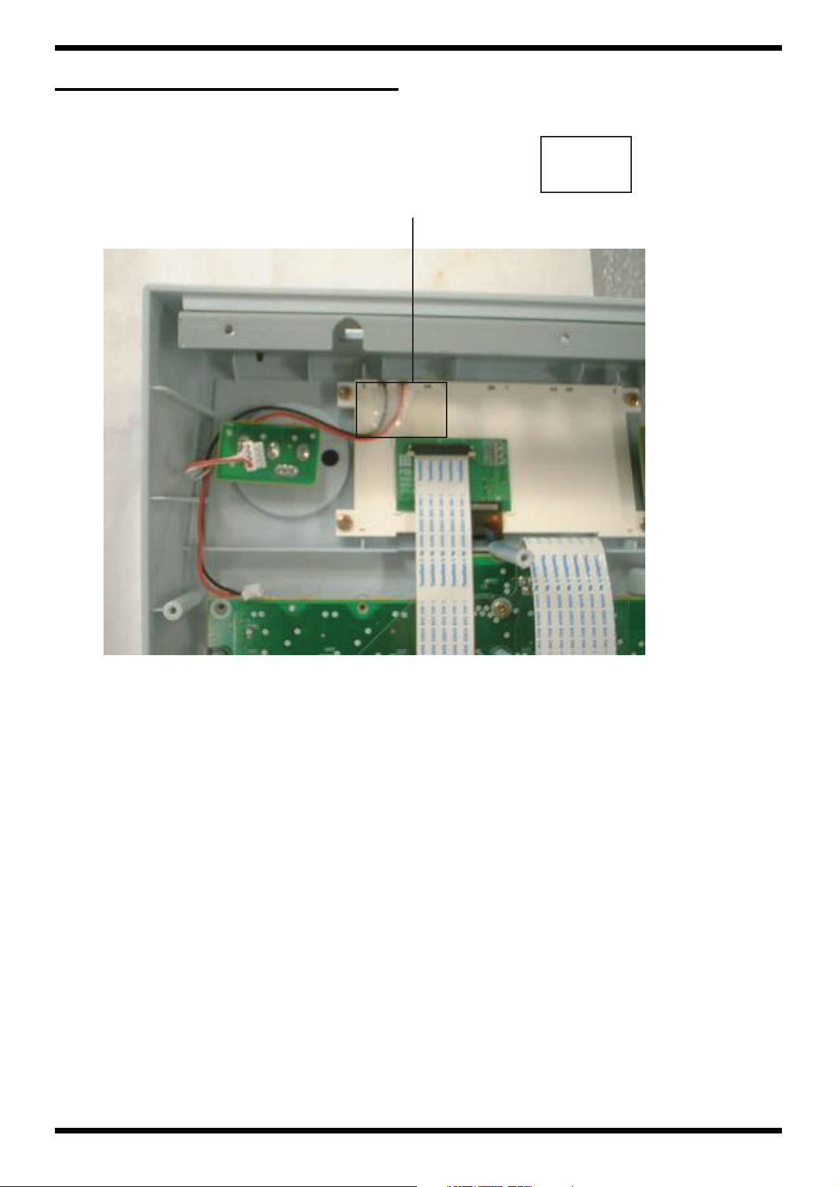
CHECKING THE VERSION NUMBER
While holding down the [RESET][RWD] and [FWD] buttons, power-on the
DR-880.
fig.1version.eps
The version of CPU and FLASH MOMORY will appear .
Computer to DR-880 connection
In order to allow MIDI communication between the DR-880 and your
computer, you must first install the USB MIDI driver.
fig.09-030
(Ex.)
BOSS_DR-880
Removable Disk (*:)
5. Double-click the “BOSS_DR-880” (or “Removable disk (*:)”) icon.
The files from the DR-880 will be displayed on the computer.
File name Contents
SYSTEM.DR8 System settings
UGFX.DR8 Guitar effects user patches
UKIT.DR8 User kits
USEQ.DR8 User patterns and user songs
UTSC.DR8 TSC user patches
6. Copy the files to be backed up into a backup folder on your computer.
It is good practice to create a new folder for the storage of backup data.
7. Close the USB connection.
Windows XP users
Right-click the “BOSS_DR-880” icon (or the “Removable disk (*:)” icon) in My
Computer, and execute “Remove.”
If you are unable to execute the “Remove” operation in this way, proceed as
follows.
1) Click theicon in the task tray, and click the message that indicates “Safely
remove drive (*:)”.
fig.09-200
* The USB MIDI driver is included on the CD-ROM "DR-880 Driver."
USERS DATA SAVE AND LOAD
Backing up the DR-880’s data
Windows users
1. Use a USB cable to connect the DR-880 to your computer.
2. With playback stopped, press [EDIT].
The edit menu screen appears.
3. Move the cursor to the “USB” icon and press [ENTER].
The USB menu screen appears.
4. Move the cursor to the “BACKUP” icon and press [ENTER].
The USB backup screen appears.
If USB Mode is set to “MIDI,” the message “Check USB Mode!” is
displayed, and the SMF Backup screen will not appear. Press [ENTER],
and change the USB Mode to “STORAGE,” and then power it up again
(p. 134).
fig.09-210d
Task bar
2) In the “Safely Remove Hardware” dialog box, click [OK].
Task tray
Windows 2000/Me users
1) Right-click the “BOSS_DR-880” icon (or the “Removable disk (*:)” icon) in
My Computer, and execute “Remove.”
2) Click theicon in the task tray, and click the message that indicates “Safely
remove drive (*:)”.
fig.09-200
Task bar
3) In the “Safely Remove Hardware” dialog box, click [OK].
8. Press [EXIT].
At this point, you can safely disconnect the USB cable from the DR-880
and the computer.
If you press [EXIT] without performing step 7, the message “Disconnect,
OK?” is displayed.
In this case, press [EXIT] and then perform step 7.
If you press [ENTER], the connection between the DR-880 and the
computer will be forcibly terminated. In this case, it is possible that the
backup will be incomplete, making successful recovery impossible.
Task tray
If there is any edited data that has not been saved, the “Cancel edit?” message
will appear.
If you press [ENTER], your edits will be discarded, and the unedited data will
be backed up.
If you press [EXIT], the backup process will be aborted, and you will return to
the USB menu screen.
When connection with the computer has been established, the message will
displayed “Copy data files.”
A “BOSS_DR-880” icon (or a “Removable disk (*:)” icon) will appear on the
computer.
16
Page 17

DR-880
Reading backup data back into the
DR-880 from the computer (Recover)
Windows users
1. Use a USB cable to connect the DR-880 to your computer.
2. With playback stopped, press [EDIT].
The edit menu screen appears.
3. Move the cursor to the “USB” icon and press [ENTER].
The USB menu screen appears.
4. Move the cursor to the “RECOVER” icon and press [ENTER].
The USB recover screen appears.
If USB Mode is set to “MIDI,” the message “Check USB Mode!” is
displayed, and the SMF Recover screen will not appear. Press [ENTER],
and change the USB Mode to “STORAGE,” and then power it up again
(p. 134).
fig.09-220d
When connection with the computer has been established, the message will
displayed “Copy data files.”
A “BOSS_DR-880” icon (or a “Removable disk (*:)” icon) will appear on the
computer.
fig.09-030
(Ex.)
BOSS_DR-880
When the backup data have been recovered, the message will disappear.
At this point, you can safely disconnect the USB cable from the DR-880
and the computer.
If you press [EXIT] without performing step 8, the message “Disconnect,
OK?” is displayed.In this case, press [EXIT] and then perform step 8.
If you press [ENTER], the connection between the DR-880 and the
computer will be forcibly terminated. In this case, it is possible that the
recovery will be incomplete, causing the operation of the DR-880 to later
become unstable.
FACTORY RESET INSTRUCTIONS
You can restore the DR-880 to the condition it was in when it left the factory.
This operation is called “Factory Reset.”
When you execute Factory Reset, the user data will return to its factory-set
condition. If the DR-880 contains important data you want to keep, use Bulk
Dump (p. 131) to save the data on an external MIDI device, or use USB backup
(p. 138) to save the data on the computer before you execute Factory Reset.
1. With playback stopped, press [EDIT].
The edit menu screen appears.
2. Move the cursor to the “FACTORY RESET” icon and press [ENTER].
The display will ask “Factory reset?”
fig.11-010d
Removable Disk (*:)
5. Open the folder on the computer where you have stored the backup data.
6. Select all of the files you want to back into the DR-880.
7. Copy them to the “BOSS_DR-880” icon (or “Removable disk (*:)” icon) on
the computer.
8. Close the USB connection.
Windows XP users
Right-click the “BOSS_DR-880” icon (or the “Removable disk (*:)” icon) in My
Computer, and execute “Remove.”
If you are unable to execute the “Remove” operation in this way, proceed as
follows.
1) Click theicon in the task tray, and click the message that indicates “Safely
remove drive (*:)”.
fig.09-200
Task bar
2) In the “Safely Remove Hardware” dialog box, click [OK].
Task tray
Windows 2000/Me users
1) Right-click the “BOSS_DR-880” icon (or the “Removable disk (*:)” icon) in
My Computer, and execute “Remove.”
2) Click theicon in the task tray, and click the message that indicates “Safely
remove drive (*:)”.
fig.09-200
3. If you’re sure you want to execute Factory Reset, press [ENTER]. If you
decide to cancel without executing, press [EXIT].
The message “Now writing...” will appear, and factory reset will be
executed.
When factory reset have been completed, the message will disappear.
* Do not turn off the power while the message is displayed. Your data may be
damaged if you do so.
Task bar
3) In the “Safely Remove Hardware” dialog box, click [OK].
9. Press [EXIT].
The message “Now writing...” will appear, and the backup data will be
recovered.
Task tray
17
Page 18

Dec.2004
SYSTEM SOFTWARE UPDATING INSTRUCTIONS
Required items
* In order to play back the update data, you will need a means to play back SMF
data.
We recommend a computer + UM-2 + UpdSMF.exe (UpdSMFJ.exe).
In the explanation that follows, we assume that you are using a computer +
UM-2 + UpdSMF.exe (UpdSMFJ.exe).
1. SMF data for the update CD-ROM (#17041565)
_0000001.mid - _0000021.mid
2. SMF playback system
• Computer with USB connector (the UM-2 driver must be installed)
• UM-2
• UpdSMF.exe (English version) or UpdSMFJ.exe (Japanese version)
3. Adaptor BRC series
4. MIDI cable
Update procedure
* As a precaution, please make a backup of the user data before you continue.
1. Connect the MIDI OUT 1 (or 2) of your MIDI playback system (computer
+ UM-2) to the DR-880’s MIDI IN.
2. While holding down [SHIFT] + [EDIT], power-on the DR-880.
fig.system1
Flash-ROM Updater
CPU
1.00 0007 2004/05/13
EXT
1.00 0103 2004/09/27
3. Start up UpdSMF.exe (UpdSMFJ.exe), and make the following settings.
MIDI Out Device =1: EDIROL UM-2 MIDI 1 (or 2)
SMF Path = the directory that contains the update SMF data
4. Click Scan SMF.
Verify that you see the update data (_0000001.mid - _0000021.mid).
5. Click Send.
The update will begin.
* Don’t turn off the power during the update. Doing so may destroy the user
memory.
During the update, the following screens will alternate. The FAVORITE [1]-[4]
button LEDs will blink.
fig.system2
Flash-ROM Updater
adrs 0x00******
fig.system4
Flash-ROM Updater
adrs 0x0044FFF0
sum 0x****
Completed.
sum(prg1)0x****
sum(prg2)0x****
7. Power-off the DR-880.
TEST MODE
Required items
1. Oscillator
2. Oscilloscope
3. Monitor amp
4. Noise meter
5. Ammeter
6. FS-5U
7. EV-5
8. D/A converter
9. Computer
Supported OS: Windows XP/2000/Me or later
10. MIDI cable
11. USB cable
Preparations for test mode
• Oscilloscope settings
TIME/DIV: 1 [msec]
VOLT/DIV: 2 [V]
• Oscillator
1. Waveform: square wavefrequency: 200 [Hz], amplitude: 100 [mVp-p]
2. Waveform: sine wavefrequency: 200 [Hz], amplitude: -10 [dBu]
• Noise meter
FILTER: JIS-A
• FS-5U
Set the POLARITY switch toward the jack.
• EV-5
Set the MIN VR to “0”
• DR-880
GUITAR/BASS INPUT VR = MAX
DRUM VR = MAX
BASS VR = MAX
MASTER VR = MAX
Receiving...
fig.system3
Flash-ROM Updater
adrs 0x00******
sum 0x****
Waiting...
6. When the update is finished, the following display will appear.
Verify the checksum (Prg1, Prg2).
18
Page 19

DR-880
Test items
1. Device check
2. LED check
3. SW check
4. LCD and encoder check
5. Piezo check
6. Volume check
7. Foot switch check
8. Expression check
9. MIDI and USB check
10. Output D/A check
11. AF Gain check
12. Input A/D check
Entering test mode
While holding down the [KIT] and [DISPLAY] buttons, power-on the DR-880.
If the unit is operating correctly, the following display will appear.
fig.devicecheck0.eps
2. LED check
fig.ledcheck1.eps
Verify that all LEDs are lit.
Lit button LED color
1. EFFECT red: 1
2. LOOP red: 1
3. PLAY green: 2
4. REC red: 1
5. FAVORITE 1 red: 1
6. FAVORITE 2 red: 1
7. FAVORITE 3 red: 1
8. FAVORITE 4 red: 1
9. TSC red: 1
fig.ledcheck2.eps
fig.devicecheck1.eps
Press [ENTER] to begin the first test; 1. Device check.
Press [BANK] to proceed to the next test item. Hold down [SHIFT] and press
[FAVORITE 1] to return to the preceding test item.
1. Device check
• Press [FAVORITE 1] to begin the SDRAM check. Verify that a result of
OK appears.
• Press [FAVORITE 2] to begin the FLASH check. Verify that a result of OK
appears.
• Press [FAVORITE 3] to begin the ESP check. Verify that a result of OK
appears.
• Press [FAVORITE 4] to begin the XP check. Verify that a result of OK
appears.
Press [BANK] to proceed to the next test item.
Note any inconsistency in the brightness of the left and right green LEDs.
Note any inconsistency in the brightness of the various red LEDs.
LED/LCD shock test
Drop the rear edge of the unit (marked [] in the illustration) three times from a
height of 5 cm. Then drop the front edge of the unit (marked O in the
illustration) three times from a height of 5 cm. Verify that the LEDs do not go
dark, and that there is no change in the LCD display.
fig.ledcheck3.eps
Press [BANK] to proceed to the next test item.
19
Page 20

Dec.2004
3. SW and LED check
fig.swcheck1.eps
Press the switch whose name is displayed.
For switches that have a lit LED, verify that the LED goes dark when you press
the switch.
fig.swcheck2.eps
4. LCD and Encoder check
fig.lcdencordercheck1.eps
4-1. Adjusting the LCD contrast
Verify that there is no crosstalk in the background and is no unevenness in the
contrast.
If there is a no problem with the contrast.
-> Use [BANK] to proceed to the next test item
If there is a problem with the contrast.
->Make this adjustment, please refer to followings.
Turn the encoder counter-clockwise to lighten the contrast.
Turn the encoder clockwise to darken the contrast.
* The standard setting is "0." It is adjustable in a range from "-4" through "+4".
fig.swcheck3.eps
If you pressed the correct switch.
fig.swcheck4.eps
If you pressed the wrong switch. (Ex. press the KIT)
fig.swcheck5.eps
When you're finished making the setting, press [ENTER]. The display will
indicate "Now Writing," and the setting will be written into memory.
Press the [BANK] switch to proceed to the next test item.
4-2. Slowly turn [VALUE] clockwise for
three clicks.
fig.lcdencordercheck2.eps
Verify that the display changes from 0 -> 1 -> 2 -> 3, and that the contrast
below the characters darkens.
Verify that the characters can still be read even when the contrast is darkest
(third click).
4-3. Slowly turn [VALUE] counterclockwise for three clicks.
fig.lcdencordercheck3.eps
When all have been completed, press [BANK] to proceed to the next test item.
20
Verify that the display changes from 3 -> 2 -> 1 -> 0, that the contrast below the
characters lightens, and that the characters do not disappear.
Press [BANK].
Page 21

DR-880
4-4. PATTERN check
fig.lcdencordercheck4.eps
Check the text encircled in the illustration.
[SONGPATTERN PRESET USER]
Press [BANK].
4-5. PATTERN No. check
fig.lcdencordercheck5.eps
Check the text encircled in the illustration.
[8 8 8]
Press [BANK].
4-6. TEMPO check
fig.lcdencordercheck6.eps
4-8. All Lit check
fig.lcdencordercheck8.eps
Verify that there is no inconsistency, missing characters, gaps, or light patches
in the LCD.
Press [BANK].
4-9. All Dark check
fig.lcdencordercheck9.eps
Verify that no display elements are lit.
Press [BANK].
4-10. Checkerboard pattern check
fig.lcdencordercheck10.eps
Check the text encircled in the illustration.
[8 8 8]
Press [BANK].
4-7. KEY check
fig.lcdencordercheck7.eps
Check the text encircled in the illustration.
[8 1 #b m]
Press [BANK].
fig.lcdencordercheck11.eps
Verify that the checkerboard pattern is not distorted.
fig.lcdencordercheck12.eps
Drop the rear edge of the unit (marked [] in the illustration) three times from a
height of 5 cm, and verify that there is no abnormality in the display.
Press [BANK] to proceed to the next test item.
21
Page 22

Dec.2004
5. Piezo check
fig.piezo.eps
With your finger, lightly strike the pad [RIDE [20, B]] of the DR-880; the
“VALUE” in the LCD will change.
“PEAK” will indicate the peak-hold value.
Gradually increase the force of your strikes until PEAK indicates “OK.”
fig.piezocheck2.eps
Verify that PEAK indicates OK.
Press [BANK] to proceed to the next test item.
6. Volume check
fig.volumecheck4.eps
Set the GUITAR/BASS INPUT VR to the maximum position.
fig.volumecheck5.eps
6-2. Drum VR check
Perform the same test for the DRUM VR. (maximum -> center -> minimum ->
maximum)
fig.volumecheck6.eps
6-1. Guitar/bass input VR check
fig.volumecheck1.eps
Set the GUITAR/BASS INPUT VR to the center position.
fig.volumecheck2.eps
The result will be NG if you move any other volume control.
In this case, set all knobs to the maximum position, and then press the [TSC]
switch to resume from the GUITAR/BASS INPUT VR check.
fig.volumecheck3.eps
6-3. Bass VR check
Perform the same test as you did for the BASS VR. (maximum -> center ->
minimum -> maximum)
fig.volumecheck7.eps
* If desired, you can set all knobs to the maximum position and then press the
[TSC] and resume from the GUITAR/BASS INPUT VR check.
Verify that all VR tests are successfully completed (all OK).
Press [BANK] to proceed to the next test item.
7. Foot Switch check
fig.footswcheck1.eps
Set the GUITAR/BASS INPUT VR to the minimum position.
22
Page 23

DR-880
7-1. Press the FS-5U connected to CTL1
of the CTL 1,2 jack.
fig.footswcheck2.eps
Release the FS-5U.
fig.footswcheck3.eps
7-2. Test CTL2 in the same way. (press
-> release)
fig.footswcheck4.eps
fig.exppedalcheck2.eps
Advance the EV-5 pedal to the maximum position (away from yourself).
fig.exppedalcheck3.eps
Slowly return the EV-5 pedal to the minimum position (toward yourself).
fig.exppedalcheck4.eps
7-3. Test CTL3 in the same way. (press
-> release)
fig.footswcheck5.eps
7-4. Test CTL4 in the same way. (press
-> release)
fig.footswcheck6.eps
Verify that all Foot Switch tests produce a result of OK.
Press [BANK] to proceed to the next test item.
8. Exp Pedal check
Connect an EV-5 to the CTL3,4 EXP PEDAL jack.
Start with the expression pedal lowered (minimum position).
fig.exppedalcheck1.eps
The OK result will not appear unless the center position is detected.
Verify that all results return OK.
Press [BANK] to proceed to the next test item.
9. MIDI and USB test
MIDI
1. Use a MIDI cable to create a loop between MIDI OUT and IN.
2. Press [FAVORITE 1].
3. Verify that that MIDI test result is OK.
USB
1. Use a USB cable to connect the DR-880 to your computer.
2. Press [FAVORITE 2].
3. Verify that the USB test result is OK.
fig.midiusbcheck1.eps
Press the [BANK] switch to proceed to the next test item.
Slowly advance the EV-5 pedal (away from yourself).
23
Page 24

Dec.2004
10. DSP Thru Waveform check
fig.outputdacheck1.eps
10-1. Check the [MASTER OUTPUT]
waveform.
fig.outputdacheck2.eps
10-5. Insert the plug back into
[MASTER OUTPUT] R, and check the
waveform.
fig.outputdacheck4.eps
10-6. Disconnect the plug from
[MASTER OUTPUT] L (MONO), and
check the waveform.
fig.outputdacheck5.eps
VOLT/DIV:2V TIME/DIV:1mS
10-2. Slowly turn [MASTER VOLUME]
toward the minimum position.
Verify that the square wave shown in the illustration from “OUTPUT L/R”
gradually decreases.
10-3. Slowly turn [MASTER VOLUME]
toward the maximum position.
Verify that the square wave shown in the illustration from “OUTPUT L/R”
gradually increases.
* Note: The waveform must not abruptly increase or cut out.
* Note: Misshapen waveforms or waveforms below the nominal level are NG.
10-4. Disconnect the plug from
[MASTER OUTPUT] R, and check the
waveform.
fig.outputdacheck3.eps
10-7. Insert the plug back into
[MASTER OUTPUT] L (MONO), and
check the waveform.
fig.outputdacheck6.eps
24
Page 25

DR-880
10-8. MUTE circuit check
Use [TSC] to switch between MUTE_OFF <--> ON.
fig.outputdacheck7.eps
10-8-1. Check the “MASTER OUTPUT L
(MONO)/R” waveform.
fig.outputdacheck8.eps
10-8-2. Check the [MASTER OUTPUT]
(PIN) waveform.
fig.outputdacheck10.eps
Amplitude: 1.5--1.9 [Vp-p]
mute off
fig.outputdacheck11.eps
mute off
Amplitude: 4.8--6.0 [Vp-p]
fig.outputdacheck9.eps
mute on
mute on
10-8-3. Check the [INDIVIDUAL]
waveform.
fig.outputdacheck12.eps
Amplitude: 1.8--2.3 [Vp-p]
mute off
fig.outputdacheck13.eps
mute on
25
Page 26

Dec.2004
10-8-4. Check the [PHONES]
waveform.
fig.outputdacheck14.eps
Amplitude: 4.9--6.1 [Vp-p]
mute off
fig.outputdacheck15.eps
fig.afgaincheck2.eps
Amplitude: 1.3--1.5 [Vp-p]
Press [BANK] to proceed to the next test item.
12. IN-OUT check, Residual
Noise check
fig.inputadcheck1.eps
mute on
10-8-5. Check the DIGITAL OUT
waveform.
fig.outputdacheck16.eps
Amplitude: 4.0--5.0 [Vp-p]
* It is not necessary to check MUTE.
Press the [BANK] switch to proceed to the next test item.
11. AF Gain check
fig.afgaincheck1.eps
12-1. Check the “MASTER OUT” L
(MONO)/R waveform.
Input a sine wave (200 Hz, -10 dBm) from the “GUITAR/BASS INPUT.”
On your oscilloscope, set VOLT/DIV to 5 [V].
Check the sine wave that is output from “MASTER OUT L (MONO)/R.”
fig.inputadcheck2.eps
VOLT/DIV:5V TIME/DIV:1mS
Amplitude: 9.0--12 [Vp-p]
If distortion is visible in the waveform, the result is NG.
Remove the plug from the “GUITAR/BASS INPUT.”
fig.inputadcheck3.eps
Input a square wave (200 Hz, 100 mVp-p) from the “GUITAR/BASS INPUT.”
Check the square wave that is output from “MASTER OUT L (MONO)/R.”
26
Page 27

12-2. Check the residual noise of
“MASTER OUT” L (MONO)/R.
Listen to the noise, and verify the following.
1. Noise level: -73 dBu or less (both L and R)
2. No abnormal sound is present in the output.
3. No abnormal sound is produced when you apply physical shock to the
unit.
12-3. Check the residual noise of
“MASTER OUT” (PIN).
Listen to the noise, and verify the following.
1. Noise level: -82 dBu or less (both L and R)
2. No abnormal sound is present in the output.
3. No abnormal sound is produced when you apply physical shock to the
unit.
12-4. Check the residual noise of
“INDIVIDUAL.”
Listen to the noise, and verify the following.
1. Noise level: -77.5 dBu or less (both L and R)
2. No abnormal sound is present in the output.
3. No abnormal sound is produced when you apply physical shock to the
unit.
DR-880
12-5. Check the residual noise of
“PHONES.”
Listen to the noise, and verify the following.
1. Noise level: -72 dBu or less (both L and R)
2. No abnormal sound is present in the output.
3. No abnormal sound is produced when you apply physical shock to the
unit.
12-6. Check the residual noise of
“MASTER OUT” L (MONO)/R at the HiGain setting. (INPUT residual noise
check)
Press [BANK] to select “Hi-Gain.”
fig.inputadcheck4.eps
Listen to the noise, and verify the following.
1. Noise level: -70 dBu or less (both L and R)
2. No abnormal sound is present in the output.
3. No abnormal sound is produced when you apply physical shock to the
unit.
13. Turn off the power.
27
Page 28

Dec.2004 DR-880
BLOCK DIAGRAM
fig.block.eps
JK4
USB Controller IC
(MIDI or STRAGE)
MIDI IN
MIDI OUT
SW BOA
RD
ASSY
LCD
LCD BACK LIGHT
LED
VOLUM
E
LCD DRIVER
LED DRI
VER
CPU
UPD703106(V8 50 MA1)
FLASH MEMORY(16M)
DRAM(4M/WO
XP7
TC203C180AF
4
ESP
TC223C080AF-101
DRAM(
4M)
RKING)
CLOCK OUTSYNC
A3.3 V
MASK ROM
(WAVE 128M)
DAC/DIT
CODEC
D3.3 V
A+12V
OUTPUT
VOLUM
AF-AD
E
2
3
1
JK5
2
3
1
D
FOOT SW
FOOT SW 3.4 / EXP
PEDA
L
2
1
D
12
22
11
A
2
4
1
2
4
1
A
2
3
1
A
2
3
1
2
3
1
A
2
4
1
A
1.2
JK3
DIGITAL OUT
JK1 A
OUTPUT L( MONO)
JK1 B
OUTPUT R
JK6
OUTPUT L( MONO)
JK7
OUTPUT R
JK11
PHONES
JK8
INDIVIDUAL A
JK9
INDIVIDUAL B
JK10
GUITAR IN
A-1 2V
POWER
SW1A
12
SW
11
13
JK12
2
1
3
BRC ADAPTOR
AC 14 V
29
Page 29

Dec.2004 DR-880
CIRCUIT BOARD (MAIN BOARD)
fig.b-main1.eps
View from components side
31
Page 30

Dec.2004 DR-880
CIRCUIT BOARD (MAIN BOARD)
fig.b-main2.eps
View from foil side
33
Page 31

Dec.2004 DR-880
CIRCUIT DIAGRAM (MAIN, VOLUME)
fig.c-digital.eps
USB
JK1
YKF45-0021
123
4
10
20
L6
N1608Z601T01
14
12
15
L7
N1608Z601T01
L8
N1608Z601T01
24
22
25
L10
N1608Z601T01
D
6
2
5
4
IC3
N.I.U (SN65220)
D
R13
100k
D
MIDI
JK2
YKF51-5054
45
2
INOUT
45
2
304050
60
To SW BOARD
+
D3.3
2+1
L23
N1608Z601T01
CN2
22FE-BT-VK-N
22
21
20
19
18
17
16
15
14
13
12
11
10
9
8
7
6
5
4
3
2
1
A
L33
N1608Z601T01
22
21
20
19
18
17
16
15
14
13
12
11
10
9
8
7
6
5
4
3
2
1
C79
0.1
C205
0.1
SW_DATA7
SW_DATA6
SW_DATA5
SW_DATA4
SW_DATA3
SW_DATA2
SW_DATA1
SW_DATA0
LED_DATA
LED_CLOCK
D
A
C71
1/50
2+1
84
-
+
IC14C
M5218AFP
CN4
A2001WV2-10P
2-1
To VOLUME BOARD
L1
N.I.U
L2
N.I.U
1
NC
A
GND
GND
NC3B
C9
N.I.U
C21
N.I.U
R20
+
D3.3
22(1/2W)
L9
N1608Z601T01
D
C218
C216
0.1
0.1
C219
C217
0.1
0.1
To Flash Writer
R33
6.8k
R38
6.8k
R40
6.8k
6
5
A
+
1
1
2
2
3
3
4
4
5
5
6
6
7
7
8
8
9
9
10
10
A
C220
0.1
C221
0.1
1 2
1 2
R32 1M
2
-
3
+
A
-
+
IC14B
M5218AFP
C229
N.I.U
C10
N.I.U
R15
120
R16
100
D
1 8
2 7
3 6
4 5
1 8
2 7
3 6
4 5
C222
0.1
1
IC14A
M5218AFP
R35
3.3k
3
7
VROUT_R
VRIN_R
VRIN_L
VROUT_L
D13
N.I.U
DD
R22
22
RA12
47x4
RA13
47x4
D12
RD5.6EB2
1 2
21
L3
3 4
2 5
1 6
L4
N.I.U
D1
1SS352
1 2
D2
1SS352
R42
47
134
DA1
DA204U
D
RA18
100kx4
DA3
DA204U
R44
47
C81
150p
To ENCODER BOARD
+
D3.3
6
IC5
PC400T
3
2
A1
3
A2
4
A3
5
A4
6
A5
7
A6
8
A7
9
A8
19
G
1
DIR
C206
0.1
4 5
R34
1k
C69
0.22/50
R45
47
C82
150p
CN5
A2001WV2-4P
ZCYS51R5-M3PAT
D3.3
C15
0.1
5
+
D3.3
21
62
IC7C
TC7W04FU
+
D3.3
IC25
TC74VHC245FT
20
B1
B2
VCC
B3
B4
B5
B6
B7
B8
GND
10
D
1 8
2 7
3 6
3 6
4 5
D
CN3
N.I.U(B7B-PH-K-S)
7
7
6
6
5
5
4
4
3
3
2
2
1
1
+
D3.3
C64
0
R36
470k
A
C75
0.001
C83
150p
1
1
2
2
3
3
4
4
D
C12
10/16
+
R14
1.5k
D
D3.3
17
IC7A
TC7W04FU
18
17
16
15
14
13
12
11
RA19
100kx4
1 8
2 7
+
D3.3
DA2
DA204U
2 1
3
R37
100k
A
C76
0.001
+
D3.3
R53
100k
R52
100k
D
Reset
R5
1.5k
C6
N.I.U
C13
0.01
D
+
R21
10k
MODE2
XRST
D
FS4
FS3
C70
FS2
150p
FS1
C77
0.001
R56
100k
R55
100k
C86
0.0047
IC16
S-80930CNMC-G80
D
C78
0.001
C87
0.0047
D
C100
0.1
+
D3.3
84
C48
0.1
SW_SCAN6
SW_SCAN5
SW_SCAN4
SW_SCAN3
SW_SCAN2
SW_SCAN1
SW_SCAN0
+
D3.3
D
ENCA
ENCB
+
D3.3+D3.3
2
VDD
5
OUT
CD
NC
VSS
3
DD
IC7D
D
TC7W04FU
R31
10
C63
47/16
ESP_INT0
LED_CLOCK
C89
0.1
1
4
IC7B
3 5
TC7W04FU
+
C227
N.I.U
C226
CDTI
CCLK
CSN
MUTE
PDN
XP_INT
SW_SCAN6
SW_SCAN5
SW_SCAN4
SW_SCAN3
SW_SCAN2
SW_SCAN1
SW_SCAN0
XP_RST
LED_DATA
R6
27
R9
27
R18
N.I.U
C228
0.1
C225
N.I.U
N.I.U
C84
10p
X3
HC-49SM(5MHz)
C85
10p
D3.3
R58
10k
MAIN BOARD
(Digital)
+
+
D3.3
D
D+
D-
VBUS
TRON
INT1/SOF
INT0
DACK1
DREQ1
DREQ0
DACK0
TC1
TEST
RST
D3.3
12
35
1
16
IO-VCC
IO-VCC
CORE-VCC
CORE-VCC
HWR/BYTE
GND
GND
GND
2
15
36
D
PCM1/CLKOUT/BUSCLK
PCT1/UCAS/UWR/UDQM
PCT0/LCAS/LWR/LDQM
PCS6/CS6/RAS6
PCS5/CS5/IORD
PCS4/CS4/RAS4
PCS3/CS3/RAS3
PCS2/CS2/IOWR
PCS1/CS1/RAS1
PCD3/UBE/SDRAS
PCD2/LBE/SDCAS
VSS
VSS
VSS
VSS
VSS
VSS
9
28
38
48
82
99
113
IC4
M66291GP
A6
A5
A4
A3
A2
A1
D15/A0
D14/P6
D13/P5
D12/P4
D11/P3
D10/P2
D9/P1
D8/P0
D7
D6
D5
D4
D3
D2
D1
D0
CS
LWR
RD
XIN
XOUT
R27
100
C51
15p
PAH9/A25
PAH8/A24
PAH7/A23
PAH6/A22
PAH5/A21
PAH4/A20
PAH3/A19
PAH2/A18
PAH1/A17
PAH0/A16
PAL15/A15
PAL14/A14
PAL13/A13
PAL12/A12
PAL11/A11
PAL10/A10
PAL9/A9
PAL8/A8
PAL7/A7
PAL6/A6
PAL5/A5
PAL4/A4
PAL3/A3
PAL2/A2
PAL1/A1
PAL0/A0
PDL15/D15
D14/PDL14
D13/PDL13
D12/PDL12
D11/PDL11
D10/PDL10
D9/PDL9
D8/PDL8
D7/PDL7
D6/PDL6
D5/PDL5
D4/PDL4
D3/PDL3
D2/PDL2
D1/PDL1
D0/PDL0
PCM0/WAIT
PCM4/REFRQ
PCM3/HLDRQ
PCM2/HLDAK
PCT7/BCYST
PCT6/OE
PCT5/WE
PCT4/RD
PCS7/CS7
PCS0/CS0
PCD1/SDCLK
PCD0/SDCKE
VPP/MODE2
MODE1
MODE0
VSS
VSS
VSS
125
135
+
C88
0.1
D
C101
0.001
D
C2
10/16
C4
0.01
C7
0.01
R17
+
D3.3
10k
R19 N.I.U
+
D3.3
R23
10k
XRST
IC11
UPD703106AGJ-086-UEN
49
ADTRG/IP123/P37
50
IP122/P36
51
IP121/P35
52
RXD2/IP120/P34
53
TXD2/IP133/P33
54
SCK2/IP132/P32
55
SI2/IP131/P31
56
SO2/IP130/P30
65
SCK1/P45
66
RXD1/SI1/P44
67
TXD1/SO1/P43
68
SCK0/P42
69
RXD0/SIO/P41
70
TXD0/SO0/P40
71
AVDD/AVREF
72
AVSS
73
P77/ANI7
74
P76/ANI6
75
P75/ANI5
76
P74/ANI4
77
P73/ANI3
78
P72/ANI2
79
P71/ANI1
80
P70/ANI0
19
DRQ3/IP103/P07
20
DRQ2/IP102/P06
21
DRQ1/IP101/P05
22
DRQ0/IP100/P04
23
TO00/P03
24
IP001/P02
25
TIO00/IP000/P01
26
PWM0/P00
29
DMAAK3/PBD3
30
DMAAK2/PBD2
31
DMAAK1/PBD1
32
DMAAK0/PBD0
33
TO01/P13
34
IP011/P12
35
TIO10/IP010/P11
36
PWM1/P10
39
TC3/IP113/P27
40
TC2/IP112/P26
41
TC1/IP111/P25
42
TC0/IP110/P24
43
TO02/P23
44
IP021/P22
45
TIO20/IP020/P21
46
NMI/P20
D
83
P52/TO03
84
P51/IP031
85
P50/IP030/TI030
86
PCM5/SELFREF
60
CKSEL
62
X2
63
1 2
X1
CPU V850 MA1
61
CVDD
64
CVSS
59
RESET
XRST
4
3
5
6
11
42
8
9
47
48
10
7
D
46
C3
10/16
C5
0.01
C8
0.01
D
22
21
20
19
18
17
40
39
38
37
34
33
32
31
30
29
28
27
26
25
24
23
45
44
41
43
14
13
VDD
VDD
VDD
VDD
VDD
VDD
VDD
VDD
VDD
A6
A5
A4
A3
A2
A1
D15
D14
D13
D12
D11
D10
D9
D8
D7
D6
D5
D4
D3
D2
D1
D0
CS6
R26
1M
X1
HC-49SM(6MHz)
114
115
116
117
118
119
120
121
122
123
126
127
128
129
130
131
132
133
136
137
138
139
140
141
142
143
144
1
2
3
4
5
6
7
10
11
12
13
14
15
16
17
90
91
87
88
89
92
93
94
95
96
97
100
101
102
103
104
105
106
107
108
109
110
111
D3.3
18
57
58
D3.3
134
124
112
98
81
37
47
27
8
C90
0.1
12
+
D
+
C91
0.1
18
27
36
45
18
27
36
45
18
27
36
45
18
27
36
45
18
27
36
45
18
27
36
45
18
27
36
45
18
27
36
45
18
27
36
45
18
27
36
45
D3.3
C52
15p
D
A22
A21
A20
A19
A18
A17
A16
A15
A14
A13
A12
A11
A10
A9
A8
A7
A6
A5
A4
A3
A2
A1
A0
RA32
68x4
RA33
68x4
RA34
68x4
RA35
68x4
R46 47
R49 47
R50 47
+
C92
0.1
D3.3
D15
D14
D13
D12
D11
D10
D9
D8
D7
D6
D5
D4
D3
D2
D1
D0
+
D3.3
R300
10k
RA20
68x4
RA21
68x4
RA24
68x4
RA27
68x4
RA29
68x4
RA31
68x4
D15
D14
D13
D12
D11
D10
D9
D8
D7
D6
D5
D4
D3
D2
D1
D0
MODE2
R54
10k
D
+
+
D3.3+D3.3+D3.3+D3.3
C93
C94
C95
0.1
0.1
0.1
D DD DDD DD DD
+
D3.3
R1
C234
2.2/50
10k
C239
C247
C238
C235
C237
C236
68p
68p
D
D
D
D
+
D3.3
+
D3.3
C30 0.1
C35 0.1
C40 0.1
1
11
33
45
66
77
89
121
VDD5
VDD5
VDD5
VDD544VDD5
VDD5
VDD5
VDD588VDD5
XP7
VSS
VSS
VSS
VSS
VSS
VSS
VSS
VSS
VSS
VSS
6
15
VSS
17
39
51
61
63
72
83
96
105
117
C45 0.1
12
56
100
132
133
144
165
176
WA23
VDD3
VDD3
VDD3
VDD5
VDD5
VDD5
VDD3
VDD5
VDD5
WA22
WA21
WA20
WA19
WA18
WA17
WA16
WA15
WA14
WA13
WA12
WA11
WA10
WA9
WA8
WA7
WA6
WA5
WA4
WA3
WA2
WA1
WA0
WD15
WD14
WD13
WD12
WD11
WD10
WD9
WD8
WD7
WD6
WD5
WD4
WD3
WD2
WD1
WD0
WCS7
WCS6
WCS5
WCS4
WCS3
WCS2
WCS1
WCS0
WOE1
WOE0
WREQ
WACK
OUTP2
OUTP1
OUTP0
WCKC
BCKC
SDOD
SDOC
WCKB
BCKB
SDIB
SDOB
WCKA
BCKA
SDIA5
SDIA4
SDIA3
SDIA2
SDIA1
SDIA0
SDOA5
SDOA4
SDOA3
SDOA2
SDOA1
VSS
127
SDOA0
VSS
VSS
VSS
VSS
VSS
VSS
VSS
VSS
IC8
131
134
140
149
157
164
171
TC203C180AF003(XP7)
D
WAVE ROM(128Mbit)
DD
67
68
70
69
71
73
95
92
90
86
84
81
79
76
74
75
78
80
82
85
87
91
94
93
99
WD15
104
WD14
109
WD13
113
WD12
116
WD11
112
WD10
108
WD9
103
WD8
102
WD7
107
WD6
111
WD5
115
WD4
114
WD3
110
WD2
106
WD1
101
WD0
126
125
124
123
122
120
119
118
97
98
128
129
13
10
14
9
8
7
5
4
3
2
175
174
173
166
167
168
169
170
172
158
159
160
161
162
163
36
12
13
11
14
15
10
16
17
18
19
20
21
22
23
24
27
R47 47
R48 47
2
3
4
5
6
7
8
9
1
D3.3
18
27
36
45
IC9
MR27V12800J
A22
A21
A20
A19
A18
A17
A16
A15
A14
A13
A12
A11
A10
A9
A8
A7
A6
A5
A4
A3
A2
A1
A0
CE
OE
BYTE
+
RA36
47x4
68p
XCS
XRESET
A0
XWR
XRD
D0
D1
D2
D3
D4
D5
D6
D7/SI
DUTY0
DUTY1
VOUT
VDD
VSS
C86
P/S
+
D3.3
C74
0.1
TRS5
TRS4
TRS3
TRS2
TRS1
TRS0
TRR5
TRR4
TRR3
TRR2
TRR1
TRR0
68p
20
19
18
17
16
15
14
13
12
11
10
D
+
D3.3
68p
C240
68p
CN1
20FMN-BTK-A
20
19
18
17
16
15
14
13
12
11
10
9
9
8
8
7
7
6
6
5
5
4
4
3
3
2
2
1
1
D15/A-1
VCC
VCC
VSS
VSS
VSS
VSS
18
27
36
45
18
27
36
45
18
27
36
45
18
27
36
45
4
VDD
GND2OUT
D
68p
C242
C241
68p
To LCD
46
44
D14
42
D13
40
D12
35
D11
33
D10
31
D9
29
D8
45
D7
43
D6
41
D5
39
D4
34
D3
32
D2
30
D1
28
D0
38
37
48
47
26
25
WD15
WD7
WD14
WD6
WD13
WD5
WD12
WD11
WD3
WD10
WD8
WD0
WD1
WD9
WD2
WD4
ESP_INT0
X2SG-8002JC(67.7376MHz)
ESP_DA5
ESP_DA3
ESP_DA1
ESP_AD
ESP_LRCK
ESP_BCK
ESP_MCK
C246
C245
C244
C243
68p
68p
68p
68p
68p
WD15
WD14
WD13
WD12
WD11
WD10
WD9
WD8
WD7
WD6
WD5
WD4
WD3
WD2
WD1
WD0
+
D3.3
C61
C60
0.1
0.1
RA22
10kx4
RA25
10kx4
RA28
10kx4
RA30
4.7kx4
1
OE
3
D7
C62
D6
10/16
D5
D4
D3
+
D3.3
D2
D1
D
D0
R30
10k
CS4
+
D3.3
H/L
R41
47
R159 47
R160 47
+
D3.3
A0
R24
10k
R25
10k
C96
0.1
+
D3.3
53
C215
0.1
1
4
2
IC28
TC7SH32FU
D
D0
D1
D2
D3
D4
D5
D6
D7
D3.3
18
27
36
45
18
27
36
45
18
27
36
45
18
27
36
45
+
D3.3
+
CS1
C97
0.1
+
D3.3
C98
0.1
D3.3
D3.3
RA8
N.I.U
RA9
N.I.U
RA10
N.I.U
RA11
N.I.U
SDRAM(16Mbit)
IC6
M12L16161A-7T
20
A11
A10/AP
32
A10
A9
31
A9
A8
30
A8
A7
29
A7
A6
28
A6
A5
27
A5
A4
24
A4
A3
23
A3
A2
22
A2
A1
21
A1
A0
18
CS
17
RAS
16
CAS
15
WE
19
A20
BA
36
UDQM
14
LDQM
37
NC/RFU
34
CKE
35
CLK
33
NC
FLASH MEM(16Mbit)
13
A22
10
A21
9
A20
16
A19
17
A18
48
A17
1
A16
2
A15
3
A14
4
A13
5
A12
6
A11
7
A10
8
A9
18
A8
19
A7
20
A6
21
A5
22
A4
23
A3
24
A2
25
A1
26
CS0
11
28
15
47
14
12
D3.3
R43
10k
D
+
D3.3
R51
10k
XRST
+
C99
10/16
+
19
D
49
DQ15
48
DQ14
46
DQ13
45
DQ12
43
DQ11
42
DQ10
40
DQ9
39
DQ8
12
DQ7
11
DQ6
9
DQ5
8
DQ4
6
DQ3
5
DQ2
3
DQ1
2
DQ0
1
VDD
25
VDD
7
VDDQ
13
VDDQ
38
VDDQ
44
VDDQ
4
VSSQ
10
VSSQ
41
VSSQ
47
VSSQ
26
VSS
50
VSS
C53
0.1
NC(A21)
NC(A20)
A19
A18
A17
A16
A15
A14
A13
A12
A11
A10
A9
A8
A7
A6
A5
A4
A3
A2
A1
A0
CE
WE
OE
RY/BY
BYTE
WP/ACC
RESET
IC13
MBM29DL164BE-70
+
2
3
4
5
6
7
8
9
1
C54
0.1
DQ15/A-1
45
+
D3.3
D
D3.3
R4 10k
D15
D14
D13
D12
D11
D10
D9
D8
D7
D6
D5
D4
D3
D2
D1
D0
+
R7 10k
R8 10k
R10 10k
A13
A12
A11
A10
A9
A8
A7
A6
A5
A4
A3
A2
A1
A0
36
27
18
RA3
100x4
RA6 100x4
C14 10/16
C17 0.1
C19 0.1
C24 0.1
C29 0.1
C34 0.1
C39 0.1
C44 0.1
27
25
23
21
22
24
26
28
29
30
31
32
34
35
36
41
47
52
55
50
46
40
38
43
49
54
53
48
42
37
60
58
CS3
19
20
57
62
64
59
147
150
152
154
156
155
153
151
148
130
135
136
137
138
139
141
142
145
146
143
18
16
65
R57
10k
D
18
27
36
45
18
27
36
45
RA7100x4
C16 0.1
C18 0.1
C22 0.1
C26 0.1
C32 0.1
C37 0.1
C42 0.1
CA13
CA12
CA11
CA10
CA9
CA8
CA7
CA6
CA5
CA4
CA3
CA2
CA1
CA0
CD15
CD14
CD13
CD12
CD11
CD10
CD9
CD8
CD7
CD6
CD5
CD4
CD3
CD2
CD1
CD0
AS
CS
RW
DS
WAIT
INT
CK
RESET
EA8
EA7
EA6
EA5
EA4
EA3
EA2
EA1
EA0
ED7
ED6
ED5
ED4
ED3
ED2
ED1
ED0
RAS
CAS
EWE
SYI
SYO
TEST
XRST
+
D3.3
IC2
TC74VHC245FT
20
18
A1
B1
17
A2
B2
VCC
16
A3
B3
15
A4
B4
14
A5
B5
13
A6
B6
12
A7
B7
11
A8
B8
+
D3.3
G
DIR
C11
0.1
1
2
C55
0.1
DQ14
DQ13
DQ12
DQ11
DQ10
DQ9
DQ8
DQ7
DQ6
DQ5
DQ4
DQ3
DQ2
DQ1
DQ0
VDD
VSS
VSS
D3.3
GND
10
C56
0.1
45
43
41
39
36
34
32
30
44
42
40
38
35
33
31
29
37
27
46
+
53
IC15
TC7SH32FU
D
N1608Z601T01
D
C57
C58
0.1
0.1
C72
0.1
4
C80
0.1
D15
D14
D13
D12
D11
D10
D9
D8
D7
D6
D5
D4
D3
D2
D1
D0
XP_INT
XP_RST
L34
C248
10/16
D15
D14
D13
D12
D11
D10
D9
D8
D7
D6
D5
D4
D3
D2
D1
D0
+
D3.3
C59
10/16
+
D3.3
D
C73
10/16
D
+
VR1A
3
RV110-40E1(50kB)
2
1
VR2A
3
RV110-40E1(50kB)
2
1
VR3A
3
RV110-40E1(50kB)
2
1
13
14
24
23
22 12
1
A
VR4A
RV142A-40E1(50kA)
1
1
2
2
3
3
4
4
5
5
6
6
7
To MAIN BOARD
7
8
8
9
9
10
10
CN12
WIRING VR BOARD
VOLUME BOARD
+
D3.3
C27
10/16
D
1
11
26
37
51
73
90
VDD5
VDD5
VDD5
VDD5
VDD5
VDD5
CA13
CA12
CA11
CA10
CA9
CA8
CA7
CA6
CA5
CA4
CA3
CA2
CA1
CA0
CD7
CD6
CD5
CD4
CD3
CD2
CD1
CD0
INT1
INT0
CS
WR
RD
DIRECT
CTYPE
EAMPX
RFRSH
PWRSAV
GRAMC
SHRMD
OSC
DA7
DA6
DA5
DA4
DA3
DA2
DA1
DA0
AD3
AD2
AD1
AD0
LRCK1
LRCK0
BCK1
BCK0
MCK1
MCK0
XTESTT
XTESTS
TESTB
VSS
6
15
VSS
VSS
22
29
ESP4
VSS
VSS
VSS
36
44
55
VDD5
VSS
81
A13
82
A12
83
A11
84
A10
86
A9
87
A8
88
A7
89
A6
91
A5
92
A4
94
A3
95
A2
96
A1
97
A0
99
100
102
103
104
105
106
107
74
75
77
78
79
65
66
67
68
69
70
71
D
30
118
119
121
122
123
125
126
127
129
130
132
133
134
135
137
64fs
138
256fs
139
141
76
131
31
C204 0.1
C20 0.1
C23 0.1
C25 0.1
C28 0.1
C31 0.1
C33 0.1
C36 0.1
C38 0.1
C41 0.1
C43 0.1
C46 0.1
C47 0.1
C49 0.1
C50 0.1
18
59
93
101
109
120
128
140
IC10
TC223C080AF-101(ESP4)
VDD3
VDD3
VDD3
VDD5
VDD5
VDD5
VDD3
VDD5
63
TRR5
62
TRR4
61
TRR3
60
TRR2
58
TRR1
57
TRR0
56
TRCKIN
52
RST2
53
RST1
R28 100
54
VPOUT
110
TRS5
111
TRS4
112
TRS3
113
TRS2
114
TRS1
115
TRS0
117
TRCKO
142
SYO
143
SYI
28
EA9
27
EA8
25
EA7
24
EA6
23
EA5
21
EA4
20
EA3
19
EA2
17
EA1
16
EA0
50
ED23
49
ED22
48
ED21
47
ED20
46
ED19
45
ED18
43
ED17
42
ED16
41
ED15
40
ED14
39
ED13
38
ED12
35
ED11
34
ED10
33
ED9
32
ED8
10
ED7
9
ED6
8
ED5
7
ED4
5
ED3
4
ED2
3
ED1
2
ED0
12
WE
13
CAS
14
RAS
VSS
VSS
VSS
VSS
VSS
VSS
VSS
VSS
VSS
64
VSS
72
80
85
98
108
116
124
136
144
D
RA15
47x4
18
27
36
45
18
27
RA17
36
47x4
45
EA8
EA7
EA6
EA5
EA4
EA3
EA2
EA1
EA0
ED7
ED6
ED5
ED4
ED3
ED2
ED1
ED0
C249
0.1
A
33.8688MHz
20
VR1B
RV110-40E1(50kB)
10
20
VR2B
RV110-40E1(50kB)
10
20
VR3B
RV110-40E1(50kB)
10
VR4B
10
20
RV142A-40E1(50kA)
A
D
XRST
C224
0.01
D
+
D3.3
R29
DRAM(4Mbit)
10k
IC12
LC32V4265CT-25-TLM-E
28
A8
I/O16
27
A7
I/O15
26
A6
I/O14
25
A5
I/O13
24
A4
I/O12
21
A3
I/O11
20
A2
I/O10
19
A1
18
A0
13
NC
14
NC
17
NC
32
NC
16
RAS
30
UCAS
31
LCAS
15
WE
29
OE
D
TRR5
TRR4
TRR3
TRR2
TRR1
TRR0
TRS5
TRS4
TRS3
TRS2
TRS1
TRS0
+
D3.3
43
1 8
RA23
42
2 7
10kx4
41
3 6
40
4 5
38
1 8
RA26
37
2 7
10kx4
3 6
36
35
4 5
I/O9
10
I/O8
9
I/O7
8
I/O6
7
I/O5
5
I/O4
4
I/O3
3
I/O2
2
I/O1
22
VCC
6
VCC
1
VCC
44
VSS
39
VSS
23
VSS
C65
0.1
ED7
ED6
ED5
ED4
ED3
ED2
ED1
ED0
+
D3.3
C68
10/16
D
C67
C66
0.1
0.1
35
Page 32

Dec.2004 DR-880
CIRCUIT DIAGRAM (JACK)
fig.c-analog.eps
JK4
HTJ-064-10D
2
FOOTSW 1,2
3
1
FOOTSW 3,4 / EXP PEDAL
JK5
HTJ-064-10D
2
3
1
2+1
R93
22(1/2W)
C127
100/16
CN8
A
A2001WV2-4P
1
1
2
2
3
3
4
4
R109
C138
22(1/2W)
100/16
A
2-1
To INPUT BOARD
IC21C
NJM2100M
+
D3.3+D3.3
DA4
DA204U
2 1
R59
470k
+
D3.3+D3.3
D
R66
4.7k
+
D3.3+D3.3
R72
470k
D
R80
4.7k
R100
C130
10k
0.001
R103
C135
47k(F-rank)
10/16
+
A3.3
C214
10p
R118
8.2k
84
C150
0.1
+
R121
10k
C151
10/16
A
AAAA A
R63
4.7k
R67
4.7k
R74
4.7k
R81
4.7k
D3.3+D3.3
2
3
C152
0.1
+
R96
6.8k(F-rank)
C131
10p
-
+
IC21A
NJM2100M
3
DA5
DA204U
2 1
3
DA6
DA204U
2 1
3
DA7
DA204U
2 1
3
1
C153
47/16
R64
4.7k
R68
4.7k
R75
4.7k
R82
4.7k
R110
10k(F-rank)
D
FS1
D
FS2
ESP_LRCK
ESP_BCK
ESP_DA5
ESP_MCK
CDTI
CCLK
CSN
D
FS3
PDN
D
FS4
C133
10p
R107
150k(F-rank)
6
7
5
+
C213
10p
IC21B
NJM2100M
ESP_DA1
ESP_DA3
DAC/DIT
R60
100
C106
10/16
C123
0.1
A
C137
10/16
C139
10/16
DAC
A
+
A3.3
R65
10
3
TX
DVDD
LRCK
BICK
SDTI
MICKO
MCKI5AOUTR
SDA/CDTI
SCL/CCLK
CSN
I2C
CAD1
CAD0
TTL
DZF
PDN
TST
NC
DVSS
4
R92
10
C126
10/16
A
2
LIN
1
RIN
9
SDTI
10
LRCK
11
MCLK
12
BCLK
7
DEM1
6
DEMO
13
PDN
12
VCOM
11
LOUT
10
ROUT
9
DIF0
16
PM
15
DIF1
C232
0.1
D
22
AVDD
AOUTL
VCOM
AVSS
21
A
AD
+
A3.3
CODEC
IC22
AK4552VT
4
5
VA
VD
LOUT
ROUT
SDTO
VCOM
VSS
3
C223
0.1
A
C165
0.1
A
C108
0.1
19
18
C111
0.1
20
IC18
AK4353VFP-E2
15
16
8
14
C166
10/16
C109
10/16
C230 0.1
DDA
C231 0.1
A
C112
10/16
C254
10/16
C255
10/16
ESP_AD
C147
C146
0.1
1/50
A
D
C167
4.7/50
2+1
C149
84
0.1
-
+
C154
IC20C
0.1
M5218AFP
R164
12k
R167
100k
1
A
R165
R168
12k
100k
1
A
C161
10/16
C170
10/16
A
2-1
C115
10p
R83
N.I.U
R89
R91
C119
10/16
Q14
RN1441
2 3
A
C140
10/16
Q15
RN1441
2 3
A
R122
N.I.U
R124
39k
C209
N.I.U
R129
N.I.U
R131
39k
C210
N.I.U
IC24C
M5218AFP
100k
1k
6
-
5
+
C212
IC20B
10p
M5218AFP
A
C134
10p
R104
N.I.U
R112
1k
2
-
3
+
C211
10p
A
C157
10p
C160
N.I.U
R123
100k
6
7
5
+
IC24B
M5218AFP
C168
10p
C169
N.I.U
R130
100k
2
1
3
+
IC24A
M5218AFP
2+1
A
84
C1750.1
-
+
0.1
C177
2-1
7
R108
100k
IC20A
M5218AFP
C155
10/16
C158
10/16
C116
N.I.U
C121
10/16
VRIN_L
C136
N.I.U
C142
10/16
1
VRIN_R
R125
C162
1k
10/16
R127
100k
AA
R132
C171
1k
10/16
R134
100k
A
A
VROUT_L
IC19C
NJM4556AM
VROUT_R
2+1
C156
84
0.1
-
+
C159
AA
0.1
2-1
R87
N.I.U
A
C207
C122
10p
10/16
R95
100k
R105
N.I.U
A
C208
10p
C143
10/16
R117
100k
MUTE
A
A
IC19B
NJM4556AM
6
-
5
+
2
-
3
+
IC19A
NJM4556AM
R139
10k
D3.3
C199
47/16
7
R94
N.I.U
C128
N.I.U
A
C201
47/16
1
R113
N.I.U
C148
N.I.U
A
+
D3.3
+
D3.3
D4
R136
1SS352
100k
1 2
+
R137
C176
10k
47/16
D
R141
1k
C107
0.1
2
8
6
7
1
12
11
10
15
17
16
A
14
24
9
13
23
C233
0.1
C125
0.1
C124
100/16
A
+
A3.3
IC23
14
AK4386VTP-E2
1
MCLK
2
BICK
VDD
3
SDTI
4
LRCK
5
PDN
6
DFS0
7
DFS1
8
DEM
VSS
13
A
+
D3.3
C102
0.1
IC17
53
TC7S04FU
D
2 4
D
C120
470/16
R69
R70
43(1/2W)
100k
C141
470/16
R71
R73
43(1/2W)
100k
A
R76
1k
R162
100k
A
R84
1k
R163
100k
A
R97
22k
R101
100k
A
R114
22k
R119
100k
A
+
D3.3
12
D3
1SS352
Q9
2SA1586GR
1
R138
3 2
47k
R140
470k
1
Q10
2-1
2 3
2SC2412KR
D
C103
10/16
1
2
3 4
C104
0.1
D
Q1
1
RN1441
2 3
AA
1
2 3
A
1
2 3
A
1
2 3
A
1
2 3
1
2 3
A
Q7
1
RN1441
2 3
A
Q8
1
RN1441
2 3
C174
470/16
A
C253
10/50
A
A
Q2
RN1441
C113
10/16
Q3
RN1441
C117
10/16
Q4
RN1441
C129
47/16
Q5
RN1441
C144
47/16
Q6
RN1441
C163
10/16
R128
100k
A
C172
10/16
R135
100k
A
L12
N.I.U
R62
L13
1020
75
SBT-0180W
6
4
FL1
PT-10 (2280-T008)
CN6
A2001WV2-3P
1
1
2
2
3
3
R79
100k
A
R90
100k
A
R102
10k
A
R120
10k
A
123
L16
N.I.U
To PHONES BOARD
R78
L19
1k
N1608Z601T01
C114
N.I.U
A
R86
1k
L20
C118
N1608Z601T01
N.I.U
A
R99
1k
C132
N.I.U
AA
R116
1k
C145
N.I.U
L21
R126
N1608Z601T01
1k
C164
N.I.U
L31
N1608Z601T01
A
R133
L22
1k
N1608Z601T01
C173
N.I.U
L32
N1608Z601T01
AA
JK3A
C105
YKC21-3486
220p
2
1
JK3B
YKC21-3486
C110
N.I.U
10
D
D
L29
N1608Z601T01
C250
0.1
A
D
L30
N1608Z601T01
C251
0.1
A
D
CN7
A2001WV2-3P
1
1
2
2
3
3
To PIN JACK BOARD
AA
C252
0.1
A
D
A
DIGITAL OUT
JK6
HTJ-064-10I
2
4
1
C198
0.1
D
2
4
1
JK7
HTJ-064-10I
C200
0.1
D
2
4
1
INDIVIDUAL A
JK8
HTJ-064-10I
C202
0.1
D
2
4
1
INDIVIDUAL B
JK9
HTJ-064-10I
C203
0.1
D
OUTPUT L
(MONO)
OUTPUT R
37
Page 33

Dec.2004 DR-880
CIRCUIT DIAGRAM (POWER)
fig.c-power.eps
BRC ADAPTOR
AC14V
2
1
3
JK12
HEC0740-010010
R149
SMDC075
FL2
DSS9ND31H223Q91J
D
1
2
FL3
N.I.U(SH-202)
FL4
DSS9ND31H223Q91J
4
3
D
SW1A
SDKLA1-B
1 2
C184
ERZVA7V330
D6
1N4004G
1 2
C185
470/35
+
D3.3
L24
R147
0.56(1/2W)
R148
1k
D
8
7
6
4
Q11
2SA1241Y
1
CD
SI
V+
GND
IC26
NJM2374AM
23
R150
2.2k
IN+
CS
ES
CT
L28
TSL1112-471KR72
D7
SS14
1 2
D
1
2
5
3
D
C186
150p
R151
5.6k(F-rank)
R152
3.3k(F-rank)
D
N.I.U
C183
470/16
D
R155
43(1/2W)
+
D3.3
To LCD
Back
Light
CN11
A2001WV2-3P
1
1
2
2
3
3
1 2
D8
1N4004G
D11
1N4004G
D D
Q12
2SD1758
32
R153
1.5k
C187
470/35
12
C195
470/35
D9
RD13ESAB2
D10
RD13ESAB2
R154
1.5k
1 2
1 2
1
C188
0.1
C193
100/16
C194
100/16
1
2 3
Q13
2SB1182
C196
0.1
2+1
C189
100/16
2-1
C197
100/16
R161
470K
1
C190
0.1
IC27
UPC29M33AT
IN
GND
2
OUT
3
C191
0.1
+
A3.3
C192
100/16
A
D
39
Page 34

Dec.2004 DR-880
CIRCUIT BOARD (SW)
fig.b-sw1.eps
View from components side
41
Page 35

Dec.2004 DR-880
CIRCUIT BOARD (SW)
fig.b-sw2.eps
View from foil side
43
Page 36

Dec.2004 DR-880
CIRCUIT DIAGRAM (SW, ENCODER, PIN, INPUT, PHONES)
fig.c-SW.eps
+
D3.3
+
3
3
3
3
SW2
[GROOVE][TSC]
1 2
12
DA2
DAP202U
1 2
SW9
[BELL]
SW16
[TOM4]
1 2
12
DA9
DAP202U
1 2
SW23
[CLAP]
SW30
[FAVORITE4]
1 2
12
DA16
DAP202U
1 2
SW37
[FAVORITE3]
SW44
[TUNER]
1 2
12
DA23
DAP202U
1 2
SW50
[KIT]
SW1
1 2
12
DA1
3
DAP202U
1 2
SW8
[RIDE]
SW15
[CHINESE CYM]
1 2
12
DA8
3
DAP202U
1 2
SW22
[COWBELL]
SW29
[CROSS STICK]
1 2
12
DA15
3
DAP202U
1 2
SW36
[SNARE2]
SW43
[OUTPUT SETTING]
1 2
12
DA22
3
DAP202U
1 2
SW49
[PAD] [SONG]
12
3
12
3
12
3
12
3
SW3
[FILL IN]
1 2
DA3
DAP202U
1 2
SW10
[SPLASH CYM]
SW17
[TOM3]
1 2
DA10
DAP202U
1 2
SW24
[OPEN HH]
SW31
[SNARE1]
1 2
DA17
DAP202U
1 2
SW38
[KICK2]
SW45
[EFFECT]
1 2
DA24
DAP202U
1 2
SW51
SW4
[CHORD PROGRESS]
1 2
12
DA4
3
DAP202U
1 2
SW11
[CRASH 2]
SW18
[TOM2]
1 2
12
DA11
3
DAP202U
1 2
SW25
[PEDAL HH]
SW32
[FAVORITE2]
1 2
12
DA18
3
DAP202U
1 2
SW39
[FAVORITE1]
SW46
[EDIT]
1 2
12
DA25
3
DAP202U
1 2
SW52
[DISPLAY]
3
3
3
3
SW5
[PATTERN]
1 2
12
DA5
DAP202U
1 2
SW12
[CRASH 1]
SW19
[TOM1]
1 2
12
DA12
DAP202U
1 2
SW26
[CLOSED HH]
SW33
[KICK1]
1 2
12
DA19
DAP202U
1 2
SW40
[REC]
SW47
[SHIFT]
1 2
12
DA26
DAP202U
1 2
SW53
[RWD]
SW6
[CURSOR UP]
1 2
12
DA6
3
DAP202U
1 2
SW13
[CURSOR RIGHT]
SW20
[ENTER]
1 2
12
DA13
3
DAP202U
1 2
SW27
[TEMPO]
SW34
[PLAY]
1 2
12
DA20
3
DAP202U
1 2
SW41
[STOP]
SW48
[RESET]
1 2
12
DA27
3
DAP202U
1 2
SW54
[BANK]
[CURSOR LEFT]
1 2
12
DA7
3
DAP202U
1 2
[CURSOR DOWN]
1 2
12
DA14
3
DAP202U
1 2
1 2
12
DA21
3
DAP202U
1 2
SW42
[FWD]
SW7
SW14
SW21
[EXIT]
SW28
[KEY]
SW35
[LOOP]
SW_SCAN6
SW_SCAN5
SW_SCAN4
SW_SCAN3
SW_SCAN2
SW_SCAN1
SW_SCAN0
SW_DATA7
SW_DATA6
SW_DATA5
SW_DATA4
SW_DATA3
SW_DATA2
SW_DATA1
SW_DATA0
A9
LED_DATA
LED_CLOCK
D A
PIEZO1
R2
DB-E648
1k
1
2
C2
150p
A
PIEZO Pickup
CN1
22FE-ST-VK-N
1
1
2
2
3
3
4
4
5
5
6
6
7
7
8
8
9
9
10
10
11
11
12
12
13
13
14
14
15
15
16
16
17
17
18
18
19
19
20
20
21
21
22
22
A9+A9
C1
0.0047
A
To MAIN BOARD
+
R1
220k
3
Q1
2SK880GR
1 2
R3
220k
R4
A
10k
A
10
20
EN
EN1A
EVEGC1F2024B
AB
123
D
EN
AB
EN1B
EVEGC1F2024B
CN2
WIRING ENCODER BOARD
1
1
2
2
3
To MAIN BOARD
3
4
4
ENCODER BOARD
+
D3.3
12
12
R5
R6
10
10
LED1
KP-1608MGC(GREEN)
LED2
KP-1608MGC(GREEN)
JK10
HTJ-064-10I
GUITAR/BASS INPUT
L27
N1608Z601T01
INPUT BOARD
[FAVORITE 1] [FAVORITE 2] [FAVORITE 3] [FAVORITE 4] [TSC] [EFFECT] [REC] [LOOP][PLAY]
L23
N1608Z601T01
2
4
1
12
R8
180
LED4
KP-1608SRC-PRV(RED)
R144
10k
+
A9
2 1
A
12
12
R9
R11
180
180
LED7
KP-1608SRC-PRV(RED)
LED5
KP-1608SRC-PRV(RED)
D5
A
1SS352
C180
0.47(ECPU1C474MA5)
3
DA28
DA204U
9A
-
R142
10k
12
LED9
KP-1608SRC-PRV(RED)
12
2
3
R145
1M
A
6
-
5
+
A
C6
0.1
A
12
R13
180
C178
N.I.U
R143
10k
R15
68
LED11
KP-1608SRC-PRV(RED)
To MAIN BOARD
-
1
+
IC25A
M5238AFP-600C
7
IC25B
M5238AFP-600C
A9
IC25C
M5238AFP-600C
LED15
KP-1608SRC-PRV(RED)
CN11
+
WIRING INPUT BOARD
1
1
2
2
3
3
4
4
-9AA
+
A9
84
-
+
9A
-
To MAIN BOARD
12
R19
68
12
R20
68
LED16
KP-1608SRC-PRV(RED)
12
R21
68
LED17
KP-1608SRC-PRV(RED)
C3
+
D3.3
0.1
IC1
D
16
BU2090F
15
Q11
VDD
14
Q10
13
12
11
10
9
8
7
6
5
4
2
DATA
Q9
Q8
3
CLOCK
Q7
Q6
Q5
Q4
Q3
Q2
Q1
Q0
VSS
1
D
SW BOARD
CN3
WIRING PIN JACK BOARD
1
1
2
2
3
3
C183
0.1
12
11
22
21
D
JK1A
YKC21-3045
OUTPUT L
JK1B
YKC21-3045
OUTPUT R
PIN JACK BOARD
To MAIN BOARD
2
3
1
JK11
HTJ-064-10D
PHONES
PHONES BOARD
C181
0.1
C182
0.1
L24
N1608Z601T01
1
1
2
2
3
3
CN10
WIRING PHONES BOARD
A
L25
N1608Z601T01
C5
0.1
A
L26
N1608Z601T01
45
Page 37

Dec.2004
ERROR MESSAGES
Buffer full!
Cause 1: Too many MIDI messages were received all at once, and the DR-880
was unable to process all of them.
Action 1:Reduce the volume of the MIDI messages being sent by the
transmitting device.
Cause 2: You attempted to play back an excessive amount of data, and the DR-
880 was unable to process all of it.
Action 2:Reduce the amount of data being played back, or slow down the
playback tempo.
Checksum error !
Cause: MIDI Exclusive messages could not be received correctly during a
Bulk Load operation.
Action: Try the operation again.
File error !
Cause: During an SMF Import, you attempted to use a file of a type other
than those specified, or one that is invalid.
Action: Use the specified type of file.
Memory full !
Cause: Memory is full.
Action: Save the pattern/song you are creating, and then delete unneeded
patterns or songs.
System error !
Cause: An unknown error has occurred in the system.
Action: Immediately stop using the unit, and consult your dealer or nearest
Roland Service Center.
MIDI off line !
Cause: A MIDI Active Sensing error has occurred. An abnormality has been
detected in the device or cable connected to MIDI IN.
Action: Check the device or cable connected to MIDI IN.
Not supported !
Cause: You attempted to import SMF data that the DR-880 does not support.
Action: Check that the SMF is in a format that can be imported by the DR-880.
(p. 135)
Now working...
Cause: Data is being processed.
Action: Please wait until the message disappears.
Now writing...
Cause: Data is being saved to memory.
Action: Never turn off the power while this message is displayed.
* If you turn off the power while this message is displayed, it is possible that
previously saved data (in addition to the data now being written) will also be
lost.
Too busy !
Cause: The system attempted to concurrently process abnormally large
amounts of data, but was unable to succeed.
Action: Make sure that the unit is not being forced to handle an overly large
amount of data (in patterns, or received MIDI messages) all at once,
and try to reduce the amount of data.
Use pattern mode.
Cause: You attempted to use EZ Compose or Groove Modify in Song mode.
Action: Switch to Pattern mode before using EZ Compose or Groove Modify.
User data is damaged.
Factory Reset
Cause: The data in the DR-880’s internal memory is damaged. (This message
will appear when you turn on the power.)
Action: Press [ENTER] to reset the DR-880 to the factory-set condition.
46
 Loading...