

Page 1
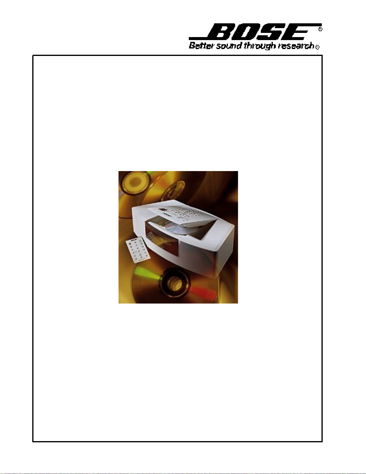
Bose® Wave® Radio/CD
100V/120V/230V/240V
PCB193325 and 252178
Click here to go to the
table of Contents
Service Manual
Part Number 250443 REV. 05
Page 2

Click here for a BWR/CD product Image
Contents
Safety Information.............................................................................................................................2
Electrostatic Discharge Sensitive (ESDS) ......................................................................................2
Specifications ................................................................................................................................ 3-6
Theory of Operation .................................................................................................................... 7-11
Disassembly/Assembly Procedures ........................................................................................ 12-13
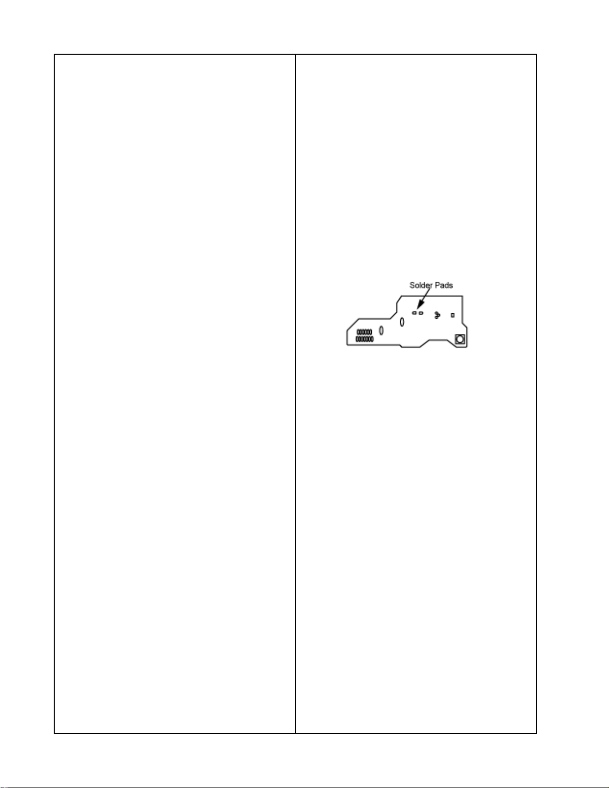
Figure 1. APC PCB, ESD Solder Points ............................................................................................12
Test Procedures ........................................................................................................................ 14-17
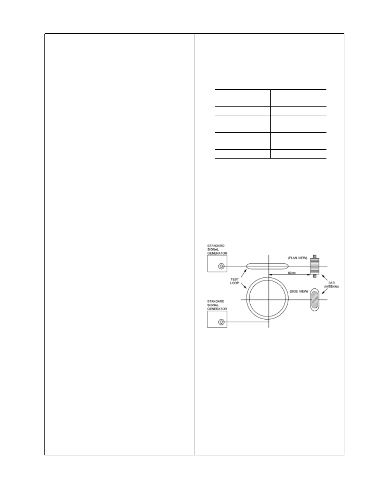
Figure 2. AM Test Setup ....................................................................................................................15
Part List Notes .................................................................................................................................18
Main Assembly Part List .................................................................................................................19
Figure 3. System Exploded View ....................................................................................................... 20
Electrical Part List ..................................................................................................................... 21-36
Packaging Part List .........................................................................................................................37
Figure 4. Packaging View .................................................................................................................. 37
Abbreviated Operating Instructions ..............................................................................................38
Figure 5. Keyboard Schematic Diagram ............................................................................................ 39
Manual Overview
The BWR/CD was originally manufactured with PCB 193325, PCB assembly 193321-1. Later
version units were manufactured with PCB 252178, PCB assembly 252441-1. Service information
for both versions is included in this manual.
®
CAUTION: THE BOSE
ABLE PARTS. TO PREVENT WARRANTY INFRACTIONS, REFER SERVICING TO WARRANTY SERVICE STATIONS OR FACTORY SERVICE.
W AVE® RADIO/CD CONTAINS NO USER SERVICE-
The Bose
WARRANTY INFORMATION
wave radio/CD is covered by a limited 1-year transferable warranty
1
Page 3

SAFETY INFORMATION
1. Parts that have special safety characteristics are identified by the symbol on schematics or
by special notes in the part lists. Use only replacement parts that have critical characteristics recommended by the manufacturer.
2. Make leakage current or resistance measurements to determine that exposed parts are acceptably insulated from the supply circuit before returning the unit to the customer. Use the following
checks to perform these measurements:
A. Leakage Current Hot Check-With the unit completely reassembled, plug the AC line cord
directly into a 120V AC outlet. (Do not use an isolation transformer during this test.) Use a leakage
current tester or a metering system that complies with American National Standards Institute (ANSI)
C101.1 “Leakage Current for Appliances” and Underwriters Laboratories (UL) 1492 (71). With the
unit AC switch first in the ON position and then in OFF position, measure from a known earth
ground (metal water pipe, conduit, etc.) to all exposed metal parts of the unit (antennas, handle
bracket, metal cabinet, screwhead, metallic overlays, control shafts, etc.), especially any exposed
metal parts that offer an electrical return path to the chassis. Any current measured must not exceed
0.5 milliamp. Reverse the unit power cord plug in the outlet and repeat test. ANY MEASUREMENTS
NOT WITHIN THE LIMITS SPECIFIED HEREIN INDICATE A POTENTIAL SHOCK HAZARD THAT
MUST BE ELIMINATED BEFORE RETURNING THE UNIT TO THE CUSTOMER.
B. Insulation Resistance Test Cold Check-(1) Unplug the power supply and connect a jumper wire
between the two prongs of the plug. (2) Turn on the power switch of the unit. (3) Measure the resistance with an ohmmeter between the jumped AC plug and each exposed metallic cabinet part on
the unit. When the exposed metallic part has a return path to the chassis, the reading should be
between 1 and 5.2 Meg ohms. When there is no return path to the chassis, the reading must be
“infinite”. If it is not within the limits specified, there is the possibility of a shock hazard, and the unit
must be repaired and rechecked before it is returned to the customer.
ELECTROSTATIC DISCHARGE SENSITIVE (ESDS)
DEVICE HANDLING
This unit contains ESDS devices. We recommend the following precautions when repairing, replacing or transporting ESDS devices:
• Perform work at an electrically grounded work station.
• Wear wrist straps that connect to the station or heel straps that connect to conductive floor mats.
• Avoid touching the leads or contacts of ESDS devices or PC boards even if properly grounded.
Handle boards by the edges only.
• Transport or store ESDS devices in ESD protective bags, bins, or totes. Do not insert unprotected
devices into materials such as plastic, polystyrene foam, clear plastic bags, bubble wrap or plastic
trays.
2
Page 4
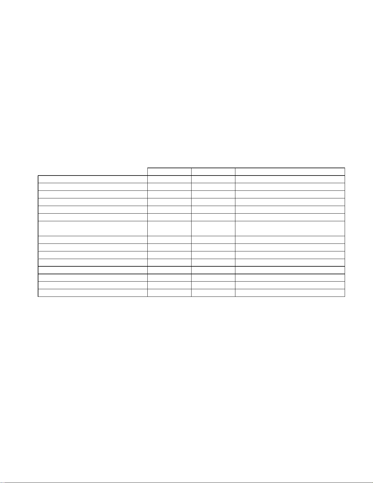
SPECIFICATIONS
Physical Description
Dimensions:
Weight:
Enclosure:
Input Line Voltage:
Power Consumption:
Maximum output level 2.0 V ±2.0 dB 0 dB
THD + noise .03% .08% 1 kHz, -6 dB
Signal to Noise Ratio 95 dB 90 dB A-weighted
Channel reparation 80 dB 70 dB 1 kHz
Frequency response ±.5 dB ±1.0 dB 20 Hz-15 kHz
Low-level linearity error 5.0 dB 10.0 dB -90 dB
De-emphasis 5 kHz
Dynamic range 95 dB 90 dB 1 kHz, -60 dB, IEC-A, 20 kHz, LPF
Defect tracking (interruption) 1.0 mm .8 mm ABEX test disc TCD-725R
Defect tracking (black dot) 1.0 mm .8 mm ABEX test disc TCD-725R
Defect tracking (scratch) 1.6 mm 1.0 mm ABEX test disc TCD-721R
Defect tracking (finger print) 75 µm 65 µm ABEX test disc TCD-725R
Defect tracking (warped disc) 1.0 mm .7 mm ABEX test disc TCD-732RA
Defect tracking (eccentric disc) 280 µm 210 µm ABEX test disc TCD-714R
Cueing time 2 sec 3 sec Phillips TS4, tracks 1-15
14" W x 8.5" D x 4.375" H (35.6 x 21.6 x 11.1) cm
7.4 lb (3.4 kg)
Injection molded thermal plastic
Power Specifications
120V, 60 Hz, 50W
¡
8 W with unit switched off
¡
50 W with CD player on, maximum output
CD Specifications
Nominal Limit Conditions
-4.53 dB
16 kHz
-9.04 dB
±2.0 dB
±2.0 dB
FM Antenna:
Tuning range:
De-emphasis:
Frequency steps:
Tuner Specifications
FM
75 Ohm external antenna connection, line cord
functions as an FM antenna
US: 87.7 MHz-107.9 MHz
Euro: 87.7 MHz-108.0 MHz
Japan: 76.0 MHz-90.0 MHz
US: 75 sec.
Euro: 50 sec.
Japan: 50 sec.
US: 200 kHz
Euro: 50 kHz
Japan: 100 kHz
3
Page 5
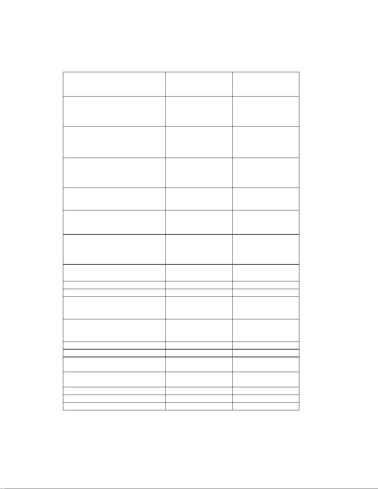
SPECIFICATIONS
FM Specification
(continued)
FM specifications per IHF-T-200, unless other wise noted. Measurement conditions, unless otherwise noted: RF input
frequency 98.1 MHz, audio frequency 1 kHz, RF input level 65 dBf, 75 kHz Deviation: Mono ±75 kHz, stereo ±67.5 kHz,
±7.5 kHz pilot. The performance specifications listed below apply across the entire FM band.
Specification Parameter Nominal Limit
(Ambient/
Environmental1)
Sensitivity usable (C1 removed)
US:
Euro:
Japan:
Sensitivity usable (C1 present3)
US:
Euro:
Japan:
Stereo (50 dB quieting)
US:
Euro:
Japan:
Signal to noise ratio at 65 dBf
Mono:
Stereo:
Signal to hum ratio at 65 dBf
Harmonic distortion (1 kHz) at 65
dBf
Harmonic distortion (1 kHz) at
65 dBf with ARI
Capture ratio 3.0 dB 4.0 dB
AM rejection at 45 dBf 55 dBf 50 dBf
Adjacent channel selectivity
Alternate channel selectivity
Image rejection 46 dB 40 dB
RF intermodulation 60 dB 55 dB
Subcarrier product rejection at
65 dBf
Frequency response
30 Hz-15 kHz
Stereo channel separation at 1 kHz 30 dB 20 dB
Auto stop level (seek) 32 dBf 5/10 dBf
Mono/stereo threshold 42 dBf 5/10 dB
4
2
Mono:
Stereo:
Mono:
Stereo:
US:
Euro:
US:
Euro:
Table notes:
1: Environmental limits apply from =10 to +40C
2: Signal to hum ratio is defined as the ratio of signal to hum and its harmonics
3: To measure usable sensitivity with C1 present, configure power cord to run straight back from the unit for one foot and
then straight downward for the remainder of the power cord’s length. Use an EMI filter or other method to provide RF
isolation at the wall outlet.
4: Use the standard European Broadcast Union ARI signal with 5 kHz signal on. DK signal on and BK signal code=F
13 dBf
14 dBf
13 dBf
15 dBf
16 dBf
15 dBf
43 dBf
45 dBf
43 dBf
70 dBf
65 dBf
80 dBf
80 dBf
.3%
.6%
.6% 1.5%
15 dB
15 dB
65 dB
65 dB
45 dB 40 dB
1.0 dB 3.0 dB
17/23 dBf
19/25 dBf
17/23 dBf
19/25 dBf
21/27 dBf
19/25 dBf
48 dBf
50 dBf
48 dBf
65/60 dBf
60/55 dBf
75 dBf
75 dBf
.6/2.0%
1.0/2.0%
10 dB
10 dB
60 dB
60 dB
4
Page 6
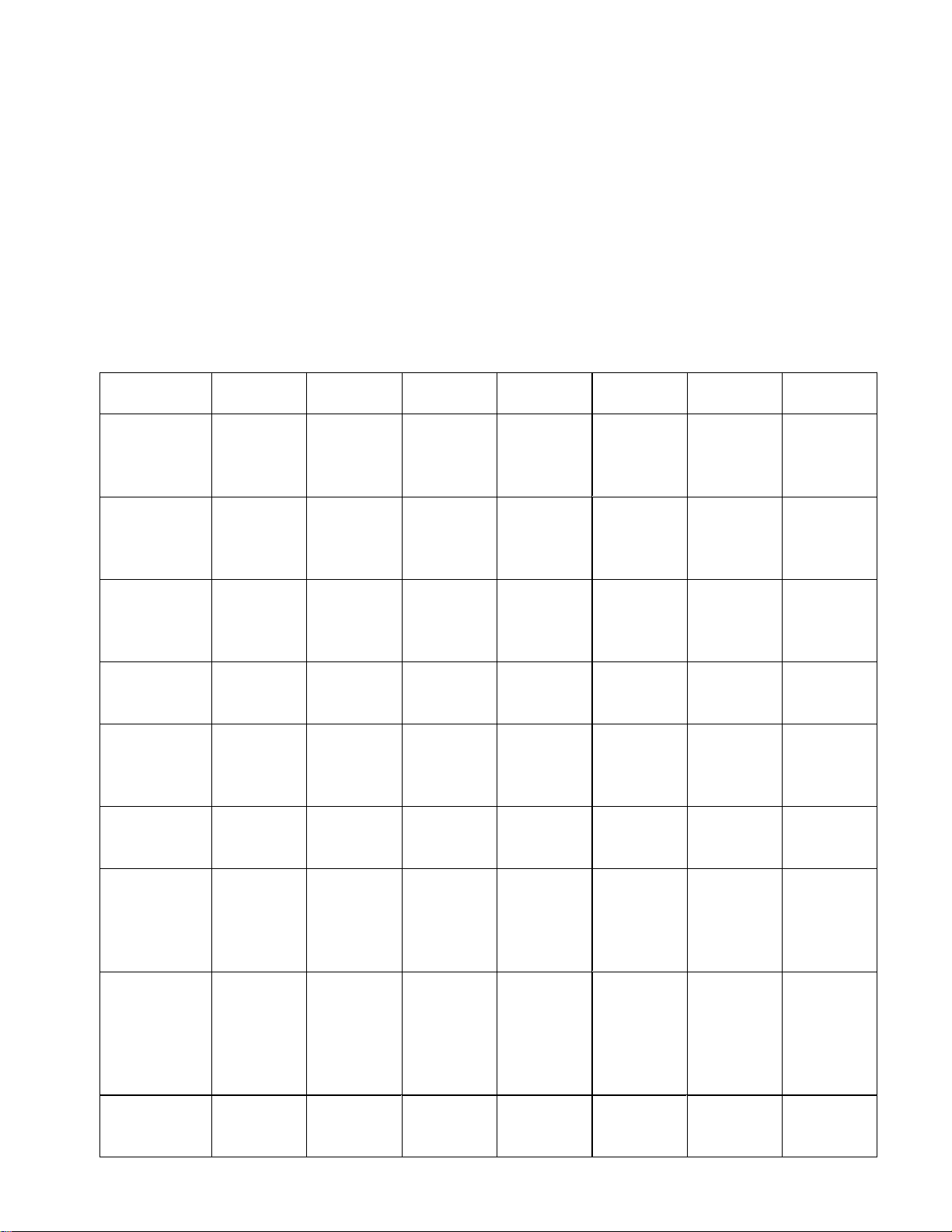
SPECIFICATIONS
(continued)
AM
AM Antenna:
Channel spacing:
Band Limits:
Test
Parameter
Usable
sensitivity,
dB V/m, 200
Hz HPF
Adjacent
channel
selectivity,
dB
Alternate
channel
selectivity,
dB
Image
rejection
ratio, dB
Signal to
noise, dB,
at 100 dB
V/M
Distortion,
%, at 100 dB
V/M
Frequency
response,
dB, at 50 Hz,
1.8 kHz, at
100 dB V/M
Conducted
susceptibility
diff. mode,
dB, min
Com. mode,
dB, min
Auto stop
level, dB
V/M
Internal bar antenna, turn unit to optimize AM
reception
US: 10 kHz
Euro: 9 kHz
Japan: 9 kHz
US: 520 kHz-1710 kHz
Euro: 522 kHz-1611 kHz
Japan: 522 kHz-1629 kHz
530-550 kHz 560-590 kHz 600-700 kHz 710-950 kHz 960-1400
kHz
55/63/69
nominal/limit/
environmental
42/37
nominal/limit
55/50
nominal/limit
45/40
nominal/limit
50/40/35
nominal/limit/
environmental
.8/1.4/2
nominal/limit/
environmental
-3/-6
nominal/limit
20
25
56 56 56 56 56 56 56
54/59/65
nominal/limit/
environmental
42/37
nominal/limit
55/50
nominal/limit
45/40
nominal/limit
50/40/35
nominal/limit/
environmental
.8/1.4/2
nominal/limit/
environmental
-3/-6
nominal/limit
20
25
51/56/62
nominal/limit/
environmental
40/35
nominal/limit
55/50
nominal/limit
45/40
nominal/limit
50/40/35
nominal/limit/
environmental
.8/1.4/2
nominal/limit/
environmental
-3/-6
nominal/limit
20
25
50/55/61
nominal/limit/
environmental
35/30
nominal/limit
55/50
nominal/limit
45/40
nominal/limit
50/40/35
nominal/limit/
environmental
.8/1.4/2
nominal/limit/
environmental
-3/-6
nominal/limit
20
25
49/54/60
nominal/limit/
environmental
35/30
nominal/limit
55/50
nominal/limit
42/37
nominal/limit
50/40/35
nominal/limit/
environmental
.8/1.4/2
nominal/limit/
environmental
-3/-6
nominal/limit
20
25
1410-1610
kHz
48/53/59
nominal/limit/
environmental
35/30
nominal/limit
55/50
nominal/limit
35/30
nominal/limit
50/40/35
nominal/limit/
environmental
.8/1.4/2
nominal/limit/
environmental
-3/-6
nominal/limit
20
25
1620-1710
kHz
50/55/61
nominal/limit/
environmental
35/30
nominal/limit
55/50
nominal/limit
35/30
nominal/limit
50/40/35
nominal/limit/
environmental
.8/1.4/2
nominal/limit/
environmental
-3/-6
nominal/limit
20
25
5
Page 7

SPECIFICATIONS
(continued)
Audio
THD at amplifier
output:
THD at line output: <.2% at 1 kHz, 2.0 Vrms AUX input
Auxiliary input
sensitivity:
Auxiliary input
impedance:
Speaker output
noise:
Signal to noise at
line output:
Volume control
increments:
Volume control
range:
<.2% at 1 kHz, at 80% of maximum
output
400 mVrms at 1 kHz for full output. 2.0
Vrms maximum auxiliary input
20 k Ohms
500 µVrms, maximum volume, inputs
shorted
85 dB
1.25 dB
78.75 dB at 1 kHz
Miscellaneous
Battery backup: 9 V, lasts up to 24 hours (alarm only)
6
Page 8

THEORY OF OPERATION
Note: All reference designators between 0 and 50 refer to components in the power supply and
power amplifier on sheet 1 of the schematic. All reference designators between 200 and 299 refer to
components in the voltage regulation section on sheet 2 of the schematic. All reference designators
between 300 and 399 refer to components in the tuner section on sheet 3 of the schematic. All 400
series components are located on the Micro Controller PCB, shown on sheet 4 of the schematic. All
reference designators between 500 and 599 refer to components in the CD section on sheet 5 of
the schematic. All reference designators between 600 and 699 refer to components in the audio
section on sheet 5 of the schematic.
1.0 Overview
The Wave® Radio/CD is an AM/FM tuner, single disk CD player, and powered speaker system. In
addition to the internal sources, external devices such as a tape deck can be connected through the
unit’s AUX input. An infrared (IR) remote control can be used to control the unit.
2.0 Power Supply Electronics
AC mains are connected through the line cord attached to the polarized jack J1. The neutral wire of
the line cord is used as an FM antenna coupled by C1. L1 and L2 provide isolation between the FM
RF input and the transformer T1. A slow acting fuse F1 is connected between J1 and the non-
polarized jack J2 to protect against faults.
Transformer T1 is a round core (R-core) transformer with one primary winding (unique for different
AC mains voltage requirements) and three secondary windings. The primary has a series thermal
fuse to protect against overload and faults. Two of the three secondary windings have center taps.
Polarized jack J3 ensures the correct connection of the pins from T1.
The first secondary winding of T1 provides the main audio power V and the CD motor power
VMOTOR. Bridge rectifier BR1 serves dual-purposes: it full wave rectifies the AC from two ends of
the first secondary (without the center tap) (creating V when filtered by C6; part of it also rectifies
through the center tap creating VMOTOR (about V/2)) when filtered by C16. The quiescent voltages
of V and VMOTOR are about 15VDC and 7.5VDC, respectively. V provides power to the uC elec-
tronics (+5V) and the CD electronics (+5VCD). A 9V battery connected to J200 also provides
backup power for the uC in case of a power outage. The switching between V and BAT+ is auto-
matic through D207. +5V is regulated by U202, a voltage regulator with low dropout voltage and low
quiescent current characteristics. Such characteristics are necessary to extend the battery life.
+5VCD is regulated by U203. R212 is a dissipating element for U203.
The second secondary winding of T1 provides power to the audio and RF electronics: a positive
voltage rectified by D201 and filtered by C205; and a negative voltage rectified by D200 and filtered
by C202. The positive voltage is regulated by U201 to generate +10V for the audio electronics. R208
is a dissipating element for U201. The uC controls +10V and +5VCD through Q207, D202, Q206
and Q208. In the off mode and battery backup mode the uC releases TURNON, turning off Q206
and Q208 and consequently +10V and +5VCD. In any other mode the uC asserts TURNON. The
negative voltage is regulated by U200 to provide -15V for the audio electronics. A reference voltage
of -20.6V is created by the 5.6V zener diode ZR200 and R201 between -15V and the negative
voltage. This -20.6V reference is buffered by Q202 to make -20V for the VFD electronics. The VFD
“center tap voltage” CT is generated from -15V by Q201. The uC controls the brightness of the VFD
partly by changing the CT voltage. It does so through AUD-DATA, Q210 and the resistor network
R231 and R232. AUD-DATA from the uC is multiplexed and filtered by R230 and capacitor C231.
Normally in a bright environment, AUD-DATA is filtered to be high so Q210 is turned off. The base of
7
Page 9

THEORY OF OPERATION
Q201 is at the same voltage as -15V. Consequently CT is at about -14.4V. In a dark environment,
AUD-DATA is filtered to be low so Q210 is turned on. The presence of +5V at the resistor network
changes the voltage at the base of Q201. CT is increased to about -9V, consequently reducing the
display brightness.
The third secondary winding of T1 provides AC power to the VFD filaments. It is nominally 5.3VAC.
The center tap is connected to CT so that the VFD filaments are negatively biased.
R200 is used to protect Q201 at power up. R207, R211 and R214 are fusible resistors protecting
against faults.
A line frequency signal (60 Hz) is generated from the secondary MAIN. MAIN is filtered by R205
and C215, clamped by D206, and buffered by Q200. 60 Hz (60 Hz or 50 Hz depending on the AC
mains) is used by the uC to keep time and to detect a power failure.
3. Control Electronics
The embedded micro-controller (uC) used in this system is a Toshiba TMP87xx14F, where the xx
digits define whether it is an OTP or a masked part. The main system power supply and the battery
are connected to a low dropout low quiescent current regulator through D207; when the main power
supply drops below the battery level, the battery will drive the uC. U403 is an automatic reset chip
that monitors the 5 volts at the uC and will pull pin 29 of the uC (RESET) low if the voltage drops
below 4.75 volts; it also supplies the power-on reset pulse. CF401 is an 8.00 MHz ceramic resonator
with built in capacitors.
U401 is an Electrically Erasable Read Only Memory that is used to store presets, AM and FM stop
levels, the stereo threshold level and other pieces of data. All of the series resistors and shunting
capacitors used on the signal lines leaving the uC are helping control conducted RF emissions from
the uC. D401 is a light sensor that in combination with R420 provides a voltage related to the light
level in the room. This voltage is read by the analog to digital converter at bit 7 of port 6 and is used
in the VFD dimming algorithm. Q401 is the infrared detector that works with the IR remote. The
series resistors and shunting caps tied to the pins of the VFD are used to control RF emissions. The
shunting resistors connected to six of the VFD control lines are used to help discharge the VFD
lines when those particular segments or grids are to be turned off. Q405 and Q406 increase the
current drive for two grids.
KEYIN1 through KEYIN4 and KEYOUT1 through KEYOUT6 are routed to the button board through
J403 and form a button matrix. Normally, the uC holds the KEYOUT lines low and pins 59 through
62 of the uC, which correspond to the KEYIN lines, will be pulled low through R468, R469, R470
and R430. The uC has internal 80k pull downs to -20 Volts on pins 59 through 62, so the voltage
there will actually be less than 0. The transistors Q400, Q402, Q403 and Q404 are used for level
shifting and current gain to overcome the resistance of the carbon ink button board. When a button
is pressed, a KEYOUT line will pull current through the base of the corresponding KEYIN transistor
and drive one of the pins on the uC high. The uC will now begin scanning the KEYOUT lines by
pulling each line individually high one at a time. This way, when the KEYIN signal disappears the uC
will know the corresponding KEYOUT line and which button in the matrix is pressed. The uC can
now execute the desired command.
8
Page 10

THEORY OF OPERATION
4.0 Audio Electronics
The two internal sources (CD and tuner) and the AUX input are routed to the audio multiplexer/
volume control chip U605. U605 selects one of the three inputs and routes the signal to pins 7 and
17 (right and left). These two signals are AC coupled to J600 as Line Outputs. Q602 and Q603
buffer a signal (BUZZER) from the uC that is summed with the left channel for use as an alarm. The
left and right signals then pass through matching EQ sections using R655, R656, C645, C646 and
R660, R657, C665, C666. These sections normally provide bass cut at loud volume settings. These
EQ sections increase the deep bass for lower volume settings. This is the dynamic EQ for the
product. The final stage of U605 is the volume control. U605 provides 80 dB of attenuation in 64
steps of 1.25 dB. The variable level signal is output on pins 24 and 25.
The audio signal is then split into two paths. The right and left signals are routed through U600 and
one quarter of U601, which provide active filtering for the left (full range) speaker output. The right
signal is also routed through three-quarters of U601 which provides active filtering for the right
(Twiddler
The two audio signals are fed to the power amplifier U1. U1 is a bridged stereo power amp used for
the right and left channels. The U1 outputs are routed through J5 and J6 to the left and right drivers
respectively. U1 also contains a clip detector that is output on pin 4. This signal (COMP) controls the
bias current of U603. When the amplifier is clipping, the bias current of U603 is increased. The
change in gain of U603 reduces the bass frequency response of the left channel EQ. This is the
compressor for the product.
TM
) speaker output.
Q4 is an amplifier that is connected to the Twiddler. It amplifies the signal BUZZER only when the
unit is not powered. The power for this comes from the nine-volt battery.
5. Tuner Electronics
There are two major ICs in the tuner section: U300, an AM/FM radio chip with a built in stereo de-
multiplexer, and U301, a Phase Lock Loop (PLL) chip. The main system embedded controller (µC)
talks to the PLL chip using signals AUD-DATA, PLL-DATA, AUD-CLK and PLL-CE. The µC controls
whether the tuner is in AM or FM mode by forcing pin 8 of the PLL either high or low; a low puts
U300 in AM mode and disables power to the FM-TUNER and a high puts U300 into FM mode and
turns on power to the FM-Tuner via Q300 and Q301.
In FM mode the frequency of the local oscillator (LO) located in the FM-TUNER is adjusted by the
signal FM_TV which is applied to pin 5 of the FM-TUNER. The LO is then output on pin 8 and
routed back to U301 via C338. The PLL then compares the scaled frequency/phase of the LO
against a reference which is a division of the 7.2 MHz oscillator composed of U301, C341, C342
and CF303. The result of this comparison determines the density and polarity of the phase pulses
which are output on pin 16 of U301. The phase pulses then go into the loop filter composed of a
MOSFET inside of U301 (Ain and Aout) and the discrete components attached to pins 16, 17 and
18. The loop filter integrates the phase pulses to form the DC control voltage FM_TV thus complet-
ing the LO control loop.
Inside the FM-TUNER, the LO is mixed with the RF signal, coming from the F-Connector J300 or off
of the AC line cord neutral wire via C1, to produce an IF signal centered at 10.7 MHz that is output
on pin 7. The IF signal then passes through ceramic filter CF300, the common emitter amp contain-
ing Q303, CF301 and is then routed into U300. Inside the chip the IF signal is limited and detected.
The resonant LC circuit on pin 9 is part of the detector circuit. After detection, the stereo signal is
9
Page 11

THEORY OF OPERATION
then de-multiplexed inside the chip and the stereo channels are output onto pins 16 and 17. The
ceramic resonator CF302 is used by the stereo de-multiplexer’s VCO. C321, C320 and R315 form
the loop filter for the de-multiplexer’s PLL. The left and right channel signals are then routed through
the 19 kHz pilot reject filters composed of T303 and T304. The µC makes stop and stereo threshold
decisions based on the level of the S-METER signal which is read by the analog to digital converter
in the µC. The µC forces the radio into mono mode by telling U301 to force its pin 9 low.
For AM, the Local Oscillator is composed of the LC resonant circuit, which is half of D304 and T302,
and an amplifier in U300. The AM LO signal comes out of pin 30 of U300 and is fed into U301 via
R330 and C337. The PLL chip compares the scaled LO frequency against a division of the 7.2 MHz
oscillator and outputs the appropriate phase pulses from pin 16 into the loop filter. The tuning voltage comes out of the loop filter through R309 and appears across pins 1 and 2 of the varactor diode
to complete the AM LO control loop.
The inductance of the AM Bar Antenna at pins 3 and 4 form a parallel resonance with the capacitance between pins 3 and 2 of the varactor diode producing frequency selectivity at the antenna.
The RF at pin 1 of the antenna is routed into pin 27 of U300. The input circuitry at pin 27 is biased to
3.6 volts (Vreg) through R308 and the coil wound between pins 1 and 2 on the antenna. Inside the
chip, the RF is amplified and mixed down to an IF (intermediate frequency) of 450 kHz. The IF is
output on U300 pin 2 and routed to the IF filtering in T301. The filtered IF then enters U300 at pin 5
and passed through audio detection in the chip. The audio is then output onto pins 16 and 17.
6.0 CD Electronics
The CD circuitry consists of four major sections: the analog signal processor (ASP) U500, digital
signal processor (DSP) U501, power driver U502 and the CD mechanism. U500 contains the RF
amplifier and servo control circuits. U501 performs EFM demodulation, CIRC decoding, digital
filtering, D to A conversion and low-pass filtering. It also extracts the subcode Q data (track #, time,
etc.).
U500 receives its input signal (through J500) from the mechanism’s photo diode pickup. The inputs
A, B, C and D are added together and amplified. The RF amplifier output appears on RFSM (U500,
pin 41). This signal is the familiar eye pattern. This signal is sent to EFMIN on U501 pin 10 where it
is sliced for EFM demodulation. The sliced output appears on EFMO (U501 pin 9). A low-passed
version of this signal appears on SLC (U500 pin 43) and is used as a DC bias for the RFSM signal.
The RFSM signal is peak detected and compared to a reference to determine if there is a signal
being received from the disc. The output appears on DRF (U500 pin 54). This signal is used by the
µC to determine if the lens is in focus. The envelope of the RFSM signal is used to determine when
the laser crosses a track boundary during track access. The HFL signal (U500 pin 37) conveys this
information to U501.
The B+D signal (FIN2) is subtracted from the A+C signal (FIN1). This produces the focus error
signal FE (U500 pin 20). This signal is amplified and filtered by the focus servo amplifier within
U500. It then appears as an output FD (U500 pin 16). The FD signal is fed to U502. U502 generates
a bridged output which is used to actuate the focus coil (J500 pins 10 and 13).
The E and F signals are buffered by U500. E is then subtracted from F and this difference is the
track error signal TE (U500 pin 7). TE is used by both the anti-shock circuit and the tracking servo.
TE is filtered at the SCI input (U500 pin 9) to determine if the system has had a shock. If this occurs,
U500 increases the track gain internally to compensate for the shock. The TE signal is amplified and
filtered by the tracking servo amplifier within U500. It then appears as an output TO (U500 pin 15).
10
Page 12

THEORY OF OPERATION
The TO signal is fed to U502. U502 generates a bridged output which is used to actuate the track
coil (J500 pins 11 and 12).
The TO signal is also used as an input to the sled servo. This signal is filtered and fed to the sled
servo amplifier on SLEQ (U500 pin 28). This signal is amplified and added to the SLED signals from
the µC. The sum appears on SLD (U500 pin 29), which is fed to U502. U502 generates a bridged
output to drive the sled motor (J502 pins 5 and 6).
The Constant Linear Velocity (CLV) servo is regulated by comparing the bit rate to a fixed reference
frequency in U501. The error signal appears at U501 pins 12 and 13 (CLV+ and CLV-). These
signals are subtracted and the difference appears on SP (U500 pin 23). The SP signal is filtered and
amplified. The signal then appears at the output on SPD (U500 pin 27). SPD is fed to U502. U502
generates a complimentary output which drives the spin motor (J502 pins 1 and 2).
U500 regulates the laser power by monitoring the LDS input (J500 pin 8). This signal is compared to
a reference to generate the proper drive signal on LDD (U500 pin 62). This signal is buffered by
Q500. The Q500 output is amplified by Q501. Q501 drives the laser diode output LD (J500 pin 6).
U500’s main DC reference voltage is VREF (U500 pin 58). This voltage is nominally 2.5V.
U500 receives servo control commands from the µC on the serial bus (U500 pins 51, 52 and 53).
These commands are used to start focus offset cancellation, track offset cancellation, E/F balance
adjustment, focus initialization, laser ON/OFF and 8/12 cm spindle gain.
The DSP clock is derived from a 16.9344 MHz crystal oscillator (CF500). U501 divides this clock by
four to generate a 4.2336 MHz signal that is output as the signal 4.2M (U501 pin 61). 4.2M is used
as a system clock by the ASP.
U501 receives servo control commands from the µC on the serial bus (U501 pins 57, 56 and 54).
These commands include track jump, focus start, disk motor start/stop, muting on/off and track
count. The tracking servo is controlled by the TOFF and TGL outputs (U501 pins 17 and 18). Track
jumps are created by signals on the JP+ and JP- lines (U501 pins 19 and 20). Track jump detection
is based on signals from U500 on the HFL and TES inputs. U501 removes the subcode Q data from
the bit stream and makes it available to the µC. The µC extracts track, time and table of contents
information from the subcode Q.
U501 receives its EFM input from U500 on EFMIN (pin 10). This signal is sliced, EFM demodulated
and CIRC decoded. The digital audio signal is passed through a 4x over-sampling digital filter, D/A
converter and low-pass filter. These outputs appear on RCHO and LCHO (U501 pins 40 and 37).
The audio signals are routed to U605.
11
Page 13
DISASSEMBLY/ASSEMBLY PROCEDURES
Note: The numbers in parentheses refer to the
callouts in Figure 3.
1. Top Cover Removal
1.1 Remove the three screws (21) that secure
the top cover (6) to the base (9).
1.2 Insert a flat blade screwdriver into the two
locations shown in Figure 3. Apply force on the
flat blade screwdriver so that the grille is
moved outward and clears the two tabs located on the base.
1.3 Lift up on the top cover to remove it.
2. Top Cover Replacement
2.1 Lower the top cover (6) onto the base (9).
Make sure that the ribbon cable that connects
to the CD door (7) lays in the track to the left of
the CD mechanism (2).
Note: The light shield (4) can get caught on
the top cover. Make sure the light shield is
secured in place when replacing the top cover.
2.2 With the palms of your hands located on
the front corners of the top cover, press down
on the top cover until it snaps into place.
2.3 Replace the three screws (21) that secure
the top cover to the base.
3. Display PCB Removal
4.2 Lower the display PCB into the slots
located on the matrix assembly (8).
5. CD Mechanism Removal
5.1 Perform procedure 1.
5.2 Lift up the CD mechanism (2) and solder
the two points located on the CD mechanism’s
APC PCB. See Figure 1. This will prevent
static electricity damage to the CD mechanism.
5.3 Remove the cables from the CD
mechanism’s and lift out the CD mechanism.
Figure 1. APC PCB, ESD Solder Points
6. CD Mechanism Replacement
6.1 Attach the cables to the CD mechanism (2)
and remove the solder from the two points
indicated in Figure 1.
6.2 Lower the CD mechanism into the matrix
assembly (8) so that the cables are toward the
right speaker.
3.1 Perform procedure 1.
3.2 Lift up the display PCB (1).
3.3 Remove the ribbon cable that connects the
CD door (7) to the display PCB. Remove the
two ribbon cables that connect to the main
PCB. Lift out the display PCB.
Caution: If you remove the ribbon cable from
the CD door, you might have difficulties reconnecting the cable.
4. Display PCB Replacement
4.1 Replace the three ribbon cables that attach
to the display PCB (1).
7. Twiddler
7.1 Perform procedure 1.
7.2 Remove the four screws (18) that secure
the Twiddler/full-range driver (3, 4) to the
matrix assembly (8). Pull out the driver from
the matrix assembly and remove the soldered
wires from the driver.
12
TM
and Full-Range Driver Removal
Page 14
DISASSEMBLY/ASSEMBLY PROCEDURES
8. Twiddler
ment
8.1 Solder the red wire to the positive (+)
driver terminal and the black wire to the negative (-) driver terminal.
8.2 Align the driver (3, 4) into the matrix
assembly (8) so that the wires feed through
the channel on the top of the matrix assembly.
8.3 Replace the four screws (18) that secure
the driver to the matrix assembly.
9. Transformer Removal
9.1 Perform procedure 1 first.
9.2 Remove the three screws (17) that secure
the transformer (5) to the matrix assembly (8)
and lift up the transformer.
9.3 Remove the two wire connectors that
connect to the main PCB (1).
10. Transformer Replacement
10.1 Connect the two wire connectors to the
main PCB (1).
10.2 Lower the transformer (5) into the matrix
assembly and replace the three screws (17)
that secure the transformer to the matrix
assembly.
11. Main PCB removal
TM
and Full-Range Driver Replace-
11.5 Lift up the matrix assembly (8), discon-
nect the wire connectors from the main PCB
(1) and lift off the matrix assembly. Make a
note of the way the wires are dressed.
11.6 Disconnect the two ribbon cables that
connect the main PCB to the display PCB. Lift
up the main PCB.
12. Main PCB Replacement
12.1 Lower the main PCB (1) into the base.
Make sure that the nine-volt battery connector
is positioned properly in the battery compartment. Connect the ribbon cables from the
display PCB (1) to the main PCB.
12.2 Partly lower the matrix assembly (8) onto
the base and connect all the wire connectors
to the main PCB and then completely lower
the matrix assembly onto the base (9). Make
sure the AC line cord is inserted into the notch
on the base.
12.3 Replace the two screws on the left (17)
that secure the matrix assembly to the base
and the two screws (17) that secure the
transformer (5) to the matrix.
12.4 Lower the CD mechanism into the matrix
assembly (8) so that the cables are toward the
right speaker.
12.5 Lower the display PCB into the slots
located on the matrix assembly.
11.1 Perform procedure 1 first.
11.2 Remove the two lower screws (17) that
secure the transformer (5) to the matrix assembly (8). Remove the two screws (17) on
the left side that secure the matrix assembly to
the base (9).
11.3 Lift up the CD mechanism (2) and place it
off to the side.
11.4 Lift up the display PCB (1) and lay it down
in front of the unit.
13
Page 15
TEST PROCEDURES
General Test Setup Procedures
TM
Twiddler
W load to J6, pins 1 and 2. The Twiddler is the
right speaker, when viewed from the front of the
unit.
Full-range channel: Connect a 4 Ohm ± 1%, 25 W
load to J5, pins 1 and 2. The full range driver is
the left speaker, when viewed from the front of
the unit.
Adjust the volume to 64 unless otherwise noted.
Note: The door switch, located on the underside
of the door, needs to be closed for the function
buttons to work.
1. Mute Test
1.1 Apply a 1 Vrms, 1 kHz signal to the left and
right aux input.
1.2 Reference a dB meter to the Twiddler or
full-range output.
1.3 Press the mute button. The Twiddler or fullrange output should be <-55 dB.
2. Channel Separation
2.1 Apply a 1 Vrms, 1 kHz signal to the left
aux input and short the right aux input.
2.2 Reference a dB meter to the full-range
output.
2.3 Measure the Twiddler output. It should be
< -50 dB.
3. Compressor Distortion
3.1 Apply a 200 mVrms, 150 Hz signal to the
left and right aux input. Adjust the volume to
99.
channel: Connect an 8 Ohm ± 1%, 10
Audio Tests
4. DC Offset
4.1 Select the aux mode and short the left and
right aux input.
4.2 Measure the Twiddler and full-range
outputs. They should be >-150 mVDC and
< +150 mVDC.
5. Full Range Channel Output Noise
5.1 <1.0 mV, A-weighted, inputs shorted.
6. Full-Range Channel Reference Gain
6.1 Apply a 15 mVrms, 1 kHz signal to the left
and right aux input. Adjust the volume to 99.
6.2 Reference a dB meter to the applied
signal.
6.3 Measure the full-range output. It should be
+22.0 dB ± 2.2 dB.
7. Full-range Channel Frequency Response
7.1 Apply a 15 mVrms, 1 kHz signal to the left
and right aux input. Adjust the volume to 99.
7.2 Reference a dB meter to the full-range
output.
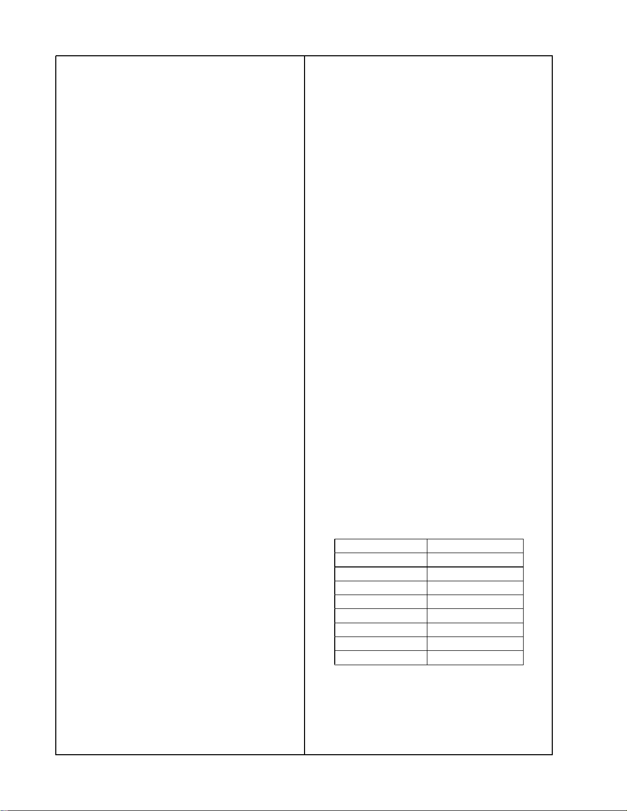
7.3 Measure the full-range output according to
the following table.
Frequency Output
50 Hz -8.3 ± 3.1 dB
90 Hz +16.5 ± 2.4 dB
300 Hz +4.8 dB ± 1.3 dB
500 Hz -1.2 ± 1.1 dB
1.0 kHz Reference
2.0 kHz +4.7 ± 1.0 dB
5.0 kHz +12.7 ± 1.0 dB
15 kHz +18.3 ± 2.2 dB
3.2 Measure the distortion at the full-range
output. It should be <5%.
14
Page 16
TEST PROCEDURES
8. Full-Range Channel Dynamic EQ Gain
8.1 Apply a 15 mVrms, 1 kHz signal to the left
and right aux input. Adjust the volume to 49.
Reference a dB meter to the full-range output.
8.2 Apply a 1.5 mVrms, 80 Hz signal to the left
and right input.
8.3 Measure the full-range output. It should be
+3.5 ± 1.0 dB.
9. Full-Range Channel Small Signal Distortion
at 0.1 W
9.1 Apply a 30 mVrms, 1 kHz signal to the left
and right aux input. Adjust the volume to 99.
9.2 Measure the full-range output. It should be
<0.5% THD.
10. Full-Range Channel Large Signal Distortion at 6 W.
10.1 Apply a 200 mVrms, 1 kHz signal to the
left and right aux input. Adjust the volume to 99.
13.2 Reference a dB meter to the Twiddler
output.
13.3 Measure the Twiddler output according to
the following table.
Frequency Output
200 Hz -15.6 ± 1.3 dB
400 Hz -4.6 ± 1.2 dB
550 Hz -1.8 ± 1.0 dB
1 kHz Reference
3 kHz -3.7 ± 1.0 dB
10 kHz +9.1 ± 1.0 dB
20 kHz +6.6 ± 1.5 dB
14. Twiddler Channel Small signal Distortion at
0.5 W
14.1 Apply a 130 mVrms, 1 kHz signal to the
left and right input. Adjust the volume to 99.
14.2 Measure the twiddler channel output. It
should be <0.1% THD.
10.2 Measure the full-range output. It should be
<0.2% THD.
TM
11. Twiddler
11.1 Measure the Twiddler channel output. It
should be <300 uV, A-weighted, inputs shorted.
12. Twiddler Channel Reference Gain
12.1 Apply a 50 mVrms, 1 kHz signal to the left
and right aux input. Adjust the volume to 99.
12.2 Reference a dB meter to the applied
signal.
12.3 Measure the Twiddler output. It should be
+20.5 ± 2.0 dB.
13. Twiddler Channel Frequency Response
13.1 Apply a 50 mVrms, 1 kHz signal to the left
and right input. Adjust the volume to 99.
Channel Output Noise
Figure 2. AM Test Setup
15. AM Tracking Alignment
15.1 Adjust the RF generator to 1500 kHz, 400 Hz,
30% AM modulation at a level of 70 dBuV/m at
the unit’s antenna.
15.2 Adjust C307 for peak audio output measured at the line output.
15.3 Adjust the RF generator to 600 kHz, 400 Hz,
30% AM modulation at a level of 70 dBuV/m at
the antenna.
15
Page 17
TEST PROCEDURES
15.4 Adjust T302 for peak audio output mea-
sured at the line output.
15.5 Adjust the RF generator to 1500 kHz, 400 Hz,
30% AM modulation at a level of 70 dBu/m at
the unit’s antenna.
15.6 Adjust C307 for peak audio output measure at the line output.
16. AM Sensitivity
16.1 Adjust the RF generator to 1080 kHz, 400
Hz, 30% AM modulation at a level of
53 dBuV/m at the unit’s antenna.
16.2 Reference a dB meter to the aux output.
16.3 Turn off the modulation and measure the
aux output. It should be < -20 dB.
17. AM Stop Level Adjustment
19.2 Reference a dB meter to the left line
output.
19.3 Switch the RF generator to right only
modulation. Verify that the left line output is
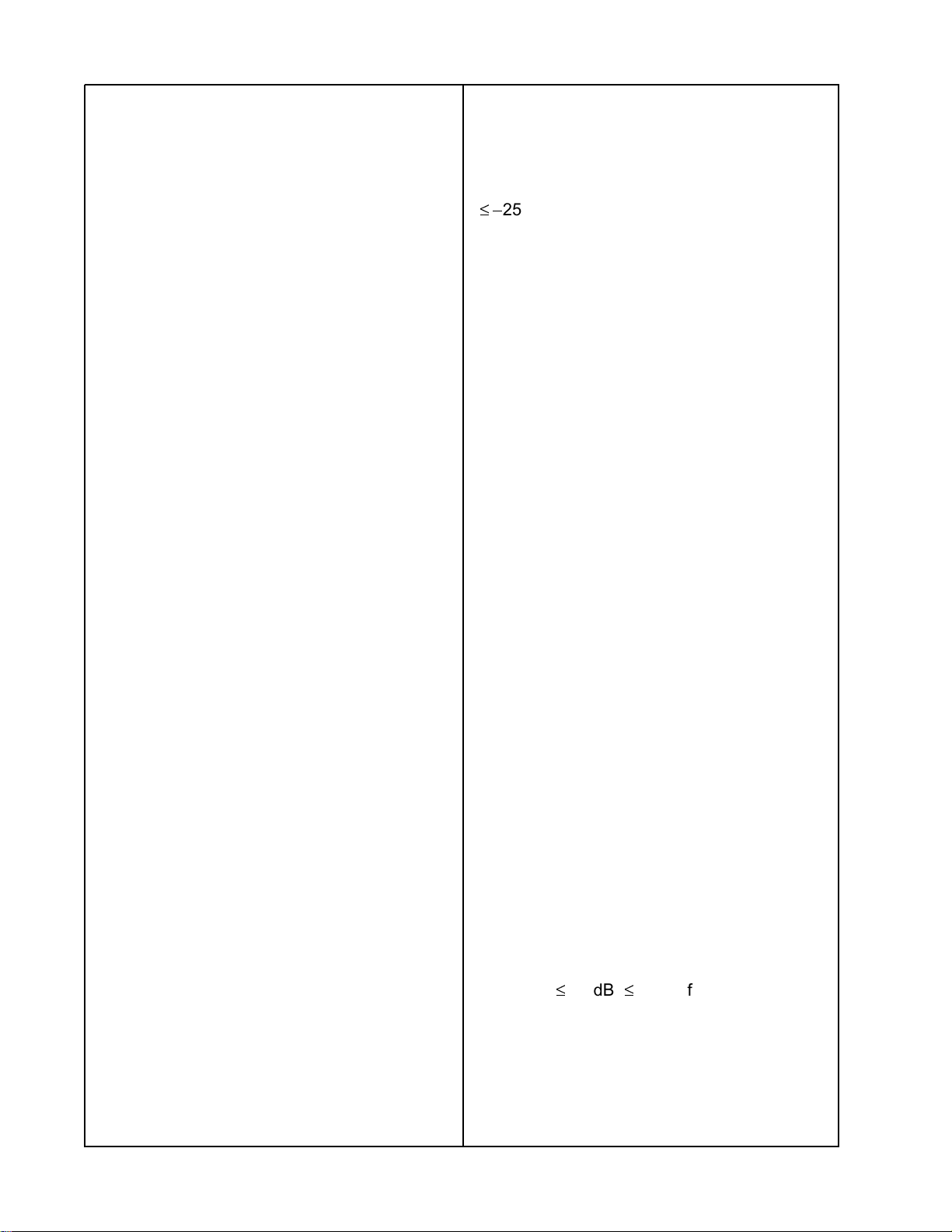
£ÿ-
25 dB.
20. FM Stop Level Adjustment
20.1 Adjust the RF generator to 98.1 MHz
(87.4 MHz for Japan), no modulation at a level
of 30 dBf into the antenna input.
20.2 Press the CD mode, FM and alarm 2
buttons at the same time to store the FM stop
level.
20.3 Adjust the RF generator to 98.9 MHz
(88.0 MHz for Japan), 1 kHz modulation, 75
kHz deviation at a level of 35 dBf into the
antenna input. Press the seek button and
verify the tuner stops at 98.9 MHz.
17.1 Adjust the RF generator to 1080 kHz, no
modulation at a level of 59 dBuV/m at the
unit’s antenna.
17.2 Press the CD mode, AM and Alarm 2
buttons at the same time to store the AM stop
level.
FM Tests
18. FM Detector Adjustment
18.1 Adjust the FM generator to 98.1 MHz
(87.4 MHz for Japan), 1 kHz modulation, pilot
off, 75 kHz deviation and at a level of 40 dBf
into the antenna input.
18.2 If the THD measured at the line output is
greater than .5%, adjust T300 until the THD is
less than .5%. Verify the line output is 560 mVrms
± 200 mVrms.
19. Stereo Separation
21. Stereo Threshold Adjustment
21.1 Adjust the RF generator to 98.1 MHz
(87.4 MHz for Japan), 10% pilot, 75 kHz
deviation at a level of 42 dBf into the antenna
input.
21.2 Press the CD mode, FM and CD stop
button at the same time to store the stereo
threshold.
22. FM Sensitivity
22.1 Adjust the RF generator to 98.1 MHz
(87.4 MHz), 1 kHz stereo L = R modulation,
10% pilot, 75 kHz deviation at a level of 48 dBf
into the antenna input. Reference a dB meter
to the line output.
22.2 Turn off the modulation and verify that the
line out is £ÿ50 dB (£ÿ45 dB for European
version).
19.1 Adjust the RF generator to 98.1 MHz
(87.4 MHz for Japan), 1 kHz stereo left only
modulation, 10% pilot, 75 kHz deviation at a
level of 65 dBf into the antenna input.
16
Page 18
TEST PROCEDURES
CD Tests
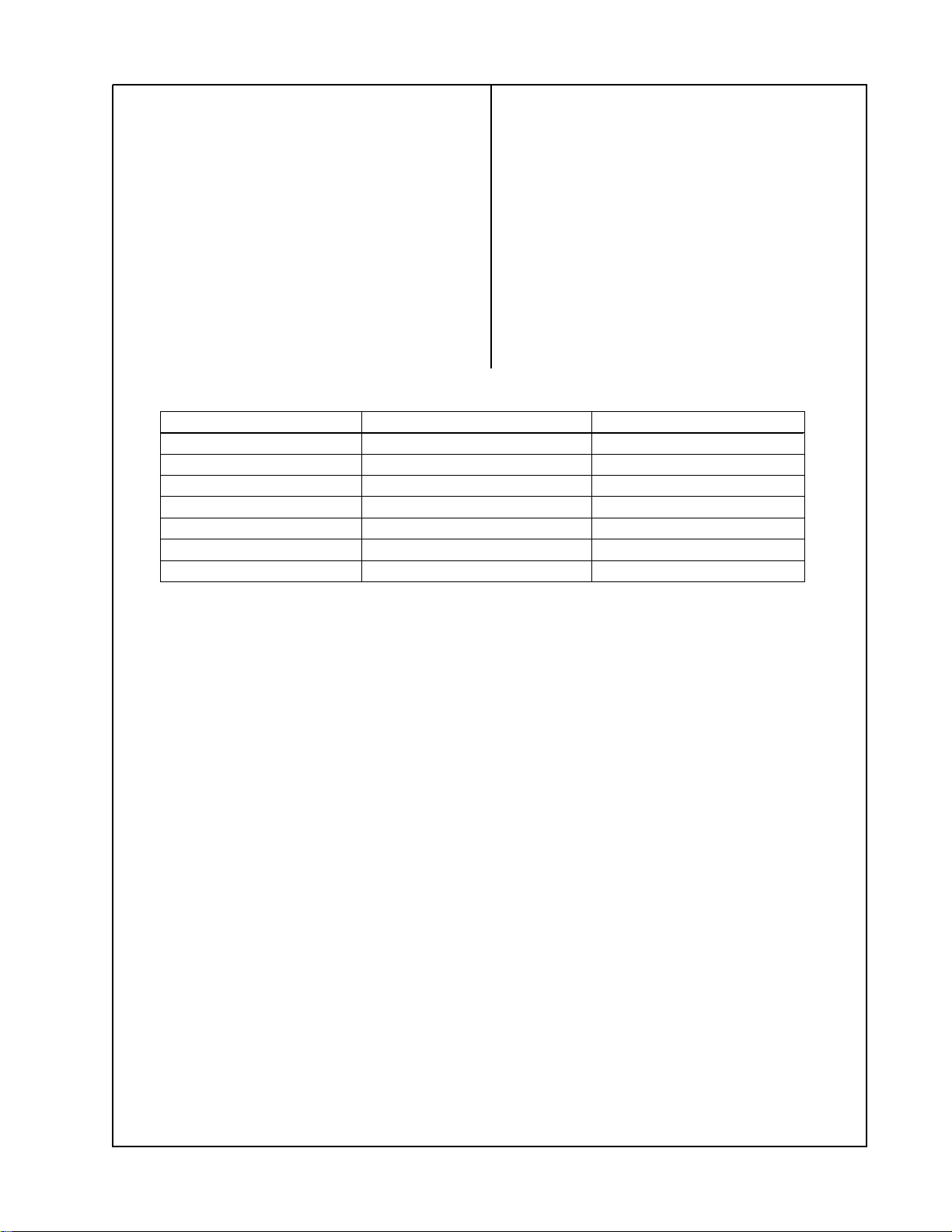
23. CD Performance Test
23.1 The BWR/CD should be able to play the
tests discs listed in the following table for the
amount of time stated without any audible
defects. There are no CD adjustments that can
be made to the BWR/CD. If the unit fails any of
these tests, replace the CD mechanism.
Test Disc Test Conditions
Void, 1.0 mm ABEX test disc TCD-725R Track 6, 6 sec.
Black dot, .8 mm ABEX test disc TCD-725R Track 9, 8 sec.
Finger print, 65 um ABEX test disc TCD-725R Track 13, 10 sec.
Warped disc, 1.0 mm ABEX test disc TCD-725RA First and last track, 6 sec.
Eccentric disc, 210 um ABEX test disc TCD-714R First and last track, 6 sec.
Cueing time, 2 sec. Phillips TS4, tracks 1-15 Skip first to last track
Long playability, 71’ 42 " ABEX test disc TCD-784 Last track, 6 sec.
17
Page 19

PART LIST NOTES
1. This part is not normally available from customer service. Approval from the Field Service Manager is required before ordering.
2. The individual parts are listed in the part list.
3. This part is critical for safety purposes. Failure to use a substitute replacement with the same
safety characteristics as the recommended replacement part might create shock, fire and/ or other
hazards.
4. This part is used on 120V version.
5. This part is used on 230V (EURO) version.
6. This part is used on 240V (AUS) version.
7. This part is used on 100V version.
8. This part is packed with the 100V version only. An antenna is not packed with the 120V version.
9. This part is used on PCB 193325, PCB assembly 193321-1
10. This part is used on PCB 252178, PCB assembly 252441-1
18
Page 20
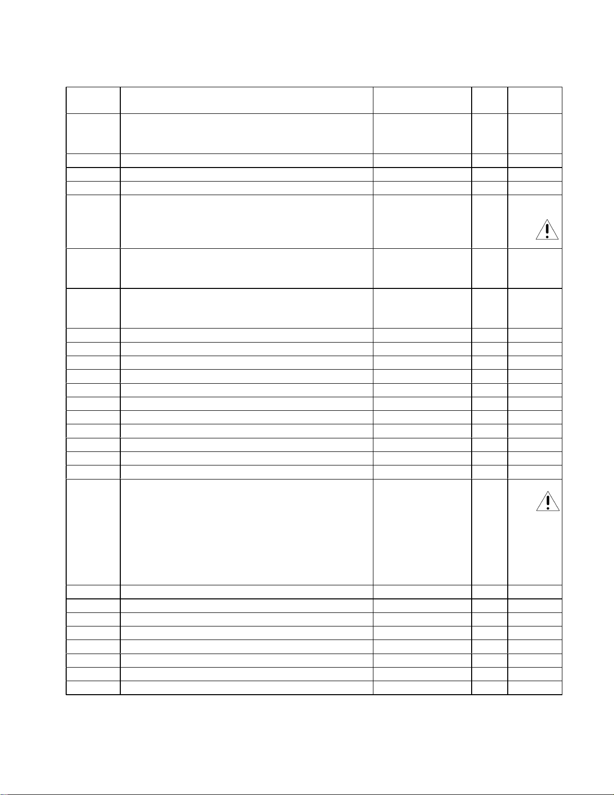
MAIN ASSEMBLY PART LIST
(refer to Figure 3)
Item
Number
1 PCB ASSEMBLY,120V
PCB ASSEMBLY, 220V/240V
PCB ASSEMBLY, 100V
2 CD MECHANISM, CD93V4M 193373 1
3 FULL-RANGE TWIDDLER®, W/HARNESS, LEFT 145588-002 1
4 TWIDDLER, W/HARNESS, RIGHT 148704-002 1
5 TRANSFORMER, R-CORE, 120V, 60HZ
TRANSFORMER, R-CORE, 230V, 50HZ
TRANSFORMER, R-CORE, 100V, 50HZ
6 TOP COVER IMPERIAL WHITE
TOP COVER, PLATINUM WHITE
TOP COVER, GRAPHITE
7 DOOR ASSEMBLY, IMPERIAL WHITE
DOOR ASSEMBLY GRAPHITE GRAY
DOOR ASSEMBLY, PLATINUM WHITE
8 MATRIX ASSEMBLY, BLACK 193376-011 1
9 PEDESTAL ASSEMBLY, BLACK 198614-001 1
10 LENS, GREEN 193392-001 1
11 SHIELD, LIGHT, CONTOURED 199608 1
12 CABLE, FLEX, 21 CONDUCTOR 193394-100 2
13 CABLE, FLEX, 13 CONDUCTOR 193374-100 1
14 HARNESS, 6 CONDUCTOR 193375-001 1
15 GROMMET, RUBBER, CUSHION, RED DOT 193382 1
16 GROMMET, RUBBER, CUSHION, WHITE DOT 193380 2
17 SCREW, TAPP, 8-11x.625, PAN, XRC/S 172672-10 6
18 SCREW, HILO, 6x.5, PAN, XREC 175972-08 8
19 LINE CORD, 120V, PLATINUM WHITE
LINE CORD, 120V, BLACK
LINE CORD, 230V, PLATINUM WHITE
LINE CORD, 230V, BLACK
LINE CORD, 240V, PLATINUM WHITE
LINE CORD, 240V, BLACK
LINE CORD, 100V, PLATINUM WHITE
LINE CORD, 100V, BLACK
20 CABLE, FLEX, 15 CONDUCTOR 193384-100 1
21 SCREW, TAP, 8-11X.625, PAN, XRC/SQ 193637-10 3
22 ARM, SPRING 193329 1
- BATTERY DOOR, BLACK 193409-001 1
- CLIP, DAMPER 193428 1
- GEAR, DAMPER, WHITE 146816-04 1
- SPRING, EXTENSION 193379 1
- FELT FOOT 193460-001 4
Description Part Number Qty. Note
252441-1 1 4
193372
250604
251780
198613-001
193391-010
193391-002
NOT AVAILABLE
198608-002
198608-010
193395-010
193395-001
193396-010
193396-001
251967-010
251967-001
193404-010
193404-001
5, 6
7
1 3, 4
3, 5, 6
3, 7
1
1
1 3, 4
3, 4
3, 5
3, 5
3, 6
3, 6
3, 7
3, 7
19
Page 21
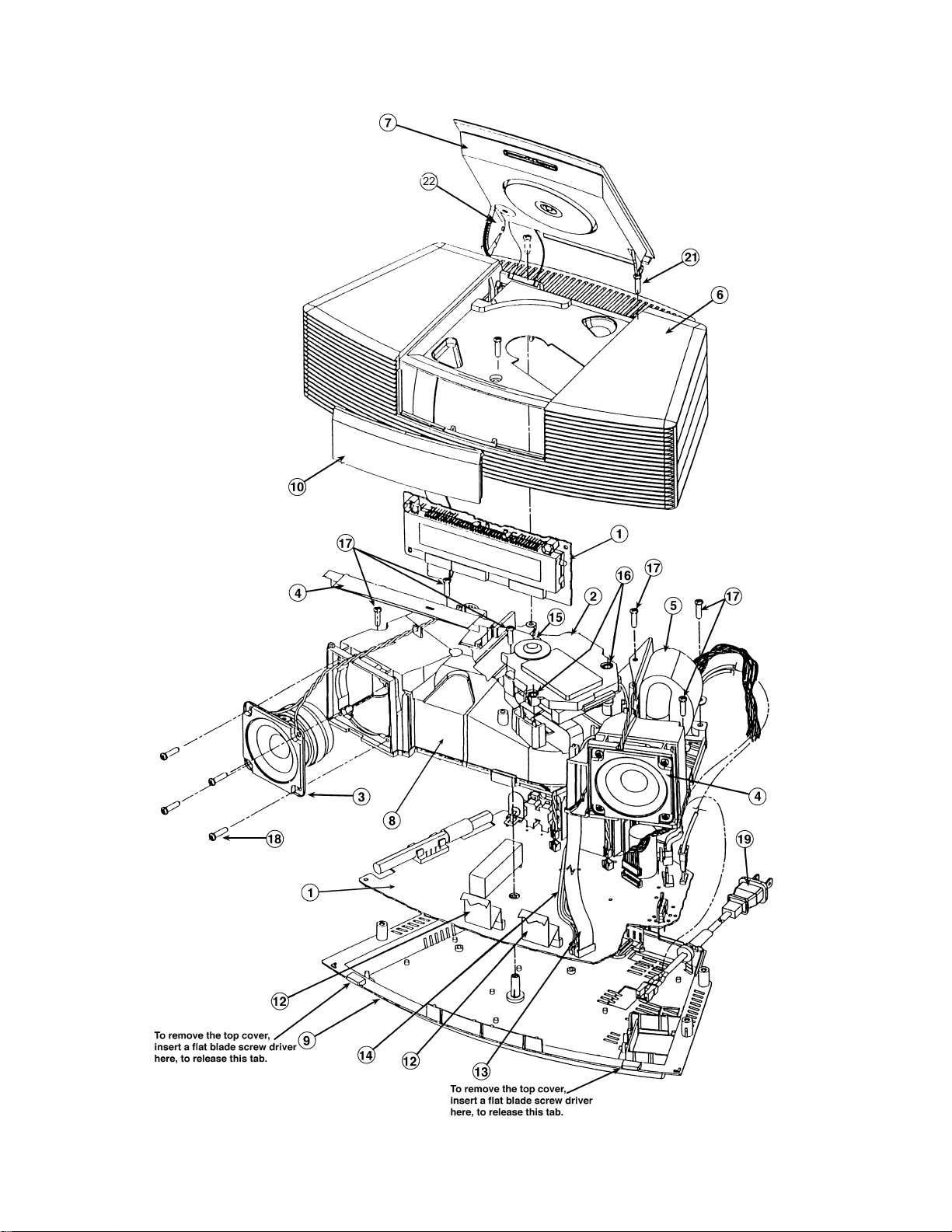
Figure 3. System Exploded View
20
Page 22
ELECTRICAL PART LIST
Resistors
Reference
Designator
R110MEG., CF, 1/2W, 5% 250891 3, 4
R1 10MEG, LINE, 1/2W, 5% 250891 3, 7
R2 POLYSWITCH, 60V 194090
R6 10 OHM, CHIP, 0805, 5% 133626-1005
R8 33.2K, CHIP, 0805, 1/10W, 1% 133625-3322
R9 47.0K, 0805, 1/10W, 5% 133626-4735
R10 47.0K, 0805, 1/10W, 5% 133626-4735
R200 47.0K, 0805, 1/10W, 5% 133626-4735
R201 4.7K, CHIP, 0805, 5% 133626-4725
R202 10.0K, 0805, 1/10W, 5% 133626-1035
R203 10.0K, 0805, 1/10W, 5% 133626-1035
R204 4.7K, CHIP, 0805, 5% 133626-4725
R205 47.0K, 0805, 1/10W, 5% 133626-4735
R206 47.0K, 0805, 1/10W, 5% 133626-4735
R207 15 OHM, FUSING, .25W 130102-150 3
R208 330 OHM, 2512, 1W, 5% 181895-3300
R210 10.0K, 0805, 1/10W, 5% 133626-1035
R211 15 OHM, FUSING, .25W 130102-150 3
Description Part Number Note
R212 510 OHM, 2010, 1/2W, 5% 187608-5115
R214 5.1 OHM, FUSING, .25W 130102-150 3
R215 10.0K, 0805, 1/10W, 5% 133626-1035
R220 1.00K, 0805, 1/10W, 5% 133626-1025
R222 100K, 0805, 1/10W, 5% 133626-1045
R223 100K, 0805, 1/10W, 5% 133626-1045
R230 100K, 0805, 1/10W, 5% 133626-1045
R231 10.0K, 0805, 1/10W, 1% 133625-1002
R232 3.32K, 0805, 1/10W, 1% 133625-3321
R300 1.00K, 0805, 1/10W, 5% 133626-1025
R301 120 OHM, 0805, 1/10W, 1% 133625-1200
R302 2.32K, 0805, 1/10W, 1% 133625-2321
R303 499 OHM, CHIP, 0805, 1/10W, 1% 133625-4990
R304 2.32K, 0805, 1/10W, 1% 133625-2321
R305 330 OHM, 0805, 1/10W, 1% 133625-3300
R306 51 OHM, 0805, 1/10W, 5% 133626-5105
R307 4.7K, CHIP, 0805, 5% 133626-4725
R308 4.99K, 0805, 1/10W, 1% 133625-4991
R309 4.02K, 0805, 1/10W, 1% 133625-4021
R310 47.0K, 0805, 1/10W, 5% 133626-4735
R311 30.1 OHM, 0805, 1/10W, 1% 133625-30R1
R313 20 OHM, 0805, 1/10W, 5% 133626-2005
21
Page 23
ELECTRICAL PART LIST
Resistors (continued)
Reference
Designator
R417 10.0K, 0805, 1/10W, 5% 133626-1035
R418 10.0K, 0805, 1/10W, 5% 133626-1035
R419 1.0K, ARRAY, SMT, 4 POS, 5% 186433-1024
R420 1.0M, 0805, 1/10W, 1% 133625-1004
R421 10.0K, 0805, 1/10W, 5% 133626-1035
R422 100K, 0805, 1/10W, 5% 133626-1045 5, 6
R422 10.0K, 0805, 1/10W, 5% 133626-1035 4
R428 82K, CHIP, 0805, 1/10W, 5% 133626-8235
R429 82K, CHIP, 0805, 1/10W, 5% 133626-8235
R430 681 OHM, CHIP, 0805, 1/10W, 1% 133625-6810
R431 82K, CHIP, 0805, 1/10W, 5% 133626-8235
R432 82K, CHIP, 0805, 1/10W, 5% 133626-8235
R440 220 OHM, 4 POS ARRAY, SMT, 5% 186433-2214
R441 2.7K, 4 POS, ARRAY, SMT, 5% 186433-2724
R442 2.7K, 4 POS, ARRAY, SMT, 5% 186433-2724
R443 2.7K, 4 POS, ARRAY, SMT, 5% 186433-2724
R445 10.0K, 0805, 1/10W, 5% 133626-1035
R447 5.10K, 0805, 1/10W, 5% 133626-5125
R448 10.0K, 0805, 1/10W, 5% 133626-1035
R449 3.01K, 0805, 1/10W, 1% 133625-3011
R450 1.0M, 0805, 1/10W, 1% 133625-1004
R455 10.0K, 0805, 1/10W, 5% 133626-1035
R460 1.0M, 0805, 1/10W, 1% 133625-1004
R461 51 OHM, 0805, 1/10W, 5% 133626-5105
R462 10.0K, 0805, 1/10W, 5% 133626-1035
R463 150 OHM, CHIP, 0805, 1/10W, 1% 133625-1500
R464 243 OHM, 0805, 1/10W, 1% 133625-2430
R465 47 OHM, CHIP, 0805, 1/10W, 5% 133626-4705
R466 10.0K, 0805, 1/10W, 5% 133626-1035
R467 47.0K, 0805, 1/10W, 5% 133626-4735
R468 681 OHM, CHIP, 0805, 1/10W, 1% 133625-6810
R469 681 OHM, CHIP, 0805, 1/10W, 1% 133625-6810
R470 681 OHM, CHIP, 0805, 1/10W, 1% 133625-6810
R471 6.80K, 0805, 1/10W, 5% 133626-6825
R472 6.80K, 0805, 1/10W, 5% 133626-6825
R473 6.80K, 0805, 1/10W, 5% 133626-6825
R474 6.80K, 0805, 1/10W, 5% 133626-6825
R475 16.5K, CHIP, 0805, 1% 133625-1652
R476 16.5K, CHIP, 0805, 1% 133625-1652
R477 1.00K, 0805, 1/10W, 5% 133626-1025
R480 2.7K, 4 POS, ARRAY, SMT, 5% 186433-2724
R485 10.0K, 0805, 1/10W, 5% 133626-1035
R490 510 OHM, 0805, 1/10W, 5% 133626-5115
R491 510 OHM, 0805, 1/10W, 5% 133626-5115
Description Part Number Note
22
Page 24
ELECTRICAL PART LIST
Resistors (continued)
Reference
Designator
R495 JUMPER, CHIP, 0805 133627
R500 1.00K, 0805, 1/10W, 5% 133626-1025
R501 499 OHM, CHIP, 0805, 1/10W, 1% 133625-4990
R503 13.3K, 0805, 1/10W, 1% 133625-1332
R504 27.4K, CHIP, 0805, 1/10W, 1% 133625-2742
R505 562 OHM, 0805, 1/10W, 1% 133625-5620
R506 1.00K, 0805, 1/10W, 5% 133626-1025
R507 100K, 0805, 1/10W, 1% 133625-1003
R508 68.1K, 0805, 1/10W, 1% 133625-6812
R509 15.0K, 0805, 1/10W, 1% 133625-1502
R510 3.32K, 0805, 1/10W, 1% 133625-3321
R513 1 OHM, 0805, 1/10W, 5% 133626-1R05
R514 8.25K, CHIP, 0805, 1/10W, 1% 133625-8251
R515 2.21K, CHIP, 0805, 1/10W, 1% 133625-2211
R516 221K, 0805, 1/10W, 1% 133625-2213
R519 15.0K, 0805, 1/10W, 1% 133625-1502
R520 22.1K, 0805, 1/10W, 1% 133625-2212
R521 7.50K, 0805, 1/10W, 1% 133625-7501
R522 7.50K, 0805, 1/10W, 1% 133625-7501
R527 1 OHM, 0805, 1/10W, 5% 133626-1R05
R528 12.7K, 0805, 1/10W, 1% 133625-1272
R529 33.2K, CHIP, 0805, 1/10W, 1% 133625-3322
R530 20.0K, CHIP, 0805, 1/10W, 1% 133625-2002
R531 2.21K, CHIP, 0805, 1/10W, 1% 133625-2211 10
R531 2.74K, 0805, 1/10W, 1% 133625-2741 9
R532 56.2K, CHIP, 0805, 1%, 133625-5622
R533 1.82K, 0805, 1/10W, 1% 133625-1821
R534 56.2K, CHIP, 0805, 1% 133625-5622
R535 221K, 0805, 1/10W, 1% 133625-2213
R536 221K, 0805, 1/10W, 1% 133625-2213
R537 15.0K, 0805, 1/10W, 1% 133625-1502
R538 22.1K, 0805, 1/10W, 1% 133625-2212
R539 270K, 0805, 1/10W, 5% 133626-2745
R540 332 OHM, CHIP, 0805, 1% 133625-3320
R543 10.0K, 0805, 1/10W, 1% 133625-1002
R544 47.5K, CHIP, 0805, 1/10W, 1% 133625-4752
R545 33.2K, CHIP, 0805, 1/10W, 1% 133625-3322
R546 22.1K, 0805, 1/10W, 1% 133625-2212
R547 12.1K, 0805, 1/10W, 1% 133625-1212
R548 1.00K, CHIP, 0805, 1/10W, 1% 133625-1001
R549 15.0K, 0805, 1/10W, 1% 133625-1502
R550 332 OHM, CHIP, 0805, 1% 133625-3320
R551 1.21K, 0805, 1/10W, 1% 133625-1211
R552 681 OHM, CHIP, 0805, 1/10W, 1% 133625-6810
Description Part Number Note
23
Page 25
ELECTRICAL PART LIST
Resistors (continued)
Reference
Designator
R553 68.1K, 0805, 1/10W, 1% 133625-6812
R554 1.00K, 0805, 1/10W, 5% 133626-1025
R555 7.50K, 0805, 1/10W, 1% 133625-7501 10
R555 15K, CHIP, 0805, 1/10W, 5% 133626-1535 9
R556 15.0K, 0805, 1/10W, 1% 133625-1502
R557 1 OHM, 0805, 1/10W, 5% 133626-1R05
R558 20 OHM, 0805, 1/10W, 5% 133626-2005
R559 47.0K, 0805, 1/10W, 5% 133626-4735
R560 15.0K, 0805, 1/10W, 1% 133625-1502
R561 1.00K, 0805, 1/10W, 5% 133626-1025
R562 27.4K, CHIP, 0805, 1/10W, 1% 133625-2742
R565 10 OHM, CHIP, 0805, 5% 133626-1005
R566 1.00K, 0805, 1/10W, 5% 133626-1025
R568 47.0K, 0805, 1/10W, 5% 133626-4735
R569 2.21K, CHIP, 0805, 1/10W, 1% 133625-2211
R570 2.21K, CHIP, 0805, 1/10W, 1% 133625-2211
R571 7.50K, 0805, 1/10W, 1% 133625-7501
R571 JUMPER, CHIP, 0805 133627
R572 221K, 0805, 1/10W, 1% 133625-2213
R573 221K, 0805, 1/10W, 1% 133625-2213
R574 1.00K, 0805, 1/10W, 5% 133626-1025
R575 1.00K, 0805, 1/10W, 5% 133626-1025
R580 10.0K, 0805, 1/10W, 5% 133626-1035
R600 10.0K, 0805, 1/10W, 1% 133625-1002
R601 10.0K, 0805, 1/10W, 1% 133625-1002
R603 1.10K, 0805, 1/10W, 1% 133625-1101
R604 14.7K, CHIP, 0805, 1% 133625-1472
R605 1.10K, 0805, 1/10W, 1% 133625-1101
R606 14.7K, CHIP, 0805, 1% 133625-1472
R607 5.62K, CHIP, 0805, 1/10W, 1% 133625-5621
R608 12.7K, 0805, 1/10W, 1% 133625-1272
R609 35.7K, 0805, 1/10W, 1% 133625-3572
R610 4.02K, 0805, 1/10W, 1% 133625-4021
R611 3.48K, 0805, 1/10W, 1% 133625-3481
R612 10.0K, 0805, 1/10W, 1% 133625-1002
R613 1.87K, 0805, 1/10W, 1% 133625-1871
R615 14.0K, CHIP, 0805, 1% 133625-1402
R616 6.81K, CHIP, 0805, 1/10W, 1% 133625-6811
R617 6.81K, CHIP, 0805, 1/10W, 1% 133625-6811
R618 1.40K, 0805, 1/10W, 1% 133625-1401
R619 10.5K, 0805, 1/10W, 1% 133625-1052
R620 11.3K, 0805, 1/10W, 1% 133625-1132
R621 3.74K, 0805, 1/10W, 1% 133625-3741
R622 30.1K, CHIP, 0805, 1/10W, 1% 133625-3012
Description Part Number Note
24
Page 26
ELECTRICAL PART LIST
Resistors (continued)
Reference
Designator
R623 4.75K, 0805, 1/10W, 1% 133625-4751
R624 1.27K, 0805, 1/10W, 1% 133625-1271
R625 14.0K, CHIP, 0805, 1% 133625-1402
R626 41.2K, 0805, 1/10W, 1% 133625-4122
R627 715 OHM, 0805, 1/10W, 1% 133625-7150
R628 2.10K, 0805, 1/10W, 1% 133625-2101
R629 3.74K, 0805, 1/10W, 1% 133625-3741
R630 8.87K, 0805, 1/10W, 1% 133625-8871
R631 8.87K, 0805, 1/10W, 1% 133625-8871
R632 1.10K, 0805, 1/10W, 1% 133625-1101
R633 26.7K, 0805, 1/10W, 1% 133625-2672
R634 787 OHM, 0805, 1/10W, 1% 133625-7870
R635 25.5K, 0805, 1/10W, 1% 133625-2552
R636 2.00K, 0805, 1/10W, 1% 133625-2001
R637 221K, 0805, 1/10W, 1% 133625-2213
R638 25.5K, 0805, 1/10W, 1% 133625-2552
R639 475 OHM, 0805, 1/10W, 1% 133625-4750
R640 10.2K, CHIP, 0805, 1/10W, 1% 133625-1022
R642 15.0K, 0805, 1/10W, 1% 133625-1502
R643 8.2K, CHIP, 0805, 1/10W, 5% 133626-8225
R645 4.22K, 0805, 1/10W, 1% 133625-4221
R647 1.00K, 0805, 1/10W, 5% 133626-1025
R649 100K, 0805, 1/10W, 5% 133626-1045
R650 1.00K, 0805, 1/10W, 5% 133626-1025
R651 100K, 0805, 1/10W, 5% 133626-1045
R655 75.0K, 0805, 1/10W, 1% 133625-7502
R656 4.99K, 0805, 1/10W, 1% 133625-4991
R657 75.0K, 0805, 1/10W, 1% 133625-7502
R659 1.00K, 0805, 1/10W, 5% 133626-1025
R660 4.99K, 0805, 1/10W, 1% 133625-4991
R662 1.00K, 0805, 1/10W, 5% 133626-1025
R663 150K, 0805, 1/10W, 1% 133625-1503
R664 1.00K, 0805, 1/10W, 5% 133626-1025
R665 1.00K, 0805, 1/10W, 5% 133626-1025
R666 1.00K, 0805, 1/10W, 5% 133626-1025
R667 1.00K, CHIP, 0805, 1/10W, 1% 133625-1001
R668 100K, 0805, 1/10W, 1% 133625-1003
R669 100K, 0805, 1/10W, 1% 133625-1003
R670 10.0K, 0805, 1/10W, 5% 133626-1035
R672 1.00K, CHIP, 0805, 1/10W, 1% 133625-1001
R674 1.78K, 0805, 1/10W, 1% 133625-1781
Description Part Number Note
25
Page 27
ELECTRICAL PART LIST
Capacitors
Reference
Designator
C1 33pF, CER, 85, 400VAC, 20% 183627-330 3, 4, 7
C2 .1uF, 1206, X7R, 25V, 5% 131754-104
C3 .1uF, 1206, X7R, 25V, 5% 131754-104
C4 .1uF, 1206, X7R, 25V, 5% 131754-104
C5 .1uF, 1206, X7R, 25V, 5% 131754-104
C6 10kuF, EL, 105, 25V, 20% 171555
C7 .22uF, BOX, 85, 50V, 5% 137127-224
C8 .47uF, BOX, 85, 50V, 5% 137127-474
C9 220pF, 0805, COG, 50V, 5% 133622-221
C10 220pF, 0805, COG, 50V, 5% 133622-221
C11 .01uF, 0805, X7R, 50V, 10% 133623-103
C12 100uF, EL, 85, 16V, 20% 149947-101C
C13 .001uF, 1206, COG, 50V, 5% 177214-102
C15 .10uF, 0805, Y5V, 25V, 80% 133624
C16 2200uF, EL, 105C, 16V, 20% 198458-222C
C20 .047uF, 0805, X7R, 50V, 10% 133623-473
C200 .047uF, 0805, X7R, 50V, 10% 133623-473
C201 .047uF, 0805, X7R, 50V, 10% 133623-473
C202 470uF, EL, 105, 35V, 20% 144000-471V
C203 .047uF, 0805, X7R, 50V, 10% 133623-473
C205 470UF, EL, 105, 35V, 20% 144000-471V
C209 .047uF, 0805, X7R, 50V, 10% 133623-473
C210 .047uF, 0805, X7R, 50V, 10% 133623-473
C211 330pF, 0805, COG, 50V, 5% 133622-331
C215 .047uF, 0805, X7R, 50V, 10% 133623-473
C216 .047uF, 0805, X7R, 50V, 10% 133623-473
C217 .10uF, 0805, Y5V, 25V, 80% 133624
C218 10uF, EL, 105, 16V, 20% 137126-100
C219 .10uF, 0805, Y5V, 25V, 80% 133624
C220 2.2uF, EL, 85, 50V, 20% 149947-2R2H
C221 100pF, 0805, COG, 50V, 5% 133622-101
C225 .047uF, 0805, X7R, 50V, 10% 133623-473
C226 330pF, 0805, COG, 50V, 5% 133622-331
C227 330pF, 0805, COG, 50V, 5% 133622-331
C229 2.2uF, EL, 85, 50V, 20% 149948-2R2H
C231 .047uF, 0805, X7R, 50V, 10% 133623-473
C232 .047uF, 0805, X7R, 50V, 10% 133623-473
C233 1uF, 1206, Y5V, 16V, 80% 173383-105
C300 1000pF, 0805, COG, 50V, 5% 133622-102
C301 .047uF, 0805, X7R, 50V, 10% 133623-473
C302 47uF, EL, 85, 16V, 20% 149947-470C
C303 .047uF, 0805, X7R, 50V, 10% 133623-473
Description Part Number Note
26
Page 28
ELECTRICAL PART LIST
Capacitors (continued)
Reference
Designator
C304 6.8pF, CHIP, 0805, 50V, 5% 133622-6R8
C305 .047uF, 0805, X7R, 50V, 10% 133623-473
C307 20pF, TRIM, NPO, 100V 197314-T200
C308 430pF, 0805, COG, 50V, 2% 177269-431
C309 47uF, EL, 85, 25V, 20% 149948-470E
C310 .047uF, 0805, Z5U, 20% 148779-473
C311 3.3uF, EL, 85, 50V, 20% 149948-3R3H
C312 .047uF, 0805, Z5U, 20% 148779-473
C313 47uF, EL, 85, 25V, 20% 149948-470E
C314 2.2UF, MONO, 1206, Y5V, 16V, 80% 178212-225
C315 .01uF, 0805, X7R, 50V, 10% 133623-103
C316 .047uF, 0805, Z5U, 20% 148779-473
C317 47uF, EL, 85, 25V, 20% 149948-470E
C318 2.2uF, EL, 85, 50V, 20% 149948-2R2H
C319 .047uF, 0805, Z5U, 20% 148779-473
C320 1.0uF, EL, 85, 50V, 20% 149948-1R0H
C321 .47uF, EL, 85, 50V, 20% 149948-R47H
C323 1.0uF, EL, 85, 50V, 20% 149948-1R0H
C325 10uF, EL, 85, 25V, 20% 149948-100E
C328 1.0uF, EL, BP, 85, 50V, 20% 147522-1R0
C329 10uF, EL, 85, 25V, 20% 149948-100E
C330 .047uF, 0805, X7R, 50V, 10% 133623-473 4
C330 .033uF, 0805, X7R, 50V, 10% 133623-333 5, 6, 7
C331 .047uF, 0805, X7R, 50V, 10% 133623-473 4
C331 .033uF, 0805, X7R, 50V, 10% 133623-333 5, 6, 7
C332 1000pF, 0805, COG, 50V, 5% 133622-102
C333 1.0uF, EL, 85, 50V, 20% 149948-1R0H
C335 2.2uF, EL, BP, 85, 50V, 20% 147522-2R2
C336 .01uF, 0805, X7R, 50V, 10% 133623-103
C337 1000pF, 0805, COG, 50V, 5% 133622-102
C338 1000pF, 0805, COG, 50V, 5% 133622-102
C339 1000pF, 0805, COG, 50V, 5% 133622-102
C340 3300pF, 0805, X7R, 50V, 10% 133623-332
C341 27pF, 0805, COG, 50V, 5% 133622-270 10
C341 39pF, 0805, COG, 50V, 5% 133622-390 9
C342 27pF, 0805, COG, 50V, 5% 133622-270 10
C342 39pF, 0805, COG, 50V, 5% 133622-390 9
C343 .047uF, 0805, X7R, 50V, 10% 133623-473
C344 100UF, EL, BP, 85, 16V, 20% 147522-101
C345 .047uF, 0805, X7R, 50V, 10% 133623-473
C348 1000pF, 0805, COG, 50V, 5% 133622-102
C349 1000pF, 0805, COG, 50V, 5% 133622-102
C355 1000pF, 0805, COG, 50V, 5% 133622-102
C356 100pF, 0805, COG, 50V, 5% 133622-101
Description Part Number Note
27
Page 29
ELECTRICAL PART LIST
Capacitors (continued)
Reference
Designator
C357 100pF, 0805, COG, 50V, 5% 133622-101
C358 10uF, EL, 85, 25V, 20% 149947-100E
C359 4.7uF, EL, 85, 50V, 20% 149947-4R7H
C360 330pF, 0805, COG, 50V, 5% 133622-331
C365 1.0uF, EL, 85, 50V, 20% 149948-1R0H
C366 1.0uF, EL, 85, 50V, 20% 149948-1R0H
C367 1800pF, 0805, COG, 50V, 5% 133622-182
C368 1800pF, 0805, COG, 50V, 5% 133622-182
C371 330pF, 0805, COG, 50V, 5% 133622-331
C375 330pF, 0805, COG, 50V, 5% 133622-331
C376 330pF, 0805, COG, 50V, 5% 133622-331
C377 1000pF, 0805, COG, 50V, 5% 133622-102
C378 .10uF, 0805, Y5V, 25V, 80% 133624
C380 330pF, 0805, COG, 50V, 5% 133622-331
C381 330pF, 0805, COG, 50V, 5% 133622-331
C382 1000pF, 0805, COG, 50V, 5% 133622-102
C384 100pF, 0805, COG, 50V, 5% 133622-101
C385 100pF, 0805, COG, 50V, 5% 133622-101
C386 100pF, 0805, COG, 50V, 5% 133622-101
C387 1000pF, 0805, COG, 50V, 5% 133622-102
C388 33pF, 0805, COG, 50V, 5% 133622-330
C400 330pF, 0805, COG, 50V, 5% 133622-331
C401 330pF, 0805, COG, 50V, 5% 133622-331
C402 330pF, 0805, COG, 50V, 5% 133622-331
C403 330pF, 0805, COG, 50V, 5% 133622-331
C404 330pF, 0805, COG, 50V, 5% 133622-331
C405 330pF, 0805, COG, 50V, 5% 133622-331
C406 3300pF, 0805, X7R, 50V, 10% 133623-332
C407 3300pF, 0805, X7R, 50V, 10% 133623-332
C408 3300pF, 0805, X7R, 50V, 10% 133623-332
C409 3300pF, 0805, X7R, 50V, 10% 133623-332
C410 3300pF, 0805, X7R, 50V, 10% 133623-332
C411 3300pF, 0805, X7R, 50V, 10% 133623-332
C412 .047uF, 0805, Z5U, 20% 148779-473
C413 330pF, 0805, COG, 50V, 5% 133622-331
C414 330pF, 0805, COG, 50V, 5% 133622-331
C415 1000pF, 0805, COG, 50V, 5% 133622-102
C416 330pF, 0805, COG, 50V, 5% 133622-331
C417 .01uF, 0805, X7R, 50V, 10% 133623-103
C418 100pF, 0805, COG, 50V, 5% 133622-101
C419 1000pF, 0805, COG, 50V, 5% 133622-102
C422 100pF, 0805, COG, 50V, 5% 133622-101
C423 100pF, 0805, COG, 50V, 5% 133622-101
C424 100pF, 0805, COG, 50V, 5% 133622-101
Description Part Number Note
28
Page 30
ELECTRICAL PART LIST
Capacitors (continued)
Reference
Designator
C425 1000pF, 0805, COG, 50V, 5% 133622-102
C426 2.2uF, MONO, 1206, Y5V, 16V, 80% 178212-225
C434 47pF, 0805, COG, 50V, 5% 133622-470
C435 47pF, 0805, COG, 50V, 5% 133622-470
C436 47pF, 0805, COG, 50V, 5% 133622-470
C437 47pF, 0805, COG, 50V, 5% 133622-470
C438 1.0uF, 1206, Y5V, 25V, 80% 198609-105
C439 1.0uF, 1206, Y5V, 25V, 80% 198609-105
C440 15uF, TANT, 25V, 10%, D SIZE 196981-
C441 180pF, 0805, COG, 50V, 5% 133622-181
C442 820pF, 0805, COG, 50V, 5% 133622-821
C443 820pF, 0805, COG, 50V, 5% 133622-821
C444 820pF, 0805, COG, 50V, 5% 133622-821
C445 2200pF, 0805, X7R, 50V, 10% 133623-222
C446 820pF, 0805, COG, 50V, 5% 133622-821
C447 820pF, 0805, COG, 50V, 5% 133622-821
C448 820pF, 0805, COG, 50V, 5% 133622-821
C449 820pF, 0805, COG, 50V, 5% 133622-821
C450 820pF, 0805, COG, 50V, 5% 133622-821
C451 820pF, 0805, COG, 50V, 5% 133622-821
C452 180pF, 0805, COG, 50V, 5% 133622-181
C453 820pF, 0805, COG, 50V, 5% 133622-821
C454 820pF, 0805, COG, 50V, 5% 133622-821
C455 820pF, 0805, COG, 50V, 5% 133622-821
C456 4700pF, 0805, X7R, 50V, 10% 133623-472
C457 820pF, 0805, COG, 50V, 5% 133622-821
C458 820pF, 0805, COG, 50V, 5% 133622-821
C459 820pF, 0805, COG, 50V, 5% 133622-821
C460 820pF, 0805, COG, 50V, 5% 133622-821
C461 .1uF, 1206, X7R, 25V, 5% 131754-104
C462 330pF, 0805, COG, 50V, 5% 133622-331
C463 330pF, 0805, COG, 50V, 5% 133622-331
C464 330pF, 0805, COG, 50V, 5% 133622-331
C465 .01uF, 0805, X7R, 50V, 10% 133623-103
C466 .10uF, 0805, Y5V, 25V, 80% 133624
C467 15uF, TANT, 25V, 10%, D SIZE 196981-
C468 1uF, 1206, Y5V, 16V, 80% 173383-105
C469 330pF, 0805, COG, 50V, 5% 133622-331
C470 100pF, 0805, COG, 50V, 5% 133622-101
C471 100pF, 0805, COG, 50V, 5% 133622-101
C472 1000pF, 0805, COG, 50V, 5% 133622-102
C473 1000pF, 0805, COG, 50V, 5% 133622-102
Description Part Number Note
E156D1
E156D1
29
Page 31
ELECTRICAL PART LIST
Capacitors (continued)
Reference
Designator
C474 1000pF, 0805, COG, 50V, 5% 133622-102
C475 .01uF, 0805, X7R, 50V, 10% 133623-103
C476 1000pF, 0805, COG, 50V, 5% 133622-102
C477 1000pF, 0805, COG, 50V, 5% 133622-102
C478 330pF, 0805, COG, 50V, 5% 133622-331
C479 330pF, 0805, COG, 50V, 5% 133622-331
C480 330pF, 0805, COG, 50V, 5% 133622-331
C481 330pF, 0805, COG, 50V, 5% 133622-331
C482 330pF, 0805, COG, 50V, 5% 133622-331
C483 330pF, 0805, COG, 50V, 5% 133622-331
C485 330pF, 0805, COG, 50V, 5% 133622-331
C490 4700pF, 0805, X7R, 50V, 10% 133623-472
C491 4700pF, 0805, X7R, 50V, 10% 133623-472
C492 4700pF, 0805, X7R, 50V, 10% 133623-472
C493 1000pF, 0805, COG, 50V, 5% 133622-102
C494 1000pF, 0805, COG, 50V, 5% 133622-102
C495 1000pF, 0805, COG, 50V, 5% 133622-102
C502 10uF, EL, 85, 25V, 20% 149947-100E
C503 .22uF, BOX, 85, 50V, 5% 137127-224
C504 330pF, 0805, COG, 50V, 5% 133622-331
C505 .015uF, BOX, 85, 100V, 5% 137127-153
C506 .033uF, BOX, 85, 63V, 5% 137127-333
C507 .033uF, BOX, 85, 63V, 5% 137127-333
C508 .0068uF, BOX, 85, 100V, 5% 137127-682
C509 .15uF, BOX, 85, 50V, 5% 137127-154
C510 220uF, EL, 85, 6.3V, 20% 149947-221J
C511 .01uF, 0805, X7R, 50V, 10% 133623-103
C512 .15uF, BOX, 85, 50V, 5% 137127-154
C513 .033uF, BOX, 85, 63V, 5% 137127-333
C514 .01uF, BOX, 85, 100V, 5% 137127-103
C519 .022uF, 0805, X7R, 50V, 10% 133623-223
C520 100uF, EL, 85, 16V, 20% 149947-101C
C521 100uF, EL, 85, 16V, 20% 149947-101C
C522 .01uF, 0805, X7R, 50V, 10% 133623-103
C523 10uF, EL, 85, 25V, 20% 149947-100E
C524 1.0uF, EL, 85, 50V, 20% 149947-1R0H
C525 .15uF, BOX, 85, 50V, 5% 137127-154
C526 .15uF, BOX, 85, 50V, 5% 137127-154
C527 .01uF, BOX, 85, 100V, 5% 137127-103
C528 220pF, 0805, COG, 50V, 5% 133622-221
C529 .0033uF, BOX, 85, 100V, 5% 137127-332
C530 .01uF, BOX, 85, 100V, 5% 137127-103
C531 10uF, EL, 85, 25V, 20% 149947-100E
C532 47uF, EL, 85, 16V, 20% 149947-470C
Description Part Number Note
30
Page 32
ELECTRICAL PART LIST
Capacitors (continued)
Reference
Designator
C533 .47uF, EL, BP, 85, 50V, 20% 147522-R47
C534 4.7uF, EL, 85, 50V, 20% 149947-4R7H
C535 .33uF, BOX, 85, 50V, 5% 137127-334
C536 .1uF, BOX, 85, 50V, 5% 137127-104
C537 .01uF, BOX, 85, 100V, 5% 137127-103
C538 .001uF, BOX, 85, 100V, 5% 137127-102
C539 3.9pF, 0805, COG, 50V, 5% 133622-3R9
C540 100pF, 0805, COG, 50V, 5% 133622-101
C541 12pF, 0805, COG, 50V, 5% 133622-120
C542 .01uF, BOX, 85, 100V, 5% 137127-103
C543 .1uF, BOX, 85, 50V, 5% 137127-104
C544 .1uF, BOX, 85, 50V, 5% 137127-104
C545 .10uF, 0805, Y5V, 25V, 80% 133624
C546 100pF, 0805, COG, 50V, 5% 133622-101
C547 10pF, 0805, COG, 50V, 5% 133622-100
C548 10pF, 0805, COG, 50V, 5% 133622-100
C549 .10uF, 0805, Y5V, 25V, 80% 133624
C550 100uF, EL, 85, 16V, 20% 149947-101C
C551 .10uF, 0805, Y5V, 25V, 80% 133624
C552 47uF, EL, 85, 16V, 20% 149947-470C
C553 .10uF, 0805, Y5V, 25V, 80% 133624
C554 .01uF, 0805, X7R, 50V, 10% 133623-103
C555 4.7uF, EL, 85, 50V, 20% 149947-4R7H
C556 4.7uF, EL, 85, 50V, 20% 149947-4R7H
C557 .10uF, 0805, Y5V, 25V, 80% 133624
C558 1.0uF, EL, 85, 50V, 20% 149947-1R0H
C559 .047uF, 0805, X7R, 50V, 10% 133623-473
C560 1000pF, 0805, COG, 50V, 5% 133622-102
C561 .047uF, 0805, Z5U, 20% 148779-473
C562 1000pF, 0805, COG, 50V, 5% 133622-102
C563 220pF, 0805, COG, 50V, 5% 133622-221
C570 330pF, 0805, COG, 50V, 5% 133622-331
C571 330pF, 0805, COG, 50V, 5% 133622-331
C572 1000pF, 0805, COG, 50V, 5% 133622-102
C600 .1uF, BOX, 85, 50V, 5% 137127-104
C601 .027uF, BOX, 85, 63V, 5% 137127-273
C602 .01uF, BOX, 85, 100V, 5% 137127-103
C603 .01uF, BOX, 85, 100V, 5% 137127-103
C605 .18uF, BOX, 85, 50V, 5% 137127-184
C606 .18uF, BOX, 85, 50V, 5% 137127-184
C607 .33uF, BOX, 85, 50V, 5% 137127-334
C608 .33uF, BOX, 85, 50V, 5% 137127-334
C609 .0047uF, BOX, 85, 100V, 5% 137127-472
C610 820pF, 0805, COG, 50V, 5% 133622-821
Description Part Number Note
31
Page 33
ELECTRICAL PART LIST
Capacitors (continued)
Reference
Designator
C611 .033uF, BOX, 85, 63V, 5% 137127-333
C612 .033uF, BOX, 85, 63V, 5% 137127-333
C613 .0056uF, BOX, 85, 100V, 5% 137127-562
C614 .01uF, BOX, 85, 100V, 5% 137127-103
C615 .01uF, BOX, 85, 100V, 5% 137127-103
C616 .1uF, BOX, 85, 50V, 5% 137127-104
C617 .1uF, BOX, 85, 50V, 5% 137127-104
C618 .0022uF, BOX, 85, 100V, 5% 137127-222
C619 820pF, 0805, COG, 50V, 5% 133622-821
C620 .47uF, BOX, 85, 50V, 5% 137127-474
C621 .47uF, BOX, 85, 50V, 5% 137127-474
C622 .047uF, BOX, 85, 63V, 5% 137127-473
C623 .047uF, BOX, 85, 63V, 5% 137127-473
C624 10uF, EL, 85, 25V, 20% 149947-100E
C627 .1uF, 1206, X7R, 25V, 5% 131754-104
C628 .1uF, 1206, X7R, 25V, 5% 131754-104
C629 .1uF, 1206, X7R, 25V, 5% 131754-104
C630 2.2uF, EL, 85, 50V, 20% 149947-2R2H
C631 2.2uF, EL, 85, 50V, 20% 149947-2R2H
C634 100pF, 0805, COG, 50V, 5% 133622-101
C635 100pF, 0805, COG, 50V, 5% 133622-101
C636 2.2uF, EL, 85, 50V, 20% 149947-2R2H
C637 2.2uF, EL, 85, 50V, 20% 149947-2R2H
C639 1000pF, 0805, COG, 50V, 5% 133622-102
C640 100pF, 0805, COG, 50V, 5% 133622-101
C641 100pF, 0805, COG, 50V, 5% 133622-101
C642 22uF, EL, 85, 16V, 20% 149947-220C
C645 .18uF, BOX, 85, 50V, 5% 137127-184
C646 .18uF, BOX, 85, 50V, 5% 137127-184
C647 4.7uF, EL, 85, 50V, 20% 149947-4R7H
C650 2.2UF, EL, 85, 50V, 20% 149947-2R2H
C651 1000pF, 0805, COG, 50V, 5% 133622-102
C652 1000pF, 0805, COG, 50V, 5% 133622-102
C655 100pF, 0805, COG, 50V, 5% 133622-101
C656 100pF, 0805, COG, 50V, 5% 133622-101
C657 100pF, 0805, COG, 50V, 5% 133622-101
C658 100pF, 0805, COG, 50V, 5% 133622-101
C665 .18uF, BOX, 85, 50V, 5% 137127-184
C666 .18uF, BOX, 85, 50V, 5% 137127-184
C667 2.2uF, EL, BP, 85, 50V, 20% 147522-2R2
C681 2.2uF, EL, BP, 85, 50V, 20% 147522-2R2
C682 100pF, 0805, COG, 50V, 5% 133622-101
C683 100pF, 0805, COG, 50V, 5% 133622-101
C684 100pF, 0805, COG, 50V, 5% 133622-101
Description Part Number Note
32
Page 34
ELECTRICAL PART LIST
Capacitors (continued)
Reference
Designator
C685 100pF, 0805, COG, 50V, 5% 133622-101
C686 470uF, EL, 85, 16V, 20% 149948-471C
C687 .01uF, 0805, X7R, 50V, 10% 133623-103
C688 .01uF, 0805, X7R, 50V, 10% 133623-103
C689 .1uF, 0805, X7R, 50V, 10% 133623-103
Reference
Designator
D1 BAV99, DUAL, SOT-23 147239
D3 DUAL, SOT-23, COMMON NEG 250682
D200 SMT, S1G 178380-4
D201 SMT, S1G 178380-4
D202 DUAL, SOT-23, COMMON NEG 250682
D203 DIODE, SHOTTKY, BAT42W, SOD-123 196984-002
D204 BAV99, DUAL, SOT-23 147239
D206 BAV99, DUAL, SOT-23 147239
D207 DUAL, SOT-23, COMMON NEG 250682
D211 DUAL, SOT-23, COMMON NEG 250682
D212 BAV99, DUAL, SOT-23 147239
D213 BAV99, DUAL, SOT-23 147239
D300 BAV99, DUAL, SOT-23 147239
D302 BAV99, DUAL, SOT-23 147239
D304 DIODE, VARACTOR, DUAL, 20V, 50mA 177495-5
D305 BAV99, DUAL, SOT-23 147239
D401SENSOR, LIGHT, VISIBLE187629-001
D600 DUAL, SOT-23, COMMON NEG 250682
ZR200 1N5232, ZENER, 5.6V, 225MW 135247-5232
BR1 KBJ601G, RECTIFIER, BRIDGE 187611-001 3
Description Part Number Note
Diodes
Description Part Number Note
Transistors
Reference
Designator
Q4 SOT23, BPLR, P, 40V, 200mA 148596
Q200 SOT23, BPLR, N, 50V, 100mA 146817
Q201 TO-92, BPLR, P, 60V, 200mA 119168
Q202 TO-92, BPLR, P, 60V, 200mA 119168
Q206 TO-92, BPLR, P, 60V, 200mA 119168
Q207 SOT23, BPLR, N, 4.7K 192603
Q208 TO-92, BPLR, P, 60V, 200mA 119168
Description Part Number Note
33
Page 35
ELECTRICAL PART LIST
Transistors (continued)
Reference
Designator
Q209 SOT23, BPLR, N, 50V, 100mA 146817
Q210 SOT23, BPLR, P, 40V, 200mA 148596
Q211 BPLR, P, SOT, HI-HFE 252042
Q212 MOSFET, N, SOT 252043
Q300 2SA1341, P, 50V 146818
Q301 SOT23, BPLR, N, 50V, 100mA 146817
Q303 SOT-23, BPLR, N, 25V, 30mA 187601-001
Q304 SOT23, BPLR, N, 55V, 150mA 134741
Q400 2SA1341, P, 50V 146818
Q401 SENSOR, IR DETECTING 182493-38
Q402 2SA1341, P, 50V 146818
Q403 2SA1341, P, 50V 146818
Q404 2SA1341, P, 50V 146818
Q405 SOT-23, NPN, HIHfe 250681
Q406 SOT-23, NPN, HIHfe 250681
Q500 SOT23, BPLR, P, 40V, 200mA 148596
Q501 2SD8790V, TO-92, N 193457
Q600 2SA1341, P, 50V 146818
Q602 2SA1341, P, 50V 146818
Q603 SOT23, BPLR, N, 50V, 100mA 146817
Description Part Number Note
Integrated Circuits
Reference
Designator
U1 TDA7375A, POWER AMP, MW15 250117
U200 VOLT REG, 15V, NEG, TO-92 193423-15
U201 LM78M10, T220 178352-10
U202 VOLT REG, POS, 5V, LO-VD/IQ 193401-05R0
U203 LM78M05, T220 178352-05
U300 AM/FM TUNER, SO-20LA1836 187600-001
U301 PLL FREQ SYNTH, MFP-24 199693 10
U301 LC72131, PLL FREQ SYNTH, MFP-20 187733-001 9
U400UC, MASKED, REV3.8 253545-03R6
U401 EEPROM, 1K, 24C01A 184044
U403 RESET, SOT23, MAX809, 4.63V 191158-01
U500 LA9241M, CD ASP, QFP64 187721-001
U501 LC78622E, CD DSP, QFP64 187722-001
U502 LA6541D, MTR DRIVER, DIP30 193432
U600 TLO74D, QUAD OPAMP, SOIC 186112
U601 TLO74D, QUAD OPAMP, SOIC 186112
U603 NJM13700, TRANS, DUAL, SOIC-16 188650-001
U605 TDA7313, VOL CONT, DIP 28/SO28 177983
Description Part Number Note
34
Page 36
ELECTRICAL PART LIST
Filters
Reference
Designator
CF300 FILTER, CER, 10.7MHz, 230kHz 253037-002
CF301FILTER, CER, 10.7MHZ, 180kHZ, FGD253037-001
CF302 RESONATOR, CERAMIC, 456kHz 187604-001
CF303 CRYSTAL, FUND, 7.2MHz, HC-49/S 250892-001
CF401 RESONATOR, CER, 8 MHZ 191446-8R00
CF500 CRYSTAL, 16.9344MHZ, HC-49/S 193415-001
T300 DETECTOR, FM, SINGLE TUNED 187602-001
T301 FILTER, CER, AM IF 187603-001
T302 COIL, OSCILLATOR, AM 180647
T303 FILTER, STEREO MPX, SINGLE TUNED 187624-001
T304 FILTER, STEREO MPX, SINGLE TUNED 187624-001
Reference
Designator
L1 2.2uH, COMMON MODE 187598-2R2 3
L2 2.2uH, COMMON MODE 187598-2R2 3
Description Part Number Note
Inductors
Description Part Number Note
L3 BEAD, 17.5MM 170179
L4 BEAD, 17.5MM 170179
L300 400 OHMS, CHIP, 0805 188587-401
L400 400 OHMS, CHIP, 0805 188587-401
L401 400 OHMS, CHIP, 0805 188587-401
L402 400 OHMS, CHIP, 0805 188587-401
L403 400 OHMS, CHIP, 0805 188587-401
L404 400 OHMS, CHIP, 0805 188587-401
Miscellaneous
Reference
Designator
FM-TUNER TUNER, FM, 87.5TO 108 MHZ, SHIELD
TUNER, FM,4 GANG, 7V
TUNER, FM, 76-90MHZ, 7V
F1FUSE,1.0 A, 250V135677-05
VFD DISPLAY, VFD, 4-GRID 251147
J1 HEADER, LOCKING, TOP-ENTRY 193369-002 3
Description Part Number Note
251054
184589
188466-001
135677-03
4
5, 6
7
3, 4, 7
3, 6, 7
35
Page 37
ELECTRICAL PART LIST
Miscellaneous (continued)
Reference
Designator
J2 CONN, HEADER, 5.0MM, 5A, 2 PIN 191946-002 3
J3 CONN, HEADER, 8 POS 148591-08 3
J5 HEADER, PCB MNT, 2 POS 193422-002
J6 HEADER, PCB MNT, 2 POS 193422-002
J200 CABLE, BATTERY/ADAPTER, 9 VOLT 187610-001
J300 FM ANTENNA, F-TYPE 193453 4, 7
J300 FM ANTENNA, PAL TYPE 193455 5, 6
J301 RECEPTACLE, TOP-ENTRY 191423-21
J400 CONN, HEADER, 3 POS 148591-03
J401 HEADER, RTANG, 21 PIN, FCC 191169-21
J402 HEADER, RTANG, 21 PIN, FCC 191169-21
J403 HEADER, RTANG, 15 PIN, WHITE 191169-15
J500 HEADER, 13P, TOP-ENTRY, ZIF 193368-013
J501 RECEPTACLE, TOP-ENTRY 191423-21
J502 HEADER, LOW CURRENT 6 POLE 133224-06
J600 CONN, HOUSING, PHONO, QUAD 149959
FOR-D401 SPACER, LED 193426
FOR-Q401 SPACER, LED 193426
FOR-U300 SHIELD, IC 178944
AM-ANT ANTENNA, FERRITE BAR 177268
SCREW, TAPP, M3.5x0.6x10, PAN, TRX 140447-10
CLIP, SPRING 142864
HEATSINK 177562
SHIELD, BOTTOM, DISPLAY PCB 198610
HOLDER, VFD 199955
Description Part Number Note
36
Page 38
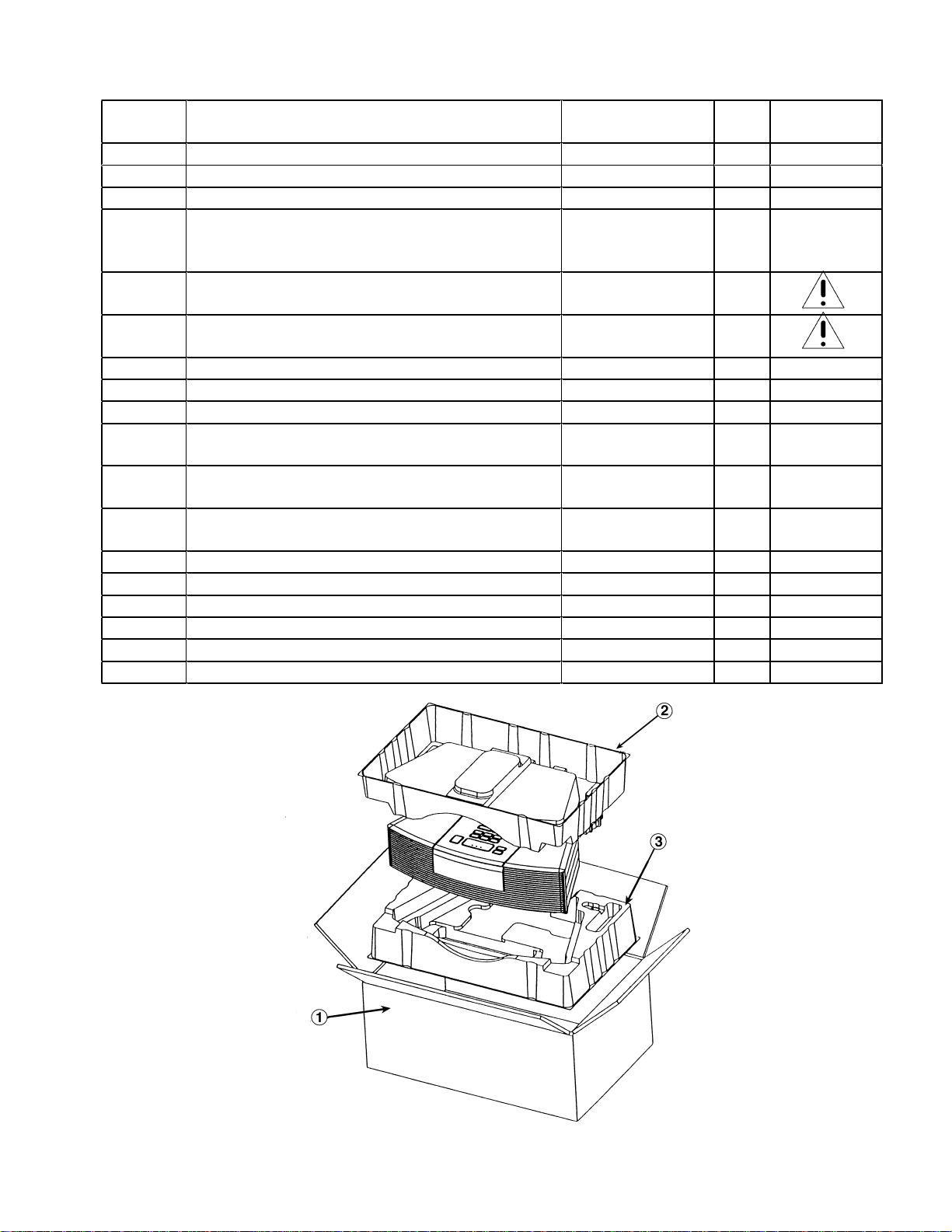
PACKAGING PART LIST
r
Item
Numbe
1 CARTON, RSC 199479-001 1
2 PACKING, THERMO TRAY, TOP 250843 1
3 PACKING, THERMO TRAY, BOTTOM 250844 1
- REMOTE, IMPERIAL WHITE
REMOTE, PLATINUM WHITE
REMOTE, GRAPHITE GREY
- BATTERY, LITHIUM 180991 1 3
- BATTERY, 9V, CARBON 187609-001 1 3
- VELCRO, HOOK AND LOOP, MATED 188463-001 1
- CD, DEMO, US 193340 1
- LETTER, COMMITMENT 251001 1
- MANUAL, OWNER’S, ENGLISH
MANUAL, OWNER’S, 4 LANG.
- ANTENNA, FM, DIPOLE, PAL CONN
ANTENNA, FM DIPOLE, 75 OHM, F CONN
- SHEET, QUICK START, 120V
QUICK START, 230V/240V
- CABLE, AUDIO, 2 POS, BLK 183879-02 1
- BAG, POLY, 14.38 x 9.87 x 2mil 103351 1
- BROCHURE, ALL PRODUCT 188898 1
- WARRANTY CARD 251497 1
- DECLARATION OF CONFORMITY 251918 1
- SHEET, BUFFER 251743 1
Description Part Number Qty. Note
193334-001
193334-010
193334-002
250723
251771
143185
148589
250722
251772
1
14
5, 6
1 5, 6
4, 7, 8
1
Figure 4. Packaging View
37
Page 39

ABBREVIATED OPERATING INSTRUCTIONS
Note: Refer to the Bose® Wave® Radio/CD owner’s guide 250723 for complete operating instruc-
tions.
To turn off the display- With the system off, hold down CD Mode and press On/Off to turn off the
main display. The display only lights briefly when you press any button and while the alarm is sounding.
Repeat this step to turn the main display back on.
To set AM/PM (12 hour) or Military (24 hour) time- With the system off, hold down Alarm Setup
and press On/Off to switch between AM/PM (12 hour) and Military (24 hour) time formats.
To adjust the display brightness- The display dims automatically to medium or low brightness, as
appropriate for low light room conditions. You can adjust the brightness setting of the display for both
strong light and lowest light environments, but not for the medium light setting. Turn the system off
before setting the brightness levels.
In a strong lit room, hold down CD Mode and press Volume up or down to adjust the setting
between 6 and 9 (it is preset to 8).
In a barely lit room, hold down CD Mode and press Volume up or down to adjust the setting
between 1 and 6 (it is preset to 2).
If you do not want the system to dim automatically, set both levels to 5.
To manually tune in a station- Tap either Track/Tune button quickly two or more times to tune the
frequency in small step. Or, press and hold either Track/Tune button until the desired station is
reached. Then, you can press the button to adjust the frequency in small steps. After manually
tuning, wait two seconds for the system to return to seek mode.
To set the alarm volume- While the selected alarm is flashing, press Volume up or down to set
the alarm volume, from 10 to 99. The selected alarm flashes for ten seconds.
To set continuous music- In CD play mode, to select a source to play automatically after the CD
ends, hold down Alarm Setup and press FM, AM, or AUX on the control panel only. The selected
source lights briefly on the display. Cancel continuous play by pressing CD stop or On/Off.
Page 40
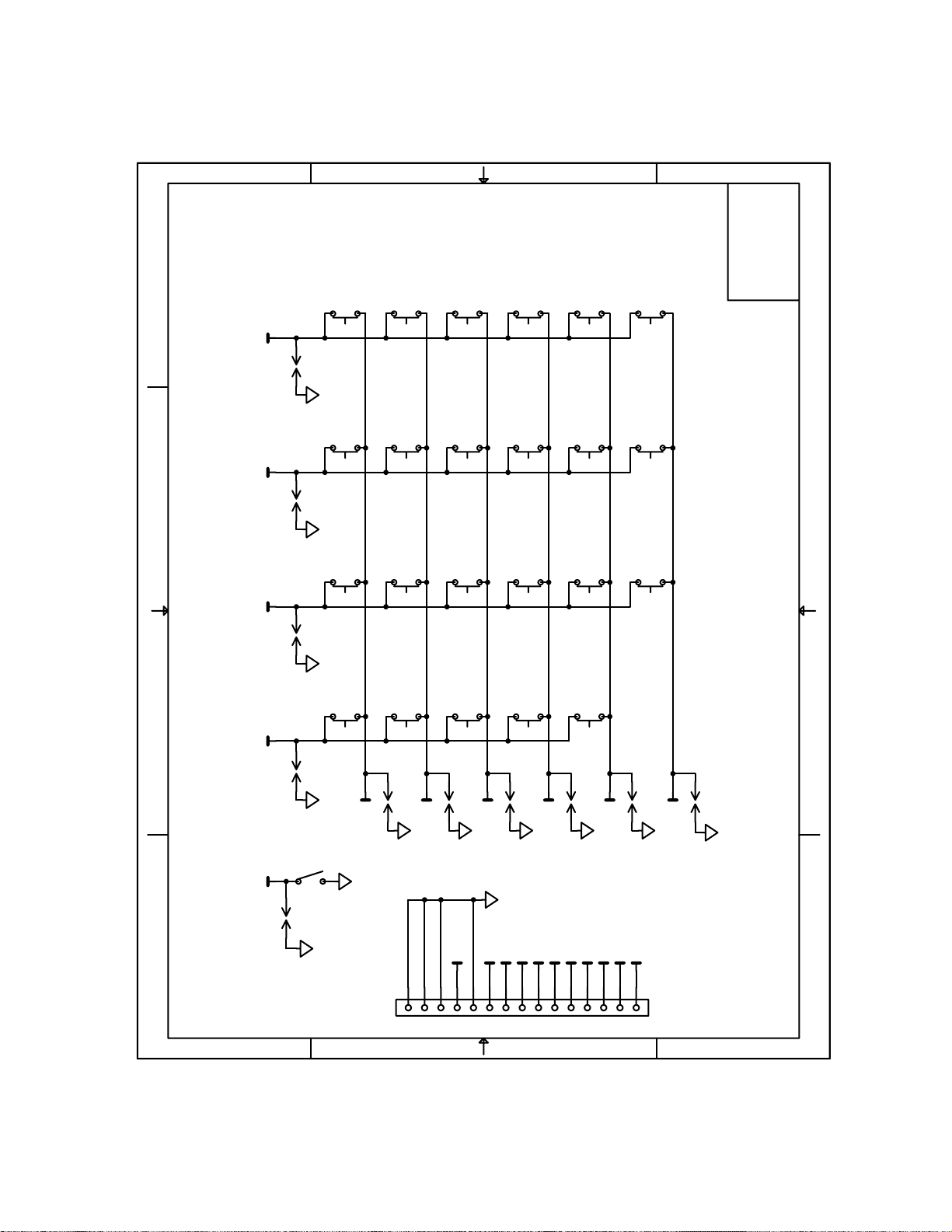
D
C
B
A
1234
PCB 193386
KEYPAD
SD 193386
CD_PLAY_PAUSERANDOM_REPEAT
KEYIN1
DDDD
BWR/CD 250443
KEYIN2
KEYIN3
KEYIN4
DOOR-SW
TIME_FORWARD VOLUME_DOWN SLEEP_SNOOZE ON_OFF
KEYOUT3
D
TIME_BACK PRESET_6 PRESET_5 PRESET_4
D
KEYOUT2
ALARMS_SETUP PRESET_3 PRESET_2 PRESET_1
D
KEYOUT4
D
CD_STOP
D
KEYOUT1
ALARM2_ON_OFF
KEYOUT6
ALARM1_ON_OFF VOLUME_UP TRACK_TUNE_UP TRACK_TUNE_DOWN
D
AM
AUX FM
D
D
KEYOUT5
D
DOOR_SWITCH
KEYIN1
13
KEYOUT4
15
14
DOOR-SW
KEYIN2
KEYIN3
5
KEYIN4
KEYOUT6
7
6
KEYOUT1
9
8
KEYOUT2
11
10
KEYOUT3
12
KEYOUT5
4
3
2
1
4321
J1
D
C
B
A
Figure 5. Keyboard Schematic Diagram
Page 41

Specifications and Features Subject to Change Without Notice
Bose Corporation
The Mountain
Framingham Massachusetts USA 01701
P/N 250443 REV. 04 10/99 For Technical Assistance or Part Orders, Call 1-800-367-4008
 Loading...