

Page 1

CONTENTS
Safety Information............................................................................................................................ 3
Electrostatic Discharge Sensitive (ESDS) Device Handling ........................................................ 4
Warranty Information....................................................................................................................... 4
Theory of Operation, Opti-Voice
Theory of Operation, Opti-Source™ Option Card...................................................................... 7-8
Theory of Operation, FreeSpace
General Information ....................................................................................................................... 10
Disassembly/Assembly Procedures ....................................................................................... 11-12
Figure 1. AmPlus™ 100 Rear Panel .............................................................................................. 11
Figure 2. Option Card Installation .................................................................................................. 11
Figure 3. Top Cover Removal ........................................................................................................ 11
Figure 4. EQ Card Installation........................................................................................................ 11
Figure 5. Top Cover Replacement ................................................................................................. 12
Opti-Voice Page Option Card Controls ................................................................................... 13-15
Opti-Source Option Card Controls ..........................................................................................16-18
AmPlus 100 Test Setup Parameters ............................................................................................. 19
Table 1. AmPlus 100 Initial Switch Settings ................................................................................... 19
Table 2. AmPlus 100 Signal Inputs Table ....................................................................................... 19
Table 3. AmPlus 100 Signal Outputs Table .................................................................................... 19
Test Procedures ........................................................................................................................ 20-31
Table 4. Opti-Source Option Card Initial Switch Positions ............................................................. 20
Table 5. Opti-Source Option Card Signal Inputs ............................................................................ 20
Table 6. Opti-Voice Page Option Card Initial Switch Positions....................................................... 24
Table 7. Opti-Voice Page Option Card Signal Inputs ..................................................................... 24
Table 8. Opti-Voice Page Option Card Signal Outputs................................................................... 24
Table 9. AmPlus 100 Amplifier Initial Switch Settings..................................................................... 28
Table 10. AmPlus 50 Amplifier Initial Switch Settings..................................................................... 28
Table 12. FreeSpace Model 1B Flush EQ Frequency Response Tests ......................................... 29
Table 11. FreeSpace Model 1B Surface EQ Frequency Response Tests...................................... 29
Table 13. Model 8 Full Range Response Tests.............................................................................. 30
Table 14. Model 8 High Frequency Response Tests...................................................................... 31
Table 15. Model 25/32 Full Range Response Tests....................................................................... 31
Table 16. Model 25/32 High Frequency Response Tests............................................................... 31
Part List Notes................................................................................................................................ 32
Product Code Listing..................................................................................................................... 32
Electrical Part List, Opti-Voice Page Card .............................................................................. 33-35
Packing List, Opti-Voice Page Card (see Figure 6) ..................................................................... 36
Figure 6. Opti-Voice Page Card Packing View............................................................................... 36
Electrical Part List, Opti-Source Option Card ........................................................................ 37-39
Packing List, Opti-Source Option Card (see Figure 7) ............................................................... 39
Figure 7. Opti-Source Option Card Packing View.......................................................................... 39
FreeSpace Model 1B EQ Card Part List .................................................................................. 40-41
Packing List, FreeSpace Model 1B EQ card (see Figure 8) ...................................................... 41
Figure 8. FreeSpace Model 1B EQ Card Packing View................................................................. 41
Model 8 EQ Card Part List ........................................................................................................ 42-43
Packing List, Model 8 EQ Card (see Figure 9)............................................................................. 43
Figure 9. Model 8 Equalizer PCB Packing View ............................................................................ 43
Model 25/32 EQ Card Part List ................................................................................................. 44-45
Packing List, Model 25/32 EQ Card (see Figure 10).................................................................... 45
Figure 10. Model 25/32 Equalizer PCB Packing View ................................................................... 45
®
Page Option Card ................................................................. 5-6
®
Model 1B Equalizer Card........................................................ 9
1
Page 2

CONTENTS
Note: This document has been updated with information from supplement 194101-S3.
This affects part numbers for the switches used on the Opti-Voice Page card and the
Opti-Source Option card. Refer to supplement 194101-S3 for more information.
Main Part List, FreeSpace
®
Zone 2 Remote Control with A/B Switch (see Figure 11) ............. 46
Figure 11. FreeSpace Zone 2 Remote Control with A/B Switch Exploded View............................ 46
Main Part list, FreeSpace Zone 2 Remote Volume Control w/o A/B Switch (see Figure 12) ... 47
Figure 12. FreeSpace Zone 2 Remote Volume Control w/o A/B Switch Exploded View ............... 47
Integrated Circuit Pinout Diagrams......................................................................................... 48-49
General Troubleshooting Tips ................................................................................................. 50-51
®
Troubleshooting the Opti-Voice
Page Card................................................................................ 52
Troubleshooting the Opti-Source™ Option Card........................................................................ 53
Figure 13. FreeSpace Model 1B Equalizer Board Topside and Etch Layout Diagram................... 54
Figure 14. FreeSpace Model 1B Equalizer Board SMD and Etch Layout Diagram ....................... 54
Figure 15. Models 8 and 25/32 Equalizer PCB Topside Component and Etch Layout Diagram ... 55
Figure 16. Models 8 and 25/32 SMD Component and Etch Layout Diagram ................................ 55
Figure 17. Models 8 and 25/32 Equalizer PCB Schematic Diagram.............................................. 56
CAUTION: The AmPlus™ 100 and AmPlus 50 Amplifier
Option and Equalizer Cards contain no user serviceable
parts. To prevent warranty infractions, refer servicing to
warranty service centers or factory service.
PROPRIETARY INFORMATION
THIS DOCUMENT CONTAINS PROPRIETARY INFORMATION OF
BOSE
®
CORPORATION WHICH IS BEING FURNISHED ONLY
FOR THE PURPOSE OF SERVICING THE IDENTIFIED BOSE
PRODUCT BY AN AUTHORIZED BOSE SERVICE CENTER OR
OWNER OF THE BOSE PRODUCT, AND SHALL NOT BE
REPRODUCED OR USED FOR ANY OTHER PURPOSE.
2
Page 3

SAFETY INFORMATION
1. Parts that have special safety characteristics are identified by the symbol on
schematics or by special notes on the parts list. Use only replacement parts that
have critical characteristics recommended by the manufacturer.
2. Make leakage current or resistance measurements to determine that exposed
parts are acceptably insulated from the supply circuit before returning the unit
to the customer. Use the following checks to perform these measurements:
A. Leakage Current Hot Check
(1) With the unit completely reassembled, plug the AC line cord directly
into a 120V AC outlet. Do not use an isolation transformer during
this test. Use a leakage current tester or a metering system that
complies with American National Standards Institute (ANSI) C101.1
"Leakage Current for Appliances" and Underwriters Laboratories
(UL) 1492 (71).
(2) With the unit AC switch first in the ON position and then in the OFF position,
measure from a known earth ground (metal water pipe, conduit, etc.) to all
exposed metal parts of the unit (antennas, handle bracket, metal cabinet,
screwheads, metallic overlays, control shafts, etc.), especially any
exposed metal parts that offer an electrical return path to the chassis.
(3) Any current measured must not exceed 0.5 milliamp.
(4) Reverse the unit power cord plug in the outlet and repeat test.
ANY MEASUREMENTS NOT WITHIN THE LIMITS SPECIFIED HEREIN
INDICATE A POTENTIAL SHOCK HAZARD THAT MUST BE ELIMINATED
BEFORE RETURNING THE UNIT TO THE CUSTOMER.
B. Insulation Resistance Test Cold Check
(1) Unplug the power supply and connect a jumper wire between the two
prongs of the plug.
(2) Turn on the power switch of the unit.
(3) Measure the resistance with an ohmmeter between the jumpered AC plug
and each exposed metallic cabinet part on the unit. When the exposed
metallic part has a return path to the chassis, the reading should be
between 1 and 5.2 Megohms. When there is no return path to the chassis,
the reading must be "infinite". If it is not within the limits specified, there is the
possibility of a shock hazard, and the unit must be repaired and rechecked
before it is returned to the customer.
3
Page 4

ELECTROSTATIC DISCHARGE SENSITIVE
(ESDS) DEVICE HANDLING
This unit contains ESDS devices. We recommend the following precautions when repairing,
replacing, or transporting ESDS devices:
• Perform work at an electrically grounded work station.
• Wear wrist straps that connect to the station or heel straps that connect to conductive floor
mats.
• Avoid touching the leads or contacts of ESDS devices or PC boards even if properly
grounded. Handle boards by the edges only.
• Transport or store ESDS devices in ESD protective bags, bins, or totes. Do not insert
unprotected devices into materials such as plastic, polystyrene foam, clear plastic bags,
bubble wrap, or plastic trays.
WARRANTY INFORMATION
The following products are covered by a 5-year transferable limited warranty.
• Opti-Voice
• Opti-Source™ Option Card
• FreeSpace
• Model 8 Equalizer PCB
• Model 25/32 Equalizer PCB
®
Page Option Card
®
Model 1B Equalizer Card
4
Page 5

THEORY OF OPERATION
Opti-Voice® Page Option Card
Introduction
This card accepts a pair of mic or line level sources at its Page 1 and Page 2 inputs at
J1. These signals are amplified in three variable gain stages, passed through a muting
circuit, and presented to a line out source selector. The page signals are also mixed with
the signals fed to the Page option card from the AmPlus™ 100 and fed back into the
AmPlus 100.
Sheet 1 of 2
Refer to the Opti-Voice Page Option Card schematic diagram, sheet 1 of 2 for the
following information.
Note: The designators inside the brackets “[ ]” are the schematic grid coordinates which
are provided in order to make it easier to locate components on the schematic sheet
indicated in the description.
The Page 1 and Page 2 inputs at J1 [B/C8] accept any source from mic to line level
sources. U100A [D7], and U100B [A7] are differential input amplifiers, with inputs well
protected against RF and ESD, and with gain selectable between 0 and +30dB by
switches S1 [C7], and S2 [A7]. The amplified page signals pass through U101B [D7],
and U102B [A6], stages with gain controllable between 0 and +20dB by R1 [D6], and R2
[A6]. After this stage, S3 [D5], and S4 [B5] select whether the page signals pass through
another adjustable gain stage (U101A, U102A) or through a limiter. The adjustable gain
stage can range between -20 and +10dB, controlled by R1, 2. If the page signal is routed
through the limiter, the limiter can automatically control the gain, from -20 to +10dB, in
response to the signal level coming in. The compressor is implemented with U106 [C6],
U103C [C6], and U104C [B6]. U106 has a current in/current out gain cell providing
negative feedback around the op amps. The gain cell is controlled by an internal level
detector circuit which monitors the signal applied to the limiter. Once the input signal has
risen beyond the threshold, the detector reduces the stage gain with a slope of nearly
1dB/1dB, holding the output level nearly constant over a 30dB variation in input level.
Op amps U103A, B [C5] and U104A, B [B5] watch the highest of the signal levels out
of the first two gains stages and the compressor itself. They also watch the voltage on
the compressor release capacitors. Ultimately, they drive a bi-color LED, D104[C4], and
D105 [B5]. When the compressor is active, the LED glows green and brightens as the
signal level and compressor action rise. If the level out of the compressor or one of the
gain stages approaches its linear limits, the LED changes to red to warn the installer that
the source gain has been set too high.
After the limiter, S3, 4 feed the signal into a page mute circuit. Connected to the junction
of two input resistors of the inverting gain stages U105A [D5], is a transistor pair, Q100,
101 [C5]. The same circuit is used for the other channel with U105B [A4] with transistors
Q102, 103 [A4]. When these transistors are turned on, they attenuate the page signal,
essentially turning it off. The transistors are controlled by the voltages PG MUTE1, 2,
which are developed by the page trigger circuits. The page trigger circuits begin with a
trigger level control, R3 [B3], and R4 [B2] which feeds the page signal through an amplifier
and half wave rectifier and comparator (U202C, D, [B2/3] and U202A, B [B2]). Signals
greater than about 0.8 volts trigger the comparator, turning on the Page Trigger Indicator
LED D104 [B1] and D105 [B1], setting VPG1, 2 [B1] high, and raising PG MUTE1 [A1],
and PG MUTE2 [B1]. Raising PG MUTE1, 2 disables the page mute transistor, allowing
the page signal to pass.
5
Page 6

THEORY OF OPERATION
Opti-Voice® Page Option Card
Sheet 1 of 2 (continued)
After the page mute circuits, the page signals take two paths. One path is into U200
[D3], U201 [C3], selector switches which can be DIP switch programmed to select among
music, page 1, page 2, and page 1 + page 2 signals (see chart on schematic). The
selected signals are passed through a buffer amplifier, U203A [C2], and U203B [D2] to
the Page Card line outputs at J3 [C1] (protected against EMC and ESD by the
associated resistors and capacitors). The second path takes the outputs from Page 1 [D1]
and Page 2 [A3] to Sheet 2.
Sheet 2 of 2
Refer to the Opti-Voice Page Option Card schematic diagram, Sheet 2 of 2 for the
following information.
Note: The designators inside the brackets “[ ]” are the schematic grid coordinates which
are provided in order to make it easier to locate components on the schematic sheet
indicated in the description.
The two page signals entering Sheet 2 are passed through Page 1, 2 [C8] Level Trim
Potentiometers R5, 6 [C8] and through U300 [C6], a 4 PST analog switch. Logic
comprised of U301 [B6] responds to the VPG1, 2 signals [B8] (which indicate that a page
signal is active) and looks at the Page Enable Zone Assignment switches (S6) [A7] to
decide whether or not U300 will pass the page signal(s) to the output. The selected and
active page signals are summed with the music signals in U304A [C4], and U304D [C3].
The music signals are those signals passed into this option card from the AmPlus™
amplifier. Before being summed, these music signals pass through ducker stages, U304B
[B/C5], U304C [C4], and U303A [B5], with U303B [C4]. U303A, B is a current controlled
transconductance amplifier that provides additional negative feedback around U304B, C
when the signals from Q300, 301 [B5] are active. This attenuates the music signal by
about 20dB while the page signal is active.
6
Page 7

THEORY OF OPERATION
Opti-Source™ Option Card
Introduction
Refer to the Opti-Source Source Option Card schematic diagram, sheet 1 of 2 for the
following information.
Note: The designators inside the brackets “[ ]” are the schematic grid coordinates which
are provided in order to make it easier to locate components on the schematic sheet
indicated in the description.
This card accepts a pair of line level sources at its CH1 and CH2 "B" inputs. It allows
automatic or manual selection of the A (supplied by the AmPlus™ 100) or B sources,
passes them optionally through a dynamic range compressor, and returns the signal to the
AmPlus signal path.
Sheet 1 of 2
The CH1 and CH2 "B" Inputs at J1 [C8] accept line level sources. U1A, B [B/C8] are
unity gain, differential input amplifiers, with inputs well protected against RF and ESD.
With S3 [B6] in the 2 CH position, each op amp sends its output through a TRIM
potentiometer (R1 [C7], and R2 [B6]) into a fade in circuit. When S3 is in the MONO
position, the CH1 B input is steered forward to both CH1 and CH2 paths, in mono.
U1C, D and U102A, B [B/C6] constitute a two channel fade in circuit. When S1, 2
[B/C2] are in the AUTO selection mode, circuits on Sheet 2 detect when the sources
connected to the A inputs at J1 on the rear of the AmPlus 100 amplifier become active.
When A is active, it will override the selection of the B input, turning B off and A on. When
A becomes inactive, the fade in circuit slowly fades the B signal back up to full volume
and switches from A to B. When S1, 2 are in the manual selection mode, switches external
to the AmPlus 100 force selection of the A or B sources, independently for CH1 and CH2,
if desired. The fade in circuit incorporates a transconductance amplifier in the feedback
path of a non-inverting op amp stage. As long as the currents IABC1 [D1] and IABC2
[A1] into U102 [C6] and [B6] are essentially off, there is only the negative feedback
provided by R115 [C6] and R121 [B6], and the stage gains are normal. When IABC
ramps up, U102 turns on and provides additional negative feedback, reducing the stage
gain by 20 or 30dB, fading the B input.
U200 [C3] and U201 [B3] are selector switches for the CH1 and CH2 A, B signals. The
CH1 selector, U200, can select among sources A left (CH1), B left (CH1), A mono
(CH1+CH2), and B mono (CH1+CH2). U201 behaves similarly for CH2. J3, A/B
REMOTE Connector [C1], accommodates two SPST normally open selector switches
(located on the Zone 2 Remote Volume Controls) that can be placed near the system
operator to allow manual selection between A and B sources.
7
Page 8

THEORY OF OPERATION
Opti-Source™ Option Card
Sheet 2 of 2
Refer to the Opti-Source Source Option Card schematic diagram, sheet 2 of 2 for the
following information.
Note: The designators inside the brackets “[ ]” are the schematic grid coordinates which
are provided in order to make it easier to locate components on the schematic sheet
indicated in the description.
U300 detects signal presence on the CH1 A source, if S1 [sheet 1 at C2] is in the
AUTO selection mode. U300A [D8] amplifies the source, while U300B, C [D7] comprise a
peak detector whose output goes low when the absolute value of U300A's output
exceeds about 1 volt. U300D [D7] provides adjustable time delay and hysteresis for the
detector output, which goes high when source activity is detected. This signal, SW1 [D1],
passed through D312, moves the signal selector U200 [sheet 1 at C3] to the A source
position. U302C, D [D5] provide the final processing needed to make the ramped current
drive needed for the fade in circuit on Sheet 1. U302D and Q300 [D5] perform voltage to
current conversion. U301 [A8], U302A, B, [A5/6] and Q301 [A5] provide the same function
for CH2.
Signals DRC1 [C8] and DRC2 [B8], coming from the source selectors U200 and U201
[B/C3] on Sheet 1, are presented to S4 [C4] and S5 [B5], respectively, so that they can
pass through or bypass the dynamic range compressor (U400 [B/C3], U401B [C4],
U402C [B3]). IF S4, 5 are set to ENABLE, the selected source is passed through the
Dynamic Range Compressor. The DRC provides up to 25dB of gain to low level signals,
gradually dropping back to 0dB gain for high level signals. This improves the audibility of
low level passages of CD quality, wide dynamic range source material. U400 contains
both the level detectors and current in/current out gain cells needed to turn op amps
U401B, 402C into a compressor. The compressor output passes through S4 and a buffer
stage before being returned to the AmPlus™ 100. Op amps U401C, A [C1/2] watch both
the signal level out of the compressor and the voltage on the compressor release
capacitors and drive a bi-color LED, D402 [C1]. When the compressor is active, the LED
glows green and brightens as the signal level and compressor action rise. If the level out
of the compressor approached its linear limits, the LED changes to red to warn the installer
that the source gain has been set too high.
Identical circuits handle CH2.
8
Page 9

THEORY OF OPERATION
FreeSpace® Model 1B Equalizer Card
Introduction
This card is intended for use in the AmPlus™ 50 and 100 amplifiers. It accepts a full range
(50Hz to 16kHz) signal, equalizes it, and passes a full range signal back to the main
amplifier signal path.
Refer to the Free Space Model 1B EQ Card schematic diagram, sheet 1 of 1 for the
following information.
Note: The designators inside the brackets “[ ]” are the schematic grid coordinates which
are provided in order to make it easier to locate components on the schematic sheet
indicated in the description.
The equalization is segmented, with one block (U2 and U1, all sections [D1-8])
dedicated to bass region equalization for the Model 1B Bass Module. Following the output
of this section, U2A [D1], the signal is presented to two parallel equalization paths, one
comprised of U3 [B4-7],U4B [C3], and dedicated to EQ for surface mounted Bose
Space System satellite speakers (Models 25, and 32). The other path, comprised of U5
[B4-7], U4A [B3] provides equalization for Bose Model 8 flush-mount satellite speakers.
®
Free
The operation of all three equalizers is similar. Considering the bass equalizer, we see
U2B's [D7] output passed through R8 [D7] and into the non-inverting input of U2A [D2].
This input is extended as a bus to which EQ sections Bass 1 [D6] and Bass 2 [D5] are
connected. These will introduce dips into the audio response. Section Bass 3 [D4] is
connected to a potentiometer straddling U2A non-inverting and inverting inputs. When the
wiper is moved toward the non-inverting input, the section introduces a dip; when moved
toward the inverting input, a peak.
Each of the EQ sections utilizes a gyrator-connected op amp in conjunction with a series
capacitor to simulate an LCR series tuned circuit. The values of the capacitors and
resistors are chosen to implement EQ dips and/or peaks at the appropriate frequency,
amplitude, and Q to realize the desired EQ curves. Each EQ section has optional steering
resistors that could allow other curves to be implemented in the future with the same card.
There are also some spare sections not currently used.
S1 [B2] selects either the flush or the surface mount EQ curve, while potentiometer R33
[D1] provides a boost/cut range of adjustment of the 90Hz bass region. Pin 12 of J1 [B2]
is grounded and is sensed by the dynamic EQ circuit on Sheet 2 of AmPlus 50 and 100.
9
Page 10

GENERAL INFORMATION
Opti-Voice
®
Page and Opti-Source™ Option Cards
The Opti-Voice Page and Opti-Source Option Cards are used with the AmPlus™ 100 Amplifier
only. They cannot be used in the AmPlus 50 Amplifier.
Note: If you have either a Source or Page Option Card, you may install it in either option card
slot. If you have one of each, you must install the Source Card in the first, or left-most from the
rear, slot. This is due to the music "ducking" feature of the Page Card, whereby the music
signal is muted during a page and then ramped back up to its previous level after the page is
completed. You can install two of either card into the same amplifier for extended source or
paging capabilities. You can also use several AmPlus 100 amplifiers in an extended system to
create a wide range of possible configurations. The Opti-Voice Page and Opti-Source Option
Card controls are explained on pages 13-18 to assist you in troubleshooting.
Equalizer Cards
The AmPlus Business Music Amplifiers can be used with various Equalizer PCBs plugged into
the internal slots to allow equalization for various Bose
®
loudspeakers. These include the
Model 1B Equalizer PCB, and the Model 8 and Model 25/32 Equalizer PCBs which are
documented in this manual.
10
Page 11

DISASSEMBLY/ASSEMBLY PROCEDURES
D
REFE
PERA
/OR P
CE TH
POSE
R INS
CEDU
FORM
Installation Instructions
1. Opti-Voice
®
Page and Opti-Source™
Option Cards
Note: Refer to Figures 1 and 2 for the
following procedures.
CAUTION
RISK OF ELECTRICAL SHOCK
DO NOT OPEN
AVIS
RISQUE DE CHOC ELECTRIQUE
NE PAS OUVRIR
O
AND
Figure 1. AmPlus™ 100 Rear Panel
1.1 Facing the rear of the AmPlus 100
Amplifier, remove the two screws that
secure the cover plate for the option card
slot that you wish to use.
Note: If you have both an Opti-Voice
and an Opti-Source Option Card, you must
install the Source card into the left slot,
because of the music "ducking" feature of
the Page card.
Page
2. FreeSpace® Model 1B, Model 8, and
Model 25/32 Equalizer Cards
Note: Refer to Figures 3, 4 and 5 for the
following procedures.
CAUTION
RISK OF ELECTRICAL SHOCK
DO NOT OPEN
AVIS
RISQUE DE CHOC ELECTRIQUE
NE PAS OUVRIR
TO REDUCE THE RISK OF FIRE OR ELECTRICAL SHOCK,
DO NOT EXPOSE THIS EQUIPMENT TO RAIN OR MOISTURE.
WARNING
REFER TO YOUR INSTRUCTION MANUAL FOR PROPER INSTALLATION AND
OPERATING PROCEDURES. INCORRECT WIRING MAY RESULT IN DAMAGE
AND/OR POOR PERFORMANCE.
Figure 3. Top Cover Removal
2.1 Using a phillips-head screwdriver,
remove the five screws that secure the
AmPlus amplifier top cover to the amplifier
chassis.
2.2 Lift the AmPlus amplifier top cover
straight off.
EQ CARD 1
EQ CARD 2
CAUTION
RISK OF ELECTRICAL SHOCK
DO NOT OPEN
AVIS
PAGE 1 PAGE 2
PAGE 1
GAIN LEVEL
-20 +30
TRIGGER LEVEL
OFF MIN MAX
Opti-voice
GAIN LEVEL
-20 +30
®
PAGE CARD
RISQUE DE CHOC ELECTRIQUE
NE PAS OUVRIR
PAGE 2
LINE OUTPUTSINPUTS
CH 1 CH 2
OFF MAX
MIN
TRIGGER LEVEL
TO REDU
DO NOT EX
REFER TO YOU
OPERATING PRO
AND/OR POOR PER
Figure 2. Option Card Installation
1.2 Slide the Option Card into the card
cage until it engages with the connector.
1.3 Secure the Option Card to the amplifier
with the two screws removed in step 1.1.
11
EQ CARD 1
J9
EQ CARD 2
J10
Figure 4. EQ Card Installation
2.3 On the Main PCB, you will see two
jacks marked J9 and J10. (On the AmPlus
50 amplifer you will see only J9).
2.4 Plug the EQ Card into either J9 or
J10, as appropriate for your installation,
until it is fully engaged into the connector.
Page 12

DISASSEMBLY/ASSEMBLY PROCEDURES
Note: The Equalizer PCB will only plug
into the connector one way.
2.5 Observing orientation, place the
amplifier top cover onto the Amplifier.
2.6 Secure the top cover to the amplifier
using the five screws removed in step 2.1.
(see Figure 5.)
CAUTION
RISK OF ELECTRICAL SHOCK
DO NOT OPEN
AVIS
RISQUE DE CHOC ELECTRIQUE
TO REDUCE THE RISK OF FIRE OR ELECTRICAL SHOCK,
NE PAS OUVRIR
DO NOT EXPOSE THIS EQUIPMENT TO RAIN OR MOISTURE.
WARNING
REFER TO YOUR INSTRUCTION MANUAL FOR PROPER INSTALLATION AND
OPERATING PROCEDURES. INCORRECT WIRING MAY RESULT IN DAMAGE
AND/OR POOR PERFORMANCE.
Figure 5. Top Cover Replacement
12
Page 13

OPTI-VOICE® PAGE OPTION CARD CONTROLS
Setting Internal switches
There are several switches on the Opti-Voice Page Option Card that must be set before the
card is installed into the AmPlus™ 100 amplifier.
1. Page Assignment switches - Use these microphone switches to send your page sources
to the required zones.
2. Microphone Pad switches - When using microphones, place the gain switch in the +30dB
position. For line level sources, place the switch in the 0dB position.
3. Opti-Voice Compressor switches - To engage the Opti-Voice compressor feature for
Channel 1 and/or Channel 2, place these switches in the "IN" position. Engage the compressor
when users vary how loudly they talk into the microphone or how closely they hold the
microphone to their mouths. The compressor maintains a constant output level for inputs
varying over a 30dB range. The gain LED will glow green when the compressor is active, but
flashes red if the paging circuit is close to being overloaded.
Note: Do not use the compressor when:
• There is a tendency for feedback (a howling or screeching noise caused by the
loudspeakers being picked up by the microphone).
• The source is a line level signal sent from a mixer or amplifier with similar signal processing.
4. Line Output Mix switches - Use these switches to set up a line output mix. If the line
output will not be used, leave the switches in their factory preset positions. Send music, page1,
page 2, or page 1/page 2 to the outputs using the table shown in the figure above.
Note: For a mix of page 1/page 2 and music, use the line outputs on the rear of the AmPlus
100 amplifier.
13
Page 14

OPTI-VOICE® PAGE OPTION CARD CONTROLS
Making connections and setting levels
Setting system controls
1. Set your system controls as follows (see figure above)
1. Page Source Gain control: Set to -20dB
2. Page Trigger level: Center
3. Page Level control: Center
4. AmPlus™ 100 remote control: Set to 3 o'clock (about 5dB of attenuation)
2. Connecting your page sources
1. Use the quick-connect terminal blocks to connect your page sources to the Opti-Voice Page
Option card page inputs, and to connect the line outputs to other peices of equipment in your
system.
3. Setting levels
1. During these system adjustments, have another person continuously speak into the
microphone while you adjust the controls. A music source should also be playing.
For best results, make sure the person who is speaking:
• Holds the microphone approximately 6 inches (15cm) away from his or her mouth.
• Speaks at a normal volume.
• Holds the microphone's push-to-talk switch ON during the adjustments.
Some microphones do not have a push-to-talk switch.
14
Page 15

OPTI-VOICE® PAGE OPTION CARD CONTROLS
2. To adjust the levels for the paging system, follow these steps:
1. While another person is speaking into the microphone, adjust the page trim on the
Opti-Voice card until the compressor LED on the Opti-Voice card flashes red during the
loudest speech passages. Then, turn the trim down slightly until the LED glows green at
all times. If the Opti-Voice compressors are disabled, turn the trim down slightly until the
LED no longer flashes red.
2. While continuing to speak into the microphone, slowly turn the page trigger level control
down (to the left) until paging is disabled and the page trigger LED no longer glows
green. Turn the page trigger level control back to the right until the paging comes ON
again.
3. Now have the speaker stop speaking. The page trigger LED should go out and the
music should fade back in.
4. Have the person resume speaking. The page returns and the music source has
disabled.
5. Adjust the page level until the person speaking is just loud enough to be heard clearly.
Note: Be sure to set the paging level loud enough to be heard in noisy environments,
such as when a room is filled with loud patrons.
6. If you are also using the Opti-Source™ card, ensure that the page/music balance is
good for both "A" and "B" sources. If the balance is poor, refer to the procedure in the
Opti-Source card section of this manual for setting source levels. After the "A" and "B"
source levels are satisfactorily set, return to this section to check the page/music
balance.
15
Page 16

OPTI-SOURCE™ OPTION CARD CONTROLS
CH. 1
S6
4
123
FADE DELAY
S7
4
3
12
CH. 2
SOURCE B
INPUT
MANUAL
CH. 1
AUTO
A/B MODE
MANUAL
CH. 2
AUTO
INPUT
MODE
CH. 1
GAIN
ENABLE
S1
CH. 1
DISABLE
COMPRESSORS
ENABLE
S2
LED'S
CH. 2
DISABLE
CH.1
LEVEL
CH. 2
GAIN
S4
S5
CH.2
LEVEL
LINE
OUTPUTS
Setting internal switches
There are several switches on the Opti-Source card that must be set before the card is
installed into the AmPlus™ 100 amplifier.
1. A/B Mode switches - To switch between "A" and "B" sources using the A/B switch located
on the Zone 2 Remote Volume control, place the mode switch for the appropriate channel to
the MANUAL position. If both channels of the AmPlus 100 amplifier are being used to power
one listening zone, place both channel 1 and channel 2 mode switches to the MANUAL
position. To switch "A" and "B" sources automatically (without using the A/B switch located on
the Zone 2 Remote Volume control), place the mode switch for the appropriate channel to the
AUTO position. If both channels of the AmPlus 100 amplifier are being used to power one
listening zone, place both Channel 1 and Channel 2 A/B Mode switches into the AUTO
position.
2. Music Compressor switches - For a two zone application in which only one of the two
zones will require automatic A/B switching, place the Mode switch into the AUTO position for
channel 1 only. To engage the music compressor feature, place the Compressor switches to
the ENABLE position.
3. A/B Fade Delay - If you are using automatic A/B switching, you may choose how long you
would like the "B" source to delay before fading in after the "A" source is finished playing. The
internal wait switches allow a range of 4 to 25 seconds. If you are using a CD player as your
"A" source, an 8 second wait is recommended as a starting point. In most cases, this will
account for the silence that occurs between selections on the CD. Depending on your source,
longer or shorter waits may be appropriate. Refer to Table 4 for switch settings for S6 and S7.
16
Page 17

OPTI-SOURCE™ OPTION CARD CONTROLS
Connecting your components
1. Use the supplied quick-connect terminal block to connect the "B" source to the Opti-Source
card inputs.
2. Connect the "A" source to the AmPlus™ 100 "A" source inputs on the amplifier rear panel at
J1.
3. Connect the Zone 2 Remote Volume control to the remote volume terminal on the OptiSource card.
INPUTS B
CH 1
+ – + –
BOSE CORPORATION
FRAMINGHAM, MA 01701-9168
CH 2
INPUT MODE
MONO
2-CH
Opti–S
OURCE™ SOURCE EXPANSION CARD
GAIN
CH 1
-40 0dB -40 0dB
CH 2
LEVEL
CH 1
min max min max
CH 2
A/B REMOTE
A
B
CH 1
CH 2
A
B
Setting System Controls
Set the System Controls as follows:
1. If your sound system has been designed for mono sound and you are sending both "A" and
"B" sources to one zone, place the input mode switch to the MONO position.
2. If "A" and "B" sources are being sent to one zone, but stereo is desired, place the Input
Mode switch to the 2-CH position.
3. If the AmPlus 100 amplifier is being used to power two zones, but only one zone needs A/B
switching, place the Input Mode switch to the 2-CH position.
4. If you are switching four zones (two per source) place the Input Mode switch in the 2-CH
position.
5. Before setting gain levels, turn the Remote Volume control's pot fully counter-clockwise. If
you are using the source card in the manual mode, place the A/B switch to the "A" position.
Setting Gain Levels
If the music compressor is "ON"
1. Begin with the "A" source. Play a music selection that represents the loudest music that will
be regularly played. Adjust the source "A" level controls on the rear of the AmPlus amplifier
until the music compressor LED glows green. If the LED changes to red, the level is too high;
lower the gain control until the LED stays green.
17
Page 18

OPTI-SOURCE™ OPTION CARD CONTROLS
Setting Gain Levels (continued)
If the music compressor is "ON"
2. Switch the A/B remote control to "B" and adjust the "B" source gain level at the Opti-Source
card. (If you are using the card in the AUTO mode, turn the "A" source off and turn the "B"
source on). Adjust the "B" source gain until the music compressor LED glows green. If the LED
changes to red, the level is too high; lower the gain control until the LED stays green.
If the music compressor is "OFF"
1. Begin with the "A" source. Play a piece of music that represents the loudest music to be
played regularly and adjust the source "A" level controls on the rear panel of the AmPlus™ 100
amplifier until the music compressor LED changes to red. Lower the gain control until the LED
stays off.
2. Switch the A/B remote to "B". Adjust the "B" source gain level at the Opti-Source card. If you
are using the card in the AUTO mode, turn the "A" source off and turn the "B" source on. Adjust
the "B" source gain until the music compressor LED changes to red. Lower the gain control
until the LED stays off.
Setting Channel levels
1. Turn both Opti-Source card level controls fully counter-clockwise.
2. Turn the remote volume control pot fully clockwise (full volume). With the "B" source playing
and the remote switched to "B" (if in the AUTO mode, the "A" source should be off), turn each
level control on the Opti-Source card in a clockwise direction until you have reached the
maximum desired listening level for the sound system.
3. Switch to the "A" source (using the A/B switch or, if in AUTO mode, by turning the "A"
source on). If "A" is louder than "B", use the "A" source level controls at the rear of the AmPlus
100 amplifier to lower the "A" level. If the "A" source is not loud enough, switch back to "B" and
use the gain controls on the Opti-Source card to decrease the level of the "B" source. Then
use the level controls on the Opti-Source card to re-adjust the sound system for desired loudness.
4. If necessary, switch back and forth between "A" and "B" sources and make further adjustments to fine tune the level matching between the two sources.
18
Page 19

AMPLUS™ 100 TEST SETUP PARAMETERS
Table 1. AmPlus 100 Initial Switch Settings
Control Name Reference Designator Default Setting
Input Mode S1 switch Left (2-Channel/stereo)
Source Trim - Channel 1 R1 potentiometer CW (no attenuation)
Source Trim - Channel 2 R2 potentiometer CW (no attenuation)
Zone 2 Trim R3 potentiometer CW (no attenuation)
Bass Adjust - Channel 1 R4 potentiometer CCW (no gain)
Bass Adjust - Channel 2 R5 potentiometer CCW (no gain)
High Pass Filter S4 switch Left (HPF OUT)
Remote Volume Setup S5 switch Left (1 remote)
Source Mix S7 switch Left (2 - channel)
Amp Mode S6 switch Left (70V/100V mode)
Table 2. AmPlus 100 Signal Inputs Table
Balanced Inputs
Function Location Type
Source Input
(Channel 1)
Source Input
(Channel 2)
J1 (Pins 1, 2, and 3) Connect source LO pin to the (-) terminal and
source HI pin to the (+) terminal. Tie the
source shield to the ground terminal.
J1 (Pins 3, 4, and 5) Connect source LO pin to the (-) terminal and
source HI pin to the (+) terminal. Tie the
source shield to the ground terminal.
Table 3. AmPlus 100 Signal Outputs Table
Function PCB Location Type
Line Output
(Channel 1)
Line Output
(Channel 2)
Power Amplifier
70V/100V (CV)
Power Amplifier
4Ω/Channel 1
Power Amplifier
4Ω/Channel 2
Power Amplifier
XFR (center tap)
Note: When the AmPlus Amplifier Amp Mode Switch S6 is in the 2-CH. position, and a jumper
is placed across the XFR CT pins at J6 pins 6 and 7; 50 Watts is available at the 70/100 V
Output and 65 Watts is available at the Channel 2 Output at J6. Refer to the AmPlus Amplifier
schematic diagrams in the AmPlus 50 and 100 Business Music Ampifiers Service Manual part
number 194101.
J5 (Pins 1, 2, and 3) Impedance-balanced: tie LO to the (-) pin and
the HI to the (+) pin. Tie the source shield pin
to the ground terminal.
J5 (Pins 3, 4, and 5) Impedance-balanced: tie LO to the (-) pin and
the HI to the (+) pin. Tie the source shield pin
to the ground terminal.
J6 (Pins 1 and 2) Balanced: connect LO to the (-) pin and HI to
the (+) pin.
J6 (Pins 3 and 4) Unbalanced: connect LO to the (-) pin and HI
to the (+) pin.
J6 (Pins 5 and 6) Unbalanced: connect LO to the (-) pin and HI
to the (+) pin.
J6 (Pins 7 and 8) Jumper: short J6-7 and J6-8
19
Page 20

TEST PROCEDURES
Table 4. Opti-Source™ Option Card Initial Switch Positions
Control Name Reference Designator Default Setting
A/B Mode switch, Ch. 1 S1 switch MANUAL position
A/B Mode switch, Ch. 2 S2 switch MANUAL position
Source Mode switch S3 switch 2-ch (left)
Compressor Enable switch, Ch. 1 S4 switch ENABLE position
Compressor Enable switch, Ch. 2 S5 switch ENABLE position
Fade Delay selector switches, Ch. 1 S6-1 25 seconds
S6-2 15 seconds
S6-3 10 seconds
S6-4 5 seconds
Fade Delay selector switches, Ch. 2 S7-1 25 seconds
S7-2 15 seconds
S7-3 10 seconds
S7-4 5 seconds
Source Gain, Ch. 1 R1 potentiometer CW (full gain)
Source Gain, Ch. 2 R2 potentiometer CW (full gain)
Level Trim, Ch. 1 R3 potentiometer CW (no attenuation)
Level Trim, Ch. 2 R4 potentiometer CW (no attenuation)
Table 5. Opti-Source Option Card Signal Inputs
S6-1 S6-2 S6-3 S6-4
0 0 1 1
S7-1 S7-2 S7-3 S7-4
0 0 1 1
Function PCB Location Type
Source Input
(Ch. 1)
Source Input
(Ch. 2)
Opti-Source Option Card
Test Setup Notes:
1. This unit is to be tested as installed in an
AmPlus™ 100 Amplifier.
2. The input levels are to be the actual
input level as measured at the connector,
and not the setting on the signal generator.
3. Set up the AmPlus 100 Amplifier as listed
in Table 1.
4. Set up the Opti-Source Option Card as
listed in Table 4.
5. On the AmPlus Amplifier, connect a
100 Ω, 100 Watt load onto the 70/100 V
output at J6. Place the Amp Mode Switch
S6 to the 70/100 V position.
J1 (pins 1, 2 and 3) Balanced, connect source LO pin to J1 pin 2 and
source HI pin to J1 pin 1. Tie the source shield to J1
pin 3.
J1 (pins 4, 5 and 3) Balanced, connect source LO pin to J1 pin 5 and
source HI pin to J1 pin 4. Tie the source shield to J1
pin 3.
6. In order to test the Opti-Source Option
Card using the AmPlus 100 Amplifier,
you will need the connector kits for both
products. The part number for the AmPlus
100 Amplifier connector kit that includes
J1, J4, and J5 is 188620-001. The part
number for the J6 connector is 190694-
008. The connector kit part number for
the Opti-Source Option Card is 187511.
7. If you must troubleshoot the Opti-Source
Option Card out of the AmPlus 100 Amplifier Option Card Slot, you will need to order
the harness assembly used to connect the
main PCB of the AmPlus 100 Amplifier to
the Option Card slot. The part number is
188571-001. Be sure to run a ground wire
from the faceplate of the Option Card to the
AmPlus 100 Amplifier chassis.
20
Page 21

TEST PROCEDURES
Test Setup Notes: (continued)
8. On the Opti-Source™ Option Card, apply
a short from J3-1 to J3-2, and from J3-3
to J3-2. This will switch in the "B" source
inputs of the Opti-Source Option Card.
9. Terminate the remote volume inputs at
J4 of the AmPlus™ 100 Amplifier with
10 kΩ, 1/4 Watt resistors from J4-1 to J4-2
and J4-3 to J4-4. This will set the gains for
each channel to the proper level.
10. Remove any Equalizer Cards or other
Option Cards that may be installed in the
AmPlus 100 Amplifier prior to performing
these tests.
11. Be sure to secure the Opti-Source
Option Card to the Amplus 100 Amplifier
using at least one screw. The Option Card
is grounded to the amplifier with this hardware. Without this ground you will have no
output from the Option Card.
Electrical Tests:
1. 1kHz Gain Test
1.1 Set up the AmPlus 100 Amplifier and
the Opti-Source Option Card as listed in the
Test Setup Notes.
1.6 Turn on the AmPlus 100 Amplifier, and
measure the output level at J6 of the
AmPlus 100 Amplifier. It should be +1.75
dB ± 1.0 dB for both channels. This is the
gain change of the AmPlus Amplifier
through the Opti-Source Option Card.
2. Frequency Response Tests
2.1 Set up the AmPlus 100 Amplifier and
the Opti-Source Option Card as listed in
the Test Setup Notes.
Note: Be sure J3 pins 1 & 2 and J3 pins 3
& 2 are shorted. This will switch in the "B"
source at the Opti-Source Option Card.
2.2 Apply a balanced 100 mVrms, 1 kHz
signal to the Channel 1 "B" source inputs
at J1 of the Opti-Source Option Card.
2.3 Reference a dB meter to the output
level at J6 of the AmPlus 100 Amplifier.
This is the reference level.
2.4 Apply a balanced, 100 mVrms, 100 Hz
signal to the Channel 1 "B" source inputs
at J1 of the Opti-Source Option Card.
2.5 Measure the Channel 1 output at J6 of
the AmPlus 100 Amplifier.
2.6 It should be 0.0 dB ± 1.5 dB.
1.2 Apply a balanced 100 mVrms, 1 kHz
signal to the Channel 1 and 2 "A" source
inputs at J1 of the AmPlus 100 Amplifier.
1.3 Reference a dB meter to the output
level at J6 of the AmPlus 100 Amplifier.
1.4 Shut off the AmPlus 100 Amplifier, and
remove the cover plate for the option card
slot you wish to use for this test.
1.5 Install the Opti-Source Option Card
into the option card slot and secure it using
the screws for the cover plate.
Note: Do not short the pins of J3 on the
Opti-Source Card at this time.
2.7 Apply a balanced, 100 mVrms, 10 kHz
signal to the Channel 1 "B" source inputs
at J1 of the Opti-Source Option Card.
2.8 Measure the Channel 1 output at J6 of
the AmPlus 100 Amplifier.
2.9 It should be 0.0 dB ± 2.5 dB.
2.10 Repeat these tests for Channel 2.
3. Distortion Test
3.1 Set up the AmPlus 100 Amplifier and
the Opti-Source Option Card as listed in
the Test Setup Notes.
21
Page 22

TEST PROCEDURES
3.2 Apply a balanced 100 mVrms, 1kHz
signal to the Channel 1 and 2 "B" source
inputs at J1 of the Opti-Source™ Option
Card.
3.3 Measure the distortion level at J6 of the
AmPlus™ 100 Amplifier.
3.4 It should be ≤ 0.15% THD.
4. Noise Test
4.1 Set up the AmPlus 100 Amplifier and
the Opti-Source Option Card as listed in the
Test Setup Notes.
4.2 On the AmPlus 100 Amplifier, place
8 Ω, 100 Watt resistors across the Channel
1 and 2 outputs at J6.
4.3 Move the Amp Mode Switch S6 to the
2-CH position.
5.6 Measure the Channel 2 output level at
J6 of the AmPlus 100 Amplifier.
5.7 It should be 0.0 dB ± 2.0 dB.
5.8 On the Opti-Source Option Card, apply
a balanced 100mv, 1kHz signal to Channel
2 only, at J1.
5.9 Measure the Channel 1 output level at
J6 of the AmPlus 100 Amplifier.
5.10 It should be 0.0 dB ± 2.0 dB.
6. Source "A" Music Path and Auto A/B
Select Tests.
Note: These tests will check the perfor-
mance of the Source "A" music path, and
the Source "B" attenuation with the
automatic A/B feature enabled.
Source "B" fade-in will also be tested.
4.4 With both Channel 1 and 2 "B" source
inputs at J1 shorted, measure the noise
level at the Channel 1 and 2 outputs at J6.
4.5 The output noise level should be
≤ -30.0 dBV.
5. Source Mode Switch Tests
5.1 Set up the AmPlus 100 Amplifier and
the Opti-Source Option Card as listed in the
Test Setup Notes.
5.2 On the AmPlus 100 Amplifier, place
8 Ω, 100 Watt resistors across the
Channel 1 and 2 outputs at J6.
5.3 Move the Amp Mode Switch S6 to the
2-CH position.
5.4 Place Opti-Source Option Card switch
S3 to the MONO position.
6.1 Set up the AmPlus 100 Amplifier and
the Opti-Source Option Card as listed in
the Test Setup Notes.
6.2 On the Opti-Source Option Card, place
switches S1 and S2 to the AUTO position.
6.3 Move dip switch S6 positions 3 and 4
to the enable position (toward connector
J2). This will switch in the correct amount
of delay for this test.
6.4 Install the Opti-Source Option Card into
the AmPlus 100 Amplifier in the option card
slot you wish to use for this test. Be sure to
secure the Option Card with at least one
screw, this provides the ground connection
required for the card to operate.
6.5 On the Opti-Source Option Card, apply
a balanced 100 mVrms, 1 kHz signal to the
Channel 1 "B" source input at J1.
5.5 On the Opti-Source Option Card, apply
a balanced 100 mVrms, 1kHz signal to
Channel 1 only, at J1.
6.6 Reference a dB meter to the output
level at J6 of the AmPlus 100 Amplifier.
22
Page 23

TEST PROCEDURES
6.7 Connect an Oscilloscope to the output
of the AmPlus 100 Amplifier at J6 so you
can visually monitor the output. Leave the
dB meter connected as well.
6.8 From a second source, apply a
balanced 100 mVrms, 5 kHz signal to the
Channel 1 "A" source input at J1 of the
AmPlus™ 100 Amplifer.
6.9 When the input at the "A" Source
Input is applied, you should see the output
of the AmPlus 100 Amplifier change from a
1 kHz signal to a 5 kHz signal. This is due
to the "B" Source Input being attenuated
by the Opti-Source™ Option Card circuitry
when an "A" Source Input signal is
detected.
6.10 Remove the input at the "A" Source
Input of the AmPlus 100 Amplifier and
begin timing how long it takes for the "B"
Source Input to return.
6.11 It should take approximately 8
seconds for the "B" Source Input to return
to its previous level.
6.12 While the "B" Source Input signal is
muted, note the level on the dB meter. It
should be ≤ -20.0 dB.
6.13 Repeat the above tests using the
Channel 2 "A" and "B" Source Inputs.
23
Page 24

TEST PROCEDURES
Table 6. Opti-Voice® Page Option Card Initial Switch Positions
Control Name Reference Designator Default Setting
Page Input Gain switch, 0/+30dB, Ch. 1 S1 switch +30dB
Page Input Gain switch, 0/+30dB, Ch. 2 S2 switch +30dB
Opti-Voice Enable switch, Ch.1 S3 switch disabled
Opti-Voice Enable switch, Ch.2 S4 switch disabled
Line Output Selector switches, Ch.1
0 = disabled
1 = enabled
Line Output Selector switches, Ch.2 S5, sections 1 and 2
Page Enable switches, Ch.1 S6, sections 1 & 2
Page Enable switches, Ch.2 S6, sections 3 & 4
Page Trigger Level, Page 1 R3 potentiometer CW (max sensitivity)
Page Trigger Level, Page 2 R4 potentiometer CW (max sensitivity)
Page Gain, -20/+30dB, page 1 R1 potentiometer CCW (-20dB)
Page Gain, -20/+30dB, page 2 R2 potentiometer CCW (-20dB)
Page 1 Mix Level, -20dB/0dB, Ch.1 R6 potentiometer CW (0dB)
Page 2 Mix Level, -20dB/0dB, Ch.2 R5 potentiometer CW (0dB)
S5, sections 3 and 4
sw3 sw4
0 0 page 1 & 2
0 1 page 1
1 0 page 2
1 1 music
sw3 sw4
0 0 page 1 & 2
0 1 page 1
1 0 page 2
1 1 music
sw1 sw2
0 0 no paging
0 1 page 2
1 0 page 1
1 1 page 1 & 2
sw3 sw4
0 0 no paging
0 1 page 2
1 0 page 1
1 1 page 1 & 2
sw3 sw4
0 0 page 1 & 2
Line Output disabled
sw1 sw2
0 0 page 1 & 2
Line Output disabled
sw1 sw2
0 0
No paging
sw3 sw4
0 0
No paging
Table 7. Opti-Voice Page Option Card Signal Inputs
Function PCB Location Type
Page Input
(Ch. 1)
Page Input
(Ch. 2)
Function PCB Location Type
Line Output
(Ch. 1)
Line Output
(Ch. 2)
J1 (pins 1, 2 and 3) Balanced, connect source LO pin to J1 pin 2 and
source HI pin to J1 pin 1. Tie the source shield to J1
pin 3.
J1 (pins 4, 5 and 3) Balanced, connect source LO pin to J1 pin 5 and
source HI pin to J1 pin 4. Tie the source shield to J1
pin 3.
Table 8. Opti-Voice Page Option Card Signal Outputs
J3 (pins 1, 2 and 3) Balanced, tie LO to pin 2, HI to pin 1 and GND to pin
3.
J3 (pins 4, 5 and 3) Balanced, tie LO to pin 5, HI to pin 4 and GND to pin
3.
24
Page 25

TEST PROCEDURES
Opti-Voice® Page Option Card
Test Setup Notes:
1. This unit is to be tested as installed in an
AmPlus™ 100 Amplifier.
2. The input levels are to be the actual
input level as measured at the connector,
and not the setting on the signal generator.
3. Set up the AmPlus 100 Amplifier as listed
in Table 1.
4. Set up the Opti-Voice Page Option Card
as listed in Table 6.
5. On the Amplus 100 Amplifier, connect
8 Ω, 100 Watt resistors onto the Channel 1
and 2 outputs at J6. Place the Amp Mode
Switch S6 to the 2-CH. position.
6. Terminate the remote volume inputs at
J4 of the AmPlus 100 Amplifier with 10 kΩ,
1/4 Watt resistors from J4-1 to J4-2 and
J4-3 to J4-4. This will set the gains for
each channel to the proper level.
7. On the AmPlus 100 Amplifier, remove the
cover plate for the option card slot you wish
to use for this test.
10. If you must troubleshoot the Opti-Voice
Option Card out of the AmPlus 100 Amplifier Option Card Slot, you will need to order
the harness assembly used to connect the
main PCB of the AmPlus 100 Amplifier to
the Option Card slot. The part number is
188571-001. Be sure to run a ground wire
from the faceplate of the Option Card to the
AmPlus 100 Amplifier chassis.
11. Remove any Equalizer Cards or other
Option Cards that may be installed in the
AmPlus 100 Amplifier prior to performing
these tests.
Electrical Tests:
1. Page Input to AmPlus 100 Amplifier
Output Gain Test
1.1 Set up the AmPlus 100 Amplifier and
the Opti-Voice Page Option Card as listed
in the Test Setup Notes.
1.2 On the Opti-Voice Page Option Card,
place the Page Assign Switch S6 positions
1 and 4 to the enable position (toward J2).
This will enable the Page 1 & 2 outputs.
1.3 Apply a 10 mVrms, 1 kHz signal to the
Channel 1 Page Inputs at J1.
8. Install the Opti-Voice Page Option Card
into the AmPlus 100 Amplifier. Secure it
using the screws for the cover plate. The
Option Card is grounded to the amplifier
with this hardware. Without this ground you
will have no output from the Option Card.
9. In order to test the Opti-Voice Page
Option Card using the AmPlus 100
Amplifier, you will need the connector kits
for both products. The part number for the
AmPlus 100 Amplifier connector kit that
includes J1, J4, and J5 is 188620-001.
The part number for the J6 connector is
190694-008. The connector kit part
number for the Opti-Voice Page
Option Card is 187521.
1.4 Measure the Channel 1 output level at
J6 of the AmPlus 100 Amplifier. It should
be 5.75 Vrms ± 0.5 Vrms.
1.5 Repeat the above steps for Channel 2.
2. Page Input Compressor Test
2.1 Set up the AmPlus 100 Amplifier and
the Opti-Voice Page Option Card as listed
in the Test Setup Notes.
2.2 On the Opti-Voice Page Option Card,
place switches S1 and S2 to the 0 dB
position.
25
Page 26

TEST PROCEDURES
2.3 Place the Page Assign Switch S6
positions 1 and 4 to the enable position
(toward J2). This will enable the Page
1 & 2 outputs.
2.4 Place the Page 1 and 2 Mix Level
potentiometers R5 and R6 fully CCW.
2.5 Connect the Channel 1 output of the
AmPlus™ 100 Amplifier at J6 to an Oscilloscope so you can visually monitor the
signal.
2.6 Apply a 1 Vrms, 1 kHz signal to the
Channel 1 Page Input at J1 of the
Opti-Voice® Page Option Card.
2.7 The Page 1 top LED should be lit,
indicating a page input. You should also
see a clean sine wave displayed on the
Oscilloscope.
3.6 Measure the Channel 1 output level at
J6 of the AmPlus 100 Amplifier. It should
be 5.75 Vrms ± 0.5 Vrms.
4. Line Output Gain and Switching Tests
4.1 Set up the AmPlus 100 Amplifier and
the Opti-Voice Page Option Card as listed
in the Test Setup Notes.
4.2 On the Page Card, move switches S5
positions 1 and 4 to the ENABLED (toward
J2) position. This will enable the Line
Outputs of the Page Option Card.
4.3 Place S3 and S4, Opti-Voice Enable
switches, to the ON (toward J2) position.
Note: Be sure that S6 positions 1-4 are not
enabled, as the output signal will be distorted.
2.8 Turn the Page 1 Gain Pot clockwise
slowly. At about the 12 o'clock position, the
top Page 1 LED should change color from
green to red to indicate an overload
condition.
2.9 Repeat these tests for Channel 2.
3. Page Assignment Tests
3.1 Set up the AmPlus 100 Amplifier and
the Opti-Voice Page Option Card as listed
in the Test Setup Notes.
3.2 Place switch S6 positions 2 & 3 to the
enabled position (toward J2). This will
enable Page 1 to Zone 2 and Page 2 to
Zone 1.
3.3 Apply a 10 mVrms, 1 kHz signal to the
Channel 1 Page Input at J1.
3.4 Measure the Channel 2 output level at
J6 of the AmPlus 100 Amplifier. It should be
5.75 Vrms ± 0.5 Vrms.
3.5 Apply a 10 mVrms, 1kHz signal to the
Channel 2 Page Input at J1.
4.4 Apply a 10 mVrms, 1 kHz signal to the
Page Card inputs at J1 Channel 1.
4.5 Measure the output level at Channel 1
of J3 at the Page Card. It should be
1.75 Vrms ± 0.5 Vrms.
4.6 Repeat these tests for Channel 2.
4.7 Move switches S5 positions 1 and 4
back to the DISABLE (away from J2)
position.
4.8 Move switches S5 positions 2 and 3 to
the ENABLE (toward J2) position. This will
allow the Channel 1 Page to be directed to
the Channel 2 output and the Channel 2
Page Input to be directed to the Channel 1
output.
4.9 Apply a 10 mVrms, 1 kHz signal to the
Page Card inputs at J1 Channel 1.
4.10 Measure the output level at Channel 2
of J3 at the Page Card. It should be
1.75 Vrms ± 0.5 Vrms.
26
Page 27

TEST PROCEDURES
4.11 Repeat these tests with the input at
Channel 2 and the output level measured
at Channel 1.
5. Music Input to Amplifier Output Tests
Note: These tests will check the perfor-
mance of the music paths of the Opti-
®
Voice
page override feature.
5.1 Set up the AmPlus™ 100 Amplifier and
the Opti-Voice Page Option Card as listed
in the Test Setup Notes.
5.2 Place switches S1 and S2 to the 0 dB
position.
5.3 Place switch S6 positions 1 and 4 to the
ENABLE position. This will enable Page 1
and 2.
Page Option Card, as well as the
5.4 Apply a 100 mVrms, 1 kHz signal to the
AmPlus 100 Amplifier Channel 1 inputs at
J1.
5.5 Connect the output of the AmPlus
100 Amplifier at J6 to an Oscilloscope.
Verify that a clean sine wave is displayed
on the Oscilloscope.
5.6 Apply a 20 mVrms, 5 kHz signal to the
Channel 1 Page input at J1 of the OptiVoice Page Option Card. This will simulate
a page input.
5.7 On the Oscilloscope, you should see
the output change from a 1 kHz signal to a
5 kHz signal, and the Page 1 trigger LED
on the faceplate of the Opti-Voice Page
Option Card should light.
5.8 Remove the 5 kHz input to the OptiVoice Page Option Card. The Channel 1
output at J6 of the AmPlus 100 Amplifier
should return to it's previous level in
approximately 5 seconds.
5.9 Repeat these tests for Channel 2.
27
Page 28

TEST PROCEDURES
Table 9. AmPlus™ 100 Amplifier Initial Switch Settings
Control Name Reference Designator Default Setting
Input Mode S1 switch Left (2-Channel/stereo)
Source Trim - Channel 1 R1 potentiometer CW (no attenuation)
Source Trim - Channel 2 R2 potentiometer CW (no attenuation)
Zone 2 Trim R3 potentiometer CW (no attenuation)
Bass Adjust - Channel 1 R4 potentiometer CCW (no gain)
Bass Adjust - Channel 2 R5 potentiometer CCW (no gain)
High Pass Filter S4 switch Left (HPF OFF)
Remote Volume Setup S5 switch Left (1 remote)
Source Mix S7 switch Left (2 - channel)
Amp Mode S6 switch Left (70V/100V mode)
Table 10. AmPlus 50 Amplifier Initial Switch Settings
Control Name Reference Designator Default Setting
Source Trim - Channel 1 R1 potentiometer CW (no attenuation)
Source Trim - Channel 2 R2 potentiometer CW (no attenuation)
Bass Adjust R4 potentiometer CCW (no gain)
High Pass Filter S4 switch Left (HPF OFF)
Amp Mode S6 switch Left (70V/100V mode)
FreeSpace® Model 1B Equalizer Card
Test Setup Notes:
1. Place the AmPlus 50 or 100 Amplifier on
the test bench and, using a phillips-head
screwdriver, remove the five screws that
secure the top cover to the amplifier.
2. Place all switches of the AmPlus 50 or
100 Amplifier as listed in Table 9 or Table
10 above.
Note: The AmPlus 50 Amplifier is a single
channel amplifer. It has the components
that are used for the Left channel (Channel
1) only. The inputs for Channel 1 and 2 at
J1 are summed internally.
3. On the Amplus Amplifier, place a 100 Ω,
100 Watt load onto the 70/100 V output at
J6. Place the Amp Mode Switch S6 to the
70/100 V position.
4. The remote volume inputs at J4, (J4-1
to J4-2 and J4-3 to J4-4 for the AmPlus
100, and J4-1 to J4-2 for the AmPlus 50),
are to be terminated with a 10 kΩ, 1/4
Watt resistor. This will set the gains for
each channel to the appropriate levels.
5. Connect a balanced input to the channel
inputs at J1, either Channel 1 or 2.
6. The input levels are to be the actual
input level as measured at the amplifier,
and not the setting on the signal generator.
FreeSpace Model 1B Equalizer Card
Electrical Tests
1. 1 kHz Flush EQ Gain Test
1.1 Set up the AmPlus Amplifier as listed in
the Test Setup Notes. Do not install the
Model 1B Equalizer PCB at this time.
1.2 Apply a balanced 1 kHz, 31.5 mV
signal to the input at J1, Channel 1 or 2,
as appropriate.
28
Page 29

TEST PROCEDURES
1.3 Reference a dB meter to the output
level at J6. This is the reference level for
this test.
1.4 Shut off the AmPlus™ Amplifier, and
install the Model 1B Equalizer PCB into
the EQ jack for the channel you are using,
J9 for channel 1 or J10 for channel 2.
1.5 Place switch S1 on the Model 1B
Equalizer PCB to the FLUSH position.
1.6 Turn the Model 1B Equalizer Card Bass
Gain potentiometer R33 fully CW.
1.7 Turn on the AmPlus Amplifier and
measure the output level at J6. It should be
+2.8 dB ± 1.0 dB.
2. Surface EQ Frequency Response Tests
2.1 Set up the AmPlus Amplifier as listed in
the Test Setup Notes.
2.2 Install the Model 1B Equalizer PCB into
the EQ jack for the channel you are using
for this test, J9 for channel 1 or J10 for
channel 2.
2.3 Shut off the AmPlus Amplifier, and
place switch S1 on the Model 1B Equalizer
PCB to the SURFACE position.
Freq. Input Output Level
60 H z 31.5 mV +4.25 dB ± 1.5 dB
100 Hz 31.5 mV +3.3 dB ± 1.5 dB
200 Hz 31.5 mV +2.0 dB ± 1.5 dB
500 Hz 31.5 mV +5.25 dB ± 1.5 dB
1 kHz 31.5 mV REFERENCE
2 kHz 31.5 mV -1.0 dB ± 1.5 dB
8 kHz 31.5 mV +7.75 dB ± 1.5 dB
10 kHz 31.5 mV +9.5 dB ± 2.5 dB
Table 11. FreeSpace Model 1B Surface EQ
Frequency Response Tests
3. Flush EQ Frequency Response Tests
3.1 Set up the AmPlus Amplifier as listed in
the Test Setup Notes.
3.2 Install the Model 1B Equalizer PCB into
the EQ jack for the channel you are using
for this test, J9 for channel 1 or J10 for
channel 2.
3.3 Shut off the AmPlus Amplifier, and
place switch S1 on the Model 1B Equalizer
PCB to the FLUSH position.
3.4 Turn on the AmPlus Amplifier, and
apply a balanced 31.5 mVrms, 1 kHz
signal to the inputs at J1.
3.5 Reference a dB meter to the output at
J6. This is the reference level.
2.4 Turn on the AmPlus Amplifier, and apply
a balanced 31.5 mVrms, 1 kHz signal to the
inputs at J1.
2.5 Reference a dB meter to the output at
J6. This is the reference level.
2.6 Perform the tests as listed in Table 11,
FreeSpace
Frequency Response Tests.
®
Model 1B Surface EQ
3.6 Perform the tests as listed in Table 12,
FreeSpace Model 1B Flush EQ Frequency
Response Tests.
Freq. Input Output Level
200 Hz 31.5 mV +0.5 dB ± 1.5 dB
500 Hz 31.5 mV +0.6 dB ± 1.5 dB
1 kHz 31.5 mV REFERENCE
2 kHz 31.5 mV -1.3 dB ± 1.5 dB
8 kHz 31.5 mV +7.6 dB ± 1.5 dB
10 kHz 31.5 mV +7.8 dB ± 2.5 dB
Table 12. FreeSpace Model 1B Flush EQ
Frequency Response Tests
29
Page 30

TEST PROCEDURES
4. Distortion Test
4.1 Set up the AmPlus™ Amplifier as listed
in the Test Setup Notes.
4.2 Install the Model 1B Equalizer PCB into
the EQ jack for the channel you are using
for this test, J9 for channel 1 or J10 for
channel 2.
4.3 Shut off the AmPlus Amplifier, and
place switch S1 on the Model 1B Equalizer
PCB to the SURFACE position.
4.4 Apply a balanced 130 mVrms, 1 kHz
signal to the inputs at J1.
4.5 Measure the distortion level at the
output at J6. It should measure ≤ 0.2%
THD.
5. Noise Test
5.1 Set up the AmPlus Amplifier as listed in
the Test Setup Notes.
6.3 Install the Model 1B Equalizer PCB
into the EQ jack for the channel you are
using for this test, J9 for channel 1 or J10
for channel 2.
6.4 Measure the DC Offset level at the
Model 1B Equalizer PCB at J1 pin 5 and
at TP 21. TP 21 is located on the etch side
of the PCB, at switch S1, toward the center
of the board.
6.5 The DC Offset level should be
< 10 mVdc.
Model 8 Equalizer PCB Response Tests
1.1 Set up the AmPlus Amplifier as listed in
the Test Setup Notes.
1.2 Apply a 31.5 mVrms, 1 kHz signal to
the AmPlus Amplifier inputs at J1.
1.3 Reference a dB meter to the output
level at J6. This is the reference level for
this test.
5.2 Short the inputs of the AmPlus Amplifier
to ground.
5.3 Install the Model 1B Equalizer PCB into
the EQ jack for the channel you are using
for this test, J9 for channel 1 or J10 for
channel 2.
5.4 Using a 30 kHz low pass filter, measure
the noise level at the AmPlus Amplifier
output at J6.
5.5 It should measure < -45.0 dBV.
6. DC Offset Test
6.1 Set up the AmPlus Amplifier as listed in
the Test Setup Notes.
6.2 Short the inputs of the AmPlus
Amplifier to ground.
1.4 Shut off the AmPlus Amplifier and
install the Model 8 Equalizer PCB into the
EQ jack for the channel you are using for
this test, J9 for channel 1 or J10 for channel 2.
1.5 Turn on the AmPlus Amplifier and
measure the gain. There should be a
-3.5 dB ±1.0 dB change in gain at the
output.
1.6 Reference a dB meter to the output
level at J6.
1.7 Perform the tests as listed in Table 13,
Model 8 Full Range Response Tests.
30
Page 31
TEST PROCEDURES
Freq. Input Output Level
95 H z 31.5 mV +11.3 dB ± 1.5 dB
250 Hz 31.5 mV +4.5 dB ± 1.5 dB
1 kHz 31.5 mV REFERENCE
2 kHz 31.5 mV +3.0 dB ± 1.5 dB
4 kHz 31.5 mV +7.0 dB ± 1.5 dB
8 kHz 31.5 mV +11.0 dB ± 1.5 dB
12.5 kHz 31.5 mV +12.0 dB ± 2.5 dB
Table 13. Model 8 Full Range Response Tests
1.8 Shut off the AmPlus™ Amplifier and on
the main PCB for the amplifier, place switch
S4 to the HPF ON position.
1.9 Turn on the AmPlus Amplifier and
perform the tests as listed in Table 14,
Model 8 High Frequency Response Tests.
Freq. Input Output Level
95 H z 31.5 mV -4.5 dB ± 1.5 dB
250 Hz 31.5 mV +2.5 dB ± 1.5 dB
1 kHz 31.5 mV REFERENCE
2 kHz 31.5 mV +3.0 dB ± 1.5 dB
4 kHz 31.5 mV +7.0 dB ± 1.5 dB
8 kHz 31.5 mV +11.0 dB ± 1.5 dB
12.5 kHz 31.5 mV +12.0 dB ± 2.5 dB
1.5 Turn on the AmPlus Amplifier and
measure the gain. There should be a
-4.8 dB ± 1.0 dB change in gain at the
output.
1.6 Reference a dB meter to the output
level at J6.
1.7 Perform the tests as listed in Table 15,
Model 25/32 Full Range Response Tests.
Freq. Input Output Level
95 H z 31.5 mV +12.3 dB ± 1.5 dB
250 Hz 31.5 mV +4.4 dB ± 1.5 dB
1 kHz 31.5 mV REFERENCE
2 kHz 31.5 mV +2.0 dB ± 1.5 dB
4 kHz 31.5 mV +7.6 dB ± 1.5 dB
8 kHz 31.5 mV +12.0 dB ± 1.5 dB
12.5 kHz 31.5 mV +15.0 dB ± 2.5 dB
Table 15. Model 25/32 Full Range Response
Tests
1.8 Shut off the AmPlus Amplifier and on
the main PCB for the amplifier, place
switch S4 to the HPF ON position.
Table 14. Model 8 High Frequency Response
Tests
Model 25/32 Equalizer PCB Response
Tests
1.1 Set up the AmPlus Amplifier as listed in
the Test Setup Notes.
1.2 Apply a 31.5 mVrms, 1 kHz signal to
the AmPlus Amplifier inputs at J1.
1.3 Reference a dB meter to the output
level at J6. This is the reference level for
this test.
1.4 Shut off the AmPlus Amplifier and
install the Model 25/32 Equalizer PCB into
the EQ jack for the channel you are using
for this test, J9 for channel 1 or J10 for
channel 2.
1.9 Perform the tests as listed in Table 16,
Model 25/32 High Frequency Response
Tests.
Freq. Input Output Level
95 H z 31.5 mV -3.0 dB ± 1.5 dB
250 Hz 31.5 mV +3.0 dB ± 1.5 dB
1 kHz 31.5 mV REFERENCE
2 kHz 31.5 mV +2.0 dB ± 1.5 dB
4 kHz 31.5 mV +7.6 dB ± 1.5 dB
8 kHz 31.5 mV +12.0 dB ± 1.5 dB
12.5 kHz 31.5 mV +15.0 dB ± 2.5 dB
Table 16. Model 25/32 High Frequency
Response Tests
31
Page 32

PART LIST NOTES
1. This part is not normally available from Customer Service. Approval from the Field Service
Manager is required before ordering.
2. The individual parts located on the PCBs are listed in the Electrical Part List.
3. This part is critical for safety purposes. Failure to use a substitute replacement with
the same safety characteristics as the recommended replacement part might create shock,
fire, and/or other hazards.
PRODUCT CODE LISTING
Product Name Part Number Product Code Note
®
Opti-Voice
Literature Kit
Connector Kit
Opti-Source™ Source Option Card
Literature Kit
Connector Kit
FreeSpace
Literature Kit
Model 8 Equalizer Card
Literature Kit
Model 25/32 Equalizer Card
Literature Kit
FreeSpace Zone 2 Remote Volume Controls
With A/B Switch
Page Option Card
®
Model 1B Equalizer Card
187515-001E
191911
187521
187505-001E
191911
187511
190670-001E
191912
184825
184815
183744
184815
187490-1
187490-2
187490-4
187490-5
019073
019074
019059
015134
011687
017905
017906
017908
017909
Us/Ca
Eu
Uk
Aus
Without A/B Switch
32
187491-1
187491-2
187491-4
187491-5
017910
017911
017913
017914
Us/Ca
Eu
Uk
Aus
Page 33

ELECTRICAL PART LIST
Opti-Voice® Page Option Card
Resistors
Reference Designator Description Part Number Note
R1, 2 50 KΩ, POT, 90 DEG,
RTRY, LINEAR
R3, 4, 5, 6 22 KΩ, POT, ROTARY,
TRIM
R64, 110, 111, 120, 121, 124, 128,
130, 134, 135, 141, 149, 155, 157,
218, 219, 220, 221, 239, 241, 244,
245, 250, 251, 252, 253, 308, 309,
310, 311, 313, 314, 328, 329
R100, 101, 102, 104, 108, 109, 112,
114, 142, 150, 160, 165, 230, 234,
240, 247
R103, 106, 113, 115, 143, 151, 159,
161, 164, 166
R105, 116, 122, 136, 238, 243 100 KΩ, 0805, 1/10W, 1% 133625-1003
R107, 117, 169, 173 43.2 KΩ, CHIP, 0805,
R118, 137, 171, 176 26.1 KΩ, 0805, 1/10W, 1% 133625-2612
R119, 138, 249 200 KΩ, 0805, 1/10W, 1% 133625-2003
R123, 129 61.9 KΩ, 0805, 1/10W, 1% 133625-6192
R125, 156 26.7 KΩ, 0805, 1/10W, 1% 133625-2672
R126, 127 301 KΩ, 0805, 1/10W, 1% 133625-3013
R131, 132 57.6 KΩ, 0805, 1/10W, 1% 133625-5762
R133, 140, 148, 158, 201, 203, 205,
208, 210, 212, 214, 217, 301, 303,
305, 307
R139, 147 20.0 KΩ, 0805, 1/10W, 1% 133625-2002
R144, 152 15.0 KΩ, 0805, 1/10W, 1% 133625-1502
R145, 153 7.50 KΩ, 0805, 1/10W, 1% 133625-7501
R146, 154 4.42 KΩ, 0805, 1/10W, 1% 133625-4421
R162, 163, 167, 168, 170, 174 2.00 KΩ, 0805, 1/10W, 1% 133625-2001
R163, 168 9.09 KΩ, 0805, 1/10W, 1% 133625-9091
R172, 175 392 Ω, 0805, 1/10W, 1% 133625-3920
R200, 209 6.81 KΩ, 0805, 1/10W, 1% 133625-6811
R202, 204, 206, 207, 211, 213, 215,
216, 222, 226, 300, 302, 304, 306,
315, 316, 317, 318, 321, 322, 323, 324
R223, 227 301 Ω, 0805, 1/10W, 1% 133625-3010
R224, 228, 312, 327 100 Ω, 0805, 1/10W, 1% 133625-1000
R225, 229 402 Ω, CHIP, 0805, 1% 133625-4020
R231, 235 47.5 KΩ, 0805, 1/10W, 1% 133625-4752
R242 14.0 KΩ, 0805, 1/10W, 1% 133625-1402
R319, 325 8.66 KΩ, 0805, 1/10W, 1% 133625-8661
R320, 326 475 Ω, 0805, 1/10W, 1% 133625-4750
10.0 KΩ, 0805, 1/10W, 1% 133625-1002
1.00 KΩ, 0805, 1/10W, 1% 133625-1001
30.1 KΩ, 0805, 1/10W, 1% 133625-3012
1/10W, 1%
1 MEGΩ, 0805, 1/10W, 5% 133626-1055
22.1 KΩ, 0805, 1/10W, 1% 133625-2212
188673-050
191931-223
133625-4322
33
Page 34

ELECTRICAL PART LIST
Opti-Voice® Page Option Card Part List
Capacitors
Reference Designator Description Part Number Note
C100, 103, 115, 117 .01 uF, 0805, X7R, 50V,
5%
C101, 104, 138, 152, 154, 155, 220,
224, 227
C102, 105, 106, 116, 118, 120, 127,
136
C107, 108, 121, 122, 131, 143, 144,
147, 148, 149, 150, 159, 160, 161,
162, 211, 212, 221, 223, 232, 233,
306, 307, 309, 313, 316, 317, 318,
319, 320
C109, 123, 125, 129, 134, 139 1.0 uF, EL, 105, 50V, 20% 137126-1R0
C110, 124, 126, 140, 157, 158 10 pF, 0805, COG, 50V,
C111, 112, 113, 114, 119, 151, 210,
213, 214, 215, 216, 217, 305, 308,
310, 311
C128, 137 .15 uF, BOX, 85, 50V, 5% 137127-154
C130, 135, 141, 142, 153, 156, 218,
225
C132, 133, 200, 201, 202, 203, 204,
205, 206, 207, 208, 209, 300, 301,
302, 303
C145, 146, 304, 315 47 uF, EL, 105, 16V, 20% 137126-470
C219, 226, 230, 231 390 pF, 0805, COG, 50V,
C222, 229 .47 uF, BOX, 85, 50V, 5% 137127-474
C312, 314 .01 uF, BOX, 85, 100V, 5% 137127-103
10 uF, EL, 105, 16V, 20% 137126-100
47 pF, 0805, COG, 50V,
5%
.10 uF, 0805, Y5V, 25V,
80%
5%
100 pF, 0805, COG, 50V,
5%
2.2 uF, EL, 105, 50V, 20% 137126-2R2
.1 uF, BOX, 85, 50V, 5% 137127-104
5%
133623-1035
133622-470
133624
133622-100
133622-101
133622-391
Diodes
Reference Designator Description Part Number Note
D100, 101 DUAL, SOT-23, BAV70 147249
D102, 103, 106, 107, 200, 201, 202,
203, 204, 206, 207, 208, 209, 210,
212, 213, 214, 215, 216, 217, 300,
301, 302, 303, 304, 305
D104, 105 LED, DUAL BI COLOR,
Reference Designator Description Part Number Note
Q100, 101, 102, 103, Q200, 201, 300,
301
SWITCHING, 75V, 200mA,
SOT, MMBD914LT1
VERT,
RIGHT ANGLE
Transistors
BPLR, P, 40V, 200mA,
SOT23
34
148582
187485-001
148596
Page 35

ELECTRICAL PART LIST
Opti-Voice® Page Option Card Part List
Integrated Circuits
Reference Designator Description Part Number Note
U100, 101, 102, 105, 203 OP AMP DUAL,
SOIC-8, NJM4559
U103, 104, 202, 304 0P AMP QUAD,
SOIC-14, NJM2059
U106 DUAL COMPANDER,
NE572N
U200, 201 MULTIPLEXER,
DIP-16, CD4052
U300 SWITCH,QUAD,
DIP-14, CD4066B
U301, 302 QUAD 2-INPUT NOR,
SO-14, 4001
U303 TRANS,DUAL,
SOIC-16, NJM13700
Miscellaneous
187473
187472
178894
147243
119837
188648-001
188650-001
Reference Designator Description Part Number Note
J1, 3 CONNECTOR, RIGHT
ANGLE, BEAU
J2 HEADER, 90 DEG, BLIND
MATING
S1, 2, 3, 4 SWITCH, SLIDE, DPST 176148
S5, 6 SWITCH DIP, 4 POS,
SEALED
G1, 2 SCREW TERM, PCB
HORIZ, 6-32
- PANEL, FRONT, PAGE
CARD
- SCREW, MACH, #6-
32X5/16, PH CR DR
177291-05
188595-010
148777-1
187504
188636-001
146092-05
35
Page 36

PACKING LIST
Opti-Voice® Page Option Card (see Figure 6)
Item
Number
1 CONN KIT, PAGE CARD, AMPLU S 100 187521 1
2 BAG, ANTI-STATIC, 7X8.5 191914 1
3 PCB ASSY, PAGE CARD 187516 1
4 G UIDE, INSTALL, PAGE/SOURCE 191911 1
5 CARTON, D/C, 6.5X8.5X2.0 179203 1
Description Part Num ber Q ty. Note
Figure 6. Opti-Voice Page Option Card Packing View
36
Page 37

ELECTRICAL PART LIST
Opti-Source™ Option Card
Resistors
Reference Designator Description Part Number Note
R1, 2, 3, 4 22 KΩ, RTRY, TRIM 191931-223
R100, 102, 106, 107, 110, 113, 200,
1.00 K
Ω,
0805, 1%
203, 212, 213, 300, 302, 304, 306, 308,
316, 319, 321, 323, 326, 327, 333, 421,
439
R101, 103, 108, 111, 444, 445
R104, 105, 109, 112, 206, 209, 210,
9.09 K
10.0 K
Ω,
0805, 1/10W, 1%
Ω,
0805, 1%
305, 307, 312, 313, 324, 325, 331, 332,
344, 346, 348, 349, 401, 402, 404, 405,
423, 424, 426, 427
R114, 120, 340, 343, 406, 429
R115, 121, 309, 329
R116, 125, 301, 315, 320, 335, 339,
68.1 K
14.0 K
100 K
Ω,
0805, 1/10W, 1%
Ω,
0805, 1%
Ω,
0805, 1%
342
R117, 123
R118, 122, 127, 409, 416, 430, 434
R119, 124
R205, 208, 310, 328, 311, 330
R207, 218, 219
R211, 214, 407, 428
R215, 216, 411, 441
R303, 322, 410, 440
R314, 334
R338, 341
R345, 347, 413, 443
R400, 422
R403, 415, 425, 433
8.66 K
4.99 K
475
200 K
301
30.1 K
4.02 K
20.0 K
6.81 K
150 K
100
61.9 K
1 MEG
Ω,
0805, 1%
Ω,
0805, 1%
Ω,
0805, 1%
Ω,
0805, 1/10W, 1%
Ω
, 0805, 1/10W, 1%
Ω,
0805, 1%
Ω,
0805, 1/10W, 1%
Ω,
0805, 1%
Ω,
0805, 1%
Ω,
0805, 1%
Ω,
0805, 1%
Ω,
0805, 1%
Ω,
0805, 5%
R408, 431 JUMPER, CHIP 0805 133627
R412, 442
R414, 432
R418, 436
R419, 437
R420, 438, 417, 435
Ω,
402
15.0 K
4.42 K
1.82 K
17.8 K
0805, 1/10W, 1%
Ω,
0805, 1%
Ω,
0805, 1/10W, 1%
Ω,
0805, 1/10W, 1%
Ω,
0805, 1%
133625-1001
133625-9091
133625-1002
133625-6812
133625-1402
133625-1003
133625-8661
133625-4991
133625-4750
133625-2003
133625-3010
133625-3012
133625-4021
133625-2002
133625-6811
133625-1503
133625-1000
133625-6192
133626-1055
133625-4020
133625-1502
133625-4421
133625-1821
133625-1782
37
Page 38

ELECTRICAL PART LIST
Opti-Source™ Option Card
Capacitors
Reference Designator Description Part Number Note
C8, 101, 108, 111, 210, 211, 416, 430 680 pF, 0805, 50V, 5% 133622-681
C12, 100, 107, 110, 116, 120, 413,
427, 310, 319
C102, 103, 104, 109, 112, 115 47 pF, 0805, COG, 50V,
C105, 106, 118, 122, 202, 205, 301,
302, 312, 313, 324, 323, 406, 411, 412,
414, 415, 424, 425, 428, 429, 431, 432
C117, 121, 200, 201, 300, 303, 305,
311, 321, 322, 400, 404, 405, 410, 417,
426
C123, 119 .01 uF, BOX, 85, 100V, 5% 137127-103
C304, 309, 315, 320, 402, 420 10 uF, EL, 105, 35V, 20% 144000-100V
C307, 318, 407, 408, 422, 423 100 uF, EL, 105C, 25V,
C401, 419 10 pF, 0805, COG, 50V,
C403, 409, 418, 421 2.2 uF, EL, 20% 137126-2R2
100 pF, 0805, COG, 50V,
5%
5%
.10 uF, 0805, Y5V, 25V,
80%
1.0 uF, EL, 20% 137126-1R0
20%
5%
133622-101
133622-470
133624
144000-101E
133622-100
Diodes
Reference Designator Description Part Number Note
D100, 101, 200, 201, 203, 204, 300,
301, 302, 303, 305, 306, 307, 308, 309,
311, 400, 401, 404, 403
D312, 313 BAV99, SOT23 147239
D402, 402 DUAL BI COLOR, VERT,
Reference Designator Description Part Number Note
Q300, 301 PNP, SOT, MMBT3906 148596
Reference Designator Description Part Number Note
U1, 300, 301, 302, 401, 402 0P AMP QUAD, SOIC-14,
U102 TRANS, DUAL, SOIC-16,
U200, 201 MULTIPLEXER,
U308, 400 COMPANDOR, NE572N 178894
U403 OP AMP, DUAL, SOIC-8,
SOT, MMBD914LT1 148582
187485-001
R ANGLE
Transistors
Integrated Circuits
187472
NJM2059
188650-001
NJM13700
187620-001
HCF4052BEY
187473
NJM4559
38
Page 39

ELECTRICAL PART LIST
Opti-Source™ Option Card
Miscellaneous
Reference Designator Description Part Number Note
J1 RTANG, 5 POS, BLK 177291-05
J2 90DEG, BLIND MATING 188595-010
J3 RTANG, 3 POS, BLK 177291-03
S1, 2, 4, 5 SLIDE, DPST, VERT 176148
S3 R ANGLE, SLIDE, DPDT 188664
S6, 7 DIP, SPST, 4 POS 148777-1
G1, 2 SCREW TERM, PCB
HORIZ, 6-32
SCREW, MACH, #6-
32x5/16, PAN, XREC
187504
146092-05
PACKING LIST
Opti-Source Option Card (see Figure 7)
Item
Number
1 CONN KIT, SOURCE CARD, AMPLUS 100 187511 1
2 BAG, ANTI-STATIC, 7X8.5 191914 1
3 PCB ASSY, SOURCE CARD 187506 1
4 GUIDE, INSTALL, PAGE/SOURCE 191911 1
5 CARTON, D/C, 6.5X8.5X2.0 179203 1
Description Part Number Qty. Note
Figure 7. Opti-Source Option Card Packing View
39
Page 40

FREESPACE® MODEL 1B EQ CARD PART LIST
Resistors
Reference Designator Description Part Number Note
R1, 2, 5, 18, 19, 20, 26, 30, 31, 53, 55,
56, 64, 84, 85, 86, 91, 92
R3, 50, 63, 80, 81, 82, 93 20.0 KΩ, 0805, 1/10W, 1% 133625-2002
R8, 21 24.9 KΩ, 0805, 1/10W, 1% 133625-2492
R9, 10 30.1 KΩ, 0805, 1/10W, 1% 133625-3012
R13, 14 32.4 KΩ, 0805, 1/10W, 1% 133625-3242
R15, 16 6.81 KΩ, 0805, 1/10W, 1% 133625-6811
R33 50 KΩ, POT, 90 DEG,
R51, 52, 61, 62 16.9 KΩ, 0805, 1/10W, 1% 133625-1692
R57, 58 3.32 KΩ, 0805, 1/10W, 1% 133625-3321
R87, 88 3.90 KΩ, 0805, 1/10W, 5% 133626-3925
R94 100 Ω, 0805, 1/10W, 1% 133625-1000
Reference Designator Description Part Number Note
C2 22 uF, BOX, 85, 50V, 5% 137127-224
C5 .01 uF, BOX, 85, 100V, 5% 137127-103
C6, 12 47 uF, BOX, 85, 50V, 5% 137127-474
C7 .18 uF, BOX, 85, 50V, 5% 137127-184
C8, 52 .033 uF, BOX, 85, 63V, 5% 137127-333
C9 .15 uF, BOX, 85, 50V, 5% 137127-154
C10, 87 .012 uF, BOX, 85, 100V,
C11, 58 .33 uF, BOX, 85, 50V, 5% 137127-334
C13 .12 uF, BOX, 85, 50V, 5% 137127-124
C17, 62, 92 68 pF, 0805, COG, 50V,
C50, 61, 80 .0047 uF, BOX, 85, 100V,
C51 .039 uF, BOX, 85, 63V, 5% 137127-393
C56, 86, 88 .0015 uF, BOX, 85, 100V,
C57 27 uF, BOX, 85, 50V, 5% 137127-153
C59 .0068 uF, BOX, 85, 100V,
C60 .056 uF, BOX, 85, 63V, 5% 137127-563
C81 .027 uF, BOX, 85, 63V, 5% 137127-273
C98, 99 .1 uF, 1206, Z5U, 50V,
C100, 101, 102, 103, 104, 105, 106,
107, 108, 109
JUMPER, CHIP, 0805 133627
188673-050
ROTARY, LINEAR
Capacitors
137127-123
5%
133622-680
5%
137127-472
5%
137127-152
5%
137127-682
5%
124958-1041
20%
.022 uF, 0805, X7R, 50V,
10%
133623-223
Integrated Circuits
Reference Designator Description Part Number Note
U1, 3, 5 OP-AMP, QUAD, SOIC-
14, NJM2059
U2, 4 OP-AMP, DUAL, SOIC-8,
NJM4559
40
187472
187473
Page 41
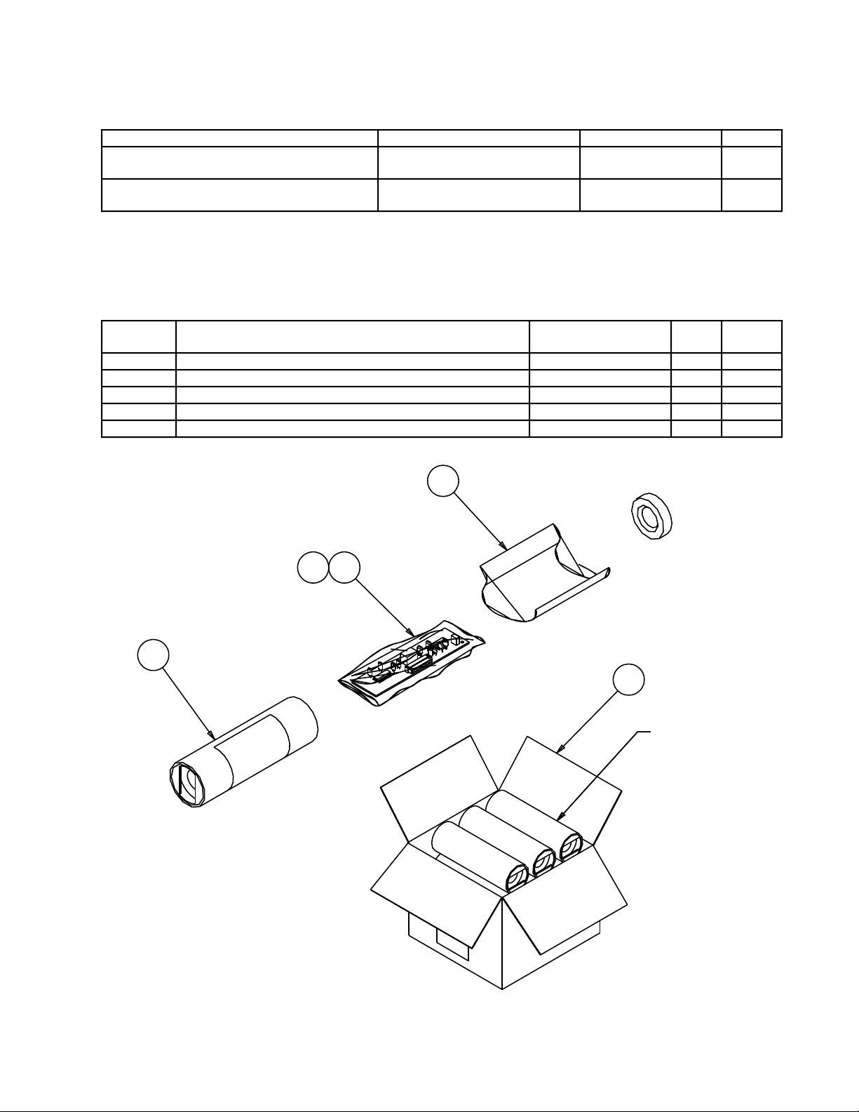
FREESPACE® MODEL 1B EQ CARD PART LIST
Miscellaneous
Reference Designator Description Part Number Note
S1 SWITCH, SPDT, VERT,
SLIDE
JP1 CONN, HEADER,
RTANG, 12 POS
PACKING LIST
FreeSpace Model 1B EQ card (see Figure 8)
187481
149538
Item
Number
1 OWNERS GUIDE, INST, EQ CARDS, PRO 191912 1
2 PCB ASSY, MODEL 1B EQ CARD 190671 1
3 BAG, ANTISTAT, 4X7.5 177761 1
4 TUBE, PACKING, ROUND, PLUG-SEAL 184177 1
5 CARTON, RSC, 9.63X7.88X6.63 178853 1
Description Part Number Qty. Note
1
2
3
4
5
REF (END CAP)
12 PACKAGED
EQ CARDS
PER CARTON
Figure 8. FreeSpace Model 1B EQ Card Packing View
41
Page 42

MODEL 8 EQ CARD PART LIST
Resistors
Reference Designator Description Part Number Note
R1 20.0 KΩ, 1206, 1/8W, 1% 124894-2002
R2 14.0 KΩ, 1206, 1/8W, 1% 124894-1402
R3, 13 4.12 KΩ, 1206, 1/8W, 1% 124894-4121
R5, 25 887 Ω, 1206, 1/8W, 1% 124894-8870
R9 11.5 KΩ, 1206, 1/8W, 1% 124894-1152
R11 110 KΩ, 1206, 1/8W, 1% 124894-1103
R12 100 KΩ, 1206, 1/8W, 1% 124894-1003
R14 16.5 KΩ, 1206, 1/8W, 1% 124894-1652
R16, 20 4.99 KΩ, 1206, 1/8W, 1% 124894-4991
R17, 22 7.15 KΩ, 1206, 1/8W, 1% 124894-7151
R18, 26 6.19 KΩ, 1206, 1/8W, 1% 124894-6191
R19 10.0 KΩ, 1206, 1/8W, 1% 124894-1002
R27 15.0 KΩ, 1206, 1/8W, 1% 124894-1502
R31 21.5 KΩ, 1206, 1/8W, 1% 124894-2152
R32 78.7 KΩ, 1206, 1/8W, 1% 124894-7872
R35, 36, 40, 41, 42, 43, 44, 45 JUMPER, CHIP 124896
R37, 38 47.0 KΩ, 1206, 1/8W, 5% 124895-4735
Capacitors
Reference Designator Description Part Number
C2, 8, 10 .047 uF, BOX, 85, 63V, 5% 137127-473
C3 .33 uF, BOX, 85, 50V, 5% 137127-334
C6 .0033 uF, BOX, 85, 100V,
5%
C11 .033 uF, BOX, 85, 63V, 5% 137127-333
C12 .0056 uF, BOX, 85, 100V,
5%
C20, 22 .022 uF, BOX, 85, 100V,
5%
C24, 26, 48, 49, 50, 51 10000 pF, CHIP, 5% 124959-103
C25 .0027 uF, BOX, 85, 100V,
5%
C27 .0022 uF, BOX, 85, 100V,
5%
Diodes
Reference Designator Description Part Number
D1, 2, 3, 5 1N4148, 52MM AXIAL 121501
D4, 6 ZEN, 18V, 1W, 5%,
1N4746
Integrated Circuits
137127-332
137127-562
137127-223
137127-272
137127-222
116995-4746A
Reference Designator Description Part Number
U1, 2 IC, OP AMP, QUAD 144008
U3 IC, SWITCH, ACTIVE,
SIP-8, BA3128N
42
177292
Page 43
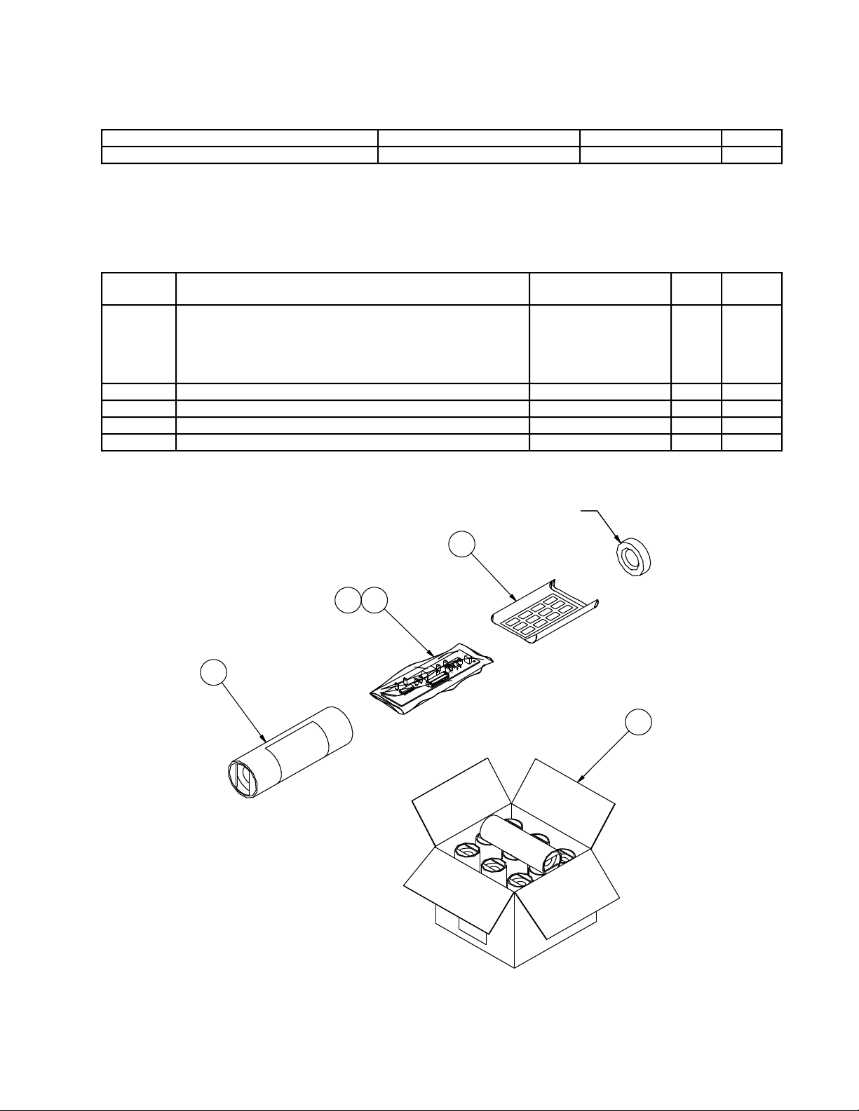
MODEL 8 EQ CARD PART LIST
Miscellaneous
Reference Designator Description Part Number
J1 CONN, HEADER, 12 PIN 149538
PACKING LIST
Model 8 EQ Card (see Figure 9)
Item
Number
1 LIT KIT, PRO EQ CARDS, 1800-V,#2
CONTAINS:
1. POLY BAG
2. INSTALLATION SHEET
3. LABELS, CHASSIS
2 PCB ASSY, M8 EQ CARD 184824 1
3 BAG, ANTISTAT, 4X7.5 177761 1
4 TUBE, PACKING, ROUND, PLUG-SEAL 184177 1
5 CARTON, RSC, 9.63X7.88X6.63 178853 1
Description Part Number Qty. Note
184815
178854
183746
184816
END CAP
1
23
4
1
1
1
1
Figure 9. Model 8 Equalizer PCB Packing View
43
5
Page 44
MODEL 25/32 EQ CARD PART LIST
Resistors
Reference Designator Description Part Number Note
R1 20.0 KΩ, 1206, 1/8W, 1% 124894-2002
R2, 16, 17 10.0 KΩ, 1206, 1/8W, 1% 124894-1002
R3, 14 22.1 KΩ, 1206, 1/8W, 1% 124894-2212
R5, 27 8.25 KΩ, 1206, 1/8W, 1% 124894-8251
R9 11.5 KΩ, 1206, 1/8W, 1% 124894-1152
R11 110 KΩ, 1206, 1/8W, 1% 124894-1103
R12 150 KΩ, 1206, 1/8W, 1% 124894-1503
R13, 20 4.99 KΩ, 1206, 1/8W, 1% 124894-4991
R18, 19 4.75 KΩ, 1206, 1/8W, 1% 124894-4751
R22 3.92 KΩ, 1206, 1/8W, 1% 124894-3921
R25, 35, 36, 40, 41, 42, 43, 44, 45 JUMPER, CHIP 124896
R26 6.19 KΩ, 1206, 1/8W, 1% 124894-6191
R31 21.5 KΩ, 1206, 1/8W, 1% 124894-2152
R32 78.7 KΩ, 1206, 1/8W, 1% 124894-7872
R37, 38 47.0 KΩ, 1206, 1/8W, 5% 124895-4735
Capacitors
Reference Designator Description Part Number Note
C2 .068 uF, BOX, 85, 63V, 5% 137127-683
C3 .27 uF, BOX, 85, 50V, 5% 137127-274
C8 .047 uF, BOX, 85, 63V, 5% 137127-473
C10 .056 uF, BOX, 85, 63V, 5% 137127-563
C11, 12 .0056 uF, BOX, 85, 100V,
5%
C20, 22 .022 uF, BOX, 85, 100V,
5%
C24, 26, 48, 49, 50, 51 10000 pF, CHIP, 5% 124959-103
C25, 27 .0027 uF, BOX, 85, 100V,
5%
Diodes
Reference Designator Description Part Number Note
D1, 2, 3, 5 1N4148, 52MM AXIAL 121501
D4, 6 ZEN, 18V, 1W, 5%,
1N4746
Integrated Circuits
Reference Designator Description Part Number Note
U1, 2 OP AMP, QUAD 144008
U3 SWITCH, ACTIVE, SIP-8,
BA3128N
137127-562
137127-223
137127-272
116995-4746A
177292
Miscellaneous
Reference Designator Description Part Number Note
J1 CONN, HEADER,
12 PIN
44
149538
Page 45

PACKING LIST
Model 25/32 EQ Card (see Figure 10)
Item
Number
1 LIT KIT, PRO EQ CARDS, 1800-V,#2
CONTAINS:
1. POLY BAG
2. INSTALLATION SHEET
3. LABELS, CHASSIS
2 PCB ASSY, M32 EQ CARD 183743 1
3 BAG, ANTISTAT, 4X7.5 177761 1
4 TUBE, PACKING, ROUND, PLUG-SEAL 184177 1
5 CARTON, RSC, 9.63X7.88X6.63 178853 1
Description Part Number Qty. Note
184815
178854
183746
184816
END CAP
1
23
1
1
1
1
4
5
Figure 10. Model 25/32 Equalizer PCB Packing View
45
Page 46

MAIN PART LIST
FreeSpace® Zone 2 Remote Control with A/B Switch (see Figure 11)
Item
Number
1 BAG, POLY, 9.38X6X2 mil 100278 1
2 SCREW, MACH, 6-32X1.00, OVAL
2 SCREW, MACH, M3.5X25MM, FLAT,
3 SW500 SWITCH, SPST, ROCKER 178108 1
4 KNOB, REMOTE, FREESPACE 6 178104 1
5 SCREW, TAPP, 6-13X.5, PAN, XREC 173555-08 2
6 R500 POT, RTRV, 10K OHM, 10% 177299-103 1
7 COVER, REMOTE, FREESPACE 6 178103 1 US/CA,
7 COVER, REMOTE, FREESPACE 6 178101 1 EU, UK
8 PCB ASSY, REM, BMS, VOL /AB 187982 1
9 CARTON, D/C, INTERLOCK, KIT 131843 1
2
Ref.
Des.
Description Part Number Qty. Note
178115-16 2 US/CA
HD
178116-25 2 EU, UK,
XREC
4
7
AUS
AUS
6
9
3
8
1
5
Figure 11. FreeSpace Zone 2 Remote Control with A/B Switch Exploded View
46
Page 47

MAIN PART LIST
FreeSpace® Zone 2 Remote Volume Control without A/B Switch (see Figure 12)
Item
Number
Description Part
Number
Qty. Note
1 PCB ASSY, REM, BMS, VOLUME 187983 1
2 WALLPLATE, RVC 188611 1 US, CA,
2 WALLPLATE, NO SWITCH, RVC 188610 1 EU, UK
3 KNOB, REMOTE, FREESPACE 6 178104 1
4 SCREW, MACH, 6-32x1, .00, OVAL HD 178115-16 2 US/CA
4 SCREW, MACH, M3, 5x25mm, FLAT, XREC 178116-25 2 EU, UK,
5 SCREW, TAPP, 6-13x.5, PAN, XREC 173555-08 2
6 BAG, POLY, 9.38x6x2 MIL 100278 1
7 CARTON, D/C, INTERLOCK KIT, CANN 131843 1
4
3
2
AUS
AUS
7
1
5
6
Figure 12. FreeSpace Zone 2 Remote Volume Control without A/B Switch Exploded View
47
Page 48

SIGNAL A
SIGNAL B
CONTROL B
CONTROL C
INTEGRATED CIRCUIT PINOUT DIAGRAMS
14
IN/OUT
OUT/IN
OUT/IN
IN/OUT
VSS
1
SW
A
2
3
SW
D
4
SW
5
6
B
SW
C
7
VDD
13
CONTROL A
12
CONTROL D
11
IN/OUT
10
OUT/IN
9
OUT/IN
8
IN/OUT
SIGNAL D
SIGNAL C
1
2
-+
3
4
5
-+
6
-+
-+
14
13
12
11
10
7 8
9
PIN FUNCTION
1. A OUTPUT
2. A -INPUT
3. A +INPUT
4. V+
5. B +INPUT
6. B -INPUT
7. B OUTPUT
8. C OUTPUT
9. C -INPUT
10. C +INPUT
11. V-
12. D +INPUT
13. D -INPUT
14. D OUTPUT
Bose
®
P/N: 119837, Device Type CD 4066B,
CMOS Quad Bilateral Switch
1
Y0
2
Y2
3
Y
4
Y3
5
Y1
6
INHIBIT
VEE
7
8 9
VSS
VDD
X2
X1
X0
X3
16
CONTROLS
15
14
X
13
12
SWITCHES
11
A
10
IN/OUT
B
Bose P/N's: 147243/187620, Device Type CD4052, Analog Multiplexer
8
Vcc
7
+IN B
+
-
6
- IN B
5
OUT
Bose P/N: 144008, Device Type NJM2059D,
Quad Op-Amp
6
10
9
12
14
15
11
1
5
2
4
TRACK TRIM A
RECOVERY CAP. A
RECTIFIER INPUT A
ATTACK CAP. A
Inhibit
A
B
X0
X1
X2
X3
Y0
Y1
Y2
Y3
X
VDD = PIN 16
VSS = PIN 8
VEE = PIN 7
Y
1
2
3
4
13
3
COMMONS
OUT/IN
16
15
14
13
VCC
TRACK TRIM B
RECOVERY CAP. B
RECTIFIER INPUT B
4
VEE
+
-
3
- IN A
2
+ IN A
1
SW
Bose P/N: 177292, Device Type NJM2120,
Dual Op-Amp with Active Switch
GAIN OUT A
THD TRIM A
GAIN INPUT A
GROUND
5
6
7
89
12
11
10
Bose P/N: 178894, Device Type NE572N,
Dual Channel Compander
48
ATTACK CAP. B
GAIN OUT B
THD TRIM B
GAIN INPUT B
Page 49

INTEGRATED CIRCUIT PINOUT DIAGRAMS
A
B
-+
-+
1
2
3
45
6
7
8
PIN FUNCTION
1. A OUTPUT
2. A -INPUT
3. A +INPUT
4. V-
5. B +INPUT
6. B -INPUT
7. B OUTPUT
8. V+
1
2
-+
3
4
5
-+
6
7 8
-+
-+
14
13
12
11
10
PIN FUNCTION
1. A OUTPUT
2. A -INPUT
3. A +INPUT
4. V+
5. B +INPUT
6. B -INPUT
7. B OUTPUT
8. C OUTPUT
9. C -INPUT
9
10. C +INPUT
11. V-
12. D +INPUT
13. D -INPUT
14. D OUTPUT
Bose P/N: 187472, Device Type NJM2059M,
Quad Op-Amp
A
1
B
2
J
3
K
4
C
5
D
6
VSS
7 8
14
13
12
11
10
VDD
H
G
M
L
9
F
E
Bose P/N: 188648, Device Type CD4001,
Quad 2-Input Nor Gate
Bose® P/N: 187473, Device Type NJM4559M,
Dual Op-Amp
1
2
3
4
+
-
+
A
5
6
7
16
15
14
13
-
B
12
11
10
98
Pin Configuration
1. Amp Bias Input A
2. Diode Bias A
3. + Input A
4. - Input A
5. Output A
6. V -
7. Buffer Input A
8. Buffer Output A
9. Buffer Output B
10. Buffer Input B
11. V +
12. Output B
13. - Input B
14. + Input B
15. Diode Bias B
16. Amp Bias Input B
Bose P/N: 188650, Device Type NJM13700,
Dual Transconductance Amplifier
49
Page 50

GENERAL TROUBLESHOOTING TIPS
Guidelines for wiring to and from the system electronics
• Always use shielded cable and follow the wiring diagrams in the Installer's Guide, Bose
number 191911.
• A cable with braided shield is preferable to one with a spiral or foil shield.
• Keep the input wiring distant from AC mains wiring.
• Keep the input wiring distant from loudspeaker wiring.
• Never bundle input and loudspeaker or power wiring together in the same jacket, or with
lacing twine, or in the same conduit.
• Do not connect the input signal grounds to either side of the loudspeaker output.
• Place the source equipment as close to the system electronics as practical to keep the
wiring short.
• Whenever possible, use source equipment with balanced outputs, and receive it at Music
Input A balanced.
• If the source equipment must be over 12 feet (4 m) away, and is unbalanced, equip it with a
balancing transformer to convert it to a balanced output.
®
part
• Note that in most of the wiring diagrams given in the Installer's Guide, Bose part number
191911, the shield of the cable is connected only at the source end. It is poor practice to
ground the shield at both ends, because then it serves as a conductor and radiates
interference into the center wires. With unbalanced sources and pre-wired RCA-RCA plug
cables, the shield is grounded at both ends. However, cables with two-conductor shielded
wire , using the two wires for hot and ground, and grounding the shield only at the source
end may perform better.
Balanced Source Terminals
• The signal outputs of equipment with balanced outputs consist of three terminals. The
positive (+), the negative (-), and the GND (or COMM or COM). The audio signal it applied
across the (+) and the (-) terminals as a voltage. The (+) and (-) outputs may or may not be
referenced to the GND terminal. The receiving equipment input, if balanced, should respond
only to the voltage difference between the (+) and (-) terminals. This leads to improved
rejection of interference picked up in the cable.
• Screw terminal - Each output of the source equipment has a positive (+), a negative
terminal (-), and a GND terminal. Connect the cable to these terminals. On some equipment,
a chassis ground screw or bolt may be found. Do not use this ground point as a signal
ground.
• Phone Connector - This connector will be 1/4 inch in diameter. The sleeve of the connector
is always used for GND. The tip carries the (+) side of the signal, and the ring carries the (-)
side of the signal.
50
Page 51

GENERAL TROUBLESHOOTING TIPS
Balanced Source Terminals (continued)
• XLR Connector - These are industry standard 3-pin connectors with a surrounding metal
shield. Pin 1 is always GND. Pin 3 is usually (+) and pin 2 is (-). Older equipment often
presents its outputs with pins 2 and 3 interchanged.
Unbalanced Source Terminals
• The signal outputs of equipment with unbalanced outputs consist of two terminals. The
positive (+) and the GND (or COMM or COM). The audio is applied across these terminals
as a voltage referenced to the GND terminal. There is no negative (-) terminal because it is
merged with the GND terminal.
• Unbalanced sources are less expensive to implement and are fine for situations where the
cable length needs to be short. If the interconnecting cable must be longer than 12 feet
(4 m), the source should have a balanced output. The reason is that unbalanced
connections are inherently more susceptible to the pickup of audio interference from AC
mains hum, RFI, and lighting dimmers.
• Typically, unbalanced sources have screw terminals, an RCA connector (also called a phono
connector), or a phone connector.
• Screw Terminal - Each output of the source equipment has a positive (+) terminal and a
GND terminal. Connect the cable to these terminals. On some equipment, a chassis ground
screw or bolt may be found. Do not use this point as a signal ground.
• RCA (phono) Connector - This connector accepts plugs with a center pin for the positive (+)
side of the signal, and a concentric shield for the GND side.
• Phone Connector - This connector comes in several styles. Some are mono (tip and sleeve);
others are stereo (tip, ring, and sleeve). Some are 1/4 inch in diameter, some are 1/8 inch in
diameter. The sleeve of the connector is always used for GND. The tip of the mono plug
carries the positive (+) side of the signal. In stereo usage, the tip is the left channel positive
(+) signal and the ring is the right channel positive (+) signal.
51
Page 52

TROUBLESHOOTING
The Opti-Voice® Page Option Card
Problem Possible Cause Solution
The audio signal
sounds distorted
The system sounds
noisy when the
page is triggered.
Paging is not audible
in the loudspeakers.
The gain levels are
set too high.
The gain levels are
set too low.
1. The page
assignment
switches are not set
properly.
Lower the gain level on the distorted
channels until the LED no longer flashes
red during loud passages. If necessary,
switch the internal microphone pad to the
0dB position.
Increase the gain levels on the noisy
channels until the gain LED flashes red.
Then lower the gain slightly until the LED
no longer flashes red. This will optimize
compressor operation and signal-to-noise
ratio.
1. Send your paging sources to the correct
listening zone. (see info on internal switch
settings).
Feedback occurs
during paging from a
microphone.
Sometimes the
music fades out
unexpectedly.
2. The page trigger
level is set too high.
3. The page level
trim is set too low.
1. There is too much
gain for the paging
signal.
2. Page microphone
is too close to one of
the loudspeakers.
1. The page trigger
is set too low.
2. The room's
ambient noise is too
loud.
2. Turn the page level trim to the right to
increase the sensitivity.
3. Turn the page level trim to the right to
increase the page level.
1. Reduce the gain with the page source
gain trim or the page level trim. If the OptiVoice compressor is enabled, try disabling
it.
2. Re-position the loudspeaker nearest to
the page microphone, or change the page
microphone to a type with a more
directional (cardiod) pickup pattern and
orient it away from the direction of the
nearest loudspeaker.
1. Increase the level at which paging
occurs by turning the page trigger level to
the left. (See making connections and
setting levels info).
2. Use a microphone with a push-to-talk
switch. This will eliminate false triggering of
the music mute due to high ambient noise
conditions.
52
Page 53

TROUBLESHOOTING
The Opti-Source™ Option Card
Problem Possible Cause Solution
The audio signal
sounds distorted.
The system sounds
noisy when the
music compressors
are engaged.
When using the
AUTO mode, the
"B" source interrupts
the "A" source
prematurely.
Quiet passages of
music are difficult to
hear.
One channel does
not switch when in
manual mode.
When the input
mode switch is in the
MONO position,
and the A/B mode
switch is in AUTO,
the "B" source does
not fade in smoothly
on channel 2.
The input switch on
the Opti-Source
card is in 2-ch mode,
but the "A" source
sounds like it is in
mono.
The gain levels are
set too high.
The gain levels are
set too low.
The wait delay is
too short.
The music
compressor has not
been enabled.
The Ch.1 and Ch.2
terminals have not
been jumpered at
the A/B Remote
Volume Control
inputs.
The input mode
switch position is
wrong. Auto
switching is not
available on Ch.2
when the input
mode switch on the
Opti-Source card is
in the MONO
position.
The input mode
switch on the
AmPlus™ 100
amplifier is in the
wrong position.
Lower the gain level on the distorted
channels until the gain LED no longer
flashes red during loud music passages.
Increase the gain levels on the noisy
channels until the gain LED flashes red.
This will optimize compressor operation
and signal-to-noise ratio.
Set the internal wait delay switch to a
longer delay time.
Enable the music compressor by using the
internal switches.
When using the Remote Volume Control to
A/B both channels simultaneously (one
zone applications), the remote control
inputs on the quick-connect terminal blocks
on the Opti-Source card must be tied
together.
Switch the input mode to 2-ch operation. In
addition, make sure a mono signal is being
applied to the inputs, or wire the signal for
mono at the inputs by tying the two inputs
together at the input connector.
Switch the input mode on the AmPlus 100
amplifier to 2-ch. This will preserve the
stereo signal being sent to the Opti-Source
card.
53
Page 54

Figure 14. FreeSpace Model 1B Equalizer Board SMD and Etch Layout Diagram
Figure 13. FreeSpace
®
Model 1B Equalizer Board Topside and Etch Layout Diagram
54
Page 55
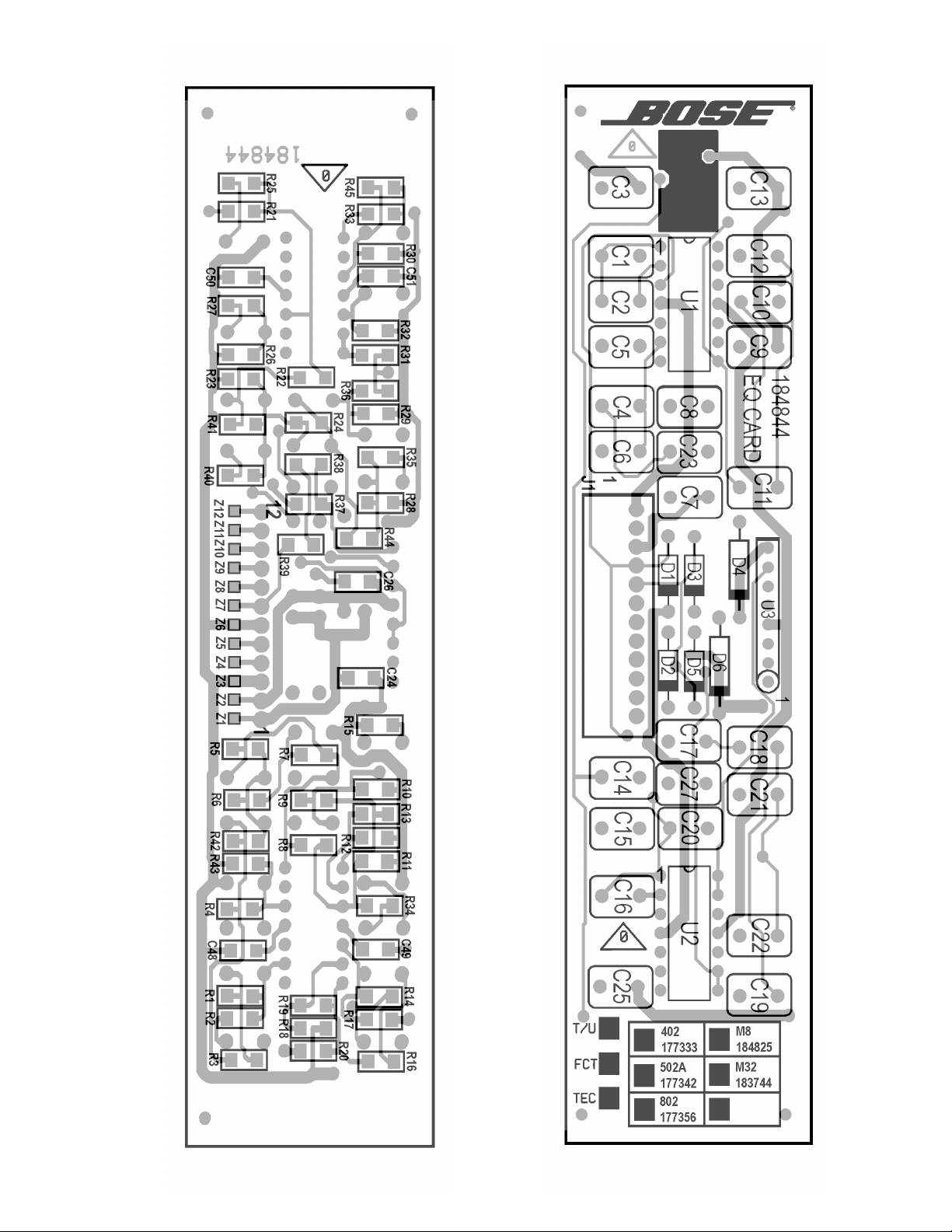
Figure 16. Models 8 and 25/32 SMD Component and Etch Layout Diagram
Figure 15. Models 8 and 25/32 Equalizer PCB Topside Component and Etch Layout Diagram
55
Page 56

A
B
C
Note: See the part list for the proper value of OPT components.
4.99k
R20
C14
R40
0
N.U.
78
OPT
Figure 17. Models 8 and 25/32 Equalizer PCB Schematic Diagram
.0027
6.19K
6
5
34
2
Model 8, and Model 25/32
EQ PCB 184844
Page 1 of 1
FRAMINGHAM, MA 01701-9168
R25
C25
R26
-15V
OPT
N.U.
78.7K
C16
N.U.
R27
.022
C20
R29
0
N.U.
C21
.022
C22
R32
12
13
RC4156N
U2
14
-15V
.01
R39
NU
J1
7
N.U.
R21
R41
C15
0
N.U.
R22
OPT
2
3
RC4156N
4
11
U2
C50
.01
C51
.01
1
R36
21.5K
R31
673
-INB
VEE
4
NJM2120
47k
R38
1N4148
1N4746A
SW
1
D5
D6
C26
-15V
+INB
J1-5
+15V
R23
N.U.
OPT
2
+INA
-INA
VCC
OUT
5
47k
N.U.
N.U.
R30
8
U3
R37
1N4148
1N4746A
R28
C27
9
D3
N.U.
N.U.
N.U.
N.U.
RC4156N
8
D4
R24
C17
R44
0
R35
0
C18
R45
N.U.
6
R33
RC4156N
U2
7
5
C19
0
10
U2
+15V
C24
.01
+15V
20k
OPT
R2
OPT
C3
R42
0
N.U.
N.U.
N.U.
C7
N.U.
8
J1-4
-15V
1N4148
D2
2
.068
R1
C2
C1
N.U.
C4
R6
OPT
OPT
R5
R7
N.U.
N.U.
C9
110K
R11
R12
OPT
OPT
R13
OPT
R14
C13
N.U.
R17
OPT
OPT
R18
OPT
R19
J1-6
J1-2
J1-3
J1-1
+15V
-15V
RC4156N
4
11
U1
C49
.01
1
OPT
R3
R43
0
N.U.
R4
N.U.
C5
6
5
RC4156N
U1
7
C6
.047
C8
R8
OPT
N.U.
C10
10
9
RC4156N
U1
8
OPT
C11
.0056
C12
OPT
13
12
RC4156N
U1
14
+15V
1N4148
D1
3
.01
C48
7
6
C23
N.U.
5
R34
N.U.
R10
11.5K
R9
4
R15
3
OPT
R16
2
1
R
A
B
C
DD
1
56
Page 57

AmPlus™ 50 and 100 Amplifier
®
®
Opti-Voice
®
and Opti-Source™
Option Cards
and
FreeSpace
®
Model 1B, Model 8
and Model 25/32 EQ Cards
©
1998 Bose Corporation
Supplement
Part Number 194101-S2 Rev. 00
Page 58

SPECIFICATIONS AND FEATURES SUBJECT TO CHANGE WITHOUT NOTICE
®
®
Bose Corporation
The Mountain
Framingham, Massachusetts USA 01701
P/N: 194101-S2 Rev. 00 4/98 FOR TECHNICAL ASSISTANCE OR PART ORDERS, CALL 1-800-367-4008
 Loading...