

Page 1
©2012 Bose Corporation
Reference Number 273029-SM Rev. 12
Service Manual
3•2•1, 3•2•1GS and 3•2•1GSX Series II
Home Entertainment Systems
(US and non-US Standard and Premium Versions)
Electronic Copy Only
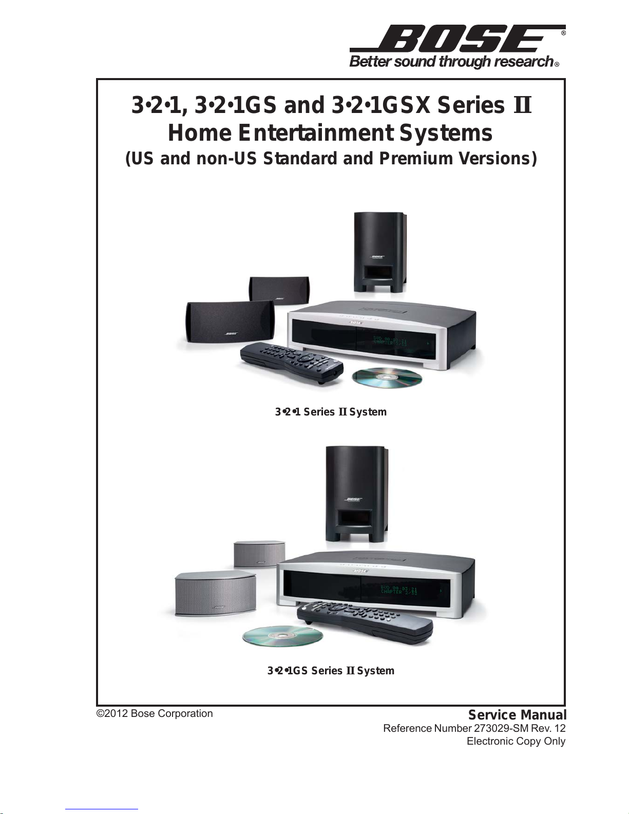
3•2•1 Series II System
3
•2•1GS Series II System
Page 2
2
CONTENTS
Safety Information ...................................................................................................................................3
Warranty ....................................................................................................................................................3
Product Description ................................................................................................................................4
Accessories..............................................................................................................................................4
Specifications:...................................................................................................................................... 5-8
Electrostatic Discharge Sensitive (ESDS) Device Handling ............................................................ 9
Part List Notes ..........................................................................................................................................9
Packaging Part List, 3•2•1 Series II Home Entertainment System (see Figure 1) ................. 10-11
Figure 1. 3•2•1 Series II Home Entertainment System Packaging View ............................................... 11
Packaging Part List, 3•2•1 Series II System Accessory Kit (see Figure 2) ...................................12
Figure 2. Accessory Kit Exploded View ..................................................................................................12
Main Part List, 3•2•1 II and 3•2•1GS II Console Assembly (see Figure 3) ..................................... 1 3
Figure 3. 3•2•1 Series II Standard Console Exploded View .................................................................. 14
Main Part List, 3•2•1GSX Console Assembly (see Figure 4)........................................................... 15
Figure 4. 3•2•1GSX Series II Premium Console Exploded View ............................................................ 16
Main Part List, Bass Module (see Figure 5)......................................................................................17
Figure 5a. Bass Module Exploded View (units built before 4/27/09) ....................................................17
Figure 5b. Bass Module Exploded View (units built after 4/27/09) ....................................................... 18
Main Part List, Standard 3•2•1 Array Assembly (see Figure 6) .......................................................19
Figure 6. Standard 3•2•1 Array Assembly Exploded View ..................................................................... 19
Main Part List, 3•2•1 GS Array Assembly (see Figure 7) .................................................................. 20
Figure 7. 3•2•1 GS Array Assembly Exploded View .............................................................................. 20
Electrical Part Lists ......................................................................................................................... 21-46
Console Main PCB Assembly......................................................................................................... 21-34
Console Tuner PCB Assembly ....................................................................................................... 35-38
Bass Module DSP/Amplifier PCB Assembly ................................................................................. 39-45
Bass Module Input/Output PCB Assembly ........................................................................................46
Disassembly Procedures ............................................................................................................... 47-53
Console Procedures ....................................................................................................................... 47-50
Bass Module Procedures .............................................................................................................. 51-52
Disassembly Procedures .....................................................................................................................53
Standard Satellite Array Procedures ..................................................................................................53
Gemstone Satellite Array Procedures ...............................................................................................53
Test Procedures .............................................................................................................................. 5
4-63
Console Procedures ....................................................................................................................... 54-61
Bass Module Procedures ....................................................................................................................62
Satellite Array Procedures ...................................................................................................................63
Figure 8. 3•2•1 Series II Console Test Setup Diagram.......................................................................... 65
Figure 9. 3•2•1 Series II Bass Module Test Setup Diagram .................................................................. 66
Computer Setup Procedure .......................................................................................................... 67-68
TAP Cable Construction ........................................................................................................................69
Bass Module Test Cable Construction ..............................................................................................70
Console Test Cable Construction .......................................................................................................71
Putting the Console into TAP mode ....................................................................................................72
Console TAP Commands................................................................................................................. 72-75
Changing the Region Code .................................................................................................................76
Obtaining System Information from the Media Center Display ............................................... 77-78
DVD Lock options ..................................................................................................................................79
3•2•1 Series II System Date of Manufacture Information ................................................................80
IC Diagrams ....................................................................................................................................... 81-90
Troubleshooting .............................................................................................................................. 91-92
Glossary of Terms..................................................................................................................................93
Service Manual Revision History .......................................................................................................94
Page 3
3
SAFETY INFORMATION
1. Parts that have special safety characteristics are identified by the symbol on schematics
or by special notes on the parts list. Use only replacement parts that have critical characteristics
recommended by the manufacturer.
2. Make leakage current or resistance measurements to determine that exposed parts are
acceptably insulated from the supply circuit before returning the unit to the customer.
Use the following checks to perform these measurements:
A. Leakage Current Hot Check-With the unit completely reassembled, plug the AC line cord
directly into a 120V AC outlet. (Do not use an isolation transformer during this test.) Use a
leakage current tester or a metering system that complies with American National Standards
Institute (ANSI) C101.1 "Leakage Current for Appliances" and Underwriters Laboratories (UL)
UL6500 / UL60065 / IEC 60065 paragraph 9.1.1. With the unit AC switch first in the ON position
and then in OFF position, measure from a known earth ground (metal waterpipe, conduit, etc.)
to all exposed metal parts of the unit (antennas, handle bracket, metal cabinet, screwheads,
metallic overlays, control shafts, etc.), especially any exposed metal parts that offer an electrical
return path to the chassis. Any current measured must not exceed 0.5 milliamp. Reverse the
unit power cord plug in the outlet and repeat test. ANY MEASUREMENTS NOT WITHIN THE
LIMITS SPECIFIED HEREIN INDICATE A POTENTIAL SHOCK HAZARD THAT MUST BE
ELIMINATED BEFORE RETURNING THE UNIT TO THE CUSTOMER.
B. Insulation Resistance Test Cold Check-(1) Unplug the power supply and connect a jumper
wire between the two prongs of the plug. (2) Turn on the power switch of the unit. (3) Measure
the resistance with an ohmmeter between the jumpered AC plug and each exposed metallic
cabinet part on the unit. When testing 3 wire products, the resistance measured to the product
enclosure should be between 2 and infinite MOhms. Also, the resistance measured to exposed
input/output connectors should be between 4 and infinite MOhms. When testing 2 wire prod-
ucts, the resistance measured to exposed input/output connectors should be between 4 and
infinite MOhms. If it is not within the limits specified, there is the possibility of a shock hazard,
and the unit must be repaired and rechecked before it is returned to the customer.
CAUTION: The Bose® 3•2•1 Series II Home Entertainment System
contains no user-serviceable parts. To prevent warranty infractions,
refer servicing to warranty service stations or factory service.
PROPRIETARY INFORMATION
THIS DOCUMENT CONTAINS PROPRIETARY INFORMATION OF
BOSE CORPORATION WHICH IS BEING FURNISHED ONLY FOR
THE PURPOSE OF SERVICING THE IDENTIFIED BOSE PRODUCT
BY AN AUTHORIZED BOSE SERVICE CENTER OR OWNER OF
THE BOSE PRODUCT, AND SHALL NOT BE REPRODUCED OR
USED FOR ANY OTHER PURPOSE.
The Bose
®
3•2•1 and 3•2•1GS Series II Home Entertainment Systems are covered by a limited
1-year transferable warranty.
WARRANTY
Page 4
4
Overview:
The 3•2•1 Series II Home Entertainment Systems are the replacements for the 3•2•1 and
3•2•1GS Series I Home Entertainment Systems. They use the same system concept of a
console with a dedicated bass module with TrueSpace
TM
signal processed surround sound from
2 satellite arrays.
The 3•2•1 Series II product line consists of three total systems, the 3•2•1 Series II and 3•2•1GS
Series II systems, and the 3•2•1GSX system. There are a few differences between these
systems. The 3•2•1 Series II and the 3•2•1GS Series II system consoles do not contain a hard
disc drive. The 3•2•1GSX console contains a hard disc drive with uMusic functionality. Refer to
the system components listing below.
The 3•2•1 Series II system uses the standard, non-hard drive version of the console with graph-
ite cloth covered full size array speakers. The 3•2•1GS Series II systems use the standard non-
hard drive console with either graphite or silver metal grille array speakers with a silver or
graphite array cable. These arrays are smaller than the non-GS arrays.
Both the standard and premium consoles will play video DVDs, DVD-R and DVD+R discs, audio
CDs, Video CDs, CD-R and CD-RWs, and MP3 CDs. MP3 disc tracks must be burned in a
single closed session. The MP3 disc format must be ISO9660 and each file must have an
“.mp3” extension and have no other periods in the filename. The 3•2•1GSX system premium
console will also play stored music in the form of MP3 files stored on the hard disc drive.
There is only one version of the bass module. The bass module electronics house some signal
processing, power supplies and amplification for the console. The console and bass module are
not compatible with the 3•2•1 Series I console and bass module. They cannot be used to re-
place the other Series components. The speaker arrays are the same as currently used on the
3•2•1 and 3•2•1GS systems. The systems includes an enhanced universal type IR remote
control similar to that used on the 3•2•1GS Series I system. The uMusic remote used with the
321GSX has buttons to control the uMusic funtionality of the hard disc drive in the premium
console. These remotes are non-repairable.
System Components:
321 Series II Standard Console
Standard Graphite (cloth grilled) Arrays
Bass Module
Standard Remote Control
321GS Series II Standard Console
GS Arrays, silver or graphite, and color matching array cable
Bass Module
Standard Remote Control
321GSX Premium Console with HDD
GS Arrays, silver or graphite, and color matching array cable
Bass Module
uMusic Remote Control
PRODUCT DESCRIPTION
ACCESSORIES
The Bose 3•2•1 and 3•2•1GS Series II Home Entertainment Systems shelf speakers are com-
patible with Bose mounting accessories, including the UB-20 wall brackets, UFS-20 floor stands
and UTS-20 table stands.
Page 5
5
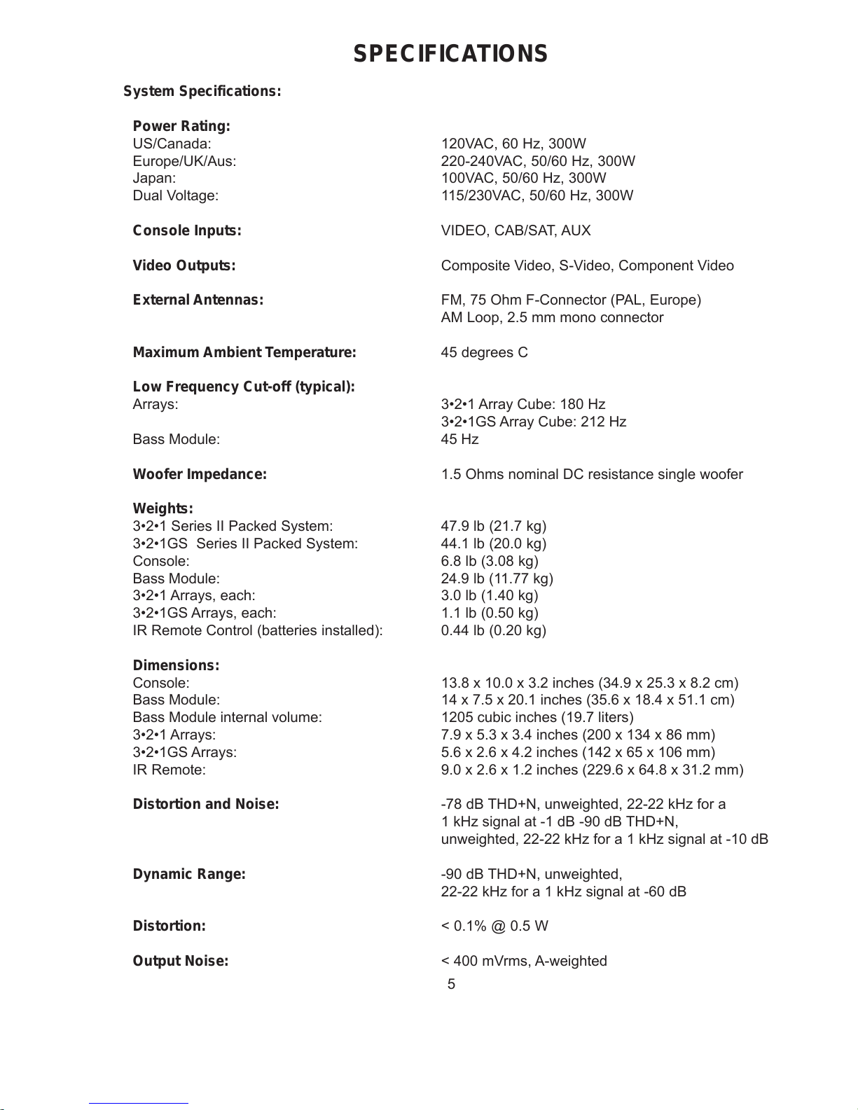
SPECIFICATIONS
System Specifications:
Power Rating:
US/Canada: 120VAC, 60 Hz, 300W
Europe/UK/Aus: 220-240VAC, 50/60 Hz, 300W
Japan: 100VAC, 50/60 Hz, 300W
Dual Voltage: 115/230VAC, 50/60 Hz, 300W
Console Inputs: VIDEO, CAB/SAT, AUX
Video Outputs: Composite Video, S-Video, Component Video
External Antennas: FM, 75 Ohm F-Connector (PAL, Europe)
AM Loop, 2.5 mm mono connector
Maximum Ambient Temperature: 45 degrees C
Low Frequency Cut-off (typical):
Arrays: 3•2•1 Array Cube: 180 Hz
3•2•1GS Array Cube: 212 Hz
Bass Module: 45 Hz
Woofer Impedance: 1.5 Ohms nominal DC resistance single woofer
Weights:
3•2•1 Series II Packed System: 47.9 lb (21.7 kg)
3•2•1GS Series II Packed System: 44.1 lb (20.0 kg)
Console: 6.8 lb (3.08 kg)
Bass Module: 24.9 lb (11.77 kg)
3•2•1 Arrays, each: 3.0 lb (1.40 kg)
3•2•1GS Arrays, each: 1.1 lb (0.50 kg)
IR Remote Control (batteries installed): 0.44 lb (0.20 kg)
Dimensions:
Console: 13.8 x 10.0 x 3.2 inches (34.9 x 25.3 x 8.2 cm)
Bass Module: 14 x 7.5 x 20.1 inches (35.6 x 18.4 x 51.1 cm)
Bass Module internal volume: 1205 cubic inches (19.7 liters)
3•2•1 Arrays: 7.9 x 5.3 x 3.4 inches (200 x 134 x 86 mm)
3•2•1GS Arrays: 5.6 x 2.6 x 4.2 inches (142 x 65 x 106 mm)
IR Remote: 9.0 x 2.6 x 1.2 inches (229.6 x 64.8 x 31.2 mm)
Distortion and Noise: -78 dB THD+N, unweighted, 22-22 kHz for a
1 kHz signal at -1 dB -90 dB THD+N,
unweighted, 22-22 kHz for a 1 kHz signal at -10 dB
Dynamic Range: -90 dB THD+N, unweighted,
22-22 kHz for a 1 kHz signal at -60 dB
Distortion: < 0.1% @ 0.5 W
Output Noise: < 400 mVrms, A-weighted
Page 6
6
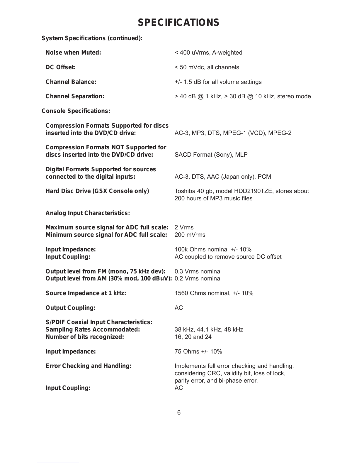
System Specifications (continued):
Noise when Muted: < 400 uVrms, A-weighted
DC Offset: < 50 mVdc, all channels
Channel Balance: +/- 1.5 dB for all volume settings
Channel Separation: > 40 dB @ 1 kHz, > 30 dB @ 10 kHz, stereo mode
Console Specifications:
Compression Formats Supported for discs
inserted into the DVD/CD drive: AC-3, MP3, DTS, MPEG-1 (VCD), MPEG-2
Compression Formats NOT Supported for
discs inserted into the DVD/CD drive: SACD Format (Sony), MLP
Digital Formats Supported for sources
connected to the digital inputs: AC-3, DTS, AAC (Japan only), PCM
Hard Disc Drive (GSX Console only) Toshiba 40 gb, model HDD2190TZE, stores about
200 hours of MP3 music files
Analog Input Characteristics:
Maximum source signal for ADC full scale: 2 Vrms
Minimum source signal for ADC full scale: 200 mVrms
Input Impedance: 100k Ohms nominal +/- 10%
Input Coupling: AC coupled to remove source DC offset
Output level from FM (mono, 75 kHz dev): 0.3 Vrms nominal
Output level from AM (30% mod, 100 dBuV): 0.2 Vrms nominal
Source Impedance at 1 kHz: 1560 Ohms nominal, +/- 10%
Output Coupling: AC
S/PDIF Coaxial Input Characteristics:
Sampling Rates Accommodated: 38 kHz, 44.1 kHz, 48 kHz
Number of bits recognized: 16, 20 and 24
Input Impedance: 75 Ohms +/- 10%
Error Checking and Handling: Implements full error checking and handling,
considering CRC, validity bit, loss of lock,
parity error, and bi-phase error.
Input Coupling: AC
SPECIFICATIONS
Page 7
7
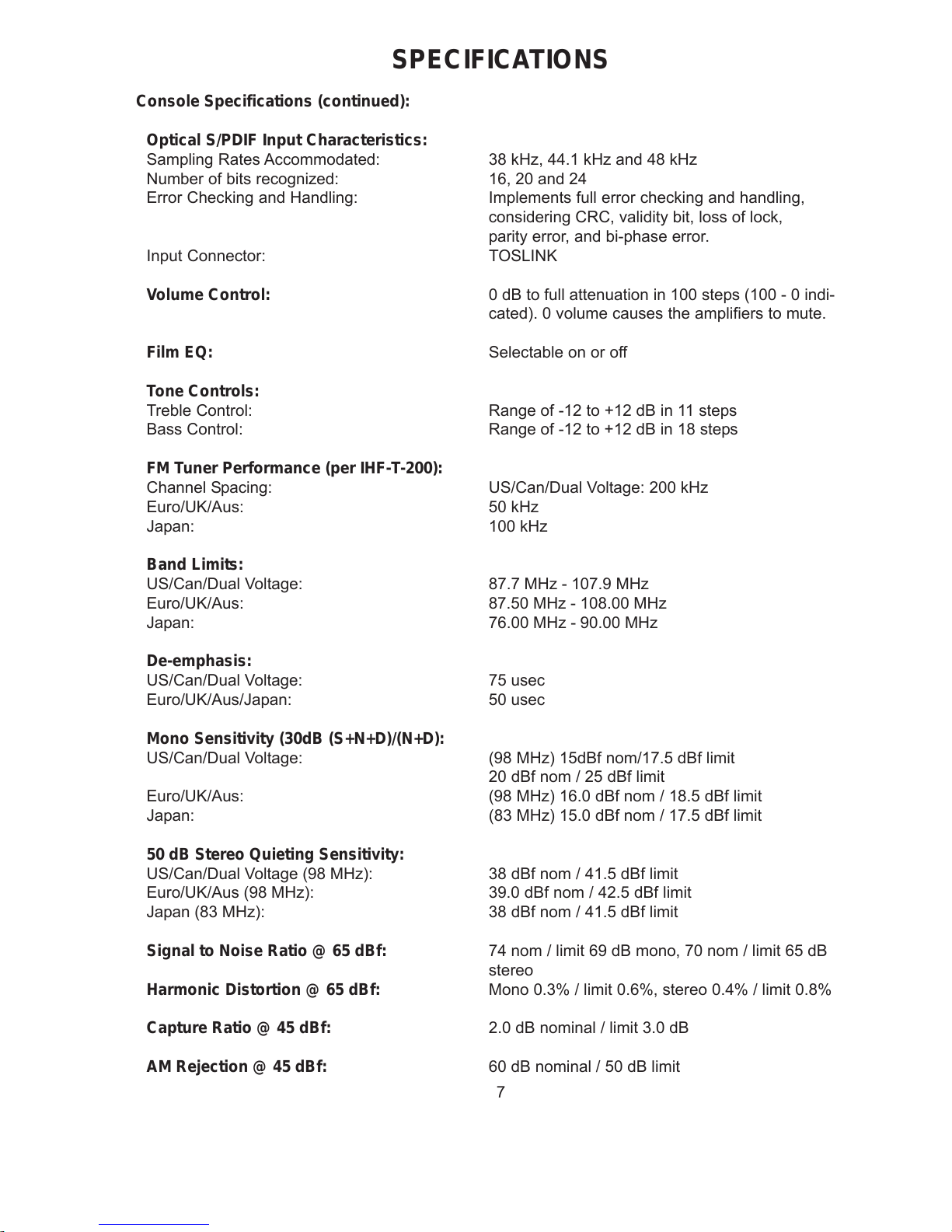
Console Specifications (continued):
Optical S/PDIF Input Characteristics:
Sampling Rates Accommodated: 38 kHz, 44.1 kHz and 48 kHz
Number of bits recognized: 16, 20 and 24
Error Checking and Handling: Implements full error checking and handling,
considering CRC, validity bit, loss of lock,
parity error, and bi-phase error.
Input Connector: TOSLINK
Volume Control: 0 dB to full attenuation in 100 steps (100 - 0 indi-
cated). 0 volume causes the amplifiers to mute.
Film EQ: Selectable on or off
Tone Controls:
Treble Control: Range of -12 to +12 dB in 11 steps
Bass Control: Range of -12 to +12 dB in 18 steps
FM Tuner Performance (per IHF-T-200):
Channel Spacing: US/Can/Dual Voltage: 200 kHz
Euro/UK/Aus: 50 kHz
Japan: 100 kHz
Band Limits:
US/Can/Dual Voltage: 87.7 MHz - 107.9 MHz
Euro/UK/Aus: 87.50 MHz - 108.00 MHz
Japan: 76.00 MHz - 90.00 MHz
De-emphasis:
US/Can/Dual Voltage: 75 usec
Euro/UK/Aus/Japan: 50 usec
Mono Sensitivity (30dB (S+N+D)/(N+D):
US/Can/Dual Voltage: (98 MHz) 15dBf nom/17.5 dBf limit
20 dBf nom / 25 dBf limit
Euro/UK/Aus: (98 MHz) 16.0 dBf nom / 18.5 dBf limit
Japan: (83 MHz) 15.0 dBf nom / 17.5 dBf limit
50 dB Stereo Quieting Sensitivity:
US/Can/Dual Voltage (98 MHz): 38 dBf nom / 41.5 dBf limit
Euro/UK/Aus (98 MHz): 39.0 dBf nom / 42.5 dBf limit
Japan (83 MHz): 38 dBf nom / 41.5 dBf limit
Signal to Noise Ratio @ 65 dBf: 74 nom / limit 69 dB mono, 70 nom / limit 65 dB
stereo
Harmonic Distortion @ 65 dBf: Mono 0.3% / limit 0.6%, stereo 0.4% / limit 0.8%
Capture Ratio @ 45 dBf: 2.0 dB nominal / limit 3.0 dB
AM Rejection @ 45 dBf: 60 dB nominal / 50 dB limit
SPECIFICATIONS
Page 8
8
SPECIFICATIONS
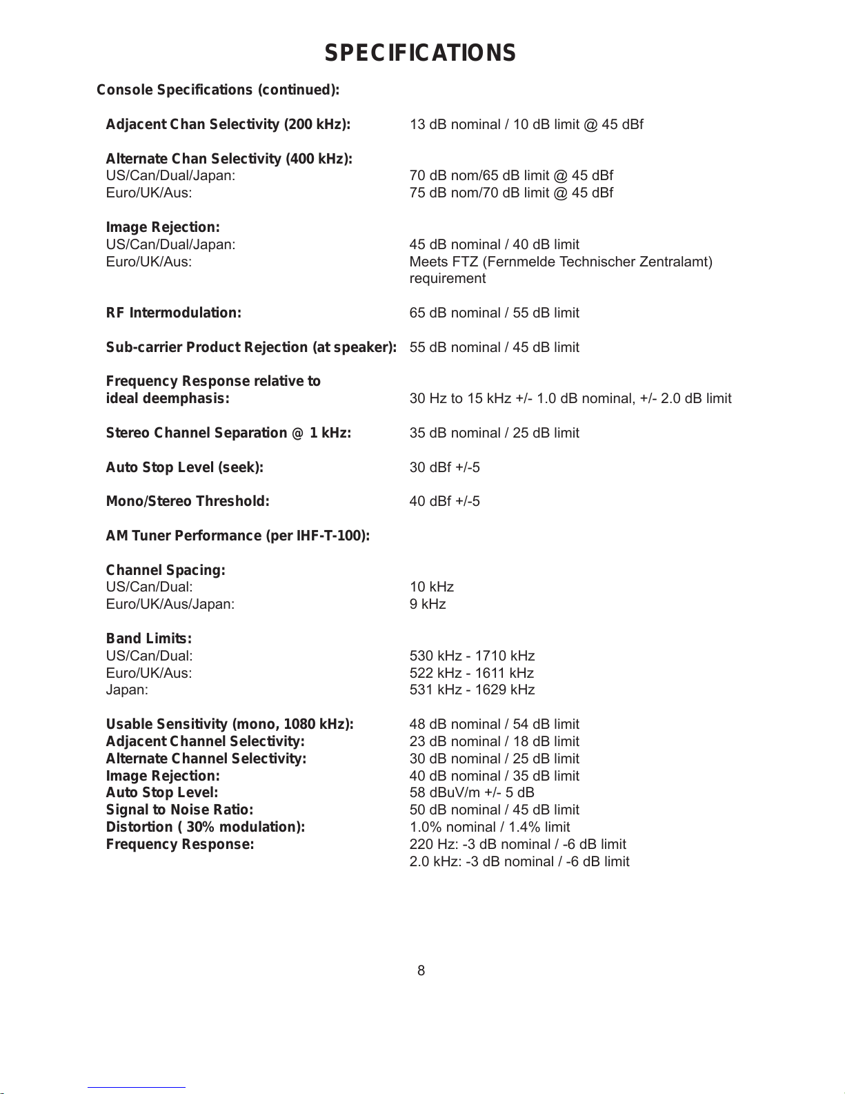
Console Specifications (continued):
Adjacent Chan Selectivity (200 kHz): 13 dB nominal / 10 dB limit @ 45 dBf
Alternate Chan Selectivity (400 kHz):
US/Can/Dual/Japan: 70 dB nom/65 dB limit @ 45 dBf
Euro/UK/Aus: 75 dB nom/70 dB limit @ 45 dBf
Image Rejection:
US/Can/Dual/Japan: 45 dB nominal / 40 dB limit
Euro/UK/Aus: Meets FTZ (Fernmelde Technischer Zentralamt)
requirement
RF Intermodulation: 65 dB nominal / 55 dB limit
Sub-carrier Product Rejection (at speaker): 55 dB nominal / 45 dB limit
Frequency Response relative to
ideal deemphasis: 30 Hz to 15 kHz +/- 1.0 dB nominal, +/- 2.0 dB limit
Stereo Channel Separation @ 1 kHz: 35 dB nominal / 25 dB limit
Auto Stop Level (seek): 30 dBf +/-5
Mono/Stereo Threshold: 40 dBf +/-5
AM Tuner Performance (per IHF-T-100):
Channel Spacing:
US/Can/Dual: 10 kHz
Euro/UK/Aus/Japan: 9 kHz
Band Limits:
US/Can/Dual: 530 kHz - 1710 kHz
Euro/UK/Aus: 522 kHz - 1611 kHz
Japan: 531 kHz - 1629 kHz
Usable Sensitivity (mono, 1080 kHz): 48 dB nominal / 54 dB limit
Adjacent Channel Selectivity: 23 dB nominal / 18 dB limit
Alternate Channel Selectivity: 30 dB nominal / 25 dB limit
Image Rejection: 40 dB nominal / 35 dB limit
Auto Stop Level: 58 dBuV/m +/- 5 dB
Signal to Noise Ratio: 50 dB nominal / 45 dB limit
Distortion ( 30% modulation): 1.0% nominal / 1.4% limit
Frequency Response: 220 Hz: -3 dB nominal / -6 dB limit
2.0 kHz: -3 dB nominal / -6 dB limit
Page 9
9
PART LIST NOTES
1. This part is not normally available from Customer Service. Approval from the Field Service
Manager is required before ordering.
2. The individual parts located on the PCBs are listed in the Electrical Part List.
3. This part is critical for safety purposes. Failure to use a substitute replacement with the
same safety characteristics as the recommended replacement part might create shock, fire
and/or other hazards.
4. This part is referenced for informational purposes only. It is not stocked as a repair part. Refer
to the next higher assembly for a replacement part.
ELECTROSTATIC DISCHARGE SENSITIVE (ESDS)
DEVICE HANDLING
This unit contains ESDS devices. We recommend the following precautions when repairing,
replacing or transporting ESDS devices:
• Perform work at an electrically grounded work station.
• Wear wrist straps that connect to the station or heel straps that connect to conductive
floor mats.
• Avoid touching the leads or contacts of ESDS devices or PC boards even if properly
grounded. Handle boards by the edges only.
• Transport or store ESDS devices in ESD protective bags, bins, or totes. Do not insert
unprotected devices into materials such as plastic, polystyrene foam, clear plastic bags,
bubble wrap or plastic trays.
Page 10
10
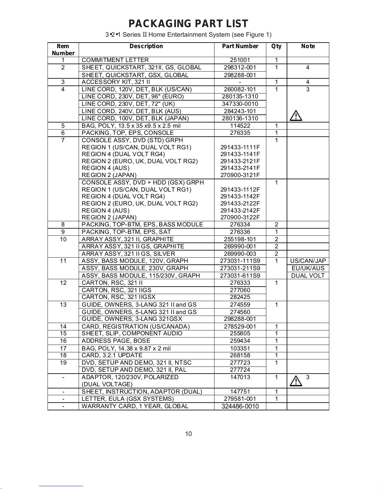
PACKAGING PART LIST
3•2•1 Series II Home Entertainment System (see Figure 1)
Item
Number
Description Part Number Qty Note
1 COMMITMENT LETTER 251001 1
2 SHEET, QUICKSTART, 321II, GS, GLOBAL 298312-001 1 4
SHEET, QUICKSTART, GSX, GLOBAL 298288-001
3 ACCESSORY KIT, 321 II - 1 4
4 LINE CORD, 120V, DET, BLK (US/CAN) 260082-101 1 3
LINE CORD, 230V, DET, 96" (EURO) 280135-1310
LINE CORD, 230V, DET, 72" (UK) 347330-0010
LINE CORD, 240V, DET, BLK (AUS) 284243-101
LINE CORD, 100V, DET, BLK (JAPAN) 280136-1310
5 BAG, POLY, 13.5 x 35 x9.5 x 2.5 mil 114522 1
6 PACKING, TOP, EPS, CONSOLE 276335 1
7 CONSOLE ASSY, DVD (STD) GRPH 1
REGION 1 (US/CAN, DUAL VOLT RG1) 291433-1111F
REGION 4 (DUAL V OLT RG4) 291433-1141F
REGION 2 (EURO, UK, DUAL VOLT RG2) 291433-2121F
REGION 4 (AUS ) 291433-2141F
REGION 2 (JAPAN) 270900-3121F
CONSOLE ASSY, DVD + HDD (GSX) GRPH 1
REGION 1 (US/CAN, DUAL VOLT RG1) 291433-1112F
REGION 4 (DUAL V OLT RG4) 291433-1142F
REGION 2 (EURO, UK, DUAL VOLT RG2) 291433-2122F
REGION 4 (AUS ) 291433-2142F
REGION 2 (JAPAN) 270900-3122F
8 PACKING, TOP-BTM, EPS, BASS MODULE 276334 2
9 PACKING, TOP-BTM, EPS, SAT 276336 1
10
A
RRA Y ASS Y, 321 II, GRAPHITE 255198-101 2
ARRAY ASSY, 321 II GS, GRAPHITE 269990-001 2
ARRAY ASSY, 321 II GS, SILVE R 269990-003 2
11 ASSY, BASS MODULE, 120V, GRAPH 273031-111S9 1 US/CAN/JAP
ASSY, BASS MODULE, 230V, GRAPH 273031-211S9 EU/UK/AUS
A
SSY, BASS MODULE, 115/230V, GRAPH 273031-611S9 DUAL VOLT
12 CARTON, RSC, 321 II 276333 1
CARTON, RSC, 321 IIGS 277060
CARTON, RSC, 321 IIGSX 282425
13 GUIDE, OWNERS, 3-LANG 321 II and GS 274559 1
GUIDE, OWNERS, 5-LANG 321 II and GS 274560
GUIDE, OWNERS, 3-LANG 321GSX 298288-001
14 CARD, REGISTRATION (US/CANADA) 278529-001 1
15 SHEET, SLIP, COMPONENT AUDIO 255805 1
16 A DDRESS PAGE, BOSE 259434 1
17 BAG, POLY, 14.38 x 9.87 x 2 mil 103351 1
18 CARD, 3.2.1 UPDATE 268158 1
19 DVD, SETUP AND DEMO, 321 II, NTSC 277723 1
DVD, SETUP AND DEMO, 321 II, PAL 277724
- ADAPTOR, 120/230V, POLARIZED
(DUAL VOLTAGE)
147013 1 3
- SHEET, INSTRUCTION, ADAPTOR (DUAL) 147751 1
- LETTER, EULA (GSX SYSTEMS) 279581-001 1
- WARRANTY CARD, 1 YEAR, GLOBAL
324486-0010
Page 11
11
Figure 1. 3
•2•1 Series II Home Entertainment System Packaging View
1
2
3
4
5
6
7
8
910
11
12
13 14 15 16 17 18
8
19
ARRAYS (ITEM 10)
INSIDE EPS FOAM
PACKAGING PART LIST
3•2•1 Series II Home Entertainment System, continued (see Figure 1)
Page 12
12
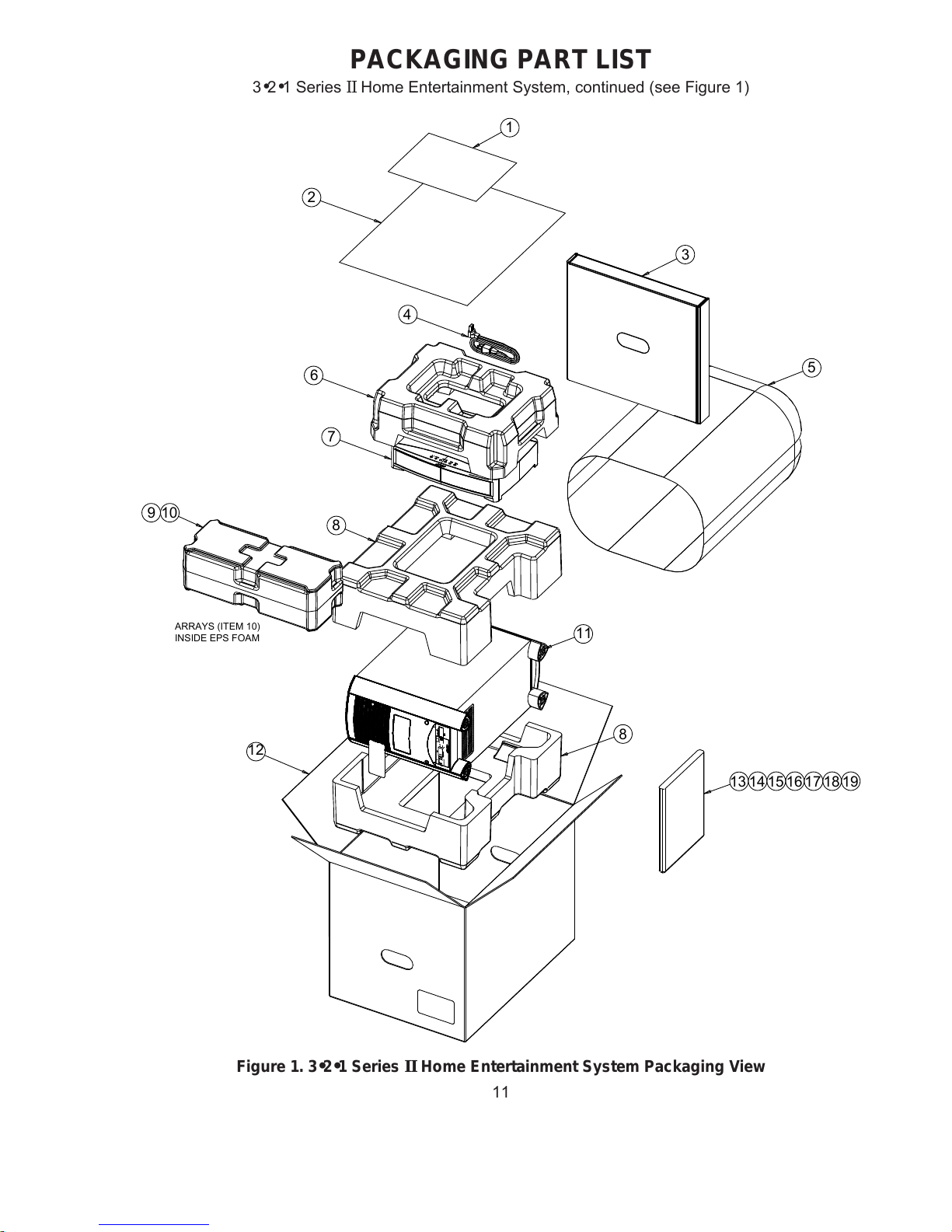
Figure 2. Accessory Kit Exploded View
PACKAGING PART LIST
3•2•1 Series II Home Entertainment System Accessory Kit (see Figure 2)
1
2
3
4
5
6
7
8
9
10
11
12
13
Item
Number
Description Part Number Note
1 CARTON, DI E CUT, ACCESSORY KIT , 32 1 II 276337
2
CABLE, AUD IO, DUAL RCA 185931-101
3
A
NTENNA, FM DIPOLE, 75 OHM, F CONN
(
US/CAN, JAPAN, DUAL RG1)
347426-0010
ANTENNA, FM, DIPOLE, PAL CONN
(EURO, UK, AUS, DUAL RG2 & RG4)
347423-0010
4 CABLE, VIDEO, 6', YL 3 47428-0010
5 REMOTE, IR, ADVANCED, 321 II / 32 1GS II
(PREPACKAGED REMOTE, BOSE P/N: 327236-0010)
288579-201 US/CAN
REMOT E, IR, ADVANCED, 321 II / 321GS II 288579-202 EURO/UK/AUS
REMOTE, IR, 321 II AND 321GS II 288579-203 JAPAN
REMOTE, IR, ADVANCED, 321G SX II
(PREPACKAGED REMOTE, BOSE P/N: 327236-1010)
288579-211 US/CAN
REMOTE, IR, ADVANCED, 321G SX II 288579-222 EURO/UK/AUS
REMOTE, IR, 321GSX II 288579-233 JAPAN
6
A
NTENNA, ASSY, AM, CD 20 199824-002
7 BAG, POLY, 4 x 6 x 2 mil 143393 4
8 BATTERY, CARBON, AA SIZE 147538
9 C ABLE, 15 FT , STA NDA R D A RR AY, 9 PIN , GR PH 255123-101
CABLE, 15 FT, GEMSTONETM ARRAY, 9 PIN, GRPH 269984-101
CABLE, 15 FT, GEMSTONE ARRAY, 9 PIN, SILVER 269984-103
10 BUMPER, RECESSED, FOOT, .88" 142839
11 FOOT, CLEAR, .312 X 0.85 178321-04
12 CABLE, B ASS MODU LE, 13 PIN, GRAPHITE, 10 FT 281528 -10 11
13 PACKING, INSERT, ACCESSORY KIT, 321 II 276338
CABLE, BASS MODU LE, 13 PI N, GRA PHITE, 25 FT 2 815 28- 10 01 SE RV IC E PART
- C A BLE, 40 FT, S TA NDAR D A RR A Y, 9 PIN , GR A PH
CABLE, 40 FT, GEMSTONE ARRAY, 9 PIN, GRAPH
CABLE, 40 FT, GEMSTONE ARRAY, 9 PIN, SILVER
262070-101
282301-101
282301-103
SERVICE PART
- C A BLE, SWITC HE D, SC A RT TO S -VID EO 2 75356-101 EURO/ UK/
A
US/DUAL
Page 13
13
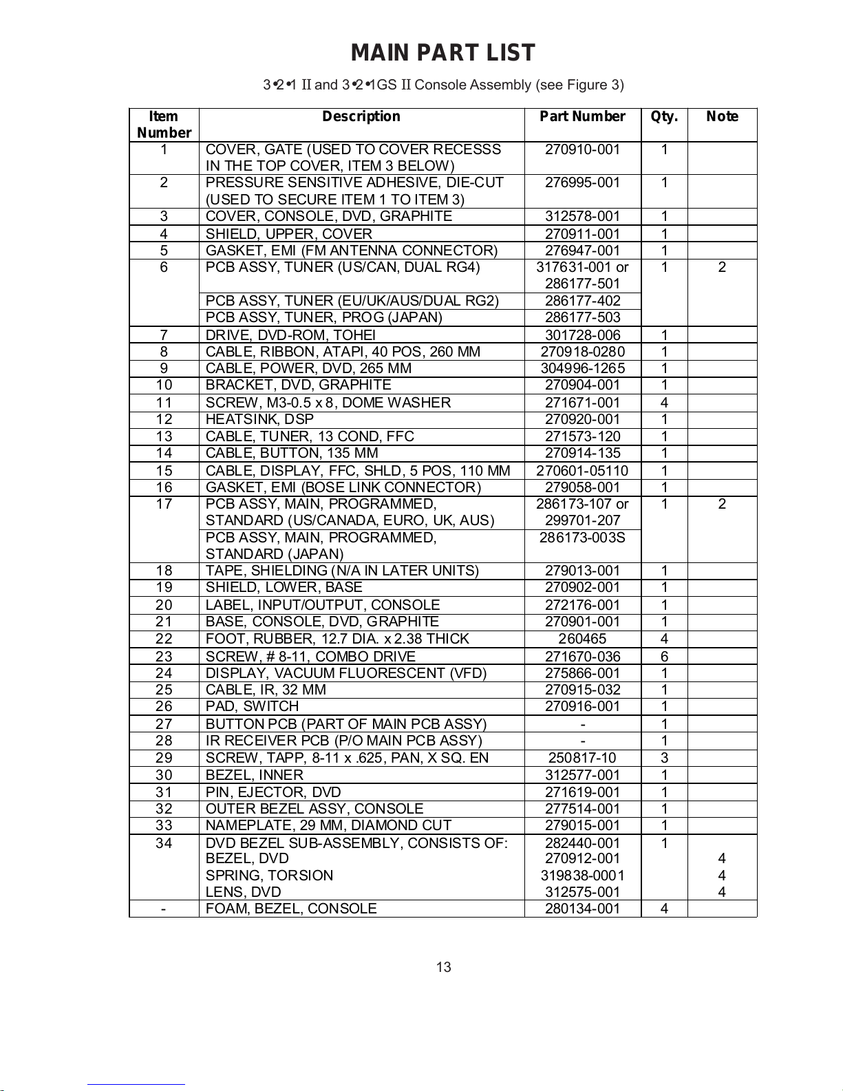
MAIN PART LIST
3•2•1 II and 3•2•1GS II Console Assembly (see Figure 3)
Item
Number
Description Part Number Qty. Note
1 COVER, GATE (USED TO COVER RECESSS
IN THE TOP COVER, ITEM 3 BELOW)
270910-001 1
2 PRESSURE SENSITI VE ADHESIVE, DI E-C UT
(U SED TO SECUR E ITEM 1 TO I TEM 3)
276995-001 1
3 COVER, CONSOLE, DVD, GRAPHITE 312578-001 1
4 SHIELD, UPPER, COVER 270911-001 1
5 GASKET, EMI (FM ANTENNA CONNECTOR) 276947-001 1
6 PCB ASSY, TUNER (US/CAN, DUAL RG4) 317631-001 or
286177-501
1 2
PCB ASSY, TUNER (EU/UK/AUS/DUAL RG2) 286177-402
PCB ASSY, TUNER, PROG (JAPAN) 286177-503
7 DRIVE, DVD-ROM, TOHEI 301728-006 1
8 CABLE, RIBBON, ATAPI, 40 POS, 260 MM 270918-0280 1
9 CABLE, POWER, DVD, 265 MM 304996-1265 1
10 BRACKET, DVD, GRAPHITE 270904-001 1
11 SCREW, M3-0.5 x 8, DOME W ASHER 271671-001 4
12 HEATSINK, DSP 270920-001 1
13 CABLE, TUNER, 13 COND, FFC 271573- 120 1
14 CABLE, BUTTON, 135 MM 270914-135 1
15 CABLE, DISPLAY, FFC, SHLD, 5 POS, 110 MM 270601-05110 1
16 GASKET, EMI (BOSE LINK CONNECTOR) 279058-001 1
17 PCB ASSY, MAIN, PROGRAMMED,
STANDARD (US/CANADA, EURO, UK, AUS)
286173-107 or
299701-207
1 2
PCB ASSY, MAIN, PROGRAMMED,
STANDARD (JAPAN)
286173-003S
18 TAPE, SHIELDING (N/A IN LATER UNITS) 279013-001 1
19 SHIELD, LOWER, BASE 270902-001 1
20 LABEL, INPUT/OUTPUT, CONSOLE 272176-001 1
21 BASE, CONSOLE, DVD, G RAPHITE 270901-001 1
22 FOOT, RUBBER, 12.7 DIA. x 2.38 THICK 260465 4
23 SCREW, # 8-11, COMBO DRIVE 271670-036 6
24 DISPLAY, VACUUM FLUORESCENT (VFD) 275866-001 1
25 CABLE, IR, 32 MM 270915-032 1
26 PAD, SWITCH 270916-001 1
27 BUTTON PCB (PART OF MAIN PCB ASSY) - 1
28 IR RECEIVER PCB (P/O MAIN PCB ASSY) - 1
29 SCREW, TAPP, 8-11 x .625, PAN, X SQ. EN 250817-10 3
30 BEZEL, INNER 312577-001 1
31 PIN, EJECTOR, DVD 271619-001 1
32 OUTER BEZEL ASSY, CONSOLE 277514-001 1
33 NAMEPLATE, 29 MM, DIAMOND CUT 279015-001 1
34 DVD BEZEL SU B- ASSEMBLY, CONS ISTS OF:
BEZEL, DVD
SPRING, TORSION
LENS, DVD
282440-001
270912-001
319838-0001
312575-001
1
4
4
4
- FOAM, BEZEL, CONSOLE 280134-001 4
Page 14
14
Figure 3. 3
•2•1 Series II Standard Console Exploded View
1
2
3
4
5
6
7
8
9
10
11
4x
12
13
16
14
15
17
18
19
20
25
21
22 4x
23 6x
24
27
3x
26
28
29
30
31
32
33
34
Page 15
15
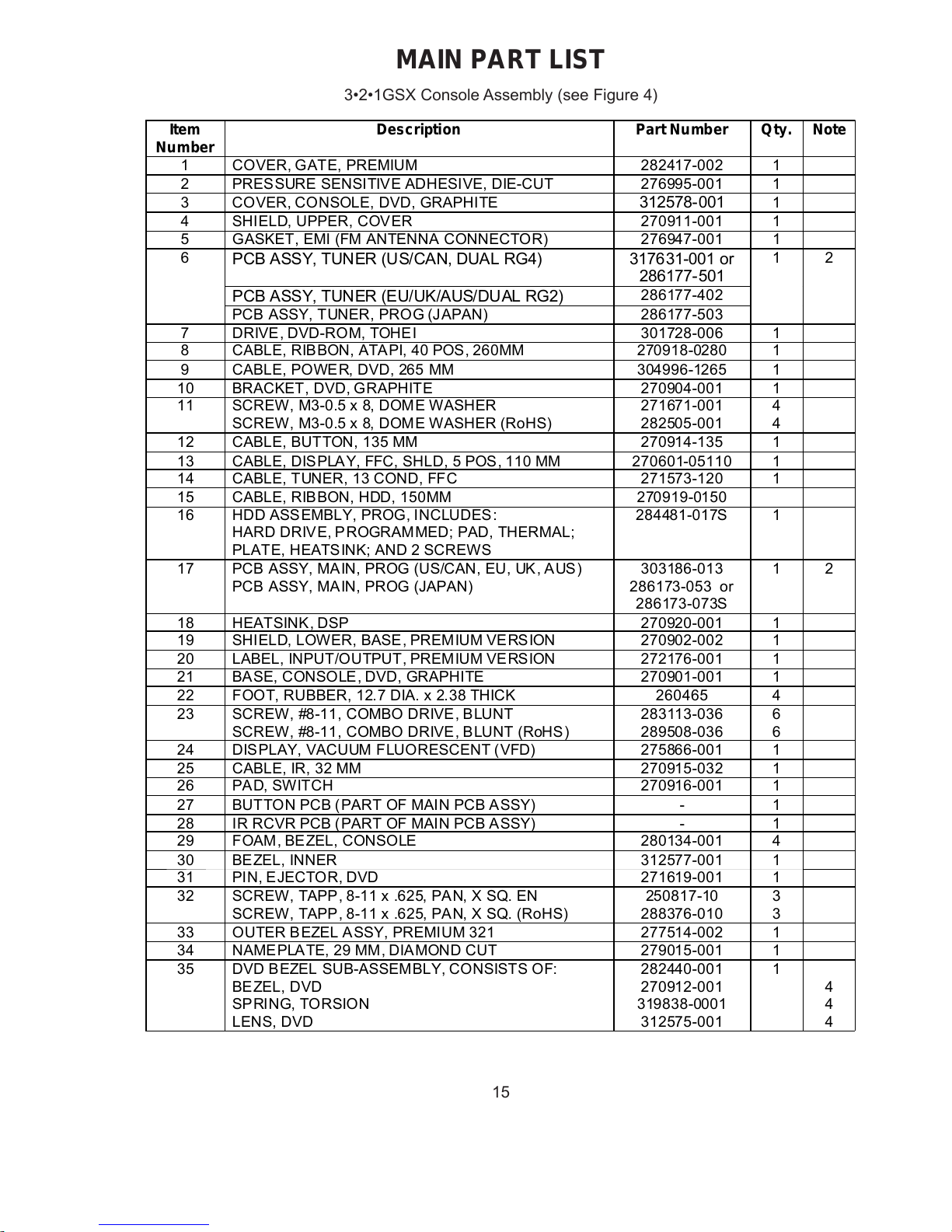
MAIN PART LIST
3•2•1GSX Console Assembly (see Figure 4)
Item
Number
Description Part Number Qty. Note
1 COVER, GATE, PREMIUM 282417-002 1
2 PRESSURE SENSITIVE ADHESIVE, DIE-CUT 276995-001 1
3 COVER, CONSOLE, DVD, GRAPHITE 312578-001 1
4 SHIELD, UPPER, COVER 270911-001 1
5 GASKET, EMI (FM ANTENNA CONNECTOR) 276947-001 1
6
PCB ASSY, TUNER (US/CAN, DUAL RG4) 317631-001 or
286177-501
1 2
PCB ASSY, TUNER (EU/UK/AUS/DUAL RG2)
286177-402
PCB ASSY, TUNER, PROG (JAPAN) 286177-503
7 DRIVE , DVD-ROM, TOHEI 301728-006 1
8 CABLE, RIBBON, ATAPI, 40 POS, 260MM 270918-0280 1
9 CABLE, POWER, DVD, 265 MM 304996-1265 1
10 BRACKET, DVD, GRAPHITE 270904-001 1
11 SCREW, M3-0.5 x 8, DOME WASHER 271671-001 4
SCREW, M3-0.5 x 8, DOME WASHER (RoHS) 282505-001 4
12 CABLE, BUTTON, 135 MM 270914-135 1
13 CABLE, DISPLAY, FFC, SHLD, 5 POS, 110 MM 270601-05110 1
14 CABLE, TUNER, 13 COND, FFC 271573-120 1
15 CABLE, RIBBON, HDD, 150MM 270919-0150
16 HDD ASSEMBLY, PROG, INCLUDES :
HARD DRIVE, PROGRAMMED; PAD, THERMAL;
PLATE, HEATSINK; AND 2 SCREWS
284481-017S 1
17 PCB ASSY, MAIN, PROG (US/CAN, EU, UK , A US) 303186-013 1 2
PCB ASSY, MAIN, PROG (JAPAN) 286173-053 or
286173-073S
18 HEATSINK, DSP 270920-001 1
19 SHIELD, LOWER, BASE , PREMIUM VERS ION 270902-002 1
20 LABEL, INPUT/OUTPUT, PREMIUM VERSION 272176-001 1
21 BASE, CONSOLE, DVD, GRAPHITE 270901-001 1
22 FOOT, RUBBER, 12.7 DIA. x 2.38 THICK 260465 4
23 SCREW, #8-11, COMBO DRIVE, BLUNT 283113-036 6
SCREW, #8-11, COMBO DRIVE, BLUNT (RoHS) 289508-036 6
24 DISPLAY, VACUUM FLUORESCENT (VFD) 275866-001 1
25 CABLE, IR, 32 MM 270915-032 1
26 PAD, SWITCH 270916-001 1
27 BUTTON PCB ( PART OF MAIN PCB ASSY) - 1
28 IR RCVR PCB (PART OF MAIN PCB ASSY) - 1
29 FOAM, BE ZEL, CONSOLE 280134-001 4
30 BEZEL, INNER 312577-001 1
31 PIN, EJECTOR, DVD 271619-001 1
32 SCREW, TAPP, 8-11 x .625, PAN, X SQ. EN 250817-10 3
SCREW, TAPP, 8-11 x .625, PAN, X SQ. (RoHS) 288376-010 3
33 OUTER BEZEL ASSY, PREMIUM 321 277514-002 1
34 NAMEPLATE, 29 MM, DIAMOND CUT 279015-001 1
35 DVD B EZEL SUB-ASSEM BLY, CONSISTS OF:
BEZEL, DVD
SPRING, TORSION
LENS, DVD
282440-001
270912-001
319838-0001
312575-001
1
4
4
4
Page 16
16
Figure 4. 3
•2•1GSX Series II Premium Console Exploded View
1
2
3
4
5
6
7
8
9
10
11
4x
12
13
14
15
16
17
18
19
20
21
22234x
6x
24
25
26
27
28
294x
30
31
32
33
34
35
3x
Page 17
17
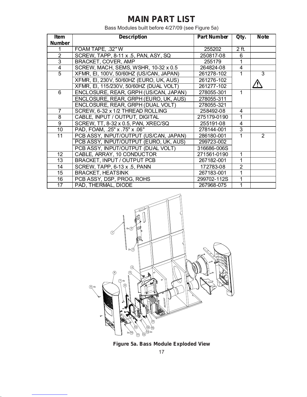
Figure 5a. Bass Module Exploded View
MAIN PART LIST
Bass Modules built before 4/27/09 (see Figure 5a)
1
26x
32x
4
5
6
7
8
94x
4x
103x
11
12
13
14
15
16
17
2x
Item
Number
Description Part Number Qty. Note
1 FOAM TAPE, .32" W 255202 2 ft.
2 SCREW, TAPP, 8-11 x .5, PAN, ASY, SQ 250817-08 6
3 BRACKET, COVER, AMP 255179 1
4 SCREW, MACH, SEMS, WSHR, 10-32 x 0.5 264824-0 8 4
5 XFMR, EI, 100V, 50/60HZ (US/CAN, JAPAN) 261278-102 1 3
XFMR, EI, 230V, 50/60HZ (EURO, UK, AUS) 261276-102
XFMR, EI, 115/230V, 50/60HZ (DUAL VOLT) 261277 -102
6 ENCLOSURE, REAR, GRPH (US/CAN, JAPAN) 278055-301 1
ENCL OSURE, R EAR, GRPH
(
EURO, UK, AUS) 278055-311
ENCLOSURE, REAR, GRPH (DUAL VOLT) 278055-321
7 SCREW, 6- 32 x 1 /2 THREAD ROLLING 25 8492-08 4
8 CABLE, INPUT / OUTPUT, DIGITAL 275 179-0190 1
9 SCREW, TT, 8-32 x 0.5, PAN, XREC/SQ 255191-08 4
10 PAD, FOAM, .25" x .75" x .06" 278144 -001 3
11 PCB ASSY, INPUT/OUTPUT (US/CAN, JAPAN) 286180-001 1 2
PCB ASSY, INPUT/OUTPUT (EURO, UK, AUS) 299723-002
PCB ASSY, IN PUT/OUTPUT (DUAL VOLT) 316686-006S
12 CABLE, ARRAY, 10 CONDUCTOR 271561-0190 1
13 BRACKET, INPUT / OUTPUT PCB 267182-001 1
14 SCREW, TAPP, 6-13 x .5, PANN 172783-08 2
15 BRACKET, HEATSINK 267183-001 1
16 PCB ASSY, DSP, PROG, ROHS 299702-112S 1
17 PAD, THERMAL, DIODE 267968-075 1
Page 18
18
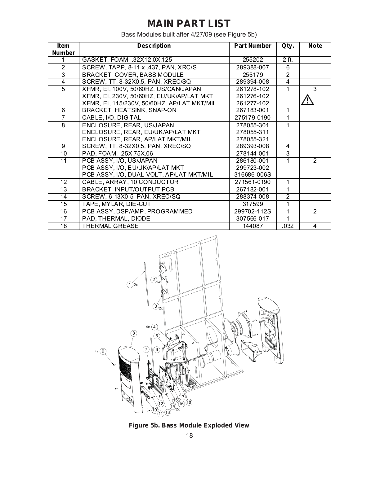
Figure 5b. Bass Module Exploded View
MAIN PART LIST
Bass Modules built after 4/27/09 (see Figure 5b)
18
17
16
15
14
2x
13
12
11
10
3x
9
4x
8
7
6
5
4
4x
3
2x
2
6x
1
2x
Item
Number
Description Part Number Qty. Note
1 GASKET, FOAM, .32X12.0X.125 255202 2 ft.
2 SCREW, TAPP, 8-11 x .437, PAN, XRC/S 289388-007 6
3 BRACKET, COVER, BASS MODULE 255179 2
4 SCREW, TT, 8-32X0.5, PAN, XREC/SQ 289394-008 4
5 XFMR, EI, 100V, 50/60HZ, US/CAN/JAPAN 261278-102 1 3
XFMR, EI, 230V, 50/60HZ, EU/UK/AP/LAT MKT 261276-102
XFMR, EI, 115/230V, 50/60HZ, AP/LAT MKT/MIL 261277-102
6 BRACKET, HEATSINK, SNAP-ON 267183-001 1
7 CABLE, I/O, DIGITAL 275179-0190 1
8 ENCLOSURE, REAR, US/JAPAN 278055-301 1
ENCLOSURE, REAR, EU/UK/AP/LAT MKT 278055-311
ENCLOSURE, REAR, AP/LAT MKT/MIL 278055-321
9 SCREW, TT, 8-32X0.5, PAN, XREC/SQ 289393-008 4
10 PAD, FOAM, .25X.75X.06 278144-001 3
11 PCB ASSY, I/O, US/JAPAN 286180-001 1 2
PCB ASSY, I/O, E U/UK/AP/LAT MKT 299723-002
PCB ASSY, I/O, DUAL VOLT, A P/LAT MKT/MIL 316686-006S
12 CABLE, ARRAY, 10 CONDUCTOR 271561-0190 1
13 BRACKET, INPUT/OUTPUT PCB 267182-001 1
14 S CREW, 6-13X0.5, PAN, XREC/SQ 288374-008 2
15 TAPE, MYLAR, DIE-CUT 317599 1
16 PCB ASSY, DSP/AMP, PROGRAMMED 299702-112S 1 2
17 P AD, THERMAL, DIODE 307566-017 1
18 THERMAL GREASE 144087 .032 4
Page 19
19
MAIN PART LIST
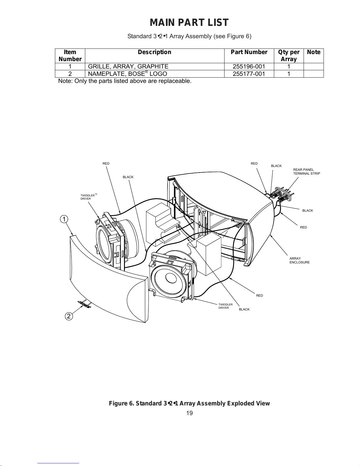
Standard 3•2•1 Array Assembly (see Figure 6)
Figure 6. Standard 3
•2•1 Array Assembly Exploded View
RED
BLACK
RED
BLACK
1
2
TWIDDLER
DRIVER
TWIDDLER
DRIVER
TM
ARRAY
ENCLOSURE
RED
BLACK
RED
BLACK
REAR PANEL
TERMINAL STRIP
Item
Number
Description Part Number Qty per
Array
Note
1 GRILLE, ARRAY, GRAPHITE 255196-001 1
2 NAMEPLATE, BOSE® LOGO 255177-001 1
Note: Only the parts listed above are replaceable.
Page 20
20
MAIN PART LIST
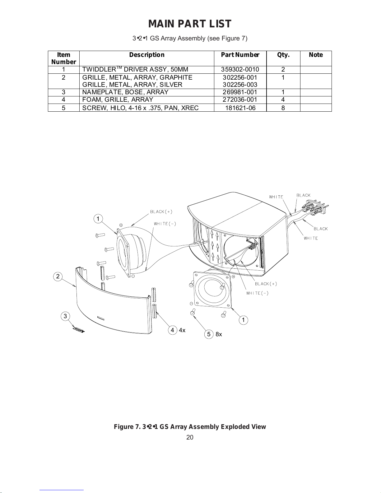
3•2•1 GS Array Assembly (see Figure 7)
1
2
3
44x
58x
1
Figure 7. 3•2•1 GS Array Assembly Exploded View
Item
Numb er
Description Part Number Qty. Note
1 TWIDDLERTM DRIVER ASSY, 50MM 359302-0010 2
2 GRILLE, METAL, ARRAY, GRAPHITE
GRILLE , METAL, ARRAY, SILVER
302256-001
302256-003
1
3 NAMEPLATE, BOSE, ARRAY 2 69981-001 1
4 FOAM, GRILLE, ARRAY 272036-001 4
5 SCREW, HILO, 4-16 x .375, P AN, XREC 181621-06 8
Page 21
21
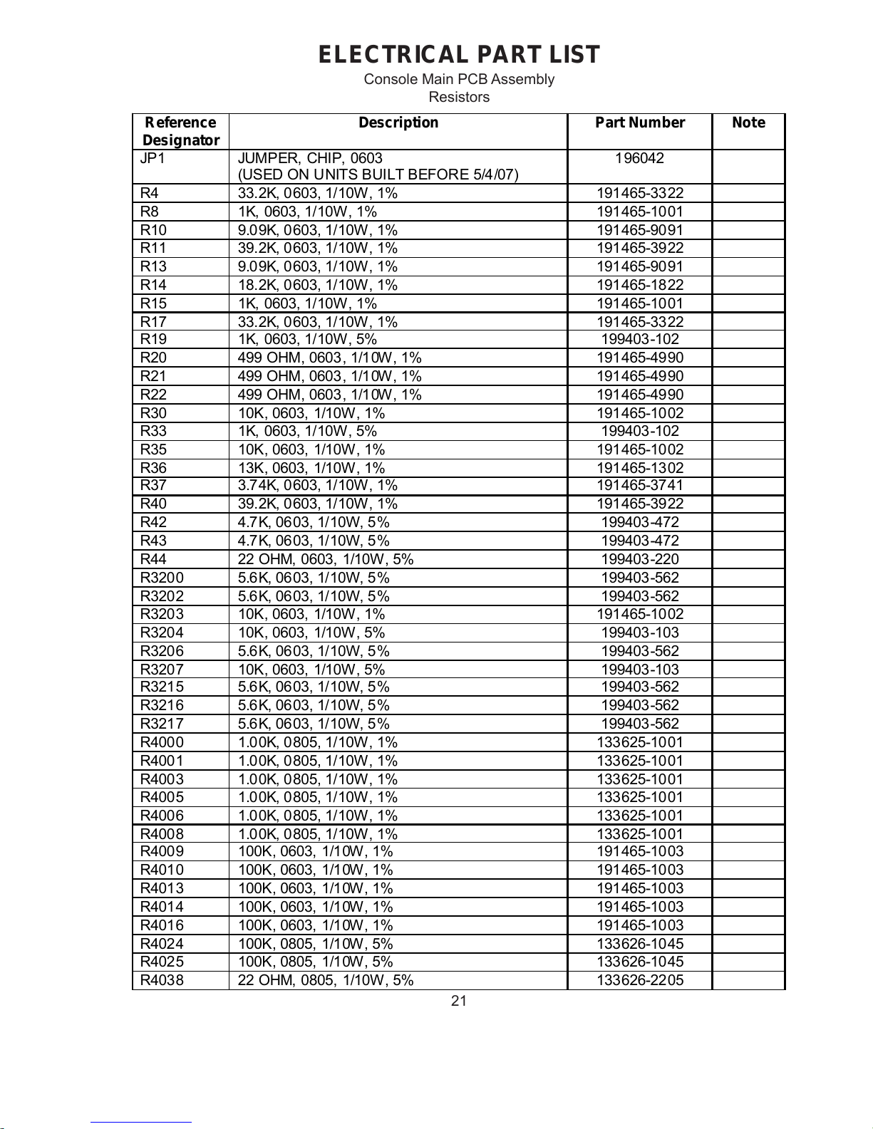
ELECTRICAL PART LIST
Resistors
Console Main PCB Assembly
Reference
Designator
Description Part Number Note
JP1 JUMPER, CHIP, 0603
(USED ON UNITS BUILT BEFORE 5/4/07)
196042
R4 33.2K, 0603, 1/10W, 1% 191 465-3322
R8 1K, 0603, 1/10W , 1% 191 465-1001
R10 9.09K, 0603, 1/10W, 1% 191465-9091
R11 39.2K, 0603, 1/10W, 1% 191465-3922
R13 9.09K, 0603, 1/10W, 1% 191465-9091
R14 18.2K, 0603, 1/10W, 1% 191465-1822
R15 1K, 0603, 1/10W , 1% 191465-1001
R17 33.2K, 0603, 1/10W, 1% 191465-3322
R19 1K, 0603, 1/10W , 5% 199403-102
R20 499 OHM, 0603, 1/10W, 1% 191465-4990
R21 499 OHM, 0603, 1/10W, 1% 191465-4990
R22 499 OHM, 0603, 1/10W, 1% 191465-4990
R30 10K, 0603, 1/10W, 1% 191465-1002
R33 1K, 0603, 1/10W , 5% 199403-102
R35 10K, 0603, 1/10W, 1% 191465-1002
R36 13K, 0603, 1/10W, 1% 191465-1302
R37 3.74K, 0603, 1/10W, 1% 191465-3741
R40 39.2K, 0603, 1/10W, 1% 191465-3922
R42 4.7K, 06 03, 1/10W, 5% 199403 -472
R43 4.7K, 06 03, 1/10W, 5% 199403 -472
R44 22 OHM, 0603, 1/10W, 5% 199403-220
R3200 5.6K, 06 03, 1/10W, 5 % 199403 -562
R3202 5.6K, 06 03, 1/10W, 5 % 199403 -562
R3203 10K, 0603, 1/10W , 1% 191465-10 02
R3204 10K, 0603, 1/10W , 5% 199403-103
R3206 5.6K, 06 03, 1/10W, 5 % 199403 -562
R3207 10K, 0603, 1/10W , 5% 199403-103
R3215 5.6K, 06 03, 1/10W, 5 % 199403 -562
R3216 5.6K, 06 03, 1/10W, 5 % 199403 -562
R3217 5.6K, 06 03, 1/10W, 5 % 199403 -562
R4000 1.0 0K, 0805, 1/10W, 1% 133625-1001
R4001 1.0 0K, 0805, 1/10W, 1% 133625-1001
R4003 1.0 0K, 0805, 1/10W, 1% 133625-1001
R4005 1.0 0K, 0805, 1/10W, 1% 133625-1001
R4006 1.0 0K, 0805, 1/10W, 1% 133625-1001
R4008 1.0 0K, 0805, 1/10W, 1% 133625-1001
R4009 100K, 0603, 1/1 0W, 1% 191 465-1003
R4010 100K, 0603, 1/1 0W, 1% 191 465-1003
R4013 100K, 0603, 1/1 0W, 1% 191 465-1003
R4014 100K, 0603, 1/1 0W, 1% 191 465-1003
R4016 100K, 0603, 1/1 0W, 1% 191 465-1003
R4024 100K, 0805, 1/1 0W, 5% 133 626-1045
R4025 100K, 0805, 1/1 0W, 5% 133 626-1045
R4038 22 OHM, 0805, 1/10W, 5% 133626-2205
Page 22
22
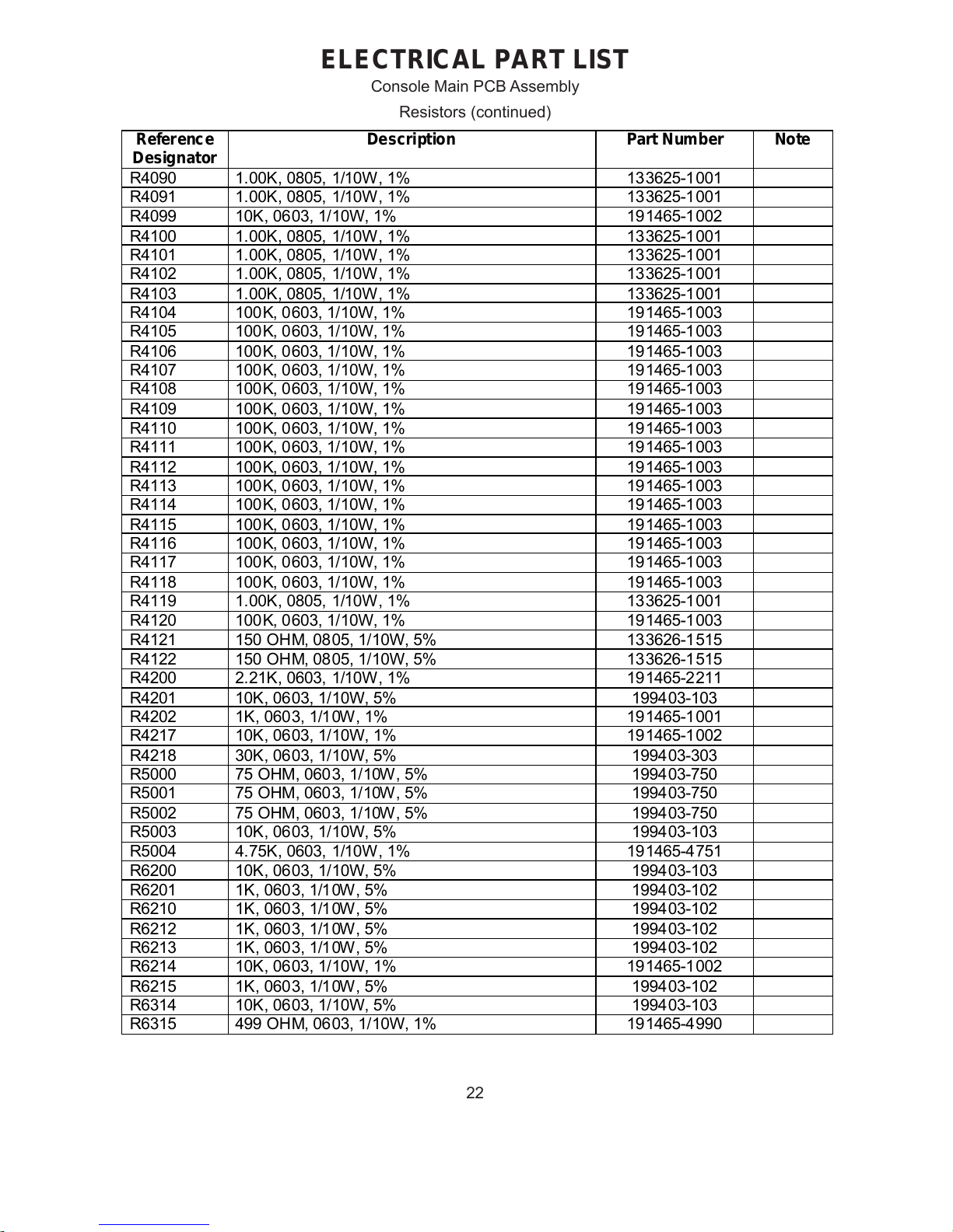
ELECTRICAL PART LIST
Resistors (continued)
Console Main PCB Assembly
Reference
Designator
Description Part Number Note
R4090 1.00K, 0805, 1/10W, 1% 133625-1001
R4091 1.00K, 0805, 1/10W, 1% 133625-1001
R4099 10K, 0603, 1/10W, 1% 191465-1002
R4100 1.00K, 0805, 1/10W, 1% 133625-1001
R4101 1.00K, 0805, 1/10W, 1% 133625-1001
R4102 1.00K, 0805, 1/10W, 1% 133625-1001
R4103 1.00K, 0805, 1/10W, 1% 133625-1001
R4104 100K, 0603, 1/10W, 1% 19 1465-1003
R4105 100K, 0603, 1/10W, 1% 19 1465-1003
R4106 100K, 0603, 1/10W, 1% 19 1465-1003
R4107 100K, 0603, 1/10W, 1% 19 1465-1003
R4108 100K, 0603, 1/10W, 1% 19 1465-1003
R4109 100K, 0603, 1/10W, 1% 19 1465-1003
R4110 100K, 0603, 1/10W, 1% 19 1465-1003
R4111 100K, 0603, 1/10W, 1% 19 1465-1003
R4112 100K, 0603, 1/10W, 1% 19 1465-1003
R4113 100K, 0603, 1/10W, 1% 19 1465-1003
R4114 100K, 0603, 1/10W, 1% 19 1465-1003
R4115 100K, 0603, 1/10W, 1% 19 1465-1003
R4116 100K, 0603, 1/10W, 1% 19 1465-1003
R4117 100K, 0603, 1/10W, 1% 19 1465-1003
R4118 100K, 0603, 1/10W, 1% 19 1465-1003
R4119 1.00K, 0805, 1/10W, 1% 133625-1001
R4120 100K, 0603, 1/10W, 1% 19 1465-1003
R4121 150 OHM, 08 05, 1/10W, 5% 133626-1515
R4122 150 OHM, 08 05, 1/10W, 5% 133626-1515
R4200 2.21K, 0603, 1/10W, 1% 191465-2211
R4201 10K, 0603, 1/10W, 5% 199403-103
R4202 1K, 060 3, 1/10W, 1% 191465-1001
R4217 10K, 0603, 1/10W, 1% 191465-1002
R4218 30K, 0603, 1/10W, 5% 199403-303
R5000 75 OHM, 060 3, 1/10W, 5% 199403-750
R5001 75 OHM, 060 3, 1/10W, 5% 199403-750
R5002 75 OHM, 060 3, 1/10W, 5% 199403-750
R5003 10K, 0603, 1/10W, 5% 199403-103
R5004 4.75K, 0603, 1/10W, 1% 191465-4751
R6200 10K, 0603, 1/10W, 5% 199403-103
R6201 1K, 060 3, 1/10W, 5% 199403-102
R6210 1K, 060 3, 1/10W, 5% 199403-102
R6212 1K, 060 3, 1/10W, 5% 199403-102
R6213 1K, 060 3, 1/10W, 5% 199403-102
R6214 10K, 0603, 1/10W, 1% 191465-1002
R6215 1K, 060 3, 1/10W, 5% 199403-102
R6314 10K, 0603, 1/10W, 5% 199403-103
R6315 499 OHM, 06 03, 1/10W, 1% 191465-4990
Page 23
23
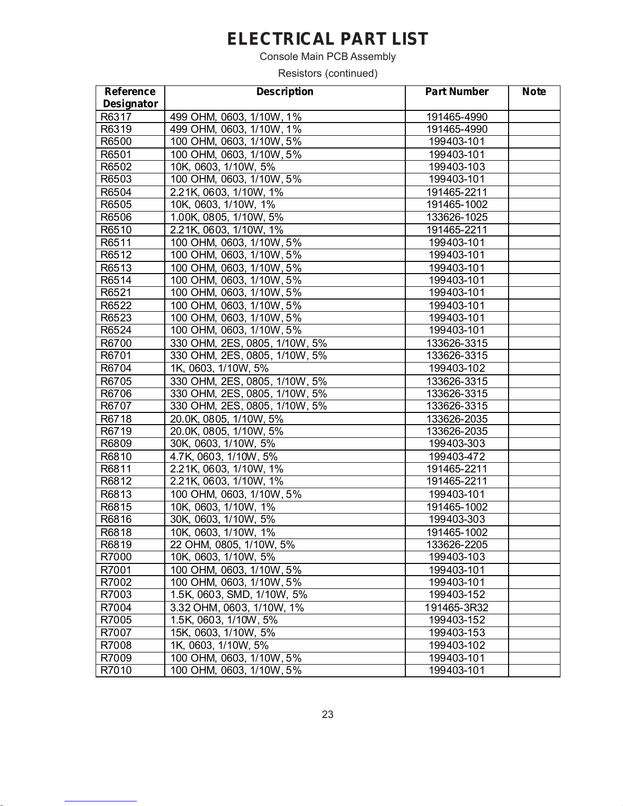
ELECTRICAL PART LIST
Console Main PCB Assembly
Resistors (continued)
Reference
Designator
Description Part Number Note
R6317 499 OHM, 0603, 1/10W , 1% 191465-4990
R6319 499 OHM, 0603, 1/10W , 1% 191465-4990
R6500 100 OHM, 0603, 1/10W , 5% 199403-10 1
R6501 100 OHM, 0603, 1/10W , 5% 199403-10 1
R6502 10K, 0603, 1/10W, 5% 199403-103
R6503 100 OHM, 0603, 1/10W , 5% 199403-10 1
R6504 2.21K, 06 03, 1/10W, 1% 191465-2211
R6505 10K, 0603, 1/10W, 1% 191465-1002
R6506 1.00K, 08 05, 1/10W, 5% 133626-1025
R6510 2.21K, 06 03, 1/10W, 1% 191465-2211
R6511 100 OHM, 0603, 1/10W , 5% 199403-10 1
R6512 100 OHM, 0603, 1/10W , 5% 199403-10 1
R6513 100 OHM, 0603, 1/10W , 5% 199403-10 1
R6514 100 OHM, 0603, 1/10W , 5% 199403-10 1
R6521 100 OHM, 0603, 1/10W , 5% 199403-10 1
R6522 100 OHM, 0603, 1/10W , 5% 199403-10 1
R6523 100 OHM, 0603, 1/10W , 5% 199403-10 1
R6524 100 OHM, 0603, 1/10W , 5% 199403-10 1
R6700 330 OHM, 2ES, 0805, 1/10W, 5% 133626-3315
R6701 330 OHM, 2ES, 0805, 1/10W, 5% 133626-3315
R6704 1K, 0603, 1/10W, 5% 199403-10 2
R6705 330 OHM, 2ES, 0805, 1/10W, 5% 133626-3315
R6706 330 OHM, 2ES, 0805, 1/10W, 5% 133626-3315
R6707 330 OHM, 2ES, 0805, 1/10W, 5% 133626-3315
R6718 20.0K, 08 05, 1/10W, 5% 133626-2035
R6719 20.0K, 08 05, 1/10W, 5% 133626-2035
R6809 30K, 0603, 1/10W, 5% 199403-303
R6810 4.7K, 060 3, 1/10W , 5% 199403-472
R6811 2.21K, 06 03, 1/10W, 1% 191465-2211
R6812 2.21K, 06 03, 1/10W, 1% 191465-2211
R6813 100 OHM, 0603, 1/10W , 5% 199403-10 1
R6815 10K, 0603, 1/10W, 1% 191465-1002
R6816 30K, 0603, 1/10W, 5% 199403-303
R6818 10K, 0603, 1/10W, 1% 191465-1002
R6819 22 OHM, 0805, 1/10W, 5% 133626- 2205
R7000 10K, 0603, 1/10W, 5% 199403-103
R7001 100 OHM, 0603, 1/10W , 5% 199403-10 1
R7002 100 OHM, 0603, 1/10W , 5% 199403-10 1
R7003 1.5K, 060 3, SMD, 1/10W, 5% 199403-15 2
R7004 3.32 OHM, 0603, 1/10W, 1% 1 91465-3R32
R7005 1.5K, 060 3, 1/10W , 5% 199403-152
R7007 15K, 0603, 1/10W, 5% 199403-153
R7008 1K, 0603, 1/10W, 5% 199403-10 2
R7009 100 OHM, 0603, 1/10W , 5% 199403-10 1
R7010 100 OHM, 0603, 1/10W , 5% 199403-10 1
Page 24
24
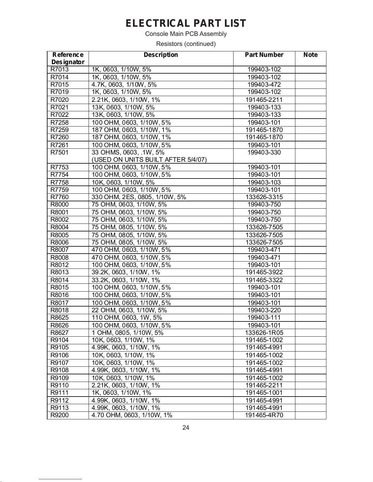
ELECTRICAL PART LIST
Console Main PCB Assembly
Resistors (continued)
Reference
Designator
Description Part Number Note
R7013 1K, 0603, 1/10W, 5% 199403-102
R7014 1K, 0603, 1/10W, 5% 199403-102
R7015 4.7K, 0603, 1/10W, 5% 199403-472
R7019 1K, 0603, 1/10W, 5% 199403-102
R7020 2.21K, 0603 , 1/10W , 1% 191465-2211
R7021 13K, 0603, 1/10W, 5% 199403-133
R7022 13K, 0603, 1/10W, 5% 199403-133
R7258 100 OHM, 0 603, 1/10W, 5% 199403-101
R7259 187 OHM, 0 603, 1/10W, 1% 191 465-1870
R7260 187 OHM, 0 603, 1/10W, 1% 191 465-1870
R7261 100 OHM, 0 603, 1/10W, 5% 199403-101
R7501 33 OHMS, 0603, .1W, 5%
(
USED ON UNITS BUILT AFTER 5/4/07)
199403-330
R7753 100 OHM, 0 603, 1/10W, 5% 199403-101
R7754 100 OHM, 0 603, 1/10W, 5% 199403-101
R7758 10K, 0603, 1/10W, 5% 199403-103
R7759 100 OHM, 0 603, 1/10W, 5% 199403-101
R7760 33 0 OHM, 2 ES, 0805, 1/10W, 5% 133626-3315
R8000 75 OHM, 06 03, 1/10W, 5% 199403-750
R8001 75 OHM, 06 03, 1/10W, 5% 199403-750
R8002 75 OHM, 06 03, 1/10W, 5% 199403-750
R8004 75 OHM, 08 05, 1/10W, 5% 133626-7505
R8005 75 OHM, 08 05, 1/10W, 5% 133626-7505
R8006 75 OHM, 08 05, 1/10W, 5% 133626-7505
R8007 470 OHM, 0 603, 1/10W, 5% 199403-471
R8008 470 OHM, 0 603, 1/10W, 5% 199403-471
R8012 100 OHM, 0 603, 1/10W, 5% 199403-101
R8013 39.2K, 0603 , 1/10W , 1% 191465-3922
R8014 33.2K, 0603 , 1/10W , 1% 191465-3322
R8015 100 OHM, 0 603, 1/10W, 5% 199403-101
R8016 100 OHM, 0 603, 1/10W, 5% 199403-101
R8017 100 OHM, 0 603, 1/10W, 5% 199403-101
R8018 22 OHM, 06 03, 1/10W, 5% 199403-220
R8625 110 OHM, 0 603, 1W, 5% 199403-111
R8626 100 OHM, 0 603, 1/10W, 5% 199403-101
R8627 1 OHM, 080 5, 1/10W, 5% 133626-1R05
R9104 10K, 0603, 1/10W, 1% 191 465-1002
R9105 4.99K, 0603 , 1/10W , 1% 191465-4991
R9106 10K, 0603, 1/10W, 1% 191 465-1002
R9107 10K, 0603, 1/10W, 1% 191 465-1002
R9108 4.99K, 0603 , 1/10W , 1% 191465-4991
R9109 10K, 0603, 1/10W, 1% 191 465-1002
R9110 2.21K, 0603 , 1/10W , 1% 191465-2211
R9111 1K, 0603, 1/10W, 1% 191 465-1001
R9112 4.99K, 0603 , 1/10W , 1% 191465-4991
R9113 4.99K, 0603 , 1/10W , 1% 191465-4991
R9200 4.70 OHM, 0603, 1/10W, 1% 191465-4R70
Page 25
25
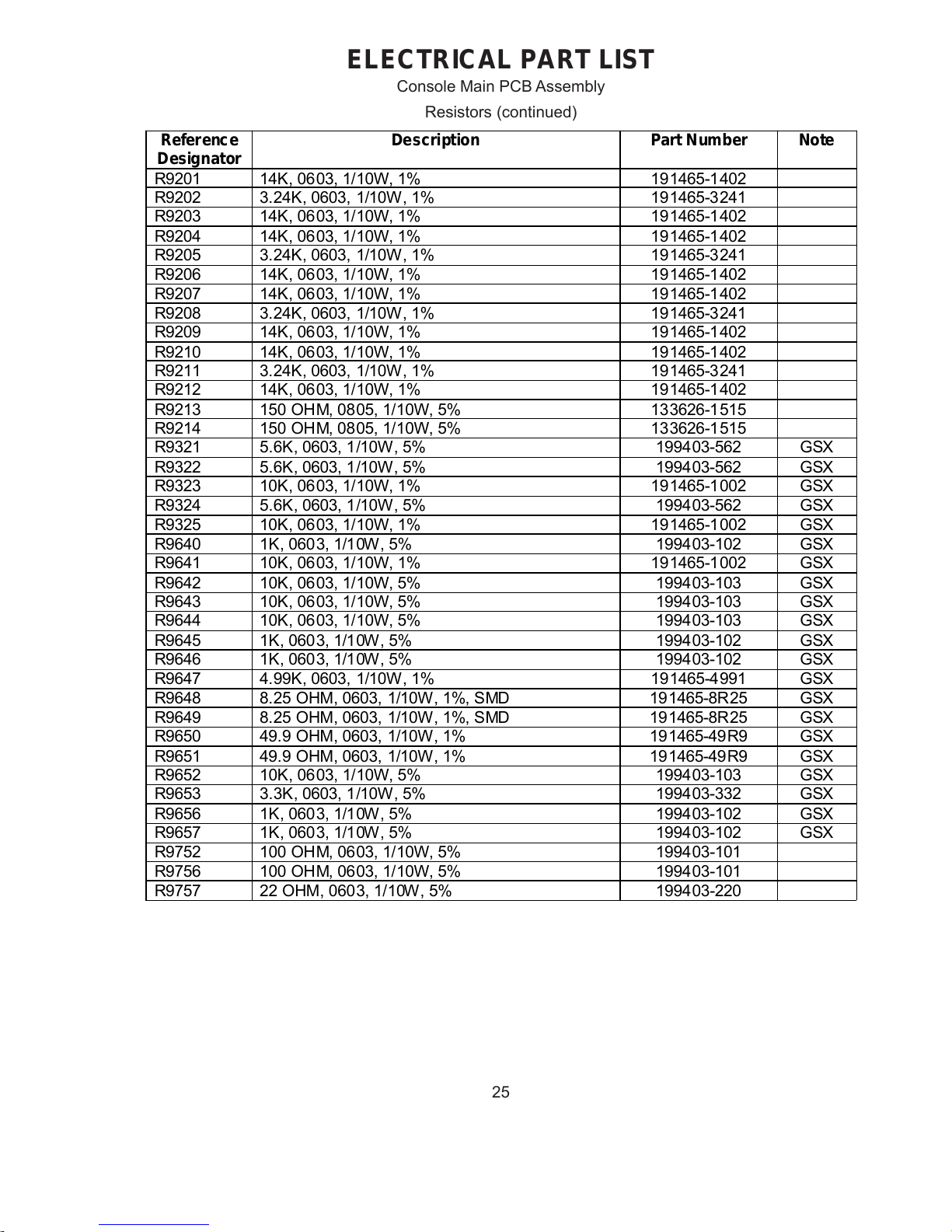
ELECTRICAL PART LIST
Console Main PCB Assembly
Resistors (continued)
Reference
Designator
Description Part Number Note
R9201 14K, 0603, 1/10W, 1% 191465-1402
R9202 3.24K, 0603, 1/10W, 1% 191465-3241
R9203 14K, 0603, 1/10W, 1% 191465-1402
R9204 14K, 0603, 1/10W, 1% 191465-1402
R9205 3.24K, 0603, 1/10W, 1% 191465-3241
R9206 14K, 0603, 1/10W, 1% 191465-1402
R9207 14K, 0603, 1/10W, 1% 191465-1402
R9208 3.24K, 0603, 1/10W, 1% 191465-3241
R9209 14K, 0603, 1/10W, 1% 191465-1402
R9210 14K, 0603, 1/10W, 1% 191465-1402
R9211 3.24K, 0603, 1/10W, 1% 191465-3241
R9212 14K, 0603, 1/10W, 1% 191465-1402
R9213 150 OHM, 08 05, 1/10W, 5% 133626-1515
R9214 150 OHM, 08 05, 1/10W, 5% 133626-1515
R9321 5.6K, 0603, 1/10W, 5% 199403-562 GSX
R9322 5.6K, 0603, 1/10W, 5% 199403-562 GSX
R9323 10K, 0603, 1/10W, 1% 191465-1002 GSX
R9324 5.6K, 0603, 1/10W, 5% 199403-562 GSX
R9325 10K, 0603, 1/10W, 1% 191465-1002 GSX
R9640 1K, 060 3, 1/10W, 5% 199403-102 GSX
R9641 10K, 0603, 1/10W, 1% 191465-1002 GSX
R9642 10K, 0603, 1/10W, 5% 199403-103 GSX
R9643 10K, 0603, 1/10W, 5% 199403-103 GSX
R9644 10K, 0603, 1/10W, 5% 199403-103 GSX
R9645 1K, 060 3, 1/10W, 5% 199403-102 GSX
R9646 1K, 060 3, 1/10W, 5% 199403-102 GSX
R9647 4.99K, 0603, 1/10W, 1% 191465-4991 GSX
R9648 8.25 OHM, 0603, 1/10W, 1%, SMD 19 1465-8R25 GSX
R9649 8.25 OHM, 0603, 1/10W, 1%, SMD 19 1465-8R25 GSX
R9650 49.9 OHM, 0603, 1/10W, 1% 191465-49R9 GSX
R9651 49.9 OHM, 0603, 1/10W, 1% 191465-49R9 GSX
R9652 10K, 0603, 1/10W, 5% 199403-103 GSX
R9653 3.3K, 0603, 1/10W, 5% 199403-332 GSX
R9656 1K, 060 3, 1/10W, 5% 199403-102 GSX
R9657 1K, 060 3, 1/10W, 5% 199403-102 GSX
R9752 100 OHM, 06 03, 1/10W, 5% 1994 03-101
R9756 100 OHM, 06 03, 1/10W, 5% 1994 03-101
R9757 22 OHM, 060 3, 1/10W, 5% 199403-220
Page 26
26
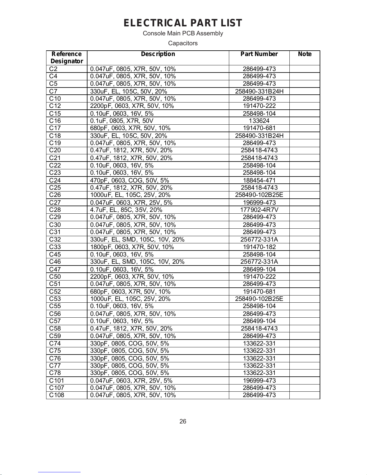
ELECTRICAL PART LIST
Console Main PCB Assembly
Capacitors
Reference
Designator
Description Part Number Note
C2 0.047uF, 0805, X7R, 50V, 10% 286499-473
C4 0.047uF, 0805, X7R, 50V, 10% 286499-473
C5 0.047uF, 0805, X7R, 50V, 10% 286499-473
C7 330uF, EL, 105C, 50V, 20% 258490-331B24H
C10 0.047uF, 0805, X7R, 50V, 10% 286499-473
C12 2200pF, 0603, X7R, 50V, 10% 191470-222
C15 0.10uF, 0603, 16V, 5% 258498- 104
C16 0.1uF, 0805, X7R, 50V 133624
C17 680pF, 0603, X7R, 50V, 10% 191470-681
C18 330uF, EL, 105C, 50V, 20% 258490-331B24H
C19 0.047uF, 0805, X7R, 50V, 10% 286499-473
C20 0.47uF, 1812, X7R, 50V, 20% 258418-4743
C21 0.47uF, 1812, X7R, 50V, 20% 258418-4743
C22 0.10uF, 0603, 16V, 5% 258498- 104
C23 0.10uF, 0603, 16V, 5% 258498- 104
C24 470pF, 0603, COG, 50V, 5% 188454-471
C25 0.47uF, 1812, X7R, 50V, 20% 258418-4743
C26 1000uF, EL, 105C, 25V, 20% 258490-102B25E
C27 0.047uF, 0603, X7R, 25V, 5% 196999-473
C28 4.7uF, EL, 85C, 3 5V, 20% 177 902-4R7V
C29 0.047uF, 0805, X7R, 50V, 10% 286499-473
C30 0.047uF, 0805, X7R, 50V, 10% 286499-473
C31 0.047uF, 0805, X7R, 50V, 10% 286499-473
C32 330uF, EL, SMD, 105C, 10V, 20% 256772-331A
C33 1800pF, 0603, X7R, 50V, 10% 191470-182
C45 0.10uF, 0603, 16V, 5% 258498- 104
C46 330uF, EL, SMD, 105C, 10V, 20% 256772-331A
C47 0.10uF, 0603, 16V, 5% 286499- 104
C50 2200pF, 0603, X7R, 50V, 10% 191470-222
C51 0.047uF, 0805, X7R, 50V, 10% 286499-473
C52 680pF, 0603, X7R, 50V, 10% 191470-681
C53 1000uF, EL, 105C, 25V, 20% 258490-102B25E
C55 0.10uF, 0603, 16V, 5% 258498- 104
C56 0.047uF, 0805, X7R, 50V, 10% 286499-473
C57 0.10uF, 0603, 16V, 5% 286499- 104
C58 0.47uF, 1812, X7R, 50V, 20% 258418-4743
C59 0.047uF, 0805, X7R, 50V, 10% 286499-473
C74 330pF, 0805, COG, 50V, 5% 133622-331
C75 330pF, 0805, COG, 50V, 5% 133622-331
C76 330pF, 0805, COG, 50V, 5% 133622-331
C77 330pF, 0805, COG, 50V, 5% 133622-331
C78 330pF, 0805, COG, 50V, 5% 133622-331
C101 0.047uF, 0603, X7R, 25V, 5% 196999- 473
C107 0.047uF, 0805, X7R, 50V, 10% 286499- 473
C108 0.047uF, 0805, X7R, 50V, 10% 286499-473
Page 27
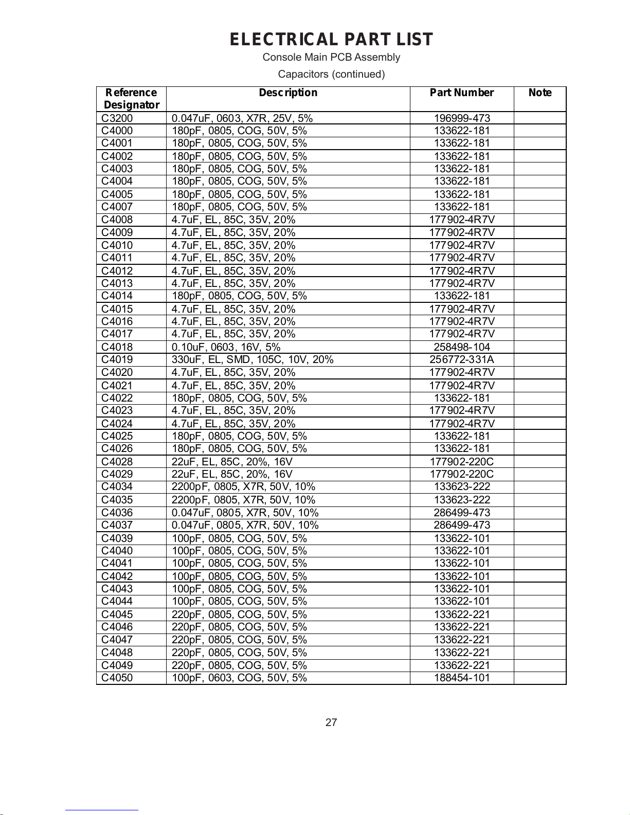
27
ELECTRICAL PART LIST
Capacitors (continued)
Console Main PCB Assembly
Reference
Designator
Description Part Number Note
C3200 0.047uF, 0603, X7R, 25V, 5% 196999-473
C4000 180pF, 0805, COG, 50V, 5% 133622-181
C4001 180pF, 0805, COG, 50V, 5% 133622-181
C4002 180pF, 0805, COG, 50V, 5% 133622-181
C4003 180pF, 0805, COG, 50V, 5% 133622-181
C4004 180pF, 0805, COG, 50V, 5% 133622-181
C4005 180pF, 0805, COG, 50V, 5% 133622-181
C4007 180pF, 0805, COG, 50V, 5% 133622-181
C4008 4.7uF, EL, 85C, 3 5V, 2 0% 177902-4R7V
C4009 4.7uF, EL, 85C, 3 5V, 2 0% 177902-4R7V
C4010 4.7uF, EL, 85C, 3 5V, 2 0% 177902-4R7V
C4011 4.7uF, EL, 85C, 3 5V, 2 0% 177902-4R7V
C4012 4.7uF, EL, 85C, 3 5V, 2 0% 177902-4R7V
C4013 4.7uF, EL, 85C, 3 5V, 2 0% 177902-4R7V
C4014 180pF, 0805, COG, 50V, 5% 133622-181
C4015 4.7uF, EL, 85C, 3 5V, 2 0% 177902-4R7V
C4016 4.7uF, EL, 85C, 3 5V, 2 0% 177902-4R7V
C4017 4.7uF, EL, 85C, 3 5V, 2 0% 177902-4R7V
C4018 0.10uF, 0603, 16V, 5% 258498- 104
C4019 330uF, EL, SMD, 105C, 10V, 20% 256772-331A
C4020 4.7uF, EL, 85C, 3 5V, 2 0% 177902-4R7V
C4021 4.7uF, EL, 85C, 3 5V, 2 0% 177902-4R7V
C4022 180pF, 0805, COG, 50V, 5% 133622-181
C4023 4.7uF, EL, 85C, 3 5V, 2 0% 177902-4R7V
C4024 4.7uF, EL, 85C, 3 5V, 2 0% 177902-4R7V
C4025 180pF, 0805, COG, 50V, 5% 133622-181
C4026 180pF, 0805, COG, 50V, 5% 133622-181
C4028 22uF, EL, 85C , 20%, 16V 177902-220C
C4029 22uF, EL, 85C , 20%, 16V 177902-220C
C4034 2200pF, 0805, X7R, 50V, 10% 133623-222
C4035 2200pF, 0805, X7R, 50V, 10% 133623-222
C4036 0.047uF, 0805, X7R, 50V, 10% 286499-473
C4037 0.047uF, 0805, X7R, 50V, 10% 286499-473
C4039 100pF, 0805, COG, 50V, 5% 133622-101
C4040 100pF, 0805, COG, 50V, 5% 133622-101
C4041 100pF, 0805, COG, 50V, 5% 133622-101
C4042 100pF, 0805, COG, 50V, 5% 133622-101
C4043 100pF, 0805, COG, 50V, 5% 133622-101
C4044 100pF, 0805, COG, 50V, 5% 133622-101
C4045 220pF, 0805, COG, 50V, 5% 133622-221
C4046 220pF, 0805, COG, 50V, 5% 133622-221
C4047 220pF, 0805, COG, 50V, 5% 133622-221
C4048 220pF, 0805, COG, 50V, 5% 133622-221
C4049 220pF, 0805, COG, 50V, 5% 133622-221
C4050 100pF, 0603, COG, 50V, 5% 188454-101
Page 28
28
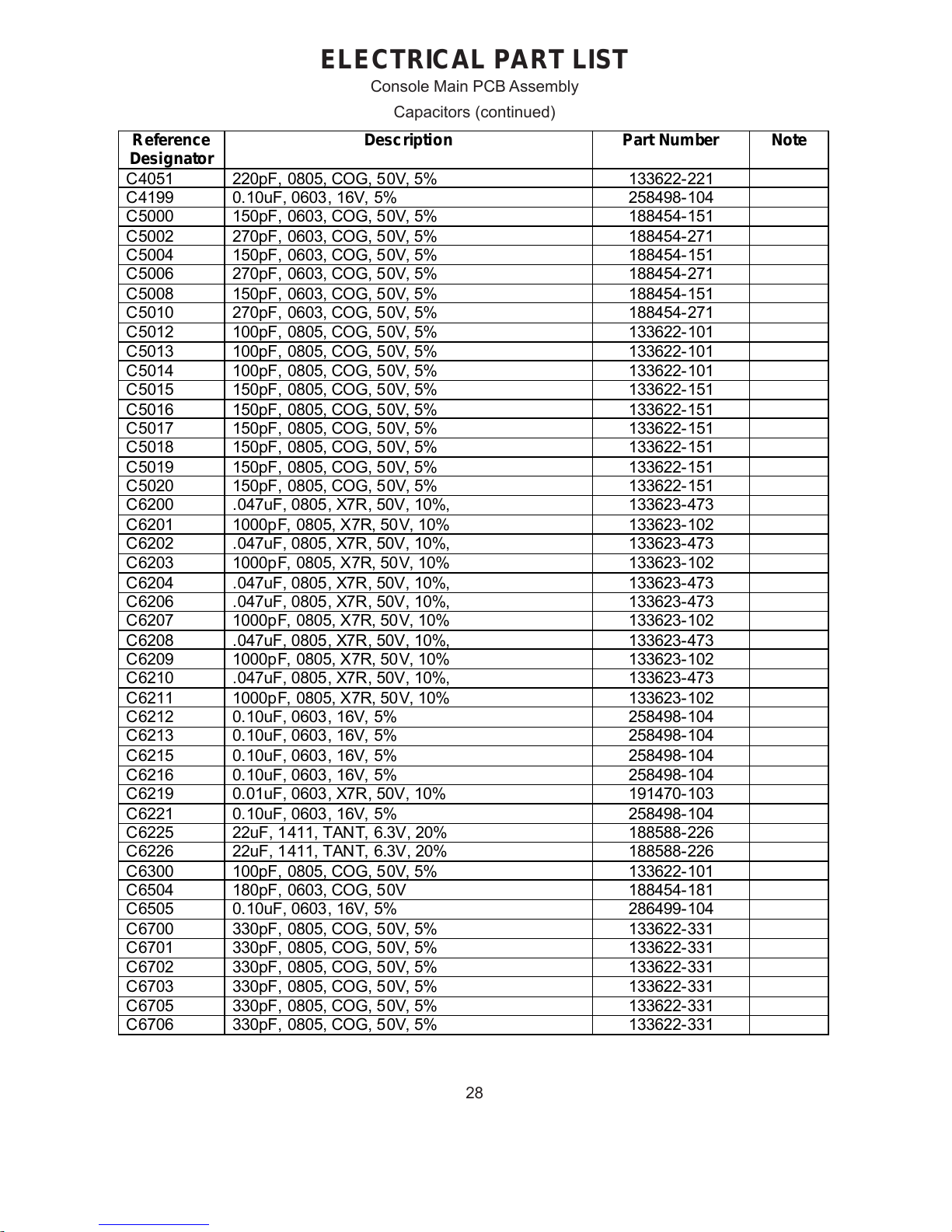
ELECTRICAL PART LIST
Capacitors (continued)
Console Main PCB Assembly
Reference
Designator
Description Part Number Note
C4051 220pF, 0805, COG, 50V, 5% 133622-221
C4199 0.10uF, 0603, 16V, 5% 258498- 104
C5000 150pF, 0603, COG, 50V, 5% 188454-151
C5002 270pF, 0603, COG, 50V, 5% 188454-271
C5004 150pF, 0603, COG, 50V, 5% 188454-151
C5006 270pF, 0603, COG, 50V, 5% 188454-271
C5008 150pF, 0603, COG, 50V, 5% 188454-151
C5010 270pF, 0603, COG, 50V, 5% 188454-271
C5012 100pF, 0805, COG, 50V, 5% 133622-101
C5013 100pF, 0805, COG, 50V, 5% 133622-101
C5014 100pF, 0805, COG, 50V, 5% 133622-101
C5015 150pF, 0805, COG, 50V, 5% 133622-151
C5016 150pF, 0805, COG, 50V, 5% 133622-151
C5017 150pF, 0805, COG, 50V, 5% 133622-151
C5018 150pF, 0805, COG, 50V, 5% 133622-151
C5019 150pF, 0805, COG, 50V, 5% 133622-151
C5020 150pF, 0805, COG, 50V, 5% 133622-151
C6200 .047uF, 0805, X7R, 50V, 10%, 133623-473
C6201 1000pF, 0805, X7R, 50V, 10% 133623-102
C6202 .047uF, 0805, X7R, 50V, 10%, 133623-473
C6203 1000pF, 0805, X7R, 50V, 10% 133623-102
C6204 .047uF, 0805, X7R, 50V, 10%, 133623-473
C6206 .047uF, 0805, X7R, 50V, 10%, 133623-473
C6207 1000pF, 0805, X7R, 50V, 10% 133623-102
C6208 .047uF, 0805, X7R, 50V, 10%, 133623-473
C6209 1000pF, 0805, X7R, 50V, 10% 133623-102
C6210 .047uF, 0805, X7R, 50V, 10%, 133623-473
C6211 1000pF, 0805, X7R, 50V, 10% 133623-102
C6212 0.10uF, 0603, 16V, 5% 258498- 104
C6213 0.10uF, 0603, 16V, 5% 258498- 104
C6215 0.10uF, 0603, 16V, 5% 258498- 104
C6216 0.10uF, 0603, 16V, 5% 258498- 104
C6219 0.01uF, 0603, X7R, 50V, 10% 191470-103
C6221 0.10uF, 0603, 16V, 5% 258498- 104
C6225 22uF, 1411, TANT, 6.3V, 20% 188588-226
C6226 22uF, 1411, TANT, 6.3V, 20% 188588-226
C6300 100pF, 0805, COG, 50V, 5% 133622-101
C6504 180pF, 0603, COG, 50V 188454-181
C6505 0.10uF, 0603, 16V, 5% 286499- 104
C6700 330pF, 0805, COG, 50V, 5% 133622-331
C6701 330pF, 0805, COG, 50V, 5% 133622-331
C6702 330pF, 0805, COG, 50V, 5% 133622-331
C6703 330pF, 0805, COG, 50V, 5% 133622-331
C6705 330pF, 0805, COG, 50V, 5% 133622-331
C6706 330pF, 0805, COG, 50V, 5% 133622-331
Page 29
29
ELECTRICAL PART LIST
Capacitors (continued)
Console Main PCB Assembly
Reference
Designator
Description Part Number Note
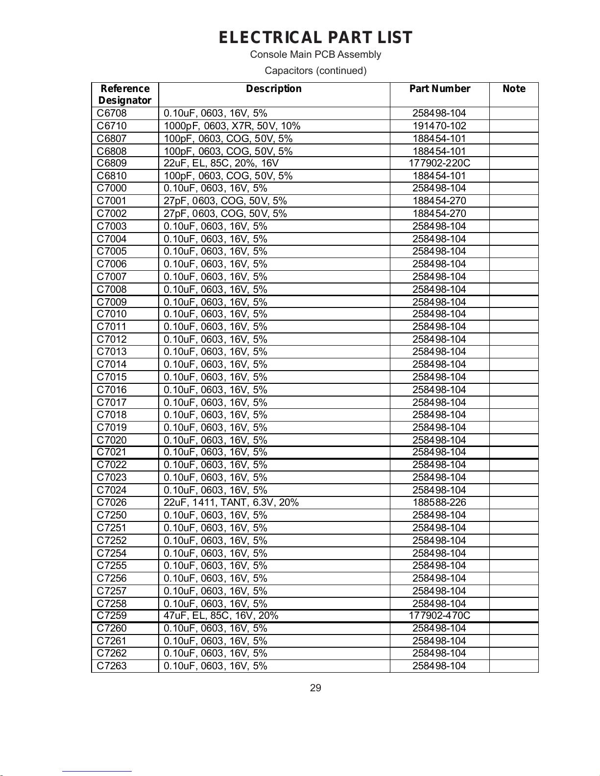
C6708 0.10uF, 0603, 16V, 5% 258498-104
C6710 1000pF, 0603, X7R, 50 V, 10% 191470-102
C6807 100pF, 0603, COG, 50V, 5% 188454-101
C6808 100pF, 0603, COG, 50V, 5% 188454-101
C6809 22uF, EL, 85C, 20%, 16V 177902-220C
C6810 100pF, 0603, COG, 50V, 5% 188454-101
C7000 0.10uF, 0603, 16V, 5% 258498-104
C7001 27pF, 0 603, COG, 50V, 5% 188454-270
C7002 27pF, 0 603, COG, 50V, 5% 188454-270
C7003 0.10uF, 0603, 16V, 5% 258498-104
C7004 0.10uF, 0603, 16V, 5% 258498-104
C7005 0.10uF, 0603, 16V, 5% 258498-104
C7006 0.10uF, 0603, 16V, 5% 258498-104
C7007 0.10uF, 0603, 16V, 5% 258498-104
C7008 0.10uF, 0603, 16V, 5% 258498-104
C7009 0.10uF, 0603, 16V, 5% 258498-104
C7010 0.10uF, 0603, 16V, 5% 258498-104
C7011 0.10uF, 0603, 16V, 5% 258498-104
C7012 0.10uF, 0603, 16V, 5% 258498-104
C7013 0.10uF, 0603, 16V, 5% 258498-104
C7014 0.10uF, 0603, 16V, 5% 258498-104
C7015 0.10uF, 0603, 16V, 5% 258498-104
C7016 0.10uF, 0603, 16V, 5% 258498-104
C7017 0.10uF, 0603, 16V, 5% 258498-104
C7018 0.10uF, 0603, 16V, 5% 258498-104
C7019 0.10uF, 0603, 16V, 5% 258498-104
C7020 0.10uF, 0603, 16V, 5% 258498-104
C7021 0.10uF, 0603, 16V, 5% 258498-104
C7022 0.10uF, 0603, 16V, 5% 258498-104
C7023 0.10uF, 0603, 16V, 5% 258498-104
C7024 0.10uF, 0603, 16V, 5% 258498-104
C7026 22uF, 1411, TANT, 6.3V, 20% 188588-226
C7250 0.10uF, 0603, 16V, 5% 258498-104
C7251 0.10uF, 0603, 16V, 5% 258498-104
C7252 0.10uF, 0603, 16V, 5% 258498-104
C7254 0.10uF, 0603, 16V, 5% 258498-104
C7255 0.10uF, 0603, 16V, 5% 258498-104
C7256 0.10uF, 0603, 16V, 5% 258498-104
C7257 0.10uF, 0603, 16V, 5% 258498-104
C7258 0.10uF, 0603, 16V, 5% 258498-104
C7259 47uF, EL, 85C, 16V, 20% 177902-470C
C7260 0.10uF, 0603, 16V, 5% 258498-104
C7261 0.10uF, 0603, 16V, 5% 258498-104
C7262 0.10uF, 0603, 16V, 5% 258498-104
C7263 0.10uF, 0603, 16V, 5% 258498-104
Page 30

30
ELECTRICAL PART LIST
Capacitors (continued)
Console Main PCB Assembly
Reference
Designator
Description Part Number Note
C7264 0.10uF, 0603, 16V, 5% 258498-104
C7265 0.10uF, 0603, 16V, 5% 258498-104
C7266 0.10uF, 0603, 16V, 5% 258498-104
C7267 0.10uF, 0603, 16V, 5% 258498-104
C7268 0.10uF, 0603, 16V, 5% 258498-104
C7269 0.10uF, 0603, 16V, 5% 258498-104
C7270 0.10uF, 0603, 16V, 5% 258498-104
C7271 0.10uF, 0603, 16V, 5% 258498-104
C7272 0.10uF, 0603, 16V, 5% 258498-104
C8001 0.047uF, 0603, X7R, 25V, 5% 1969 99-473
C8002 0.01uF, 0603, X7R, 50V, 10% 1914 70-103
C8003 0.01uF, 0603, X7R, 50V, 10% 1914 70-103
C8004 0.01uF, 0603, X7R, 50V, 10% 1914 70-103
C8005 33pF, 0 603, COG, 50V, 5% 188454-330
C8006 0.01uF, 0603, X7R, 50V, 10% 1914 70-103
C8013 0.10uF, 0603, 16V, 5% 258498-104
C8014 10uF, EL, 85C, 16V, 20% 177902-100C
C8016 0.10uF, 0603, 16V, 5% 258498-104
C8017 0.10uF, 0603, 16V, 5% 258498-104
C8018 33pF, 0 603, COG, 50V, 5% 188454-330
C8019 100pF, 0805, COG, 50V, 5% 133622-101
C8020 100pF, 0805, COG, 50V, 5% 133622-101
C8021 100pF, 0805, COG, 50V, 5% 133622-101
C8436 0.10uF, 0603, 16V, 5% 258498-104
C8437 1000pF, 0603, X7R, 50 V, 10% 191470-102
C8621 100pF, 0805, COG, 50V, 5% 133622-101
C8622 100pF, 0805, COG, 50V, 5% 133622-101
C8625 0.01uF, 0603, X7R, 50V, 10% 1914 70-103
C9102 0.10uF, 0603, 16V, 5% 258498-104
C9200 0.10uF, 0603, 16V, 5% 258498-104
C9201 10uF, EL, 85C, 16V, 20% 177902-100C
C9202 0.10uF, 0603, 16V, 5% 258498-104
C9203 220pF 0603, COG, 50V, 5% 188454-221
C9204 220pF, 0603, COG, 50V, 5% 188454-221
C9205 470pF, 0603, X7R, 50V, 10% 191470-471
C9206 220pF, 0603, COG, 50V, 5% 188454-221
C9207 220pF, 0603, COG, 50V, 5% 188454-221
C9208 470pF, 0603, X7R, 50V, 10% 191470-471
C9321 .047uF, 0603, X7R, 25V, 5% 196999-473 GSX
C9322 .047uF, 0603, X7R, 25V, 5% 196999-473 GSX
C9323 .047uF, 0603, X7R, 25V, 5% 196999-473 GSX
C9324 4.7uF, EL, 85C, 35V, 20% 177902-4R7V GSX
C9640 .047uF, 0603, X7R, 25V, 5% 196999-473 GSX
C9641 0.10uF, 0603, 16V, 5% 258498-104 GSX
C9642 0.10uF, 0603, 16V, 5% 258498-104 GSX
Page 31

31
Inductors
ELECTRICAL PART LIST
Console Main PCB Assembly
Ferrite Beads
Capacitors (continued)
Reference
Designator
Description Part Number Note
C9643 0.10uF, 0603, 16V, 5% 258498-104 GSX
C9644 0.10uF, 0603, 16V, 5% 258498-104 GSX
C9645 22uF, EL, 85C, 16V, 20% 177902-220C GSX
C9646 0.10uF, 0603, 16V, 5% 258498-104 GSX
C9647 0.10uF, 0603, 16V, 5% 258498-104 GSX
C9648 0.10uF, 0603, 16V, 5% 258498-104 GSX
C9649 0.10uF, 0603, 16V, 5% 258498-104 GSX
C9650 470pF, 0603, X7R, 50V 191470-471 GSX
C9651 180pF, 0603, COG, 50V 1884 54-181 GSX
C9652 2.2pF, 0603,COG,50V, 188454-2R2 GSX
C9653 2.2pF, 0603, COG, 50V 188454-2R2 GSX
Reference
Designator
Description Part Number Note
L1 INDUCTOR, 300uH 180504
L17 INDUCTOR, 300uH 180504
L5000 CERAMIC, 1812, 5%, 1.0 uH 263452-1R0J
L5001 CERAMIC, 1812, 5%, 1.0 uH 263452-1R0J
L5002 CERAMIC, 1812, 5%, 1.0 uH 263452-1R0J
L5003 CERAMIC, 1812, 5%, 1.0 uH 263452-1R0J
L5004 CERAMIC, 1812, 5%, 1.0 uH 263452-1R0J
L5005 CERAMIC, 1812, 5%, 1.0 uH 263452-1R0J
Reference
Designator
Description Part Number Note
FB6200 BEAD, FERRITE, 0805, 1.5A, 330 OHM 267539-331
FB7000 BEAD, FERRITE, 0805, 1.5A, 330 OHM 267539-331
FB7001 BEAD, FERRITE, 0805, 1.5A, 330 OHM 267539-331
FB7002 BEAD, FERRITE, 0805, 1.5A, 330 OHM 267539-331
FB7250 BEAD, FERRITE, 0805, 1.5A, 330 OHM 267539-331
FB7251 BEAD, FERRITE, 0805, 1.5A, 330 OHM 267539-331
FB7252 BEAD, FERRITE, 0805, 1.5A, 330 OHM 267539-331
FB7253 BEAD, FERRITE, 0805, 1.5A, 330 OHM 267539-331
Page 32

32
ELECTRICAL PART LIST
Transistors
Console Main PCB Assembly
Diodes
Reference
Designator
Description Part Number Note
D1 SCHOTTKY, 40V, 3A, SMB 193847-001
D17 SCHOTTKY, 40V, 3A, SMB 1938 47-001
D4000 DUAL, SOT-23, BAV99 147239
D4202 DUAL, SOT-23, BAV99 147239
D5000 DUAL, SOT-23, BAV99 147239
D5001 DUAL, SOT-23, BAV99 147239
D5002 DUAL, SOT-23, BAV99 147239
D5003 DUAL, SOT-23, BAV99 147239
D6302 DUAL, SOT-23, BAV99 147239
D6500 DUAL, SOT-23, BAV99 147239
D6701 DUAL, SOT-23, BAV99 147239
D6702 DUAL, SOT-23, BAV99 147239
D6703 DUAL, SOT-23, BAV99 147239
D6704 DUAL, SOT-23, BAV99 147239
D6705 DUAL, SOT-23, BAV99 147239
D6800 DUAL, SOT-23, BAV99 147239
D6801 DUAL, SOT-23, BAV99 147239
D7000 DUAL, SOT-23, BAV99 147239
D7001 DUAL, SOT-23, BAV99 147239
D8000 DUAL, SOT-23, BAV99 147239
D8001 DUAL, SOT-23, BAV99 147239
D8002 DUAL, SOT-23, BAV99 147239
D8600 DUAL, SOT-23, BAV99 147239
Reference
Designator
Description Part Number Note
Q1 SENSOR, IR, SMT 270841-001
Q2 BPLR, P, 40V, 200mA, SOT23 148596
Q3 BPLR, N, 50V, 100mA, SOT23 146817
Q4 BPLR, P, 40V, 200mA, SOT23 148596
Q5 BPLR, N, 40V, 200mA, SOT23 146819
Q3200 BPLR, N, 50V, 10 0mA, SOT23 146817
Q4000 BPLR, P, 40V, 200mA, SOT23 148596
Q4201 P, 50V, 2SA1341 146818
Q4202 BPLR, N, 4.7K, SOT23 192603
Q4208 BPLR, P, 40V, 200mA, SOT23 148596
Q4209 BPLR, P, 40V, 200mA, SOT23 148596
Q5000 BPLR, N, 40V, 20 0mA, SOT23 146819
Q6300 BPLR, N, 50V, 10 0mA, SOT23 146817
Q6301 BPLR, N, 50V, 10 0mA, SOT23 146817
Q6302 P, 50V, 2SA1341 146818
Q6503 N, SOT-23, MMBT4403 260354-001
Q6504 BPLR, N, 4.7K, SOT23 192603
Q6802 BPLR, P, 40V, 200mA, SOT23 148596
Page 33

33
ELECTRICAL PART LIST
Console Main PCB Assembly
Integrated Circuits
Transistors (continued)
Reference
Designator
Description Part Number Note
Q6803 BPLR, N, 40V, 20 0mA, SOT23 146819
Q6804 BPLR, N, 40V, 20 0mA, SOT23 146819
Q6805 BPLR, P, 40V, 200mA, SOT23 148596
Q9100 BPLR, N, 40V, 20 0mA, SOT23 146819
Q9101 BPLR, N, 40V, 20 0mA, SOT23 146819
Q9102 BPLR, N, 40V, 20 0mA, SOT23 146819
Reference
Designator
Description Part Number Note
VR1 VREG, POS, D2 PAK, LD1086, 3.3V 260638- 33
VR2 VREG, POS, D2 PAK, LD1086, 1.8V 260638- 18
U2 VOLT REG, 3.3V, 3.5A, SMPS 193846-001
U3 COUNTER, BINARY, 8-BIT, TSSOP 256115-002
U17 VOLT REG, 3.3V, 3.5A, SMPS 1938 46-001
U19 9V VOLTAGE REGULATOR 258167-09
U4000 AUDIO MATRIX, SO28 177984-2
U6200 SDRAM, 128 MBIT, 166 MHZ 267336-001 STD/GS
U6200 SDRAM, 256 MBIT, 166 MHZ, TSSOP 274511-001 GSX
U6203 FLASH, PROGRAMMED, 4 MBYTE, TSSOP 307633 STD/GS
U6203 FLASH, PROGRAMMED, 4 MBYTE, TSSOP 307634 GSX
U6204 16 BIT BUS BUFFER, 74LCX16245 267613-001
U6205 16 BIT BUS BUFFER, 74LCX16245 267613-001
U6802 HEX BUFFER, CMOS 267619-001
U7002 RESET, SC70 267095-001
U7003 CS98200 266925-001
U8001 S/PDIF RCVR, AK4112B 270223
U8002 QUAD, SOIC 193858-004
U8405 OP AMP, DUAL, HI CURRENT 256741-001
U8406 QUAD OP AMP, TLO74D, SOIC 186112
U9100 OP AMP, DUAL, HI CURRENT 256741-001
U9200 DAC, 192 KHZ, 24 BIT, AK4382 267548-001
U9201 OP AMP, DUAL, HI CURRENT 256741-001
U9641 ETHERNET CONTROLLER 2688 67-001 GSX
Page 34

34
Miscellaneous
ELECTRICAL PART LIST
Console Main PCB Assembly
Reference
Designator
Description Part Number Note
J1 CO NN, SMT, LIF, 4 POS, SIDE 255130-004
J2 CO NN, SMT, LIF, 4 POS, SIDE 255130-004
J3 CO NN, SMT, LIF, 9 POS, SIDE 255130-009
J100 CONN, 13-PIN SOCKET, R-ANGLE 270581-001
J201 CO NN, RCA BLOCK, W/GRND FLANGE 279923-002
J202 CO NN, DIN, 9 POS, SINGLE 269854-001
J3200 CONN, H EADER, 40 PIN 256 105-001
J3202 CONN, HEADER, 4 POS 148591 -04
J6000 CONN, H EADER, 13 POS, TOP-ENTRY, SMT 253356-T13
J6500 CONN, H EADER, 5 POS, TOP ENTRY, SMD 25335 6-T05
J6700 CONN, H EADER, 9 POS, TOP ENTRY, SMD 25335 6-T09
J8000 CONN, OPTICAL, JFJ2001 258421-001
J9341 CONNECTOR, EJECTOR, EHT, HDD 256109-44 GSX
J9640 CONN, ETHERNET, W/XFMR & LED 272162-002 GSX
K5000 RELAY, FLAT, POLARIZED 267094-001
K5001 RELAY, FLAT, POLARIZED 267094-001
T8600 TRANSFORMER, PULSE 254185-001
XJ1 SHIELD, SUPPORT, 13P, SQR, CONN 278839-001
Y7000 CRYSTAL, 27 MHZ, 3 0 PPM, HC-49/U/S 256102-005
Y8000 CRYSTAL, 11.2896 MHZ, HC49S, SMD 197225
Y9640 CRYSTAL, 20.0 MHZ, 18pF, HC49S, SMD 268 873-005 GSX
- TAPE, SHIELDING, ALUMINUM 279013-0 01
- GASKET, EMI, BOSELINK 279058-001
- HEATSINK, DSP 270920-001
Page 35

35
Resistors
ELECTRICAL PART LIST
Console Tuner PCB Assembly
Reference
Designator
Description Part Number Note
R2000 1K, 0603, .1W, 5% 199403-102 4
R2001 120 OHM, 0603, .1W , 5% 199403-121 4
R2002 150 OHM, 0603, .1W , 5% 199403-151 4
R2003 100K, 0603, .1W, 5% 199403-104 4
R2004 47K, 0603, .1W , 5% 199403-473 4
R2005 2.32K, 0603, .1W, 1% 1914 65-2321 4
R2006 499 OHM, 0603, .1W , 1% 191465-4990 4
R2007 2.32K, 0603, .1W, 1% 1914 65-2321 4
R2008 330 OHM, 0603, .1W , 1% 191465-3300 4
R2009 1.18K, 0603, 1 00MW, 1% 191465-1181 4
R2010 22 OHM, 0603, .1W, 5% 199403-220 4
R2011 4.75K, 0603, .1W, 1% 1914 65-4751 4
R2012 100 OHM, 0603, .1W , 5% 199403-101 4
R2013 17.8K, 0603, 0.1W, 1 % 191465-1782 4
R2014 51 OHM, 0603, 100MW, 5% 199403- 510 4
R2015 2.32K, 0603, .1W, 1% 1914 65-2321 4
R2016 3.01K, 0603, .1W, 1% 1914 65-3011 4
R2017 5.1K, 0603, .1W, 5% 199403-512 4
R2018 5.1K, 0603, .1W, 5% 199403-512 4
R2019 51 OHM, 0603, 100MW, 5% 199403- 510 4
R2020 13K, 0603, .1W , 1% 1914 65-1302 4
R2021 17.8K, 0603, 0.1W, 1 % 191465-1782 4
R2022 3.32K, 0603, .1W, 1% 1914 65-3321 4
R2023 3.32K, 0603, .1W, 1% 1914 65-3321 4
R2024 2.21K, 0603, .1W, 1% 1914 65-2211 4
R2025 2.21K, 0603, .1W, 1% 1914 65-2211 4
R2026 4.75K, 0603, .1W, 1% 1914 65-4751 4
R2027 5.62K, 0603, 1 00MW, 1% 191465-5621 4
R2028 5.62K, 0603, 1 00MW, 1% 191465-5621 4
R2030 68.1K, 0603, .1W, 1% 1914 65-6812 4
R2031 4.75K, 0603, .1W, 1% 1914 65-4751 4
R2032 3.01K, 0603, .1W, 1% 1914 65-3011 4
R2033 33.2K, 0603, .1W, 1% 1914 65-3322 4
R2034 3.32K, 0603, .1W, 1% (EURO) 1914 65-3321 4
R2034 3.32K, 0603, .1W, 1% (JAPAN) 191465-332 1 4
R2073 1K, 0603, .1W, 5% 199403-102 4
R2074 1K, 0603, .1W, 5% 199403-102 4
R2075 100 OHM, 0603, .1W , 5% 199403-101 4
R2076 2.2K, 0603, .1W, 5% 199403-222 4
R2077 6.81K, 0603, .1W, 1% 1914 65-6811 4
R2078 3.01K, 0603, .1W, 1% 1914 65-3011 4
R2079 2.0K, 0603, .1W, 5% 199403-202 4
R2080 3.32K, 0603, .1W, 1% 1914 65-3321 4
R2081 1K, 0603, .1W, 1% 191465-1001 4
R2082 1K, 0603, .1W, 5% 199403-102 4
R2083 51 OHM, 0603, 100MW, 5% 199403- 510 4
R2084 1K, 0603, .1W, 1% 191465-1001 4
Page 36

36
Resistors (continued)
ELECTRICAL PART LIST
Console Tuner PCB Assembly
Capacitors
Reference
Designator
Description Part Number Note
R2085 3.32K, 0603, .1W, 1% 1914 65-3321 4
R2090 100K, 0603, .1W, 5% 199403-104 4
R2200 2.0K, 0603, .1W, 5% 199403-202 4
R2201 2.0K, 0603, .1W, 5% 199403-202 4
R2202 2.0K, 0603, .1W, 5% 199403-202 4
R2203 2.0K, 0603, .1W, 5% 199403-202 4
R2204 20 OHM, 0603, .1W, 5% (EURO) 199403-200 4
R2205 20 OHM, 0603, .1W, 5% (EURO) 199403-200 4
R7000 1.5K, 0603, SMD, 100MW, 5% 199403-152 4
R7001 1K, 0603, .1W, 5% 199403-102 4
R7003 100 OHM, 0603, .1W , 5% 199403-101 4
R7004 100 OHM, 0603, .1W , 5% 199403-101 4
R7006 100 OHM, 0603, .1W , 5% 199403-101 4
R7007 100 OHM, 0603, .1W , 5% 199403-101 4
R7008 17.8K, 0603, 0.1W, 1 % 191465-1782 4
R7009 10K, 0603, .1W , 5% 199403-103 4
R7011 2.21K, 0603, .1W, 1% 1914 65-2211 4
R7012 2.21K, 0603, .1W, 1% 1914 65-2211 4
R7013 100 OHM, 0603, .1W , 5% 199403-101 4
R7014 100 OHM, 0603, .1W , 5% 199403-101 4
R7015 100 OHM, 0603, .1W , 5% 199403-101 4
R7016 100 OHM, 0603, .1W , 5% 199403-101 4
R7017 100 OHM, 0603, .1W , 5% 199403-101 4
R7018 51 OHM, 0603, 100MW, 5% 199403- 510 4
Reference
Designator
Description Part Number Note
C17 10uF, EL, 85 C, 16V, 20% 177902-100C 4
C28 10uF, EL, 85 C, 16V, 20% 177902-100C 4
C29 .047uF, 0805, X7R, 50V, 10% 133623-473 4
C30 .047uF, 0805, X7R, 50V, 10% 133623-473 4
C2000 12pF, 0805, COG, 50V, 5% 133622-120 4
C2001 .047uF, 080 5, X7R, 50V, 10% 133623-473 4
C2002 .047uF, 080 5, X7R, 50V, 10% 133623-473 4
C2003 9.1pF, 0603, COG, 50V 188454-9R1 4
C2004 .047uF, 080 5, X7R, 50V, 10% 133623-473 4
C2005 2.2uF, EL, 85C, 35V, 20% 177 902-2R2V 4
C2006 .047uF, 080 5, X7R, 50V, 10% 133623-473 4
C2007 .047uF, 080 5, X7R, 50V, 10% 133623-473 4
C2008 47uF, EL, 85C, 16V, 20% 177902-470C 4
C2009 .047uF, 080 5, X7R, 50V, 10% 133623-473 4
C2010 .47uF, 1206, X7R, 16V 181998-474 4
C2011 47uF, EL, 85C, 16V, 20% 177902-470C 4
C2012 1uF, EL, 85C, 50V, 20% 177902-010H 4
C2013 180pF, 0603, COG, 50V 188454-181 4
C2014 1uF, EL, 85C, 50V, 20% 177902-010H 4
Page 37

37
Capacitors (continued)
ELECTRICAL PART LIST
Console Tuner PCB Assembly
Inductors
Reference
Designator
Description Part Number Note
C2015 1uF, EL, 85C, 50V, 20% 177902-010H 4
C2016 .47uF, EL, 85C, 50V, 20% 177902 -R47H 4
C2017 22uF, EL, 85C, 20%, 16V 177902-220C 4
C2018 560pF, 0603, X7R, 50V 191470-561 4
C2019 47uF, EL, 85C, 16V, 20% 177902-470C 4
C2020 .01uF, 0603, X7R, 50V 191470-103 4
C2021 10uF, EL, 85C, 16V, 20% 177902-100C 4
C2022 10uF, EL, 85C, 16V, 20% 177902-100C 4
C2023 10uF, EL, 85C, 16V, 20% 177902-100C 4
C2024 .047uF, 080 5, X7R, 50V, 10% 133623-473 4
C2025 3.3uF, EL, 85C, 35V, 20% 177 902-3R3V 4
C2026 .047uF, 0603, X7R, 5%, 25V (US) 196999- 473 4
C2026 .033uF, 0603, X7R, 25V
(
EURO /J APAN) 196999-333 4
C2027 .047uF, 0603, X7R, 5%, 25V (US) 196999- 473 4
C2027 .033uF, 0603, X7R, 25V (EURO/JAPAN) 196999-333 4
C2073 .047uF, 0603, X7R, 5%, 25V 196999-473 4
C2094 100uF, EL, 8 5C, 16V, 20% 177902-101C 4
C2095 .047uF, 0603, X7R, 5%, 25V 196999-473 4
C2096 2.2uF, EL, BP, 85C, 50V, 20% 147522-2R2 4
C2097 .01uF, 0603, X7R, 50V 191470-103 4
C2098 1000pF, 0603, X7R, 5 0V 191470-102 4
C2099 1000pF, 0603, X7R, 5 0V 191470-102 4
C2100 .047uF, 0603, X7R, 5%, 25V 196999-473 4
C2200 100pF, 0603, COG, 50V, 5 % 188454-101 4
C2201 .047uF, 080 5, X7R, 50V, 10% (EURO) 133623-473 4
C2202 560pF, 0603, COG, 50V, 5 % (EURO) 188454-561 4
C2203 330pF, 0603, COG, 50V, 5 % (EURO) 188454-331 4
C2204 10uF, EL, 85C, 16V, 20% (EURO) 177902-100C 4
C2205 22pF, 0603, COG, 50V, 5% (EURO) 188454-220 4
C2206 22pF, 0603, COG, 50V, 5% (EURO) 188454-220 4
C2207 0.1uF, 0805, X7R, 50V (EURO) 133624 4
C7000 .047uF, 080 5, X7R, 50V, 10% 133623-473 4
C7001 1000pF, 0603, X7R, 5 0V 191470-102 4
C7002 47pF, 0603, COG, 50V, 5% 188454-470 4
C7003 .047uF, 0603, X7R, 5%, 25V 196999-473 4
C7004 47pF, 0603, COG, 50V, 5% 188454-470 4
C7006 .047uF, 0603, X7R, 5%, 25V 196999-473 4
C7007 10uF, EL, 85C, 16V, 20% 177902-100C 4
Reference
Designator
Description Part Number Note
L2000
A
X ON ALR, 1000uH, 40A 260363-102 4
L7000 INDUCTOR, 0805, 5%, 470nH 291122-471J 4
Page 38

38
ELECTRICAL PART LIST
Console Tuner PCB Assembly
Transistors
Integrated Circuits
Miscellaneous
Diodes
Reference
Designator
Description Part Number Note
D2075 SOT-23, BAV 99 147239 4
Reference
Designator
Description Part Number Note
Q2000 P, 50V, 2SA1341 146818 4
Q2001 BPLR, N, 25 V, 30MA, SOT-23 187601-001 4
Q2002 JFET, N, 20V, 20mA, TO-92 148590-E 4
Q2003 BPLR, N, 40 V, 200mA, SOT23 (EURO) 146819 4
Q2073 BPLR, N, 40 V, 200mA, SOT23 146819 4
Q7000 P, 50V, 2SA1341 146818 4
Q7001 BPLR, N, 50 V, 100mA, SOT23 146817 4
Reference
Designator
Description Part Number Note
U18 VOLT REG, SMD, POS, SOT89, +10V 258167-10
U19 VOLT REG, SMD, POS, SOT89, +5V 258167-05
U2000 AM/FM TUNER, MFP-30S 254561-001
U2074 PLL FREQ SYNTH, MFP-24 199693
U2200 RDS, SIGNAL PROCESSOR 254562-001 EURO
U7000 EEPROM, SO-8, 24C01A 184044
Reference
Designator
Description Part Number Note
CF2000 FILTER, CER, BANDPASS, FGD, 280KHZ 253037- 002
CF2001 FILTER, CER, BANDPASS, FGD, 220KHZ 253037- 001
FM-TNR2000 TUNER, FM, US 258513-001 U S
FM-TNR2000 TUNER, FM, 7V, EU RO 258513-003 EURO
FM-TNR2000 TUNER, FM, JAPAN 258513-002 JAPAN
J1 CONN, HEADER, 13P, TOP-ENTRY, SMT 253 356-T13
J2000 CONN, AM ANTENNA 289460- 001
J2001 CONN, FM, SHIELDED, US 258434-001
SHLD -
TNR2000
SHIELD, FENCE, TUNER 256743 4
T2000 TUNER, AM, FRONT END 310458-001
T2001 FILTER, AM-IF, QUINTIPLE TUNED 254114-001
T2002 DETEC TOR, FM, SINGLE TUNED 254564-001
Y2200 CRYSTAL, QUARTZ, 4.332MHZ, 50PPM 254563- 001 EURO
Y7000 XTAL, 14.4MHZ, 30pF, HC49S, SMD 267620-005
- SHIELD, COVER, TUNER 256744 4
Page 39

39
ELECTRICAL PART LIST
Bass Module DSP/Amplifier PCB Assembly
Resistors
Reference
Designator
Description Part Number Note
R8 1.00K, 0805, 1/10W, 5% 133626-1025
R9 3.30K, 0805, 1/10W, 5% 133626-3325
R10 10.0K, 0805, 1/10W, 5% 133626-1035
R12 1.00K, 0805, 1/10W, 5% 133626-1025
R13 20.0K, 0805, 1/10W, 5% 133626-2035
R14 1.69K, 0603, 1/10W, 1% 191465-1691
R15 3.32K, 0603, 1/10W, 1% 191465-3321
R16 49.9K, 0603, 1/10W, 1% 191465-4992
R17 10K, 0603, 1/10W, 1% 191465-1002
R18 100K, 0603, 1/10W, 5% 199403-104
R19 56K, 0603, 1/10W, 5% 199403-563
R20 10.0K, 0805, 1/10W, 5% 133626-1035
R21 240K, 0603, 1/10W, 5% 199403-244
R22 33.0K, 0805, 1/10W, 5% 133626-3335
R23 10 OHM, 2512, 1W, 5% 181895-10R0
R24 1 MEG, 1206, 1/4W, 5% 124895-1055
R25 1 MEG, 1206, 1/4W, 5% 124895-1055
R26 1 MEG, 1206, 1/4W, 5% 124895-1055
R150 3.9K, ARRAY, SMT, 4 POS, 5% 186433-3924
R151 7.87K, 0603, 1/10W, 1% 191465-7871
R152 7.87K, 0603, 1/10W, 1% 191465-7871
R162 3.32 OHM, 0603, 1/10W, 1% 191465-3R32
R163 3.32 OHM, 0603, 1/10W, 1% 191465-3R32
R164 3.32 OHM, 0603, 1/10W, 1% 191465-3R32
R165 3.32 OHM, 0603, 1/10W, 1% 191465-3R32
R250 3.9K, ARRAY, SMT, 4 POS, 5% 186433-3924
R251 7.87K, 0603, 1/10W, 1% 191465-7871
R252 7.87K, 0603, 1/10W, 1% 191465-7871
R262 3.32 OHM, 0603, 1/10W, 1% 191465-3R32
R263 3.32 OHM, 0603, 1/10W, 1% 191465-3R32
R264 3.32 OHM, 0603, 1/10W, 1% 191465-3R32
R265 3.32 OHM, 0603, 1/10W, 1% 191465-3R32
R350 3.9K, ARRAY, SMT, 4 POS, 5% 186433-3924
R351 7.87K, 0603, 1/10W, 1% 191465-7871
R362 3.32 OHM, 0603, 1/10W, 1% 191465-3R32
R363 3.32 OHM, 0603, 1/10W, 1% 191465-3R32
R364 3.32 OHM, 0603, 1/10W, 1% 191465-3R32
R365 3.32 OHM, 0603, 1/10W, 1% 191465-3R32
R450 15K, 0603, 1/10W, 5% 199403-153
R451 47K, 0603, 1/10W, 5% 199403-473
R452 4.7K, 0603, 1/10W, 5% 199403-472
R453 1.69K, 0603, 1/10W, 1% 191465-1691
R454 4.7K, 0603, 1/10W, 5% 199403-472
R455 1.21K, 0603, 1/10W, 1%
(US/CANADA UNITS BUILT BEFORE 3/1/05)
191465-1211
R456 240K, 0603, 1/10W, 5% 199403-244
R457 240K, 0603, 1/10W, 5% 199403-244
Page 40

40
ELECTRICAL PART LIST
Bass Module DSP/Amplifier PCB Assembly
Resistors (continued)
Reference
Designator
Description Part Number Note
R1001 510 OHM, ARRAY, SMT, 4 POS, 5% 186433-5114
R1005 510 OHM, ARRAY, SMT, 4 POS, 5% 186433-5114
R4200 4.7K, 0603, 1/10W, 5% 199403-472
R4201 75 OHM, 0603, 1/10W, 5% 199403-750
R4202 75 OHM, 0603, 1/10W, 5% 199403-750
R4203 75 OHM, 0603, 1/10W, 5% 199403-750
R4204 10K, 0603, 1/10W, 5% 199403-103
R4300 1.8K, ARRAY, SMT, 4 POS, 5% 186433-1824
R4301 1.8K, ARRAY, SMT, 4 POS, 5% 186433-1824
R4302 1.8K, ARRAY, SMT, 4 POS, 5% 186433-1824
R4500 100 OHM, 0603, 1/10W, 5% 199403-101
R4501 100 OHM, 0603, 1/10W, 5% 199403-101
R4503 100 OHM, 0603, 1/10W, 5% 199403-101
R4505 100 OHM, 0603, 1/10W, 5% 199403-101
R4600 1.21K, 0603, 1/10W, 1% 191465-1211
R4602 47K, 0603, 1/10W, 5% 199403-473
R4603 47K, 0603, 1/10W, 5% 199403-473
R4604 47K, 0603, 1/10W, 5% 199403-473
R4700 4.7K, 0603, 1/10W, 5% 199403-472
R4701 75 OHM, 0603, 1/10W, 5% 199403-750
R6000 3.3K, 0603, 1/10W, 5% 199403-332
R6001 1.00K, 0805, 1/10W, 5% 133626-1025
R6100 2.0K, 0603, 1/10W, 5% 199403-202
R6101 10K, 0603, 1/10W, 5% 199403-103
R6102 2.7K, 0603, 1/10W, 5% 199403-272
R6103 300 OHM, 0603, 1/10W, 5% 199403-301
R6104 75 OHM, 0603, 1/10W, 5% 199403-750
R6105 75 OHM, 0603, 1/10W, 5% 199403-750
R6500 330 OHM, 0603, 1/10W, 5% 199403-331
R6502 1K, 0603, 1/10W, 5% 199403-102
R7000 470 OHM, 0603, 1/10W, 5% 199403-471
R7001 22 OHM, 0603, 1/10W, 5% 199403-220
R7100 75 OHM, 0603, 1/10W,,5% 199403-750
R7102 4.7K, 0603, 1/10W, 5% 199403-472
R7103 4.7K, 0603, 1/10W, 5% 199403-472
R7104 75 OHM, 0603, 1/10W, 5% 199403-750
R7105 75 OHM, 0603, 1/10W, 5% 199403-750
R7106 75 OHM, 0603, 1/10W, 5% 199403-750
R7107 2.0K, 0603, 1/10W, 5% 199403-202
R7108 75 OHM, 0603, 1/10W, 5% 199403-750
R7109 75 OHM, 0603, 1/10W, 5% 199403-750
R7110 75 OHM, 0603, 1/10W, 5% 199403-750
R7111 75 OHM, 0603, 1/10W, 5% 199403-750
R7112 75 OHM, 0603, 1/10W, 5% 199403-750
R7113 75 OHM, 0603, 1/10W, 5% 199403-750
R7114 75 OHM, 0603, 1/10W, 5% 199403-750
R7200 100K, 0603, 1/10W, 5% 199403-104
Page 41

41
ELECTRICAL PART LIST
Bass Module DSP/Amplifier PCB Assembly
Resistors (continued)
Capacitors
Reference
Designator
Description Part Number Note
R7201 10K, 0603, 1/10W, 5% 199403-103
R7202 4.7K, 0603, 1/10W, 5% 199403-472
R7203 4.7K, 0603, 1/10W, 5% 199403-472
R7204 47 OHM, 0603, 1/10W, 5% 199403-470
R7205 1M, 0603, 1/10W, 5% 199403-105
R7206 10K, 0603, 1/10W, 5% 199403-103
R7207 4.7K, 0603, 1/10W, 5% 199403-472
Reference
Designator
Description Part Number Note
-- 22uF, EL, 85C, 50V, 20% [atJ150 pins 9 & 10]
(ALL UNITS BUILT AFTER 3/1/05)
149948-220H
C21 4700pF, 0603, X7 R, 50V, 10% 191470-472
C22 15000uF, EL, 105 C, 25V, 20% 261614-153EB3
C24 .022uF, 0603, X7R, 50V, 10% 191470-223
C26 .047uF, 0805, X7R, 50V, 10% 286499-473
C27 .047uF, 0805, X7R, 50V, 10% 286499-473
C28 .047uF, 0805, X7R, 50V, 10% 286499-473
C29 .047uF, 0805, X7R, 50V, 10% 286499-473
C30 2 20uF, EL, SMD, 105C, 10V, 20 % 256772-221A
C31 2 20uF, EL, SMD, 105C, 10V, 20 % 256772-221A
C32 47uF, EL, SMD, 105C, 35V, 20% 255 071-470V
C33 1000pF, 0603, X7 R, 50V, 10% 191470-102
C34 .015uF, 0603, X7R, 50V, 10% 191470-153
C35 .22uF, TANT, 35V, 20%, ASIZE 262073-V224A
C36 .1uF, 12 06, X7R, 25V, 5% 131754-104
C37 .01uF, 0 603, X7R, 50V, 10% 191470-103
C38 .047uF, 0603, X7R, 50V, 10% 191470-473
C39 .047uF, 0603, X7R, 50V, 10% 191470-473
C40 150pF, 0603, COG, 50V, 5% 188454-151
C41 .047uF, 0603, X7R, 50V, 10% 191470-473
C42 2.2uF, TANT, 10V, 20%, ASIZE 19 6981-A225A2
C43 4700pF, 0603, X7 R, 50V, 10% 191470-472
C44 .047uF, 0603, X7R, 50V, 10% 191470-473
C46 4700pF, 0603, X7 R, 50V, 10% 191470-472
C47 3300pF, 0805, X7 R, 50V, 10% 133623-332
C48 1.0uF, 1 206, X7R, 25V, 15% 262063-105
C49 1.0uF, 1 206, X7R, 25V, 15% 262063-105
C52 1.0uF, 1 206, X7R, 25V, 15% 262063-105
C53 1000pF, 0603, X7 R, 50V, 10% 191470-102
C56 47pF, 0603, COG, 50V, 5% 188454- 470
C57 47pF, 0603, COG, 50V, 5% 188454- 470
C58 470pF, 0603, X7R , 50V, 10% 191470-471
C59 470pF, 0603, X7R , 50V, 10% 191470-471
C60 470pF, 0603, X7R , 50V, 10% 191470-471
Page 42

42
ELECTRICAL PART LIST
Bass Module DSP/Amplifier PCB Assembly
Capacitors (continued)
Reference
Designator
Description Part Number Note
C61 470pF, 0603, X7R , 50V, 10% 191470-471
C62 2.2u F, FILM, 100V, 10% 260333-22 5A
C63 47uF, EL, SMD, 105C, 50V, 20%
(USED ON UNITS BUILT AFTER 4/1/05)
255071-470H
C150 1 00uF, EL, 85C, 25V, 20% 177902-10 1E
C151 .047uF, 0805, X7R, 50V, 10% 286499-473
C152 .01uF, 0603, X7R, 50V, 10% 191470-103
C153 .01uF, 0603, X7R, 50V, 10% 191470-103
C154 .01uF, 0603, X7R, 50V, 10% 191470-103
C155 .01uF, 0603, X7R, 50V, 10% 191470-103
C156 1 uF, EL, 85C, 50V, 20% 177902-010H
C157 1 uF, EL, 85C, 50V, 20% 177902-010H
C158 1 000pF, 0805, COG, 50V, 5% 286499-102
C159 1 uF, EL, 85C, 50V, 20% 177902-010H
C160 1 uF, EL, 85C, 50V, 20% 177902-010H
C161 1 000pF, 0805, COG, 50V, 5% 286499-102
C250 1 00uF, EL, 85C, 25V, 20% 177902-10 1E
C251 .047uF, 0805, X7R, 50V, 10% 286499-473
C252 .01uF, 0603, X7R, 50V, 10% 191470-103
C253 .01uF, 0603, X7R, 50V, 10% 191470-103
C254 .01uF, 0603, X7R, 50V, 10% 191470-103
C255 .01uF, 0603, X7R, 50V, 10% 191470-103
C256 1 uF, EL, 85C, 50V, 20% 177902-010H
C257 1 uF, EL, 85C, 50V, 20% 177902-010H
C258 1 000pF, 0805, COG, 50V, 5% 286499-102
C259 1 uF, EL, 85C, 50V, 20% 177902-010H
C260 1 uF, EL, 85C, 50V, 20% 177902-010H
C261 1 000pF, 0805, COG, 50V, 5% 286499-102
C350 1 00uF, EL, 85C, 25V, 20% 177902-10 1E
C351 .047uF, 0805, X7R, 50V, 10% 286499-473
C352 .01uF, 0603, X7R, 50V, 10% 191470-103
C353 .01uF, 0603, X7R, 50V, 10% 191470-103
C354 .01uF, 0603, X7R, 50V, 10% 191470-103
C355 .01uF, 0603, X7R, 50V, 10% 191470-103
C356 1 uF, EL, 85C, 50V, 20% 177902-010H
C357 1 uF, EL, 85C, 50V, 20% 177902-010H
C358 1 000pF, 0805, COG, 50V, 5% 286499-102
C359 4 700pF, 0603, X7 R, 50V, 10% 191470-472
C360 4 70pF, 0603, COG, 50V, 5% 188454-471
C361 4 70pF, 0603, COG, 50V, 5% 188454-471
C362 4 70pF, 0603, COG, 50V, 5% 188454-471
C363 4 70pF, 0603, COG, 50V, 5% 188454-471
C364 1 000pF, 0805, COG, 50V, 5% 286499-102
C365 .047uF, 0603, X7R, 50V, 10% 191470-473
C1000 1 000pF, 0603, X7R, 50V, 10% 191470- 102
C1001 1 000pF, 0603, X7R, 50V, 10% 191470- 102
Page 43

43
ELECTRICAL PART LIST
Bass Module DSP/Amplifier PCB Assembly
Capacitors (continued)
Reference
Desi gnator
Description Part Number Note
C1002 1000pF, 0603, X7R, 50V, 10% 191470-102
C1003 1 000pF, 0603, X7R, 50V, 10% 191470-102
C4000 2 2uF, EL, 85C, 16V, 20% 177902-220C
C4001 .047uF, 0603, X7R, 50V, 10% 191470-473
C4002 .047uF, 0603, X7R, 50V, 10% 191470-473
C4003 .047uF, 0603, X7R, 50V, 10% 191470-473
C4104 2200pF, 0603, X7R, 50V, 10% 191470-222
C4105 2 200pF, 0603, X7R, 50V, 10% 191470-222
C4200 1 0uF, EL, 85C, 16V, 20% 177902-100C
C4300 1000pF, 0603, X7R, 50V, 10% 191470-102
C4301 1 000pF, 0603, X7R, 50V, 10% 191470-102
C4302 1 000pF, 0603, X7R, 50V, 10% 191470-102
C4303 1000pF, 0603, X7R, 50V, 10% 191470-102
C4304 1 000pF, 0603, X7R, 50V, 10% 191470-102
C4306 1 000pF, 0603, X7R, 50V, 10% 191470-102
C4307 1000pF, 0603, X7R, 50V, 10% 191470-102
C4308 1 000pF, 0603, X7R, 50V, 10% 191470-102
C4308 1 000pF, 0603, X7R, 50V, 10% 191470-102
C4309 1000pF, 0603, X7R, 50V, 10% 191470-102
C4309 1 000pF, 0603, X7R, 50V, 10% 191470-102
C4310 1 000pF, 0603, X7R, 50V, 10% 191470-102
C4310 1 000pF, 0603, X7R, 50V, 10% 191470-102
C4400 .047uF, 0603, X7R, 50V, 10% 191470-473
C4401 .047uF, 0603, X7R, 50V, 10% 191470-473
C4500 68pF, 0603, COG, 50V, 5% 188454-680
C4501 6 8pF, 0603, COG, 50V, 5% 188454-680
C4600 .047uF, 0603, X7R, 25V, 5% 196999-473
C4601 4700pF, 0603, X7R, 50V, 10% 191470-472
C4602 .047uF, 0603, X7R, 25V, 5% 196999-473
C6000 .047uF, 0603, X7R, 50V, 10% 191470-473
C6100 .047uF, 0603, X7R, 50V, 10% 191470-473
C6101 4 700pF, 0603, X7R, 50V, 10%
(US/CANADA UNITS BUILT BEFORE 3/1/05)
191470-472
C6101 .022uF, 0603, X7R, 50V, 10%
(ALL UNITS BUILT AFTER 3/1/05)
191470-223
C6102 1 000pF, 0603, X7R, 50V, 10% 191470-102
C6105 8 20pF, 0603, X7R, 50V, 10% 191470- 821
C6500 4 700pF, 0603, X7R, 50V, 10% 191470-472
C7000 .047uF, 0603, X7R, 50V, 10% 191470-473
C7001 .047uF, 0603, X7R, 50V, 10% 191470-473
C7002 .047uF, 0603, X7R, 50V, 10% 191470-473
C7003 .047uF, 0603, X7R, 50V, 10% 191470-473
C7004 .047uF, 0603, X7R, 50V, 10% 191470-473
C7005 .047uF, 0603, X7R, 50V, 10% 191470-473
C7006 .047uF, 0603, X7R, 50V, 10% 191470-473
C7007 .047uF, 0603, X7R, 50V, 10% 191470-473
C7008 2 2pF, 0603, COG, 50V, 5% 188454-220
Page 44

44
ELECTRICAL PART LIST
Bass Module DSP/Amplifier PCB Assembly
Capacitors (continued)
Inductors / Ferrite Beads
Diodes
Reference
Designator
Description Part Number Note
L70 INDUCTOR, SMD, 20%, 100uH 256773-101
FB50 INDUCTOR, CHIP, 0805, 400 OHM 188587-401
FB70 BEAD, FERRITE, CHIP, 1806 256116-181
FB4000 INDUCTOR, CHIP, 0805, 400 OHM 188587-401
Reference
Designator
Description Part Number Note
D7 SMD, 10A, 200V, S10D 256405-200
D8 SMD, 10A, 200V, S10D 256405-200
D9 SMD, 10A, 200V, S10D 256405-200
D10 SMD, 10A, 200V, S10D 256405-200
D11 SCHOTTKY, 40V, 3A, SMB 193847-001
D13 DUAL, SOT-23, BAV99 147239
D14 SMD, 10A, 200V, S10D 256405-200
D15 DUAL, SOT-23, BAW56 180738
D450 ZEN, 5.1V, 225 MW, 5%, SOT-23 135247-5231
D4502 DUAL, SOT-23, BAV99 147239
D4503 DUAL, SOT-23, BAV99 147239
DS6500 LED, SMD, GREEN 256781-002
ZR1 ZENER, SOD-123, .5W, 5%, 13V 174265-5243
Reference
Designator
Description Part Number Note
C7009 22pF, 0603, COG, 50V, 5% 188454-220
C7011 1 50pF, 0603, COG, 50V, 5% 188454-151
C7012 1 50pF, 0603, COG, 50V, 5% 188454-151
C7108 4700pF, 0603, X7 R, 50V, 10% 191470- 472
C7109 4 700pF, 0603, X7R, 50V, 10% 191470- 472
C7110 4 700pF, 0603, X7R, 50V, 10% 191470- 472
C7111 47pF, 0603, COG, 50V, 5% 188454-470
C7114 4 700pF, 0603, X7R, 50V, 10% 191470- 472
C7115 .01uF, 0603, X7R, 50V, 10% 191470-103
C7116 .01uF, 0603, X7R, 50V, 10% 191470-103
C7200 .047uF, 0603, X7R, 50V, 10% 191470-473
C7300 .047uF, 0603, X7R, 50V, 10% 191470-473
C7301 .047uF, 0603, X7R, 50V, 10% 191470-473
C7302 .047uF, 0603, X7R, 50V, 10% 191470-473
C7303 .047uF, 0603, X7R, 50V, 10% 191470-473
Page 45

45
ELECTRICAL PART LIST
Bass Module DSP/Amplifier PCB Assembly
Transistors
Integrated Circuits
Miscellaneous
Reference
Designator
Description Part Number Note
Q2 BPLR, N, 40V, 200mA, SOT23 14 6819
Q3 BPLR, N, 40V, 200mA, SOT23 14 6819
Q4 MOSFET, P, 60V, 17A, TO-22 0 271765-002
Q5 BPLR, N, 40V, 200mA, SOT23 14 6819
Q450 BPLR, N , 50V, 100mA, SOT23 14 6817
Q451 BPLR, N , 50V, 100mA, SOT23 14 6817
Q452 BPLR, PNP, 500MA, SOT23 189290-001
Q6100 BPLR, N, 40V, 200mA, SOT23 146819
Q6101 BPLR, N, 50V, 100mA, SOT23 146817
Q7200 BPLR, N, 50V, 100mA, SOT23 146817
Reference
Designator
Description Part Number Note
F1 FUSE, 125V, 4A, SLO-BLO 273504-004000 3
RT1 PTC, TEMP SENSE, 16V, 125C, 20% 258497-125 3
T1 CHOKE, COMMON MODE, SMDH 276389-001
Y7000 CRYSTAL, 33.333 MHZ, FUND, HC-49, SMD 266953-001
J5 CONN, HEADER, INLINE, PCB MNT, 2P 133220-02
J150 CONN, HEADER, RTANG, 2.5 MM, 10 POS 145402-10
J350 CONN, THRU BOARD, TH, 4 POS 266952-04
J7100 CONN, HEADER, 2.5 MM, THRU, 16 POS 270584-016
SHLD1 SHIELD, FENCE 268777-001
- SHIELD, TOP, 0.3 THICK, W/O DIMPLE 268778-002
- SHIELD, BTM, 0.3 THICK 268781-001
Reference
Designator
Description Part Number Note
U100 VOLT REG, 3.3V, 1.5A 254196-001
U101 VOLTAGE, REGULATOR, 3.3V 256094-03R3
U150 POWER AMP, PSO-20, TDA8566TH 257975
U250 POWER AMP, PSO-20, TDA8566TH 257975
U350 POWER AMP, PSO-20, TDA8566TH 257975
U4000 CODEC, 24-BIT, CS4228A-KS-TS 254192-003
U4000 PAD, THERMAL, COMPLIANT 266954-001
U4400 RCVR, DIG AUD, CS8415A, TSSOP 267616-002
U6000 RESET, 3.3V, SOT23, 5-PIN 256123-001
U6100 INVERTER, 5V, 74VCHU04 258464-004
U7000 DSP, QFP 208, ADSP21065LKS_264 254191-003
U7200 PROM, FLASH, 4 MBIT 311792
U7300 SDRAM, 64 MBIT,2Mx32, 3.3V 254182-010
Page 46

46
ELECTRICAL PART LIST
Bass Module Input/Output PCB Assembly
Capacitors
Miscellaneous
Reference
Designator
Description Part Number Note
S1 SWITCH, DPDT, SLIDE, 250VAC, 5A
(DUAL VOLTAGE)
273602-001 3
SWITCH, POWER, PC MOUNT
(EURO, UK, AUS)
266092-001
F1 FUSE, 2.50 AMPS, AXIAL (US/CAN, JAPAN) 269855-02500 3
FUSE, 1.60 AMPS, AXIAL (EURO, UK, AUS) 269855-01600
FUSE, 2.00 AMPS, AXIAL (DUAL VOLTAGE) 269855-02000
J1 AC CONNECTOR 273692-001 3
J2 CONN, HEADER, LOCKING, TOP, KEYED
(EURO, UK, AUS)
271897-002 3
J2 CONN, HEADER, 5 POS, 8mm
(DUAL VOLTAGE)
178742-5 3
J3 CONN, 13-PIN SOCKET, R-ANGLE 270581-001 3
J4 CONN, D-SUB, R/A, 9 PIN, SOCKET 260917-09 3
J5 CONN, HEADER, LOCKING, TOP, KEYED
(US/CAN, JAPAN)
271897-002 3
J6 CONN, HEADER, 2.5 MM, THRU,16 POS 270584-016 3
J7 CONN, HEADER, PC MNT, KEYED 271899-010 3
XJ3 BRACKET, SUPPORT, 13P, SQR, CONN 271639-001
- LABEL, FUSE, 1.6A, 250V (EURO, UK, AUS) 279918-01600
- SCREW, HILO, 4-16 x .375, PAN, XREC 181621-06
Reference
Designator
Description Part Number Note
C1 2.2uF, EL, 85C, 50V, 20% 149947-2R2H
C3 2.2uF, EL, 85C, 50V, 20% 149947-2R2H
C4 2.2uF, EL, 85C, 50V, 20% 149947-2R2H
C5 2.2uF, EL, 85C, 50V, 20% 149947-2R2H
C6 4700uF, EL, 105C, 50V, SNAP 261614-472HB3
C8 .01uF, 0805, X7R, 50V, 10% 133623-103
C9 .01uF, 0805, X7R, 50V, 10% 133623-103
C10 2.2uF, EL, 85C, 50V, 20% 149947-2R2H
Page 47

47
DISASSEMBLY PROCEDURES
Console Procedures
1. Outer Bezel Removal
1.1 Remove the DVD drawer bezel. To do
this, you will need to either apply power to
the console and press the EJECT button, or
use the manual DVD drawer eject function.
This is done by placing a small screwdriver
into the front of the slot located in the bottom
of the bezel sub-assembly and rapidly
moving the screwdriver toward the rear of
the console. This will press in the built-in
eject pin and cause the DVD drawer to open.
1.2 Gently unclip the DVD drawer bezel from
the front of the DVD drawer and lift it off.
1.3 Close the DVD drawer.
IMPORTANT NOTE: If you close the drawer
manually with no power applied, it will not
latch properly. Once you have repaired the
unit, make sure to apply power to the con-
sole and cycle the drawer open and closed
to properly latch it in place before returning it
to the customer. Failure to do this will cause
the drive to be damaged in shipment.
1.4 On the bottom edge of the outer bezel
assembly, lift the bezel edge away from the
console slightly. Lift the top edge of the outer
bezel assembly away from the console
slightly. It should lift off and away from the
console, revealing the button PCB, the IR
PCB (located below the center of the button
PCB) and the display PCB assembly.
2. Top Cover Removal
Re-assembly Note: When replacing the top
cover, torque the top cover screws to no
more than 5 inch/lbs. If you over-torque
these screws, you will strip out the screw
boss in the top cover.
2.1 Perform procedure 1.
2.2 Place the console onto a soft surface
with the bottom facing upward. Using a
Phillips-head screwdriver, remove the six
screws that secure the top cover to the
base.
Page 48

48
DISASSEMBLY PROCEDURES
2.3 Grasp the console between the top and
bottom of the unit, ensuring that you have a
good grip on the unit, and carefully flip the
console over onto its feet. Lift the top cover
straight off.
3. Inner Bezel Sub-assembly Removal
(includes Button PCB, IR Receiver PCB
and Display PCB)
3.1 Perform procedure 2.
3.2 Unplug the inner bezel sub-assembly
ribbon cables from J6500 and J6700 on the
main PCB.
3.3 Using a Phillips-head screwdriver,
remove the three screws that secure the
bezel to the console. There is one screw at
each end of the bezel and one in the center
below the IR receiver.
3.4 Lift off the bezel. The button PCB, IR
receiver PCB and display PCB will come off
with the bezel.
3.5 The IR receiver PCB is connected to the
button PCB by a ribbon cable. To remove it,
unplug the ribbon cable at the button PCB
end, and use a small flat-tip screwdriver to
push back the small plastic arm that retains
the PCB in the bezel. Lift out the PCB.
3.6 The button PCB is retained in the top of
the bezel. To remove it, unplug the IR re-
ceiver PCB ribbon cable and the button PCB
ribbon cable. Once the ribbon cable is
unplugged, press upward on the ribbon
cable connector on the underside of the
bezel top edge. The button PCB should slide
off of the bezel posts.
3.7 The display PCB assembly is located in
the right side of the bezel. To remove it, lay
the bezel face-down. Use a small flat-tip
screwdriver to release the display PCB from
the four retaining clips. Lift out the display
PCB assembly. Note: The display PCB
assembly is not repairable. You must replace
it as an assembly if it is defective.
Page 49

49
DISASSEMBLY PROCEDURES
4. Tuner PCB Removal
4.1 Perform procedure 2.
4.2 Lift up on the forward edge of the and
slide it toward the front of the console until
the PCB jacks clear the rear panel. Lift the
PCB straight up.
4.3 Unplug the tuner PCB ribbon cable from
J6000 on the main PCB.
Re-assembly Notes:
- Make sure that the RF gasket is in place on
the FM antenna connector when re-install-
ing the PCB assembly.
- Make sure that the FM RF connector is
centered in the opening in the rear panel
before tightening the top cover screws.
5. DVD/CD Drive Removal
5.1 Perform procedure 3.
5.2 Unplug the drive power cable from
J3202 on the main PCB.
5.3 Unplug the ATAPI cable from J3200 on
the main PCB.
5.4 Lift the drive and the drive mounting
bracket out of the console.
Note: The drive mounting bracket is the
plastic bracket that the drive is mounted to
that also goes over the main PCB to support
the tuner PCB.
5.5 Make a note of the distance the front of
the drive overhangs the front edge of the
bracket. You will need to align the new drive
in the same way, within about 1/16” (2mm).
Failure to do this will cause the DVD drive
drawer bezel to not line up properly with the
LCD display bezel on the front of the console
when re-assembled.
5.6 Remove the four screws that secure the
drive to the drive mounting bracket. Remove
the DVD drawer eject pin from the manual
eject hole in the front of the drive. Retain this
pin for the new drive.
Page 50

50
DISASSEMBLY PROCEDURES
Re-assembly Note: Be sure to install the
DVD drawer eject pin into the manual eject
hole in the front of the drive before re-
installing the bezel assembly.
6. Hard Disc Drive Assembly Removal
(GSX consoles only)
6.1 Perform disassembly steps 5.1 to 5.4.
6.2 Unplug the hard disc drive ribbon cable
from the hard drive assembly. Make a note
of the pin 1 location as denoted by the red
stripe on the ribbon cable.
6.3 Lift the hard disc drive assembly out of
the console base. The hard disc drive as-
sembly includes the hard disc drive, the
thermal pad and the heat spreader plate.
6.4 Remove the ribbon cable from the hard
disc drive for re-use on the replacement
drive.
Re-assembly Note: When connecting the
ribbon cable to the new hard drive assembly,
take care that the red stripe aligns with pin 1
of the connector.
CAUTION: Handle the replacement hard
drive with care. Do not physically shock the
replacement hard drive assembly. Damage
to the drive could occur. Handle the new
hard disc drive by the sides of the frame
only. Do not put any pressure on the label or
drive boards or you will damage the drive.
7. Main PCB Assembly Removal
7.1 Perform procedure 5.
7.2 Lift up the front edge of the main PCB
assembly. Slide the PCB forward until the
jacks clear the back panel. Lift out the PCB
assembly.
Re-assembly Notes:
1. Make sure that the RF gasket is in place
on top of the Bose Link connector when re-
installing the PCB assembly.
2. When installing the main PCB, make sure
it is over the locating pin at the front of the
console.
Page 51

51
DISASSEMBLY PROCEDURES
Bass Module Procedures
1. Rear Enclosure Removal
1.1 Place the bass module on its side. Using
a phillips-head screwdriver, remove the four
screws that secure the rear enclosure to the
bass module cabinet.
1.2 Lift the rear enclosure partially off of the
bass module.
1.3 Unplug the transformer primary cable at
J5 on the input/output PCB located on the
back of the rear enclosure.
1.4 Unplug the two ribbon cables at J6 and
J7 that run from the input/output PCB to the
main PCB. Lift the rear enclosure away from
the bass module cabinet.
2. Main PCB Removal
2.1 Perform procedure 1.
2.2 Unplug the woofer harness from the
main PCB at J350. This harness plugs into
the connector through the holes in the
bottom of the main PCB.
2.3 Using a phillips-head screwdriver, re-
move the four screws that secure the
heatsink bracket to the heatsink. Lift off the
heatsink bracket.
Page 52

52
DISASSEMBLY PROCEDURES
2.4 Carefully lift the main PCB away from
the heatsink. Unplug the power transformer
secondary harness from the main PCB at
J5. Rotate the main PCB clear of the cabinet
until it is at about 90 degrees from the
heatsink. At this point, you should be able to
lift the PCB clear of the rear enclosure
mounting brackets.
3. Power Transformer Removal
3.1 Perform procedure 2 to remove the
amplifier/DSP PCB.
3.2 Using a soldering iron, apply heat to the
head of one of the screws that secure the
tranformer to the bass module cabinet.
Apply heat for about 20 seconds. Immedi-
ately after removing heat from the screw
head, use a phillips-head screwdriver to
remove the screw. Repeat this for the other
three screws.
Heating the screw head releases the
threadlock adhesive that is used on these
screws in manufacturing.
3.3 Lift the power transformer out of the
cabinet.
4. Input/Output Board Removal
4.1 Perform procedure 1 to remove the rear
enclosure.
4.2 Using a phillips-head screwdriver, re-
move the two screws that secure the input/
output board bracket to the rear enclosure.
Lift off the bracket. Slide the input/output
board out of the rear enclosure.
Page 53

53
Standard Satellite Array Procedures
Notes:
• The standard satellite arrays are non-
repairable. These are the arrays that have
the cloth grilles, and are physically larger
than the Gemstone
TM
array.
• The only parts that can be replaced on the
standard arrays are the grille and the name-
plate. Refer to the photos at right for the
following procedures.
1. Grille Removal
1.1 Wrap some masking tape around the
shaft of a flat-tip screwdriver approximately
1/2" back from the end. This is needed to
protect the plastic enclosure of the array.
1.2 Place the satellite array on its back on a
bench. Use your thumb to press down on
the array grille at the center of the curve
near the side. At the same time, use the
screwdriver to pry the end of the grille off of
the array enclosure. Repeat this at the other
end of the grille.
Re-Assembly Note: Align the grille so that
the Bose
®
logo is facing the same direction
as the arrows on the front of the array
enclosure. Press the grille in place. It should
latch to the enclosure at each end.
Gemstone Satellite Array Procedures
1. Grille Removal
1.1 Using a scribe or small flat-tip screw-
driver, grasp the edge of the grille. Gently
pull the grille away from the enclosure.
2. Driver Removal
2.1 Perform procedure 1.
2.2 Using a Phillips-head screwdriver,
remove the four screws that secure the
driver to the enclosure. Lift the driver out of
the enclosure and cut the wires as close to
the driver as possible.
DISASSEMBLY PROCEDURES
Page 54

54
Console Procedures
CAUTION: The DVD drive mechanism should
not be closed by pushing it shut with no power
applied to the console. Doing so could dam-
age the drive. It must be closed with power
applied so that the locking mechanism inside
the drive will engage properly when the
drawer is closed.
Equipment required:
• Console test cable with DC power supply
or bass module w/system cable
• Audio signal generator
• Digital multimeter
• Analog to S/PDIF converter
• S/PDIF to optical converter
• AM/FM signal generator
• Video signal generator or DVD player
• Abex test DVD (TDV-540A)
• Video monitor
• Composite Video cable
• S-Video cable
• Optical cable
• Oscilloscope
• Model 3•2•1 Series II remote control
Test Setup
Set up the unit under test as shown in
Figure 1 for the following tests.
1. Analog Audio Test
1.1 Apply a 1 Vrms, 1 kHz signal to the left
and right AUX audio analog inputs.
1.2 On the console, select the AUX input.
Press the volume up (+) button on the
console for 10 seconds to put it at full vol-
ume.
1.3 Measure the output level at the left and
right audio outputs on the console test cable.
It should be 470 mVrms
+ 10%.
1.4 Repeat steps 1.1 to 1.3 for the CBL-SAT
and TV audio analog inputs.
2. Coaxial Digital Audio Test
2.1 Connect the audio signal generator to
the input of the analog to S/PDIF converter.
2.2 Connect the output of the S/PDIF con-
verter to the AUX coaxial digital input.
2.3 Apply a 500 mV, 1 kHz signal to the
analog input of the S/PDIF converter. Refer-
ence a dB meter to the signal generator
output signal.
2.4 On the console, select the AUX source.
Press the volume up (+) button on the
console for 10 seconds to put it at full vol-
ume.
2.5 Measure the output signal level at the
analog outputs of the console test cable.
The output should be 0 dB, +0.5/-1.5 dBr.
2.6 Measure the distortion level of the
analog output signal at the left and right
analog outputs of the test cable. The distor-
tion level should be 0.07% maximum.
2.7 Repeat steps 2.1 to 2.6 for the CBL-SAT
digital coaxial input.
2.8 Repeat steps 2.1 to 2.6 for the TV digital
coaxial input.
3. Optical Digital Audio Test
3.1 Connect the audio signal generator to
the input of the analog to S/PDIF converter.
3.2 Connect the output of the S/PDIF con-
verter to the input of the S/PDIF to optical
converter.
3.3 Connect the output of the optical con-
verter to the VIDEO 1 optical input.
3.4 Apply a 250 mV, 1 kHz signal to the
analog input of the S/PDIF converter. Refer-
ence a dB meter to the signal generator
output signal.
TEST PROCEDURES
Page 55

55
TEST PROCEDURES
3.5 On the console, select the VIDEO 1
source. Press the volume up (+) button on
the console for 10 seconds to put it at full
volume.
3.6 Measure the output signal level at the
analog outputs of the console test cable.
The output should be 0 dB, +0.5/-1.5 dBr.
4. Video Tests
4.1 Connect the video generator or DVD
player to the COMPOSITE VIDEO INPUT
only.
4.2 Connect the video monitor to the COM-
POSITE VIDEO OUTPUT.
4.3 Set the video generator to display a test
pattern. If using a DVD player, load a DVD
disc into the tray and start playback.
4.4 On the console, select the VIDEO 1
source.
4.5 Confirm that the test pattern or DVD
video appears on the video monitor and that
there are no obvious video problems.
4.6 Connect the video generator or DVD
player to the S-VIDEO input only.
4.7 Connect the video monitor to the
S-VIDEO output.
4.8 Set the video generator to display a test
pattern. If using a DVD player, load a DVD
disc into the tray and start playback.
4.9 On the console, select the VIDEO 1
source.
4.10 Confirm that the test pattern or DVD
video appears on the video monitor and that
there are no obvious video problems.
5. Internal DVD Video Test
5.1 Load the test DVD into the console.
5.2 Connect the video monitor to the
S-VIDEO output of the console.
5.3 On the 3
•2•1 Series II system remote
control, press the CD-DVD button to start
playback of the DVD disc.
5.4 Confirm that the test pattern or DVD
video appears on the video monitor and that
there are no obvious video problems.
6. DVD Audio Test
6.1 Load the test DVD into the console.
6.2 If necessary, connect the satellite arrays
to the 9-pin D-sub connector.
6.3 On the 3
•2•1 Series II system remote
control, press the CD-DVD button to start
playback of the DVD disc.
6.4 Verify that the audio plays.
7. CD Playability T ests
Test discs required:
ABEX TCD-714R
ABEX TCD-721R
ABEX TCD-725R
ABEX TCD-732R
Philips TS4
7.1 Insert the ABEX TCD-725R test disc
into the console CD/DVD tray.
• Play the defect tracking (interruption)
track. Verify that the track plays properly.
The nominal is a 1.0 mm defect, 0.8 mm
limit.
• Play the defect tracking (black dot) track.
Verify that the track plays properly. The
nominal is a 1.0 mm defect, 0.8 mm limit.
• Play the defect tracking (fingerprint)
track. Verfiy that the track plays properly.
The nominal is a 75 um defect, 65 um
limit.
Page 56

56
TEST PROCEDURES
7.2 Insert the ABEX TCD-721R test disc
into the console CD/DVD tray. Play the
defect tracking (scratch) track. Verify that
the disc plays properly. The nominal is a
1.6 mm defect, 1.0 mm limit.
7.3 Insert the ABEX TCD-714R test disc
into the console CD/DVD tray. Play the
defect tracking (eccentric disc) track. Verify
that the disc plays properly. The nominal is a
280 um defect, 210 um limit.
7.4 Insert the ABEX TCD-732R test disc
into the console CD/DVD tray. Play the
defect tracking (warped disc) track. Verify
that the disc plays properly. The nominal is a
1.0 mm defect, 0.7 mm limit.
7.5 Insert the Philips TS4 test disc into the
console CD/DVD tray. Play tracks 1 through
15, verifying that each track cues up within
the test limits. Nominal is 2 seconds or less,
limit 3 seconds.
3
•2•1 Series II Console Tuner Adjustments
/ Measurements
The following tests can be performed without
the use of an IBM compatible PC.
AM Adjustments
For all AM alignments and tests plug the AM
antenna into the console and position it 2
feet away from the unit. Configure the AM
antenna, a standard test loop and RF gen-
erator as shown below to create the speci-
fied field strength for each test. The equiva-
lent field intensity in dBuV/m is 20 dB less
than the generator output level in dBuV emf
at the receiving antenna. The signal levels
given do not include this factor.
8. AM RF Tracking
Note: In order to perform this test, you will
need to partially disassemble the console.
Refer to the console disassembly proce-
dures in the 3
•2•1 Series II service manual,
part number 273029-SM. Perform the
following to gain access to the tuner adjust-
ments.
• Eject the DVD/CD drawer and remove the
drawer bezel.
• Remove the console front bezel.
• Remove the top cover.
• Lift out the tuner PCB. Disconnect the
ribbon cable. Remove the metal cover.
Reconnect the ribbon cable and place the
board so that you can adjust the tuner
slugs on T2000.
8.1 Connect an AC meter to the left or
right analog output jack on the console test
cable.
8.2 Inject a 1500 kHz (US, Dual Voltage)
or 1503 kHz (Euro, UK, AUS and Japan) RF
signal at a level of 90 dBuV emf, 30%
modulation, 1 kHz modulation frequency.
8.3 Tune the console to 1500 kHz or 1503
kHz (as appropriate) and adjust the red slug
(T2000) for maximum audio level at the left
or right audio output. Verify that the level is
greater than 40 mVrms.
AM Loop Antenna Test Setup
Page 57

57
TEST PROCEDURES
8.4 Change the RF frequency to 600 kHz
(US, Dual) or 603 kHz (Euro, UK, AUS and
Japan) and re-tune the console to 600 kHz
or 603 kHz (as appropriate).
8.5 Adjust the black slug (T2000) for maxi-
mum level. Verify that the level is greater
than 40 mVrms.
8.6 Repeat steps 8.2 to 8.5 until maximum
audio output is obtained without the need for
further adjustment.
8.7 Replace the metal top cover over the RF
circuitry. Re-install the tuner PCB into
the console before continuing testing.
9. AM Sensitivity
9.1 Inject a 1080 kHz RF signal at a level
of 55 dBuV emf, 30% modulation, 1 kHz
modulation frequency.
9.2 Tune the console to 1080 kHz.
9.3 Measure the output level at the the
console test cable audio output jacks. It
should be between 70 and 320 mVrms.
9.4 Measure the distortion level of the output
at the console test cable analog audio output
jacks. It should be 10.0% max.
FM Adjustments
Note: Unless otherwise noted, set the RF
generator for 1 kHz, mono modulation, pilot
off and 75 kHz deviation. Power levels for
FM testing are given in dBf at the antenna
input to the unit.
Typically a test setup will consist of an RF
generator with a 50 Ohm output impedance
and a 50 Ohm to 75 Ohm impedance match-
ing element. The two most commonly used
impedance matching element are a resistive
network which has a 5.7 dB insertion loss or
a “lossless” transformer which has a
0.5 dB insertion loss.
Using a
“lossless”
transformer
Subtract 1.3 dB. eg:
65dBf => set generator
to 66.8 dBuV emf
Using a resistive
network
(5.7dB loss)
Subtract 6.5 dB eg:
65dBf => set generator
to 71.5 dBuV emf
To find the required setting in dBuV emf from
a given dBf value for an RF generator with a
50 Ohm output impedance use the conver-
sions in the following table.
Note: For generators with RF level resolu-
tions of only 1 dB, round up.
10. FM Distortion Measurement /
Adjustment
10.1 Inject a 98.1 MHz, 1 kHz mono, 75 kHz
deviation, pilot off (83.0 MHz Japan units),
RF signal at a level of 58 dBuV emf into
J2001.
10.2 Tune the console to 98.1 MHz
(83.0 MHz Japan units).
10.3 Measure the distortion plus noise
(THD+N) at the audio output jacks. If it is
less than or equal to 0.60%, verify that
the audio level is between 520 and 1050
mVrms. If these are not the measurements
you have, proceed to step 12.4.
10.4 If the THD+N is greater than 0.65%, or
the audio level is less than 520 mV, adjust
T2002 for minimum distortion. Verify that
the level is greater than 520 mV and the
distortion is less than 0.65%.
12. FM Sensitivity
12.1 Inject a 98.1 MHz (83 MHz for Japan
units) RF signal at a level of 13 dBuV emf
into J2001.
12.2 Measure the THD+N at the console
test cable audio output jacks. It should be
less than or equal to 3.0%.
Page 58

58
TEST PROCEDURES
13. FM Stereo Separation
13.1 Inject a 98.1 MHz (83.0 MHz Japan
units) RF signal set to 1 kHz left only modu-
lation with 10% pilot modulation and 75 kHz
total deviation at a level 58 dBuV emf into
J2001.
13.2 Reference a dB meter to the level at
the console test cable left audio output jack.
13.3 Switch the RF signal modulation to
the right channel only.
13.4 Measure the level at the left audio
output jack. It should read -25 dB or less.
Computer Assisted Tuner T est Procedures
Additional Equipment Required:
• IBM Compatible PC
• Console test cable with DC power supply
or bass module w/system cable
• ETAP test cable
• B+B Electronics RS-232 to TTL level
shifter, model 232LPTTL
Note: Refer to the computer set up instruc-
tions in the appendix for proper connection
to an IBM compatible computer.
Refer to the figure below, AM loop antenna
test setup diagram, to achieve the proper
field strength for the given RF generator
setting.
Some of the commands in the following
tests will automatically set the calibration,
requiring only an external RF signal at the
input of the tuner. Other commands require
the technician to make measurements and
adjustments.
AM Adjustments
Set up the unit under test as shown in
Figure 1. Place the console into TAP mode.
Using the remote control or the console
front panel buttons, select the AM source.
14. AM Alignment
14.1 Inject an 1500 kHz RF signal at a level
of 90 dBuV emf, 30% modulation at 1 kHz.
14.2 Enter the command T1 into the com-
puter. This will tune the unit to 1500 kHz.
14.3 You should receive the response “OK”
on the computer screen. Verify that the
console display shows that it is tuned to
1500 kHz.
14.4 Using a non-metallic tuning tool, adjust
the red slug of T2004 for maximum output
at the console test cable audio output jacks.
Verify that the level is greater than 40
mVrms.
14.5 Inject a 600 kHz RF signal at a level of
90 dBuV emf, 30% modulation at 1 kHz.
14.6 Enter the command T2 into the com-
puter. This will tune the unit to 600 kHz.
14.7 You should receive an “OK” response
on the computer screen.
14.8 Using a non-metallic tuning tool, adjust
the black slug of T2004 for maximum output
at the console test cable audio output jacks.
Verify that the level is greater than 40
mVrms.
14.9 Repeat steps 14.1 through 14.8 until
the audio level is at a maximum without
adjustment.
AM Loop Antenna Test Setup
Page 59

59
TEST PROCEDURES
15. AM Stop Level
15.1 Inject a 1080 kHz RF signal at a level
of 57 dBuV emf, 30% modulation at 1 kHz.
15.2 Enter the command T2 into
the computer. This will tune the unit to
1080 kHz, then measures, reports, and
stores to EEPROM the S-meter level. You
should receive an “Smeter xx” response
(where xx is the S-meter level) on the com-
puter screen after inputting this command.
15.3 Apply a 1080 kHz RF signal at a level
of 61 dBuV emf, 30 % modulation, 1 kHz.
15.4 Tune the console to 1000 kHz. Press
the seek up >> button on the IR remote
control. Verify that the console stops at
1080 kHz.
15.5 Apply a 1080 kHz RF signal at a level
of 51 dBuV emf, 30 % modulation, 1 kHz.
15.6 Tune the console to 1000 kHz. Press
the seek up >> button on the IR remote
control. Verify that the console does not stop
at 1080 kHz.
FM Tuner Tests
Note: For all FM measurements and adjust-
ments, the RF signal is to be connected from
the signal generator to J2001 via a 50 to 75
Ohm impedance matching network. Ensure
the signal generator is configured a 50 Ohm
output impedance, if necessary. The input
levels stated below are to be as read at the
input of J2001.
FM Adjustments
On the console front panel, switch the
source to FM.
16. FM IF Centering Adjustment
16.1 Inject a 98.1 MHz, 1 kHz mono modula-
tion, pilot OFF, 75 kHz deviation RF signal at
a level of 43 dBuV emf into J2001.
16.4 Enter the command “T7” into the
computer. The tuner micro will tune the
radio, perform the IF Offset processing, and
write the proper offset to EEPROM. You will
receive a response of “IF Offset: x”, where x
is (-1, 0, 1) representing an IF offset of (-25,
0, 25) kHz.
17. FM Distortion Measurement/
Adjustment
17.1 Inject a 98.1 MHz, 1 kHz mono modula-
tion, pilot OFF, 75 kHz deviation RF signal
at a level of 58 dBuV emf into J2001.
17.2 Enter the command TS1A8,0 into the
computer. This will tune the unit to the
appropriate frequency. You will get an “OK”
response from the console.7
17.3 Measure the distortion plus noise
(THD+N) at the console test cable audio
output jacks. If it is less than or equal to
0.60%, verify that the audio level is between
520 to 1050 mVrms. If these are not the
measurements you have, proceed to step
18.4.
17.4 If the THD+N is greater than 0.65%, or
the audio level is not between 520 to 1050
mVrms, adjust T2001 for minimum distor-
tion. Verify that the distortion level is now
less than or equal to 0.60% and that the
audio level is between 520 to 1050 mVrms.
18. FM Sensitivity
18.1 Inject a 98.1 MHz, 1 kHz mono mod-
ulation, pilot OFF, 75 kHz deviation RF
signal at a level of 13 dBuV emf into J2001.
18.2 Measure the THD+N at the audio
output jacks. It should be less than or equal
to 3.0%.
19. FM Stereo Separation
19.1 Inject a 98.1 MHz RF signal set to
1 kHz left only modulation with 10% pilot
modulation and 75 kHz total deviation at a
level 58 dBuV emf into J2001.
Page 60

60
TEST PROCEDURES
19.2 Enter the command TS1A8,0 into the
computer. You will receive an “OK” response
from the console, and the unit will tune to
the appropriate frequency.
19.3 Reference a dB meter to the left audio
output jack on the console test cable.
19.4 Switch the RF signal modulation to the
right only channel.
19.5 Measure the left audio output jack.
It should read -25 dB or less.
20. FM Stop Level
20.1 Inject a 98.1 MHz, 1 kHz mono mod-
ulation, pilot OFF, 75 kHz deviation RF
signal at a level of 23 dBuV emf into J2001.
20.2 Enter the command T3. The tuner
micro tunes the radio, then measures,
reports, and stores to EEPROM the s-meter
level. You should get a response of “Smeter:
xx” from the console, where xx is the read-
ing.
20.3 Set the RF generator for 98.9 MHz, 1
kHz mono modulation, pilot OFF, 75 kHz
deviation RF signal at a level of 28 dBuV
emf into J2001.
20.4 Enter the command TC5. This is the
seek up command. Verify that the unit stops
at 98.9 MHz.
20.5 Set the console for 98.1 MHz.
20.6 Set the RF generator for 98.9 MHz,
1 kHz mono modulation, pilot OFF, 75 kHz
deviation RF signal at a level of 18 dBuV
emf into J2001.
20.7 Enter the command TC5. This is the
seek up command. Verify that the unit does
not stop at 98.9 MHz.
21. FM Stereo & Force Mono Threshold
21.1 Inject a 98.1MHz RF signal set to 1kHz
stereo L = -R modulation with 10% pilot
modulation and 75 kHz total deviation at a
level of 33 dBuV emf into J2001.
21.2 Enter the command T5 into the com-
puter. The tuner micro tunes the radio, then
measures, reports, and stores to EEPROM
the s-meter level.
21.3 Inject a 98.1MHz RF signal set to 1kHz
stereo L = -R modulation with 10% pilot
modulation and 75 kHz total deviation at a
level of 38 dBuV emf into J2001.
21.4 Re-tune the radio via ETAP by entering
the TS1A8,0 command. You should receive
an “OK” reply from the console.
21.5 Verify that the left channel audio output
level at the console test cable analog out-
puts is > 100 mVrms. On the console dis-
play, verify that the STEREO LED is lit.
21.6 Decrease the RF generator level to a
level of 28 dBuV emf into J2001.
21.7 Verify that the left channel audio output
level at the console test cable analog output
is < 100 mVrms. On the console display,
verify that the STEREO LED is not lit, and
that the console is in mono mode.
22. FM Signal to Noise Ratio
22.1 Set the RF signal generator to 98.1
MHz, 1 kHz modulation, pilot off, 75 kHz
deviation and at the level that corresponds
to 58 dBuV emf into J2001.
22.2 Measure the output level at the left or
right console test cable analog audio output
jack. Reference a dB meter to this level.
22.3 Turn off the RF modulation and verify
that the level drops by > 60 dB.
Page 61

61
TEST PROCEDURES
23. Hard Drive Self Test (GSX consoles only)
23.1 Issue the TAP command HS (hard disk self test). You will receive an “OK” response. The
test will run for two minutes.
23.2 To retrieve the test results, issue the TAP command QHC (query hard drive self test re-
sults). Refer to the table below for a list of responses. The 2nd character will count down to “0”.
When the second character is a “0”, the test is complete.
24. User Interface Tests
24.1 Press each button on the console control panel and ensure its operation.
24.1.1 With the media center off, connect an external video source to the UUT’s external video
inputs. Verify that the video appears on the video monitor. Do this for both the composite and
S-Video outputs on the media center.
24.1.2 Press the POWER button on the console control panel. Ensure that the unit turns on.
24.1.3 To ensure remote operation, select at least one function (i.e. FM/AM) and ensure the unit
responds appropriately to the remote control.
24.1.4 Press the VOLUME UP (+) and then the VOLUME DOWN (-) button on the console
control panel. Ensure that the unit responds appropriately.
24.1.5 With the radio tuned to a station, press and hold the ENTER button on the console
control panel. The display shows PRESET # SET. Continue holding the ENTER button to save
the preset.
24.1.6 On the GXS console only, the ENTER button is replaced by the STORE button. Insert a
CD into the CD/DVD drawer and press the STORE button. Verify that the disc stores to the
console. Once completed, be sure to delete the disc from the console.
24.1.7 Press either SOURCE button. Ensure, with each press, that the display cycles through
the various sources.
24.1.8 Press the STOP/EJECT button. Ensure the DVD/CD drawer opens, and then press it
once more to shut the drawer.
24.1.9 Press the POWER button. Ensure that the unit shuts off.
XX Result
00 Test passes.
10 Test failed. Did not complete: aborted by the host.
20 Test failed. Did not complete: interrupted by reset.
30 Test failed. Did not complete: fatal error.
40 Test failed. Test completed with unknown failure.
50 Test failed. Test completed with electrical or write element failure.
60 Test failed. Test completed with servo/seek element failure.
70 Test failed. Test completed with read element failure.
X0 Test failed. Invalid response. (X: not 0-7)
Page 62

62
TEST PROCEDURES
Bass Module Procedures
Equipment required:
• Audio signal generator
• dB Meter
• Distortion meter
• Digital multimeter
• 2 Ohm, 50 Watt load resistor
• Bass module test cable (see instructions
in the appendix)
Test Setup
Refer to Figure 2 for the following tests.
1. Unpowered Transformer Impedance
Test
1.1 On the bass module, set the AC mains
switch to the ON position (if applicable). For
the International variation, set the voltage
select switch to 115V.
1.2 Using a DMM, measure the transformer
input impedance through the AC connector.
For the dual-voltage variant, set the voltage
select switch to 115V. Change the voltage
select switch to 230V, and re-measure the
AC input resistance. The resistance should
be within the ranges specified below.
2. Woofer DC Resistance Test
2.1 Remove the bass module rear enclosure
using bass module disassembly/assembly
procedure 1.
2.2 Remove the woofer harness from Jx on
the bass module PCB. Measure the DC
resistance of the woofer voice coil by mea-
suring across the two pins of the woofer
harness. It should be 1.55 Ohms + 15%.
3. Power Up Test
3.1 Set up the computer to communicate
smartspeaker commands with the system
using the procedures in the appendix of this
service manual.
3.2 Set up the bass module under test as
shown in Figure 2. Apply AC mains voltage
to the bass module.
3.3 Transmit two consecutive smartspeaker
commands to turn on the system and remain
muted. The commands should have at least
100msec spacing between them. The first
command will wake the system. The second
command tells the system to remain muted.
The command bytes are represented in
hexadecimal format: 0x01 0x00 0x00 0x01
space 0x01 0x00 0x00 0x01
The speaker should respond “0x00”.
3.4 Select the analog inputs by transmitting
the following “SOURCE TYPE” message:
0x0D 0x00 0x02 0x0F
The speaker should respond “0x00”.
3.5 Set the stream type by transmitting the
following :STREAM METADATA” message:
0x0E 0x00 0x00 0x00 0x0E
The speaker should respond “0x00”.
3.6 Transmit the smartspeaker SET MAIN
ATTENUATION message to set the attenua-
tion to 12 counts (0-100): 0x02 0x00 0x0C
0x0E
The speaker should respond “0x00”.
Part Number Region Ohms
273031-1xxxx,
273031-xxxxx
U.S./JAPAN,
Taiwan
3.5 ± 15%
273031-2xxxx International 9.8 ± 15%
273031-6xxxx Dual-voltage
(115V)
(230V)
3.7 ± 15%
9.8 ± 15%
Page 63

63
TEST PROCEDURES
4. Air Leak Test
4.1 Apply a 45Hz, 2.0 Vrms sine wave to the
Left analog input on the system test cable.
4.2 Listen for air leaks around all cabinet
seams, joints and wire harness thru-holes.
Air leaks will be heard as a hissing or sput-
tering noise. Test duration should be 5
seconds minimum. Repair any air leaks. All
repairs must be hidden.
5. Frequency Sweep Test
5.1 Apply a 2.0 Vrms, 10 Hz signal into the
right analog input on the system test cable.
5.2 Sweep the input frequency from 10 Hz
to 500 Hz. Listen for any extraneous noises
such as buzzes, rattles, ticks, port noise or
distortion.
6. Array Amplifier and Control Signal Tests
6.1 Transmit the smartspeaker SET MAIN
ATTENUATION message to set the attenua-
tion to 36 counts (0-100): 0x02 0x00 0x24
0x26
PASS: Speaker responds 0x00.
6.2 Apply a 2Vrms,1000 Hz ±1% sine wave
in both left and right analog input positive
terminals, J3.9 and J3.12. Ground the left
and right analog input negative terminals,
J3.8 and J3.10.
PASS: The voltage across the array amplifier
loads lie within the following ranges:
LC, RC: 2.0 to 2.9 Vrms
LS, RS: 1.2 to 1.8 Vrms
6.3 Short the SPKR-SENSE input (J4.3) to
the Shell of J4.
PASS: The voltage across the center array
amplifier loads exceed the following values:
LC, RC > 3.0 Vrms
6.4 Select the S/PDIF input by transmitting
the following “SOURCE TYPE” message:
0x0D 0x00 0x03 0x0E
PASS: Speaker responds 0x00.
(There is no need to repeat the “STREAM
METADATA” message.)
6.5 Apply a -6dB peak value,1 kHz ± 1%
PCM stream in both left and right samples of
a S/PDIF signal connected differentially to
the system test cable SPDIF input.
PASS: The voltage across the center array
amplifier loads exceed the following values:
LC, RC: > 3.0 Vrms
6.6 Apply 3.3 vdc to CONSOLE-MUTE and
wait 500msec.
PASS: The voltage across the array amplifier
loads are < 10 mVrms.
6.7 Open CONSOLE-MUTE.
PASS: The voltage across the array amplifier
loads are > 3.0Vrms.
Satellite Array Procedures
Notes:
• The standard 3•2•1 Series II satellite arrays
are non-repairable. The grilles can be re-
placed using the disassembly/assembly
procedures.
The 3•2•1GS Series II satellite arrays are
repairable. Refer to the disassembly proce-
dures in the service manual.
• Each satellite array contains two identical
drivers that are wired independently. You
must test each of them separately unless
otherwise specified.
1. DC Resistance Test
1.1 Using a DMM, measure the DC resis-
tance of each of the array drivers. Each
should measure 3.2 Ohms + 10%.
Page 64

64
TEST PROCEDURES
2. Phase Test
2.1 Remove the array grille using array
disassembly procedure 1.
2.2 Observing polarity, apply a +6 Vdc level
to one driver on the array input connector.
2.3 Observe the Twiddler
TM
under test. When
the DC level is applied, the driver should
move outward. If it does, the Twiddler is
wired correctly. If not, it is wired incorrectly.
Repeat steps 2.2 and 2.3 for the other driver
in the array.
3. Air Leak Test
3.1 Apply a 180 Hz, 3 Vrms signal to one
of the Twiddler drivers in the satellite array
for 5 seconds minimum.
3.2 Listen for air leaks around all enclosure
seams, joints and the input connector. Air
leaks will be heard as a hissing or sputtering
noise. Repair any air leaks. All repairs must
be hidden.
3.3 Listen for any rubbing or ticking noise
from the Twiddler. Replace any driver that is
defective.
Note: There is a normal suspension noise.
To distinguish between a rub or tick and
suspension noise, displace the cone slightly
with your finger. If the rubbing can be made
to go away or get worse, then it is a rub or
tick. If the noise stays the same, it is
suspension noise.
3.4 Repeat steps 3.1 to 3.3 for the other
driver in the array.
4. Frequency Sweep Test
4.1 Jumper both of the drivers in a single
array together. Both center pins of the array
connector are negative (-). The two outer
pins are the positive (+) pins.
4.2 Apply a 100 Hz, 3.0 Vrms signal to both
of the array drivers.
4.3 Slowly sweep the signal generator from
100 Hz to 2.0 kHz. Listen for any extraneous
noises such as buzzes, rattles, ticks, port
noise or distortion. Replace any array with
an extraneous noise that can be heard at a
distance greater than 1 foot (0.3m).
Page 65

65
Figure 8. 3
•2•1 Series II Console Test Setup Diagram
Video
Monitor
RF Signal
Generator
IBM
compatible
PC
ETAP cable
dB meter
SPDIF converter
Optical converter
Audio Signal
Generator
Composite, S-Video
and Component
inputs
Audio,
SPDIF
or Optical
input
Audio output
RF input
Console DC power
and test cable
Lifestyle DC power
supply, part number
256764-001
3 2 1 II Console
Page 66

66
Figure 9. 3
•2•1 Series II Bass Module Test Setup Diagram
IBM
compatible
PC
SPDIF converter
Audio Signal
Generator
Analog Audio or
SPDIF input
3 2 1 II Bass Module
Bass Module
Test Cable
Null Modem Cable from PC Com Port
Smart Speaker commands from PC
Page 67

67
Computer Setup Procedure
Use this procedure to set up your IBM
compatible PC for communication with the
3•2•1 system console.
1. Open a terminal window, as shown
at right, in either Terminal or Hyperterm,
as applicable for the version of Microsoft
®
Windows® you are using on your PC.
2. In the terminal window, click on FILE, then
PROPERTIES. Set the properties in the
dialog box as shown at right.
3. In the properties dialog box shown in step
2, click on CONFIGURE to set the COM1
Properties as shown at right. Click OK to
return to the properties dialog box.
See the next page for the conclusion of this
setup procedure.
Page 68

68
Computer Setup Procedure (continued)
4. In the properties dialog box, click on the
SETTINGS tab and set the controls as
shown in the example at right.
Notes:
1. Be sure to check "Play sound when
connecting or disconnecting".
2. The examples shown on the following
pages are for Hyperterminal as used with
Windows
®
2000 Professional. Your dialog
box views may vary slightly depending on
the version of Windows and Hyperterminal
you have.
5. In the properties dialog box under the
SETTINGS tab, click on the ASCII Setup
button and set the controls to look like the
example at right. Note: Be sure to click the
“Send line ends with line feeds” box as
shown. If you fail to check this box, the 321
II console will not communicate with the
computer. Click OK to return to the proper-
ties dialog box.
6. Once you have made all of the settings in the properties dialog box, click FILE/SAVE to save
your setting. Click OK to close the window. You have now configured your PC to communicate
with the 3•2•1 Series II system console. To connect to the console under test, in the terminal
window, click on CALL, then CALL and listen for the sound. This will tell you that the PC is
connected to communicate with the console. When you have completed your session, click on
CALL, then DISCONNECT to end communication with the console.
Page 69

69
T AP Cable Construction
2 1
5 9 4 3
6 7 8
1 2 3 4 5
6 7 8 9
DB-9S
Boselink Plug
WH
RD
WH
RD
Zone 2
Zone 1
RCA Jack,
4 places
shield
shield
shield
ET AP Cable Construction and Setup
You will need to make up an ETAP cable using the dia-
gram below. You can build this cable from a Boselink A or
B cable and a DB9 connector. You don't need the RCA
connectors if you don't want them. They are the Zone 1
and Zone 2 audio inputs for the console. You will also
need to use the same level shifter you use for the 321
Series I for TAP. This level shifter made by B+B Electron-
ics, model number 232LPTTL, and can be purchased on-
line at http://www.bb-elec.com. Refer to the photo at right
for an image of the converter.
ET AP Connection and Handling
ET AP Overview
A serial RS-232 interface is provided on the
console for communicating with the test system.
This interface, called ETAP (Extended Test
Access Port), and it uses strings of standard
ASCII characters as commands. The ETAP is
accessed via the expansion port (BoseLink)
interface. Some of the commands will be
brokered by the Main Board through to the Tuner
Board for implementation, and the subsequent
replies will be generated by the Tuner Board and
passed via the Main Board out to the test system
Terminal Parameters
Using an IBM compatible PC with Microsoft Windows, Open a hyperterminal window. Set up the
session to communicate with the console using 19200 baud, 8 data bits, no parity, one stop bit.
Setting up console for ETAP mode
Immediately after system bootup (within 5 seconds) an ETAP command must be issued to put
the console into ETAP mode. Any ETAP command can be used to set this. Note: The system
must have power removed, and then re-applied in order for it to boot. Pressing the ON-OFF
button on the console does not completely remove power. The Boselink input and ETAP port
share the same hardware UART on the CS98200 and it must know which format to speak via
the Boselink connector. If no ETAP command is issued in this time, then the console assumes
that the unit is operating in a “customer environment” and switches to Smart Speaker.
B+B Electronics model
232LPTTL RS232 to TTL
converter
Boselink ETAP Cable Wiring Diagram
Page 70

70
System
Cable Pin
Number
Signal Name Termination
3 SPDIF+ Ring, RCA Jack, Yellow
7 DGND/SHIELD Ring, RCA Jack, Yellow (connected to SPDIF+)
8 LEFT MINUS (-) Ring, RCA Jack, White
9 LEFT PLUS(+) Pin, RCA Jack, White
10 RIGHT MINUS (-) Ring, RCA Jack, Red
11 SPDIF MINUS (-) Pin, RCA Jack, Yellow
12 RIGHT PLUS(+) Pin, RCA Jack, Red
13 SMART SPEAKER DB-9 connector pins 2, 3
DP-9 connector pins 1, 4, 6, and 8 tied together
Bass Module Test Cable Construction
Parts Required:
1 - 321 Series II system cable, Bose® part number 269997-001
1 - Female RCA jack, red center, Radio Shack part number 274-337
1 - Female RCA jack, white center, included in Radio Shack part number 274-337
1 - Female RCA jack, yellow center
1 - Female 9 pin DB-9 D-sub connector, Radio Shack part number 276-1538
1 - Plastic project box, Radio Shack part number 270-1803
1 - DB-9 male to DB-9 female cable (null modem cable), Radio Shack part number 26-117
Procedure:
1. Cut the system cable so that you have one section about 4 feet long and another about 6 feet
long. Retain both pieces. You will build the console test cable from the 4 foot section later.
2. Drill holes in the plastic project box to mount your RCA and DB-9 connectors. Refer to the
drawing below.
3. Using a DMM to verify proper wiring, connect the 6 foot section of the system cable’s wires to
the left and right analog audio input jacks, the digital SPDIF audio jack and the DB-9 D-sub
connector. Refer to the cable connector pinout diagram and the bass module test cable wiring
table below.
Note: You will use the DB-9 male to DB-9 female cable (null modem cable) to connect this test
cable to your PC. This will allow you to control the bass module by sending Smart Speaker
commands from your PC. Refer to the test procedures for the tests and associated commands.
Note: Be sure to label the connectors on your test cable box so that there is no chance of using
the wrong connector for a test.
Left Analog Input
Right Analog Input
SPDIF input
9 pin D-sub
connector
Plastic Project Box
System Cable
FACE OF CONNECTOR
12
3456
78910
1112
13
Bass Module Test Cable Wiring Information
Page 71

71
Console Test Cable Construction
Overview:
This test cable will allow you to power up and test the 321 Series II console without the system
bass module. It provides an input jack to allow connection of a Lifestyle DC power supply and
also provides left and right analog output jacks for use during testing and troubleshooting.
Parts Required:
1 - 321 Series II system cable, Bose
®
part number 269997-001
1 - Female RCA jack, red center, Radio Shack part number 274-337
1 - Female RCA jack, white center, included in Radio Shack part number 274-337
1 - Female RCA jack, yellow center
1 - Female 5.5 x 2.1 mm DC Power jack, Radio Shack part number 274-1582
1 - Lifestyle DC power supply, Model DCS91, Bose part number 256764-001
1 - AC line cord, detachable, Bose part number 258491-001. For use with 256764-001.
Procedure:
1. Cut the system cable so that you have one section about 4 feet long and another about 6 feet
long. Retain both pieces. You will use the 6 foot section to build your bass module test cable.
2. Strip back the outer cable plastic covering about 4 inches (100mm)
to gain access to the internal wires.
3. Using a DMM to verify proper wiring, connect the 6 foot section of
the system cable’s wires to the left and right analog audio input jacks,
the digital SPDIF audio jack and the 2.1mm power jack. Use heat
shrink tubing to cover any exposed conductors. Refer to the cable
connector pinout diagram and the console test cable wiring table
below.
Note: Be sure to label the connectors on your test cable so that there
is no chance of using the wrong connector for a test.
Note: You will use the Lifestyle power supply to connect to the
2.1mm power jack on the console test cable. This will allow you to
power up the console without the system bass module.
System
Cable Pin
Number
Signal Name Termination
1 VRAW Center, Power Jack, 2.1mm
2 PGND Ring, Power Jack, 2.1mm
3 SPDIF+ Ring, RCA Jack, Yellow
7 DGND/SHIELD Ring, RCA Jack, Yellow (connected to SPDIF+)
8 LEFT MINUS (-) Ring, RCA Jack, White
9 LEFT PLUS(+) Pin, RCA Jack, White
10 RIGHT MINUS (-) Ring, RCA Jack, Red
11 SPDIF MINUS (-) Pin, RCA Jack, Yellow
12 RIGHT PLUS(+) Pin, RCA Jack, Red
FACE OF CONNECTOR
12
3456
78910
1112
13
Console Test Cable Wiring Information
Page 72

72
Console T AP Commands
Perform the following steps:
1. Set up your computer’s hyperterminal window as shown in the previous pages.
2. Connect the ETAP cable and RS232 to TTL level shifter to the serial data port on your com-
puter. Connect the other end of the ETAP cable to the Boselink connector on the back of the
321 II console.
3. Open the hyperterminal window and connect to the console by selecting CALL. Once
hyperterminal is showing “connected” in the bottom left of the window, you can go to step 4.
4. Apply power to the console.
Note: In order to get the console into TAP mode, you will need to have power removed from the
console. Turning the console OFF using the ON-OFF button on the console does not completely
remove power as required. After about 10 seconds from when power is applied, you should see
the boot prompt “>” in the hyperterminal window to let you know that the console has booted.
5. Issue a TAP Command. Once you see this prompt, you have about 10 seconds to issue a
TAP command to put the console into TAP mode. Any TAP command will do, but be sure to use
a safe one that does not change any parameters you may not want changed. A good command
to use is “FT” listed below. If you do not issue a TAP command within this window, the console
will revert to Smart Speaker mode and will not respond to TAP commands.
Putting the Console into TAP mode
Test Name Command Reply
Query Functional
Test Results (FT)
‘FT’ ‘RRRR’
where RRRR must be PASS to proceed. Console
will return any 4 characters stored in FLASH.
Query Main Board
Serial Number
(SNM)
‘SNM’ ‘pDDDDSSSSNNPPPPPPRRVVVV’
where p is the plant code, DDDD is the date of
manufacture, SSSS is the serial number, NN is the
PCB identifier, PPPPPP is the product code, RR is
the revision number, and VVVV is the variation
number. Console will return any 23 ASCII characters
stored in FLASH.
Query Main Board
Software Version
(SVM)
‘SVM’ ‘nnnnnn:xx.yy.zz’, where nnnnnn =
’KN_CON’for Standard Code
’KP_CON’ for Premium Code
’KNJCON’ for Standard Japanese Code
’KPJCON’ for Premium Japanese Code.
Query Tuner
Alignment Results
(QA)
‘QA’ 'X’, where ‘X’ is:
0 for unknown (info unprogrammed)
1 for PASS tuner alignment.
2 for FAIL tuner alignment.
Query Tuner Board
Serial Number
(SNT)
‘SNT’ ‘pDDDDSSSSNNPPPPPPRRVVVV’, where p is the
plant code, DDDD is the date of manufacture, SSSS
is the serial number, NN is the PCB identifier,
PPPPPP is the product code, RR is the revision
number, and VVVV is the variation number.
Query Tuner Board
Software Version
(SVT)
‘SVT’ ‘xx.yy.zz’
Note: Units with inoperable Tuner Boards may reply
‘NOT FOUND.’
Light All VFD
Segments (PT25)
‘PT25’ ‘OK’
Return VFD to
Normal Operation
(PT26)
‘PT26’ ‘OK’
Page 73

73
Console T AP Commands (continued)
Test Name Command Reply
AM/FM Seek Test
(PT27)
‘PT27,xxx,y’
where xxx,y
represents the
frequency and
band of the seek
test starting
channel.
38,1 = US AM
1080 kHz
3F,3 = Europe
AM 1080 kHz
3E,5 = Japan AM
1080 kHz
1A8,0 = US FM
98.1 MHz
1AA,2 = Europe
FM 98.10 MHz
11C,4 = Japan FM
83.0 MHz
‘Tuner Stopped: xxxx kHz AM’ or
‘Tuner Stopped: xx.x MHz FM’
where xxx represents the station where the tuner
stopped.
Query DVD ROM
Drive (QD)
‘QD’ ‘rrrrrrrr, nnnnnnnnnnnnnnnnnnnnnnnn’
Where rrrrrrrr = the drive’s 8-character ASCII
firmware rev string returned from RISC0, but with
ASCII spaces removed (RISC0 returns a 256-word,
512-byte block of drive sector data. Numbering
words 0-255, the firmware string is words 23-26).
Example: ‘1B10’.
And where nn = the drive’s 40-character ASCII
model number string, also with ASCII spaces
removed (words 27-46).
Example: ‘TOSHIBADVD-ROMSD-M1712’.
Note: Units with inoperable/missing drives may reply
‘NOT FOUND.’
Digital Audio
Loopback Test
(OPTSRCOWN)
‘OPTSRCOWN n’
where n is the
source to assign
the optical input
1=none, 2=AUX,
3=CBL/SAT, 5=TV.
‘Changed Optical Source Owner (Source ID n)’
Restore/Set
Console Volume
Level (PT29)
‘PT29,nnn’
where nnn = ASCII
string representing
the desired Cobalt2
volume level, from
0-100.
‘PT29 READY’
CS98200 Response to TAP Command:
1. Restores the audio path to the normal operating
state for console “OFF” mode (clearing the effects of
the previous commands).
2. Prepares the console to play the speaker
(presently OFF) at the indicated volume level (nnn).
Restore Factory
Setting User
Parameters (UP)
‘UP’ ‘OK’, Indicates that all proper defaults have been
restored.
Page 74

74
Console T AP Commands (continued)
Test Name Command Reply
Setting Console
Variant (CV)
Note: This is the
preferred command
for changing region
code.
‘CV xxx’
where xx is a
sequence of ASCII
characters
representing the
proper console
software variant.
‘OK’ See table below for variants.
Console Variant Region Code
129 1
130 4
131 2
132 4
133 2
134 1
135 4
136 2
137 4
138 2
Query Region
Code (RC)
‘RC’
where x is a single
ASCII character
representing the
desired region
code.
‘Type Code = v
Vendor Resets = w
User Change = x
Region Mask = y
Playback Control Scheme = z’
where:
v = 0: no drive region set;
v = 1: drive region set;
v = 2: drive region set /w additional restrictions
(last chance);
v = 3: drive region has been set permanently
w = count down the number of times available for
manufacturer reset of region.
x = count down the number of times available for
user / manufacturer reset of region.
y = specifies the drive region in which the drive is
located. Each bit represents one of eight
regions. If a bit is cleared in this field, the disc
can be played in the corresponding region.
z = 0: does not enforce Region Playback Controls
z = 1: adheres to this specification and all
requirements of the CSS license agreement for RPC.
Setting Region
Code (RC x)
‘RC x’
where x is a single
ASCII character
representing the
desired region
code.
Note: Sending ‘RC
v’ will match the
region code to the
selected console
variant.
‘OK’
Note: The factory sets the region code for a console
by asserting a console variant (CV) ETAP command,
which is the recommended method of changing
region code. It is possible, however, to change the
region code of a console by sending a separate
"RC x" ETAP command as shown here.
Note: Be aware that changing region code by using
“RC x” may cause the region code mismatching
between the DVD drive and the Main board software,
and may cause the unit to not work. Sending ‘RC’
with no argument will query the region code.
Page 75

75
Console T AP Commands (continued)
Test Name Command Reply
Turn Product Off
(KP)
‘KP 2E,3,1’ ‘GENERATING KEY PRESS’
Note: This is a derivative of the “keypress”
command: 2E is the key code, 3 is the producer, and
1 is the hold time in ms. The unit must be off to
successfully update the FLASH in later test steps.
Turn the UUT off via ETAP:
FLASH Update
(FU)
‘FU’ ‘Done writing to FLASH.’
Note: This command must be given to make any
changes to the console, such as changing region
code, permanent. If you do not perform a flash
update, the console will revert to the previous
settings when power is removed.
Page 76

76
Load DVD
Insert the DVD disc for the region you are changing to into the tray using the EJECT button on
the front of the Console. For example, to change a console to region 2, you will need to load a
region 2 encoded disc into the tray.
Setting Console Variant (CV)
Consoles sharing the same Main Board software have different features and capabilities de-
pending on the product variant. Using the hyperterminal program, send a Console Variant
command via ETAP to change the console to the region code you want to activate its required
features. The console should come back with an "OK", and the disc should now play. Refer to
the console variant table information below for more information.
Once you have issued the CV xxx command (where xxx is the variant you wish to change to)
and you have confirmed that the region code change has taken place by playing the disc, issue
an FU command to perform a flash update on the console. This will write the change to the flash
memory to make it a permanent change. The region code can be changed an additional three
(3) times after this before the setting becomes permanent in the drive and no more changes are
permitted.
Note: The console immediately changes the product’s personality when it receives this com-
mand. The CV command, if sent without an argument, can also be used as a query to identify a
console’s currently selected feature set (command would return the ‘xxx’ characters, above).
This table relates the UUT’s product code to its proper Console Variant characters:
Changing the Region Code
Setting Console Variant (CV)
ETAP ASCII COMMAND STRING: ‘CV xxx’
where xx is a sequence of ASCII
characters representing the proper
console software variant.
ETAP ASCII REPLY: ‘OK’
Product Code Console BOM Console Variant
035666 270900-1111x 129
035667 270900-1141x 130
035670 270900-2121x 131
035669 270900-2141x 132
036618 270900-3121x 133
036620 270900-1112x 134
037053 270900-1142x 135
037054 270900-2122x 136
037055 270900-2142x 137
036619 270900-3122x 138
Page 77

77
APPENDIX
Obtaining System Information from the Media Center Display
You can obtain system information directly from the media center display by pressing a few
buttons. Follow the steps below.
- Connect the media center and bass module as instructed in the owner’s guide.
- Connect the system to AC mains.
- With the media center turned off, press and hold the ENTER button on the media center.
- When holding down the ENTER button, pressing the ON/OFF button will bring up the console
system information on the console display. For each additional press of the ON/OFF button,
you will get additional information. See the list below.
- Once you are done viewing the information, press the POWER button to clear the display.
Video Format: Press the ON/OFF button. You should see the video format information, similar
to VIDEO: NTSC COMPOSITE + S. This indicates the video format the console is set to. You
can change the video format that the console is set to by releasing the ON/OFF and ENTER
buttons and pressing the VOLUME + button to step through the formats. They are as follows:
VIDEO: NTSC COMPOSITE + S
NTSC COMPONENT
NTSC PROGRESSIVE
PAL COMPONENT
PAL COMPOSITE + S
Console Software Revision: Press the ON/OFF button again. If you have console software
version 01.01.05 through 01.03.00 installed, you will see information similar to CON: 01.03.00
now, which indicates that you have that version of software installed. If you have software
revision 01.04.00 or later, you will see the hotel control information as described below.
Hotel Control: Press the ON/OFF button again. If you have console software version 01.04.00,
known as hospitality code, installed when you press the ON/OFF button for the second time,
you will see HOTEL CONTROL: OFF or ON on the display. You can toggle the setting by releas-
ing the POWER and ON/OFF buttons and pressing the VOLUME + button. Setting the console
to HOTEL CONTROL: ON will prevent users from accessing the settings menu, and from
exceeding a maximum volume level that you set in this mode.
Console Variant Information: Press the ON/OFF button again. You should see the console
variant information, similar to the following. CONSOLE VARIANT: 129.
Bass Module Software Revision: Press the ON/OFF button again. You should see the bass
module software revision level, similar to BASS BOX SOFTWARE: 010100.
Tuner PCB Sofware Revision: Press the ON/OFF button again. You should see the tuner
software revision level, similar to TUNER SOFTWARE: 01.00.00.
Console Serial Number: Press the ON/OFF button again. You should see the console serial
number level, similar to CONSOLE SERIAL #: 035666941400018AZ.
Console Main PCB Serial Number: Press the ON/OFF button again. You should see the main
PCB serial number, similar to MAIN BOARD SERIAL #: xxxxxxxxxxx274256xx0001.
Console Tuner PCB Serial Number: Press the ON/OFF button again. You should see the
tuner PCB serial number, similar to TUNER BOARD SERIAL #: xxxxxxxxxxx274257xx0001.
Page 78

78
APPENDIX
Obtaining System Information from the Media Center Display (continued)
Console Region Code Setting: Press the ON/OFF button again. You should see the console
region code setting, similar to DVD REGION CODE: 1.
Console DVD Drive Software Revision and Hardware Information: Press the ON/OFF
button again. You should see the DVD drive software level and drive information, similar to DVD
DRIVE: 1B10 IBA DVD-ROM SD-M1712.
Console Main PCB Test Information: Press the ON/OFF button again. You should see the
test information for the console main PCB, similar to MAIN BD FUNCTIONAL: PASSED.
Console Tuner PCB Alignment Information: Press the ON/OFF button again. You should see
the tuner PCB alignment information, similar to TUNER BD ALIGNMENT: FF.
Console Serial Port (BoseLink Port ) Information: Press the ON/OFF button again. You
should see the serial port information, similar to SERIAL PORT: SMART SPEAKER. You can
toggle the serial port setting by releasing the ON/OFF and ENTER buttons, and pressing the
VOLUME + button. It will change to ETAP. Pressing the VOLUME - button will toggle the setting
back to SMART SPEAKER.
Premium (GSX) Console System Information
Note: The following information will only be displayed on the GSX console. The standard con-
sole will not show this information as it does not have the hard disc drive or the ethernet port.
Hard Disc Drive Information: Press the ON/OFF button again. You should see the hard disc
drive information, similar to HARD DRIVE: KA100A TOSHIBA MK4025GAS.
Hard Disc Drive Self Test: Press the ON/OFF button again. You should see the hard disc drive
self test results, similar to HARD DRIVE SELF TEST: 00 00 00 10e5 0033r.
Gracenote Database Information: Press the ON/OFF button again. You should see the cur-
rently installed version of the Gracenotes database, similar to GRACENOTE DATABASE:
HDD...DB: 01.01.03.
Ethernet Address Information: Press the ON/OFF button again. You should see the current
ethernet address information, similar to ETHERNET ADDRESS: 000C8A008BCE.
Page 79

79
DVD Lock options
V
ideo
M
edia
C
enter
R
emote
C
ontr
ol
DVD
L
o
ck
A
udio
sel
ect
navigate
S
elec
t
R
emote
C
ontr
ol t
o a
djust these syste
m
option
s
:
L
o
ck
U
nrate
d
D
i
scs
L
o
ck
D
i
scs
R
ate
d
A
bo
ve
C
hang
e Passwor
d
The DVD Lock options allow you to restrict viewing of
DVD videos with certain ratings. To activate this feature,
you need to set a level of restriction and establish a
password in the DVD Lock section of the System menu.
Setting a password and restriction level
Your password will help prevent unauthorized viewing of DVD videos that have a higher rating
than your restriction level. There are 8 levels to choose from, matched to movie ratings set by
the Motion Picture Association of America (MPAA).
1. Turn on your TV and select the correct TV input to view your 3•2•1 system.
2. Press the System button on your 3•2•1 remote control.
3. Using the right > and left < arrow buttons, hightlight the DVD Lock option.
4. Press Enter or the down arrow key V.
Note: If you are using the DVD Lock option for the first time, enter a four-digit password. Then
enter it again to confirm.
5. Enter your four-digit password.
6. Using the down V button, scroll down to Lock Discs Rated Above.
7. Press the right arrow > button to see the available settings.
8. Press the up arrow /\ or down arrow V button to find the rating you want.
9. Press Enter or the left arrow < button to save the setting.
10. Press Exit to dismiss the Settings menu.
Example: Choosing a Parental Control Setting of 4, restricts access to videos rated above
System Option Settings Description
Lock Unrated Discs Off
On
No restriction applies to unrated DVD movies.
Restricts viewing access to unrated titles when
password is set.
Lock Discs Rated Above 1 to 8 Helps prevent viewing discs above the selected number
when a password is created.
Change Password - - - - Establishes a new four number code to restrict access to
movies with certain ratings.
Parental Control Setting MPAA Rating Audience Restriction
8 None
7 NC-17 Adult audiences
6 R Mature audiences
5 Mature teenage audiences
4 PG-13 Teenage audiences
3 PG Mature young audiences
2 Most audiences
1 G General
Page 80

80
DVD Lock Bypass
If a customer forgets his DVD Lock password, or if you have a system in for repair that is locked
and will not let you play a DVD without a password, you can bypass the DVD Lock feature by
following the steps below.
1. Select a non-DVD source and press the SYSTEM button on the remote.
2. Navigate to the “DVD Lock” icon on the far right of the TV screen and press ENTER.
3. The system will then request the user to enter a password. On the remote control, punch in
the bypass code, which is 2673. This is a backdoor password for entering this menu only,
not for allowing discs to play.
4. After the bypass password is entered, you will be able to change settings in the “DVD Lock”
menu.
5. If you want to be able to play discs of all ratings, select OFF for “Lock Unrated Discs” and
“8” for “Lock Discs Rated Above.” This will allow for all discs to play.
6. If you wish to have the parental control engaged, refer to the table on the previous page for
ratings restriction definitions and options.
DVD Lock options (continued):
3•2•1 Series II System Date of Manufacture Information
Console - The product label for the console is located on the bottom of the unit.
The date of manufacture is embedded in the serial number on the label. The following is an
example:
Serial No. 035666941400014AZ
You will notice that there are four numbers underlined. This is the date of manufacture (DOM).
The way it is read is that the first digit underlined represents the year of manufacture. The 4
indicates 2004.
The next three digits are the Julian date for the day of the year. In this example, that would be
the 140th day of the year.
Bass Module - The date of manufacture information is embedded into the product serial num-
ber in the same format as is used for the console. The product label for the bass module is
located on the rear of the cabinet.
The date of manufacture is embedded in the serial number on the label. The following is an
example:
Serial No. 034125941420677AS
You will notice that there are four numbers underlined. This is the date of manufacture (DOM).
The way it is read is that the first digit underlined represents the year of manufacture. The 4
indicates 2004.
The next three digits are the Julian date for the day of the year. In this example, that would be
the 142nd day of the year.
Page 81

81
IC Diagrams
177984-2, TEA6422 Audio Matrix
193846-001, 3.3V Regulator Pinout Diagram
193846-001, 3.3V Regulator Block Diagram
193846-001, 3.3V Regulator Pin Assignments
186112, Quad Op-Amp
Page 82

82
IC Diagrams
184044, 24C01A EEPROM
193858-004, Quad Nand IC
199693, PLL Frequency Synthesizer Pinout
199693, PLL Frequency Synthesizer Block 199693, PLL Frequency Synthesizer Table
Page 83

83
IC Diagrams
254191-003, ADSP21065LKS_264 Digital Signal Processor
Page 84

84
IC Diagrams
254192-003, CODEC
254196-001, 3.3V Regulator
254561-001, AM/FM Tuner
256094-03R3, 3.3V Regulator
258167-09, 9V Regulator
Page 85

85
256115-002, 8-bit Binary Counter
IC Diagrams
268889-001, 4M-bit Flash Memory
Page 86

86
IC Diagrams
256123-001, 3.3V Regulator
257975, TDA8566TH Power Amplifier
258167-09, 9V Regulator
258464-004, 74CHU04 Inverter
260332-001, 4Mbit Flash Memory
260638-18, -33, LD1086
D2P AK Regulator
Page 87

87
IC Diagrams
266925-001, CS98200 Digital Signal Processor (DSP)
Page 88

88
IC Diagrams
267095-001, SC70 Reset
267336-001, SDRAM, 128Mbit, 166MHz
270223, AK4112B SPDIF Receiver
Page 89

89
IC Diagrams
267548-001, AK4382A Digital to Analog
Converter (DAC)
267613-001, 74LCX16245 16-bit Buffer
254182-010, 64 Mbit SDRAM 3.3V
Page 90

90
267616-002, CS8415A Digital Audio Receiver
IC Diagrams
267619-001, Hex Buffer
268457-001, ST72324 TQFP Microprocessor
Page 91

91
Symptom Check for…
No power - Check input line cord and/or system cable connected properly.
- Check U2 and U17.
Console does not initialize
properly
- Check that the DVD eject pin is properly aligned with the inner
bezel plastics. The DVD eject pin loop should fit into the recess
in the inner bezel plastics. If this pin is installed with the loop
vertical instead of horizontal, it will not fit into the recess and
will cause the DVD drawer to not close properly, putting the
DVD drive and console electronics into a confused state.
- Ensure that the DVD drive ATAPI cable and power cable are
properly seated.
VFD does not display - Check that the ribbon cable from the VFD to J6500 is properly
seated.
- Check transistor Q6503. Replace if defective.
No remote response - Check transistor Q1 (270841-001) on the IR board. Replace if
defective.
- Check that the IR board ribbon cable is properly seated.
- Check that the ribbon cable from the button board to the main
PCB at J6700 is properly seated.
Analog audio input or
AM/FM audio garbled or
fades away after playing
for a while
- Check the software revision level. Update with the most recent
software version.
- Check the DAC IC U9200 DC offset level at the left and right
analog outputs.
Console keys won't
function
- Check that the ribbon cable from the button board to the main
PCB at J6700 is properly seated.
No optical audio - Check the optical SPDIF input connector J8000 for bent legs
on the bottom of the PCB.
Audio drop out at high
volume
- Check resistors R455 and R450 on the bass module
Amplifier/DSP PCB.
- Ensure that there is no hot-melt or other debris on the thermal
tab of the power amplifier ICs U150, U250 and U350 located
on the bass module Amplifier/DSP PCB.
Reduced AM tuner
performance
- Check the 20.00 MHz crystal Y9640.
- Ensure that the barrel of the AM connector is not touching the
enclosure's base, which is conductive near the AM connector.
Channel coupling at the
Zone input
- Ensure that there is a good ground connection between the
cable and J202.
Cannot read the bass
module's software version
- Check R4201.
Video has incorrect color
balance (chrominance)
- Check 27.00 MHz crystal Y7000 and ensure that is within
37ppm.
Analog signal coupling
during DVD/CD playback
- Check Q9100, Q9101 and Q9102.
Distorted video/audio - Check and replace digital video processor IC U7003.
No analog or AM/FM
audio, but digital audio is
normal.
- Check U4000.
Console Troubleshooting T ips
Page 92

92
Bass Module Troubleshooting T ips
Symptom Check for…
Any time you remove the
Amplifier / DSP PCB from
the heatsink and re-install
it
- Clean off all remnants of the old thermal pad (on heatsink,
rectifiers, and FET) and replace thermal pad (267968-075) on
heatsink.
- Be sure thermal compound (144087) for amplifiers (U150, U250,
U350) is clean and properly applied.
- Install cable connectors in J5 & J7100 before screwing down the
amplifier/DSP board & mounting bracket (267183-001).
- Be sure all cables are properly installed.
No power to the system - Check transformer primary & secondary connectors.
- Check line fuse on I/O board; replace if necessary.
- Check power switch or dual voltage switch (if present).
- Check resistance of transformer primary. If open, thermal fuse has
opened; replace the transformer.
No power to console - Check seating of cable 271561-190 between DSP & I/O board.
- Check F1 on Input/Output PCB.
- Check console cable (269997-001).
F1 on the Input/Output
PCB blows
- If F1 blows when the console is not attached, check integrity of
console cable, look for damage causing shorts.
- If F1 blows when the console is plugged in, check the console for
shorts.
Unusually loud hum from
transformer, mains fuse
may blow (dual voltage
unit in a 230VAC
environment)
- Check that voltage select switch is set properly.
Console powers up, unit
plays only at low volume
(dual voltage unit in a
115VAC environment)
- Check that voltage select switch is set properly.
Audio crackles/ breaks up
on program peaks at high
volume
- Check all cables/connectors in ground path to the console (J150
on DSP; 271561-190; J3 & J7 on I/O). Contacts may be corroded;
replace as necessary.
- Check PCB soldering to J150 on DSP. Re-solder if necessary.
No audio, any channel
- Check Vraw. If it is above 18 VDC (probably 25~30V), replace Q4
FET (274550-002).
Audio regularly drops out
at medium to high volume
(may affect bass, left array
or right array
independently)
- Check seating of amplifiers (U150, U250, U350) for proper thermal
coupling to heatsink.
Page 93

93
Aspect Ratio - The shape of the rectangular picture in a TV set. It is the width of the picture relative
to the height. Our standard TV picture, is 4 units wide by 3 units high, or 4:3 in aspect ratio. There
are currently two standard TV aspect ratios in the U.S., 4:3 and 16:9.
Chapter - In DVD-Video, a division of a title. Technically called part of a title (PTT).
Component Video - A video signal split into three parts, luminance and two color signals (marked
as YPbPr). It provides the highest resolution video, but cannot be processed by all television sets.
Composite Video - A single video signal that contains luminance, color and synchronization infor-
mation. NTSC and PAL are examples of composite video systems.
Dolby Digital
®
- Also known as AC-3, a type of multi-channel surround sound format used on discs.
Dolby Digital is a perceptual coding system for audio, developed by Dolby Laboratories and is
accepted as an international standard. Dolby Digital is the most common means of encoding audio
for DVD-Video and is the mandatory audio compression system for 525/60 (NTSC) discs.
DTS - A type of multi-channel surround sound format used on some CDs and DVDs.
DVD - An acronym that is most commonly known to mean Digital Video Disc or Digital Versatile
Disc. The audio/video/data storage system based on 12 and 8 cm optical discs.
DVD Video - A standard for storing and reproducing audio and video on DVD-ROM discs, based on
MPEG video, Dolby Digital and MPEG audio, and other proprietary data formats.
Letterbox - The projected aspect ratio of feature films is often 16:9 rather than the 4:3 aspect ratio
of most TVs. Therefore, it is becoming common practice to transfer films to video with black bor-
ders at the top and bottom of the picture. The film becomes a “letterbox” within the video.
MPEG - A type of data compression used for audio or video storage on disc.
MP3 - MPEG Layer 3 audio. This is a compressed audio format that allows you to record many
hours of music on a single CD.
NTSC - An acronym for National Television System Committe; the organization that developed both
the American Black & White and Color television systems.
PAL - An acronym for Phase Alternate Line. This is one of several composite video systems.
The PAL format is used extensively in Western Europe.
PCM - An uncompressed, digitally coded representation of an analog signal. This is the form of the
digital audio signal used for both CD and laserdisc. It is a serial data stream that is coded for trans-
mission or recording. PCM is also used for many other types of serial data communications.
S-Video - A video interface standard that carries separate luminance and chrominance signals,
usually on a four-pin mini-DIN connector. Also called Y/C. The quality of S-video is significantly
better than composite video since it does not require a comb filter to separate the signals. Most
high-end televisions have S-video inputs.
Title - Numbered elements of the DVD contents, which may include more than one movie alone.
Track - Individual selections recorded on an audio tape or disc.
GLOSSARY OF TERMS
Page 94

94
SERVICE MANUAL REVISION HISTORY
 Loading...