

Page 1
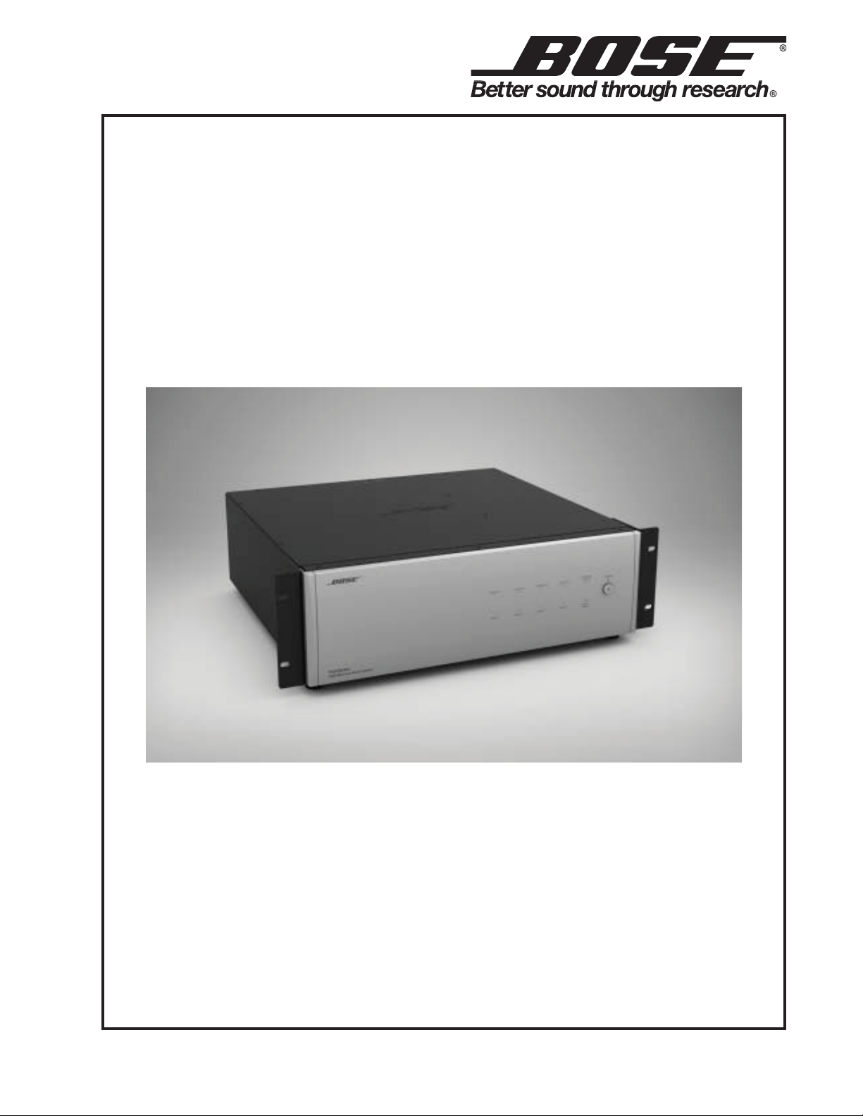
FreeSpace® 4400
Business Music System
©2008 Bose Corporation
Service Manual
Reference Number 294963-SM Rev. 00
Electronic Copy Only
Page 2

CONTENTS
Safety Information.............................................................................................................................3
Warranty.............................................................................................................................................4
Product Description..........................................................................................................................4
Specifications.............................................................................................................................. 5-10
Electrostatic Discharge Sensitive (ESDS) Device Handling .......................................................11
Part List Notes................................................................................................................................. 11
Product Variations ..........................................................................................................................11
Accessories .....................................................................................................................................12
Packaging Part List, FreeSpace
Figure 1. FreeSpace 4400 System Packaging View.........................................................................13
Packaging Part List, Rack Ear / Connector Kit ............................................................................14
Figure 2. Rack Ear / Connector Kit Packaging View ........................................................................ 14
Main Part List, FreeSpace Model 4400 Amplifier ................................................................... 15-16
Figure 3. FreeSp ace Model 4400 Business Music System Exploded View ......................................16
Electrical Part Lists................................................................................................................... 17-59
Front Panel PCB Assembly ...................................................................................................... 17-18
Digital Signal Processor PCB Assembly ................................................................................ 19-33
Digital Signal Processor Flash Memory PCB Assembly .............................................................33
Mic Sense PCB Assembly ........................................................................................................ 34-38
Power Supply / Power Amplifier PCB Assembly.................................................................... 39-56
Power Amplifier Driver PCB Assembly ................................................................................... 57-59
Disassembly Procedures ......................................................................................................... 60-62
Test Procedure Setup .....................................................................................................................63
Test Procedures ........................................................................................................................ 64-67
Troubleshooting........................................................................................................................ 68-75
Theory of Operation.................................................................................................................. 76-83
Microcontroller Code Update Procedure......................................................................................84
Circuit Board Layout Diagrams ............................................................................................... 85-93
Figure 4. Mic Sense PCB Top Etch Board Layout Diagram..............................................................85
Figure 5. Mic Sense PCB Bottom Etch Board Layout Diagram........................................................85
Figure 6. Flash Memory PCB Top Etch Board Layout Diagram........................................................85
Figure 7. Flash Memory PCB Bottom Etch Board Layout Diagram..................................................85
Figure 8. Wallplate Sense PCB Top Etch Board Layout Diagram ....................................................86
Figure 9. Wallplate Sense PCB Bottom Etch Board Layout Diagram...............................................86
Figure 10. AC Power Selector PCB Top Etch Board Layout Diagram ..............................................86
Figure 11. AC Power Selector PCB Bottom Etch Board Layout Diagram.........................................86
Figure 12. DSP PCB Top Etch Board Layout Diagram .....................................................................87
Figure 13. DSP PCB Bottom Etch Board Layout Diagram ...............................................................88
Figure 14. Front Panel PCB Top Etch Board Layout Diagram..........................................................89
Figure 15. Front Panel PCB Bottom Etch Board Layout Diagram ....................................................89
Figure 16. TriPath Module PCB Top Etch Board Layout Diagram ....................................................89
Figure 17. TriPath Module PCB Bottom Etch Board Layout Diagram ..............................................89
Figure 18. Amplifier Upper PCB Top Etch Board Layout Diagram....................................................90
Figure 19. Amplifier Upper PCB Bottom Etch Board Layout Diagram..............................................91
Figure 20. Amplifier/Power Supply Lower PCB Top Etch Board Layout Diagram.............................92
Figure 21. Amplifier/Power Supply Lower PCB Bottom Etch Board Layout Diagram.......................93
Integrated Circuit Diagrams................................................................................................... 94-105
Service Manual Revision History.................................................................................................106
®
4400 System ............................................................................13
2
Page 3

SAFETY INFORMATION
1. Parts that have special safety characteristics are identified by the symbol on schematics
or by special notes on the parts list. Use only replacement parts that have critical characteristics
recommended by the manufacturer.
2. Make leakage current or resistance measurements to determine that exposed parts are
acceptably insulated from the supply circuit before returning the unit to the customer.
Use the following checks to perform these measurements:
A. Leakage Current Hot Check-With the unit completely reassembled, plug the AC line cord
directly into a 120V AC outlet. (Do not use an isolation transformer during this test.) Use a
leakage current tester or a metering system that complies with American National Standards
Institute (ANSI) C101.1 "Leakage Current for Appliances" and Underwriters Laboratories (UL)
UL6500 / UL60065 / IEC 60065 paragraph 9.1.1. With the unit AC switch first in the ON position
and then in OFF position, measure from a known earth ground (metal waterpipe, conduit, etc.)
to all exposed metal parts of the unit (antennas, handle bracket, metal cabinet, screwheads,
metallic overlays, control shafts, etc.), especially any exposed metal parts that offer an electrical
return path to the chassis. Any current measured must not exceed 0.5 milliamp. Reverse the
unit power cord plug in the outlet and repeat test. ANY MEASUREMENTS NOT WITHIN THE
LIMITS SPECIFIED HEREIN INDICATE A POTENTIAL SHOCK HAZARD THAT MUST BE
ELIMINATED BEFORE RETURNING THE UNIT TO THE CUSTOMER.
B. Insulation Resistance Test Cold Check-(1) Unplug the power supply and connect a jumper
wire between the two prongs of the plug. (2) Turn on the power switch of the unit. (3) Measure
the resistance with an ohmmeter between the jumpered AC plug and each exposed metallic
cabinet part on the unit. When testing 3 wire products, the resistance measured to the product
enclosure should be between 2 and infinite MOhms. Also, the resistance measured to exposed
input/output connectors should be between 4 and infinite MOhms. When testing 2 wire products, the resistance measured to exposed input/output connectors should be between 4 and
infinite MOhms. If it is not within the limits specified, there is the possibility of a shock hazard,
and the unit must be repaired and rechecked before it is returned to the customer.
CAUTION
Danger of explosion if battery is incorrectly replaced.
Replace only with the same or equivalent type.
CAUTION: The Bose® FreeSpace® 4400 Business Music System
contains no user-serviceable parts. To prevent warranty infractions,
refer servicing to warranty service stations or factory service.
PROPRIETARY INFORMATION
THIS DOCUMENT CONTAINS PROPRIETARY INFORMATION OF
BOSE CORPORATION WHICH IS BEING FURNISHED ONLY FOR
THE PURPOSE OF SERVICING THE IDENTIFIED BOSE PRODUCT
BY AN AUTHORIZED BOSE SERVICE CENTER OR OWNER OF
THE BOSE PRODUCT, AND SHALL NOT BE REPRODUCED OR
USED FOR ANY OTHER PURPOSE.
3
Page 4

PRODUCT DESCRIPTION
FreeSpace® 4400 Business Music System
The Bose® FreeSpace 4400 Business Music System is an integrated four-channel digital signal
processor and 400-Watt power amplifier for 70/100V business music applications.
The FreeSpace 4400 chassis provides a total of four source inputs (two Line In, one Mic/Line
and one Mic/Line/Page) to meet the needs of most business music installations. A Music on
Hold (MOH) output is also provided for simple integration into a phone system.
As a single component, the chassis provides all of the processing and control features required
for one to four zone business music applications. These features include:
• Auto Volume: When used with the optional FreeSpace Auto Volume Sense Mic, the 4400
system dynamically controls the program level in each zone so that the audio program
material can always be heard, regardless of the background noise.
• Scheduling: Allows you to program the 4400 system for automated on/off and source
selections according to time of day or day of week.
• Opti-Voice
speech projection.
• Source Leveling: Automatically compensates for variations in source input levels.
• Dynamic Equalization: Maintains tonal balance at all listening levels.
• Room Equalization: Provides easy adjustment of tonal balance in each zone.
• Limiting: Protects loudspeakers from unwanted transient power loads.
• Signal Router: Meets the demands of most four-zone systems, allowing for any input signal
to be routed to any of the amplifier outputs.
• RS-232 Connection: Provides easy interfacing to your PC.
• Contact Closure Input: Allows remote power sequencing.
The integrated 400-Watt power amplifier features a patented power-sharing technology which
allocates power to each output.
For example, if you have a two-zone system that requires 5 Watts in zone 1 and 395 Watts in
zone 2, the FreeSpace 4400 system distributes the power based on those needs.
®
Paging: Provides the appropriate sound level regardless of variations in
The 4400 also includes an easy-to-replace memory module, which holds a design file and the
current hardware configuration.
WARRANTY
The Bose FreeSpace 4400 Business Music System is covered by a limited 5-year transferable
warranty.
4
Page 5

SPECIFICATIONS
Audio Input Source 1 Unbalanced RCA, shell grounded through a 301 Ohm resistor
Connectors: Source 2 Unbalanced RCA, shell grounded through a 301 Ohm resistor
Page Balanced 4 pin Beau style: +, -, ground and contact closure in
Aux/Mic/Line 3 pin Beau style, +, - and ground
Mic 1-4 3 pin Beau style, +, - and ground
Direct In 4 pin Beau style, +, -, ground, and contact closure in
Audio Output
Connectors: Line out 4 pin Beau style, +, -, ground, and contact closure in
MOH out 2 pin Beau style, + and Ground
Amp 1-4 2 pin, Beau style, + and -
Control Connectors: Remote 1-4 RJ-45, 8 pin, ground shell
Standby In 2 pin Beau style, contact closure in and ground
Dimensions: 5.25"H x 16.5"W x 15.5"D (13.3 x 43.8 x 39.4 cm)
Weight: Unpackaged: 30 lbs (13.6 kg)
Shipping: 41 lb (18.6 Kg)
AC Mains input: IEC standard User selectable 100/120 or 220/240V
3 pin 50/60 Hz
receptacle 300 Watts maximum
Overall Performance
Nominal Limits Conditions
Gain: 0 dB +1 dB At 1 kHz; input gain set to nominal 0 dB
Dynamic range: 100 dB >/= 96 dB Measured with ADC/DAC full scale mapped to
+17 dBV; this is THD +N measured at FS-60,
through A-weighting filter, and expressed in dB
below full scale
THD+N: .05% .1% At +10 Vrms output, for signal frequencies from
30 Hz to 20 kHz
Crosstalk at 1 kHz: -80 dB </= -70 dB Terminate unused input terminals with
100 Ohm balanced-connected resistors
Crosstalk at 10 kHz: -60 dB </= -50 dB Terminate unused input terminals with
100 Ohm balanced-connected resistors
Frequency response: 30 - 20 kHz +3 dB Reference 1 kHz, measured at 0 dBV input
Output noise: -70 dBV </= -65 dBV Channel noise measured through an
A -weighting filter. Gain structure set to deliver
rated power and expressed in dBV
5
Page 6

SPECIFICATIONS
Line Input Source 1 and 2
Nominal Limits Conditions
Source impedance: 200 Ohms 10 to 2k Ohm Frequency response specification maintained
with sources over this range
Input impedance
differential: +/> 50k Ohm +/-20% At 1 kHz
CMRR referred to 80 dB >/= 74 dB At 1 kHz, 20 dB gain, 200 Ohm source
output: impedance
Input sensitivity for -20 dBV to +/-1 dB At 1 kHz
codec FS: +17 dBV
Gain, all settings: 20 dB to +/-1 dB 1 kHz, 50 Ohm source
-20 dB
Maximum input level: +17 dBV >/= +17 dBV THD+N </= 0.3%, 30-20 kHz, 0 dB gain
THD+N: .001% .01% At +10 dBV output, 1 kHz, 20 dB gain
Crosstalk at 1 kHz: -90 dB </= -80 dB
Crosstalk at 10 kHz: -70 dB </= -60 dB
Frequency response: 30 to 20 kHz +/-1.5 dB Reference 1 kHz, measured at 20 dB gain
and with 0 dBV output
Page and Aux/Mic Inputs
Nominal Limits Conditions
Source impedance: 200 Ohms 10 to 2k Ohm Frequency response specification maintained
with sources over this range
Input impedance
differential: 20k Ohm +/-5% At 1 kHz
Equivalent input noise at 60 dB, at 60 dB, A-weighted RMS, 200 Ohm source
at INA129 gains of 60 -130 dBV -127 dBV termination
dB, 40 dB, 20 dB and at 40 dB, at 40 dB,
0 dB: -127 dBV -125 dBV
at 20 dB, at 20 dB,
-115 dBV -113 dBV
at 0 dB, at 0 dB,
-96 dBV -93 dBV
6
Page 7

SPECIFICATIONS
Page and Aux/Mic Inputs (continued)
Nominal Limits Conditions
CMRR referred 90 dB >/= 70 dB At 1 kHz, 60 dB gain, from source of nominal
to output: 200 Ohms
Input sensitivity for -60 dBV to +/-1 dB At 1 kHz
codec FS: +17 dBV
Gain, all settings: 20 dB to +/-1 dB 1 kHz, 50 Ohm source
-20 dB
Maximum input level: +17 dBV >/= 10 dBV THD+N </= 0.3%, 20-20 kHz, 0 dB gain
THD+N: .001% .01% At +10 dBV output, 1 kHz, 60 dB gain
Crosstalk at 1 kHz: -90 dB </= -80 dB
Crosstalk at 10 kHz: -70 dB </= -60 dB
Frequency response: 30 Hz to +0/-0.5 dB Reference 1 kHz, measured at 60 dB gain and
20 kHz with 0 dBV output
Sense Mic inputs
Nominal Limits Conditions
Source impedance: 200 Ohms 10 to 2k Ohm Frequency response specification maintained
with sources over this range
Input impedance
differential: 20k Ohm +5% At 1 kHz
Equivalent input noise at 60 dB, at 60 dB, A weighted RMS, 200 Ohm source termination
at INA129 gains of 60 -127 dBV -125 dBV
dB, 40 dB and 20 dB: at 40 dB, at 40 dB,
-115 dBV -112 dBV
at 20 dB, at 20 dB,
-96 dBV -93 dBV
CMRR referred
to output: 90 dB >/= 60 dB At 1 kHz, 60 dB gain, from source of nominal
200 Ohm
Phantom power: +12V +/-1V Open circuit
Input sensitivity for -60 dBV to +/-1 dB At 1 kHz
codec FS: +20 dBV
Gain, all settings: -60 dB to +/-1 dB 1 kHz, 50 Ohm source
+20 dB
7
Page 8

SPECIFICATIONS
Sense Mic inputs (continued)
Nominal Limits Conditions
Maximum input level: +10 dBV >/= 7 dBV THD+N </= 0.3%, 20-20 kHz, 0 dB gain
THD+N: -84 dB </= -80 dB At +10 dBV output, 1 kHz, 60 dB gain
Crosstalk at 1 kHz: -90 dB </= -80 dB
Crossalk at 10 kHz: -70 dB </= -60 dB
Frequency response: 20 Hz to +0/-0.5 dB Reference 1 kHz, measured at 60 dB
gain and 20 kHz with 0 dBV output
Direct Input
Nominal Limits Conditions
Source impedance: 200 Ohms 10 to 2k Ohm Frequency response specification maintained
with sources over this range
Input impedance
differential: +/> 10kOhms +/-20% At 1 kHz
CMRR referred
to output: 92 dB >/= 60 dB At 1 kHz, 20 dB gain, 200 Ohm source
impedance
Input sensitivity -20 dBV to +/-1 dB At 1 kHz
for codec FS: +17 dBV
Gain: 0 dB +/-1 dB From input connector to amplifier input stage
Maximum input level: +17 dBV >/= +17 dBV THD+N </= 0.3%, 30-20 kHz, 0 dB gain
THD+N: .001% .01% At +10 dBV output, 1 kHz, 20 dB gain
Crosstalk at 1 kHz: -90 dB </= -80 dB
Crosstalk at 10 kHz: -70 dB </= -60 dB
Frequency response: 30 Hz to +0/-0.5 dB Reference 1 kHz, measured at 20 dB gain and
20 kHz with 0 dBV output
Line Outputs
Nominal Limits Conditions
Output impedance: 200 Ohms +/-1% Impedance at 1 kHz, each output
terminal
Maximum output level: +17 dBV >/= +17 dBV 1 kHz, THD less than 0.1%, load 10 k Ohm,
differential
8
Page 9

SPECIFICATIONS
Line Outputs (continued)
Nominal Limits Conditions
CMRR referred
to output: 92 dB >/= 60 dB At 1 kHz, 20 dB gain, 200 Ohm source
impedance
Output noise: -90 dBV </= -85 dBV A-weighted, set for 0 dB gain
THD+N: .001% .01% At +10 dBV output, 1 kHz, 20 dB gain
Crosstalk at 1 kHz: -90 dB </= -80 dB Set for 0 dB gain, no limiting, terminate the
unused input with a 50 Ohm resistor
Crosstalk at 10 kHz: -70 dB </= -60 dB
Frequency response: 30 Hz to +0/-1.0 dB Reference 1 kHz, measured at 20 dB gain and
20 kHz with 0 dBV output
Turn on/off pop: 10 mV peak </= 50 mVpk As monitored by a listener, must be inaudible at
full gain using a Model 32 loudspeaker tapped
at 32W, with the unit set for no EQ and the
loudspeaker 3 feet from listener
Music on Hold (MOH)
Nominal Limits Conditions
Output impedance: 400 Ohms +/-1% Impedance at 1 kHz
Maximum output level: +17 dBV >/= +17 dBV 1 kHz, THD less than 0.1%, load 10k Ohm,
differential
Output noise: -90 dBV </= -85 dBV A-weighted, set for 0 dB gain
THD+N: .001% .01% At +17 dBV output, 1 kHz, 0 dB gain
Crosstalk at 1 kHz: -90 dB </= -80 dB Set for 0 dB gain, no limiting, terminate the
unused input with a 50 Ohm resistor
Crosstalk at 10 kHz: -70 dB </= -60 dB
Frequency response: 20 Hz to +0/-1.0 dB Reference 1 kHz, measured at 0 dB gain and
15 kHz with 0 dB output
Turn on/off pop: 10 mV peak </= 50 mVpk As monitored by a listener, must be inaudible at
full gain using a Model 32 loudspeaker tapped
at 32W, with the unit set for no EQ and the
loudspeaker 3 feet from listener
9
Page 10

SPECIFICATIONS
Power Amplifier
Nominal Limits Conditions
Power bandwidth: 30 Hz to 1% THD Loaded at 25 Ohms
20 kHz
Frequency response: 30 Hz to +/-3 dB Output voltage of 10 Vrms over a load
20 kHz impedance of 12.5 Ohms to 1000 Ohms
THD+N at 70.7 Vrms, .05% .1% 30 Hz to 20 kHz, 25 Ohm load, A weighted
200W:
THD+N at 70.7 Vrms, .5% 1 % 7 kHz, 12.5 Ohm load, A weighted
400W:
THD+N at 100 Vrms, .05% .1% 30 Hz to 20 kHz, 25 Ohm load, A weighted
200W:
THD+N at 100 Vrms, .5% 1% 7 kHz, 12.5 Ohm load, A weighted
400W:
Sensitivity at 70V: 11 dBV +/-1 dBV
Sensitivity at 100V: 14 dBV +/-1 dBV
Gain: 26 dB +/-0.5 dB
Output noise: -70 dBV -65 dBV A-weighted with a 20 kHz filter
Crosstalk at 1 kHz: -90 dB </= -80 dB Set for 0 dB gain, no limiting, terminate the
unused input with a 50 Ohm resistor
Crosstalk at 10 kHz: -70 dB </= -60 dB
Turn on/off pop: 10 mV peak </= 50 mVpk As monitored by a listener, must be inaudible at
full gain using a Model 32 loudspeaker tapped
at 32W, with the unit set for no EQ and the
loudspeaker 3 feet from listener
10
Page 11
ELECTROSTATIC DISCHARGE SENSITIVE (ESDS)
Description Bose® Product Code
DEVICE HANDLING
This unit contains ESDS devices. We recommend the following precautions when repairing,
replacing or transporting ESDS devices:
• Perform work at an electrically grounded work station.
• Wear wrist straps that connect to the station or heel straps that connect to conductive
floor mats.
• Avoid touching the leads or contacts of ESDS devices or PC boards even if properly
grounded. Handle boards by the edges only.
• Transport or store ESDS devices in ESD protective bags, bins, or totes. Do not insert
unprotected devices into materials such as plastic, polystyrene foam, clear plastic bags,
bubble wrap or plastic trays.
PART LIST NOTES
1. This part is not normally available from Customer Service. Approval from the Field Service
Manager is required before ordering.
2. The individual parts located on the PCBs are listed in the Electrical Part List.
3. This part is critical for safety purposes. Failure to use a substitute replacement with the
same safety characteristics as the recommended replacement part might create shock, fire
and/or other hazards.
4. This part is referenced for informational purposes only. It is not stocked as a repair part. Refer
to the next higher assembly for a replacement part.
PRODUCT VARIATIONS
FREESPACE® 4400 AMPLIFIER, 120V, US/CAN
FREESPACE 4400 AMPLIFIER, 230V, EURO
FREESPACE 4400 AMPLIFIER, 100V, JAPAN
FREESPACE 4400 AMPLIFIER, 230V, UK
FREESPACE 4400 AMPLIFIER, 240V, AUS
042346
042347
042348
042349
042350
11
Page 12
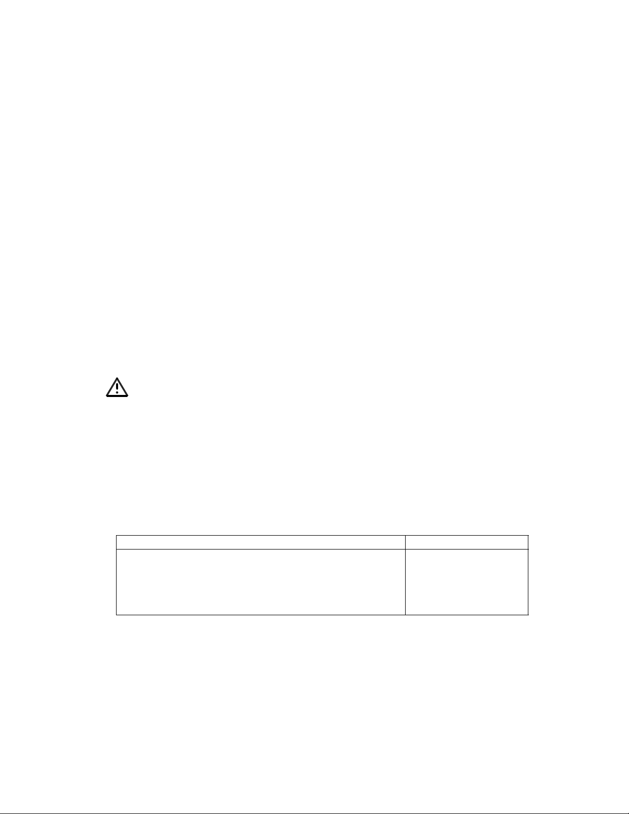
ACCESSORIES
Optional Bose® accessories for the FreeSpace® 4400 system are available.
• FreeSpace 4400 System AVM 1-Zone
User Interface (PC 042351) A wall-mountable keypad that fits into a standard doublegang junction box. It provides buttons for
volume up/down control, 1-3 source selection, and mute or Auto Vol-ume on/off controls for a single zone.
• FreeSpace 4400 System AVM 2-Zone
User Interface (PC 042352) A wall-mountable keypad that fits into a standard doublegang junction box. It provides buttons for
volume up/down control, 1-3 source selection, and mute or Auto Volume on/off controls for two zones.
FreeSpace
Select LINE 1
input source
Select LINE 2
input source
Select MIC/
LINE 3 input
source
FreeSpace
Select LINE 1
input source
Select LINE 2
input source
Select MIC/
LINE 3 input
source
®
AVM 1-Zone User Interface
MUTE /
AUTO VOL
®
AVM 2-Zone User Interface
SOURCE VOLUME SOURCE VOLUME
MUTE /
AUTO VO L
MUTE /
AUTO VO L
Volume up
(2 dB steps)
Volume down
(2 dB steps)
Mute
or
Auto volume
on/off
Volume up
(2 dB steps)
Volume down
(2 dB steps)
Mute
or
Auto volume
on/off
• FreeSpace 4400 System Page User
Interface (PC 042353) A wall-mount able
keypad that fits into a standard double-gang
junction box. It provides buttons for 1-4 page
zone selection, all page zones selection and
initiate page.
• FreeSpace 4400 System Auto Volume
Mic Kit (U.S.) (PC 042354) One sensing
microphone that can be mounted as is or in
a standard U.S. single-gang junction box.
• FreeSpace 4400 System Auto Volume
Mic Kit (Euro) (PC 042355) One sensing
microphone that can be mounted as is or in
a standard Euro single-gang junction box.
Zone A
controls
Page User Interface
Select paging
zone #1
Select paging
zone #3
Select all
paging zones
FreeSpace® 4400 System Auto Volume Mic Kit
[PC042354 (U.S.), PC042355 (Euro)]
Wall plate-microphone
assembly
Zone B
controls
Paint plug
(2) #6-32 (3 mm) screws
Select paging
zone #2
Select paging
zone #4
Initiate a page
(2) Wire nuts
12
Page 13
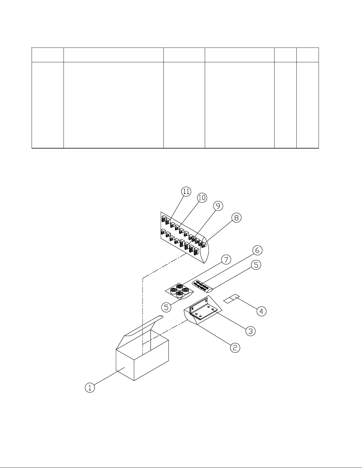
PACKAGING PART LIST
Item
Description Bose® Part
Vendor Part
Qty. Note
FreeSpace® 4400 System Packaging View (see Figure 1)
Number
1 CARTON 301388 1437-9101+1-3 1
2 PE FOAM HOLDER 301390 1493- 162 1+0 2
3 ACCESSORY KIT, INCLUDES:
CARTON
BRACKET, RACK EAR
POLYBAG, 04x5x9’
POLYBAG, 04x5x6’
SCREW, MACHINE, FLAT-CS
FOOT, RUBBER
LABEL, VOLTAGE SELE CT
2-TERMINAL I NPU T CONN
3-TERMINAL I NPU T CONN
4-TERMINAL I NPU T CONN
2-TERMINAL OUTPUT CONN
4 AC POWER CORD, 120V, US/CA N
AC POWER CORD, 230V , EURO
AC POWER CORD, 100V , JAPAN
AC POWER CORD, 230V , UK
AC POWER CORD, 240V , AUS
5 POLY BAG, 10x14’ - 1497-4122+0 1 4
6 DOCUMENT PACK, INCLUDES:
MANUAL
POLYBAG FOR MANUAL
FS 4400 SOFTWARE CD
QUICKSTART GUIDE
7 POLYBAG FOR UNIT - 1497-8012+0 1 4
8 FREESPACE 4400 AMPLIFIER REF - 1
Number
302389
-
-
-
298706
298707
170206
172930-02
172930-03
172930-04
260621-02
298165
298166
298167
298168
298169
302390
301433
-
301428-001
301434
Number
SVC-EXPO11+KIT
1481-0500+0
4135-6501+0
1497-1932+0
1497-2402+0
2901-4012+3000
4157-1121+0
3001-1631+0
2113-3252+0
2113-3143+0
2113-3147+0
2113-3258+0
7012-7340+0
7012-6980+0
7012-5530+0
7012-6603+0
7012-5430+1
SVC-EXPO11+DOC
4301-7264+0
1497-1062+0
4115-0005+0
3050-4011+0
1
1
2
1
1
8
4
2
7
2
4
5
1
1
1
1
1
1
1
1
1
4
4
4
4
3
3
3
4
Figure 1. FreeSpace 4400 System Packaging View
13
Page 14
PACKAGING PART LIST
Item
Description Bose® Part
Vendor Part Number Qty. Note
Rack Ear / Connector Kit (see Figure 2)
Number
- ACCESSORY KIT, INCLUDES: 302389 SVC-EXPO11+KIT 1
1 CARTON - 1481-0500+0 1 4
2 POLYBAG, 04x5x9’ - 1497-1932+0 1 4
3 BRACKET, RACK EAR - 4135-6501+0 2 4
4 LABEL, VOLTAGE SELECT 170206 3001-1631+0 2
5 POLY BAG, 04x5x6 - 1497-2402+0 1 4
6 SCREW, MACHINE, FLAT-CS 298706 2901-4012+3000 8
7 FOOT, RUBBER 298707 4157-1121+0 4
8 2-TERMINAL OUTPUT CONN 260621-02 2113-3258+0 5
9 4-TERMINAL INPUT CONN 172930-04 2113-3147+0 4
10 2-TERMINAL INPUT CONN 172930-02 2113-3252 + 0 7
11 3-TERMINAL INPUT CONN 172930-03 2113-3143+0 2
Number
Figure 2. Rack Ear / Connector Kit Packaging View
14
Page 15
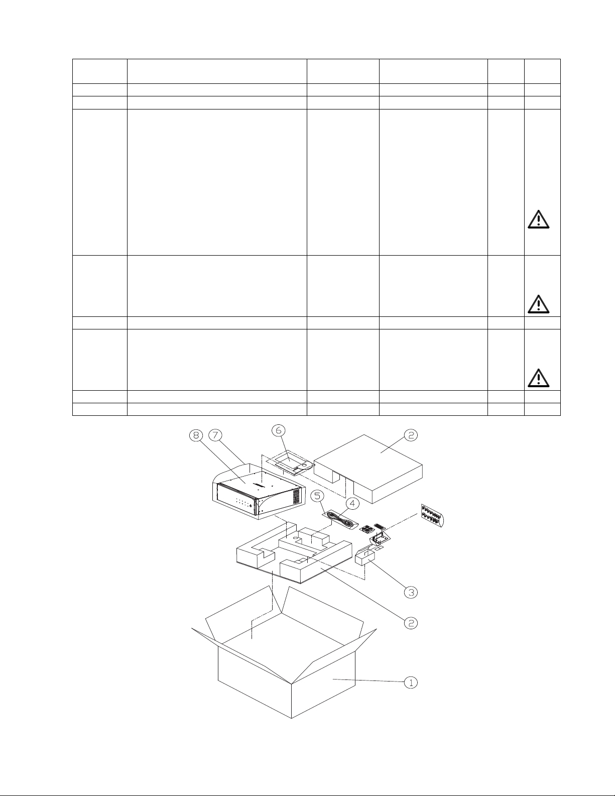
MAIN PART LIST
Item
Description Bose® Part
Vendor Part Number Qty. Note
FreeSp ace® Model 4400 Amplifier (see Figure 3)
Number
1 CHASSIS - 1406-0301+0 1 3, 4
2 SCREW, SELF TAPPING - 2941-3006+3000 14 4
3 SCREW, PAN, VOLT S EL CVR - 2900-3006+3200 2 4
4 COVER, AC SELECT SWITCH - 1467-7201+0 1 4
5 SWITCH, AC POWER, 2P1T 301394 5200-4881+0 1 3
6 SCREW, S-TITE, PL AT-CS - 2941-3012+3000 2
7 AC INLET, IEC 301396 2113-3050+0 1 3
8 FUSE HOLDER 301395 4153-1100+0 1 3
9 NUT, M4, BLK - 2640-4030+0730 2 4
10 EXTERNAL TOOTH WASHER - 2605-4008+0850 2 4
11 BRACKET, PLASTIC CLIP - 4155-2541+0 1 4
12 AC VOLTAGE SEL PCB AS SY 301397 SVC-EXPO01+P SP A1 1 2, 3
13 SCREW, S-TITE, PLAT-CS - 2941-3008+3000 6 4
14 TRANSFORMER, TOROIDAL,
AC
15 WASHER, M4x0.8x10 MM - 2600-8010+1602 1 4
16 SPRING WASHER - 2607-8020+1540 1 4
17 BOLT, FASTENER - 4135-7111+0 1 4
18 END CAP, F RO NT PANEL 301405 4155-2001+0 2
19 NUT, M3, NICK EL - 2640-3022+0544 4 4
20 LOCK WASHER, BLK - 2607-3008+0607 4 4
21 WASHER, METAL, NI C KEL - 2600-3008+1004 4 4
22 FAN, DC, 24V, 0 . 3A, 4200 RPM 304149 8913-0008+1 1 3
23 PANEL, FRO N T, ALUMINUM 301404 SVC-EXPO11+FPN 1
24 SCREW, SELF T AP PING - 2941-3006+3000 2 4
25 LENS, LED, 31 . 6x12.3x10 - 3717-3401+0 11 4
26 KNOB, PO WER ON/OFF 301408 2445-2801+0 1
27 PCB SUPPORT, 12 MM HIGH - 4152-0911+0 4 4
28 SCREW, SELF T AP PING - 2941-3006+3000 12 4
29 LED HOLDER - 4172-0030+0 11 4
30 LED PCB ASSY 301402 SVC-EXPO01+LED 1 2
31 TOP COVER, CHASSIS 301407 1406-0601+0 1 3
32 S-TITE, BLK - 2944-3008+3000 1 4
33 POWER AMP PCB MOD ASSY 301391 SVC-EXPO01+AM P 1 2
Number
301393 1806-3954+0 1 3
15
Page 16
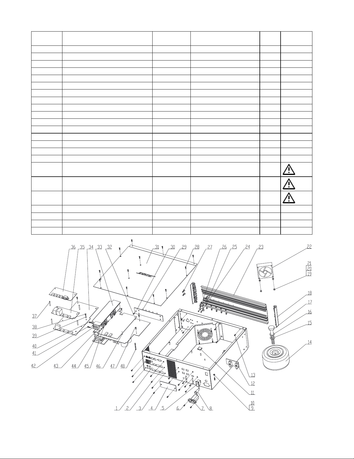
MAIN PART LIST
Item
Description Bose® Part
Vendor Part Number Qty. Note
FreeSp ace® Model 4400 Amplifier (continued) (see Figure 3)
Number
34 MAIN DSP PCB ASSY 301398 SVC-EXPO01+DSPJ 1 2
35 WALL PLATE PCB ASSY 301400 SVC-EXPO01+WALLP 1 2
36 MIC SENSE PC B ASSY 301399 SVC-EXPO01+MIC 1 2
37 BRACKET, BOTTOM - 4155-2411+0 4 4
38 S-TITE, BLK - 2944-3008+3000 2 4
39 LOCK WASHER, BLK - 2607-3008+0607 1 4
40 M3x20, BLK, ZN - 2904-3020+3000 4 4
41 SCREW, S-TI TE, PLAT-CS - 2941-3012+ 3000 10 4
42 HEATSINK, 220x124.2x70 MM
43 INSUL. SHT, 24x1 9x2 MM - 3100-7081+0 8 4
44 GND TERMINAL - 4135-6981+0 6 4
45 CLIP, HEATSINK - 4135-6511+0 4 4
46 POST, SUPPORT, PC B - 4155-2401+0 3 4
47 S-TITE, BLK - 2944-3008+3000 3 4
48 PILLAR, STANDOFF - 4135-7121+0 3 4
- FLASH MEMORY PCB ASSY 301401 SVC-EXPO01+FLASH 1 2
- SURGISTOR, 8A, 0.7 OHM,
N15SP2R5M
- FUSE, SLO-BLO, 6.30A,
100/110V (JAPAN, US/ C AN)
- FUSE, SLO-BLO, 3.15A,
230/240V (EURO, UK, AU S)
- HARN, 16P, DSP/REM OUT 301429 7012-7961+1 1
- HARN, 20P, DSP/MIC SENSE 301430 7012-7950+1 1
- HARN, 16P, DSP/UI 301431 7012-7960+1 1
- HARN, 34P, PS-PA/DSP 301432 7012-7970+0 1
Number
- 5400-9741+0 1 4
313000 5202-0027+0 1 3
177311-
06300
177311-
03150
5120-0040+0 1 3
5120-0079+0 1 3
®
Figure 3. FreeSpace
Model 4400 Business Music System Exploded View
16
Page 17
ELECTRICAL PART LIST
Reference
Description Vendor Part
Note
Reference
Description Vendor Part
Note
Front Panel PCB Assembly
Resistors
Designator
R101 1.1K, RMG, 0805, 1/10W, 1% 4720-112A+J 4
R102 10K, RMG, 0805, 1/10W, 1% 4720-103A+J 4
R107 10 OHM, RMG, 2512, 1W, 5% 4728-100J+3 4
R108 562 OHM, RMG, 0805, 1/10W, 1% 4720-5620+J 4
R109 562 OHM, RMG, 0805, 1/10W, 1% 4720-5620+J 4
R110 562 OHM, RMG, 0805, 1/10W, 1% 4720-5620+J 4
R111 562 OHM, RMG, 0805, 1/10W, 1% 4720-5620+J 4
R112 562 OHM, RMG, 0805, 1/10W, 1% 4720-5620+J 4
R113 562 OHM, RMG, 0805, 1/10W, 1% 4720-5620+J 4
R114 562 OHM, RMG, 0805, 1/10W, 1% 4720-5620+J 4
R115 562 OHM, RMG, 0805, 1/10W, 1% 4720-5620+J 4
R116 562 OHM, RMG, 0805, 1/10W, 1% 4720-5620+J 4
R117 562 OHM, RMG, 0805, 1/10W, 1% 4720-5620+J 4
R118 562 OHM, RMG, 0805, 1/10W, 1% 4720-5620+J 4
R119 562 OHM, RMG, 0805, 1/10W, 1% 4720-5620+J 4
R120 562 OHM, RMG, 0805, 1/10W, 1% 4720-5620+J 4
R121 562 OHM, RMG, 0805, 1/10W, 1% 4720-5620+J 4
R122 562 OHM, RMG, 0805, 1/10W, 1% 4720-5620+J 4
R123 562 OHM, RMG, 0805, 1/10W, 1% 4720-5620+J 4
R124 562 OHM, RMG, 0805, 1/10W, 1% 4720-5620+J 4
R125 562 OHM, RMG, 0805, 1/10W, 1% 4720-5620+J 4
R126 562 OHM, RMG, 0805, 1/10W, 1% 4720-5620+J 4
R127 562 OHM, RMG, 0805, 1/10W, 1% 4720-5620+J 4
R128 1.1K, RMG, 0805, 1/10W, 1% 4720-112A+J 4
R135 10K, RMG, 0805, 1/10W, 1% 4720-103A+J 4
R136 100K, RMG, 0805, 1/10W, 1% 4720-104A+J 4
Number
Capacitors
Designator
C101 0.1uF, CC, 0805, 25V, 10%, 1.2x2.0 150E-104K+J-BD 4
C102 0.1uF, CC, 0805, 25V, 10%, 1.2x2.0 150E-104K+J-BD 4
C103 0.1uF, CC, 0805, 25V, 10%, 1.2x2.0 150E-104K+J-BD 4
C104 0.1uF, CC, 0805, 25V, 10%, 1.2x2.0 150E-104K+J-BD 4
C105 0.1uF, CC, 0805, 25V, 10%, 1.2x2.0 150E-104K+J-BD 4
C106 10uF, CE, 25V, 20%, 5.3X5.4, SMD,
UWX1E100MCR1GB, NCC
C107 10uF, CE, 25V, 20%, 5.3X5.4, SMD,
C113 0.01uF, CC, 0805, 50V, 5% 150F-103J+J-BD 4
C114 0.1uF, CC, 0805, 25V, 10%, 1.2x2.0 150E-104K+J-BD 4
UWX1E100MCR1GB, NCC
Number
157E-106M+3-JJC 4
157E-106M+3-JJC 4
17
Page 18
ELECTRICAL PART LIST
Reference
Description Vendor Part
Note
Reference
Description Vendor Part
Note
Front Panel PCB Assembly
Diodes
Designator
D102 1N4148W, SOD-123, SMD, PANJIT 4801-48W0+3 4
D103 S1A, 1A, 50V, DO-214AA, SMD, PANJIT 480S-1A00+3 4
Designator
U101 SN74HC14D, SOP PACKAGE 3130-8680+0 4
U102 8 BIT SHIFT REG, M74HC595M1R, SO16, ST 3132-3591+0 4
U103 8 BIT SHIFT REG, M74HC595M1R, SO16, ST 3132-3591+0 4
U104 8 BIT SHIFT REG, M74HC595M1R, SO16, ST 3132-3591+0 4
U105 VOLT REG, SMD, POS, NJM78L05UA, SOT89 3132-3601+0 4
Integrated Circuits
Number
Number
18
Page 19
ELECTRICAL PART LIST
Reference
Description Vendor Part
Note
Digital Signal Processor PCB Assembly
Resistors
Designator
R501 18.2K, RMG, 1/10W, 1%, 0805 4720-1822+J 4
R502 182 OHM, RMG, 1/10W, 1%, 0805 4720-1820+J 4
R503 5.11K, RMG, 1/10W, 1%, 0805 4720-5111+J 4
R504 7.87K, RMG, 1/10W, 1%, 0805 4720-7871+J 4
R505 1.27K, RMG, 1/10W, 1%, 0805 4720-1271+J 4
R506 5.49K, RMG, 1/10W, 1%, 0805 4720-5491+J 4
R507 2K, RMG, 1/10W, 1%, 0805 4720-202A+J 4
R508 2K, RMG, 1/10W, 1%, 0805 4720-202A+J 4
R509 182 OHM, RMG, 1/10W, 1%, 0805 4720-1820+J 4
R510 100 OHM, RMG, 1/10W, 1%, 0805 4720-101A+J 4
R511 7.87K, RMG, 1/10W, 1%, 0805 4720-7871+J 4
R513 100K, RMG, 1/10W, 1%, 0805 4720-104A+J 4
R514 5.11K, RMG, 1/10W, 1%, 0805 4720-5111+J 4
R515 18.2K, RMG, 1/10W, 1%, 0805 4720-1822+J 4
R516 18.2K, RMG, 1/10W, 1%, 0805 4720-1822+J 4
R517 10 OHM, RMG, 1/10W, 1%, 0805 4720-100A+J 4
R518 182 OHM, RMG, 1/10W, 1%, 0805 4720-1820+J 4
R519 5.11K, RMG, 1/10W, 1%, 0805 4720-5111+J 4
R520 7.87K, RMG, 1/10W, 1%, 0805 4720-7871+J 4
R521 1.27K, RMG, 1/10W, 1%, 0805 4720-1271+J 4
R522 5.49K, RMG, 1/10W, 1%, 0805 4720-5491+J 4
R523 2K, RMG, 1/10W, 1%, 0805 4720-202A+J 4
R524 2K, RMG, 1/10W, 1%, 0805 4720-202A+J 4
R525 182 OHM, RMG, 1/10W, 1%, 0805 4720-1820+J 4
R526 7.87K, RMG, 1/10W, 1%, 0805 4720-7871+J 4
R528 100K, RMG, 1/10W, 1%, 0805 4720-104A+J 4
R529 5.11K, RMG, 1/10W, 1%, 0805 4720-5111+J 4
R530 18.2K, RMG, 1/10W, 1%, 0805 4720-1822+J 4
R531 18.2K, RMG, 1/10W, 1%, 0805 4720-1822+J 4
R532 5.11K, RMG, 1/10W, 1%, 0805 4720-5111+J 4
R533 7.87K, RMG, 1/10W, 1%, 0805 4720-7871+J 4
R534 5.11K, RMG, 1/10W, 1%, 0805 4720-5111+J 4
R537 2K, RMG, 1/10W, 1%, 0805 4720-202A+J 4
R538 2K, RMG, 1/10W, 1%, 0805 4720-202A+J 4
R539 100 OHM, RMG, 1/10W, 1%, 0805 4720-101A+J 4
R540 7.87K, RMG, 1/10W, 1%, 0805 4720-7871+J 4
R541 5.11K, RMG, 1/10W, 1%, 0805 4720-5111+J 4
R544 5.11K, RMG, 1/10W, 1%, 0805 4720-5111+J 4
R545 18.2K, RMG, 1/10W, 1%, 0805 4720-1822+J 4
R546 18.2K, RMG, 1/10W, 1%, 0805 4720-1822+J 4
R547 10 OHM, RMG, 1/10W, 1%, 0805 4720-100A+J 4
R548 5.11K, RMG, 1/10W, 1%, 0805 4720-5111+J 4
R549 7.87K, RMG, 1/10W, 1%, 0805 4720-7871+J 4
R550 5.11K, RMG, 1/10W, 1%, 0805 4720-5111+J 4
R553 2K, RMG, 1/10W, 1%, 0805 4720-202A+J 4
R554 2K, RMG, 1/10W, 1%, 0805 4720-202A+J 4
Number
19
Page 20

ELECTRICAL PART LIST
Reference
Description Vendor Part
Note
Digital Signal Processor PCB Assembly
Resistors (continued)
Designator
R555 7.87K, RMG, 1/10W, 1%, 0805 4720-7871+J 4
R556 5.11K, RMG, 1/10W, 1%, 0805 4720-5111+J 4
R557 5.11K, RMG, 1/10W, 1%, 0805 4720-5111+J 4
R558 18.2K, RMG, 1/10W, 1%, 0805 4720-1822+J 4
R561 4.75K, RMG, 1/10W, 1%, 0805 4720-4751+J 4
R562 5.9K, RMG, 1/10W, 1%, 0805 4720-592A+J 4
R563 1.1K, RMG, 1/10W, 1%, 0805 4720-112A+J 4
R566 100K, RMG, 1/10W, 1%, 0805 4720-104A+J 4
R568 25.5K, RMG, 1/10W, 1%, 0805 4720-2552+J 4
R571 100K, RMG, 1/10W, 1%, 0805 4720-104A+J 4
R572 10K, RMG, 1/10W, 1%, 0805 4720-103A+J 4
R573 25.5K, RMG, 1/10W, 1%, 0805 4720-2552+J 4
R575 100K, RMG, 1/10W, 1%, 0805 4720-104A+J 4
R576 10K, RMG, 1/10W, 1%, 0805 4720-103A+J 4
R577 25.5K, RMG, 1/10W, 1%, 0805 4720-2552+J 4
R579 100K, RMG, 1/10W, 1%, 0805 4720-104A+J 4
R580 10K, RMG, 1/10W, 1%, 0805 4720-103A+J 4
R581 1.91K, RMG, 1/10W, 1%, 0805 4720-1911+J 4
R582 25.5K, RMG, 1/10W, 1%, 0805 4720-2552+J 4
R583 10K, RMG, 1/10W, 1%, 0805 4720-103A+J 4
R584 4.75K, RMG, 1/10W, 1%, 0805 4720-4752+J 4
R585 301 OHM, RMG, 1/10W, 1%, 0805 4720-3010+J 4
R586 301 OHM, RMG, 1/10W, 1%, 0805 4720-3010+J 4
R587 301 OHM, RMG, 1/10W, 1%, 0805 4720-3010+J 4
R588 301 OHM, RMG, 1/10W, 1%, 0805 4720-3010+J 4
R589 10K, RMG, 1/10W, 1%, 0805 4720-103A+J 4
R590 26.7K, RMG, 1/10W, 1%, 0805 4720-2672+J 4
R591 301 OHM, RMG, 1/10W, 1%, 0805 4720-3010+J 4
R592 301 OHM, RMG, 1/10W, 1%, 0805 4720-3010+J 4
R593 301 OHM, RMG, 1/10W, 1%, 0805 4720-3010+J 4
R594 301 OHM, RMG, 1/10W, 1%, 0805 4720-3010+J 4
R599 10K, RMG, 1/10W, 1%, 0805 4720-103A+J 4
R600 10K, RMG, 1/10W, 1%, 0805 4720-103A+J 4
R601 10K, RMG, 1/10W, 1%, 0805 4720-103A+J 4
R603 49.9 OHM, RMG, 1/10W, 1%, 0805 4720-49R9+J 4
R604 49.9 OHM, RMG, 1/10W, 1%, 0805 4720-49R9+J 4
R605 10K, RMG, 1/10W, 1%, 0805 4720-103A+J 4
R608 10K, RMG, 1/10W, 1%, 0805 4720-103A+J 4
R609 100 OHM, RMG, 1/10W, 1%, 0805 4720-101A+J 4
R610 100 OHM, RMG, 1/10W, 1%, 0805 4720-101A+J 4
R611 100 OHM, RMG, 1/10W, 1%, 0805 4720-101A+J 4
R612 10K, RMG, 1/10W, 1%, 0805 4720-103A+J 4
R614 10K, RMG, 1/10W, 1%, 0805 4720-103A+J 4
R615 1K, RMG, 1/10W, 1%, 0805 4720-102A+J 4
R619 1K, RMG, 1/10W, 1%, 0805 4720-102A+J 4
R623 1K, RMG, 1/10W, 1%, 0805 4720-102A+J 4
Number
20
Page 21

ELECTRICAL PART LIST
Reference
Description Vendor Part
Note
Digital Signal Processor PCB Assembly
Resistors (continued)
Designator
R624 1M, RMG, 1/10W, 1%, 0805 4720-105A+J 4
R625 1M, RMG, 1/10W, 1%, 0805 4720-105A+J 4
R626 1M, RMG, 1/10W, 1%, 0805 4720-105A+J 4
R627 1M, RMG, 1/10W, 1%, 0805 4720-105A+J 4
R628 1K, RMG, 1/10W, 1%, 0805 4720-102A+J 4
R631 1K, RMG, 1/10W, 1%, 0805 4720-102A+J 4
R632 1K, RMG, 1/10W, 1%, 0805 4720-102A+J 4
R635 10K, RMG, 1/10W, 1%, 0805 4720-103A+J 4
R636 1.1K, RMG, 1/10W, 1%, 0805 4720-112A+J 4
R637 1K, RMG, 1/10W, 1%, 0805 4720-102A+J 4
R638 681 OHM, RMG, 1/10W, 1%, 0805 4720-6810+J 4
R640 681 OHM, RMG, 1/10W, 1%, 0805 4720-6810+J 4
R641 1M, RMG, 1/10W, 1%, 0805 4720-105A+J 4
R642 1.1K, RMG, 1/10W, 1%, 0805 4720-112A+J 4
R643 1K, RMG, 1/10W, 1%, 0805 4720-102A+J 4
R647 1.1K, RMG, 1/10W, 1%, 0805 4720-112A+J 4
R648 1K, RMG, 1/10W, 1%, 0805 4720-102A+J 4
R649 681 OHM, RMG, 1/10W, 1%, 0805 4720-6810+J 4
R651 681 OHM, RMG, 1/10W, 1%, 0805 4720-6810+J 4
R652 1M, RMG, 1/10W, 1%, 0805 4720-105A+J 4
R653 1.1K, RMG, 1/10W, 1%, 0805 4720-112A+J 4
R654 1K, RMG, 1/10W, 1%, 0805 4720-102A+J 4
R658 22.6K, RMG, 1/10W, 1%, 0805 4720-2262+J 4
R659 22.6K, RMG, 1/10W, 1%, 0805 4720-2262+J 4
R660 5.49K, RMG, 1/10W, 1%, 0805 4720-5491+J 4
R661 5.49K, RMG, 1/10W, 1%, 0805 4720-5491+J 4
R662 1.62K, RMG, 1/10W, 1%, 0805 4720-1621+J 4
R663 1.62K, RMG, 1/10W, 1%, 0805 4720-1621+J 4
R664 499 OHM, RMG, 1/10W, 1%, 0805 4720-4990+J 4
R665 499 OHM, RMG, 1/10W, 1%, 0805 4720-4990+J 4
R666 150 OHM, RMG, 1/10W, 1%, 0805 4720-151A+J 4
R667 150 OHM, RMG, 1/10W, 1%, 0805 4720-151A+J 4
R668 49.9 OHM, RMG, 1/10W, 1%, 0805 4720-49R9+J 4
R669 49.9 OHM, RMG, 1/10W, 1%, 0805 4720-49R9+J 4
R670 499 OHM, RMG, 1/10W, 1%, 0805 4720-4990+J 4
R671 5.49K, RMG, 1/10W, 1%, 0805 4720-5491+J 4
R672 4.12K, RMG, 1/10W, 1%, 0805 4720-4121+J 4
R673 16 OHM, RMG, 1W, 5%, 2512 4728-160J+3 4
R674 2.2 OHM, RMG, 1W, 5%, 2512 4728-2R2J+3 4
R675 16 OHM, RMG, 1W, 5%, 2512 4728-160J+3 4
R677 10 OHM, RMG, 1W, 5%, 2512 4728-100J+3 4
R678 10 OHM, RMG, 1W, 5%, 2512 4728-100J+3 4
R679 10 OHM, RMG, 1W, 5%, 2512 4728-100J+3 4
R680 10K, RMG, 1/10W, 1%, 0805 4720-103A+J 4
R681 2K, RMG, 1/10W, 1%, 0805 4720-202A+J 4
R682 562 OHM, RMG, 1/10W, 1%, 0805 4720-5620+J 4
Number
21
Page 22

ELECTRICAL PART LIST
Reference
Description Vendor Part
Note
Digital Signal Processor PCB Assembly
Resistors (continued)
Designator
R683 2K, RMG, 1/10W, 1%, 0805 4720-202A+J 4
R684 100K, RMG, 1/10W, 1%, 0805 4720-104A+J 4
R685 100K, RMG, 1/10W, 1%, 0805 4720-104A+J 4
R686 100K, RMG, 1/10W, 1%, 0805 4720-104A+J 4
R687 2K, RMG, 1/10W, 1%, 0805 4720-202A+J 4
R688 5.49K, RMG, 1/10W, 1%, 0805 4720-5491+J 4
R689 2.49K, RMG, 1/10W, 1%, 0805 4720-2491+J 4
R690 3.09K, RMG, 1/10W, 1%, 0805 4720-3091+J 4
R691 1.1K, RMG, 1/10W, 1%, 0805 4720-112A+J 4
R692 1.1K, RMG, 1/10W, 1%, 0805 4720-112A+J 4
R693 1.1K, RMG, 1/10W, 1%, 0805 4720-112A+J 4
R694 1.1K, RMG, 1/10W, 1%, 0805 4720-112A+J 4
R698 1.1K, RMG, 1/10W, 1%, 0805 4720-112A+J 4
R699 5.49K, RMG, 1/10W, 1%, 0805 4720-5491+J 4
R700 33.2K, RMG, 1/10W, 1%, 0805 4720-3322+J 4
R701 9.09K, RMG, 1/10W, 1%, 0805 4720-9091+J 4
R702 15K, RMG, 1/10W, 1%, 0805 4720-153A+J 4
R703 20K, RMG, 1/10W, 1%, 0805 4720-203A+J 4
R704 22.1K, RMG, 1/10W, 1%, 0805 4720-2212+J 4
R705 30.1K, RMG, 1/10W, 1%, 0805 4720-3012+J 4
R706 49.9K, RMG, 1/10W, 1%, 0805 4720-4992+J 4
R707 10K, RMG, 1/10W, 1%, 0805 4720-103A+J 4
R708 43.2K, RMG, 1/10W, 1%, 0805 4720-4322+J 4
R709 11K, RMG, 1/10W, 1%, 0805 4720-113A+J 4
R710 49.9K, RMG, 1/10W, 1%, 0805 4720-4992+J 4
R711 15K, RMG, 1/10W, 1%, 0805 4720-153A+J 4
R712 22.1K, RMG, 1/10W, 1%, 0805 4720-2212+J 4
R715 20K, RMG, 1/10W, 1%, 0805 4720-203A+J 4
R716 22.1K, RMG, 1/10W, 1%, 0805 4720-2212+J 4
R717 30.1K, RMG, 1/10W, 1%, 0805 4720-3012+J 4
R718 49.9K, RMG, 1/10W, 1%, 0805 4720-4992+J 4
R719 10K, RMG, 1/10W, 1%, 0805 4720-103A+J 4
R720 43.2K, RMG, 1/10W, 1%, 0805 4720-4322+J 4
R721 11K, RMG, 1/10W, 1%, 0805 4720-113A+J 4
R722 49.9K, RMG, 1/10W, 1%, 0805 4720-4992+J 4
R723 15K, RMG, 1/10W, 1%, 0805 4720-153A+J 4
R724 15K, RMG, 1/10W, 1%, 0805 4720-153A+J 4
R725 22.1K, RMG, 1/10W, 1%, 0805 4720-2212+J 4
R728 33.2K, RMG, 1/10W, 1%, 0805 4720-3322+J 4
R729 9.09K, RMG, 1/10W, 1%, 0805 4720-9091+J 4
R730 20K, RMG, 1/10W, 1%, 0805 4720-203A+J 4
R731 22.1K, RMG, 1/10W, 1%, 0805 4720-2212+J 4
R732 30.1K, RMG, 1/10W, 1%, 0805 4720-3012+J 4
R733 49.9K, RMG, 1/10W, 1%, 0805 4720-4992+J 4
R734 10K, RMG, 1/10W, 1%, 0805 4720-103A+J 4
R735 43.2K, RMG, 1/10W, 1%, 0805 4720-4322+J 4
Number
22
Page 23

ELECTRICAL PART LIST
Reference
Description Vendor Part
Note
Digital Signal Processor PCB Assembly
Resistors (continued)
Designator
R736 11K, RMG, 1/10W, 1%, 0805 4720-113A+J 4
R737 49.9K, RMG, 1/10W, 1%, 0805 4720-4992+J 4
R738 15K, RMG, 1/10W, 1%, 0805 4720-153A+J 4
R739 15K, RMG, 1/10W, 1%, 0805 4720-153A+J 4
R740 22.1K, RMG, 1/10W, 1%, 0805 4720-2212+J 4
R743 33.2K, RMG, 1/10W, 1%, 0805 4720-3322+J 4
R744 9.09K, RMG, 1/10W, 1%, 0805 4720-9091+J 4
R745 20K, RMG, 1/10W, 1%, 0805 4720-203A+J 4
R746 22.1K, RMG, 1/10W, 1%, 0805 4720-2212+J 4
R747 30.1K, RMG, 1/10W, 1%, 0805 4720-3012+J 4
R748 49.9K, RMG, 1/10W, 1%, 0805 4720-4992+J 4
R749 10K, RMG, 1/10W, 1%, 0805 4720-103A+J 4
R750 43.2K, RMG, 1/10W, 1%, 0805 4720-4322+J 4
R751 11K, RMG, 1/10W, 1%, 0805 4720-113A+J 4
R752 49.9K, RMG, 1/10W, 1%, 0805 4720-4992+J 4
R753 15K, RMG, 1/10W, 1%, 0805 4720-153A+J 4
R754 15K, RMG, 1/10W, 1%, 0805 4720-153A+J 4
R755 22.1K, RMG, 1/10W, 1%, 0805 4720-2212+J 4
R758 33.2K, RMG, 1/10W, 1%, 0805 4720-3322+J 4
R759 9.09K, RMG, 1/10W, 1%, 0805 4720-9091+J 4
R760 10K, RMG, 1/10W, 1%, 0805 4720-103A+J 4
R761 1.1K, RMG, 1/10W, 1%, 0805 4720-112A+J 4
R762 24.9K, RMG, 1/10W, 1%, 0805 4720-2492+J 4
R763 4.99K, RMG, 1/10W, 1%, 0805 4720-4991+J 4
R764 3.09K, RMG, 1/10W, 1%, 0805 4720-3091+J 4
R765 2K, RMG, 1/10W, 1%, 0805 4720-202A+J 4
R766 2K, RMG, 1/10W, 1%, 0805 4720-202A+J 4
R771 0 OHM, RMG, 1/10W, 5%, 0805 4720-000J+J 4
R772 0 OHM, RMG, 1/10W, 5%, 0805 4720-000J+J 4
R773 0 OHM, RMG, 1/10W, 5%, 0805 4720-000J+J 4
R774 0 OHM, RMG, 1/10W, 5%, 0805 4720-000J+J 4
R778 100 OHM, RMG, 1/10W, 1%, 0805 4720-101A+J 4
R779 100 OHM, RMG, 1/10W, 1%, 0805 4720-101A+J 4
R780 100 OHM, RMG, 1/10W, 1%, 0805 4720-101A+J 4
R781 100 OHM, RMG, 1/10W, 1%, 0805 4720-101A+J 4
R782 100 OHM, RMG, 1/10W, 1%, 0805 4720-101A+J 4
R783 1.1K, RMG, 1/10W, 1%, 0805 4720-112A+J 4
R784 1.1K, RMG, 1/10W, 1%, 0805 4720-112A+J 4
R785 3.09K, RMG, 1/10W, 1%, 0805 4720-3091+J 4
R786 20K, RMG, 1/10W, 1%, 0805 4720-203A+J 4
R787 1.1K, RMG, 1/10W, 1%, 0805 4720-112A+J 4
R788 301 OHM, RMG, 1/10W, 1%, 0805 4720-3010+J 4
R789 301 OHM, RMG, 1/10W, 1%, 0805 4720-3010+J 4
R790 0 OHM, RMG, 1/10W, 5%, 0805 4720-000J+J 4
R791 0 OHM, RMG, 1/10W, 5%, 0805 4720-000J+J 4
Number
23
Page 24
ELECTRICAL PART LIST
Reference
Description Vendor Part
Note
Reference
Description Vendor Part
Note
Digital Signal Processor PCB Assembly
Resistors (continued)
Designator
R792 100 OHM, RMG, 1/10W, 1%, 0805 4720-101A+J 4
R793 267 OHM, RMG, 1/10W, 1%, 0805 4720-2670+J 4
R794 10K, RMG, 1/10W, 1%, 0805 4720-103A+J 4
Designator
C501 68pF, CC, 50V, 5%, 0805, 1.25X2.0 150F-680J+J-BDM 4
C503 2200pF, CC, 50V, 10%, 0805, 1.2x2.0 150F-222K+J-BD 4
C504 470pF, CC, 50V, 5%, 0805, 1.2x2.0 150F-471J+J-BD 4
C505 68pF, CC, 50V, 5%, 0805, 1.25X2.0 150F-680J+J-BDM 4
C506 2.2uF, CE, 35V, 20%, SMD, 3X5.4,
UWX1V2R2MCR2GB, NCC
C507 0.1uF, CC, 25V, 10%, 0805, 1.2x2.0 150E-104K+J-BD 4
C508 10uF, CE, 25V, 20%, 5.3X5.4, SMD,
UWX1E100MCR1GB, NCC
C509 68pF, CC, 50V, 5%, 0805, 1.25X2.0 150F-680J+J-BDM 4
C510 0.1uF, CC, 25V, 10%, 0805, 1.2x2.0 150E-104K+J-BD 4
C511 0.1uF, CC, 25V, 10%, 0805, 1.2x2.0 150E-104K+J-BD 4
C513 2200pF, CC, 50V, 10%, 0805, 1.2x2.0 150F-222K+J-BD 4
C514 470pF, CC, 50V, 5%, 0805, 1.2x2.0 150F-471J+J-BD 4
C515 68pF, CC, 50V, 5%, 0805, 1.25X2.0 150F-680J+J-BDM 4
C516 2.2uF, CE, 35V, 20%, SMD, 3X5.4,
UWX1V2R2MCR2GB, NCC
C517 4.7uF, CE, 25V, 20%, SMD, 4X5.3 157E-475M+3-GJ 4
C518 0.1uF, CC, 25V, 10%, 0805, 1.2x2.0 150E-104K+J-BD 4
C519 68pF, CC, 50V, 5%, 0805, 1.25X2.0 150F-680J+J-BDM 4
C521 2200pF, CC, 50V, 10%, 0805, 1.2x2.0 150F-222K+J-BD 4
C522 470pF, CC, 50V, 5%, 0805, 1.2x2.0 150F-471J+J-BD 4
C523 68pF, CC, 50V, 5%, 0805, 1.25X2.0 150F-680J+J-BDM 4
C525 0.1uF, CC, 25V, 10%, 0805, 1.2x2.0 150E-104K+J-BD 4
C526 10uF, CE, 25V, 20%, 5.3X5.4, SMD,
UWX1E100MCR1GB, NCC
C527 68pF, CC, 50V, 5%, 0805, 1.25X2.0 150F-680J+J-BDM 4
C528 0.1uF, CC, 25V, 10%, 0805, 1.2x2.0 150E-104K+J-BD 4
C529 0.1uF, CC, 25V, 10%, 0805, 1.2x2.0 150E-104K+J-BD 4
C531 470pF, CC, 50V, 5%, 0805, 1.2x2.0 150F-471J+J-BD 4
C532 2200pF, CC, 50V, 10%, 0805, 1.2x2.0 150F-222K+J-BD 4
C533 68pF, CC, 50V, 5%, 0805, 1.25X2.0 150F-680J+J-BDM 4
C534 4.7uF, CE, 25V, 20%, SMD, 4X5.3 157E-475M+3-GJ 4
C535 0.1uF, CC, 25V, 10%, 0805, 1.2x2.0 150E-104K+J-BD 4
C537 10uF, CE, 25V, 20%, 5.3X5.4, SMD,
UWX1E100MCR1GB, NCC
C538 0.1uF, CC, 25V, 10%, 0805, 1.2x2.0 150E-104K+J-BD 4
C539 0.1uF, CC, 25V, 10%, 0805, 1.2x2.0 150E-104K+J-BD 4
C541 0.1uF, CC, 25V, 10%, 0805, 1.2x2.0 150E-104K+J-BD 4
C542 0.1uF, CC, 25V, 10%, 0805, 1.2x2.0 150E-104K+J-BD 4
Capacitors
Number
Number
157Q-225M+3-EJC 4
157E-106M+3-JJC 4
157Q-225M+3-EJC 4
157E-106M+3-JJC 4
157E-106M+3-JJC 4
24
Page 25
ELECTRICAL PART LIST
Reference
Description Vendor Part
Note
Digital Signal Processor PCB Assembly
Capacitors (continued)
Designator
C545 0.1uF, CC, 25V, 10%, 0805, 1.2x2.0 150E-104K+J-BD 4
C547 0.1uF, CC, 25V, 10%, 0805, 1.2x2.0 150E-104K+J-BD 4
C548 0.1uF, CC, 25V, 10%, 0805, 1.2x2.0 150E-104K+J-BD 4
C551 1000pF, CC, 50V, 5%, 0805, 1.25X2.0 150F-102J+J-BDM 4
C552 68pF, CC, 50V, 5%, 0805, 1.25X2.0 150F-680J+J-BDM 4
C553 1000pF, CC, 50V, 5%, 0805, 1.25X2.0 150F-102J+J-BDM 4
C554 10uF, CE, 25V, 20%, 5.3X5.4, SMD,
C555 0.1uF, CC, 25V, 10%, 0805, 1.2x2.0 150E-104K+J-BD 4
C556 0.1uF, CC, 25V, 10%, 0805, 1.2x2.0 150E-104K+J-BD 4
C557 0.1uF, CC, 25V, 10%, 0805, 1.2x2.0 150E-104K+J-BD 4
C558 0.1uF, CC, 25V, 10%, 0805, 1.2x2.0 150E-104K+J-BD 4
C559 0.1uF, CC, 25V, 10%, 0805, 1.2x2.0 150E-104K+J-BD 4
C560 0.1uF, CC, 25V, 10%, 0805, 1.2x2.0 150E-104K+J-BD 4
C561 0.1uF, CC, 25V, 10%, 0805, 1.2x2.0 150E-104K+J-BD 4
C562 0.1uF, CC, 25V, 10%, 0805, 1.2x2.0 150E-104K+J-BD 4
C563 0.1uF, CC, 25V, 10%, 0805, 1.2x2.0 150E-104K+J-BD 4
C564 0.1uF, CC, 25V, 10%, 0805, 1.2x2.0 150E-104K+J-BD 4
C565 0.1uF, CC, 25V, 10%, 0805, 1.2x2.0 150E-104K+J-BD 4
C566 0.1uF, CC, 25V, 10%, 0805, 1.2x2.0 150E-104K+J-BD 4
C567 0.1uF, CC, 25V, 10%, 0805, 1.2x2.0 150E-104K+J-BD 4
C568 0.1uF, CC, 25V, 10%, 0805, 1.2x2.0 150E-104K+J-BD 4
C569 0.1uF, CC, 25V, 10%, 0805, 1.2x2.0 150E-104K+J-BD 4
C570 0.1uF, CC, 25V, 10%, 0805, 1.2x2.0 150E-104K+J-BD 4
C572 0.1uF, CC, 25V, 10%, 0805, 1.2x2.0 150E-104K+J-BD 4
C573 0.1uF, CC, 25V, 10%, 0805, 1.2x2.0 150E-104K+J-BD 4
C575 0.1uF, CC, 25V, 10%, 0805, 1.2x2.0 150E-104K+J-BD 4
C576 0.1uF, CC, 25V, 10%, 0805, 1.2x2.0 150E-104K+J-BD 4
C577 0.1uF, CC, 25V, 10%, 0805, 1.2x2.0 150E-104K+J-BD 4
C578 33pF, CC, 50V, 5%, 0805, 1.2x2 150F-330J+J-BD 4
C579 33pF, CC, 50V, 5%, 0805, 1.2x2 150F-330J+J-BD 4
C580 0.1uF, CC, 25V, 10%, 0805, 1.2x2.0 150E-104K+J-BD 4
C581 0.1uF, CC, 25V, 10%, 0805, 1.2x2.0 150E-104K+J-BD 4
C582 0.1uF, CC, 25V, 10%, 0805, 1.2x2.0 150E-104K+J-BD 4
C583 0.1uF, CC, 25V, 10%, 0805, 1.2x2.0 150E-104K+J-BD 4
C584 0.1uF, CC, 25V, 10%, 0805, 1.2x2.0 150E-104K+J-BD 4
C585 0.1uF, CC, 25V, 10%, 0805, 1.2x2.0 150E-104K+J-BD 4
C586 4700pF, CC, 50V, 5%, 0805, 1.2x2.0 150F-472J+J-BD 4
C587 0.1uF, CC, 25V, 10%, 0805, 1.2x2.0 150E-104K+J-BD 4
C588 0.1uF, CC, 25V, 10%, 0805, 1.2x2.0 150E-104K+J-BD 4
C591 1000pF, CC, 50V, 5%, 0805, 1.25X2.0 150F-102J+J-BDM 4
C592 2.2uF, CE, 35V, 20%, SMD, 3X5.4,
C593 100pF, CC, 50V, 5%, 0805, 1.2x2.0 150F-101J+J-BD 4
C595 2.2uF, CE, 35V, 20%, SMD, 3X5.4,
UWX1E100MCR1GB, NCC
UWX1V2R2MCR2GB, NCC
UWX1V2R2MCR2GB, NCC
Number
157E-106M+3-JJC 4
157Q-225M+3-EJC 4
157Q-225M+3-EJC 4
25
Page 26

ELECTRICAL PART LIST
Reference
Description Vendor Part
Note
Digital Signal Processor PCB Assembly
Capacitors (continued)
Designator
C597 1000pF, CC, 50V, 5%, 0805, 1.25X2.0 150F-102J+J-BDM 4
C598 2.2uF, CE, 35V, 20%, SMD, 3X5.4,
UWX1V2R2MCR2GB, NCC
C599 2.2uF, CE, 35V, 20%, SMD, 3X5.4,
UWX1V2R2MCR2GB, NCC
C601 1000pF, CC, 50V, 5%, 0805, 1.25X2.0 150F-102J+J-BDM 4
C602 0.1uF, CC, 25V, 10%, 0805, 1.2x2.0 150E-104K+J-BD 4
C603 0.1uF, CC, 25V, 10%, 0805, 1.2x2.0 150E-104K+J-BD 4
C604 100pF, CC, 50V, 5%, 0805, 1.2x2.0 150F-101J+J-BD 4
C607 1000pF, CC, 50V, 5%, 0805, 1.25X2.0 150F-102J+J-BDM 4
C609 0.1uF, CC, 25V, 10%, 0805, 1.2x2.0 150E-104K+J-BD 4
C612 0.1uF, CC, 25V, 10%, 0805, 1.2x2.0 150E-104K+J-BD 4
C613 0.1uF, CC, 25V, 10%, 0805, 1.2x2.0 150E-104K+J-BD 4
C614 0.1uF, CC, 25V, 10%, 0805, 1.2x2.0 150E-104K+J-BD 4
C617 0.1uF, CC, 25V, 10%, 0805, 1.2x2.0 150E-104K+J-BD 4
C618 0.1uF, CC, 25V, 10%, 0805, 1.2x2.0 150E-104K+J-BD 4
C619 0.1uF, CC, 25V, 10%, 0805, 1.2x2.0 150E-104K+J-BD 4
C622 0.1uF, CC, 25V, 10%, 0805, 1.2x2.0 150E-104K+J-BD 4
C623 0.1uF, CC, 25V, 10%, 0805, 1.2x2.0 150E-104K+J-BD 4
C624 0.1uF, CC, 25V, 10%, 0805, 1.2x2.0 150E-104K+J-BD 4
C625 0.1uF, CC, 25V, 10%, 0805, 1.2x2.0 150E-104K+J-BD 4
C626 330uF, CE, 25V, 20%, 8X10, SMD,
UUD1E331MCR1GB, NCC
C627 2200pF, CC, 50V, 10%, 0805, 1.2x2.0 150F-222K+J-BD 4
C628 100pF, CC, 50V, 5%, 0805, 1.2x2.0 150F-101J+J-BD 4
C629 0.1uF, CC, 25V, 10%, 0805, 1.2x2.0 150E-104K+J-BD 4
C630 330uF, CE, 25V, 20%, 8X10, SMD,
UUD1E331MCR1GB, NCC
C631 0.1uF, CC, 25V, 10%, 0805, 1.2x2.0 150E-104K+J-BD 4
C632 1000pF, CC, 50V, 5%, 0805, 1.25X2.0 150F-102J+J-BDM 4
C633 2200pF, CC, 50V, 10%, 0805, 1.2x2.0 150F-222K+J-BD 4
C634 0.1uF, CC, 25V, 10%, 0805, 1.2x2.0 150E-104K+J-BD 4
C635 0.1uF, CC, 25V, 10%, 0805, 1.2x2.0 150E-104K+J-BD 4
C636 0.1uF, CC, 25V, 10%, 0805, 1.2x2.0 150E-104K+J-BD 4
C637 0.1uF, CC, 25V, 10%, 0805, 1.2x2.0 150E-104K+J-BD 4
C638 330uF, CE, 25V, 20%, 8X10, SMD,
UUD1E331MCR1GB, NCC
C639 0.1uF, CC, 25V, 10%, 0805, 1.2x2.0 150E-104K+J-BD 4
C640 2200pF, CC, 50V, 10%, 0805, 1.2x2.0 150F-222K+J-BD 4
C641 100pF, CC, 50V, 5%, 0805, 1.2x2.0 150F-101J+J-BD 4
C642 0.1uF, CC, 25V, 10%, 0805, 1.2x2.0 150E-104K+J-BD 4
C643 0.1uF, CC, 25V, 10%, 0805, 1.2x2.0 150E-104K+J-BD 4
C644 330uF, CE, 25V, 20%, 8X10, SMD,
UUD1E331MCR1GB, NCC
C645 0.1uF, CC, 25V, 10%, 0805, 1.2x2.0 150E-104K+J-BD 4
C646 2200pF, CC, 50V, 10%, 0805, 1.2x2.0 150F-222K+J-BD 4
C647 0.1uF, CC, 25V, 10%, 0805, 1.2x2.0 150E-104K+J-BD 4
Number
157Q-225M+3-EJC 4
157Q-225M+3-EJC 4
157E-337M+3-OSC
157E-337M+3-OSC
157E-337M+3-OSC
157E-337M+3-OSC
4
4
4
4
26
Page 27
ELECTRICAL PART LIST
Reference
Description Vendor Part
Note
Digital Signal Processor PCB Assembly
Capacitors (continued)
Designator
C648 0.1uF, CC, 25V, 10%, 0805, 1.2x2.0 150E-104K+J-BD 4
C649 0.1uF, CC, 25V, 10%, 0805, 1.2x2.0 150E-104K+J-BD 4
C650 0.1uF, CC, 25V, 10%, 0805, 1.2x2.0 150E-104K+J-BD 4
C651 0.1uF, CC, 25V, 10%, 0805, 1.2x2.0 150E-104K+J-BD 4
C652 0.1uF, CC, 25V, 10%, 0805, 1.2x2.0 150E-104K+J-BD 4
C653 0.1uF, CC, 25V, 10%, 0805, 1.2x2.0 150E-104K+J-BD 4
C654 0.1uF, CC, 25V, 10%, 0805, 1.2x2.0 150E-104K+J-BD 4
C655 0.1uF, CC, 25V, 10%, 0805, 1.2x2.0 150E-104K+J-BD 4
C656 0.01uF, CC, 50V, 5%, 0805 150F-103J+J-BD 4
C657 0.01uF, CC, 50V, 5%, 0805 150F-103J+J-BD 4
C658 0.01uF, CC, 50V, 5%, 0805 150F-103J+J-BD 4
C659 0.01uF, CC, 50V, 5%, 0805 150F-103J+J-BD 4
C660 0.1uF, CC, 25V, 10%, 0805, 1.2x2.0 150E-104K+J-BD 4
C661 33pF, CC, 50V, 5%, 0805, 1.2x2 150F-330J+J-BD 4
C662 0.1uF, CC, 25V, 10%, 0805, 1.2x2.0 150E-104K+J-BD 4
C663 0.1uF, CC, 25V, 10%, 0805, 1.2x2.0 150E-104K+J-BD 4
C664 0.1uF, CC, 25V, 10%, 0805, 1.2x2.0 150E-104K+J-BD 4
C665 0.1uF, CC, 25V, 10%, 0805, 1.2x2.0 150E-104K+J-BD 4
C666 0.01uF, CC, 50V, 5%, 0805 150F-103J+J-BD 4
C667 22uF, CE, 16V, 20%, SMD, 5X5.8,
C668 10uF, CE, 25V, 20%, 5.3X5.4, SMD,
C669 10uF, CE, 25V, 20%, 5.3X5.4, SMD,
C670 10uF, CE, 25V, 20%, 5.3X5.4, SMD,
C671 0.01uF, CC, 50V, 5%, 0805 150F-103J+J-BD 4
C672 0.01uF, CC, 50V, 5%, 0805 150F-103J+J-BD 4
C673 0.01uF, CC, 50V, 5%, 0805 150F-103J+J-BD 4
C674 0.1uF, CC, 25V, 10%, 0805, 1.2x2.0 150E-104K+J-BD 4
C675 0.1uF, CC, 25V, 10%, 0805, 1.2x2.0 150E-104K+J-BD 4
C676 10uF, CE, 25V, 20%, 5.3X5.4, SMD,
C677 10uF, CE, 25V, 20%, 5.3X5.4, SMD,
C678 0.47uF, CC, 16V, 5%, X7R, 0805 150D-474J+J-BD 4
C679 0.1uF, CC, 25V, 10%, 0805, 1.2x2.0 150E-104K+J-BD 4
C680 0.1uF, CC, 25V, 10%, 0805, 1.2x2.0 150E-104K+J-BD 4
C681 0.01uF, CC, 50V, 5%, 0805 150F-103J+J-BD 4
C682 0.1uF, CC, 25V, 10%, 0805, 1.2x2.0 150E-104K+J-BD 4
C683 0.1uF, CC, 25V, 10%, 0805, 1.2x2.0 150E-104K+J-BD 4
C684 0.01uF, CC, 50V, 5%, 0805 150F-103J+J-BD 4
C685 0.1uF, CC, 25V, 10%, 0805, 1.2x2.0 150E-104K+J-BD 4
C686 10uF, CE, 25V, 20%, 5.3X5.4, SMD,
UUD1C220MCR1GS, NICHICON
UWX1E100MCR1GB, NCC
UWX1E100MCR1GB, NCC
UWX1E100MCR1GB, NCC
UWX1E100MCR1GB, NCC
UWX1E100MCR1GB, NCC
UWX1E100MCR1GB, NCC
Number
157D-226M+3-IKC 4
157E-106M+3-JJC 4
157E-106M+3-JJC 4
157E-106M+3-JJC 4
157E-106M+3-JJC 4
157E-106M+3-JJC 4
157E-106M+3-JJC 4
27
Page 28

ELECTRICAL PART LIST
Reference
Description Vendor Part
Note
Digital Signal Processor PCB Assembly
Capacitors (continued)
Designator
C687 0.01uF, CC, 50V, 5%, 0805 150F-103J+J-BD 4
C688 0.1uF, CC, 25V, 10%, 0805, 1.2x2.0 150E-104K+J-BD 4
C689 0.33uF, CC, 16V, 5%, 0805 150D-334J+J-BD 4
C690 0.1uF, CC, 25V, 10%, 0805, 1.2x2.0 150E-104K+J-BD 4
C691 0.1uF, CC, 25V, 10%, 0805, 1.2x2.0 150E-104K+J-BD 4
C692 10uF, CE, 25V, 20%, 5.3X5.4, SMD,
UWX1E100MCR1GB, NCC
C693 10uF, CE, 25V, 20%, 5.3X5.4, SMD,
UWX1E100MCR1GB, NCC
C694 0.1uF, CC, 25V, 10%, 0805, 1.2x2.0 150E-104K+J-BD 4
C695 0.1uF, CC, 25V, 10%, 0805, 1.2x2.0 150E-104K+J-BD 4
C696 10uF, CE, 25V, 20%, 5.3X5.4, SMD,
UWX1E100MCR1GB, NCC
C697 4.7uF, CE, 25V, 20%, SMD, 4X5.3 157E-475M+3-GJ 4
C698 2.2uF, CE, 35V, 20%, SMD, 3X5.4,
UWX1V2R2MCR2GB, NCC
C699 2.2uF, CE, 35V, 20%, SMD, 3X5.4,
UWX1V2R2MCR2GB, NCC
C700 3300pF, CC, 50V, 10%, 0805, 1.2x2.0 150F-332K+J-BD 4
C702 100uF, CE, 25V, 20%, 6.3X7.7, SMD,
UWX1E101MCR1GB, NCC
C703 0.1uF, CC, 25V, 10%, 0805, 1.2x2.0 150E-104K+J-BD 4
C704 0.1uF, CC, 25V, 10%, 0805, 1.2x2.0 150E-104K+J-BD 4
C705 1500pF, CC, 50V, 5%, 0805 150F-152J+J-BD 4
C706 100uF, CE, 25V, 20%, 6.3X7.7, SMD,
UWX1E101MCR1GB, NCC
C707 3300pF, CC, 50V, 10%, 0805, 1.2x2.0 150F-332K+J-BD 4
C708 0.1uF, CC, 25V, 10%, 0805, 1.2x2.0 150E-104K+J-BD 4
C709 0.1uF, CC, 25V, 10%, 0805, 1.2x2.0 150E-104K+J-BD 4
C710 1500pF, CC, 50V, 5%, 0805 150F-152J+J-BD 4
C711 0.1uF, CC, 25V, 10%, 0805, 1.2x2.0 150E-104K+J-BD 4
C712 0.1uF, CC, 25V, 10%, 0805, 1.2x2.0 150E-104K+J-BD 4
C713 0.1uF, CC, 25V, 10%, 0805, 1.2x2.0 150E-104K+J-BD 4
C714 0.1uF, CC, 25V, 10%, 0805, 1.2x2.0 150E-104K+J-BD 4
C715 100uF, CE, 25V, 20%, 6.3X7.7, SMD,
UWX1E101MCR1GB, NCC
C716 3300pF, CC, 50V, 10%, 0805, 1.2x2.0 150F-332K+J-BD 4
C717 0.1uF, CC, 25V, 10%, 0805, 1.2x2.0 150E-104K+J-BD 4
C718 0.1uF, CC, 25V, 10%, 0805, 1.2x2.0 150E-104K+J-BD 4
C719 0.1uF, CC, 25V, 10%, 0805, 1.2x2.0 150E-104K+J-BD 4
C720 0.1uF, CC, 25V, 10%, 0805, 1.2x2.0 150E-104K+J-BD 4
C721 0.1uF, CC, 25V, 10%, 0805, 1.2x2.0 150E-104K+J-BD 4
C722 0.1uF, CC, 25V, 10%, 0805, 1.2x2.0 150E-104K+J-BD 4
C723 1500pF, CC, 50V, 5%, 0805 150F-152J+J-BD 4
C724 0.1uF, CC, 25V, 10%, 0805, 1.2x2.0 150E-104K+J-BD 4
C725 0.1uF, CC, 25V, 10%, 0805, 1.2x2.0 150E-104K+J-BD 4
Number
157E-106M+3-JJC 4
157E-106M+3-JJC 4
157E-106M+3-JJC 4
157Q-225M+3-EJC 4
157Q-225M+3-EJC 4
157E-107M+3-LOC
157E-107M+3-LOC
157E-107M+3-LOC
4
4
4
28
Page 29
ELECTRICAL PART LIST
Reference
Description Vendor Part
Note
Digital Signal Processor PCB Assembly
Capacitors (continued)
Designator
C726 100uF, CE, 25V, 20%, 6.3X7.7, SMD,
UWX1E101MCR1GB, NCC
C727 0.1uF, CC, 25V, 10%, 0805, 1.2x2.0 150E-104K+J-BD 4
C728 0.1uF, CC, 25V, 10%, 0805, 1.2x2.0 150E-104K+J-BD 4
C729 3300pF, CC, 50V, 10%, 0805, 1.2x2.0 150F-332K+J-BD 4
C730 0.1uF, CC, 25V, 10%, 0805, 1.2x2.0 150E-104K+J-BD 4
C731 0.1uF, CC, 25V, 10%, 0805, 1.2x2.0 150E-104K+J-BD 4
C732 1500pF, CC, 50V, 5%, 0805 150F-152J+J-BD 4
C733 0.1uF, CC, 25V, 10%, 0805, 1.2x2.0 150E-104K+J-BD 4
C734 10uF, CE, 25V, 20%, 5.3X5.4, SMD,
C735 0.1uF, CC, 25V, 10%, 0805, 1.2x2.0 150E-104K+J-BD 4
C736 2.2uF, CE, 35V, 20%, SMD, 3X5.4,
C737 2.2uF, CE, 35V, 20%, SMD, 3X5.4,
C738 0.01uF, CC, 50V, 5%, 0805 150F-103J+J-BD 4
C739 0.01uF, CC, 50V, 5%, 0805 150F-103J+J-BD 4
C740 0.01uF, CC, 50V, 5%, 0805 150F-103J+J-BD 4
C741 0.01uF, CC, 50V, 5%, 0805 150F-103J+J-BD 4
C742 33pF, CC, 50V, 5%, 0805, 1.2x2 150F-330J+J-BD 4
C743 33pF, CC, 50V, 5%, 0805, 1.2x2 150F-330J+J-BD 4
C744 33pF, CC, 50V, 5%, 0805, 1.2x2 150F-330J+J-BD 4
C745 33pF, CC, 50V, 5%, 0805, 1.2x2 150F-330J+J-BD 4
C746 33pF, CC, 50V, 5%, 0805, 1.2x2 150F-330J+J-BD 4
C747 0.1uF, CC, 25V, 10%, 0805, 1.2x2.0 150E-104K+J-BD 4
C748 0.33uF, CC, 16V, 5%, 0805 150D-334J+J-BD 4
C749 1000pF, CC, 50V, 5%, 0805, 1.25X2.0 150F-102J+J-BDM 4
C750 1000pF, CC, 50V, 5%, 0805, 1.25X2.0 150F-102J+J-BDM 4
C751 100pF, CC, 50V, 5%, 0805, 1.2x2.0 150F-101J+J-BD 4
C752 100pF, CC, 50V, 5%, 0805, 1.2x2.0 150F-101J+J-BD 4
C753 100pF, CC, 50V, 5%, 0805, 1.2x2.0 150F-101J+J-BD 4
C754 100pF, CC, 50V, 5%, 0805, 1.2x2.0 150F-101J+J-BD 4
C755 2200pF, CC, 50V, 10%, 0805, 1.2x2.0 150F-222K+J-BD 4
C756 2200pF, CC, 50V, 10%, 0805, 1.2x2.0 150F-222K+J-BD 4
C757 2200pF, CC, 50V, 10%, 0805, 1.2x2.0 150F-222K+J-BD 4
C758 2200pF, CC, 50V, 10%, 0805, 1.2x2.0 150F-222K+J-BD 4
C759 0.33uF, CC, 16V, 5%, 0805 150D-334J+J-BD 4
C760 0.01uF, CC, 50V, 5%, 0805 150F-103J+J-BD 4
C761 0.01uF, CC, 50V, 5%, 0805 150F-103J+J-BD 4
C762 0.01uF, CC, 50V, 5%, 0805 150F-103J+J-BD 4
C763 0.01uF, CC, 50V, 5%, 0805 150F-103J+J-BD 4
C764 0.01uF, CC, 50V, 5%, 0805 150F-103J+J-BD 4
UWX1E100MCR1GB, NCC
UWX1V2R2MCR2GB, NCC
UWX1V2R2MCR2GB, NCC
Number
157E-107M+3-LOC
157E-106M+3-JJC 4
157Q-225M+3-EJC 4
157Q-225M+3-EJC 4
4
29
Page 30

ELECTRICAL PART LIST
Reference
Description Vendor Part
Note
Digital Signal Processor PCB Assembly
Diodes
Designator
D501 BAV99, SOT23, PHILIPS 4840-8970+3 4
D502 BAV99, SOT23, PHILIPS 4840-8970+3 4
D503 BAV99, SOT23, PHILIPS 4840-8970+3 4
D504 BAV99, SOT23, PHILIPS 4840-8970+3 4
D505 BAV99, SOT23, PHILIPS 4840-8970+3 4
D506 BAV99, SOT23, PHILIPS 4840-8970+3 4
D507 BAV99, SOT23, PHILIPS 4840-8970+3 4
D508 BAV99, SOT23, PHILIPS 4840-8970+3 4
D521 BAV99, SOT23, PHILIPS 4840-8970+3 4
D522 BAV99, SOT23, PHILIPS 4840-8970+3 4
D523 BAV99, SOT23, PHILIPS 4840-8970+3 4
D524 BAV99, SOT23, PHILIPS 4840-8970+3 4
D525 BAV99, SOT23, PHILIPS 4840-8970+3 4
D526 BAV99, SOT23, PHILIPS 4840-8970+3 4
D527 BAV99, SOT23, PHILIPS 4840-8970+3 4
D528 BAV99, SOT23, PHILIPS 4840-8970+3 4
D529 DO-214AA, 1A, 50V, S1A, SMD, PANJIT 480S-1A00+3 4
D530 DO-214AA, 1A, 50V, S1A, SMD, PANJIT 480S-1A00+3 4
D531 DO-214AA, 1A, 50V, S1A, SMD, PANJIT 480S-1A00+3 4
D532 DO-214AA, 1A, 50V, S1A, SMD, PANJIT 480S-1A00+3 4
D533 DO-214AA, 1A, 50V, S1A, SMD, PANJIT 480S-1A00+3 4
D534 SCHOTTKY, 30V, 0.2A, BAT42W, SOD123,
SMD, PANJIT
D535 1N4148W, SOD-123, SMD, PANJIT 4801-48W0+3 4
D536 BAV99, SOT23, PHILIPS 4840-8970+3 4
D537 BAV99, SOT23, PHILIPS 4840-8970+3 4
D538 BAV99, SOT23, PHILIPS 4840-8970+3 4
D539 BAV99, SOT23, PHILIPS 4840-8970+3 4
D540 1N4148W, SOD-123, SMD, PANJIT 4801-48W0+3 4
D541 BAV99, SOT23, PHILIPS 4840-8970+3 4
D542 BAV99, SOT23, PHILIPS 4840-8970+3 4
D543 BAV99, SOT23, PHILIPS 4840-8970+3 4
D544 BAV99, SOT23, PHILIPS 4840-8970+3 4
D545 BAV99, SOT23, PHILIPS 4840-8970+3 4
D546 BAV99, SOT23, PHILIPS 4840-8970+3 4
D547 BAV99, SOT23, PHILIPS 4840-8970+3 4
D548 BAV99, SOT23, PHILIPS 4840-8970+3 4
Number
480T-42W0+3 4
30
Page 31

ELECTRICAL PART LIST
Reference
Description Vendor Part
Note
Reference
Description Vendor Part
Note
Digital Signal Processor PCB Assembly
Transistors
Designator
Q501 MMBT3906LT1G, SMD 4860-1980+3 4
Q502 MMBT3906LT1G, SMD 4860-1980+3 4
Q503 MMBT3904LT1G, NPN 4860-3490+3 4
Designator
U501 OP AMP, DUAL, NJM4560M, DMP8, JRC 3132-3691+0 4
U503 AUDIO CODEC, AK4528VF, VSOP28, AKM 3132-3701+0 4
U504 OP AMP, DUAL, NJM4560M, DMP8, JRC 3132-3691+0 4
U505 OP AMP, DUAL, NJM4560M, DMP8, JRC 3132-3691+0 4
U507 AUDIO CODEC, AK4528VF, VSOP28, AKM 3132-3701+0 4
U509 OP AMP, SWITCH, NJM2120M, SOIC8, JRC 3132-3711+0 4
U510 OP AMP, SWITCH, NJM2120M, SOIC8, JRC 3132-3711+0 4
U511 OP AMP, SWITCH, NJM2120M, SOIC8, JRC 3132-3711+0 4
U512 OP AMP, SWITCH, NJM2120M, SOIC8, JRC 3132-3711+0 4
U513 1MEG RAM, IDT71V124SA12Y, SO32-3, IDT 3132-3721+0 4
U514 1MEG RAM, IDT71V124SA12Y, SO32-3, IDT 3132-3721+0 4
U515 1MEG RAM, IDT71V124SA12Y, SO32-3, IDT 3132-3721+0 4
U516 SOCKET, 32P, PLCC32, SURFACE MOUNT 2113-3167+0 4
U516 EPROM, 1M, AT27LV010A, PLCC32, ATMEL 3132-3731+0 4
U517 DSP, DSPF56362, LQFP-144, MOTOROLA 3132-3741+0 4
U518 32KX8, RAM, IS61C256AH-15JI, SOJ28, ISSI 3132-3921+0 4
U519 LATCH, D OCT, 74ACT573M, SOIC20, ST 3132-3751+0 4
U520 MCU, TSC80251G2D, PLCC-44, ATMEL 3132-3761+0 4
U521 NOR GATE X 4, 74HC02, SO14, ST 3132-3771+0 4
U522 OR GATE, QUAD, 74HC32, SO14, ST 3132-3781+0 4
U523 REAL TIME CLOCK, RTC8564JE, VSOJ20,
U524 RS232, TRANSCEIVER, MAX202E, SO16,
U525 TC74HC74AFN(ELF/M), FLIP-FLOP, DUAL DU526 8 BIT COUNTER, M74HC590M1R, SO16, ST 3132-3811+0 4
U527 CRYSTAL, 22.5792MHZ +/-50 PPM, 3.3V,
U529 AUD DIFF, INA134UA, SO8, BURR-BROWN 3132-3821+0 4
U530 OP AMP, DUAL, NJM4565MA, DMP8, JRC 3132-3831+0 4
U531 EVC, TC9459BFG, SOP28, TOSHIBA 3132-3631+0 4
U532 AUD DIFF, INA134UA, SO8, BURR-BROWN 3132-3821+0 4
U535 ANALOG MULTIPLEXER, ADG409, SO16, ADI 3132-3841+0 4
U536 LDO, REG, TL751L12CDR, SOIC8, TI 3132-3851+0 4
U537 AMP, INA129UA, SO8, BURR-BROWN 3132-3861+0 4
U538 OP AMP, DUAL, NJM4559M, SOIC-8, JRC 3132-3641+0 4
U539 LDO, REG, TL751L12CDR, SOIC8, TI 3132-3851+0 4
U540 AMP, INA129UA, SO8, BURR-BROWN 3132-3861+0 4
EPSON
MAXIM
TYPE
7X5X1.8, SMD, 7050
Integrated Circuits
Number
Number
3132-3791+0 4
3132-3801+0 4
3130-6590+0 4
2300-3279+0 4
31
Page 32

ELECTRICAL PART LIST
Reference
Description Vendor Part
Note
Reference
Description Vendor Part
Note
Digital Signal Processor PCB Assembly
Integrated Circuits (continued)
Designator
U541 LC2MOS, 5 OHM, RON, SPST, SW,
ADG452BRZ, SOIC16, ADI
U542 LC2MOS, 5 OHM, RON, SPST, SW,
ADG452BRZ, SOIC16, ADI
U543 LC2MOS, 5 OHM, RON, SPST, SW,
ADG452BRZ, SOIC16, ADI
U544 MCU, PIC16F874A-I/L, PLCC44, MICROCHIP 3132-3871+0 4
U545 8 BIT SHIFT REG, M74HC595M1R, SO16, ST 3132-3591+0 4
U546 8 BIT SHIFT REG, M74HC595M1R, SO16, ST 3132-3591+0 4
U547 LDO, +5V, 1.5A, VREG, LD1086D2T50, D2PAK,
ST
U548 VOLT REG, +15V, L7815ACD2T, D2PAK, ST 3132-3881+0 4
U549 VOLT REG, -15V, L7915CD2T, D2PAK, ST 3132-3891+0 4
U550 LDO, +3.3V, 1.5A, VREG, LD1086D2T33,
D2PAK, ST
U551 VOLT REG, SMD, POS, NJM78L05UA, SOT89 3132-3601+0 4
U552 SUPPLY VOL SUPERVISOR, TL7705BCD,
SOP-8
U553 BUFFER, OCT, SN74HC541D, WR, DW20, TI 3132-3901+0 4
U700 OP AMP, DUAL, NJM4559M, SOIC-8, JRC 3132-3641+0 4
U702 OP AMP, QUAD, NJM2059M, SOIC-14, JRC 3132-3681+0 4
U703 OP AMP, QUAD, NJM2059M, SOIC-14, JRC 3132-3681+0 4
U704 OP AMP, QUAD, NJM2059M, SOIC-14, JRC 3132-3681+0 4
U705 OP AMP, QUAD, NJM2059M, SOIC-14, JRC 3132-3681+0 4
U706 OP AMP, DUAL, NJM4559M, SOIC-8, JRC 3132-3641+0 4
Number
3132-3361+0 4
3132-3361+0 4
3132-3361+0 4
3132-3621+0 4
3132-3611+0 4
3132-3401+0 4
Miscellaneous
Designator
BRAC1 BRACKET, GROUNDING 4132-6221+0 4
BRAC2 BRACKET, GROUNDING 4132-6221+0 4
BRAC3 BRACKET, GROUNDING 4132-6221+0 4
BRAC4 BRACKET, GROUNDING 4132-6221+0 4
BRAC5 BRACKET, GROUNDING 4132-6221+0 4
BRAC6 BRACKET, GROUNDING 4132-6221+0 4
BT1 BATT HOLDER FOR BR2325, D=23, PC
MOUNT
BT1 CELL-BUTTON 3V 23X2.5 BR2325
PANASONIC
J201 CONN, 2P, P5.08, ST, BLK, 90C, BEAU39860
SERIES, MOLEX
J202 CONN, 2P, P5.08, ST, BLK, 90C, BEAU39860
SERIES, MOLEX
J203 CONN, 2P, P5.08, ST, BLK, 90C, BEAU39860
SERIES, MOLEX
J204 CONN, 2P, P5.08, ST, BLK, 90C, BEAU39860
SERIES, MOLEX
32
Number
4174-0010+0 4
4060-1790+0 3, 4
2101-3136+0 4
2101-3136+0 4
2101-3136+0 4
2101-3136+0 4
Page 33

ELECTRICAL PART LIST
Reference
Description Vendor Part
Note
Reference
Description Vendor Part
Note
Reference
Description Vendor Part
Note
Reference
Description Vendor Part
Note
Digital Signal Processor PCB Assembly
Miscellaneous (continued)
Designator
J205 HEADER, IDC, 20 PIN, 3510 SERIES,
2.54MMX2.54MM
J206 SOCKET, DB9, D SUB, RA, FEMALE 2113-1749+0 4
J401 CONN, 4P, P5.08, ST, BLK, 90C, BEAU39860
SERIES, MOLEX
J402 CONN, 2P, P5.08, ST, BLK, 90C, BEAU39860
SERIES, MOLEX
J403 CONN, 2P, P5.08, ST, BLK, 90C, BEAU39860
SERIES, MOLEX
J404 HEADER, IDC, 16P, 2XP2.54, 3510 SERIES 2101-3129+0 4
J502 HEADER, IDC, 40P, 2XP2.54, 3510 SERIES 2101-3130+0 4
J503 CONN, 4P, P5.08, ST, BLK, 90C, BEAU39860
SERIES, MOLEX
J504 JACK, RCA, 4P, 90 DEG, ARGENT PLATING 2113-3172+0 4
J508 CONN, 4P, P5.08, ST, BLK, 90C, BEAU39860
SERIES, MOLEX
J509 CONN, 3P, P5.08, ST, BLK, 90C, BEAU39860
SERIES, MOLEX
J510 HEADER, IDC, 16P, 2XP2.54, 3510 SERIES 2101-3129+0 4
J511 HEADER, IDC, 20 PIN, 3510 SERIES,
J512 HEADER, IDC, 16P, 2XP2.54, 3510 SERIES 2101-3129+0 4
J701 HDR, I DC, 40P, 2X P2.54, RA W/LATCH, MALE 2101-3131+0 4
JH501 HEADER, IDC, 34P, 2XP2.54, 3510 SERIES 2101-3132+0 4
JP501 HEADER, 1X6P, P2. 54, ST, MALE 2101-3125+0 4
JR401 JACK, MOD, 20P, P2.54, ST, DUAL RJ45, FEM 2113-3171+0 4
JR402 JACK, MOD, 20P, P2.54, ST, DUAL RJ45, FEM 2113-3171+0 4
P501 HEADER, MALE, P2.54, 2X7 POS 2101-3035+0 4
Y501 CRYSTAL, 11.0592MHZ, SMD, HCM49,
2.54MMX2.54MM
10.0592MABJ-UT
Number
2101-3000+0 4
2101-3138+0 4
2101-3136+0 4
2101-3136+0 4
2101-3138+0 4
2101-3138+0 4
2101-3137+0 4
2101-3000+0 4
2300-3283+0 4
Digital Signal Processor Flash Memory PCB Assembly
Capacitors
Designator
C701 0.1uF, CC, 25V, 10%, 0805, 1.2x2.0 150E-104K+J-BD 4
Designator
U701 2MBIT FLASH, SST39SF02, 0A-70-4C-NH,
PLCC32, SST
Designator
U701 SOCKET, 32P, PLCC32, SURFACE MOUNT 2113-3167+0 4
Integrated Circuits
Miscellaneous
33
Number
Number
3132-3911+0 4
Number
Page 34

ELECTRICAL PART LIST
Reference
Description Vendor Part
Note
Mic Sense PCB Assembly
Resistors
Designator
R201 1.1K, RMG, 1/10W, 1%, 0805 4720-112A+J 4
R202 0 OHM, RMG, 1/10W, 5%, 0805 4720-000J+J 4
R203 1K, RMG, 1/10W, 1%, 0805 4720-102A+J 4
R205 2K, RMG, 1/10W, 1%, 0805 4720-202A+J 4
R206 10K, RMG, 1/10W, 1%, 0805 4720-103A+J 4
R208 13.7K, RMG, 1/10W, 1%, 0805 4720-1372+J 4
R213 220 OHM, RMG, 1W, 5%, 2512 4728-221J+3 4
R214 1.1K, RMG, 1/10W, 1%, 0805 4720-112A+J 4
R215 1K, RMG, 1/10W, 1%, 0805 4720-102A+J 4
R216 2K, RMG, 1/10W, 1%, 0805 4720-202A+J 4
R217 10K, RMG, 1/10W, 1%, 0805 4720-103A+J 4
R219 13.7K, RMG, 1/10W, 1%, 0805 4720-1372+J 4
R220 0 OHM, RMG, 1/10W, 5%, 0805 4720-000J+J 4
R226 20K, RMG, 1/10W, 1%, 0805 4720-203A+J 4
R227 22.1K, RMG, 1/10W, 1%, 0805 4720-2212+J 4
R228 30.1K, RMG, 1/10W, 1%, 0805 4720-3012+J 4
R229 49.9K, RMG, 1/10W, 1%, 0805 4720-4992+J 4
R230 10K, RMG, 1/10W, 1%, 0805 4720-103A+J 4
R231 11K, RMG, 1/10W, 1%, 0805 4720-113A+J 4
R232 43.2K, RMG, 1/10W, 1%, 0805 4720-4322+J 4
R234 49.9K, RMG, 1/10W, 1%, 0805 4720-4992+J 4
R235 15K, RMG, 1/10W, 1%, 0805 4720-153A+J 4
R236 15K, RMG, 1/10W, 1%, 0805 4720-153A+J 4
R237 22.1K, RMG, 1/10W, 1%, 0805 4720-2212+J 4
R240 1.1K, RMG, 1/10W, 1%, 0805 4720-112A+J 4
R241 9.09K, RMG, 1/10W, 1%, 0805 4720-9091+J 4
R242 20K, RMG, 1/10W, 1%, 0805 4720-203A+J 4
R243 22.1K, RMG, 1/10W, 1%, 0805 4720-2212+J 4
R244 30.1K, RMG, 1/10W, 1%, 0805 4720-3012+J 4
R245 49.9K, RMG, 1/10W, 1%, 0805 4720-4992+J 4
R246 10K, RMG, 1/10W, 1%, 0805 4720-103A+J 4
R247 11K, RMG, 1/10W, 1%, 0805 4720-113A+J 4
R248 43.2K, RMG, 1/10W, 1%, 0805 4720-4322+J 4
R250 49.9K, RMG, 1/10W, 1%, 0805 4720-4992+J 4
R251 15K, RMG, 1/10W, 1%, 0805 4720-153A+J 4
R252 15K, RMG, 1/10W, 1%, 0805 4720-153A+J 4
R253 22.1K, RMG, 1/10W, 1%, 0805 4720-2212+J 4
R256 1.1K, RMG, 1/10W, 1%, 0805 4720-112A+J 4
R257 9.09K, RMG, 1/10W, 1%, 0805 4720-9091+J 4
R258 1.1K, RMG, 1/10W, 1%, 0805 4720-112A+J 4
R259 0 OHM, RMG, 1/10W, 5%, 0805 4720-000J+J 4
R260 1K, RMG, 1/10W, 1%, 0805 4720-102A+J 4
R262 2K, RMG, 1/10W, 1%, 0805 4720-202A+J 4
R263 10K, RMG, 1/10W, 1%, 0805 4720-103A+J 4
R265 13.7K, RMG, 1/10W, 1%, 0805 4720-1372+J 4
R270 1.1K, RMG, 1/10W, 1%, 0805 4720-112A+J 4
Number
34
Page 35

ELECTRICAL PART LIST
Reference
Description Vendor Part
Note
Mic Sense PCB Assembly
Resistors (continued)
Designator
R271 0 OHM, RMG, 1/10W, 5%, 0805 4720-000J+J 4
R272 1K, RMG, 1/10W, 1%, 0805 4720-102A+J 4
R274 2K, RMG, 1/10W, 1%, 0805 4720-202A+J 4
R275 10K, RMG, 1/10W, 1%, 0805 4720-103A+J 4
R277 13.7K, RMG, 1/10W, 1%, 0805 4720-1372+J 4
R282 20K, RMG, 1/10W, 1%, 0805 4720-203A+J 4
R283 22.1K, RMG, 1/10W, 1%, 0805 4720-2212+J 4
R284 30.1K, RMG, 1/10W, 1%, 0805 4720-3012+J 4
R285 49.9K, RMG, 1/10W, 1%, 0805 4720-4992+J 4
R286 10K, RMG, 1/10W, 1%, 0805 4720-103A+J 4
R287 11K, RMG, 1/10W, 1%, 0805 4720-113A+J 4
R288 43.2K, RMG, 1/10W, 1%, 0805 4720-4322+J 4
R290 49.9K, RMG, 1/10W, 1%, 0805 4720-4992+J 4
R291 15K, RMG, 1/10W, 1%, 0805 4720-153A+J 4
R292 15K, RMG, 1/10W, 1%, 0805 4720-153A+J 4
R293 22.1K, RMG, 1/10W, 1%, 0805 4720-2212+J 4
R296 1.1K, RMG, 1/10W, 1%, 0805 4720-112A+J 4
R297 9.09K, RMG, 1/10W, 1%, 0805 4720-9091+J 4
R298 20K, RMG, 1/10W, 1%, 0805 4720-203A+J 4
R299 22.1K, RMG, 1/10W, 1%, 0805 4720-2212+J 4
R300 30.1K, RMG, 1/10W, 1%, 0805 4720-3012+J 4
R301 49.9K, RMG, 1/10W, 1%, 0805 4720-4992+J 4
R302 10K, RMG, 1/10W, 1%, 0805 4720-103A+J 4
R303 11K, RMG, 1/10W, 1%, 0805 4720-113A+J 4
R304 43.2K, RMG, 1/10W, 1%, 0805 4720-4322+J 4
R306 49.9K, RMG, 1/10W, 1%, 0805 4720-4992+J 4
R307 15K, RMG, 1/10W, 1%, 0805 4720-153A+J 4
R308 15K, RMG, 1/10W, 1%, 0805 4720-153A+J 4
R309 22.1K, RMG, 1/10W, 1%, 0805 4720-2212+J 4
R312 1.1K, RMG, 1/10W, 1%, 0805 4720-112A+J 4
R313 9.09K, RMG, 1/10W, 1%, 0805 4720-9091+J 4
R314 100K, RMG, 1/10W, 1%, 0805 4720-104A+J 4
R315 100 OHM, RMG, 1/10W, 1%, 0805 4720-101A+J 4
R316 100K, RMG, 1/10W, 1%, 0805 4720-104A+J 4
R317 100 OHM, RMG, 1/10W, 1%, 0805 4720-101A+J 4
R318 100K, RMG, 1/10W, 1%, 0805 4720-104A+J 4
R319 100 OHM, RMG, 1/10W, 1%, 0805 4720-101A+J 4
R320 100K, RMG, 1/10W, 1%, 0805 4720-104A+J 4
R321 100 OHM, RMG, 1/10W, 1%, 0805 4720-101A+J 4
R322 33 OHM, RMG, 1W, 5%, 2512 4728-330J+3 4
R323 33 OHM, RMG, 1W, 5%, 2512 4728-330J+3 4
R324 100K, RMG, 1/10W, 1%, 0805 4720-104A+J 4
R325 100K, RMG, 1/10W, 1%, 0805 4720-104A+J 4
R326 100K, RMG, 1/10W, 1%, 0805 4720-104A+J 4
R327 100K, RMG, 1/10W, 1%, 0805 4720-104A+J 4
R328 0 OHM, RMG, 1/10W, 5%, 0805 4720-000J+J 4
Number
35
Page 36

ELECTRICAL PART LIST
Reference
Description Vendor Part
Note
Reference
Description Vendor Part
Note
Mic Sense PCB Assembly
Resistors (continued)
Designator
R329 0 OHM, RMG, 1/10W, 5%, 0805 4720-000J+J 4
R330 0 OHM, RMG, 1/10W, 5%, 0805 4720-000J+J 4
R331 0 OHM, RMG, 1/10W, 5%, 0805 4720-000J+J 4
R332 100 OHM, RMG, 1/10W, 1%, 0805 4720-101A+J 4
R333 100 OHM, RMG, 1/10W, 1%, 0805 4720-101A+J 4
Designator
C201 330uF, CE, 25V, 20%, 8X10, SMD,
UUD1E331MCR1GB, NCC
C203 1000pF, CC, 50V, 5%, 0805, 1.25X2.0 150F-102J+J-BDM 4
C204 100pF, CC, 50V, 5%, 0805, 1.2x2.0 150F-101J+J-BD 4
C205 2.2uF, CE, 35V, 20%, SMD, 3X5.4,
UWX1V2R2MCR2GB, NCC
C206 33pF, CC, 50V, 5%, 0805, 1.2x2 150F-330J+J-BD 4
C208 330uF, CE, 25V, 20%, 8X10, SMD,
UUD1E331MCR1GB, NCC
C209 2.2uF, CE, 35V, 20%, SMD, 3X5.4,
UWX1V2R2MCR2GB, NCC
C210 0.1uF, CC, 25V, 10%, 0805, 1.2x2.0 150E-104K+J-BD 4
C211 100pF, CC, 50V, 5%, 0805, 1.2x2.0 150F-101J+J-BD 4
C212 2.2uF, CE, 35V, 20%, SMD, 3X5.4,
UWX1V2R2MCR2GB, NCC
C213 0.1uF, CC, 25V, 10%, 0805, 1.2x2.0 150E-104K+J-BD 4
C214 0.1uF, CC, 25V, 10%, 0805, 1.2x2.0 150E-104K+J-BD 4
C215 33pF, CC, 50V, 5%, 0805, 1.2x2 150F-330J+J-BD 4
C218 1000pF, CC, 50V, 5%, 0805, 1.25X2.0 150F-102J+J-BDM 4
C220 0.1uF, CC, 25V, 10%, 0805, 1.2x2.0 150E-104K+J-BD 4
C222 0.1uF, CC, 25V, 10%, 0805, 1.2x2.0 150E-104K+J-BD 4
C223 100uF, CE, 25V, 20%, 6.3X7.7, SMD,
UWX1E101MCR1GB, NCC
C224 3300pF, CC, 50V, 10%, 0805, 1.2x2.0 150F-332K+J-BD 4
C225 0.1uF, CC, 25V, 10%, 0805, 1.2x2.0 150E-104K+J-BD 4
C226 0.1uF, CC, 25V, 10%, 0805, 1.2x2.0 150E-104K+J-BD 4
C228 0.1uF, CC, 25V, 10%, 0805, 1.2x2.0 150E-104K+J-BD 4
C229 1500pF, CC, 50V, 5%, 0805 150F-152J+J-BD 4
C231 0.1uF, CC, 25V, 10%, 0805, 1.2x2.0 150E-104K+J-BD 4
C232 100uF, CE, 25V, 20%, 6.3X7.7, SMD,
UWX1E101MCR1GB, NCC
C233 0.1uF, CC, 25V, 10%, 0805, 1.2x2.0 150E-104K+J-BD 4
C234 0.1uF, CC, 25V, 10%, 0805, 1.2x2.0 150E-104K+J-BD 4
C235 0.1uF, CC, 25V, 10%, 0805, 1.2x2.0 150E-104K+J-BD 4
C236 0.1uF, CC, 25V, 10%, 0805, 1.2x2.0 150E-104K+J-BD 4
C237 3300pF, CC, 50V, 10%, 0805, 1.2x2.0 150F-332K+J-BD 4
C238 0.1uF, CC, 25V, 10%, 0805, 1.2x2.0 150E-104K+J-BD 4
C239 0.1uF, CC, 25V, 10%, 0805, 1.2x2.0 150E-104K+J-BD 4
Capacitors
Number
Number
157E-337M+3-OSC
157Q-225M+3-EJC 4
157E-337M+3-OSC
157Q-225M+3-EJC 4
157Q-225M+3-EJC 4
157E-107M+3-LOC
157E-107M+3-LOC
4
4
4
4
36
Page 37

ELECTRICAL PART LIST
Reference
Description Vendor Part
Note
Mic Sense PCB Assembly
Capacitors (continued)
Designator
C240 1500pF, CC, 50V, 5%, 0805 150F-152J+J-BD 4
C241 330uF, CE, 25V, 20%, 8X10, SMD,
UUD1E331MCR1GB, NCC
C243 1000pF, CC, 50V, 5%, 0805, 1.25X2.0 150F-102J+J-BDM 4
C244 100pF, CC, 50V, 5%, 0805, 1.2x2.0 150F-101J+J-BD 4
C245 2.2uF, CE, 35V, 20%, SMD, 3X5.4,
C246 33pF, CC, 50V, 5%, 0805, 1.2x2 150F-330J+J-BD 4
C248 330uF, CE, 25V, 20%, 8X10, SMD,
C250 1000pF, CC, 50V, 5%, 0805, 1.25X2.0 150F-102J+J-BDM 4
C251 100pF, CC, 50V, 5%, 0805, 1.2x2.0 150F-101J+J-BD 4
C252 2.2uF, CE, 35V, 20%, SMD, 3X5.4,
C253 0.1uF, CC, 25V, 10%, 0805, 1.2x2.0 150E-104K+J-BD 4
C254 0.1uF, CC, 25V, 10%, 0805, 1.2x2.0 150E-104K+J-BD 4
C255 33pF, CC, 50V, 5%, 0805, 1.2x2 150F-330J+J-BD 4
C258 0.1uF, CC, 25V, 10%, 0805, 1.2x2.0 150E-104K+J-BD 4
C260 0.1uF, CC, 25V, 10%, 0805, 1.2x2.0 150E-104K+J-BD 4
C261 100uF, CE, 25V, 20%, 6.3X7.7, SMD,
C262 3300pF, CC, 50V, 10%, 0805, 1.2x2.0 150F-332K+J-BD 4
C263 0.1uF, CC, 25V, 10%, 0805, 1.2x2.0 150E-104K+J-BD 4
C264 0.1uF, CC, 25V, 10%, 0805, 1.2x2.0 150E-104K+J-BD 4
C266 0.1uF, CC, 25V, 10%, 0805, 1.2x2.0 150E-104K+J-BD 4
C267 1500pF, CC, 50V, 5%, 0805 150F-152J+J-BD 4
C269 0.1uF, CC, 25V, 10%, 0805, 1.2x2.0 150E-104K+J-BD 4
C270 100uF, CE, 25V, 20%, 6.3X7.7, SMD,
C271 0.1uF, CC, 25V, 10%, 0805, 1.2x2.0 150E-104K+J-BD 4
C272 0.1uF, CC, 25V, 10%, 0805, 1.2x2.0 150E-104K+J-BD 4
C273 0.1uF, CC, 25V, 10%, 0805, 1.2x2.0 150E-104K+J-BD 4
C274 0.1uF, CC, 25V, 10%, 0805, 1.2x2.0 150E-104K+J-BD 4
C275 3300pF, CC, 50V, 10%, 0805, 1.2x2.0 150F-332K+J-BD 4
C276 0.1uF, CC, 25V, 10%, 0805, 1.2x2.0 150E-104K+J-BD 4
C277 0.1uF, CC, 25V, 10%, 0805, 1.2x2.0 150E-104K+J-BD 4
C278 1500pF, CC, 50V, 5%, 0805 150F-152J+J-BD 4
C279 10uF, CE, 25V, 20%, 5.3X5.4, SMD,
C280 10uF, CE, 25V, 20%, 5.3X5.4, SMD,
C281 10uF, CE, 25V, 20%, 5.3X5.4, SMD,
C282 10uF, CE, 25V, 20%, 5.3X5.4, SMD,
C283 2.2uF, CE, 35V, 20%, SMD, 3X5.4,
UWX1V2R2MCR2GB, NCC
UUD1E331MCR1GB, NCC
UWX1V2R2MCR2GB, NCC
UWX1E101MCR1GB, NCC
UWX1E101MCR1GB, NCC
UWX1E100MCR1GB, NCC
UWX1E100MCR1GB, NCC
UWX1E100MCR1GB, NCC
UWX1E100MCR1GB, NCC
UWX1V2R2MCR2GB, NCC
Number
157E-337M+3-OSC
157Q-225M+3-EJC 4
157E-337M+3-OSC
157Q-225M+3-EJC 4
157E-107M+3-LOC
157E-107M+3-LOC
157E-106M+3-JJC 4
157E-106M+3-JJC 4
157E-106M+3-JJC 4
157E-106M+3-JJC 4
157Q-225M+3-EJC 4
4
4
4
4
37
Page 38

ELECTRICAL PART LIST
Reference
Description Vendor Part
Note
Reference
Description Vendor Part
Note
Reference
Description Vendor Part
Note
Mic Sense PCB Assembly
Capacitors (continued)
Designator
C284 2.2uF, CE, 35V, 20%, SMD, 3X5.4,
UWX1V2R2MCR2GB, NCC
C285 2.2uF, CE, 35V, 20%, SMD, 3X5.4,
UWX1V2R2MCR2GB, NCC
C286 2.2uF, CE, 35V, 20%, SMD, 3X5.4,
UWX1V2R2MCR2GB, NCC
C287 33pF, CC, 50V, 5%, 0805, 1.2x2 150F-330J+J-BD 4
C288 33pF, CC, 50V, 5%, 0805, 1.2x2 150F-330J+J-BD 4
C289 33pF, CC, 50V, 5%, 0805, 1.2x2 150F-330J+J-BD 4
C290 33pF, CC, 50V, 5%, 0805, 1.2x2 150F-330J+J-BD 4
C291 1000pF, CC, 50V, 5%, 0805, 1.25X2.0 150F-102J+J-BDM 4
C292 1000pF, CC, 50V, 5%, 0805, 1.25X2.0 150F-102J+J-BDM 4
C293 1000pF, CC, 50V, 5%, 0805, 1.25X2.0 150F-102J+J-BDM 4
C294 1000pF, CC, 50V, 5%, 0805, 1.25X2.0 150F-102J+J-BDM 4
C295 100pF, CC, 50V, 5%, 0805, 1.2x2.0 150F-101J+J-BD 4
C296 100pF, CC, 50V, 5%, 0805, 1.2x2.0 150F-101J+J-BD 4
Designator
D201 BAV99, SOT23, PHILIPS 4840-8970+3 4
D203 DO-214AA, 1A, 50V, S1A, SMD, PANJIT 480S-1A00+3 4
D204 BAV99, SOT23, PHILIPS 4840-8970+3 4
D206 BAV99, SOT23, PHILIPS 4840-8970+3 4
D207 BAV99, SOT23, PHILIPS 4840-8970+3 4
D208 BAV99, SOT23, PHILIPS 4840-8970+3 4
D210 BAV99, SOT23, PHILIPS 4840-8970+3 4
D212 BAV99, SOT23, PHILIPS 4840-8970+3 4
D213 BAV99, SOT23, PHILIPS 4840-8970+3 4
D214 DO-214AA, 1A, 50V, S1A, SMD, PANJIT 480S-1A00+3 4
D215 DO-214AA, 1A, 50V, S1A, SMD, PANJIT 480S-1A00+3 4
Designator
U202 OP AMP, DUAL, NJM4559M, SOIC-8, JRC 3132-3641+0 4
U203 EVC, TC9459BFG, SOP28, TOSHIBA 3132-3631+0 4
U204 VOLT REG, +8V, NJM78L08UA, SOT89, SMD 3132-3651+0 4
U206 OP AMP, DUAL, NJM4559M, SOIC-8, JRC 3132-3641+0 4
U207 OP AMP, QUAD, NJM2059M, SOIC-14, JRC 3132-3681+0 4
U208 OP AMP, QUAD, NJM2059M, SOIC-14, JRC 3132-3681+0 4
U210 OP AMP, DUAL, NJM4559M, SOIC-8, JRC 3132-3641+0 4
U211 EVC, TC9459BFG, SOP28, TOSHIBA 3132-3631+0 4
U213 OP AMP, DUAL, NJM4559M, SOIC-8, JRC 3132-3641+0 4
U214 OP AMP, QUAD, NJM2059M, SOIC-14, JRC 3132-3681+0 4
U215 OP AMP, QUAD, NJM2059M, SOIC-14, JRC 3132-3681+0 4
U216 VOLT REG, +15V, NJM78L15UA, SOT89, SMD 3132-3661+0 4
U217 VOLT REG, -15V, NJM79L15UA, SOT89, JRC 3132-3671+0 4
Diodes
Integrated Circuits
38
Number
157Q-225M+3-EJC 4
157Q-225M+3-EJC 4
157Q-225M+3-EJC 4
Number
Number
Page 39

ELECTRICAL PART LIST
Reference
Description Vendor Part
Note
Power Supply / Power Amplifier PCB Assembly
Resistors
Designator
BBM5 0 OHM, RMG, 1206, 1/8W, 1% 4721-000J+6 4
BBM6 0 OHM, RMG, 1206, 1/8W, 1% 4721-000J+6 4
BBM7 0 OHM, RMG, 1206, 1/8W, 1% 4721-000J+6 4
BBM8 0 OHM, RMG, 1206, 1/8W, 1% 4721-000J+6 4
R1 220 OHM, RMG, 2512, 1W, 5% 4728-221J+3 4
R2 2K, RMG, 0805, 1/10W, 1% 4720-202A+J 4
R3 4.99K, RMG, 0805, 1/10W , 1% 4720-4991+J 4
R4 4.99K, RMG, 0805, 1/10W , 1% 4720-4991+J 4
R5 4.99K, RMG, 0805, 1/10W , 1% 4720-4991+J 4
R6 10 OHM, RMG, 2512, 1W, 5% 4728-100J+3 4
R7 301 OHM, RMG, 0805, 1/10W, 1% 4720-3010+J 4
R8 1K, RMG, 2512, 1W, 5% 4728-102J+3 4
R9 4.7K, RMG, 1206, 1/8W, 1% 4721-472A+6 4
R10 1.2M, RMG, 1206, 1/4W, 1% 4725-125A+6 4
R11 1.2M, RMG, 1206, 1/4W, 1% 4725-125A+6 4
R12 4.7K, RMG, 1206, 1/8W, 1% 4721-472A+6 4
R13 5.1 OHM, RMG, 2512, 1W, 5% 4728- 5R1J+3 4
R14 5.1 OHM, RMG, 2512, 1W, 5% 4728- 5R1J+3 4
R15 49.9K, RMG, 0805, 1/10W, 1% 4720-4992+J 4
R16 4.7K, RMG, 1206, 1/8W, 1% 4721-472A+6 4
R17 301 OHM, RMG, 0805, 1/10W, 1% 4720-3010+J 4
R18 10K, RMG, 0805, 1/10W, 1% 4720-103A+J 4
R19 10K, RMG, 0805, 1/10W, 1% 4720-103A+J 4
R20 2K, RMG, 0805, 1/10W, 1% 4720-202A+J 4
R21 10K, RMG, 0805, 1/10W, 1% 4720-103A+J 4
R22 200K, RMG, 1206, 1/4W, 1% 4725-204A+6 4
R23 10K, RMG, 0805, 1/10W, 1% 4720-103A+J 4
R24 1K, RMG, 0805, 1/10W, 1% 4720-102A+J 4
R25 2K, RMG, 0805, 1/10W, 1% 4720-202A+J 4
R26 4.99K, RMG, 0805, 1/10W, 1% 4720-4991+J 4
R27 10K, RMG, 0805, 1/10W, 1% 4720-103A+J 4
R28 10K, RMG, 0805, 1/10W, 1% 4720-103A+J 4
R29 4.99K, RMG, 0805, 1/10W, 1% 4720-4991+J 4
R30 4.99K, RMG, 0805, 1/10W, 1% 4720-4991+J 4
R31 1K, RMG, 0805, 1/10W, 1% 4720-102A+J 4
R32 1K, RMG, 0805, 1/10W, 1% 4720-102A+J 4
R33 33 OHM, RMG, 2512, 1W, 5% 4728-330J+3 4
R34 33 OHM, RMG, 2512, 1W, 5% 4728-330J+3 4
R35 10 OHM, RMG, 2512, 1W, 5% 4728-100J+3 4
R38 4.99K, RMG, 0805, 1/10W, 1% 4720-4991+J 4
R41 20K, RMG, 0805, 1/10W, 1% 4720-203A+J 4
R42 20K, RMG, 0805, 1/10W, 1% 4720-203A+J 4
R43 4.99K, RMG, 0805, 1/10W, 1% 4720-4991+J 4
R44 1K, RMG, 0805, 1/10W, 1% 4720-102A+J 4
R45 1K, RMG, 0805, 1/10W, 1% 4720-102A+J 4
R46 1K, RMG, 0805, 1/10W, 1% 4720-102A+J 4
Number
39
Page 40

ELECTRICAL PART LIST
Reference
Description Vendor Part
Note
Power Supply / Power Amplifier PCB Assembly
Resistors (continued)
Designator
R47 20K, RMG, 2512, 1W, 5% 4728-203J+3 4
R48 20K, RMG, 2512, 1W, 5% 4728-203J+3 4
R49 1K, RMG, 0805, 1/10W, 1% 4720-102A+J 4
R50 10K, RMG, 0805, 1/10W, 1% 4720-103A+J 4
R51 10K, RMG, 0805, 1/10W, 1% 4720-103A+J 4
R52 10K, RMG, 0805, 1/10W, 1% 4720-103A+J 4
R53 100K, RMG, 0805, 1/10W, 1% 4720-104A+J 4
R54 100K, RMG, 0805, 1/10W, 1% 4720-104A+J 4
R55 4.99K, RMG, 0805, 1/10W, 1% 4720-4991+J 4
R56 4.99K, RMG, 0805, 1/10W, 1% 4720-4991+J 4
R57 2K, RMG, 0805, 1/10W, 1% 4720-202A+J 4
R58 100K, RMG, 0805, 1/10W, 1% 4720-104A+J 4
R59 4.99K, RMG, 0805, 1/10W, 1% 4720-4991+J 4
R60 4.99K, RMG, 0805, 1/10W, 1% 4720-4991+J 4
R61 100K, RMG, 0805, 1/10W, 1% 4720-104A+J 4
R62 10K, RMG, 0805, 1/10W, 1% 4720-103A+J 4
R63 20K, RMG, 0805, 1/10W, 1% 4720-203A+J 4
R64 20K, RMG, 0805, 1/10W, 1% 4720-203A+J 4
R65 10K, RMG, 0805, 1/10W, 1% 4720-103A+J 4
R66 20K, RMG, 0805, 1/10W, 1% 4720-203A+J 4
R67 20K, RMG, 0805, 1/10W, 1% 4720-203A+J 4
R68 10K, RMG, 0805, 1/10W, 1% 4720-103A+J 4
R69 10K, RMG, 0805, 1/10W, 1% 4720-103A+J 4
R70 2K, RMG, 0805, 1/10W, 1% 4720-202A+J 4
R71 10K, RMG, 0805, 1/10W, 1% 4720-103A+J 4
R72 10K, RMG, 0805, 1/10W, 1% 4720-103A+J 4
R73 10K, RMG, 0805, 1/10W, 1% 4720-103A+J 4
R74 20K, RMG, 2512, 1W, 5% 4728-203J+3 4
R75 200K, RMG, 0805, 1/10W, 1% 4720-204A+J 4
R76 200K, RMG, 0805, 1/10W, 1% 4720-204A+J 4
R77 200K, RMG, 0805, 1/10W, 1% 4720-204A+J 4
R78 200K, RMG, 0805, 1/10W, 1% 4720-204A+J 4
R79 200K, RMG, 0805, 1/10W, 1% 4720-204A+J 4
R80 200K, RMG, 0805, 1/10W, 1% 4720-204A+J 4
R81 200K, RMG, 0805, 1/10W, 1% 4720-204A+J 4
R82 200K, RMG, 1206, 1/4W, 1% 4725-204A+6 4
R83 200K, RMG, 1206, 1/4W, 1% 4725-204A+6 4
R84 20 OHM, RWR, 5W, 5%, RL 474B-200J+5 4
R85 20 OHM, RWR, 5W, 5%, RL 474B-200J+5 4
R90 0.01 OHM, RMG, 2512, 1W, 1% 4728-R01A+3 4
R91 0.01 OHM, RMG, 2512, 1W, 1% 4728-R01A+3 4
R92 16 OHM, RMG, 2512, 1W, 5% 4728-160J+3 4
R93 16 OHM, RMG, 2512, 1W, 5% 4728-160J+3 4
R94 16 OHM, RMG, 2512, 1W, 5% 4728-160J+3 4
R95 16 OHM, RMG, 2512, 1W, 5% 4728-160J+3 4
R97 10K, RMG, 0805, 1/10W, 1% 4720-103A+J 4
Number
40
Page 41

ELECTRICAL PART LIST
Reference
Description Vendor Part
Note
Power Supply / Power Amplifier PCB Assembly
Resistors (continued)
Designator
R98 301K, RMG, 0805, 1/10W, 1% 4720-3013+J 4
R99 5.1 OHM, RMG, 2512, 1W, 5% 4728- 5R1J+3 4
R100 499K, RMG, 0805, 1/10W, 1% 4720-4993+J 4
R102 100K, RMG, 0805, 1/10W, 1% 4720-104A+J 4
R103 100K, RMG, 0805, 1/10W, 1% 4720-104A+J 4
R104 100K, RMG, 0805, 1/10W, 1% 4720-104A+J 4
R105 100K, RMG, 0805, 1/10W, 1% 4720-104A+J 4
R106 100K, RMG, 0805, 1/10W, 1% 4720-104A+J 4
R107 100K, RMG, 0805, 1/10W, 1% 4720-104A+J 4
R107 10 OHM, RMG, 2512, 1W, 5% 4728-100J+3 4
R108 34.8K, RMG, 0805, 1/10W, 1% 4720-3482+J 4
R109 34.8K, RMG, 0805, 1/10W, 1% 4720-3482+J 4
R110 18K, RMG, 0805, 1/10W, 1% 4720-183A+J 4
R111 18K, RMG, 0805, 1/10W, 1% 4720-183A+J 4
R112 20K, RMG, 2512, 1W, 5% 4728-203J+3 4
R113 301 OHM, RMG, 0805, 1/10W, 1% 4720-3010+J 4
R114 1K, RMG, 0805, 1/10W, 1% 4720-102A+J 4
R115 1K, RMG, 0805, 1/10W, 1% 4720-102A+J 4
R116 2K, RMG, 0805, 1/10W, 1% 4720-202A+J 4
R117 4.99K, RMG, 0805, 1/10W, 1% 4720-4991+J 4
R118 10K, RMG, 0805, 1/10W, 1% 4720-103A+J 4
R119 10K, RMG, 0805, 1/10W, 1% 4720-103A+J 4
R120 4.99K, RMG, 0805, 1/10W, 1% 4720-4991+J 4
R121 4.99K, RMG, 0805, 1/10W, 1% 4720-4991+J 4
R122 1K, RMG, 0805, 1/10W, 1% 4720-102A+J 4
R123 1K, RMG, 0805, 1/10W, 1% 4720-102A+J 4
R124 33 OHM, RMG, 2512, 1W, 5% 4728-330J+3 4
R125 33 OHM, RMG, 2512, 1W, 5% 4728-330J+3 4
R126 10 OHM, RMG, 2512, 1W, 5% 4728-100J+3 4
R129 4.99K, RMG, 0805, 1/10W, 1% 4720-4991+J 4
R132 20K, RMG, 0805, 1/10W, 1% 4720-203A+J 4
R133 20K, RMG, 0805, 1/10W, 1% 4720-203A+J 4
R134 4.99K, RMG, 0805, 1/10W, 1% 4720-4991+J 4
R135 1K, RMG, 0805, 1/10W, 1% 4720-102A+J 4
R136 1K, RMG, 0805, 1/10W, 1% 4720-102A+J 4
R137 1K, RMG, 0805, 1/10W, 1% 4720-102A+J 4
R138 20K, RMG, 2512, 1W, 5% 4728-203J+3 4
R139 20K, RMG, 2512, 1W, 5% 4728-203J+3 4
R140 1K, RMG, 0805, 1/10W, 1% 4720-102A+J 4
R141 1K, RMG, 0805, 1/10W, 1% 4720-102A+J 4
R142 10K, RMG, 0805, 1/10W, 1% 4720-103A+J 4
R143 10K, RMG, 0805, 1/10W, 1% 4720-103A+J 4
R144 10K, RMG, 0805, 1/10W, 1% 4720-103A+J 4
R145 100K, RMG, 0805, 1/10W, 1% 4720-104A+J 4
R146 100K, RMG, 0805, 1/10W, 1% 4720-104A+J 4
R147 4.99K, RMG, 0805, 1/10W, 1% 4720-4991+J 4
Number
41
Page 42

ELECTRICAL PART LIST
Reference
Description Vendor Part
Note
Power Supply / Power Amplifier PCB Assembly
Resistors (continued)
Designator
R148 4.99K, RMG, 0805, 1/10W, 1% 4720-4991+J 4
R149 2K, RMG, 0805, 1/10W, 1% 4720-202A+J 4
R150 100K, RMG, 0805, 1/10W, 1% 4720-104A+J 4
R151 100K, RMG, 0805, 1/10W, 1% 4720-104A+J 4
R152 4.99K, RMG, 0805, 1/10W, 1% 4720-4991+J 4
R153 4.99K, RMG, 0805, 1/10W, 1% 4720-4991+J 4
R154 10K, RMG, 0805, 1/10W, 1% 4720-103A+J 4
R155 20K, RMG, 0805, 1/10W, 1% 4720-203A+J 4
R156 20K, RMG, 0805, 1/10W, 1% 4720-203A+J 4
R157 10K, RMG, 0805, 1/10W, 1% 4720-103A+J 4
R158 20K, RMG, 0805, 1/10W, 1% 4720-203A+J 4
R159 20K, RMG, 0805, 1/10W, 1% 4720-203A+J 4
R160 10K, RMG, 0805, 1/10W, 1% 4720-103A+J 4
R161 10K, RMG, 0805, 1/10W, 1% 4720-103A+J 4
R162 2K, RMG, 0805, 1/10W, 1% 4720-202A+J 4
R163 10K, RMG, 0805, 1/10W, 1% 4720-103A+J 4
R164 10K, RMG, 0805, 1/10W, 1% 4720-103A+J 4
R165 10K, RMG, 0805, 1/10W, 1% 4720-103A+J 4
R166 20K, RMG, 2512, 1W, 5% 4728-203J+3 4
R167 18K, RMG, 0805, 1/10W, 1% 4720-183A+J 4
R168 10K, RMG, 0805, 1/10W, 1% 4720-103A+J 4
R170 10K, RMG, 0805, 1/10W, 1% 4720-103A+J 4
R171 200K, RMG, 0805, 1/10W, 1% 4720-204A+J 4
R172 200K, RMG, 0805, 1/10W, 1% 4720-204A+J 4
R173 200K, RMG, 0805, 1/10W, 1% 4720-204A+J 4
R174 200K, RMG, 1206, 1/4W, 1% 4725-204A+6 4
R175 200K, RMG, 1206, 1/4W, 1% 4725-204A+6 4
R176 20 OHM, RWR, 5W, 5%, RL 474B-200J+5 4
R177 20 OHM, RWR, 5W, 5%, RL 474B-200J+5 4
R182 0.01 OHM, RMG, 2512, 1W, 1% 4728-R01A+3 4
R183 0.01 OHM, RMG, 2512, 1W, 1% 4728-R01A+3 4
R184 18K, RMG, 0805, 1/10W, 1% 4720-183A+J 4
R185 18K, RMG, 0805, 1/10W, 1% 4720-183A+J 4
R186 10K, RMG, 0805, 1/10W, 1% 4720-103A+J 4
R188 10K, RMG, 0805, 1/10W, 1% 4720-103A+J 4
R189 18K, RMG, 0805, 1/10W, 1% 4720-183A+J 4
R190 301K, RMG, 0805, 1/10W, 1% 4720-3013+J 4
R191 5.1 OHM, RMG, 2512, 1W, 5% 4728-5R1J+3 4
R192 18K, RMG, 0805, 1/10W, 1% 4720-183A+J 4
R193 10K, RMG, 0805, 1/10W, 1% 4720-103A+J 4
R194 39.2K, RMG, 2512, 1W, 1% 4728- 3922+3 4
R195 39.2K, RMG, 2512, 1W, 1% 4728- 3922+3 4
R196 100K, RMG, 0805, 1/10W, 1% 4720-104A+J 4
R197 100K, RMG, 0805, 1/10W, 1% 4720-104A+J 4
R198 100K, RMG, 0805, 1/10W, 1% 4720-104A+J 4
R199 100K, RMG, 0805, 1/10W, 1% 4720-104A+J 4
Number
42
Page 43

ELECTRICAL PART LIST
Reference
Description Vendor Part
Note
Power Supply / Power Amplifier PCB Assembly
Resistors (continued)
Designator
R200 34.8K, RMG, 0805, 1/10W, 1% 4720-3482+J 4
R201 34.8K, RMG, 0805, 1/10W, 1% 4720-3482+J 4
R202 39.2K, RMG, 2512, 1W, 1% 4728- 3922+3 4
R203 39.2K, RMG, 2512, 1W, 1% 4728- 3922+3 4
R204 20K, RMG, 2512, 1W, 5% 4728-203J+3 4
R205 301 OHM, RMG, 0805, 1/10W, 1% 4720-3010+J 4
R206 1K, RMG, 0805, 1/10W, 1% 4720-102A+J 4
R207 10 OHM, RMG, 2512, 1W, 5% 4728-100J+3 4
R208 10 OHM, RMG, 2512, 1W, 5% 4728-100J+3 4
R209 0.01 OHM, RMG, 2512, 1W, 1% 4728-R01A+3 4
R210 0.1 OHM, RMG, 2512, 1W, 5% 4728-0R1J+3 4
R211 1K, RMG, 0805, 1/10W, 1% 4720-102A+J 4
R212 1K, RMG, 0805, 1/10W, 1% 4720-102A+J 4
R213 1K, RMG, 0805, 1/10W, 1% 4720-102A+J 4
R214 0.1 OHM, RMG, 2512, 1W, 5% 4728-0R1J+3 4
R215 10K, RMG, 0805, 1/10W, 1% 4720-103A+J 4
R216 10K, RMG, 0805, 1/10W, 1% 4720-103A+J 4
R217 10K, RMG, 0805, 1/10W, 1% 4720-103A+J 4
R218 10K, RMG, 0805, 1/10W, 1% 4720-103A+J 4
R219 10K, RMG, 0805, 1/10W, 1% 4720-103A+J 4
R220 10K, RMG, 0805, 1/10W, 1% 4720-103A+J 4
R221 10K, RMG, 0805, 1/10W, 1% 4720-103A+J 4
R222 10K, RMG, 0805, 1/10W, 1% 4720-103A+J 4
R223 39.2K, RMG, 2512, 1W, 1% 4728- 3922+3 4
R224 39.2K, RMG, 2512, 1W, 1% 4728- 3922+3 4
R225 39.2K, RMG, 2512, 1W, 1% 4728- 3922+3 4
R226 39.2K, RMG, 2512, 1W, 1% 4728- 3922+3 4
R227 3.83M, RMG, 1206, 1/4W, 1% 4725-3834+6 4
R228 3.83M, RMG, 1206, 1/4W, 1% 4725-3834+6 4
R229 3.83M, RMG, 1206, 1/4W, 1% 4725-3834+6 4
R230 3.83M, RMG, 1206, 1/4W, 1% 4725-3834+6 4
R231 100K, RMG, 0805, 1/10W, 1% 4720-104A+J 4
R232 200K, RMG, 0805, 1/10W, 1% 4720-204A+J 4
R233 100K, RMG, 0805, 1/10W, 1% 4720-104A+J 4
R234 200K, RMG, 0805, 1/10W, 1% 4720-204A+J 4
R235 1K, RMG, 0805, 1/10W, 1% 4720-102A+J 4
R236 1K, RMG, 0805, 1/10W, 1% 4720-102A+J 4
R237 1K, RMG, 0805, 1/10W, 1% 4720-102A+J 4
R238 1K, RMG, 0805, 1/10W, 1% 4720-102A+J 4
R239 20K, RMG, 0805, 1/10W, 1% 4720-203A+J 4
R240 20K, RMG, 0805, 1/10W, 1% 4720-203A+J 4
R241 200K, RMG, 0805, 1/10W, 1% 4720-204A+J 4
R242 200K, RMG, 0805, 1/10W, 1% 4720-204A+J 4
R243 200K, RMG, 0805, 1/10W, 1% 4720-204A+J 4
R244 200K, RMG, 0805, 1/10W, 1% 4720-204A+J 4
R245 20 OHM, RWR, 5W, 5%, RL 474B-200J+5 4
Number
43
Page 44

ELECTRICAL PART LIST
Reference
Description Vendor Part
Note
Power Supply / Power Amplifier PCB Assembly
Resistors (continued)
Designator
R246 20 OHM, RWR, 5W, 5%, RL 474B-200J+5 4
R247 20 OHM, RWR, 5W, 5%, RL 474B-200J+5 4
R248 20 OHM, RWR, 5W, 5%, RL 474B-200J+5 4
R249 1K, RMG, 0805, 1/10W, 1% 4720-102A+J 4
R250 1K, RMG, 0805, 1/10W, 1% 4720-102A+J 4
R251 1K, RMG, 0805, 1/10W, 1% 4720-102A+J 4
R252 1K, RMG, 0805, 1/10W, 1% 4720-102A+J 4
R253 1K, RMG, 0805, 1/10W, 1% 4720-102A+J 4
R254 1K, RMG, 0805, 1/10W, 1% 4720-102A+J 4
R255 1K, RMG, 0805, 1/10W, 1% 4720-102A+J 4
R256 1K, RMG, 0805, 1/10W, 1% 4720-102A+J 4
R257 1K, RMG, 0805, 1/10W, 1% 4720-102A+J 4
R258 1K, RMG, 0805, 1/10W, 1% 4720-102A+J 4
R259 1K, RMG, 0805, 1/10W, 1% 4720-102A+J 4
R260 1K, RMG, 0805, 1/10W, 1% 4720-102A+J 4
R261 1K, RMG, 0805, 1/10W, 1% 4720-102A+J 4
R262 1K, RMG, 0805, 1/10W, 1% 4720-102A+J 4
R263 39.2K, RMG, 2512, 1W, 1% 4728- 3922+3 4
R264 39.2K, RMG, 2512, 1W, 1% 4728- 3922+3 4
R265 1K, RMG, 0805, 1/10W, 1% 4720-102A+J 4
R266 1K, RMG, 0805, 1/10W, 1% 4720-102A+J 4
R267 1K, RMG, 0805, 1/10W, 1% 4720-102A+J 4
R268 1K, RMG, 0805, 1/10W, 1% 4720-102A+J 4
R269 20K, RMG, 0805, 1/10W, 1% 4720-203A+J 4
R270 20K, RMG, 0805, 1/10W, 1% 4720-203A+J 4
R271 20K, RMG, 0805, 1/10W, 1% 4720-203A+J 4
R272 20K, RMG, 0805, 1/10W, 1% 4720-203A+J 4
R297 200K, RMG, 0805, 1/10W, 1% 4720-204A+J 4
R298 200K, RMG, 0805, 1/10W, 1% 4720-204A+J 4
R299 200K, RMG, 0805, 1/10W, 1% 4720-204A+J 4
R300 200K, RMG, 0805, 1/10W, 1% 4720-204A+J 4
R301 16 OHM, RMG, 2512, 1W, 5% 4728-160J+3 4
R302 16 OHM, RMG, 2512, 1W, 5% 4728-160J+3 4
R303 16 OHM, RMG, 2512, 1W, 5% 4728-160J+3 4
R304 16 OHM, RMG, 2512, 1W, 5% 4728-160J+3 4
R309 100K, RMG, 0805, 1/10W, 1% 4720-104A+J 4
R310 100K, RMG, 0805, 1/10W, 1% 4720-104A+J 4
R313 1M, RMG, 0805, 1/10W, 1% 4720-105A+J 4
R315 1M, RMG, 0805, 1/10W, 1% 4720-105A+J 4
R316 1M, RMG, 0805, 1/10W, 1% 4720-105A+J 4
R318 1M, RMG, 0805, 1/10W, 1% 4720-105A+J 4
R350 10K, RMG, 0805, 1/10W, 1% 4720-103A+J 4
R351 18K, RMG, 0805, 1/10W, 1% 4720-183A+J 4
R391 5.1 OHM, RMG, 2512, 1W, 5% 4728-5R1J+3 4
R392 5.1 OHM, RMG, 2512, 1W, 5% 4728-5R1J+3 4
R393 5.1 OHM, RMG, 2512, 1W, 5% 4728-5R1J+3 4
Number
44
Page 45

ELECTRICAL PART LIST
Reference
Description Vendor Part
Note
Reference
Description Vendor Part
Note
Power Supply / Power Amplifier PCB Assembly
Resistors (continued)
Designator
R394 5.1 OHM, RMG, 2512, 1W, 5% 4728-5R1J+3 4
R395 5.1 OHM, RMG, 2512, 1W, 5% 4728-5R1J+3 4
R396 5.1 OHM, RMG, 2512, 1W, 5% 4728-5R1J+3 4
R397 5.1 OHM, RMG, 2512, 1W, 5% 4728-5R1J+3 4
R398 5.1 OHM, RMG, 2512, 1W, 5% 4728-5R1J+3 4
R400 33K, RMG, 0805, 1/10W, 1% 4720-333A+J 4
R401 33K, RMG, 0805, 1/10W, 1% 4720-333A+J 4
R403 33K, RMG, 0805, 1/10W, 1% 4720-333A+J 4
R404 33K, RMG, 0805, 1/10W, 1% 4720-333A+J 4
R406 10M, RMG, 0805, 1/10W, 1% 4720-106A+J 4
R407 10M, RMG, 0805, 1/10W, 1% 4720-106A+J 4
R408 16 OHM, RMG, 2512, 1W, 5% 4728-160J+3 4
R409 1K, RMG, 0805, 1/10W, 1% 4720-102A+J 4
R410 5.1M, RMG, 0805, 1/10W, 1% 4720-515A+J 4
R411 20K, RMG, 0805, 1/10W, 1% 4720-203A+J 4
R412 4.7K, RMG, 0805, 1/10W, 1% 4720-472A+J 4
R413 16 OHM, RMG, 2512, 1W, 5% 4728-160J+3 4
R414 1K, RMG, 0805, 1/10W, 1% 4720-102A+J 4
R415 5.1M, RMG, 0805, 1/10W, 1% 4720-515A+J 4
R416 20K, RMG, 0805, 1/10W, 1% 4720-203A+J 4
R417 4.7K, RMG, 0805, 1/10W, 1% 4720-472A+J 4
R418 16 OHM, RMG, 2512, 1W, 5% 4728-160J+3 4
R419 1K, RMG, 0805, 1/10W, 1% 4720-102A+J 4
R420 5.1M, RMG, 0805, 1/10W, 1% 4720-515A+J 4
R421 20K, RMG, 0805, 1/10W, 1% 4720-203A+J 4
R422 4.7K, RMG, 0805, 1/10W, 1% 4720-472A+J 4
R423 16 OHM, RMG, 2512, 1W, 5% 4728-160J+3 4
R424 1K, RMG, 0805, 1/10W, 1% 4720-102A+J 4
R425 5.1M, RMG, 0805, 1/10W, 1% 4720-515A+J 4
R426 20K, RMG, 0805, 1/10W, 1% 4720-203A+J 4
R427 4.7K, RMG, 0805, 1/10W, 1% 4720-472A+J 4
R600 0 OHM, RMG, 1206, 1/8W, 1% 4721-000A+6 4
R601 0 OHM, RMG, 1206, 1/8W, 1% 4721-000A+6 4
R700 0 OHM, RMG, 0805, 1/10W, 5% 4720-000J+J 4
Number
Capacitors
Designator
C3 1500uF, CE, 250V, 20%, RL, 35X50,
SMH250VN152M35X, CHEMI
C4 1500uF, CE, 250V, 20%, RL, 35X50,
C5 10uF, CE, 35V, 20%, 5.3X5.4, SMD 157Q-106M+3-JJC 4
C6 10uF, CE, 35V, 20%, 5.3X5.4, SMD,
C7 0.1uF, CC, 0805, 50V, 10%, 1.2X2.0 150F-104K+J-BD 4
C8 0.1uF, CC, 0805, 50V, 10%, 1.2X2.0 150F-104K+J-BD 4
SMH250VN152M35X, CHEMI
UWX1V100MCR1GB, NCC
Number
1511-158M+5-0R2 4
1511-158M+5-0R2 4
157Q-106M+3-JJC 4
45
Page 46

ELECTRICAL PART LIST
Reference
Description Vendor Part
Note
Power Supply / Power Amplifier PCB Assembly
Capacitors (continued)
Designator
C9 1000pF, CC, 0805, 50V, 5%, 1.25X2.0 150F-102J+J-BDM 4
C10 0.1uF, CC, 0805, 50V, 10%, 1.2X2.0 150F-104K+J-BD 4
C11 0.1uF, CC, 0805, 50V, 10%, 1.2X2.0 150F-104K+J-BD 4
C12 1000pF, CC, 0805, 50V, 5%, 1.25X2.0 150F-102J+J-BDM 4
C13 0.1uF, CC, 0805, 50V, 10%, 1.2X2.0 150F-104K+J-BD 4
C14 0.1uF, CC, 0805, 50V, 10%, 1.2X2.0 150F-104K+J-BD 4
C15 0.1uF, CM, 275V, 20%, 13X12, RL, 105C 153Z-104M+5-
C16 330uF, CE, 35V, 20%, SMD, 10X10 157Q-337M+3-SSC 4
C17 330uF, CE, 35V, 20%, SMD, 10X10 157Q-337M+3-SSC 4
C18 330uF, CE, 35V, 20%, SMD, 10X10 157Q-337M+3-SSC 4
C19 330uF, CE, 35V, 20%, SMD, 10X10 157Q-337M+3-SSC 4
C20 330uF, CE, 35V, 20%, SMD, 10X10 157Q-337M+3-SSC 4
C21 47uF, CE, 6.3V, 20%, 5.3X6.3, SMD 157D-476M+3-LKC 4
C22 47uF, CE, 6.3V, 20%, 5.3X6.3, SMD 157D-476M+3-LKC 4
C23 47uF, CE, 250V, 20%, RLT, 12.5X25, NCC 157R-476M+K-X&C 4
C24 47uF, CE, 250V, 20%, RLT, 12.5X25, NCC 157R-476M+K-X&C 4
C25 0.47uF, CC, 0805, X7R, 16V, 5% 150D-474J+J-BD 4
C26 10uF, CE, 35V, 20%, 5.3X5.4, SMD,
UWX1V100MCR1GB, NCC
C27 10uF, CE, 35V, 20%, 5.3X5.4, SMD 157Q-106M+3-JJC 4
C28 10uF, CE, 35V, 20%, 5.3X5.4, SMD 157Q-106M+3-JJC 4
C29 10uF, CE, 35V, 20%, 5.3X5.4, SMD 157Q-106M+3-JJC 4
C30 10uF, CE, 35V, 20%, 5.3X5.4, SMD 157Q-106M+3-JJC 4
C31 10uF, CE, 35V, 20%, 5.3X5.4, SMD 157Q-106M+3-JJC 4
C32 10uF, CE, 35V, 20%, 5.3X5.4, SMD 157Q-106M+3-JJC 4
C33 10uF, CE, 35V, 20%, 5.3X5.4, SMD 157Q-106M+3-JJC 4
C34 330uF, CE, 35V, 20%, SMD, 10X10 157Q-337M+3-SSC 4
C35 47uF, CE, 250V, 20%, RLT, 12.5X25, NCC 157R-476M+K-X&C 4
C36 47uF, CE, 250V, 20%, RLT, 12.5X25, NCC 157R-476M+K-X&C 4
C37 47uF, CE, 250V, 20%, RLT, 12.5X25, NCC 157R-476M+K-X&C 4
C38 0.1uF, CC, 0805, 50V, 10%, 1.2X2.0 150F-104K+J-BD 4
C39 0.47uF, CC, 0805, X7R, 16V, 5% 150D-474J+J-BD 4
C40 0.1uF, CC, 0805, 50V, 10%, 1.2X2.0 150F-104K+J-BD 4
C41 0.22uF, CM, 400V, 5%, RL18X14, MKP4,
0.22/5/400VDC, WIMA
C42 0.47uF, CM, 250V, 5%, RL18X14, MKP4,
0.47/5/250VDC, WIMA
C43 0.22uF, CM, 400V, 5%, RL18X14, MKP4,
0.22/5/400VDC, WIMA
C44 0.47uF, CM, 250V, 5%, RL18X14, MKP4,
0.47/5/250VDC, WIMA
C45 0.47uF, CC, 0805, X7R, 16V, 5% 150D-474J+J-BD 4
C46 0.47uF, CC, 0805, X7R, 16V, 5% 150D-474J+J-BD 4
C47 33pF, CC, 0805, 50V, 5%, 1.2x2.0 150F-330J+J-BD 4
C48 1000pF, CC, 1206, 630V, 10% 150M-102K+6-CF 4
Number
4
YWMR
157Q-106M+3-JJC 4
153T-224J+5-71J 4
153R-474J+5-71J 4
153T-224J+5-71J 4
153R-474J+5-71J 4
46
Page 47

ELECTRICAL PART LIST
Reference
Description Vendor Part
Note
Power Supply / Power Amplifier PCB Assembly
Capacitors (continued)
Designator
C49 1000pF, CC, 1206, 630V, 10% 150M-102K+6-CF 4
C50 1000pF, CC, 1206, 630V, 10% 150M-102K+6-CF 4
C51 1000pF, CC, 1206, 630V, 10% 150M-102K+6-CF 4
C52 0.1uF, CC, 1206, X7R, 250V, 10%, 1.6X3.2 150R-104K+6-CF 4
C53 0.1uF, CC, 1206, X7R, 250V, 10%, 1.6X3.2 150R-104K+6-CF 4
C54 0.1uF, CC, 1206, X7R, 250V, 10%, 1.6X3.2 150R-104K+6-CF 4
C55 0.1uF, CC, 1206, X7R, 250V, 10%, 1.6X3.2 150R-104K+6-CF 4
C56 0.1uF, CC, 1206, X7R, 250V, 10%, 1.6X3.2 150R-104K+6-CF 4
C58 0.1uF, CC, 1206, X7R, 250V, 10%, 1.6X3.2 150R-104K+6-CF 4
C59 0.1uF, CC, 1206, X7R, 250V, 10%, 1.6X3.2 150R-104K+6-CF 4
C60 0.1uF, CC, 1206, X7R, 250V, 10%, 1.6X3.2 150R-104K+6-CF 4
C61 0.1uF, CC, 1206, X7R, 250V, 10%, 1.6X3.2 150R-104K+6-CF 4
C62 330uF, CE, 6.3V, 20%, 6.2X8, SMD 157B-337M+3-LOC 4
C63 330uF, CE, 6.3V, 20%, 6.2X8, SMD,
C64 0.47uF, CC, 0805, X7R, 16V, 5% 150D-474J+J-BD 4
C66 1uF, CE, 50V, 20%, SM, 4X5.4 157F-105M+3-GJ 4
C67 1uF, CE, 50V, 20%, SM, 4X5.4 157F-105M+3-GJ 4
C68 1uF, CE, 50V, 20%, SM, 4X5.4 157F-105M+3-GJ 4
C69 1uF, CE, 50V, 20%, SM, 4X5.4 157F-105M+3-GJ 4
C74 47uF, CE, 6.3V, 20%, 5.3X6.3, SMD 157B-476M+3-JLC 4
C75 10uF, CE, 35V, 20%, 5.3X5.4, SMD 157Q-106M+3-JJC 4
C76 10uF, CE, 35V, 20%, 5.3X5.4, SMD 157Q-106M+3-JJC 4
C77 10uF, CE, 35V, 20%, 5.3X5.4, SMD,
C78 10uF, CE, 35V, 20%, 5.3X5.4, SMD,
C79 10uF, CE, 35V, 20%, 5.3X5.4, SMD,
C80 10uF, CE, 35V, 20%, 5.3X5.4, SMD,
C81 10uF, CE, 35V, 20%, 5.3X5.4, SMD,
C82 10uF, CE, 35V, 20%, 5.3X5.4, SMD,
C83 10uF, CE, 35V, 20%, 5.3X5.4, SMD,
C84 CE 35V 330uF 20% SMD 10X10
C85 47uF, CE, 250V, 20%, RLT, 12.5X25, NCC 157R-476M+K-X&C 4
C86 47uF, CE, 250V, 20%, RLT, 12.5X25, NCC 157R-476M+K-X&C 4
C87 47uF, CE, 250V, 20%, RLT, 12.5X25, NCC 157R-476M+K-X&C 4
C88 0.1uF, CC, 0805, 50V, 10%, 1.2X2.0 150F-104K+J-BD 4
C90 0.1uF, CC, 0805, 50V, 10%, 1.2X2.0 150F-104K+J-BD 4
C91 0.22uF, CM, 400V, 5%, RL18X14, MKP4,
UUR0J331MBR1GB, NCC
UWX1V100MCR1GB, NCC
UWX1V100MCR1GB, NCC
UWX1V100MCR1GB, NCC
UWX1V100MCR1GB, NCC
UWX1V100MCR1GB, NCC
UWX1V100MCR1GB, NCC
UWX1V100MCR1GB, NCC
UUD1V331MNR1GS NCC
0.22/5/400VDC, WIMA
Number
157B-337M+3-LOC 4
157Q-106M+3-JJC 4
157Q-106M+3-JJC 4
157Q-106M+3-JJC 4
157Q-106M+3-JJC 4
157Q-106M+3-JJC 4
157Q-106M+3-JJC 4
157Q-106M+3-JJC 4
157Q-337M+3-SSC 4
153T-224J+5-71J 4
47
Page 48

ELECTRICAL PART LIST
Reference
Description Vendor Part
Note
Power Supply / Power Amplifier PCB Assembly
Capacitors (continued)
Designator
C92 0.47uF, CM, 250V, 5%, RL18X14, MKP4,
0.47/5/250VDC, WIMA
C93 0.22uF, CM, 400V, 5%, RL18X14, MKP4,
0.22/5/400VDC, WIMA
C94 0.47uF, CM, 250V, 5%, RL18X14, MKP4,
0.47/5/250VDC, WIMA
C97 33pF, CC, 0805, 50V, 5%, 1.2x 150F-330J+J-BD 4
C98 1000pF, CC, 1206, 630V, 10% 150M-102K+6-CF 4
C99 1000pF, CC, 1206, 630V, 10% 150M-102K+6-CF 4
C100 1000pF, CC, 1206, 630V, 10% 150M-102K+6-CF 4
C101 1000pF, CC, 1206, 630V, 10% 150M-102K+6-CF 4
C102 0.1uF, CC, 1206, 250V, 10%, X7R, 1.6X3.2 150R-104K+6-CF 4
C104 0.1uF, CC, 1206, 250V, 10%, X7R, 1.6X3.2 150R-104K+6-CF 4
C105 0.1uF, CC, 1206, 250V, 10%, X7R, 1.6X3.2 150R-104K+6-CF 4
C106 0.1uF, CC, 1206, 250V, 10%, X7R, 1.6X3.2 150R-104K+6-CF 4
C109 0.1uF, CC, 1206, 250V, 10%, X7R, 1.6X3.2 150R-104K+6-CF 4
C112 330uF, CE, 35V, 20%, SMD, 10X10 157Q-337M+3-SSC 4
C113 0.1uF, CC, 0805, 50V, 10%, 1.2X2.0 150F-104K+J-BD 4
C116 1uF, CE, 50V, 20%, SM, 4X5.4 157F-105M+3-GJ 4
C117 1uF, CE, 50V, 20%, SM, 4X5.4 157F-105M+3-GJ 4
C118 1uF, CE, 50V, 20%, SM, 4X5.4 157F-105M+3-GJ 4
C119 1uF, CE, 50V, 20%, SM, 4X5.4 157F-105M+3-GJ 4
C122 1uF, CE, 50V, 20%, 4X5.5, SMD 157F-105M+3-GJC 4
C123 1uF, CE, 50V, 20%, 4X5.5, SMD 157F-105M+3-GJC 4
C124 47uF, CE, 6.3V, 20%, 5.3X6.3, SMD,
UWP0J470MCR1GB, NCC
C125 10uF, CE, 35V, 20%, 5.3X5.4, SMD,
UWX1V100MCR1GB, NCC
C126 10uF, CE, 35V, 20%, 5.3X5.4, SMD,
UWX1V100MCR1GB, NCC
C127 0.1uF, CC, 0805, 50V, 10%, 1.2X2.0 150F-104K+J-BD 4
C128 0.1uF, CC, 0805, 50V, 10%, 1.2X2.0 150F-104K+J-BD 4
C129 10uF, CE, 35V, 20%, 5.3X5.4, SMD 157Q-106M+3-JJC 4
C130 10uF, CE, 35V, 20%, 5.3X5.4, SMD 157Q-106M+3-JJC 4
C132 10uF, CE, 35V, 20%, 5.3X5.4, SMD 157Q-106M+3-JJC 4
C133 10uF, CE, 35V, 20%, 5.3X5.4, SMD 157Q-106M+3-JJC 4
C135 10uF, CE, 35V, 20%, 5.3X5.4, SMD,
UWX1V100MCR1GB, NCC
C136 10uF, CE, 35V, 20%, 5.3X5.4, SMD,
UWX1V100MCR1GB, NCC
C137 0.1uF, CC, 0805, 50V, 10%, 1.2X2.0 150F-104K+J-BD 4
C138 0.1uF, CC, 0805, 50V, 10%, 1.2X2.0 150F-104K+J-BD 4
C139 0.1uF, CC, 0805, 50V, 10%, 1.2X2.0 150F-104K+J-BD 4
C140 0.1uF, CC, 0805, 50V, 10%, 1.2X2.0 150F-104K+J-BD 4
C141 0.1uF, CC, 0805, 50V, 10%, 1.2X2.0 150F-104K+J-BD 4
C142 0.1uF, CC, 0805, 50V, 10%, 1.2X2.0 150F-104K+J-BD 4
Number
153R-474J+5-71J 4
153T-224J+5-71J 4
153R-474J+5-71J 4
157B-476M+3-JLC 4
157Q-106M+3-JJC 4
157Q-106M+3-JJC 4
157Q-106M+3-JJC 4
157Q-106M+3-JJC 4
48
Page 49

ELECTRICAL PART LIST
Reference
Description Vendor Part
Note
Power Supply / Power Amplifier PCB Assembly
Capacitors (continued)
Designator
C143 0.1uF, CC, 0805, 50V, 10%, 1.2X2.0 150F-104K+J-BD 4
C144 0.1uF, CC, 0805, 50V, 10%, 1.2X2.0 150F-104K+J-BD 4
C145 1uF, CE, 50V, 20%, 4X5.5, SMD,
C146 1uF, CE, 50V, 20%, 4X5.5, SMD,
C147 1uF, CE, 50V, 20%, 4X5.5, SMD,
C148 1uF, CE, 50V, 20%, 4X5.5, SMD,
C149 0.1uF, CC, 0805, 50V, 10%, 1.2X2.0 150F-104K+J-BD 4
C150 0.1uF, CC, 0805, 50V, 10%, 1.2X2.0 150F-104K+J-BD 4
C151 0.1uF, CC, 0805, 50V, 10%, 1.2X2.0 150F-104K+J-BD 4
C152 330uF, CE, 6.3V, 20%, 6.2X8, SMD 157B-337M+3-LOC 4
C153 330uF, CE, 6.3V, 20%, 6.2X8, SMD,
C154 0.1uF, CC, 0805, 50V, 10%, 1.2X2.0 150F-104K+J-BD 4
C155 0.1uF, CC, 0805, 50V, 10%, 1.2X2.0 150F-104K+J-BD 4
C160 1000pF, CC, 1206, 630V, 10% 150R- 102K+J-BD 4
C161 1000pF, CC, 1206, 630V, 10% 150R- 102K+J-BD 4
C162 1000pF, CC, 1206, 630V, 10% 150R- 102K+J-BD 4
C163 1000pF, CC, 1206, 630V, 10% 150R- 102K+J-BD 4
C164 1000pF, CC, 1206, 630V, 10% 150R- 102K+J-BD 4
C165 1000pF, CC, 1206, 630V, 10% 150R- 102K+J-BD 4
C166 1000pF, CC, 1206, 630V, 10% 150R- 102K+J-BD 4
C167 1000pF, CC, 1206, 630V, 10% 150R- 102K+J-BD 4
C350 0.1uF, CC, 0805, 50V, 10%, 1.2X2.0 150F-104K+J-BD 4
C351 0.1uF, CC, 0805, 50V, 10%, 1.2X2.0 150F-104K+J-BD 4
C352 0.1uF, CC, 0805, 50V, 10%, 1.2X2.0 150F-104K+J-BD 4
C353 0.1uF, CC, 0805, 50V, 10%, 1.2X2.0 150F-104K+J-BD 4
C354 0.1uF, CC, 0805, 50V, 10%, 1.2X2.0 150F-104K+J-BD 4
C355 0.1uF, CC, 0805, 50V, 10%, 1.2X2.0 150F-104K+J-BD 4
C356 0.1uF, CC, 0805, 50V, 10%, 1.2X2.0 150F-104K+J-BD 4
C357 0.1uF, CC, 0805, 50V, 10%, 1.2X2.0 150F-104K+J-BD 4
C358 0.1uF, CC, 0805, 50V, 10%, 1.2X2.0 150F-104K+J-BD 4
C359 0.1uF, CC, 0805, 50V, 10%, 1.2X2.0 150F-104K+J-BD 4
C360 0.1uF, CC, 0805, 50V, 10%, 1.2X2.0 150F-104K+J-BD 4
C361 0.1uF, CC, 0805, 50V, 10%, 1.2X2.0 150F-104K+J-BD 4
C362 1uF, CE, 50V, 20%, SM, 4X5.4 157F-105M+3-GJ 4
C363 1uF, CE, 50V, 20%, 4X5.5, SMD 157F-105M+3-GJC 4
C400 0.1uF, CC, 0805, 50V, 10%, 1.2X2.0 150F-104K+J-BD 4
C401 0.1uF, CC, 0805, 50V, 10%, 1.2X2.0 150F-104K+J-BD 4
C402 0.1uF, CC, 0805, 50V, 10%, 1.2X2.0 150F-104K+J-BD 4
C403 0.1uF, CC, 0805, 50V, 10%, 1.2X2.0 150F-104K+J-BD 4
C404 0.1uF, CC, 0805, 50V, 10%, 1.2X2.0 150F-104K+J-BD 4
C405 0.1uF, CC, 0805, 50V, 10%, 1.2X2.0 150F-104K+J-BD 4
UWP1H010MCR1GB, NCC
UWP1H010MCR1GB, NCC
UWP1H010MCR1GB, NCC
UWP1H010MCR1GB, NCC
UUR0J331MBR1GB, NCC
Number
157F-105M+3-GJC 4
157F-105M+3-GJC 4
157F-105M+3-GJC 4
157F-105M+3-GJC 4
157B-337M+3-LOC 4
49
Page 50

ELECTRICAL PART LIST
Reference
Description Vendor Part
Note
Reference
Description Vendor Part
Note
Power Supply / Power Amplifier PCB Assembly
Capacitors (continued)
Designator
C406 0.1uF, CC, 1206, X7R, 250V, 10%, 1.6X3.2 150R-104K+6-CF 4
C407 0.1uF, CC, 1206, X7R, 250V, 10%, 1.6X3.2 150R-104K+6-CF 4
C408 0.1uF, CC, 0805, 50V, 10%, 1.2X2.0 150F-104K+J-BD 4
C409 0.1uF, CC, 0805, 50V, 10%, 1.2X2.0 150F-104K+J-BD 4
C410 0.1uF, CC, 0805, 50V, 10%, 1.2X2.0 150F-104K+J-BD 4
C411 0.1uF, CC, 0805, 50V, 10%, 1.2X2.0 150F-104K+J-BD 4
C412 0.1uF, CC, 0805, 50V, 10%, 1.2X2.0 150F-104K+J-BD 4
C413 0.1uF, CC, 0805, 50V, 10%, 1.2X2.0 150F-104K+J-BD 4
C414 0.1uF, CC, 0805, 50V, 10%, 1.2X2.0 150F-104K+J-BD 4
C415 0.1uF, CC, 0805, 50V, 10%, 1.2X2.0 150F-104K+J-BD 4
Designator
L1 CHOKE, COIL, 18uH, 15%, 8A, 30X32 1806-3951+0 4
L2 CHOKE, COIL, 18uH, 15%, 8A, 30X32 1806-3951+0 4
L3 CHOKE, COIL, 18uH, 15%, 8A, 30X32 1806-3951+0 4
L4 CHOKE, COIL, 18uH, 15%, 8A, 30X32 1806-3951+0 4
L5 CHOKE, 3.3uH, 20%, 5A, 14X10X6, SMD 1806- 3950+0 4
L6 CHOKE, 3.3uH, 20%, 5A, 14X10X6, SMD 1806- 3950+0 4
L7 CHOKE, 3.3uH, 20%, 5A, 14X10X6, SMD 1806- 3950+0 4
L8 CHOKE, 3.3uH, 20%, 5A, 14X10X6, SMD 1806- 3950+0 4
L200 TRANSFORMER, CURRENT, 180V, 20A, SMD,
PA1005.060, PULSE
L201 TRANSFORMER, CURRENT, 180V, 20A, SMD,
PA1005.060, PULSE
L202 TRANSFORMER, CURRENT, 180V, 20A, SMD,
PA1005.060, PULSE
L203 TRANSFORMER, CURRENT, 180V, 20A, SMD,
PA1005.060, PULSE
L204 TRANSFORMER, CURRENT, 180V, 20A, SMD,
PA1005.060, PULSE
L205 TRANSFORMER, CURRENT, 180V, 20A, SMD,
PA1005.060, PULSE
L206 TRANSFORMER, CURRENT, 180V, 20A, SMD,
PA1005.060, PULSE
L207 TRANSFORMER, CURRENT, 180V, 20A, SMD,
PA1005.060, PULSE
/Q10 FERRITE CORE, 6X3X1.2 1808-0879+0 4
/Q11 FERRITE CORE, 6X3X1.2 1808-0879+0 4
/Q12 FERRITE CORE, 6X3X1.2 1808-0879+0 4
/Q13 FERRITE CORE, 6X3X1.2 1808-0879+0 4
/Q19 FERRITE CORE, 6X3X1.2 1808-0879+0 4
/Q20 FERRITE CORE, 6X3X1.2 1808-0879+0 4
/Q21 FERRITE CORE, 6X3X1.2 1808-0879+0 4
/Q22 FERRITE CORE, 6X3X1.2 1808-0879+0 4
Inductors and Ferrite Beads
Number
Number
1806-3977+0005 4
1806-3977+0005 4
1806-3977+0005 4
1806-3977+0005 4
1806-3977+0005 4
1806-3977+0005 4
1806-3977+0005 4
1806-3977+0005 4
50
Page 51

ELECTRICAL PART LIST
Reference
Description Vendor Part
Note
Power Supply / Power Amplifier PCB Assembly
Diodes
Designator
BR1 DIODE BRIDGE, 600V, 8A, GBU8J, RL 4840-9211+5 4
D1 ZEN, 1/2W, 5V1, MMSZ5231B, SOD-123, SMD 4837-5V18+3 4
D2 SCHOTT KY, SK16, DO-214AA, 60V, 1A, SMD 480S-K160+3 4
D3 SCHOTT KY, SK16, DO-214AA, 60V, 1A, SMD 480S-K160+3 4
D4 SCHOTT KY, SK16, DO-214AA, 60V, 1A, SMD 480S-K160+3 4
D5 SCHOTT KY, SK16, DO-214AA, 60V, 1A, SMD 480S-K160+3 4
D6 SCHOTT KY, SK16, DO-214AA, 60V, 1A, SMD 480S-K160+3 4
D7 SCHOTT KY, SK16, DO-214AA, 60V, 1A, SMD 480S-K160+3 4
D8 SCHOTT KY, SK16, DO-214AA, 60V, 1A, SMD 480S-K160+3 4
D9 SCHOTT KY, 40V, 3A, ST, PS3L40S,
D10 SCHOTTKY, SK16, DO-214AA, 60V, 1A, SMD 480S-K160+3 4
D11 SUPPRESSOR, TVS, 170V, 600W, SMBJ170A,
D12 SUPPRESSOR, TVS, 170V, 600W, SMBJ170A,
D13 1N4148W, SOD-123, SMD, PANJIT 4801-48W0+3 4
D14 BAV99, SOT23, PHILIPS 4840-8970+3 4
D15 BAV99, SOT23, PHILIPS 4840-8970+3 4
D16 BAV99, SOT23, PHILIPS 4840-8970+3 4
D17 UF1G, FAST REC, 400V, 1A, DO-214AA, SMD 480U-F1G0+3 4
D18 UF1G, FAST REC, 400V, 1A, DO-214AA, SMD 480U-F1G0+3 4
D19 UF1G, FAST REC, 400V, 1A, DO-214AA, SMD 480U-F1G0+3 4
D20 UF1G, FAST REC, 400V, 1A, DO-214AA, SMD 480U-F1G0+3 4
D21 BAV99, SOT23, PHILIPS 4840-8970+3 4
D22 1A, 50V, S1A, DO-214AA, SMD, PANJIT 480S-1A00+3 4
D23 1A, 50V, S1A, DO-214AA, SMD, PANJIT 480S-1A00+3 4
D24 1A, 50V, S1A, DO-214AA, SMD, PANJIT 480S-1A00+3 4
D25 UF1G, FAST REC, 400V, 1A, DO-214AA, SMD 480U-F1G0+3 4
D26 SCHOTTKY, SK16, DO-214AA, 60V, 1A, SMD 480S-K160+3 4
D27 SCHOTTKY, SK16, DO-214AA, 60V, 1A, SMD 480S-K160+3 4
D28 SCHOTTKY, SK16, DO-214AA, 60V, 1A, SMD 480S-K160+3 4
D29 SCHOTTKY, SK16, DO-214AA, 60V, 1A, SMD 480S-K160+3 4
D30 BAV99, SOT23, PHILIPS 4840-8970+3 4
D31 BAV99, SOT23, PHILIPS 4840-8970+3 4
D32 BAV99, SOT23, PHILIPS 4840-8970+3 4
D33 BAV99, SOT23, PHILIPS 4840-8970+3 4
D34 BAV99, SOT23, PHILIPS 4840-8970+3 4
D35 BAV99, SOT23, PHILIPS 4840-8970+3 4
D40 BAV21W, 200V, 0.2A, SOD-123, SMD 480V-21W 0+3 4
D41 BAV21W, 200V, 0.2A, SOD-123, SMD 480V-21W 0+3 4
D42 ZEN, 1/2W, 4V3, MMSZ5229B, SOD-123, SMD 4837-4V38+3 4
D43 S1A, DO-214AA, 1A, 50V, SMD, PANJIT 480S-1A00+3 4
D44 S1A, DO-214AA, 1A, 50V, SMD, PANJIT 480S-1A00+3 4
D45 S1A, DO-214AA, 1A, 50V, SMD, PANJIT 480S-1A00+3 4
D46 UF1G, FAST REC, 400V, 1A, DO-214AA, SMD 480U-F1G0+3 4
DO-214AB, SMD, ST
DO-214AA, SMD, ST
DO-214AA, SMD, ST
Number
480L-40S0+3 4
4840-9219+3 4
4840-9219+3 4
51
Page 52

ELECTRICAL PART LIST
Reference
Description Vendor Part
Note
Power Supply / Power Amplifier PCB Assembly
Diodes (continued)
Designator
D51 BAV99, SOT23, PHILIPS 4840-8970+3 4
D52 BAV99, SOT23, PHILIPS 4840-8970+3 4
D53 BAV99, SOT23, PHILIPS 4840-8970+3 4
D54 BAV99, SOT23, PHILIPS 4840-8970+3 4
D55 BAV99, SOT23, PHILIPS 4840-8970+3 4
D56 BAV99, SOT23, PHILIPS 4840-8970+3 4
D61 BAV21W, DIODE, 200V, 0.2A, SOD-123, SMD 480V-21W0+3 4
D62 BAV21W, DIODE, 200V, 0.2A, SOD-123, SMD 480V-21W0+3 4
D63 ZEN, 1/2W, 4V3, MMSZ5229B, SOD-123, SMD 4837-4V38+3 4
D64 1A, 50V, S1A, DO-214AA, SMD, PANJIT 480S-1A00+3 4
D65 1A, 50V, S1A, DO-214AA, SMD, PANJIT 480S-1A00+3 4
D66 1N4148W, SOD-123, SMD, PANJIT 4801-48W0+3 4
D67 1N4148W, SOD-123, SMD, PANJIT 4801-48W0+3 4
D68 S1A, DO-214AA, 1A, 50V, SMD, PANJIT 480S-1A00+3 4
D69 1A, 50V, S1A, DO-214AA, SMD, PANJIT 480S-1A00+3 4
D70 S1A, DO-214AA, 1A, 50V, SMD, PANJIT 480S-1A00+3 4
D71 S1A, DO-214AA, 1A, 50V, SMD, PANJIT 480S-1A00+3 4
D72 1N4148W, SOD-123, SMD, PANJIT 4801-48W0+3 4
D73 1N4148W, SOD-123, SMD, PANJIT 4801-48W0+3 4
D74 ZEN, 1/2W, 5V1, MMSZ5231B, SOD-123, SMD 4837-5V18+3 4
D75 ZEN, 1/2W, 5V1, MMSZ5231B, SOD-123, SMD 4837-5V18+3 4
D76 ZEN, 1/2W, 5V1, MMSZ5231B, SOD-123, SMD 4837-5V18+3 4
D77 ZEN, 1/2W, 5V1, MMSZ5231B, SOD-123, SMD 4837-5V18+3 4
D78 ZEN, 1/2W, 5V1, MMSZ5231B, SOD-123, SMD 4837-5V18+3 4
D79 ZEN, 1/2W, 5V1, MMSZ5231B, SOD-123, SMD 4837-5V18+3 4
D80 BAV99, SOT23, PHILIPS 4840-8970+3 4
D81 1N4148W, SOD-123, SMD, PANJIT 4801-48W0+3 4
D82 1N4148W, SOD-123, SMD, PANJIT 4801-48W0+3 4
D83 1N4148W, SOD-123, SMD, PANJIT 4801-48W0+3 4
D84 1N4148W, SOD-123, SMD, PANJIT 4801-48W0+3 4
D85 ZEN, 1/2W, 4V3, MMSZ5229B, SOD-123, SMD 4837-4V38+3 4
D86 ZEN, 1/2W, 4V3, MMSZ5229B, SOD-123, SMD 4837-4V38+3 4
D91 SCHOTTKY, SK16, DO-214AA, 60V, 1A, SMD 480S-K160+3 4
D92 SCHOTTKY, SK16, DO-214AA, 60V, 1A, SMD 480S-K160+3 4
D93 SCHOTTKY, SK16, DO-214AA, 60V, 1A, SMD 480S-K160+3 4
D94 SCHOTTKY, SK16, DO-214AA, 60V, 1A, SMD 480S-K160+3 4
D104 L-115W, EGW/209EGW, RED/GR, ELE-LED02 3700-4536+RG 4
D105 L-115W, EGW/209EGW, RED/GR, ELE-LED02 3700-4536+RG 4
D106 L-115W, EGW/209EGW, RED/GR, ELE-LED02 3700-4536+RG 4
D107 L-115W, EGW/209EGW, RED/GR, ELE-LED02 3700-4536+RG 4
D108 L-115W, EGW/209EGW, RED/GR, ELE-LED02 3700-4536+RG 4
D109 L-115W, EGW/209EGW, RED/GR, ELE-LED02 3700-4536+RG 4
D110 L-115W, EGW/209EGW, RED/GR, ELE-LED02 3700-4536+RG 4
D111 L-115W, EGW/209EGW, RED/GR, ELE-LED02 3700-4536+RG 4
D112 L-115W, EGW/209EGW, RED/GR, ELE-LED02 3700-4536+RG 4
D113 L-115W, EGW/209EGW, RED/GR, ELE-LED02 3700-4536+RG 4
Number
52
Page 53

ELECTRICAL PART LIST
Reference
Description Vendor Part
Note
Reference
Description Vendor Part
Note
Power Supply / Power Amplifier PCB Assembly
Diodes (continued)
Designator
D114 L-115W, EGW/209EGW, RED/GR, ELE-LED02 3700-4536+RG 4
D400 SCHOTTKY DBL DIODE, BAT54S, SOT-23 480T-54S0+3 4
D401 SCHOTTKY DBL DIODE, BAT54S, SOT-23 480T-54S0+3 4
D402 SCHOTTKY DBL DIODE, BAT54S, SOT-23 480T-54S0+3 4
D403 SCHOTTKY DBL DIODE, BAT54S, SOT-23 480T-54S0+3 4
D404 BAT54S, SOT-23, SCHOTTKY, SMD 480T-54S0+3 4
D405 BAT54S, SOT-23, SCHOTTKY, SMD 480T-54S0+3 4
D406 BAT54S, SOT-23, SCHOTTKY, SMD 480T-54S0+3 4
D407 BAT54S, SOT-23, SCHOTTKY, SMD 480T-54S0+3 4
LED1 LED, SMD, 2.2X3.0, RED, 20MA,
KA3022SRC4.5SF, SUNSCREEN
LED2 LED, SMD, 2.2X3.0 RED, 20MA,
KA3022SRC4.5SF, SUNSCREEN
Designator
Q1 MMBT3906LT1G, SMD 4860-1980+3 4
Q2 MMBT3904LT1G, NPN 4860-3490+3 4
Q3 MMBT3904LT1G, NPN 4860-3490+3 4
Q4 MMBTA92, PNP, SOT23, KEC 4860-5360+3 4
Q5 MMBT3906LT1G, SMD 4860-1980+3 4
Q7 MMBT3904LT1G, NPN 4860-3490+3 4
Q9 MMBT3904LT1G, NPN 4860-3490+3 4
Q10 N-CH, STW20NM50FD, 20A, 500V, TO-247 4905-0FD0+5 4
Q11 N-CH, STW20NM50FD, 20A, 500V, TO-247 4905-0FD0+5 4
Q12 N-CH, STW20NM50FD, 20A, 500V, TO-247 4905-0FD0+5 4
Q13 N-CH, STW20NM50FD, 20A, 500V, TO-247 4905-0FD0+5 4
Q14 MMBT3906LT1G, SMD 4860-1980+3 4
Q16 MMBT3904LT1G, NPN 4860-3490+3 4
Q18 MMBT3904LT1G, NPN 4860-3490+3 4
Q19 N-CH, STW20NM50FD, 20A, 500V, TO-247 4905-0FD0+5 4
Q20 N-CH, STW20NM50FD, 20A, 500V, TO-247 4905-0FD0+5 4
Q21 N-CH, STW20NM50FD, 20A, 500V, TO-247 4905-0FD0+5 4
Q22 N-CH, STW20NM50FD, 20A, 500V, TO-247 4905-0FD0+5 4
Q23 MMBTA92, PNP, SOT23, KEC 4860-5360+3 4
Q24 MMBTA92, PNP, SOT23, KEC 4860-5360+3 4
Q25 MMBTA92, PNP, SOT23, KEC 4860-5360+3 4
Q26 MMBTA42-7-F, NPN, SMD, SOT23 485T-A420+3 4
Q27 MMBTA42-7-F, NPN, SMD, SOT23 485T-A420+3 4
Q28 MMBTA42-7-F, NPN, SMD, SOT23 485T-A420+3 4
Q29 MMBTA42-7-F, NPN, SMD, SOT23 485T-A420+3 4
Transistors
Number
3700-7837+R 4
3700-7837+R 4
Number
53
Page 54

ELECTRICAL PART LIST
Reference
Description Vendor Part
Note
Reference
Description Vendor Part
Note
Power Supply / Power Amplifier PCB Assembly
Integrated Circuits
Designator
A1 J-FET DUAL OP AMP, TL072BC, SO8, ST 3132- 3951+0 4
A2 J-FET DUAL OP AMP, TL072BC, SO8, ST 3132- 3951+0 4
A3 J-FET DUAL OP AMP, TL072BC, SO8, ST 3132- 3951+0 4
A4 J-FET DUAL OP AMP, TL072BC, SO8, ST 3132- 3951+0 4
A5 TL074CDT-S014 3131-3550+0 4
A6 TL074CDT-S014 3131-3550+0 4
A7 TL074CDT-S014 3131-3550+0 4
A8 J-FET DUAL OP AMP, TL072BC, SO8, ST 3132- 3951+0 4
A9 J-FET DUAL OP AMP, TL072BC, SO8, ST 3132- 3951+0 4
A12 TL074CDT-S014, SMD 3131-3550+0 4
A13 TL074CDT-S014, SMD 3131-3550+0 4
A14 TL074CDT-S014, SMD 3131-3550+0 4
U1 TOPSWITCH-GX, TOP245Y, TO220-7C, PI 3132-3971+0 4
U2 TOPSW ITCH-GX, TOP243G, SMD-8B, PI 3132-3981+0 4
U3 DUAL MULTIVIBRATOR, M74HC4538M1R,
SO16
U4 2IN SHM NAND, GT, 74VHC132M, SO14, ST 3132-4001+0 4
U5 2IN SHM NAND GT, 74VHC132M, SO14, ST 3132-4001+0 4
U8 VOLT REG, SMD, POS, NJM78L05UA, SOT89 3132-3601+0 4
U9 VOLT REG, SMD, POS, NJM78L05UA, SOT89 3132-3601+0 4
U11 VOLT REG, +12V, L7812ACD2T, D2PAK, ST 3132-4011+0 4
U12 TEMP SENS, LM34DZ, TO-92, RLT, NATIONAL
U13 VOLT REG, -15V, NJM79L15UA, SOT89, JRC 3132-3671+0 4
U14 PIC16LF873A-I/SOG, MICRO 3132-1451+0 4
U15 CD74HC4051M96, SOIC 3132-0780+0 4
U16 VOLT REG, +15V, NJM78L15UA, SOT89, SMD 3132-3661+0 4
U17 VOLT REG, SMD, POS, NJM78L05UA, SOT89 3132-3601+0 4
U19 VOLT REG, +12V, L7812ACD2T, D2PAK, ST 3132-4011+0 4
U20 TEMP SENS, LM34DZ, TO-92, RLT, NATIONAL
U21 VOLT REG, -15V, NJM79L15UA, SOT89, JRC 3132-3671+0 4
U22 PIC16LF873A-I/SOG, MICRO 3132-1451+0 4
U23 CD74HC4051M96, SOIC 3132-0780+0 4
U24 VOLT REG, +15V, NJM78L15UA, SOT89, SMD 3132-3661+0 4
U25 VOLT REG, SMD, POS, NJM78L05UA, SOT89 3132-3601+0 4
Number
3132-3991+0 4
3132-4021+0 4
3132-4021+0 4
Miscellaneous
Designator
BLACK TERMINAL, OUTPUT 4132-1551+0 4
BLUE TERMINAL, OUTPUT 4132-1551+0 4
BROWN TERMINAL, OUTPUT 4132-1551+0 4
D104 LED HOLDER, LED3X16 4172-0030+0 4
D105 LED HOLDER, LED3X16 4172-0030+0 4
D106 LED HOLDER, LED3X16 4172-0030+0 4
D107 LED HOLDER, LED3X16 4172-0030+0 4
D108 LED HOLDER, LED3X16 4172-0030+0 4
D109 LED HOLDER, LED3X16 4172-0030+0 4
Number
54
Page 55

ELECTRICAL PART LIST
Reference
Description Vendor Part
Note
Power Supply / Power Amplifier PCB Assembly
Miscellaneous (continued)
Designator
D110 LED HOLDER, LED3X16 4172-0030+0 4
D111 LED HOLDER, LED3X16 4172-0030+0 4
D112 LED HOLDER, LED3X16 4172-0030+0 4
D113 LED HOLDER, LED3X16 4172-0030+0 4
D114 LED HOLDER, LED3X16 4172-0030+0 4
/F1 FUSE HOLDER 4132-1011+0 4
/F2 FUSE HOLDER 4132-1011+0 4
/F3 FUSE HOLDER 4132-1011+0 4
/F4 FUSE HOLDER 4132-1011+0 4
/F5 FUSE HOLDER 4132-1011+0 4
/F6 FUSE HOLDER 4132-1011+0 4
F1 FUSE, SLO-BLO, T6.3A, 250V, 5X20, UL
F2 FUSE, SLO-BLO, T6.3A, 250V, 5X20, UL
F3 FUSE, SLO-BLO, T6.3A, 250V, 5X20, UL
F4 FUSE, SLO-BLO, T6.3A, 250V, 5X20, UL
F5 FUSE, 1A/250V, 5X20MM, UL/CSA/PSE/VDE 5120-1070+0 3, 4
F6 FUSE, 1A/250V, 5X20MM, UL/CSA/PSE/VDE 5120-1070+0 3, 4
GRAY TERMINAL, OUTPUT 4132-1551+0 4
J2 0 OHM, RMG, 1206, 1/8W, 1% 4721-000J+6 4
J4 0 OHM, RMG, 1206, 1/8W, 1% 4721- 000J+6 4
J101 HEADER, IDC, 16P, 2XP2.54, R-ANGLE, MALE 2101- 3128+0 4
JP1 HEADER, 1X 6P, P2.54, STRAIGHT, MALE 2101-3125+0 4
JP1 CO NNECTO R, 6P, P2.5, STRAIG HT, MALE 2101-3171+0 4
JP2 HEADER, 1X 6P, P2.54, STRAIGHT, MALE 2101-3125+0 4
JP2 CO NNECTO R, 6P, P2.5, STRAIG HT, MALE 2101-3171+0 4
JP501 CONNECTOR, 6P, P2.5, STRAIGHT, MALE 2101-3171+0 4
K1 RELAY, 24VDC, 28.6X20.4, JW2SN-DC24V 4500-0740+0 4
K2 RELAY, 24VDC, 28.6X20.4, JW2SN-DC24V 4500-0740+0 4
PL1 WAFER, STRAIGHT, 5P, P3.96 2101-1431+0 4
PL2 JM24182-2P, WAFER 2101-9120+0 4
PL4 WAFER, 4P, P3.96, STRAIGHT, MALE 2101-3053+0 4
PL5 WAFER, 4P, P3.96, STRAIGHT, MALE 2101-3053+0 4
PL7 HEADER, IDC, 34P, 2XP2.54, 3510 SERIES 2101-3132+0 4
PL8 HEADER, IDC, 34P, 2XP2.54, 3510 SERIES 2101-3132+0 4
®
(BOSE
(BOSE PART NUMBER 177311-06300)
(BOSE PART NUMBER 177311-06300)
(BOSE PART NUMBER 177311-06300)
PART NUMBER 177311-06300)
Number
5120-0040+0 3, 4
5120-0040+0 3, 4
5120-0040+0 3, 4
5120-0040+0 3, 4
55
Page 56

ELECTRICAL PART LIST
Reference
Description Vendor Part
Note
Power Supply / Power Amplifier PCB Assembly
Miscellaneous (continued)
Designator
PL12 WAFER, 4P, P3.96, STRAIGHT, MALE 2101-3053+0 4
PL13 WAFER, 4P, P3.96, STRAIGHT, MALE 2101-3053+0 4
SK1 PLUG 2P P5.08 R-ANGLE BLL5.08/90/2 B BK,
WEIDMULLER
SK2 PLUG 2P P5.08 R-ANGLE BLL5.08/90/2 B BK,
WEIDMULLER
SK3 PLUG 2P P5.08 R-ANGLE BLL5.08/90/2 B BK,
WEIDMULLER
SK4 PLUG 2P P5.08 R-ANGLE BLL5.08/90/2 B BK,
WEIDMULLER
SW1 SW , SLIDE, DPDT, 6A, 250V, R- ANGLE, C&K 5200-4941+0-12 3, 4
SW2 SW , POWER, DPDT, 250V, 10A, SL14-22AM 5200-4942+0 3, 4
SW3 SW , POWER, DPDT, 250V, 10A, SL14-22AM 5200-4942+0 3, 4
TR1 T RANSFO RMER, POWER, TS-EER28 1806-3953+0 3, 4
TR2 T RANSFO RMER, TS-EE16POW ER 1806-3952+0 3, 4
VIOLET TERMINAL, OUTPUT 4132-1551+0 4
WHITE TERMINAL, OUTPUT 4132-1551+0 4
/U10 SOCKET, 1X8P, P2.54, ST, BLK, FEMALE 2113-3169+0 4
/U18 SOCKET, 1X11P, P2.54, ST, BLK, FEMALE 2113-3170+0 4
- HEATSINK 2 5400-9751+0 4
- HEATSINK, AMP 5400-9861+0 4
- SCREW, M3X20MM, BLK, ZN 2904-3020+3000 4
- INSULATION SHEET, 24X19X2 3100-7081+0 4
- CLIP, HEATSINK 4135-6511+0 4
- POST, PCB SUPPORT 4155-2401+0 4
- HEATSINK, 220X124.2X70 5400-9741+0 4
- PLASTIC CABLE TIE, 200MM, DS-88200, UL,
E89916(S)
Number
2113-3168+0 3, 4
2113-3168+0 3, 4
2113-3168+0 3, 4
2113-3168+0 3, 4
6360-1322+0 4
56
Page 57

ELECTRICAL PART LIST
Reference
Description Vendor Part
Note
Power Amplifier Driver PCB Assembly
Resistors
Designator
R1 8.25K, RMG, 1/10W, 1%, 0805 4720-8251+J 4
R2 5.76M, RMG, 1/10W, 1%, 0805 4720-5764+J 4
R3 1.91M, RMG, 1/10W, 1%, 0805 4720-1914+J 4
R4 1.91M, RMG, 1/10W, 1%, 0805 4720-1914+J 4
R5 1.91M, RMG, 1/10W, 1%, 0805 4720-1914+J 4
R6 2.74K, RMG, 1/16W, 1%, 0603 4723-2741+P 4
R8 4.99K, 1/4W - 4
R15 1K, RMG, 1/16W, 1%, 0603/1608 4723-102A+P 4
R18 4.99K, 1/4W - 4
R25 4.99K, 1/4W - 4
R32 4.99K, 1/4W - 4
R36 2.74, 1/4W - 4
R37 2.74, 1/4W - 4
R41 2K - 4
R42 2K - 4
R77 1K - 4
R100 4.99K, RMG, 1/16W, 1%, 0603 4723-4991+P 4
R101 20K, RMG, 1/16W, 1%, 0603/1608 4723-203A+P 4
R102 1.0K, RMG, 0603, 1/16W, 5% 4723-000J+P-R 4
R103 1K, RMG, 1/16W, 1%, 0603/1608 4723-102A+P 4
R104 1.07K, RMG, 1/16W, 1%, 0603 4723-1071+P 4
R105 1.0K, RMG, 0603, 1/16W, 5% 4723-000J+P-R 4
R106 1K, RMG, 1/16W, 1%, 0603/1608 4723-102A+P 4
R107 1.07K, RMG, 1/16W, 1%, 0603 4723-1071+P 4
R110 1K, RMG, 1/16W, 1%, 0603/1608 4723-102A+P 4
R111 1K, RMG, 1/16W, 1%, 0603/1608 4723-102A+P 4
R112 2.74K, RMG, 1/16W, 1%, 0603 4723-2741+P 4
R113 2.74K, RMG, 1/16W, 1%, 0603 4723-2741+P 4
R119 10.0K - 4
R200 4.99K, RMG, 1/16W, 1%, 0603 4723-4991+P 4
R201 20K, RMG, 1/16W, 1%, 0603/1608 4723-203A+P 4
R202 1.0K, RMG, 0603, 1/16W, 5% 4723-000J+P-R 4
R203 1K, RMG, 1/16W, 1%, 0603/1608 4723-102A+P 4
R204 1.07K, RMG, 1/16W, 1%, 0603 4723-1071+P 4
R205 1.0K, RMG, 0603, 1/16W, 5% 4723-000J+P-R 4
R206 1K, RMG, 1/16W, 1%, 0603/1608 4723-102A+P 4
R207 1.07K, RMG, 1/16W, 1%, 0603 4723-1071+P 4
R210 1K, RMG, 1/16W, 1%, 0603/1608 4723-102A+P 4
R211 1K, RMG, 1/16W, 1%, 0603/1608 4723-102A+P 4
R212 2.74K, RMG, 1/16W, 1%, 0603 4723-2741+P 4
R213 2.74K, RMG, 1/16W, 1%, 0603 4723-2741+P 4
R220 10.0K - 4
R221 10.0K - 4
R222 100K - 4
R229 3.83M, 1/4W, 1206 - 4
R230 3.83M, 1/4W, 1206 - 4
Number
57
Page 58

ELECTRICAL PART LIST
Reference
Description Vendor Part
Note
Reference
Description Vendor Part
Note
Reference
Description Vendor Part
Note
Power Amplifier Driver PCB Assembly
Capacitors
Designator
C1 0.1uF, CC, 50V, 5%, 0603 150F-104J+P-AC 4
C2 0.1uF, CC, 50V, 5%, 0603 150F-104J+P-AC 4
C3 1000pF, CC, 50V, 5%, 0603, X7R 150F-102J+P-AC 4
C4 1000pF, CC, 50V, 5%, 0603, X7R 150F-102J+P-AC 4
C7 1000pF, CC, 0603, X7R, 50V, 5% - 4
C8 1000pF, CC, 0603, X7R, 50V, 5% - 4
C9 0.1uF, CC, 1206, X7R, 250V, 10% - 4
C10 0.1uF, CC, 1206, X7R, 250V, 10% - 4
C79 10uF, CC, 35V - 4
C101 47pF, CC, 50V, 5%, 0603, 1x2 150F-470J+P-AC 4
C102 0.1uF, CC, 50V, 5%, 0603 150F-104J+P-AC 4
C103 1uF, CC, 50V, 10%, 0805 150F-105K+J-BD 4
C104 1uF, CC, 50V, 10%, 0805 150F-105K+J-BD 4
C105 0.01uF, CC, 50V, 5%, 0603 150F-103J+P-AC 4
C201 47pF, CC, 50V, 5%, 0603, 1x2 150F-470J+P-AC 4
C202 0.1uF, CC, 50V, 5%, 0603 150F-104J+P-AC 4
C203 1uF, CC, 50V, 10%, 0805 150F-105K+J-BD 4
C204 1uF, CC, 50V, 10%, 0805 150F-105K+J-BD 4
C205 0.01uF, CC, 50V, 5%, 0603 150F-103J+P-AC 4
C600 0.1uF, CC, 250V, 10%, X7R, 1206, 1.6X3.2 150R-104K+6-CF 4
Inductors
Number
Designator
L1 FERRITE BEAD, 4.5X1.6X1.6,
BLM41PG102SN1L, MURATA
Designator
D1 SMBTY01-400 - 4
D2 SMBTY01-400 - 4
D3 SMBTY01-400 - 4
D4 SMBTY01-400 - 4
D96 1N5231 - 4
D100 FAST REC, 400V, 1A, UF1G ,DO-214AA SMD, 480U-F1G0+3 4
D101 FAST REC, 400V, 1A, UF1G ,DO-214AA SMD, 480U-F1G0+3 4
D200 FAST REC, 400V, 1A, UF1G ,DO-214AA SMD, 480U-F1G0+3 4
D201 FAST REC, 400V, 1A, UF1G ,DO-214AA SMD, 480U-F1G0+3 4
Diodes
Number
1808-0871+0 4
Number
58
Page 59

ELECTRICAL PART LIST
Reference
Description Vendor Part
Note
Reference
Description Vendor Part
Note
Reference
Description Vendor Part
Note
Power Amplifier Driver PCB Assembly
Transistors
Designator
Q1 PNP, FMMT558, SOT-23, SMD, ZETEX 485T-5580+3 4
Q24 PNP, FMMT558, SOT-23, SMD, ZETEX 485T-5580+3 4
Q25 PNP, FMMT558, SOT-23, SMD, ZETEX 485T-5580+3 4
Q28 PNP, FMMT558, SOT-23, SMD, ZETEX 485T-5580+3 4
Q29 PNP, FMMT558, SOT-23, SMD, ZETEX 485T-5580+3 4
Q100 PNP, FMMT558, SOT-23, SMD, ZETEX 485T-5580+3 4
Q101 PNP, FMMT558, SOT-23, SMD, ZETEX 485T-5580+3 4
Q200 PNP, FMMT558, SOT-23, SMD, ZETEX 485T-5580+3 4
Q201 PNP, FMMT558, SOT-23, SMD, ZETEX 485T-5580+3 4
Designator
U1 CLASS-T CONTROLLER, TCA2002, SO-28,
TRIPATH
U100 HALF-BRIDGE DRIVER, IX6R11S6, SO-18,
IXYS
U200 HALF-BRIDGE DRIVER, IX6R11S6, SO-18,
IXYS
Integrated Circuits
Miscellaneous
Number
Number
3132-3931+0 4
3132-3941+0 4
3132-3941+0 4
Designator
J1 HEADER, 1X 8P, P2.54, ST, MALE 2101-3134+0 4
J2 HEADER, 1X 8P, P2.54, ST, MALE 2101-3134+0 4
J3 HEADER, 1X 11P, P2.54, ST, MALE 2101-3135+0 4
J4 HEADER, 1X 11P, P2.54, ST, MALE 2101-3135+0 4
Number
59
Page 60

DISASSEMBLY PROCEDURES
Note: Refer to the figure above for the
following procedures.
1. Top Cover Removal
1.1 Remove the twelve screws (28) that
secure the top cover (31) to the chassis (1).
1.2 Lift up on the back of the top cover and
slide it to the rear until it clears the front
edge of the chassis. Lift off the top cover.
2. LED Display PCB Removal
2.1 Perform procedure 1.
2.2 Remove the one screw (32) that secures
the LED PCB assembly (30) to the front
panel.
2.3 Using needle-nose pliers, compress the
fingers of the four plastic standoffs that
secure the LED PCB assembly to the front
panel. Lift out the PCB.
2.4 Disconnect the ribbon cable from J510 of
the the Main DSP PCB (34).
3. Front Panel Assembly Removal
3.1 Perform procedure 1.
3.2 Remove the six screws (13) that secure
the front panel (23) to the chassis (1).
3.3 Depress the three tabs on one of the
end caps (18) to release it from the front of
the chassis. Lift off the end cap. Repeat this
for the other end cap.
3.4 Lift off the front panel assembly. Once
this is removed you will have access to the
power knob (26) and the LED lenses (25).
4. Fan Removal
4.1 Perform procedure 1.
4.2 Disconnect the 2-wire plug from the
lower PCB assembly of the power amplifier
PCB module assembly (33). You should be
able to unplug this wiring harness by pulling
straight down. There is no need to remove
the power amp PCB assembly.
60
Page 61

DISASSEMBLY PROCEDURES
4.3 Remove the four nuts, lock washers and
flat washers (19, 20, 21) that secure the fan
(22) to the chassis (1). Lift out the fan.
Re-assembly Note: Be sure to re-install the
fan facing the correct direction. Air should
flow into the vent holes on the side of the
chassis near the DSP PCB, over the amplifier module heatsink and out the rear
of the chassis.
5. Main DSP PCB, Mic Sense PCB and
Wall Plate PCB Removal
Note: There are three PCBs being removed
in this procedure. The largest of the three,
mounted in the bottom of the chassis, is the
Main DSP PCB. The Mic Sense and Wall
Plate PCB’s can be detached once this
procedure is performed.
5.1 Disconnect the LED PCB ribbon cable at
J510 and the power/output ribbon cable at
JH501 from the Main DSP PCB (34).
5.5 Make a note of the wiring configuration
and unplug the ribbon cables from J511 and
J512 on the Main DSP PCB.
5.6 Using needle-nose pliers, compress the
ends of the standoffs (37) that secure the
Main DSP PCB to the other two boards. Lift
off the boards.
6. Power Supply/Power Amp Module
Removal
Note: The Power Amplifier PCB Module
Assembly, with the attached heatsink, is to
be replaced as a single unit in the event of a
power amplifer PCB failure. Component
level repair of these PCBs is not recommended due to reliability issues with lower
level repair .
6.1 Perform procedure 1.
6.2 Disconnect the large ribbon cable from
the Main DSP PCB (34) at JH501.
5.2 Remove the six screws (2) that secure
the Main DSP PCB (34), Wall Plate PCB
(35) and the Mic Sense PCB (36) to the rear
panel.
5.3 Remove the two standoffs that secure
the RS232 connector to the rear panel.
5.4 Remove the two screws and washers
(38, 39) that secure the Main DSP PCB to
the bottom of the chassis (1) and carefully lift
all of the PCBs out of the unit together.
Re-assembly Notes:
- Be sure to replace both screws when reinstalling the DSP PCB. A connection to
chassis ground is made using these screws.
- Ensure that the insulating washer is reinstalled under the screw located near
connector P50 on the Main DSP PCB.
6.3 Remove the three screws (47) that
secure the power amplifier PCB module
assembly (33) to the chassis standoffs (48).
6.4 Remove the three nuts that secure the
heatsink assembly (42) to the chassis (1).
6.5 Remove the four screws (2) that secure
the power amplifier PCB module assembly
to the rear panel.
6.6 Slide the entire assembly forward while
lifting the front of the heatsink up slightly.
6.7 Disconnect the fan harness from the
connector on the bottom PCB assembly and
lift the heatsink assembly out of the chassis.
Disconnect the power transformer from the
lower amp PCB.
61
Page 62

DISASSEMBLY PROCEDURES
7. AC Voltage Select PCB Removal
7.1 Perform procedure 6.
7.2 Remove the four screws (2) that secure
the AC Voltage Select PCB to the chassis
rear panel. Lift out the PCB.
7.3 Make a note of the wiring configuration
and disconnect the six wires that connect to
the board.
CAUTION: Be sure to re-connect the wires
to the proper locations on the AC voltage
select PCB when re-installing it. Failure to do
so could damage the unit.
8. Power Transformer Removal
8.1 Perform procedure 6.
8.2 Disconnect the power transformer (14)
wiring harness from the power amplifier
PCB module assembly (33).
8.3 Remove the bolt (17), washer (15) and
spring washer (16) that secure the power
transformer (14) to the chassis (1). There
should also be a cup washer and rubber
pad located on top of the transformer.
8.4 Remove the two screws (6) that secure
the AC inlet assembly (7) to the chassis rear
panel. Remove the ground nut (9) from the
stud on the chassis. Lift out the power
transformer.
62
Page 63

TEST PROCEDURE SETUP
Product Code Country V AC
Equipment Requirements
• 400 MHz Pentium-based PC with a minimum of 256 MB of RAM and 50 MB of of
available hard drive space
• 4x CD-ROM drive
• One of the following operating systems: Microsoft
• 800 x 600 display
• The Bose
®
FreeSpace® 4400 Installer™ software version 1.0 or higher
• An RS-232 serial cable, M/F with DB9 connectors
• An oscilloscope
• An audio signal generator similar to an Audio Precision ATS-1
• A digit al multimeter
• Four 100 Ohm, 250 Watt load resistors
• One 2 Ohm, 250 Watt load resistor
Test Strategy and Conditions
Verify the customer complaint. Read any applicable notes that came in with the unit. Then
power up the unit and attempt communication using the Bose Installer program. If successful,
examine the error log files to try to determine the nature of the failure.
®
Windows® NT, 2000 or Vista
The amplifier will be put into a known state for test by first updating the unit’s microcode using
the Bose Installer program. This resets the unit, sets the EQ’s and gains to the proper levels
and maps the Zone 1 input to Zones 1 – 4 at the outputs.
Note: Loading new host microcode will place the unit into the factory default condition and will
also erase the stored unit serial number.
Once the update is completed, the unit will need to be configured so that Zone 1 input is
mapped to the Zone 1 amplifier output, Zone 2 to Zone 2, etc. Once this is completed the
amplifier will be properly configured for test.
All AC audio measurements must be band limited to 30 kHz. AC power must be applied to the
4400 amplifier product variants as follows:
040753 US/Canada 120 VAC/60 Hz
040754 Europe 230 VAC/50 Hz
040742 Japan 100 VAC/60 Hz
040755 UK/Singapore 230 VAC/50 Hz
040756 Australia 240 VAC/50 Hz
All audio inputs must be terminated with 600 Ohms. All line level outputs must be terminated
with 400 Ohms. All amplifier outputs must be terminated with 50 Ohms.
63
Page 64

TEST PROCEDURE
System Setup
To connect to the FreeSpace® 4400 system you must first have the FreeSpace Installer software
installed on your PC.
Note: The FreeSpace 4400 ships with the InstallerTM software CD included in the carton. If you
do not have access to the software CD, you can download this software from the Bose Professional Products web site at http://www.pro.bose.com. Click on the Products pull down menu,
scroll down to the FreeSpace 4400 Business Music System link and click on it. On that page
you will see links for the FreeSpace Installer software and for the latest host microcode.
• Connect the RS-232 serial data COM port of your PC to the RS-232 serial port on the rear
panel of the 4400 amplifier using an RS-232 DB9 connector serial cable. Ensure that the PC
used for testing is connected to the unit under test via an active COM port. Configure the PC
COM port as listed below.
Baud Rate: 57.6K
Word size: 8 bits
Parity: none
Stop Bits: one
Test Procedures
1. Speaker Output Relay Test
1.1 With the unit disconnected from AC mains and the power switch in the OFF position, use an
Ohmmeter to measure a short across the output relays for all four amplifier outputs. Measure at
the following points:
Zone 1 speaker output – Measure zero ohms from Ch 1 pin 1 to pin 2
Zone 2 speaker output – Measure zero ohms from Ch 2 pin 1 to pin 2
Zone 3 speaker output – Measure zero ohms from Ch 3 pin 1 to pin 2
Zone 4 speaker output – Measure zero ohms from Ch 4 pin 1 to pin 2
2. Front Panel LED Test
2.1 Connect the unit under test to AC mains. Turn the unit ON by pressing the standby switch
on the front panel. Verify that the unit turns on.
2.2 Once you have turned the unit ON above, verify that the “System Status” LED and the four
“amp status” LED’s are illuminated green. Verify that all other LED’s are off. This verifies that the
unit has passed its own power-on-self-test.
3. Wall Plate Connector Test
This test measures the voltage at the wallplate connectors. Using a multimeter, measure the DC
voltage from pins 1 to 8 for the four connectors sequentially.
3.1 Measure the +5VDC on each of the connectors from pins 1 to 8. Verify that the DC voltage
is in accordance with the table on the next page.
64
Page 65

TEST PROCEDURE
Measure
Reference
Value pins
Value pins shorted
Input Level Measure at Gain
THD+N
Connector Output Noi se ( 20 Hz – 22 kHz)
3.2 Short the eight pins of the connector together and measure the DC voltage. Verify that it is
in accordance with the table below.
At
Wallplate 1 J401A Pin 1 5 VDC +/-5% 4.2 ~ 4.6 VDC +/-5%
Wallplate 2 J401B Pin 1 5 VDC +/-5% 4.2 ~ 4.6 VDC +/-5%
Wallplate 3 J402A Pin 1 5 VDC +/-5% 4.2 ~ 4.6 VDC +/-5%
Wallplate 4 J402B Pin 1 5 VDC +/-5% 4.2 ~ 4.6 VDC +/-5%
4. Output Noise Test
4.1 With all inputs terminated with 600 Ohms and undriven, measure the following:
Zone1 Output SK1 -70 dBV (316 uVrms)
Zone2 Output SK2 -70 dBV (316 uVrms)
Zone3 Output SK3 -70 dBV (316 uVrms)
Zone4 Output SK4 -70 dBV (316 uVrms)
Music on Hold J403 -80 dBV (282 uVrms)
Line Output J401 -80 dBV (282 uVrms)
5. Output Gain and THD Test
5.1 Apply a 1kHz, 1Vrms (0dBV) signal into the Line In 1A & B input. Reference a dB meter to
the input signal. Measure the gain and distortion at the Zone 1 SPKR Output as shown in the
table below. Sweep the input frequency from 20Hz to 20kHz while monitoring the gain level to
verify that it remains in tolerance across the band.
Designator
open
5.2 Repeat step 5.1 for the inputs listed below.
Line In 1A & 1B 1Vrms (0dBV) Zone 1 SPKR Output 6 dB < 1%
Line In 1A & 1B 1Vrms (0dBV) Music On Hold/PBX Out 0 dB < .1%
Line In 2A & 2B 1Vrms (0dBV) Zone 2 SPKR Output 6 dB < 1%
Aux Mic/Line 3 1Vrms (0dBV) Zone 3 SPKR Output 6 dB < 1%
Page/Mic/Line4 1Vrms (0dBV) Zone 4 SPKR Output 6 dB < 1%
Page/Mic/Line4 1Vrms (0dBV) Zone 4/Line Out 0 dB < .2%
(±±±± 1dB)
(20-20 kHz)
65
Page 66

TEST PROCEDURE
Measure at Voltage Level
Measure at Ref Des Gain
THD+N (20-30 kHz)
6. Verify Sequence Output Test
This test checks the Sequence DC voltage level on the Zone 4 Line Out jack. This voltage is
used to turn on remote amplifiers such as the Bose
6.1 Ensure that the unit in STANDBY with AC mains power applied and the Power ON/OFF
switch on the rear panel to the ON position. Using a DMM, measure the DC voltage level at the
Zone 4 Line Out jack from pin 4 (+12V) to pin 3 (GND). Verify that it is 0 VDC.
6.2 Press the STANDBY button on the front panel. Ensure that the amplifier powers up and that
the SYSTEM STATUS LED lights green. Using a DMM, measure the DC voltage level at the
Zone 4 Line Out jack from pin 4 (+12V) to pin 3 (GND). Verify that the DC voltage level is now
12 VDC+/-5%.
Zone 4 Line Out (J401 PIN 4) 0 VDC
Zone 4 Line Out (J401 PIN 4) 12 VDC +/-5%
7. Override (Direct input) Test
7.1 Apply a 1 kHz, 1 Vrms (0dBV) input to the Direct In/Control jack at pins 1 and 2 (J503). Hold
J503 Pin 4 open and verify that no signal is present at the Zone 1 (SK1), Zone 2 (SK2), Zone 3
(SK3), and Zone 4 (SK4) speaker output jacks. Reference a dB meter to the input. Short J503
Pin 4 to J503 Pin 3, and verify the following:
®
Model 1600/1800VI amplifiers.
(±±±±1dB)
Zone 1 SK1 30 dB < 1%
Zone 2 SK2 30 dB < 1%
Zone 3 SK3 30 dB < 1%
Zone 4 SK4 30 dB < 1%
8. Contact Closure Input Test
This test checks the remote standby functionality of the 4400 amplifier.
8.1 With the unit in operate mode, short pins 1 and 2 of J402 together (Remote ON/OFF jack).
The unit should turn off.
8.2 Remove the short. Verify that the unit returns to standby mode.
(i.e., standby LED is lit amber).
66
Page 67

TEST PROCEDURE
9. Short Circuit Protection Test
9.1 Connect a 2 ohm, 250 Watt load resistor to the Zone 1 output.
9.2 Apply a 1 kHz, -18 dBV (126 mV) signal into the Direct Input connector pins 1, 2 and 3.
Connect the plus side to pin 1 (+). Connect the minus side to pins 2 (-) and 3 (GND).
9.3 Verify that the amplifier goes into Protect mode.
Note: When the amplifier goes into protect mode the speakers are immediately disconnected,
and the amplifier is shut down for approximately 3.5 seconds. It is then restarted and checked
again after a 1 second stabilization period. If everything is not OK, 6 more off-wait-stabilize-reset
cycles are attempted. If after 6 retries within 1 minute, everything is still not OK, the amplifier is
returned to a state that requires a “Standby-On” cycle, a “hard power down” or some other form
of user intervention to restart.
9.4 Repeat steps 9.1 to 9.3 for the Zone 2, 3 and 4 outputs.
10. Code Revision Level Check
This test displays the code revision levels for the various microcontrollers used in the 4400
amplifier. This will tell the repair technician whether or not he needs to update the code before
returning the unit.
10.1 Launch the Bose
tab and read the installed code revision levels for:
Host Microcode, DSP code, Peripheral PIC code, Lower Amplifier PIC code, & Upper Amplifier
PIC code.
10.2 Update code revision levels as needed. Refer to the appendix of this service manual for
update procedures.
11. Input Default Configuration
Reset the unit to the default settings by completing the steps below. This will ensure that the unit
is in the proper state when installed after a repair.
11.1 With the unit in STANDBY or ON status, launch the Installer software.
11.2 Verify the following factory default settings; Line 1A and 1B Inputs mapped to Zone 1,
Zone 2, Zone 3 and Zone 4 outputs.
11.3 Save settings to flash memory. Power down the unit once the flash update is complete.
®
InstallerTM software, if not already open. Click on the “Service Hardware”
67
Page 68

TROUBLESHOOTING
A
A
This section provides troubleshooting guidelines to use for solving problems you may
encounter servicing FreeSpace® 4400
systems.
♦ FreeSpace 4400 hardware indicators
• Normal operation
These are the indications of normal operation.
STANDBY
Unlit
SYSTEM STATUS
Green
MP OUTPUTS
Unlit or Green
UDIO SOURCES
Unlit, Amber, or Green
DIRECT INPUT
Unlit
OUTPUTS
1234
1234
INPUTS
SYSTEM
STATUS
DIRECT
INPUT
♦ System fault
A red SYSTEM STATUS LED indicates that
the FreeSpace 4400 received an error from
one of its many internal components. A red
SYSTEM STATUS LED after AC power is
switched on may be caused by:
• A Power-On Self-Test failure
• A DSP error
• The DSP is offline
OUTPUTS
1234
SYSTEM
STATUS
System logged an error – Check
the FreeSpace 4400 Installer™
software Error Log.
STANDBY
STANDBY
To determine the severity of the error, cycle
the unit’s power off and back on again. If the
SYSTEM STATUS indicator is now off, the
system has logged an error, but is still
operational.
When you check the error log using the
FreeSp ace® 4400 Installer™ software you
can identify the cause of the error, and
determine an appropriate solution.
SYSTEM STATUS
Indicator is red
Switch the FreeSpace 4400 system
Have you cycled
the FreeSpace 4400 in
and out of
STANDBY?
Yes
Have you
cycled the FreeSpace
4400 power
on and o?
Yes
Have you
disconnected all
input/output
cables?
Yes
to STANDBY and then back to ac-
No
tive again. If the SYSTEM STATUS
is green, the system may have
logged an error. Check the
FreeSpace 4400 Installer ™ software Error Log.
1. Switch the FreeSpace 4400 system to STANDBY.
No
2. Set the POWER switch to OFF.
3. Wait for STANDBY indicator to
turn o.
4. Set the POWER switch to ON.
5. Press the STANDBY switch.
1. Switch the FreeSpace 4400 sys-
tem to STANDBY.
No
2. Set the POWER switch to OFF.
3. Disconnect all input/output sig-
nal cables.
4. Set the POWER switch to ON.
5. Press the STANDBY switch.
6. Reconnect one cable at a time
and check the Error Log.
1234
INPUTS
DIRECT
INPUT
68
Troubleshoot and
repair unit.
Page 69

TROUBLESHOOTING
Amplifier fault
The AMP OUTPUT LEDs work in pairs (1
and 2, 3 and 4) and indicate the operating
status of the four amplifier output channels.
OUTPUTS
1234
1234
INPUTS
SYSTEM
STATUS
DIRECT
INPUT
STANDBY
Check for
• Shorted wiring
• Overdriven amplifier
(reduce output gain)
• Transformer saturation
• Entry in FreeSpace
4400 Installer™ software error log
When an amplifier fault occurs, the amplifier
mutes its outputs and indicates an error.
After a short period of time the amplifier will
try to operate again. If the fault condition
persists, the amplifier will attempt to restart
six times, after which it will remain muted.
Amplifier faults are typically caused by a
shorted loudspeaker line, an overdriven
amplifier, or a saturated output transformer.
• To check for a shorted loudspeaker line,
remove the loudspeaker connection from the
amplifier channel. If this resolves the problem, locate and correct the shorted loudspeaker line.
AMP OUTPUT
indicators are red
Has the FreeSpace
4400 system shut
down during
operation?
No
Is SYSTEM
STATUS indicator
green?
Yes
Does the
FreeSpace 4400
Installer ™ software
Error Log list
any amplier
faults?
No
Perform test procedures.
If unit passes, return to
customer.
• Check the number of loudspeakers connected to the FreeSpace
Yes
No
Yes
4400 system. Verify that the total
sum of loudspeaker taps connected to the FreeSpace 4400
system does not exceed 400W.
• Verify that there are no shorts on
the loudspeaker output lines.
• Switch POWER to OFF.
• Disconnect the load and switch
POWER to ON.
• Verify that there are no shorts on
the loudspeaker output lines.
See amplier fault troubleshooting
section for course of action.
• To make sure that you are not overdriving
the FreeSpace® 4400 output, change to a
different source. If the problem no longer
exists, use the FreeSpace 4400 Installer™
software to reduce the input level of the
original source that was overdriving the
output.
• To make sure an output transformer is not
being saturated, check to see if the correct
loudspeaker EQ setting is selected.
If none of these actions solve the problem,
read the instructions in the following flow
chart or check the error log using the
FreeSpace 4400 Installer software.
69
Page 70

TROUBLESHOOTING
FreeSpace® 4400 system Error Log
The FreeSpace 4400 system Error Log is
displayed when the FreeSpace 4400 Installer™ software is in the Service Hardware
mode.
Contents of the Error Log
The Error Log displays FreeSpace 4400
system hardware version numbers and
records all alarms and their causes as
shown in the following example.
Hardware
version
numbers
Type of alarm
Name of test
Test results
Bose® FreeSpace 4400 Error Log
------------------------------------------------Microcontroller: v3.0.0.18
DSP: v2.0.1.0
Peripheral: v1.0.0.10
Lower Amplier: v1.1.8.5
Upper Amplier: v1.1.8.5
------------------------------------------------power-on self-test alarm (ok)
2002/12/31 23:59
host controller test:
[OK]
host controller ash test:
[OK]
peripheral controller test:
DSP test: 1
upper amplier test:
[OK]
Hardware configuration
The FreeSpace 4400 system hardware
version numbers appear at the top of the
Error Log listing. These are the version
numbers of the software installed in the
FreeSpace 4400 hardware at the time of
manufacture. These version numbers do not
pertain to the FreeSpace 4400 Installer™
software installed on your PC.
Power-on self-test results
The power-on-self test (POST) results are
only displayed when an error has occurred.
The POST test checks the basic operation of
the FreeSpace 4400 hardware to determine
if it is capable of properly performing audio
processing and amplification. During the
POST test, five major components of the
hardware are tested.
• Host controller – The host controller monitors and controls the operation of the
FreeSpace 4400 hardware. A host controller
failure will cause the message, “Power-on
self-test incomplete” to appear in the host
controller test section. The failure type for a
host controller is an SRAM address failure.
• Flash memory test – The flash memory
contains the configuration, design file, and
system event schedule. A flash failure will
cause the message, “Power-on self test
incomplete” to appear in the host controller
flash test section.
• Peripheral controller – The peripheral
controller monitors contact closures, front
panel connections and user interface connections for incoming event messages. Any
failures in these areas will cause the message, “Power-on self-test incomplete” to
appear in the peripheral controller flash test
section. If a user interface failure occurs,
check the user interface wiring for shorts.
• DSP test – The DSP performs all signal
processing and routing functions.
70
• Upper and lower amplifier test – The upper
and lower amplifier test determines if the
amplifiers are operating properly. An amplifier failure will cause the message, “Poweron self-test incomplete” to appear in the
upper or lower amplifier section of the POST
test results. Additional details on the exact
cause of an amplifier failure can be found in
the amplifier section of the Error Log.
Page 71

TROUBLESHOOTING
Amplifier alarms
Each amplifier section monitors its own
operation and performance. If a fault condition occurs, it is reported in the Amplifier
Alarm section of the Error Log. Upper amplifier alarms affect channels 1 and 2, and
Lower amplifier alarms affect channels 3
and 4.
The amplifier section of the alarm log indicates the following:
• Alarm type – The generated alarm type is
the first item.
• Amplifier status – When an alarm is
generated, the amplifier reports its current
operating status for diagnostic purposes.
The following items are reported in the
status:
Date & Time: Date and time when alarm
condition occurred.
Rail Voltage: The amplifier positive and
negative rail voltages. Normally, the amplifier
rail voltage should be between 100V and
190V. Voltages outside this range will cause
the amplifier to shut down. In the 70V mode,
a normal rail voltage is approximately 125V.
In the 100V mode, a normal rail voltage is
approximately 165V.
Temperature: The internal operating temperature of the amplifier. Normally, this will
be between 0° and 160° Fahrenheit (-18° to
71° Celsius).
Output Voltage: The actual output voltage of
the amplifier at the time of the alarm.
Output Current: The actual output current of
the amplifier at the time of the alarm.
Input Status: The status of the input signal to
the amplifier. Possible status messages are
DC sense fault, amplifier module fault, AC
power fault, sleep mode, high-frequency
sense fault, and retry fault.
Output Status: The status of the amplifier
output at the time of the alarm. Possible
status messages are “amplifier module
muted,” and “speaker relay off.”
Fan Speed: The fan speed at the time of the
alarm.
Operating Mode: The current setting of the
output voltage select switch, 70V or 100V.
Amplifier alarms – using output voltage and
current
Reviewing the output voltage and current
can help to diagnose a problem. Compare
the output voltage and current for each of
the two amplifier outputs to determine the
nature of the problem.
High Current
(>2A)
High Current
(<1A)
High Voltage
(>20V)
Driving an impedance <12 Ohms
• Reduce total loudspeaker load
• Check for partial short of loudspeaker line
Loudspeaker trans former saturation at
low frequency
•Check for proper
Speaker EQ setting
• Set Speaker EQ to
high-pass filter
Low Voltage
(<20V)
Short on loudspeaker line
Amplifier alarms – using rail voltage
Normally, the amplifier rail voltage should be
between 100V and 190V. In the 70V mode a
normal rail voltage is approximately 125V. In
the 100V mode a normal rail voltage is
approximately 165V.
By comparing the + and – rail voltages, you
can determine if you are driving an impedance which is too low (<12 Ohms). In this
case the difference between the two rails will
probably be greater than 20%. If one of the
rails shows a voltage, and the other does
not, the amplifier module should be replaced.
As you review all alarm records you can
compare the plus rail voltage in each of the
status sections. For example, a drop of 50%
in one status could indicate a brownout
condition occurred.
71
Page 72

TROUBLESHOOTING
Amplifier alarms – input and output
status
The Input and Output Status sections display
the fault condition which caused the alarm
and the current status of the amplifier output.
A number of fault conditions can be displayed in the Input Status section:
DC Sense Fault: A power supply fuse, output
FET, amplifier module, or some combination
of the above has blown. The amplifier module should be replaced.
Amplifier Module Fault: When the Amplifier
Module fault occurs by itself it can be caused
by any of the following:
• Shorted loudspeaker line – Check the
loudspeaker line for shorts.
• System power exceeds 400W – Check that
system power does not exceed 400W.
• Loudspeaker transformer saturation –
Check that proper loudspeaker EQ is being
used or use a high-pass filter for loudspeaker EQ.
• Line voltage too high (surge) – Check Error
Log for a rail voltage that exceeds 150V, in
70V mode, or 190V, in 100V mode.
• Line voltage too low (brownout) – Check
Error Log for a rail voltage which is lower
than normal by at least 20%.
• 70/100V mode switched with unit operating
– Check that out-put voltage and AC input
voltage selector are correct.
• Blown power supply fuse (as opposed to
AC line fuse) – Replace the fuse and perform the test procedures in this manual. If
the fuse blows again, replace the amplifier
module and retest.
AC Power Fault: Might be an AC line dropout
or severe brownout, or simply AC power
turned off without first placing the
®
FreeSp ace
4400 in standby mode. You can
check that the power has been removed
from the FreeSpace
®
4400, or that you
experienced a power dropout.
Sleep Mode: The host microcontroller has
told the amplifier and power supply to turn
off. This only occurs in conjunction with
another alarm (usually AC power fault),
because it in itself is not an alarm condition.
When an AC power dropout occurs, the
amplifier immediately shuts the amplifier and
loudspeaker relay off, then the other processing is shut down. This all happens fast
enough to prevent data loss or corruption,
and to prevent loud pops in the loudspeakers. When this occurs you should check the
alarm history to determine what other faults
occurred at this time.
High-Frequency Sense Fault: This protection
mode is designed to prevent damage to the
amplifier or loudspeakers from excessive
high-frequency audio or ultrasonic energy.
The amplifier is not capable of sustained
operation at full power in the 10kHZ to
20kHz (+) range.
Generally, this fault results in a one-time 3second dropout. If, when the amplifier tries
to restart after 3 seconds, the excess HF is
still present, the amp (and loudspeaker
relay) will remain off for another 3 seconds
and the loop repeats. Six of these in a row
will cause the amp to shut down, and will
trigger a Retry Fault.
When this fault occurs you can check your
program material for excessive high-frequency content, or for a potential ground
loop which has created an oscillation internal
to the FreeSpace 4400 system. You can also
reduce the output gain for this amplifier zone
in an attempt to reduce the high-frequency
energy going to the amplifier.
72
Page 73

TROUBLESHOOTING
Retry Fault: The amplifier has tried to start
up or recover from a fault condition at least
six times. When this occurs, you will need to
place the FreeSpace
standby and then press the STANDBY
button again to clear the fault, at which time
the FreeSpace 4400 system will again try to
start up.
When this occurs you should check the
alarm history section of the Amplifier Alarm
to determine the exact fault type that triggered the Retry Fault.
®
4400 system in
Input and Output Alarm History: This part of
the Error Log displays the sequence of fault
conditions where “0” is the initial fault reported followed by “1-6”. These occur over a
very short period of time.
Solving faults reported in the Error Log
When errors are reported in the Error Log,
you can try to solve the problem by performing one of the following actions:
• On the FreeSpace 4400 rear panel, turn
the POWER switch to OFF. Wait a few
seconds and turn the POWER switch to ON.
Then press STANDBY on the front panel.
• On the FreeSpace 4400 rear panel, turn
the POWER switch to OFF. Disconnect all
input/output signal cables. Wait a few seconds and turn the POWER switch to ON.
Then press STANDBY on the front panel.
Reconnect one cable at a time and check
the Error Log.
This normally occurs due to one of three
reasons:
• The PC and FreeSpace 4400 are not
connected via a “straight-wired” serial cable.
• Another software application has control of
the serial port. Applications such as the Palm
OS, or other audio applications control the
serial port while they are open. Close these
applications and click the TRY AGAIN
button.
• The FreeSpace 4400 is connected to
another communications port. If this is the
case you should select the appropriate COM
port and click the TRY AGAIN button.
No audio in zone
Note: Before dismissing the “Choose COM
port” dialog, select the COM 2 port and click
the TRY AGAIN button. Not doing this will
cause the COM 1 port to be locked. If the
port locks, you must restart your computer.
Common Problems
Communications port error
When you receive the communications port
error dialog, the FreeSpace 4400 Installer™
software was not able to locate a FreeSpace
4400 system on the COM 1 port.
If the system is powered on and operational,
but there is no sound, check the following:
• Do the front panel LEDs indicate normal
operation?
• Is the source operating?
• Is routing correct?
• Is output gain correct?
• Is the output gain muted?
• Is cabling correct?
73
Page 74

TROUBLESHOOTING
No audio in zone (continued)
No audio in zone.
• Make sure that the audio sources
are connected to the FreeSpace
Are the AUDIO
SOURCES indicators
green?
Yes
Is AMP OUTPUT
indicator red?
No
4400 LINE inputs and that there is
No
an input signal from the source.
• Using the FreeSpace 4400
Installer ™ software, check that
the input gain is raised.
• Make sure the source is on.
The amplifier is in “protect” mode.
Disconnect the load and see if the
output indicator ch anges to green.
If so:
Yes
• Check for a short in the output
line,
• Make sure no small strands of
wire are touchi ng other wires,
• Make sure loudspeakers are functioning correctly, or
• Using a voltmeter, check for a
voltage drop in the power line
when amplifier is
cessively hard.
being driven ex-
User interface keypads do not operate
correctly
•Check wiring of RJ-45 connectors.
•Check for breaks/shorts in cable.
•Using the FreeSpace® 4400 Installer™
software, check the Error Log for a peripheral controller error.
User interface keypads
exhibit strange behavior
Is keypad
connected to the
correct ZONE on the
FreeSpace 4400
unit?
Yes
Is the keypad
connector wiring
correct?
No
Connect the keypad to the
correct zone on the FreeSpace
4400 system.
No
Correct the keypad connector
wiring.
Are the
AMP OUTPUTS
indicators green?
Yes
Perform test procedures.
If unit passes, return to
customer.
No
See amplifier fault troubleshooting
section for course of action.
Yes
Are all
sources to be
controlled assigned to
the ZONE? (Std. and
AV keypad)
Yes
Is the
page source
assigned to the ZONE?
(Page user interface
only)
Yes
Does the
FreeSpace 4400
Installer™ Error Log list
any peripheral
controller
faults?
No
No
Check source assignments using FreeSpace 4400 Installer™
software.
No
Check source assignments using FreeSpace 4400 Installer™
software.
Yes
See troubleshooting for the
peripheral controller.
Perform test procedures.
If unit passes, return to
customer.
74
Page 75

TROUBLESHOOTING
Bad sound in a zone
Bad sound
Is the sound
unnatural?
No
Is the AMP OUTPUT
indicator flashing?
No
Are input and
output indicators green
and sound is
distorted?
Yes
Yes
Yes
Verify that the correct Speaker EQ
is selected in the FreeSpace 4400
Installer ™ software for that zone.
Verify that the loudspeakers are
wired in phase. Check the rear panel markings.
Reduce the input gain using
FreeSpace 4400 Installer™ software until the indicator is solid
green.
Verify that the input source signal
is clean. If source is from a mixer,
decrease the mixer gain.
Auto Volume does not calibrate
Auto Volume calibration may fail if the
process cannot obtain an adequate source
level. This may be due to:
• Loudspeakers are tapped too high
• Maximum output gain is less than -20 dB
• Source is not operating
• Source level is too low
Calibration could also fail if the calculated
loop gain is not within required limits. This
may be due to:
• Broken microphone cable
• Loudspeakers are not connected
• Sensing microphone is not connected, or is
connected to the wrong zone
No
Is the input signal
clean at the FreeSpace
4400 input?
No
Verify source
hardware settings
Verify that the loudspeakers are
not being overdriven or are damaged.
Yes
Verify that the total load impedance presented to the FreeSpace
4400 output is within specified
limits for the selected mode of
operation.
75
Page 76

THEORY OF OPERATION
Power Supply / Amplifier PCB Overview
CAUTION: There are dangerous voltages present on most of the power supply and amplifier
circuitry. Under normal conditions, it can take 5 to 10 minutes after power is removed for these
voltages to discharge to a safe level. Please use extreme caution and resist the temptation to
probe during this period.
The FreeSpace
Class-D switching power amplifiers, four separate microcontrollers (uCs), and numerous DSP,
interfaces, memory, logic, analog and communication devices. The accompanying software
includes error flagging and logging features that will usually help you isolate the cause of any
failures.
Power Supply
The power supply section consists of four sections. First is the main high-voltage DC supply
formed by the toroidal 50/60 Hz transformer, bridge rectifier (BR1) and filter capacitors (C1-C4).
This is a conventional unregulated split supply. Switch SW1 is used to change transformer
secondary taps. The raw DC output is about + 130VDC when SW1 is set for 70 volt output, and
+ 170VDC when SW1 is set for 100 volt output. At full power output and nominal line voltage,
these sag to about + 110V and + 150V respectively. Fuses F1-F4 provide thermal protection in
the event of a catastrophic power amplifier failure.
The next power supply section, formed around TOPswitch® regulator U2 and transformer TR2,
is referred to as the “Standby Supply” because it is operational whenever power is applied to the
unit and the rear panel power switch is on. Its purpose is to supply approximately 9 volts (locally
regulated to 5 volts) to several microprocessors and other circuitry. These microprocessors
respond to turn-on stimuli, i.e. power-up via the 4400’s real-time clock, computer control or user
intervention via standby switch or wall plate.
®
4400 Amplifier is a complex system that employs high-voltage direct-coupled
The TOPswitch IC performs all the functions of a complete 130 kHz SMPS flyback-mode controller and switch, i.e. slow-start, current limit, overvoltage lockout, fswitch dither, low current
skip-cycle, etc.
The other, large TOPswitch section formed around U1 and TR1 response to “wakeup” commands from the main host processor, which operates from the standby supply. It provides + 22
volts (locally regulated to + 15V) and +10 volts (locally regulated to + 5V and + 3.3V) which
powers multiple analog, DSP, communications and indicator sections throughout the unit. The
fourth output from U1 and TR1 (labeled -160) is more accurately described as “20 volts above
the minus rail”. This voltage is locally regulated to 12 volts, and provides the gate-drive current
for the main output FETs.
Also included on the power supply schematic sheet are two other ancillary circuits. U3A is a
resettable one-shot whose output is normally high with AC power applied. If there is an AC line
dropout exceeding approximately 2 cycles, a logic 0 from U3A is used to immediately shut down
the amplifiers and DSP in time to save all current configuration data and prevent any spurious
thumps etc. from appearing at the speaker outputs.
Q1 and Q2 form a simple buffer that switches the cooling fan from low to high speed if either of
the Fan-U or Fan-L signals are at logic 0. This occurs when the power amplifier thermal sensors
report a heatsink temperature of over 160oF.
76
Page 77

THEORY OF OPERATION
Power Amplifier
Refer to the power amplifier channel block diagram below for the following information.
The 4400’s power amplifier section employs a number of protective devices and communication
circuits to ensure continued reliable operation, and to enable reporting and logging of any fault
conditions. In addition, there are several measurement circuits, whose primary purpose is to
provide information to Bose
figuration of the 4400 amplifier unit itself, and the speakers connected to it. The block
diagram provides a simplified view of one of the four channels, however many of the peripheral
functions are shared with one or more other channels. Refer to the schematics for more information on exactly how the circuitry and functions throughout the units various PCB assemblies.
The power amplifier module itself consists of a single heatsink assembly with two circuit boards
mounted to it back-to-back. The upper PCB contains amplifier circuitry for output zones (channels) 1 and 2; the lower PCB contains amplifier circuitry for output zones 3 and 4, plus power
supply components shared by the entire unit. The power amplifier module receives analog
inputs and 2-way serial communications from the DSP and host processor sections via a 34-pin
ribbon cable. Power is also supplied from the Amp/PS module to the rest of the unit via this
cable.
Component designators in the block diagram refer to channel 4, see the schematic diagram to
find appropriate designators for other channels. The core of the power amplifier section is a pair
of high voltage MOSFETs (Q10 and Q11). These are driven by a “Class T” hybrid control module from modulation pattern to drive Q10 and Q11’s gates. Contained in the hybrid module itself
are a proprietary analog/DSP IC operating from a single +5 volt supply, and a pair of high
voltage half-bridge gate drive chips including charge pumps for high-side drive. There are also
other discrete components to perform level translation, gain scaling, buffering, etc.
®
FreeSpace® Installer™ software, enabling it to verify proper con-
77
Page 78

THEORY OF OPERATION
The Tripath’s modulation pattern has a no-signal high frequency of about 700 kHz. The switching frequency varies downward as the signal level increases, reaching about 100 kHz just
before clipping. Near clipping, the switching pattern is further adjusted to provide soft clipping
behavior. This appears to be oscillation when viewed on a scope, but all of the artifacts are well
above the audio band, and the “fuzz” actually helps reduce the audibility of clipping. Choke L4
and capacitor C41 form a 2-pole low-pass filter at approximately 70 kHz to remove the switching
frequency from the audio output. C42, R84 and R85 are a Zobel network whose main function is
to damp the resonance of the L4/C41 filter with very high impedance or nonexistent speaker
loads. This network also does double duty: the voltage across R84 and R85 is rectified to
determine if the amplifier is being fed a signal with too much high frequency content. You’ll
notice that there is no analog feedback from the audio output. All of the feedback in the amplifier is derived by comparing the actual FET switching transitions with the predicted transitions,
thus avoiding the inherent delay of the output LC filter. “Servo Amp” A1 provides DC feedback to
insure that the entire amplifier’s output DC offset remains very low. This is especially important
in distributed sound applications, where the speakers are connected through matching transformers that have very low impedance at DC.
Current sensing transformers L204 and L205’s output voltages are sent to the Tripath module to
provide cycle by cycle over-current protection at the switching frequency. This over-current
condition, or main rail voltages that are too high or too low will cause the module to shut down
very quickly and output a logic 1 on the module’s “Fault” pin.
Protection
PIC microcontroller, U14, monitors amplifier functions including the Tripath’s “Fault” pin (and
numerous other inputs) and responds by turning the amplifier on and off by means of the
Tripath’s “Mute” pin. The speakers are also disconnected under U14s control via relay K1.
In order for the amplifier board’s PIC microcontroller to allow the amplifier to become fully
functional at start-up, the following conditions must be true:
• The AC power must be OK.
• The heatsink temperature must be below 160oF.
• The “Wakeup” line from the host processor must be high.
• The “Amplifier Off” command (I2C) from the host processor must be absent, i.e. set to “On”.
• The main rail voltages must be within prescribed limits (+100-200V).
• There must not be DC at the output (after a 1 second “servo setting time”).
• There must not be excessive high frequency content at the output.
In addition to this series of tests at start-up, the determination is made whether the unit is set for
70V or 100V output by measuring the + rail voltage <140V = 70V mode, >150V = 100V mode.
70V mode causes a 1 (+5V) output on U14s “Vshift” pin. This 1 causes a small amount of
current to be sourced/sunk into Tripath pins 37 and 38. These currents cause the Tripath’s
internal over-voltage / under-voltage limits to shift downward corresponding to the + 130V rails
vs. + 170V.
Once the amplifier is up and running, all of these parameters are monitored continuously, with a
few minor adaptations. If the heatsink temperature exceeds 160oF, the fan is switched from low
to high speed operation. If the power dissipation is still excessive, and the heatsink exceeds
210oF, the amplifier will be shut down until the temperature is under 160oF. Once the initial
voltage measurements are made, the Tripath’s internal over-voltage / under-voltage sensing is
relied upon.
78
Page 79

THEORY OF OPERATION
If anything other than a shutdown command causes the amplifier to go into protect mode (i.e.
AC dropout, over-voltage / under-voltage, short circuit, DC or high frequency), the speakers are
immediately disconnected, and the amplifier is shut down for approximately 3.5 seconds. It is
then restarted and checked again after a 1 second stabilization period. If everything is not OK, 6
more off-wait-stabilize-reset cycles are attempted, normal operation can resume after any of
these. If after 6 retries within 1 minute, everything is still not OK, the amplifier is returned to a
state that requires a “Standby-On” cycle, a “hard power down” or some other form of user
intervention to restart.
Measurement
Measurement of the rail voltages and numerous other parameters are accomplished via an
internal 10-bit A/D converter section in PIC uC U14. Most inputs to the A/D are multiplexed
(under the PIC’s control) via 8-channel analog switch U15. The A/D’s output is truncated to 8
bits and incorporated into the I2C datasteam going to the host processor on the DSP PCB.
Heatsink temperature is monitored via U12, which provides a calibrated output of 10mV/
Several gain, precision rectifier, average circuits are provided to condition the following signals
for measurement via the MPX - A/D section (via voltage across R91):
• Amplifier input voltage
• Amplifier output voltage
• Amplifier output current
To provide repeatable, reliable measurements, the time constant of all these averages is approximately 100 mSec.
o
F.
®
Bose
FreeSpace® Installer™ software uses these measurements to calculate answers to
questions , such as; “Is the amplifier set up and running properly, and providing adequate output
voltage?”
Fault Logging
The amplifier PIC microprocessors are in continuous communication with the 4400 amplifier’s
host processor via the I2C serial link. Pin 26 of the PIC micro is connected high or low on the
two amplifier PCBs so the host can distinguish between the upper or lower amplifier PCB. If any
of the events mentioned in the protection section cause the amplifier to shut down, an “Amplifier
Status Record”: plus a set of amplifier measurements (Vout, Iout, TEMP, Vrail, etc.) is saved into
flash memory. Some of the more common fault conditions can be identified by a careful examination of these status records.
Amplifier Operating States
Pins 4, 5 and 6 on the PIC microprocessor programming headers (JP1 lower) or (JP2 upper)
provide a binary indication of which one of 6 states of operation the amplifier is in. If you monitor
these pins, you can observe the states being walked though, and determine where operation is
getting interrupted.
79
Page 80

THEORY OF OPERATION
Amplifier Operating States (continued)
The order is pin 4 = MSB, pin 6 = LSB. For example, if pins 4, 5 and 6 measured high (+5V),
high (+5V), low (0V), you would be in state 6. Some of the states are transitioned through so
quickly that you would need a storage scope to verify operation in that state (ex.: state 4). Below
is a brief description of the states:
State 0 Amps and speaker relay OFF-waiting for Wakeup and/or Amp On command.
State 1 Delay- Wakeup received, wait 1 second for rail voltages to stabilize.
State 2 Test supply rails - return to state 0 if out of range. If OK, set to 70V or 100V mode
according to rail voltages.
State 3 Un-Mute (turn-on) amplifier (speakers off). Return to state 0 if Off command received.
Wait 1 second, but go to state 6 immediately if high frequency input detected.
State 4 Test for power OK, DC, high frequency, overheat, etc. + Tripath faults. Go to state 5 if
OK. State 6 if not OK.
State 5 Normal operation - Set speaker relay On (amp still running). Reset retry count to 0.
Watch continuously for Off commands or any faults.
State 6 Retry state. If retry count = 6, go to state 0. Mute amp, set relay Off. Add 1 to retry
count. Wait 2.5 seconds, then go to state 3.
DSP Theory of Operation
1. Overview
The 4400’s DSP section consists of five boards manufactured as a single panel. Unregulated
power is distributed to the boards and each, except the flash card daughterboard, contains its
own regulators. The DSP board contains the 56K DSP and the 80C251 host processor along
with its subordinate PIC processor for peripheral control. This board also carries the audio
codecs and their associated analog circuitry. Two audio inputs are line level and two may be
configured for 0 to 60 dB of gain. The direct input bypasses the DSP and codecs and allows a
signal to directly drive the amplifier system. A ribbon cable transports the audio output signals,
various control and monitoring signals, and raw power between the amplifiers/power supply and
the DSP system.
A flash memory chip that holds the host operating program and system configuration information is mounted on a small card that plugs into the processor board. The LED board holds the
front panel indicator LEDs, standby button, and the USB interface connector. The wall plate
connectors, contact closure input, direct audio output, and music on hold output are on the Wall
Plate Sense board at the back of the unit. The Auto-Volume Mic Sense board is mounted above
the Wall Plate Sense board and also contains the RS-232 connector.
When the system is on, it can be in one of two states: standby or operating. When the system is
in standby, the host and peripheral processors are powered up and functioning as are the LED
and Wall Plate Sense boards. The +/-180V main power rail voltages on the amplifier boards are
also powered up when in Standby mode. The power to the Tripath module, the Auto-Volume
Mic Sense board, the DSP section and the analog I/O circuitry and codecs is shut down. When
you bring the unit out of standby all sub-systems are powered.
80
Page 81

THEORY OF OPERATION
2. DSP Board
Digital power on the DSP board is regulated by a 5 volt (U547) and a 3.3 volt (U550) voltage
regulator. The analog section of the board, running from plus and minus 15 volts (U548) (U549),
and 5 volts (U551), is powered only when the system is not in standby. Power on system reset
is managed by (U552).
The DSP is a Motorola 56362 (U517) running at 112.896 MHz. An internal PLL multiplies the
22.579 MHz crystal oscillator (U527) frequency by five. The oscillator runs from the 3.3V supply
and also drives a D flip-flop divide by 2 and level shifter that is made from ½ of (U525). The
112.896 output drives the MCLK inputs of the audio codecs and (U526) synchronous counter
that serves as the clock divider chain to provide the 2.822 MHz SCLK and the 44.1 kHz LRCK.
The DSP sub-system also has flash memory (U516) and three 128K by 8 static RAMs (U513,
U514, U515) running from the 3.3 volt power supply. The host processor holds the DSP subsystem in reset with power off when the unit is in standby.
The host processor sub-system is always running when the amplifier is powered up. The host
processor sub-system consists of (U520), an octal D flip-flop (U519) to latch the low order
address lines, (U521) used as a memory block decoder, (U518) a 32K by 8 static RAM and
(U701) the flash memory on the DSP daughter card. It communicates with the outside world
through its RS-232 port buffered by a MAX202E (U524) or through the USB interface on the
front panel board.
The microprocessor (U544) serves as a peripheral controller to extend the I/O capacity of the
(U520). The host communicates with it over the I2C bus along with the real time clock (U523).
Pressing the standby button on the front panel sends a signal to the PIC that is relayed to the
host over the I2C interface. The host then sends a wakeup signal to the power supply by lowering a port line that is buffered by one section of (U522) that in turn drives PNP inverting transistor Q501.
Strobe signals from the PIC drive three gates on (U522) to gate serial clock signals from the
host that drive the three audio attenuators (U531, U203, U211) in the system, one on the DSP
board and two on the mic sense board. These gated clocks along with the serial data line and
the I/O clock for the wall plate board then are buffered through (U553) so that drive is disabled
when the unit is in standby and power is removed from the DSP analog section and the two rear
auxiliary boards.
Two serial in, parallel out shift registers (U545, U546) are driven by the PIC to provide control
bits to the gain controls on the two mic inputs. The final output bit from the second shift register,
controls NPN transistor Q503 to output a control signal.
The PIC also contains an eight input 10 bit A/D converter. The four sense lines from the auto
volume mic sense circuits drive the first four inputs and the four sense lines for the amplifier
sense circuits drive the second four inputs. Each input has a .01 uF capacitor to minimize high
frequency noise and a dual protection diode connected to ground and the 5V power rail. Header
JP501 is present to allow the PIC to be programmed on the circuit board.
81
Page 82

THEORY OF OPERATION
The analog section of the DSP board contains the two stereo codecs (U503, U507) and their
associated analog input and output circuitry. Line 1 and 2 each have two inputs that are resistively mixed and buffered through difference amplifiers (U529, U532). Each of the difference
amplifiers feed a channel of the volume control (U531) that in turn drives the two dual op-amps
(U501, U504) that convert the single ended signals to differential drive for the codec.
Mic in and Page in are balanced inputs, each driving an instrumentation amplifier (U537, U540).
These two channels each have a voltage regulator (U536, U539) that can be enabled by the
host to provide phantom power to external mics. The gain of the voltage regulator is controlled
by the host switching on analog switch sections (U541, U542, U543) that connect gain control
resistors. The range of gain is 0 to 60 dB in 10 dB increments.
The outputs of the instrumentation amplifiers are each served by ½ of an op amp (U538) to a
fixed DC offset of 2.5V to provide one half of the differential drive to the second codec. Each
channel is inverted by half of a dual op-amp (U505) to provide the second phase of differential
drive to the codec. Each of the four input channels is fed to a multiplexer (U535) that selects
one channel under host control for output as music on hold.
The four differential outputs of the codecs drive four identical circuits built around switchable
amplifiers (U509, U510, U511, U512). One differential input of each is configured as a low-pass
filter and differential to single ended converter and is fed from a codec output. The second input
is connected to a common input signal, the direct input. A PNP transistor circuit (Q502) detects
ground on the PTT input and switches the switchable amplifiers to the direct input while also
signaling the PIC to inform the host that an override is occurring. The four switchable amplifiers
drive the power amplifier inputs from the selected input signal path.
The outputs from the switchable amplifiers also drive four channels of amplitude sense circuitry.
Each sense path consists of an op-amp gain stage followed by a low pass filter, a high pass
filter and a precision rectifier/average circuit. The op-amps are contained in dual op-amps
(U700, U706) and quad op-amps (U702, U703, U704, U705).
3. LED Board
The LED board contains the front panel indicator LEDs and the standby switch. Power is applied
to this board even when the unit is in standby and is regulated to 5V by U105 voltage regulator
and to 3.3V by U107 voltage regulator. Serial input from the host on the DSP board drives a
sequence of three serial in, parallel out shift registers (U102, U103, U104) to drive the LEDs.
To reduce power consumption three inverters from U101 are configured as an oscillator to
multiplex the LED drive. Two more of the inverters are used to buffer and debounce the standby
switch. When the standby button is pushed the signal is detected by the PIC processor on the
DSP board, which then communicates over the I2C bus with the host processor.
4. Auto-volume Microphone Sense Board
The auto-volume microphone sense board contains the input and level control circuitry for four
sense mics and an RS-232 connector to allow the 4400 system to communicate with an external PC. Power is not applied to this board when the unit is in standby. The board regulates
analog power supply voltages with a positive 15V regulator (U216) and a negative 15V regulator
(U215). There is also a positive 8V regulator (U204) to provide power to the external sense
mics.
82
Page 83

THEORY OF OPERATION
Each mic sense path consists of input protection circuitry and a resistor to the 8V supply followed by a 330uF DC blocking capacitor, input protection diodes to the plus and minus 15V rails
and an op-amp serving as an input gain stage of 37dB. The output of the op-amp passes
through another DC blocking cap to ½ of a volume control IC. This output passes through
another capacitor into an op-amp gain stage followed by a low-pass filter, a high pass filter and
finally a precision rectifier/average circuit and off the board to one of the PIC A/D inputs. There
are two attenuators (U203, U211), two dual op amps (U206, U213) and four quad op-amps
(U207, U208, U214, U215) on the board.
5. Wall Plate Sense Board
The wall plate sense board contains the circuitry to scan up to four wall plates that are connected through four RJ-45 jacks and to drive the LEDs on the wall plates. In addition there are
connectors and passive protection components for the music on hold output, the line 4 expansion output and its associated control line, and the control input to allow an external device to
wake up the system.
Power is applied to the board even when the E-4 Series II is in standby and is regulated for the
board and the external wall plates by a voltage regulator (U401). The wall plate input lines are
scanned by three parallel in, serial out shift registers (U404, U405, U406) Resistors on the wall
plate sense board pull the input lines up, switch closures on the wall plates pull the inputs down.
Two serial in, parallel out shift registers (U402, U403) apply multiplexed drive to the LEDs on the
wall plates in the interim when the switches are not being scanned.
6. Flash Memory Board
The flash memory card is powered from the main DSP board. The board contains a 2 Mb, 5V
flash ROM (U701) and power supply bypass capacitor. This memory stores the system configuration data as well as the host microprocessor operating program.
83
Page 84

Microcontroller Code Update Procedure
IMPORTANT! DO NOT use this procedure
to upgrade the firmware in your FreeSpace
4400 system to any version other than the
version running at the time that the design
file was created.
The microcontroller code residing in the
FreeSpace 4400 system hardware can be
restored using the FreeSpace 4400 Installer™ software.
1. Using the FreeSpace 4400 front panel
STANDBY button, place the unit in standby
mode (the STANDBY indicator should be
amber).
2. Press the STANDBY button again to place
the unit in operating mode (the SYSTEM
STATUS indicator should be green).
3. If not already done, connect your PC to
the FreeSpace 4400 system using a serial
data cable.
®
5. Click the (Save File) button and save
the design file to your PC. This ensures that
all of your settings and events will be available later.
6. Press and hold the Ctrl and Alt keys on
your PC keyboard and click the (Flash
Configuration) button. The Upload
Microcontroller Code dialog appears:
4. Launch the version of FreeSpace 4400
Installer software that was last used to
configure the system. As the software activates the connection with the FreeSpace
4400 system, a status dialog window appears. Once the connection is made, the
FreeSpace 4400 front panel (block diagram)
appears on your screen.
7. Locate the appropriate microcontroller
code file in the installation directory on your
computer. Typically, this file is located in,
C:\Program Files\FreeSpace 4400 Installer
1.0\Firmware
select,
BoseE4Uctlr-#.#.#.#
(#.#.#.# represents the code version number.)
8. When you are asked to confirm that you
are about to upload new firmware, click Yes.
84
Page 85

Circuit Board Layout Diagrams
Figure 4. Mic Sense PCB Top Etch
Board Layout Diagram
Figure 6. Flash Memory PCB Top Etch
Board Layout Diagram
Figure 5. Mic Sense PCB Bottom Etch
Board Layout Diagram
Figure 7. Flash Memory PCB Bottom Etch
Board Layout Diagram
85
Page 86

Circuit Board Layout Diagrams
Figure 8. Wallplate Sense PCB Top Etch Board Layout Diagram
Figure 9. Wallplate Sense PCB Bottom Etch Board Layout Diagram
Figure 10. AC Power Selector PCB Top Etch
Board Layout Diagram
Figure 11. AC Power Selector PCB Bottom
Etch Board Layout Diagram
86
Page 87

Circuit Board Layout Diagrams
Figure 12. DSP PCB Top Etch Board Layout Diagram
87
Page 88

Circuit Board Layout Diagrams
Figure 13. DSP PCB Bottom Etch Board Layout Diagram
88
Page 89

Circuit Board Layout Diagrams
Figure 14. Front Panel PCB Top Etch Board Layout Diagram
Figure 15. Front Panel PCB Bottom Etch Board Layout Diagram
Figure 16. TriPath Module PCB Top Etch
Board Layout Diagram
Figure 17. TriPath Module PCB Bottom Etch
Board Layout Diagram
89
Page 90

Circuit Board Layout Diagrams
Figure 18. Amplifier Upper PCB Top Etch Board Layout Diagram
90
Page 91

Circuit Board Layout Diagrams
Figure 19. Amplifier Upper PCB Bottom Etch Board Layout Diagram
91
Page 92

Circuit Board Layout Diagrams
Figure 20. Amplifier/Power Supply Lower PCB Top Etch Board Layout Diagram
92
Page 93

Circuit Board Layout Diagrams
Figure 21. Amplifier/Power Supply Lower PCB Bottom Etch Board Layout Diagram
93
Page 94

Integrated Circuit Diagrams
PINOUT DIAGRAM PIN DESCRIPTION
PIN No SYMBOL NAME AND FUNCTION
1OE
IEC LOGIC SYMBOLS
2, 3, 4, 5, 6,
12, 13, 14,
15, 16, 17,
TRUTH TABLE
X : Don’t care
Z : High Impedanc e
NOTE: Outputs are latched at the time when the input is taken LOW logic level
D0 to D7 Data Inputs
7, 8, 9
Q0 to Q7 3-State Latch Outputs
18, 19
11 LE Latch Enable Input
10 GN D Ground (0V)
20 V
OE
LOGIC DIAGRAM
3 State Output Enable
Input (Active LOW)
Positive Supply Voltage
CC
STUPNI
EL
XH
LL
HL
HL
BLOCK DIAGRAM
ADG409
S1A
S4A
S1B
S4B
1-OF-4
DECODER
TUPTUO
D
X
X
L
H
Q
Z
EGNAHC ON
L
H
A0 A1 EN
Al A0 EN
X X 0 NONE
0011
DA
DB
ADG409 Truth Table
PINOUT DIAGRAM
1
A0
2
EN
3
V
SS
4
S1A
ADG409
TOP VIEW
5
S2A
(Not to Scale)
6
S3A
7
S4A
8
DA
ON SWITCH
PAI R
16
A1
15
GND
14
V
DD
13
S1B
12
S2B
11
S3B
10
S4B
9
DB
0112
1013
1114
ADG409, Analog Multiplexer
PINOUT DIAGRAM
IEC LOGIC SYMBOLS
74ACT573M, Octal D-Type Latch
PINOUT DIAGRAM
IN1
V
GND
1
D1
2
3
S1
4
ADG452
SS
TOP VIEW
5
S4
6
D4
7
8
IN4
IN2
16
D2
15
14
S2
V
13
DD
12
V
L
S3
11
D3
10
9
IN3
Pin Function Descriptions
Pin No. Mnemonic Description
1 IN1 Logic Control Input.
2 D1 Drain Terminal. Can be an input or an output.
3 S1 Source Terminal. Can be an input or an output.
4 V
SS
5 GND Ground (0 V) Reference.
6 S4 Source Terminal. Can be an input or an output.
7 D4 Drain Terminal. Can be an input or an output.
8 IN4 Logic Control Input.
9 IN3 Logic Control Input.
10 D3 Drain Terminal. Can be an input or an output.
11 S3 Source Terminal. Can be an input or an output.
12 V
13 V
Logic Power Supply (5 V).
L
Most Positive Power Supply Potential.
DD
14 S2 Source Terminal. Can be an input or an output.
15 D2 Drain Terminal. Can be an input or an output.
16 IN2 Logic Control Input.
BLOCK DIAGRAM
IN1
IN2
ADG452
IN3
IN4
SWITCHES SHOWNFOR A LOGIC 1 INPUT
Most Negative Power Supply Potential in Dual Supplies.
In single-supply applications, it can be connected to GND.
S1
D1
Truth Table - ADG452
S2
ADG452 In
D2
1 On
S3
0 Off
D3
S4
D4
Switch Condition
Pin Description
PIN N° SYMBOL NAME AND FUNCTION
1, 4, 9, 12 1A to 4A Data Inputs
2, 5, 10, 13 1B to 4B Data Inputs
3, 6, 8, 11 1Y to 4Y Data Outputs
7 GND Ground (0V)
14
V
Positive Supply Voltage
CC
Truth Table
ABY
LLH
LHH
HLH
HHL
74VHC132, Quad 2-Input Schmitt
NAND Gate
ADG452BRZ, SPST Switch
94
Page 95

Integrated Circuit Diagrams
VCOM
1
AINR+
2
3
AINR-
AINL+
4
AINL-
5
AK4528
6
VREF
AGND
7
Top
VA
P/S
MCLK
LRCK
BICK
SDTO
1VCOM O
View
8
9
10
11
12
13
Common Voltage Output Pin, VA/2
Bias voltage of ADC inputs and DAC outputs.
2 AINR+ I Rch Positive Input Pin
3 AINR- I Rch Negative Input Pin
4 AINL+ I Lch Positive Input Pin
5 AINL- I Lch Negative Input Pin
Voltage Reference Input Pin, VA
6VREF I
Used as a voltage reference by ADC & DAC. VREF is connected
externally to filtered VA.
7 AGND - Analog Ground Pin
8 VA - Analog Power Supply Pin, 4.75 5.25V
9P/S I
Parallel/Serial Mode Select Pin
“L”: Serial Mode, “H”: Parallel Mode
10 MCLK I Master Clock Input Pin
11 LRCK I Input/Output Channel Clock Pin
12 BICK I Audio Serial Data Clock Pin
13 SDTO O Audio Serial Data Output Pin
14 SDTI I Audio Serial Data Input Pin
CDTI I Control Data Input Pin in Serial Mode
15
CKS0 I Master Clock Select Pin
CCLK I Control Data Clock Pin in Serial Mode
16
CKS1 I Master Clock Select Pin
CSN I Chip Select Pin in Serial Mode
17
DIF I
Digital Audio Interface Select Pin
“L”: 24bit MSB justified, “H”: I
18 DFS I Double Speed Sampling Mode Pin
19 PDN I
Power-Down Mode Pin
“H”: Power up, “L”: Power down reset and initialize the control register.
20 DEM0 I De-emphasis Control Pin
21 DEM1 I De-emphasis Control Pin
22 VT - Output Buffer Power Supply Pin, 2.7 5.25V
23 VD - Digital Power Supply Pin, 4.75
24 DGND - Digital Ground Pin
25 AOUTL- O Lch Negative Analog Output Pin
26 AOUTL+ O Lch Positive Analog Output Pin
27 AOUTR- O Rch Negative Analog Output Pin
28 AOUTR+ O Rch Positive Analog Output Pin
AOUTR+
28
AOUTR-
27
AOUTL+
26
AOUTL-
25
DGND
24
VD
23
VT
22
DEM1
21
DEM0
20
PDN
19
DFS
18
CSN(DIF)
17
CCLK(CKS1)
16
5141
)0SKC(ITDCITDS
PIN/FUNCTION
AINL+
AINL-
AINR+
AINR-
VCOM
AOUTL+
AOUTL-
AOUTR+
AOUTR-
VREF
AGND
BLOCK DIAGRAMPINOUT DIAGRAM
VD
VT
DGND
ADC
HPF
Audio I/F
Controller
DATT
DAC
SMUTE
VA
Control Register I/F Clock Divider
P/S
CSN
CCLK
CDTI
(DIF)
(CKS1)
(CKS0)
MCLK
DFS
PDN
LRCK
BICK
SDTO
SDTI
DEM0
DEM1
noitcnuFO/IemaN niP.oN
2
S compatible
5.25V
AK4528VF, 24 bit CODEC
95
Page 96

Integrated Circuit Diagrams
PLCC Top View
A12
A15
A16
VPP
VCC
4
321
5
A7
6
A6
7
A5
8
A4
9
A3
10
A2
11
A1
12
A0
13
O0
32
15
161718
14
O1
O2
O3
O4O5O6
GND
PGM
31
19
NC
30
29
A14
28
A13
27
A8
26
A9
25
A11
24
OE
23
A10
22
CE
21
O7
20
Pin Configurations
Pin Name Function
A0 - A16 Addresses
O0 - O7 Outputs
CE
OE
PGM Program Strobe
NC No Connect
Chip Enable
Output Enable
Block Diagram
A T27L V010A, EPROM
PINOUT DIAGRAM
Top View
1
R
G
−
2
V
IN
+
3
V
IN
4
V
−
BLOCK DIAGRAM
−
2
V
V
Over-Voltage
IN
+
IN
Protection
1
R
G
8
3
Over-Voltage
Protection
NOTE: (1) INA129: 24.7 k
A
1
(1)
25kΩ
(1)
25kΩ
A
2
Ω
INA129UA, Instrumentation Amplifier
8
R
G
7
V+
6
V
O
5
Ref
V+
7
INA129
Ω
40k
Ω
40k
4
V
−
Ω
40k
A
3
Ω
40k
INA129:
G=1+
6
5
49.4k
V
O
Ref
Pinout Diagram
TOP VIEW
16
1
LOGIC
LEVEL
8 7
V
GND
V
CC
16
EE
A4
A6
A7
A5
EE
A
E
BINARY
TO
1 OF 8
DECODER
WITH
ENABLE
2
3
4
5
6
7
8
CHANNEL IN/OUT
A
7A6A5A4A3A2A1A0
TRUTH TABLE
HC/HCT4051
CHANNEL
IN/OUT
COM OUT/IN
CHANNEL
IN/OUT
Block Diagram
S
11
0
10
S
1
CONVERSION
S
9
2
6E
GND V
INPUT STATES
S
2
1
LLLL A0
Ω
R
G
LLLH A1
LLHL A2
LLHH A3
LHLL A4
LHLH A5
LHHL A6
LHHH A7
H X X X None
X = Don’t care
CD74HC4051, Analog MUX - DEMUX
V
CC
15
A2
14
A1
CHANNEL
IN/OUT
A0
13
A3
12
11
S0
10
ADDRESS
S1
SELECT
9
S2
131415121524
TG
TG
TG
TG
TG
TG
TG
TG
“ON”
CHANNELSENABLE S
S
0
3
A
COMMON
OUT/IN
96
Page 97

Integrated Circuit Diagrams
Y
Y
Y
Y
Y
Y
A
A
0
1
2
A
1
3
A
2
A
4
3
CS
5
I/O
0
6
7
I/O
1
8
V
DD
9
GND
I/O
2
10
11
I/O
3
WE
12
13 20
A
4
14 19
A
5
A
6
15 18
A
7
16
Top View
0
A
•
•
ADDRESS
•
16
A
DECODER
•
•
•
32
31
A
30
A
A
29
28
OE
I/O
27
I/O
26
25
GND
V
24
I/O
23
I/O
22
A
21
A
A
A
17
A
1,048,576-BIT
MEMORY ARRAY
16
15
14
13
7
6
DD
5
4
12
11
10
9
8
PINOUT DIAGRAM
(TOP VIEW)
1A
1Y
2A
2Y
3A
3Y
GND
1
2
3
4
5
6
7
14
13
12
11
10
9
8
FUNCTION TABLE
(each inverter)
INPUT
A
OUTPUT
Y
HL
LH
V
6A
6Y
5A
5Y
4A
4Y
CC
7
I/O0-I/O
WE
OE
CS
CS OE WE
LLHDATA
LX LDATA
L H H High-Z Output Disabled
H X X High-Z Deselected – Standby
NOTE:
1. H = V
IH
, L = VIL, X = Don't care.
8
8
CONTROL
LOGIC
I/O
OUT
IN
I/O CONTROL
Read Data
Write Data
IDT71V124SA12Y, 1 MB RAM
Pinout Diagram
LM34, Temp Sensor
TO-92LM34DZ
Function
LOGIC SYMBOL
8
1A
2A
3A
4A
5A
6A
1
3
5
9
11
13
10
12
2
1
4
2
6
3
8
4
5
6
LOGIC DIAGRAM (POSITIVE LOGIC)
YA
SN74HC14D, Hex Schmitt Trigger Inverter
Pin connections (top view)
D2PAK
Note: The TAB is physically connected to the Output.
LD1086D2T33, Regulator
97
Page 98

Integrated Circuit Diagrams
PIN CONFIGURATION
28-Pin DIP and SOJ
A14
A12
A7
A6
A5
A4
A3
A2
A1
A0
I/O0
I/O1
I/O2
GND
1
2
3
4
5
6
7
8
9
10
11
12
13
14
28
27
26
25
24
23
22
21
20
19
18
17
16
15
PIN DESCRIPTIONS
A0-A14 Address Inputs
CE Chip Enable Input
OE Output Enable Input
WE
I/O0-I/O7 Bidirectional Ports
Vcc Power
GND Ground
Write Enable Input
VCC
WE
A13
A8
A9
A11
OE
A10
CE
I/O7
I/O6
I/O5
I/O4
I/O3
FUNCTIONAL BLOCK DIAGRAM
A0-A14
VCC
GND
I/O0-I/O7
CE
OE
WE
DECODER
I/O
DATA
CIRCUIT
CONTROL
CIRCUIT
32K X 8
MEMORY ARRAY
COLUMN I/O
TRUTH TABLE
WEWE
CECE
Mode
WE
W
EWE
Not Selected X H X High-Z I
(Power-down)
Output Disabled H L H High-Z I
Read H L L D
Write L L X D
OEOE
CE
OE I/O Operation Vcc Current
CECE
OEOE
OUT
IN
SB
1, ISB2
CC
I
CC
I
CC
PIN CONFIGURATION
1
Ref
2
–In
3
+In
4
V–
NC = No Connection
IS61C256AH-15JI, 32K x 8 Static RAM
BLOCK DIAGRAM
V+
8-OS/PID niP-8weiV poT
NC
8
V+
7
Output
6
Sense
5
–In
+In
2
25kΩ 25kΩ
3
7
4
V–
INA134UA, Audio Differential Line Receiver
98
25kΩ25kΩ
INA134
5
Sense
6
Output
1
Ref
Page 99

O
Integrated Circuit Diagrams
Functional Block Diagram
VDD
Low to High
OUT
HIN
HIN
VDD
LIN
ENB
DG
HIN
RST
HIN
IN
DG
Low to High
Side Delay
Equalizer
and
Shutdown
Shutdown
Logic
DG
UVCC
Detect
UVCC
Detect
Pin Description And Conguration
SYMBOL FUNCTION DESCRIPTION
VDD Logic Supply Positive power supply for the chip CMOS functions
HIN HS Input High side Input signal, TTL or CMOS compatible; HGO in phase
LIN LS Input Low side Input signal, TTL or CMOS compatible; LGO in phase
ENB Not Enable Chip enable. When driven high, both outputs go low.
DG Ground Logic Reference Ground
VCH Supply Voltage High Side Power Supply
HGO Output High side driver output
HS Return High side voltage return pin
VCL Supply Voltage Low side power supply. This power supply provides power for
LGO Output Low side driver output
LS Ground Low side return
VCH
HS
Isolated High Side
VCL
LS
4A Gate
Driver
4A Gate
Driver
VCH
HG
HS
VCL
LGO
LS
both outputs. Voltage range is from 4.5 to 25V.
18-PIN SOIC-CT
IX6R11S6
IX6R11, Ixys Amplifier Driver
(TOP VIEW)
OUTPUT
NC
NC
NC
1
2
3
4
INPUT
8
NC
7
COMMON
6
ENABLE
5
TL751L12CDR, Low Droput Regulator
TOP VIEW
REF
RESIN
CT
GND
1
2
3
4
8
7
6
5
V
CC
SENSE
RESET
RESET
Pin connections (top view)
D2PAK
Note: The TAB is physically connected to the Output.
LD1086D2T50, Regulator
TL7705BCD, Supply V oltage Supervisor
99
Page 100

Integrated Circuit Diagrams
PINOUT DIAGRAM
PIN DESCRIPTION
BLOCK DIAGRAM
TC9459F, Volume Control
100
 Loading...