

Page 1
FreeSpace® DXA 2120
Digital Mixer/Amplifier
(US and non-US units)
©2010 Bose Corporation
Service Manual
Reference Number 294962-SM Rev . 01
Electronic Copy Only
Page 2

CONTENTS
Safety Information.............................................................................................................................3
Warranty .............................................................................................................................................3
Product Description ..................................................................................................................... 4-7
Specifications................................................................................................................. ............... 8-9
Electrostatic Discharge Sensitive (ESDS) Device Handling..................................................... 10
Part List Notes ................................................................................................................................10
Packaging Part List, FreeSpace® DXA 2120 Amplifier/Mixer (see Figure 1) ............................. 11
Figure 1. FreeSp ace DXA 2120 Packaging View ............................................................................11
Main Part List, FreeSpace DXA 2120 Amplifier/Mixer (see Figure 2) .........................................12
Figure 2. FreeSp ace DXA 2120 Amplifier/Mixer Exploded View ......................................................13
Electrical Part Lists .................................................................................................................. 14-52
Control PCB Assembly ............................................................................................................. 14-16
DC24 PCB Assembly................................................................................................................. 17-18
Digital Signal Processor (DSP) PCB Assembly ..................................................................... 19-28
Input/Output PCB Assembly .................................................................................................... 29-35
Amplifier PCB Assembly ........................................................................................................... 36-40
PSU PCB Assembly................................................................................................................... 41-44
RCA Input PCB Assembly ......................................................................................................... 45-49
RS-232 PCB Assembly ....................................................................................................................50
Speaker PCB Assembly............................................................................................................ 50-51
V olt PCB Assembly..........................................................................................................................52
Figure 3. FreeSp ace DXA 2120 Amplifier with Top Cover Removed ...............................................53
Disassembly Procedures ......................................................................................................... 54-61
Test Procedures ....................................................................................................................... 62-70
FreeSpace DXA-2120 Firmware Update Procedure.............................................................. 71-72
FreeSpace DXA-2120 Wiring Diagram ..........................................................................................74
Figure 4. DSP and MCU PCB Topside Etch Layout........................................................................75
Figure 5. DSP and MCU PCB Bottom Etch Layout ........................................................................75
Figure 6. Input/Output PCB Topside Etch Layout............................................................................76
Figure 7. Input/Output PCB Bottom Etch Layout ............................................................................76
Figure 8. Volt PCB Topside Etch Layout .........................................................................................77
Figure 9. Volt PCB Bottom Etch Layout..........................................................................................77
Figure 10. Speaker PCB Topside Etch Layout ................................................................................77
Figure 1 1. Speaker PCB Bottom Etch Layout .................................................................................77
Figure 12. RS232 PCB Topside Etch Layout ..................................................................................77
Figure 13. RS232 PCB Bottom Etch Layout...................................................................................77
Figure 14. PSU PCB Topside Etch Layout......................................................................................78
Figure 15. PSU PCB Bottom Etch Layout ......................................................................................78
Figure 16. Amplifier PCB Topside Etch Layout................................................................................79
Figure 17. Amplifier PCB Bottom Etch Layout ................................................................................79
Figure 18. DC24 PCB Topside Etch Layout....................................................................................79
Figure 19. DC24 PCB Bottom Etch Layout ....................................................................................79
Figure 20. Control and Display PCB Topside Etch Layout..............................................................80
Figure 21. Control and Display PCB Bottom Etch Layout...............................................................80
Figure 22. RCA Input and A/D PCB T op side Etch Layout................................................................81
Figure 23. RCA Input and A/D PCB Bottom Etch Layout ................................................................81
Integrated Circuit Diagrams .................................................................................................... 82-91
Troubleshooting .............................................................................................................................92
Service Manual Revision History .................................................................................................93
2
Page 3

SAFETY INFORMATION
1. Parts that have special safety characteristics are identified by the symbol on schematics
or by special notes on the parts list. Use only replacement parts that have critical characteristics
recommended by the manufacturer.
2. Make leakage current or resistance measurements to determine that exposed parts are
acceptably insulated from the supply circuit before returning the unit to the customer.
Use the following checks to perform these measurements:
A. Leakage Current Hot Check-With the unit completely reassembled, plug the AC line cord
directly into a 120V AC outlet. (Do not use an isolation transformer during this test.) Use a
leakage current tester or a metering system that complies with American National Standards
Institute (ANSI) C101.1 "Leakage Current for Appliances" and Underwriters Laboratories (UL)
UL6500 / UL60065 / IEC 60065 paragraph 9.1.1. With the unit AC switch first in the ON position
and then in OFF position, measure from a known earth ground (metal waterpipe, conduit, etc.)
to all exposed metal parts of the unit (antennas, handle bracket, metal cabinet, screwheads,
metallic overlays, control shafts, etc.), especially any exposed metal parts that offer an electrical
return path to the chassis. Any current measured must not exceed 0.5 milliamp. Reverse the
unit power cord plug in the outlet and repeat test. ANY MEASUREMENTS NOT WITHIN THE
LIMITS SPECIFIED HEREIN INDICATE A POTENTIAL SHOCK HAZARD THAT MUST BE
ELIMINATED BEFORE RETURNING THE UNIT TO THE CUSTOMER.
B. Insulation Resistance Test Cold Check-(1) Unplug the power supply and connect a jumper
wire between the two prongs of the plug. (2) Turn on the power switch of the unit. (3) Measure
the resistance with an ohmmeter between the jumpered AC plug and each exposed metallic
cabinet part on the unit. When testing 3 wire products, the resistance measured to the product
enclosure should be between 2 and infinite MOhms. Also, the resistance measured to exposed
input/output connectors should be between 4 and infinite MOhms. When testing 2 wire products, the resistance measured to exposed input/output connectors should be between 4 and
infinite MOhms. If it is not within the limits specified, there is the possibility of a shock hazard,
and the unit must be repaired and rechecked before it is returned to the customer.
CAUTION: The Bose® FreeSpace
contains no user-serviceable parts. To prevent warranty infractions,
refer servicing to warranty service stations or factory service.
PROPRIETARY INFORMATION
THIS DOCUMENT CONTAINS PROPRIETARY INFORMATION OF
BOSE CORPORATION WHICH IS BEING FURNISHED ONLY FOR
THE PURPOSE OF SERVICING THE IDENTIFIED BOSE PRODUCT
BY AN AUTHORIZED BOSE SERVICE CENTER OR OWNER OF
THE BOSE PRODUCT, AND SHALL NOT BE REPRODUCED OR
USED FOR ANY OTHER PURPOSE.
®
DXA 2120 Digital Mixer/Amplifier
WARRANTY
The Bose FreeSpace DXA 2120 Digital Mixer/Amplifier is covered by a limited 2-year transferable limited warranty.
3
Page 4

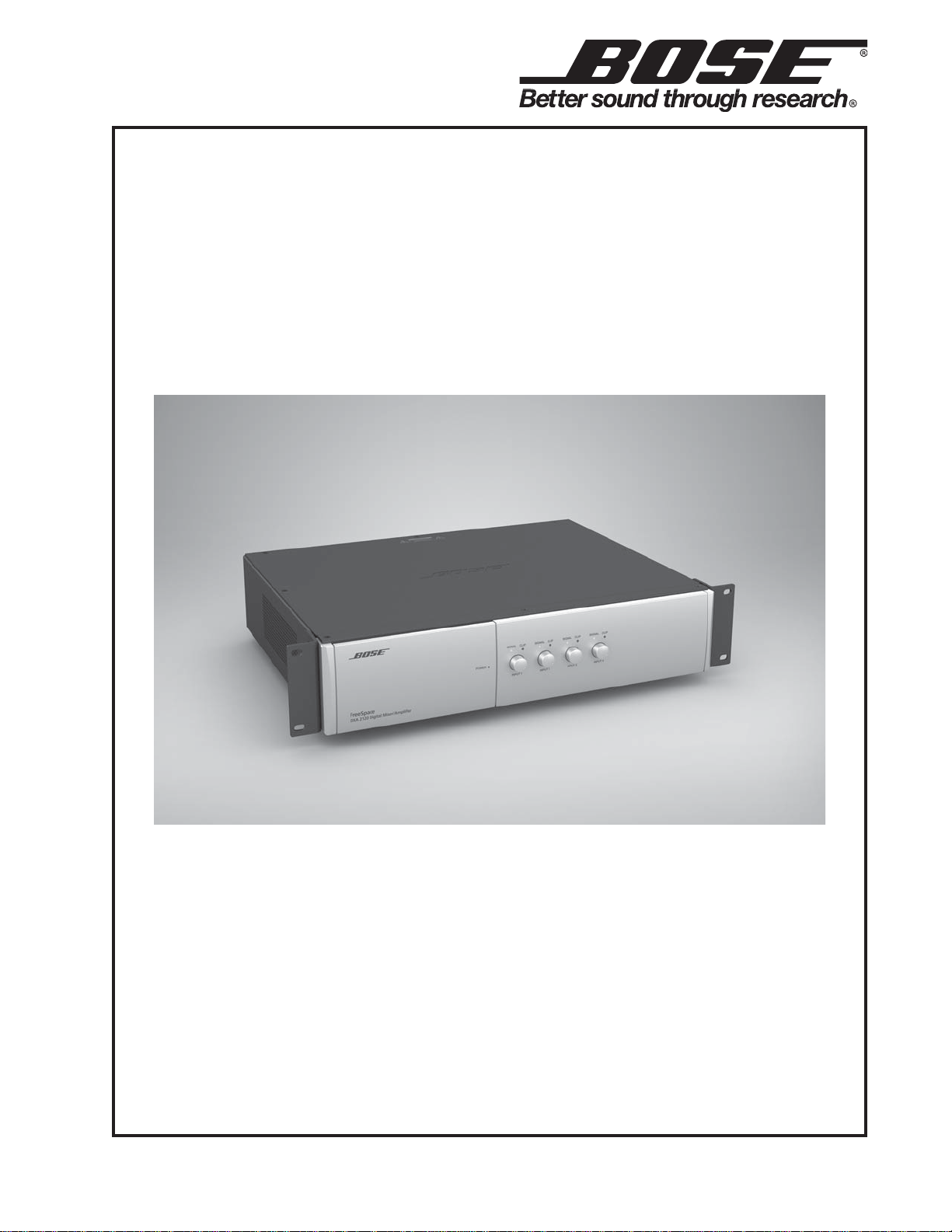
Product Description
The Bose® FreeSpace® DXA 2120 Digital
Mixer/Amplifier integrates digital signal
processing with two 120-watt output
channels. Designed as a mixer/router for
business music applications, it features
an LCD panel and control buttons behind the front cover for ready access and easy configuration.
The mixer/amplifier provides six inputs, including 4 Mic/Line inputs, 1 Page input, and 1 Direct
input. The Direct input can override all sources playing on the output channels. Each Mic/Line
input provides both RCA and Euroblock jacks. The Euroblock connectors will accept either a Mic
or Line level input. The RCA jacks accept Line level inputs only.
Two output channels are wired for 120 watts at 4 ohms each. For 70/100 volt applications, a
jumper is required for proper configuration. In 70/100V applications, the two outputs will operate
at 100 watts per channel. A third output is available for an auxiliary line out.
Additional features include:
• Signal Mixing: In Mixer Mode, simultaneously combines up to four inputs for any of the
three outputs.
• Signal Routing: In Dual Mono Select Mode, one or two inputs go to each of two outputs in
different zones and can be remotely selected. Or in Stereo Select Mode, two stereo sources
go to one output zone and can be remotely selected.
• Opti-voice
®
Paging: Provides a smooth transition between music and page signals.
• Dynamic Equalization: Maintains tonal balance at all listening levels.
• Room Equalization: Allows easy adjustment of tonal balance in each zone.
• Communications Port: Includes an RS-232 serial port in reserve for system updates.
• Back-up Power: Provides an input terminal for a +24V DC back-up power source.
POWER
Supplied with the product
Included Connectors:
• 3-terminal input connectors (4) for wiring source equipment to 1 - 4 Line/Mic input Euroblock
jacks.
• 4-terminal input connectors (2) for wiring to the single Page and single Direct input jacks.
• 6-terminal input connector (1) for wiring to interface wall controls to the wall panel input jack.
• 3-terminal output connector (1) for wiring to the AUX-out jack.
Included placement aids:
• Non-skid rubber feet (4) for stable placement on a solid, level surface.
• Rack ears (2) with mounting hardware for installation in a rack.
Mixer/Amplifier Accessories
• FreeSpace DXA volume control - A wall-mountable plate with volume control knob that fits
into a standard U.S. double-gang junction.box.
• FreeSpace DXA volume control with A/B select - A wall-mountable plate that fits into a
standard U.S. double-gang junction box. It features volume control and A/B select knobs for
remote source selection.
4
Page 5
Hardware Description
Front panel with open compartment
1
5
6
2
7
System Controls
1 - LCD panel - Displays menu selection for
configuring and viewing system settings.
2 - Directional buttons - Navigate system
menus and setting options as shown on the
LCD.
3 - Select button - Confirms selections and
settings in the system menus.
4 - Power LED - Blue light indicates the
system is on. No light when it is off.
5 - Signal and Clip LEDs - Show signal
states for OUPUT 1, OUTPUT 2, PAGE and
DIRECT.
Signal Unlit = No signal
Clip Unlit = No clipping
Signal Green = Signal present
Clip Red = Clipping
6 - Gain knobs - Adjust gain for OUTPUT 1,
OUTPUT 2 and PAGE.
3
4
8
7 - Bass and Treble knobs - Adjust tonal
balance for OUTPUT 1 and OUTPUT 2.
Control Compartment
8 - Enclosure Door - Conceals system
controls.
Input Controls
9 - SIGNAL and CLIP LEDs - Show signal
states for Inputs 1 - 4.
Signal Unlit = No signal
Clip Unlit = No clipping
Signal Green = Signal present
Clip Red = Clipping
10 - Gain knobs - Adjust gain for INPUT 1 INPUT 4.
9
10
Front panel with compartment closed
1
1 Latch location – Provides access to system controls. 2 Power status window – Reveals Power LED.
2
5
Page 6
Hardware Description
Rear Panel
1
2
3
4
Audio source inputs
1 - INPUT 1 of 4 - Unbalanced RCA audio
input jack.
2 - MIC/LINE switch - To adjust for the type
if signal input. (Mic connections require
using Euroblock input jacks.)
3 - INPUT 2 of 4 - Balanced Euroblock audio
input jack.
4 - DIRECT INPUT - Balanced override input
jack.
5 - PAGE INPUT - Balanced audio input
jack.
5
14
6
8
7
9 10
13
Communication
14 - COM - RS-232 serial port for system
updates.
Wall Plates
The FreeSpace
®
DXA 2120 is designed to be
compatible with the following Bose user
interfaces:
• Bose Volume Control User Interface
(PC 041966)
• Bose Volume Control with A/B Select
User Interface (PC 041967)
11
12
Outputs
6 - AUX OUTPUT - Line-level signal output
for other amplified equipment.
7 - OUTPUT 1 of 2 - Speaker connections
for two powered outputs of 70V, 100V or 4
ohms.
Control Input
8 - REMOTE - Input jack for Volume control
and Volume control with A/B select wallplate
user interfaces.
Power
9 - BACKUP POWER - For connection to
backup power source.
10 - POWER ON/OFF - AC power switch
11 - FUSE - 120V T6.3A/250V L or 240V
T3.15A/250 L.
12 - AC mains line cord jack - AC line
voltage input.
13 - 120V/220-240V switch - Switches
between 120V and 220-240V AC input
voltage. This switch is not provided on 100V
AC input voltage models.
6
Page 7
System Setup
This section provides instructions on setting
the system for preferred operation. To make
these settings, the system must be connected to power and the AC POWER switch
set to ON.
Rear connection panel
POWER
switch
Front control compartment
AC power cord
jack
• When the system is unlocked, you can
navigate to system setup options.
• Use the arrow and SELECT buttons to
move through the menus and change
settings for the equipment used and the
type of connections made in your instal lation.
• Notice the type of setting in each field:
- Level changes (designated by Lvl) are
made using the GAIN knobs only. These
levels appear in the menu field, but
cannot be changed in the menu.
- Adjustments (designated by Adj) are
made in the menu. To do so:
1. Activate the field by pressing SELECT.
2. Using the up or down arrow, adjust the
value.
3. Press SELECT to confirm the setting
and move on.
Selecting an operation mode
POWER
LED
Note: When the system is unplugged, or if a
power loss occurs, these system settings
are retained in flash memory. However,
continuous system operation during a power
loss requires the use of an optional backup
power source.
System Setup Procedure
When first turned on, pressing any button
next to the LCD activates the display.
Front control panel
Arrow
buttons
SELECT button
• If the system is locked, simultaneously
press the left and right arrow buttons and
hold for five seconds. Lockout Off appears.
Arrow buttons to
the right of the
LCD move forward,
back, up, and down
through menus.
An asterisk (*) marks
the selection made.
Some of the setting menus available for
selections depend on the mode of operation
you choose.
Pressing the right arrow button brings up the
initial selection menu so you can chose the
mode you need:
• Mixer mode: The system can mix up to
four mic/line inputs to each of the two output
channels for use in one or two zones.
• Stereo Select mode: With up to two
stereo sources connected and using both
output channels, the system provides stereo
sound to a single output zone.
• Dual Mono Select mode: With two input
souces connected to each of the two output
channnels, the system provides audio in two
zones.
• Utility - Includes system lockout and an
option to restore all settings to the factory
defaults.
7
Page 8

Specifications
Audio Inputs
Mic Inputs (4 - Balanced): Connectors: 3-pin Euroblock
Input Range: 20 - 20kHz
Input Impedance: 2k ohms (Mic)
25k ohms (Line)
Equivalent Input Noise: -122dB
Line Inputs (4 - Unbalanced): Connectors: Dual RCA (summed to mono)
Input Range: 20 20kHz
Input Impedance: 10k ohms
Maximum Input Level: +10dBu
Page Input (1 - Balanced): Connector: 4-pin Euroblock
Input Range: 20 - 20kHz
Input Impedance: 400 ohms
Equivalent Noise Input: -122dB
Direct Input (1 - Balanced): Connector: 3-pin Euroblock
Input Range: 20 - 20kHz
Input Impedance: 18k ohms
Maximum Input Level: +8dBu
Audio Outputs
Amplifier Outputs (2): Connectors: 5 Terminal Reverse
Euroblock
Minimum Load: 49 ohms @ 70V
98 ohms @ 100V
Output Impedance: 4 ohms
Aux Output (1): Connector: 3-pin Euroblock
Output Impedance: 400 ohms
Maximum Output Level: 2.2 dBV
Performance
Amplifier Power: 120W @ 4 ohms, 100W @ 70/100V
THD (at full rated power): < 0.5%
Crosstalk (below rated power, 1 kHz): < -60 dBV
Signal-to-Noise ratio: 75dB (below rated power, A-weighted)
Frequency Response: 40Hz - 16kHz (+0/-3dB)
Dynamic Range: 83dB
Sampling Rate: 44.1kHz
8
Page 9

Specifications (continued)
A/D and D/A Converters: 24-bit
Communication Port: RS-232 serial port
LED Status Indicators: Power - blue; Signal present - green; Clip - red
Power
Mains Voltage: 100 to 240VAC; 50 to 60Hz
AC Power Consumption: Idle: 39W
Active: 350W
Fuse Type: 120V T6.3A/250 or 240V T3.15A/250 L
DC Backup Power: +24V (+/- 1%)
Connector: 2-terminal barrier strip
Input Voltage Level: +24V
Minimum Input Power: 50W
Maximum Output Power: 150W
Mechanical
Dimensions: 3.5” H x 16.63” W x 13.5” D (8.9 x 42.2 x 34.3 cm)
Weight: Unpackaged: 31.8 lbs
Shipping weight: 39.9 lbs
Environmental
Operating Temperature: 0 - 40 degrees C
Storage Temperature: -40 - 70 degrees C
Humidity: 40 - 90%
9
Page 10

ELECTROSTATIC DISCHARGE SENSITIVE (ESDS)
DEVICE HANDLING
This unit contains ESDS devices. We recommend the following precautions when repairing,
replacing or transporting ESDS devices:
• Perform work at an electrically grounded work station.
• Wear wrist straps that connect to the station or heel straps that connect to conductive
floor mats.
• Avoid touching the leads or contacts of ESDS devices or PC boards even if properly
grounded. Handle boards by the edges only.
• Transport or store ESDS devices in ESD protective bags, bins, or totes. Do not insert
unprotected devices into materials such as plastic, polystyrene foam, clear plastic bags,
bubble wrap or plastic trays.
PART LIST NOTES
1. This part is not normally available from Customer Service. Approval from the Field Service
Manager is required before ordering.
2. The individual parts located on the PCBs are listed in the Electrical Part List.
3. This part is critical for safety purposes. Failure to use a substitute replacement with the
same safety characteristics as the recommended replacement part might create shock, fire
and/or other hazards.
4. This part is referenced for informational purposes only. It is not stocked as a repair part.
Refer to the next higher assembly for a replacement part.
10
Page 11
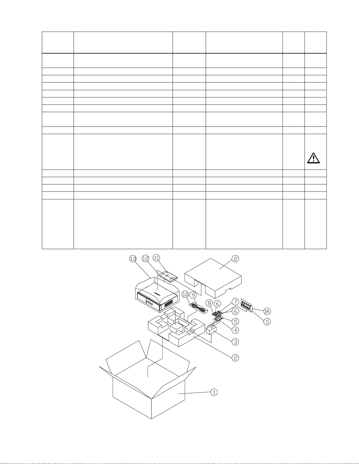
PACKAGING PART LIST
FreeSp ace® DXA 2120 Amplifier/Mixer (see Figure 1)
Item
Number
CARTON KIT, I NCLUDES ITEMS
1, 2 AND 13
1 CARTON 298708 1437-8501+0-3 1
2 PE FOAM - 1493-1761+0 2
3 WHITE BOX - 1480-9401+0 1 4
4 RACK EAR 298706 4135-6291+0 2
5 POLYBAG, .04x5x9 - 1497-1932-0 2 4
6 POLYBAG, .04x5x6 - 1497-2042-0 2 4
7 SCREW, MACHINE, FLAT-CS
(USED WITH RACK EARS)
8 RUBBER FOOT 298707 4157-1121+0 4
9 AC POWER CORD, US/C AN 298165 7012-7340+0 1 3
AC POWER CORD, EURO 298166 7012-6601+0
AC POWER CORD, JAPAN 298167 7012- 553 0+0
AC POWER CORD, UK 298168 7012-660 3+0
AC POWER CORD, AUS 298169 7012- 543 0+0
10 POLYBAG, 10’x14’ - 1497-4122-0 1 4
11 OWNERS MANUAL 298710 4301-7240+0 1
12 PO LY BAG FOR MANUAL - 1497-1062+0 1 4
13 PO LYBAG FOR UNIT - 1497-8012+0 1 4
14 MATING CONN KIT, REAR I/O;
INCLUDES:
– MIC/LINE CONN, 3 POS
– DIRECT/PAG E CONN, 4 POS
– RMT INPUT CON N, 6 POS
– AUX OUTPUT CONN, 3 POS
– SPKR OUTPUT CONN, 5 POS
Description Bose®
Part
Number
298709 SVC-MIXER14+PKG 1
- 2901-4012+3000 6 4
298704
-
-
-
-
-
Vendor Part Number Qty. Note
-
2113-3143+0
2113-3147+0
2113-3149+0
2113-3143+0
2113-3272+0
1
4
2
1
1
2
Figure 1. FreeSpace DXA 2120 Packaging View
11
Page 12
MAIN PART LIST
V
C
FreeSp ace® DXA 2120 Amplifier/Mixer (see Figure 2)
Item
Number
1 TOP COVER, CHA S SIS 1405-8601+0 298 705 1
2 DSP/MCU PCB ASSEMBLY SVC-MIXER14+DSP 298689 1 2
3 BRACKET FOR DSP PCB 4135-6371+0 - 1 4
4 POWER SUPPLY PCB ASSY SVC-MIXER14+PSU 298690 1 2
5 FUSE HOLDER 4153-1100+0 - 1 3,4
6 AC JACK, I EC POWER 2113-3050+0 - 1 3 ,4
7 SHIELD P LA TE, RCA JACK 1454-2 530+ 0 - 1 4
8 I/O PCB ASS EMBLY SVC-M IXE R14+ I/O 298701 1 2
9 RCA IN/A-D BUFF PCB ASSY
( PAR T OF ITEM 8 ABOVE)
10 CHASSIS 1405-8704+0 - 1 4
11 RS-232 PC B ASSEMB LY SV C- M IXE R14+ 232 298702 1 2
12 RACK EAR 4135-6291+0 298706 2
13 SPEAKER PCB ASSEMBLY SVC-MIXER14+SPK 298700 1 2
14 AC VOL T SELECT PCB ASS Y SVC-MIXE R14+ V OLT 298699 1 2
15 FRONT PANEL CONTROL
AND DISPLAY PCB ASSY
16 FRONT PANEL, CHASSIS 1405-9502+0 - 1
17 LIGHT PIPE 4155-1861+0 298517 9
18 FRONT PANEL, FIXED SIDE
WITH END CA P
19 FRONT PANEL, ALUM, RT 1405-8901+0 - 1
20 KNOB, INPUT VOLUME
(INCLUDES ALL 4 KNOBS)
21 DOOR ASSEMBLY SVC-MIXER14+DOOR 298682 1
22 M AGNET , DOOR ASSY 4110-0001+0 2 4
23 END CAP, F RON T PANEL,
LE FT SIDE
24 FRONT PANEL, LEFT 1467-6301+0 - 1
25 SPRING PLATE 4135-6381+0 - 2
26 COVER FOR SPRING 4155-1911+0 - 2
27 KNOB, PUSH 2447-3201+0 - 1
28 AC INP UT XFMR (120/240V) 1806-3927+0 298 698 1 3
28 AC INP UT XFMR (100V ) 1806- 3928+0 301 561 1 3
29 24V BACKUP P/S PCB ASSY SVC-MIXE R14+DC24 298693 1 2
30 HEAT S INK FO R DC- DC P CB 5400- 9761+0 - 1 4
31 BRACKET, FAN GUIDE 4135- 6281+0 - 1 4
32 OUTPUT XFMR, CV, 70/100V 1806-3943+0 298697 2 3
Description
endo r Part Number Bose®
Part
Number
SVC-MIXER14+RCA - 1 2
SVC-MIXER14+CTRL 298685 1 2
SVC-MIXER14+CAP 298683 1
SV
-MIXER14+KNOB 328113001S
1467-6401+0 298681 1
Qty. Note
4
12
Page 13
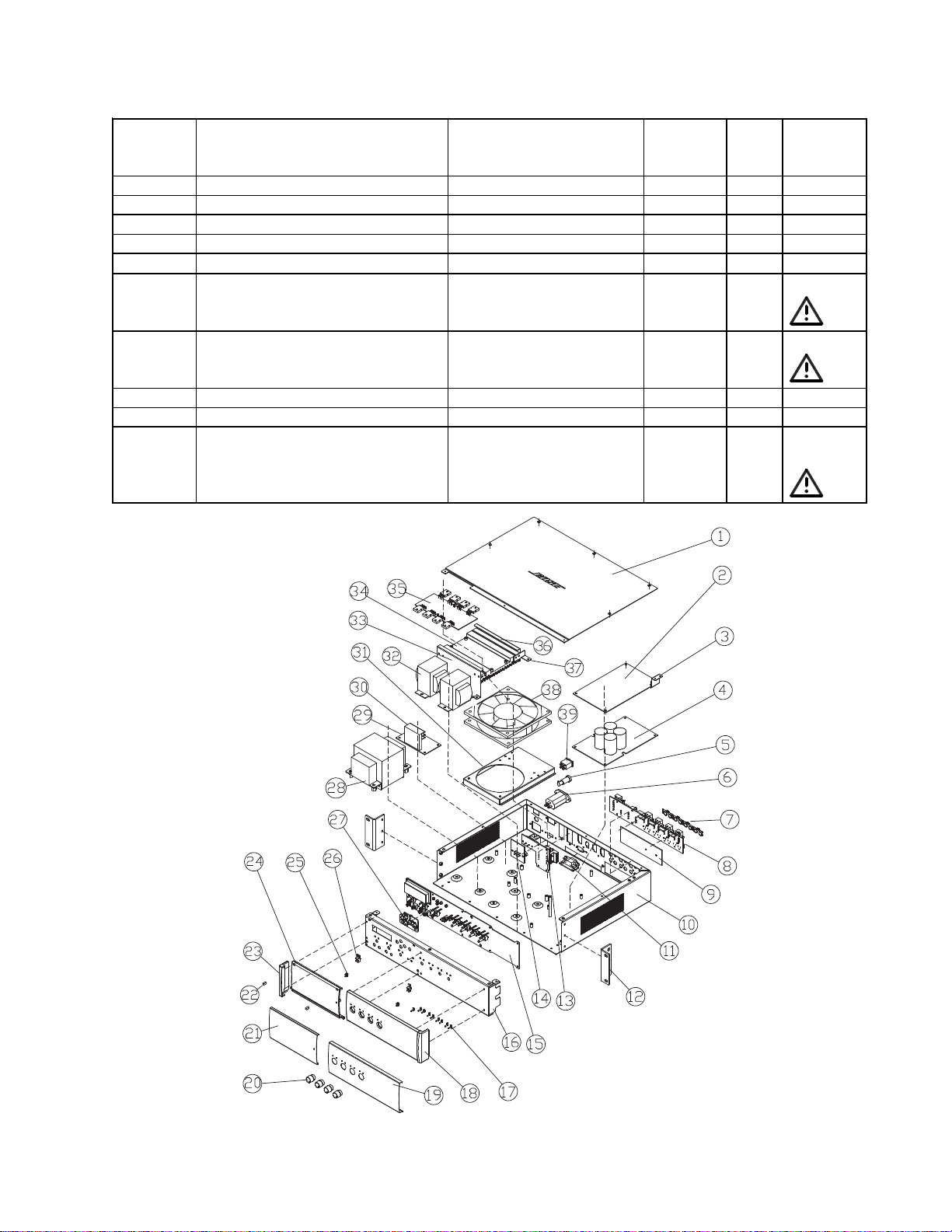
MAIN PART LIST
V
FreeSp ace® DXA 2120 Amplifier/Mixer (see Figure 2)
Item
Number
33 BRACKET C FO R HE A T SINK 4135-6361+0 - 1 4
34 HEATSINK 5400-9721+0 - 1 4
35 AMPLIFIER PCB ASSEMBLY SVC-MIXER14+AMP 298695 1 2
36 BR ACKET B FOR HEAT SINK 4135-6261+0 - 1 4
37 BR ACKET A FOR HEAT SINK 4135-6251+0 - 1 4
38 FAN, DC, 24V, 2400 RP M 8913-0005+0 298703 1 3
39 AC POWER SWITCH 5200-4942+0 - 1 3,4
- RIBBON CABLE 7012-7870+0 298688 3
- LCD DISPLAY 8902-0005+0 298686 1
- F USE T6.3A 250V 5X20 UL
(120V UNITS)
FUSE T3.15A 250V 5X20MM
UR & SE MKO (220-240V)
Description
endo r Part Number Bose®
Part
Number
5120-0040+0
5120-0079+0
177311-
06300
177311-
03150
Qty. Note
1 3,4
Figure 2. FreeSpace DXA 2120 Amplifier/Mixer Exploded View
13
Page 14
ELECTRICAL PART LIST
Control PCB Assembly
Resistors
Reference
Designator
R401 100 OHM, RCF, 1/4W, 5%, ATS 4705-101J+C 4
R402 100 OHM, RCF, 1/4W, 5%, ATS 4705-101J+C 4
R403 100 OHM, RCF, 1/4W, 5%, ATS 4705-101J+C 4
R404 100 OHM, RCF, 1/4W, 5%, ATS 4705-101J+C 4
R405 100 OHM, RCF, 1/4W, 5%, ATS 4705-101J+C 4
R406 100 OHM, RCF, 1/4W, 5%, ATS 4705-101J+C 4
R407 100 OHM, RCF, 1/4W, 5%, ATS 4705-101J+C 4
R408 100 OHM, RCF, 1/4W, 5%, ATS 4705-101J+C 4
R409 300 OHM, RCF, 1/4W, 5%, ATS 4705-301J+C 4
R410 300 OHM, RCF, 1/4W, 5%, ATS 4705-301J+C 4
R411 300 OHM, RCF, 1/4W, 5%, ATS 4705-301J+C 4
R412 300 OHM, RCF, 1/4W, 5%, ATS 4705-301J+C 4
R413 300 OHM, RCF, 1/4W, 5%, ATS 4705-301J+C 4
R414 300 OHM, RCF, 1/4W, 5%, ATS 4705-301J+C 4
R415 300 OHM, RCF, 1/4W, 5%, ATS 4705-301J+C 4
R416 300 OHM, RCF, 1/4W, 5%, ATS 4705-301J+C 4
R421 10K, RCF, 1/4W, 5%, ATS 4705-103J+C 4
R422 10K, RCF, 1/4W, 5%, ATS 4705-103J+C 4
R423 10K, RCF, 1/4W, 5%, ATS 4705-103J+C 4
R424 10K, RCF, 1/4W, 5%, ATS 4705-103J+C 4
R425 10K, RCF, 1/4W, 5%, ATS 4705-103J+C 4
R430 300 OHM, RCF, 1/4W, 5%, ATS 4705-301J+C 4
Description Vendor Part
Number
Capacitors
Note
Reference
Designator
C401 0.1uF, CC, 50V, 10%, RLT, 5x5 150F-104K+K-II 4
C402 0.1uF, CC, 50V, 10%, RLT, 5x5 150F-104K+K-II 4
C403 0.1uF, CC, 50V, 10%, RLT, 5x5 150F-104K+K-II 4
C404 0.1uF, CC, 50V, 10%, RLT, 5x5 150F-104K+K-II 4
C405 0.1uF, CC, 50V, 10%, RLT, 5x5 150F-104K+K-II 4
C406 0.1uF, CC, 50V, 10%, RLT, 5x5 150F-104K+K-II 4
C407 0.1uF, CC, 50V, 10%, RLT, 5x5 150F-104K+K-II 4
C408 0.1uF, CC, 50V, 10%, RLT, 5x5 150F-104K+K-II 4
C409 0.1uF, CC, 50V, 10%, RLT, 5x5 150F-104K+K-II 4
C410 0.1uF, CC, 50V, 10%, RLT, 5x5 150F-104K+K-II 4
C411 0.1uF, CC, 50V, 10%, RLT, 5x5 150F-104K+K-II 4
C421 0.1uF, CC, 50V, 10%, RLT, 5x5 150F-104K+K-II 4
C422 0.1uF, CC, 50V, 10%, RLT, 5x5 150F-104K+K-II 4
C423 0.1uF, CC, 50V, 10%, RLT, 5x5 150F-104K+K-II 4
C424 0.1uF, CC, 50V, 10%, RLT, 5x5 150F-104K+K-II 4
C425 0.1uF, CC, 50V, 10%, RLT, 5x5 150F-104K+K-II 4
C431 0.1uF, CC, 50V, 10%, RLT, 5x5 150F-104K+K-II 4
C432 0.1uF, CC, 50V, 10%, RLT, 5x5 150F-104K+K-II 4
C433 10uF, CE, 16V, 20%, RLT, 4X5, SSK, SHOEI 157D-106M+K-GII 4
C434 10uF, CE, 16V, 20%, RLT, 4X5, SSK, SHOEI 157D-106M+K-GII 4
Description Vendor Part
Number
Note
14
Page 15
ELECTRICAL PART LIST
Control PCB Assembly
LEDs
Reference
Designator
LED401 LED, SLR342-MG3F, GN (ROHM) 3700-2570+G 4
LED402 LED, SLR342-MG3F, GN (ROHM) 3700-2570+G 4
LED403 LED, SLR342-MG3F, GN (ROHM) 3700-2570+G 4
LED404 LED, SLR342-MG3F, GN (ROHM) 3700-2570+G 4
LED405 LED, CY, D3X8, GN 3700-3616+G 4
LED406 LED, CY, D3X8, GN 3700-3616+G 4
LED407 LED, CY, D3X8, GN 3700-3616+G 4
LED408 LED, CY, D3X8, GN 3700-3616+G 4
LED409 LED, SC, 3.1X3.8, L0.4, RD 3700-1530+R 4
LED410 LED, SC, 3.1X3.8, L0.4, RD 3700-1530+R 4
LED411 LED, SC, 3.1X3.8, L0.4, RD 3700-1530+R 4
LED412 LED, SC, 3.1X3.8, L0.4, RD 3700-1530+R 4
LED413 LED, CY, D3X8, RD 3700-3617+R 4
LED414 LED, CY, D3X8, RD 3700-3617+R 4
LED415 LED, CY, D3X8, RD 3700-3617+R 4
LED416 LED, CY, D3X8, RD 3700-3617+R 4
LED421 LED, CY, D3X8, BL 3700-3615+B 4
Reference
Designator
VR408 VR, 20KBX2, RV09ACF-40-15B, SCREW ADJ 4751-1250+0 4
VR409 VR, 20KBX2, RV09ACF-40-15B, SCREW ADJ 4751-1250+0 4
VR410 VR, 20KBX2, RV09ACF-40-15B, SCREW ADJ 4751-1250+0 4
VR411 VR, 20KBX2, RV09ACF-40-15B, SCREW ADJ 4751-1250+0 4
VR405 VR, ROTARY, 20KB, L20 SHAFT, 40 TEETH,
RV09ACF-40-20K
VR406 VR, ROTARY, 20KB, L20 SHAFT, 40 TEETH,
RV09ACF-40-20K
VR407 VR, ROTARY, 20KB, L20 SHAFT, 40 TEETH,
RV09ACF-40-20K
VR401 VR, ROTARY, 20KB, L25, SHAFT, FLAT,
RV09ACF-40-25F
VR402 VR, ROTARY, 20KB, L25, SHAFT, FLAT,
RV09ACF-40-25F
VR403 VR, ROTARY, 20KB, L25, SHAFT, FLAT,
RV09ACF-40-25F
VR404 VR, ROTARY, 20KB, L25, SHAFT, FLAT,
RV09ACF-40-25F
K401 SW, TACT, SPST, SKQNAED010, H=5, ALPS 5200-4847+0-01 4
K402 SW, TACT, SPST, SKQNAED010, H=5, ALPS 5200-4847+0-01 4
K403 SW, TACT, SPST, SKQNAED010, H=5, ALPS 5200-4847+0-01 4
K404 SW, TACT, SPST, SKQNAED010, H=5, ALPS 5200-4847+0-01 4
K405 SW, TACT, SPST, SKQNAED010, H=5, ALPS 5200-4847+0-01 4
CN07A CONN, FFC, 20 PIN, P=1.0MM (HORIZONTAL) 2101- 3051+0 4
CN08A CONN, FFC, 20 PIN, P=1.0MM (HORIZONTAL) 2101- 3051+0 4
CN09A CONN, FFC, 20 PIN, P=1.0MM (HORIZONTAL) 2101- 3051+0 4
Description Vendor Part
Number
Miscellaneous
Description Vendor Part
Number
4751-1260+0 4
4751-1260+0 4
4751-1260+0 4
4751-1270+0 4
4751-1270+0 4
4751-1270+0 4
4751-1270+0 4
Note
Note
15
Page 16
ELECTRICAL PART LIST
Control PCB Assembly
Miscellaneous (continued)
Reference
Designator
LCD401 HEADER, 16P, P2. 54, ST, MALE 2101-3141+0 4
\LED401 LED SPACER, H=12.0MM 4171-0081+0 4
\LED402 LED SPACER, H=12.0MM 4171-0081+0 4
\LED403 LED SPACER, H=12.0MM 4171-0081+0 4
\LED404 LED SPACER, H=12.0MM 4171-0081+0 4
\LED405 LED SPACER, H=8.5MM 4157-0331+0 4
\LED406 LED SPACER, H=8.5MM 4157-0331+0 4
\LED407 LED SPACER, H=8.5MM 4157-0331+0 4
\LED408 LED SPACER, H=8.5MM 4157-0331+0 4
\LED409 LED SPACER, H=12.0MM 4171-0081+0 4
\LED410 LED SPACER, H=12.0MM 4171-0081+0 4
\LED411 LED SPACER, H=12.0MM 4171-0081+0 4
\LED412 LED SPACER, H=12.0MM 4171-0081+0 4
\LED413 LED SPACER, H=8.5MM 4157-0331+0 4
\LED414 LED SPACER, H=8.5MM 4157-0331+0 4
\LED415 LED SPACER, H=8.5MM 4157-0331+0 4
\LED416 LED SPACER, H=8.5MM 4157-0331+0 4
\LED421 LED SPACER, H=8.5MM 4157-0331+0 4
Description Vendor Part
Number
Note
16
Page 17
ELECTRICAL PART LIST
DC24 PCB Assembly
Resistors
Reference
Designator
R701 100 OHM, RCF, 1/4W, 5%, ATS 4705-101J+C 1 4
R702 10K, RCF, 1/4W, 5%, ATS 4705-103J+C 1 4
R703 15K, RCF, 1/4W, 5%, ATS 4705-153J+C 1 4
R704 4.7K, RCF, 1/4W, 5%, ATS 4705-472J+C 1 4
R705 4.7K, RCF, 1/4W, 5%, ATS 4705-472J+C 1 4
R706 4.7K, RCF, 1/4W, 5%, ATS 4705-472J+C 1 4
R708 15K, RCF, 1/4W, 5%, ATS 4705-153J+C 1 4
R710 150K, RCF, 1/4W, 5%, ATS 4705-154J+C 1 4
R711 24K, RCF, 1/4W, 5%, ATS 4705-243J+C 1 4
R712 3.3K, RCF, 1/4W, 5%, ATS 4705-332J+C 1 4
R713 3.3K, RCF, 1/4W, 5%, ATS 4705-332J+C 1 4
R714 4.7K, RCF, 1/4W, 5%, ATS 4705-472J+C 1 4
R715 4.7K, RCF, 1/4W, 5%, ATS 4705-472J+C 1 4
R716 47 OHM, RCF, 1/4W, 5%, ATS 4705-470J+C 1 4
R717 47 OHM, RCF, 1/4W, 5%, ATS 4705-470J+C 1 4
R718 22 OHM, RCF, 1/2W, 5%, ATS 4707-220J+C 1 4
R719 22 OHM, RCF, 1/2W, 5%, ATS 4707-220J+C 1 4
R720 22 OHM, RCF, 1/2W, 5%, ATS 4707-220J+C 1 4
Reference
Designator
C701 220uF, CE, 6.3V, 20%, RLT, 5X11,
SHOEI
C702 1000pF, CC, 50V, T-10%, 5X5, RLT,
335321025T
C703 47uF, CE, 35V, 20%, RLT, P5.0, 5X11,
YK, RUBYCON
C704 0.1uF, CC, 50V, 10%, RLT, 5x5 150F-104K+K-II 1 4
C705 0.0047uF, CC, 50V, 10%, AT, 3.8x2.5,
MONO
C706 0.0047uF, CC, 50V, 10%, AT, 3.8x2.5,
MONO
C707 0.1uF, CC, 50V, 10%, RLT, 5x5 150F-104K+K-II 1 4
C708 2200uF, CE, 35V, 20%, RL, 16x31.5 157Q-228M+5-5$ 1 4
C709 0.1uF, CC, 50V, 10%, RLT, 5x5 150F-104K+K-II 1 4
C710 1000pF, CC, 50V, T-10%, 5X5, RLT,
335321025T
C711 100uF, CE, 50V, 20%, RLT, 8X12 157F-107M+K-OW 1 4
C712 100uF, CE, 50V, 20%, RLT, 8X12 157F-107M+K-OW 1 4
C713 0.1uF, CC, 50V, 10%, RLT, 5x5 150F-104K+K-II 1 4
C714 0.1uF, CC, 50V, 10%, RLT, 5x5 150F-104K+K-II 1 4
C715 100uF, CE, 50V, 20%, RLT, 8X12 157F-107M+K-OW 1 4
C716 100uF, CE, 50V, 20%, RLT, 8X12 157F-107M+K-OW 1 4
C717 0.1uF, CC, 50V, 10%, RLT, 5x5 150F-104K+K-II 1 4
C718 0.1uF, CC, 50V, 10%, RLT, 5x5 150F-104K+K-II 1 4
Description Vendor Part
Number
Capacitors
Description Vendor Part
Number
157B-227M+K-IUI 1 4
150F-102K+K-II 1 4
157Q-476M+K-IUY 1 4
150F-472K+2-GD 1 4
150F-472K+2-GD 1 4
150F-102K+K-II 1 4
Qty. Note
Qty. Note
17
Page 18
ELECTRICAL PART LIST
V
DC24 PCB Assembly
Diodes
Reference
Designator
D702 SB580, DO-201AD, RL 480B-5800+5 1 4
D703 SB580, DO-201AD, RL 480B-5800+5 1 4
D704 SB580, DO-201AD, RL 480B-5800+5 1 4
D705 SB580, DO-201AD, RL 480B-5800+5 1 4
D706 SB540-F54, PANJIT 4840-8560+5 1 4
D707 SB540-F54, PANJIT 4840-8560+5 1 4
D708 SB540-F54, PANJIT 4840-8560+5 1 4
D709 SB540-F54, PANJIT 4840-8560+5 1 4
Reference
Designator
Q701 2SC1845, FE, RLT 4860-0190+K 1 4
Q702 2SA992, HFE, 300-600, RLT 4850-992F+K 1 4
Q703 2SA992, HFE, 300-600, RLT 4850-992F+K 1 4
Q704 2SC1845, FE, RLT 4860-0190+K 1 4
Q705 FET , IRFZ44NPBF, TO-220, 60V, 50A 490F-Z440+5 1 4
Q706 FET , IRFZ44NPBF, TO-220, 60V, 50A 490F-Z440+5 1 4
Q707 2SA992, HFE, 300-600, RLT 4850-992F+K 1 4
Description Vendor Part
Number
Transistors
Description Vendor Part
Number
Integrated Circuits
Qty. Note
Qty. Note
Reference
Designator
U701 PWM CONTROLLER, TL494CN 3131-6180+0 1 4
Reference
Designator
T701 TRANSFORMER, DC-DC, 24V, 150W,
Description Vendor Part
Number
Miscellaneous
Description
endor Part
Qty. Note
Qty. Note
Number
1806-3933+0 1 4
24VX2, 15VX2
F701
FUSE, T10A H, 250V
(BOSE
®
PART NUMB E R 325634-0010)
5120-0110+0
1 3
F701A FUSE HOLDER 4132-1011+0 1 4
F701B FUSE HOLDER 4132-1011+0 1 4
B- WIRE-CONN, 1P, #18, UL1015, L=300,
7012-7832+0 1 4
BLK , 250-TERMIN AL
B+ WIRE-CONN, 1P, #18, UL1015, L=250,
7012-7831+0 1 4
R ED, 250-TERMINAL
F ET SCREW, B-TI TE, BIND HEAD, M3X 8 ,
2954-3008+3000 2 4
CR O SS- RECE SS, BZ
FET MICA, T0-220 3100-8000+0 2 4
FET INSULATION BUSHING, 115DEG.C 4154-0841+0 2 4
FET H EAT SI NK , DC, 56X46 5400-9761+0 1 4
18
Page 19

ELECTRICAL PART LIST
Digital Signal Processor (DSP) PCB Assembly
Resistors
Reference
Designator
R201 1K, RMG, 1/16W, 5%, 0603/1608 4723-102J+P 4
R202 1K, RMG, 1/16W, 5%, 0603/1608 4723-102J+P 4
R203 10K, RMG, 1/16W, 5%, 0603/1608 4723-103J+P 4
R204 10K, RMG, 1/16W, 5%, 0603/1608 4723-103J+P 4
R205 1K, RMG, 1/16W, 5%, 0603/1608 4723-102J+P 4
R206 1K, RMG, 1/16W, 5%, 0603/1608 4723-102J+P 4
R207 10K, RMG, 1/16W, 5%, 0603/1608 4723-103J+P 4
R208 1K, RMG, 1/16W, 5%, 0603/1608 4723-102J+P 4
R209 1K, RMG, 1/16W, 5%, 0603/1608 4723-102J+P 4
R210 10K, RMG, 1/16W, 5%, 0603/1608 4723-103J+P 4
R211 10K, RMG, 1/16W, 5%, 0603/1608 4723-103J+P 4
R229 10K, RMG, 1/16W, 5%, 0603/1608 4723-103J+P 4
R230 10K, RMG, 1/16W, 5%, 0603/1608 4723-103J+P 4
R231 12.1K, RMG, 1/10W, 1%, 0805 4720-1212+J 4
R232 12.1K, RMG, 1/10W, 1%, 0805 4720-1212+J 4
R233 1.58K, RMG, 1/16W, 1%, 0603 4723-1581+P 4
R234 1.58K, RMG, 1/16W, 1%, 0603 4723-1581+P 4
R235 12.1K, RMG, 1/10W, 1%, 0805 4720-1212+J 4
R236 12.1K, RMG, 1/10W, 1%, 0805 4720-1212+J 4
R237 560 OHM, RMG, 1/16W, 5%, 0603/1608 4723-561J+P 4
R238 47K, RMG, 1/16W, 5%, 0603/1608 4723-473J+P 4
R239 12.1K, RMG, 1/10W, 1%, 0805 4720-1212+J 4
R240 12.1K, RMG, 1/10W, 1%, 0805 4720-1212+J 4
R241 1.58K, RMG, 1/16W, 1%, 0603 4723-1581+P 4
R242 1.58K, RMG, 1/16W, 1%, 0603 4723-1581+P 4
R243 12.1K, RMG, 1/10W, 1%, 0805 4720-1212+J 4
R244 12.1K, RMG, 1/10W, 1%, 0805 4720-1212+J 4
R245 560 OHM, RMG, 1/16W, 5%, 0603/1608 4723-561J+P 4
R246 47K, RMG, 1/16W, 5%, 0603/1608 4723-473J+P 4
R247 12.1K, RMG, 1/10W, 1%, 0805 4720-1212+J 4
R248 1.58K, RMG, 1/16W, 1%, 0603 4723-1581+P 4
R249 12.1K, RMG, 1/10W, 1%, 0805 4720-1212+J 4
R250 100K, RMG, 1/16W, 5%, 0603/1608 4723-104J+P 4
R251 560 OHM, RMG, 1/16W, 5%, 0603/1608 4723-561J+P 4
R252 47K, RMG, 1/16W, 5%, 0603/1608 4723-473J+P 4
R253 12.1K, RMG, 1/10W, 1%, 0805 4720-1212+J 4
R254 1.58K, RMG, 1/16W, 1%, 0603 4723-1581+P 4
R255 12.1K, RMG, 1/10W, 1%, 0805 4720-1212+J 4
R256 560 OHM, RMG, 1/16W, 5%, 0603/1608 4723-561J+P 4
R257 47K, RMG, 1/16W, 5%, 0603/1608 4723-473J+P 4
R258 10K, RMG, 1/16W, 5%, 0603/1608 4723-103J+P 4
R260 10K, RMG, 1/16W, 5%, 0603/1608 4723-103J+P 4
R261 10K, RMG, 1/16W, 5%, 0603/1608 4723-103J+P 4
R262 10K, RMG, 1/16W, 5%, 0603/1608 4723-103J+P 4
R263 10K, RMG, 1/16W, 5%, 0603/1608 4723-103J+P 4
R264 10K, RMG, 1/16W, 5%, 0603/1608 4723-103J+P 4
Description Vendor Part Number Note
19
Page 20

ELECTRICAL PART LIST
Digital Signal Processor (DSP) PCB Assembly
Resistors (continued)
Reference
Designator
R265 1K, RMG, 1/16W, 5%, 0603/1608 4723-102J+P 4
R266 1K, RMG, 1/16W, 5%, 0603/1608 4723-102J+P 4
R267 10K, RMG, 1/16W, 5%, 0603/1608 4723-103J+P 4
R268 10K, RMG, 1/16W, 5%, 0603/1608 4723-103J+P 4
R269 10K, RMG, 1/16W, 5%, 0603/1608 4723-103J+P 4
R270 10K, RMG, 1/16W, 5%, 0603/1608 4723-103J+P 4
R271 1K, RMG, 1/16W, 5%, 0603/1608 4723-102J+P 4
R272 1K, RMG, 1/16W, 5%, 0603/1608 4723-102J+P 4
R273 1K, RMG, 1/16W, 5%, 0603/1608 4723-102J+P 4
R274 1K, RMG, 1/16W, 5%, 0603/1608 4723-102J+P 4
R275 1K, RMG, 1/16W, 5%, 0603/1608 4723-102J+P 4
R276 10K, RMG, 1/16W, 5%, 0603/1608 4723-103J+P 4
R277 10K, RMG, 1/16W, 5%, 0603/1608 4723-103J+P 4
R278 10K, RMG, 1/16W, 5%, 0603/1608 4723-103J+P 4
R279 10K, RMG, 1/16W, 5%, 0603/1608 4723-103J+P 4
R280 10K, RMG, 1/16W, 5%, 0603/1608 4723-103J+P 4
R281 10K, RMG, 1/16W, 5%, 0603/1608 4723-103J+P 4
R282 10K, RMG, 1/16W, 5%, 0603/1608 4723-103J+P 4
R283 10K, RMG, 1/16W, 5%, 0603/1608 4723-103J+P 4
R284 10K, RMG, 1/16W, 5%, 0603/1608 4723-103J+P 4
R287 1K, RMG, 1/16W, 5%, 0603/1608 4723-102J+P 4
R289 100K, RMG, 1/16W, 5%, 0603/1608 4723-104J+P 4
R290 100K, RMG, 1/16W, 5%, 0603/1608 4723-104J+P 4
R291 330 OHM, RMG, 1/16W, 5%, 0603/1608 4723-331J+P 4
R292 330 OHM, RMG, 1/16W, 5%, 0603/1608 4723-331J+P 4
R293 330 OHM, RMG, 1/16W, 5%, 0603/1608 4723-331J+P 4
R296 0 OHM, RMG, 1/16W, 5%, 0603 4723-000J+P 4
R297 100K, RMG, 1/16W, 5%, 0603/1608 4723-104J+P 4
R298 33RX4, RCFA, 1/16W, 5%, 0603 4703-330J+P-04 4
R299 33RX4, RCFA, 1/16W, 5%, 0603 4703-330J+P-04 4
R300 33RX4, RCFA, 1/16W, 5%, 0603 4703-330J+P-04 4
R301 33RX4, RCFA, 1/16W, 5%, 0603 4703-330J+P-04 4
R302 33RX4, RCFA, 1/16W, 5%, 0603 4703-330J+P-04 4
R303 33RX4, RCFA, 1/16W, 5%, 0603 4703-330J+P-04 4
R304 33RX4, RCFA, 1/16W, 5%, 0603 4703-330J+P-04 4
R305 33RX4, RCFA, 1/16W, 5%, 0603 4703-330J+P-04 4
R306 33RX4, RCFA, 1/16W, 5%, 0603 4703-330J+P-04 4
R307 33RX4, RCFA, 1/16W, 5%, 0603 4703-330J+P-04 4
R308 33RX4, RCFA, 1/16W, 5%, 0603 4703-330J+P-04 4
R310 33RX4, RCFA, 1/16W, 5%, 0603 4703-330J+P-04 4
R311 33RX4, RCFA, 1/16W, 5%, 0603 4703-330J+P-04 4
R312 33RX4, RCFA, 1/16W, 5%, 0603 4703-330J+P-04 4
R313 33RX4, RCFA, 1/16W, 5%, 0603 4703-330J+P-04 4
R314 33 OHM, RMG, 1/16W, 5%, 0603/1608 4723-330J+P 4
R316 0 OHM, RMG, 1/16W, 5%, 0603 4723-000J+P 4
R317 0 OHM, RMG, 1/16W, 5%, 0603 4723-000J+P 4
Description Vendor Part Number Note
20
Page 21
ELECTRICAL PART LIST
Digital Signal Processor (DSP) PCB Assembly
Resistors (continued)
Reference
Designator
R318 10 OHM, RMG, 1/16W, 5%, 0603/1608 4723-100J+P 4
R320 10K, RMG, 1/16W, 5%, 0603/1608 4723-103J+P 4
R321 10K, RMG, 1/16W, 5%, 0603/1608 4723-103J+P 4
R322 10K, RMG, 1/16W, 5%, 0603/1608 4723-103J+P 4
R323 330 OHM, RMG, 1/16W, 5%, 0603/1608 4723-331J+P 4
R324 330 OHM, RMG, 1/16W, 5%, 0603/1608 4723-331J+P 4
R325 330 OHM, RMG, 1/16W, 5%, 0603/1608 4723-331J+P 4
R326 330 OHM, RMG, 1/16W, 5%, 0603/1608 4723-331J+P 4
R327 330 OHM, RMG, 1/16W, 5%, 0603/1608 4723-331J+P 4
R328 330 OHM, RMG, 1/16W, 5%, 0603/1608 4723-331J+P 4
R336 0 OHM, RMG, 1/16W, 5%, 0603 4723-000J+P 4
R337 0 OHM, RMG, 1/16W, 5%, 0603 4723-000J+P 4
R338 0 OHM, RMG, 1/16W, 5%, 0603 4723-000J+P 4
R339 0 OHM, RMG, 1/16W, 5%, 0603 4723-000J+P 4
R340 0 OHM, RMG, 1/16W, 5%, 0603 4723-000J+P 4
R341 0 OHM, RMG, 1/16W, 5%, 0603 4723-000J+P 4
R342 0 OHM, RMG, 1/16W, 5%, 0603 4723-000J+P 4
R343 330 OHM, RMG, 1/16W, 5%, 0603/1608 4723-331J+P 4
R344 330 OHM, RMG, 1/16W, 5%, 0603/1608 4723-331J+P 4
R345 330 OHM, RMG, 1/16W, 5%, 0603/1608 4723-331J+P 4
R346 330 OHM, RMG, 1/16W, 5%, 0603/1608 4723-331J+P 4
R347 330 OHM, RMG, 1/16W, 5%, 0603/1608 4723-331J+P 4
R348 330 OHM, RMG, 1/16W, 5%, 0603/1608 4723-331J+P 4
R367 560 OHM, RMG, 1/16W, 5%, 0603/1608 4723-561J+P 4
R369 10K, RMG, 1/16W, 5%, 0603/1608 4723-103J+P 4
R370 2.2K, RMG, 1/16W, 5%, 0603/1608 4723-222J+P 4
R371 1M, RMG, 1/16W, 5%, 0603/1608 4723-105J+P 4
R372 10K, RMG, 1/16W, 5%, 0603/1608 4723-103J+P 4
R373 10K, RMG, 1/16W, 5%, 0603/1608 4723-103J+P 4
R374 10K, RMG, 1/16W, 5%, 0603/1608 4723-103J+P 4
R377 330 OHM, RMG, 1/16W, 5%, 0603/1608 4723-331J+P 4
R378 330 OHM, RMG, 1/16W, 5%, 0603/1608 4723-331J+P 4
R379 10K, RMG, 1/16W, 5%, 0603/1608 4723-103J+P 4
R380 10K, RMG, 1/16W, 5%, 0603/1608 4723-103J+P 4
R381 10K, RMG, 1/16W, 5%, 0603/1608 4723-103J+P 4
R382 10K, RMG, 1/16W, 5%, 0603/1608 4723-103J+P 4
R383 10K, RMG, 1/16W, 5%, 0603/1608 4723-103J+P 4
R384 10K, RMG, 1/16W, 5%, 0603/1608 4723-103J+P 4
R651 10 OHM, RMF, 1W, 5%, ATS, METAL OXIDE 4718-100J+C-X 4
R652 100 OHM, RMG, 1/10W, 5%, 0805 4720-101J+J 4
Description Vendor Part Number Note
21
Page 22
ELECTRICAL PART LIST
Digital Signal Processor (DSP) PCB Assembly
Capacitors
Reference
Designator
C201 0.1uF, CC, 50V, 10%, 0603/1608, 1x2 150F-104K+P-AC 4
C202 0.1uF, CC, 50V, 10%, 0603/1608, 1x2 150F-104K+P-AC 4
C203 10uF, CE, 16V, 20%, RLT, 4x7, NICHICON 157D-106M+K-GMK 4
C204 0.1uF, CC, 50V, 10%, 0603/1608, 1x2 150F-104K+P-AC 4
C205 47uF, CE, 16V, 20%, RLT, 5X7, ELNA 157D-476M+K-IME 4
C206 0.1uF, CC, 50V, 10%, 0603/1608, 1x2 150F-104K+P-AC 4
C207 47uF, CE, 16V, 20%, RLT, 5X7, ELNA 157D-476M+K-IME 4
C208 0.1uF, CC, 50V, 10%, 0603/1608, 1x2 150F-104K+P-AC 4
C209 22uF, CE, 16V, 20%, RLT, 4X7 157D-226M+K-GM 4
C210 0.1uF, CC, 50V, 10%, 0603/1608, 1x2 150F-104K+P-AC 4
C211 2200pF, CC, 50V, 10%, 0603, 0.8x1.6 150F-222K+P-AC 4
C212 2200pF, CC, 50V, 10%, 0603, 0.8x1.6 150F-222K+P-AC 4
C213 0.1uF, CC, 50V, 10%, 0603/1608, 1x2 150F-104K+P-AC 4
C214 0.1uF, CC, 50V, 10%, 0603/1608, 1x2 150F-104K+P-AC 4
C215 10uF, CE, 16V, 20%, RLT, 4x7, NICHICON 157D-106M+K-GMK 4
C216 0.1uF, CC, 50V, 10%, 0603/1608, 1x2 150F-104K+P-AC 4
C217 47uF, CE, 16V, 20%, RLT, 5X7, ELNA 157D-476M+K-IME 4
C218 0.1uF, CC, 50V, 10%, 0603/1608, 1x2 150F-104K+P-AC 4
C219 47uF, CE, 16V, 20%, RLT, 5X7, ELNA 157D-476M+K-IME 4
C220 0.1uF, CC, 50V, 10%, 0603/1608, 1x2 150F-104K+P-AC 4
C221 22uF, CE, 16V, 20%, RLT, 4X7 157D-226M+K-GM 4
C222 0.1uF, CC, 50V, 10%, 0603/1608, 1x2 150F-104K+P-AC 4
C223 2200pF, CC, 50V, 10%, 0603, 0.8x1.6 150F-222K+P-AC 4
C224 2200pF, CC, 50V, 10%, 0603, 0.8x1.6 150F-222K+P-AC 4
C225 0.1uF, CC, 50V, 10%, 0603/1608, 1x2 150F-104K+P-AC 4
C226 0.1uF, CC, 50V, 10%, 0603/1608, 1x2 150F-104K+P-AC 4
C227 10uF, CE, 16V, 20%, RLT, 4x7, NICHICON 157D-106M+K-GMK 4
C228 0.1uF, CC, 50V, 10%, 0603/1608, 1x2 150F-104K+P-AC 4
C229 47uF, CE, 16V, 20%, RLT, 5X7, ELNA 157D-476M+K-IME 4
C230 0.1uF, CC, 50V, 10%, 0603/1608, 1x2 150F-104K+P-AC 4
C231 47uF, CE, 16V, 20%, RLT, 5X7, ELNA 157D-476M+K-IME 4
C232 0.1uF, CC, 50V, 10%, 0603/1608, 1x2 150F-104K+P-AC 4
C233 22uF, CE, 16V, 20%, RLT, 4X7 157D-226M+K-GM 4
C234 0.1uF, CC, 50V, 10%, 0603/1608, 1x2 150F-104K+P-AC 4
C235 2200pF, CC, 50V, 10%, 0603, 0.8x1.6 150F-222K+P-AC 4
C236 2200pF, CC, 50V, 10%, 0603, 0.8x1.6 150F-222K+P-AC 4
C237 10uF, CE, 16V, 20%, RLT, 4x7, NICHICON 157D-106M+K-GMK 4
C238 0.1uF, CC, 50V, 10%, 0603/1608, 1x2 150F-104K+P-AC 4
C239 10uF, CE, 16V, 20%, RLT, 4x7, NICHICON 157D-106M+K-GMK 4
C240 0.1uF, CC, 50V, 10%, 0603/1608, 1x2 150F-104K+P-AC 4
C241 10uF, CE, 16V, 20%, RLT, 4x7, NICHICON 157D-106M+K-GMK 4
C242 0.1uF, CC, 50V, 10%, 0603/1608, 1x2 150F-104K+P-AC 4
C243 10uF, CE, 16V, 20%, RLT, 4x7, NICHICON 157D-106M+K-GMK 4
C244 10uF, CE, 16V, 20%, RLT, 4x7, NICHICON 157D-106M+K-GMK 4
C245 0.1uF, CC, 50V, 10%, 0603/1608, 1x2 150F-104K+P-AC 4
Description Vendor Part Number Note
22
Page 23

ELECTRICAL PART LIST
Digital Signal Processor (DSP) PCB Assembly
Capacitors (continued)
Reference
Designator
C246 10uF, CE, 16V, 20%, RLT, 4x7, NICHICON 157D-106M+K-GMK 4
C247 0.1uF, CC, 50V, 10%, 0603/1608, 1x2 150F-104K+P-AC 4
C248 10uF, CE, 16V, 20%, RLT, 4x7, NICHICON 157D-106M+K-GMK 4
C249 0.1uF, CC, 50V, 10%, 0603/1608, 1x2 150F-104K+P-AC 4
C250 10uF, CE, 16V, 20%, RLT, 4x7, NICHICON 157D-106M+K-GMK 4
C251 10uF, CE, 16V, 20%, RLT, 4x7, NICHICON 157D-106M+K-GMK 4
C252 10uF, CE, 16V, 20%, RLT, 4x7, NICHICON 157D-106M+K-GMK 4
C253 2700pF, CC, 50V, 10%, 0603/1608 150F-272K+P-AC 4
C254 2700pF, CC, 50V, 10%, 0603/1608 150F-272K+P-AC 4
C255 470pF, CC, 50V, 10%, 0805, 1.2X2.0 150F-471K+J-BD 4
C256 470pF, CC, 50V, 10%, 0805, 1.2X2.0 150F-471K+J-BD 4
C257 10uF, CE, 16V, 20%, RLT, 4x7, NICHICON 157D-106M+K-GMK 4
C258 10uF, CE, 16V, 20%, RLT, 4x7, NICHICON 157D-106M+K-GMK 4
C259 10uF, CE, 16V, 20%, RLT, 4x7, NICHICON 157D-106M+K-GMK 4
C260 2700pF, CC, 50V, 10%, 0603/1608 150F-272K+P-AC 4
C261 2700pF, CC, 50V, 10%, 0603/1608 150F-272K+P-AC 4
C262 470pF, CC, 50V, 10%, 0805, 1.2X2.0 150F-471K+J-BD 4
C263 470pF, CC, 50V, 10%, 0805, 1.2X2.0 150F-471K+J-BD 4
C264 10uF, CE, 16V, 20%, RLT, 4x7, NICHICON 157D-106M+K-GMK 4
C265 10uF, CE, 16V, 20%, RLT, 4x7, NICHICON 157D-106M+K-GMK 4
C266 1000pF, CC, 50V, 5%, 0603, X7R 150F-102J+P-AC 4
C267 680pF, CC, 50V, 10%, 0805, 1.2x2.0 150F-681K+J-BD 4
C268 100pF, CC, 50V, 5%, 0603/1608, 1X2 150F-101J+P-AC 4
C269 10uF, CE, 16V, 20%, RLT, 4x7, NICHICON 157D-106M+K-GMK 4
C270 10uF, CE, 16V, 20%, RLT, 4x7, NICHICON 157D-106M+K-GMK 4
C271 1000pF, CC, 50V, 5%, 0603, X7R 150F-102J+P-AC 4
C272 680pF, CC, 50V, 10%, 0805, 1.2x2.0 150F-681K+J-BD 4
C273 100pF, CC, 50V, 5%, 0603/1608, 1X2 150F-101J+P-AC 4
C274 10uF, CE, 16V, 20%, RLT, 4x7, NICHICON 157D-106M+K-GMK 4
C275 0.1uF, CC, 50V, 10%, 0603/1608, 1x2 150F-104K+P-AC 4
C276 0.1uF, CC, 50V, 10%, 0603/1608, 1x2 150F-104K+P-AC 4
C281 0.1uF, CC, 50V, 10%, 0603/1608, 1x2 150F-104K+P-AC 4
C282 0.1uF, CC, 50V, 10%, 0603/1608, 1x2 150F-104K+P-AC 4
C287 0.1uF, CC, 50V, 10%, 0603/1608, 1x2 150F-104K+P-AC 4
C288 0.1uF, CC, 50V, 10%, 0603/1608, 1x2 150F-104K+P-AC 4
C289 10uF, CE, 16V, 20%, RLT, 4x7, NICHICON 157D-106M+K-GMK 4
C290 10uF, CE, 16V, 20%, RLT, 4x7, NICHICON 157D-106M+K-GMK 4
C291 0.1uF, CC, 50V, 10%, 0603/1608, 1x2 150F-104K+P-AC 4
C292 0.1uF, CC, 50V, 10%, 0603/1608, 1x2 150F-104K+P-AC 4
C293 10uF, CE, 16V, 20%, RLT, 4x7, NICHICON 157D-106M+K-GMK 4
C294 10uF, CE, 16V, 20%, RLT, 4x7, NICHICON 157D-106M+K-GMK 4
C295 0.1uF, CC, 50V, 10%, 0603/1608, 1x2 150F-104K+P-AC 4
C296 0.1uF, CC, 50V, 10%, 0603/1608, 1x2 150F-104K+P-AC 4
C297 0.1uF, CC, 50V, 10%, 0603/1608, 1x2 150F-104K+P-AC 4
C298 0.1uF, CC, 50V, 10%, 0603/1608, 1x2 150F-104K+P-AC 4
C299 0.1uF, CC, 50V, 10%, 0603/1608, 1x2 150F-104K+P-AC 4
Description Vendor Part Number Note
23
Page 24

ELECTRICAL PART LIST
Digital Signal Processor (DSP) PCB Assembly
Capacitors (continued)
Reference
Designator
C300 0.1uF, CC, 50V, 10%, 0603/1608, 1x2 150F-104K+P-AC 4
C301 0.1uF, CC, 50V, 10%, 0603/1608, 1x2 150F-104K+P-AC 4
C302 0.1uF, CC, 50V, 10%, 0603/1608, 1x2 150F-104K+P-AC 4
C303 0.1uF, CC, 50V, 10%, 0603/1608, 1x2 150F-104K+P-AC 4
C304 0.1uF, CC, 50V, 10%, 0603/1608, 1x2 150F-104K+P-AC 4
C305 0.1uF, CC, 50V, 10%, 0603/1608, 1x2 150F-104K+P-AC 4
C306 0.1uF, CC, 50V, 10%, 0603/1608, 1x2 150F-104K+P-AC 4
C307 0.1uF, CC, 50V, 10%, 0603/1608, 1x2 150F-104K+P-AC 4
C308 0.1uF, CC, 50V, 10%, 0603/1608, 1x2 150F-104K+P-AC 4
C309 0.1uF, CC, 50V, 10%, 0603/1608, 1x2 150F-104K+P-AC 4
C310 0.1uF, CC, 50V, 10%, 0603/1608, 1x2 150F-104K+P-AC 4
C311 0.1uF, CC, 50V, 10%, 0603/1608, 1x2 150F-104K+P-AC 4
C312 0.1uF, CC, 50V, 10%, 0603/1608, 1x2 150F-104K+P-AC 4
C313 0.1uF, CC, 50V, 10%, 0603/1608, 1x2 150F-104K+P-AC 4
C316 10uF, CE, 16V, 20%, RLT, 4x7, NICHICON 157D-106M+K-GMK 4
C317 0.1uF, CC, 50V, 10%, 0603/1608, 1x2 150F-104K+P-AC 4
C318 0.1uF, CC, 50V, 10%, 0603/1608, 1x2 150F-104K+P-AC 4
C319 0.1uF, CC, 50V, 10%, 0603/1608, 1x2 150F-104K+P-AC 4
C320 0.1uF, CC, 50V, 10%, 0603/1608, 1x2 150F-104K+P-AC 4
C321 0.1uF, CC, 50V, 10%, 0603/1608, 1x2 150F-104K+P-AC 4
C322 0.1uF, CC, 50V, 10%, 0603/1608, 1x2 150F-104K+P-AC 4
C323 0.1uF, CC, 50V, 10%, 0603/1608, 1x2 150F-104K+P-AC 4
C324 0.1uF, CC, 50V, 10%, 0603/1608, 1x2 150F-104K+P-AC 4
C325 0.1uF, CC, 50V, 10%, 0603/1608, 1x2 150F-104K+P-AC 4
C326 0.1uF, CC, 50V, 10%, 0603/1608, 1x2 150F-104K+P-AC 4
C327 0.1uF, CC, 50V, 10%, 0603/1608, 1x2 150F-104K+P-AC 4
C328 0.1uF, CC, 50V, 10%, 0603/1608, 1x2 150F-104K+P-AC 4
C329 0.1uF, CC, 50V, 10%, 0603/1608, 1x2 150F-104K+P-AC 4
C330 0.1uF, CC, 50V, 10%, 0603/1608, 1x2 150F-104K+P-AC 4
C331 0.1uF, CC, 50V, 10%, 0603/1608, 1x2 150F-104K+P-AC 4
C332 0.1uF, CC, 50V, 10%, 0603/1608, 1x2 150F-104K+P-AC 4
C333 0.1uF, CC, 50V, 10%, 0603/1608, 1x2 150F-104K+P-AC 4
C337 0.1uF, CC, 50V, 10%, 0603/1608, 1x2 150F-104K+P-AC 4
C338 10uF, CE, 16V, 20%, RLT, 4x7, NICHICON 157D-106M+K-GMK 4
C340 10uF, CE, 16V, 20%, RLT, 4x7, NICHICON 157D-106M+K-GMK 4
C341 1000pF, CC, 50V, 5%, 0603, X7R 150F-102J+P-AC 4
C342 1000pF, CC, 50V, 5%, 0603, X7R 150F-102J+P-AC 4
C343 1000pF, CC, 50V, 5%, 0603, X7R 150F-102J+P-AC 4
C350 470uF, CE, 10V, 20%, RLT, 8X11.5, ELNA 157C-477M+K-OVK 4
C351 330pF, CC, 50V, 10%, 0603/1608, 1X2 150F-331K+P-AC 4
C352 1000pF, CC, 50V, 10%, 0603/1608, 1X2 150F-102K+P-AC 4
C353 0.1uF, CC, 50V, 10%, 0603/1608, 1x2 150F-104K+P-AC 4
C354 0.1uF, CC, 50V, 10%, 0603/1608, 1x2 150F-104K+P-AC 4
C355 0.1uF, CC, 50V, 10%, 0603/1608, 1x2 150F-104K+P-AC 4
C356 0.1uF, CC, 50V, 10%, 0603/1608, 1x2 150F-104K+P-AC 4
C357 0.1uF, CC, 50V, 10%, 0603/1608, 1x2 150F-104K+P-AC 4
Description Vendor Part Number Note
24
Page 25
ELECTRICAL PART LIST
Digital Signal Processor (DSP) PCB Assembly
Capacitors (continued)
Reference
Designator
C358 0.1uF, CC, 50V, 10%, 0603/1608, 1x2 150F-104K+P-AC 4
C359 0.1uF, CC, 50V, 10%, 0603/1608, 1x2 150F-104K+P-AC 4
C360 0.1uF, CC, 50V, 10%, 0603/1608, 1x2 150F-104K+P-AC 4
C361 0.1uF, CC, 50V, 10%, 0603/1608, 1x2 150F-104K+P-AC 4
C362 2200pF, CC, 50V, 10%, 0603, 0.8x1.6 150F-222K+P-AC 4
C363 0.1uF, CC, 50V, 10%, 0603/1608, 1x2 150F-104K+P-AC 4
C364 0.1uF, CC, 50V, 10%, 0603/1608, 1x2 150F-104K+P-AC 4
C365 0.1uF, CC, 50V, 10%, 0603/1608, 1x2 150F-104K+P-AC 4
C366 0.1uF, CC, 50V, 10%, 0603/1608, 1x2 150F-104K+P-AC 4
C367 0.1uF, CE, 50V, 20%, RLT, 4X7 157F-104M+K-GMK 4
C368 0.1uF, CE, 50V, 20%, RLT, 4X7 157F-104M+K-GMK 4
C369 0.1uF, CE, 50V, 20%, RLT, 4X7 157F-104M+K-GMK 4
C370 0.1uF, CC, 50V, 10%, 0603/1608, 1x2 150F-104K+P-AC 4
C371 0.1uF, CC, 50V, 10%, 0603/1608, 1x2 150F-104K+P-AC 4
C372 0.1uF, CC, 50V, 10%, 0603/1608, 1x2 150F-104K+P-AC 4
C373 0.1uF, CC, 50V, 10%, 0603/1608, 1x2 150F-104K+P-AC 4
C374 0.1uF, CC, 50V, 10%, 0603/1608, 1x2 150F-104K+P-AC 4
C375 100uF, CE, 16V, 20%, RLT, 6.5x7, ELNA 157D-107M+K-LMK 4
C376 0.1uF, CC, 50V, 10%, 0603/1608, 1x2 150F-104K+P-AC 4
C377 0.1uF, CC, 50V, 10%, 0603/1608, 1x2 150F-104K+P-AC 4
C378 0.1uF, CC, 50V, 10%, 0603/1608, 1x2 150F-104K+P-AC 4
C379 0.1uF, CC, 50V, 10%, 0603/1608, 1x2 150F-104K+P-AC 4
C380 0.1uF, CC, 50V, 10%, 0603/1608, 1x2 150F-104K+P-AC 4
C381 0.1uF, CC, 50V, 10%, 0603/1608, 1x2 150F-104K+P-AC 4
C382 0.1uF, CC, 50V, 10%, 0603/1608, 1x2 150F-104K+P-AC 4
C383 0.1uF, CC, 50V, 10%, 0603/1608, 1x2 150F-104K+P-AC 4
C384 0.1uF, CE, 50V, 20%, RLT, 4X7 157F-104M+K-GMK 4
C385 2200pF, CC, 50V, 10%, 0603, 0.8x1.6 150F-222K+P-AC 4
C393 1000pF, CC, 50V, 5%, 0603, X7R 150F-102J+P-AC 4
C394 10uF, CE, 16V, 20%, RLT, 4x7, NICHICON 157D-106M+K-GMK 4
C395 10uF, CE, 16V, 20%, RLT, 4x7, NICHICON 157D-106M+K-GMK 4
C396 10uF, CE, 16V, 20%, RLT, 4x7, NICHICON 157D-106M+K-GMK 4
C397 22pF, CTC, 0/60, 5%, 0603, 0.8X1.6 15CH-220J+P-AC 4
C398 22pF, CTC, 0/60, 5%, 0603, 0.8X1.6 15CH-220J+P-AC 4
C653 0.1uF, CC, 50V, 10%, 0603/1608, 1x2 150F-104K+P-AC 4
C655 100uF, CE, 16V, 20%, RLT, 6.5x7, ELNA 157D-107M+K-LMK 4
C656 100uF, CE, 16V, 20%, RLT, 6.5x7, ELNA 157D-107M+K-LMK 4
C657 100uF, CE, 16V, 20%, RLT, 6.5x7, ELNA 157D-107M+K-LMK 4
C658 0.1uF, CC, 50V, 10%, 0603/1608, 1x2 150F-104K+P-AC 4
C659 0.1uF, CC, 50V, 10%, 0603/1608, 1x2 150F-104K+P-AC 4
C660 470uF, CE, 10V, 20%, RLT, 8X11.5, ELNA 157C-477M+K-OVK 4
C661 0.1uF, CC, 50V, 10%, 0603/1608, 1x2 150F-104K+P-AC 4
C662 470uF, CE, 10V, 20%, RLT, 8X11.5, ELNA 157C-477M+K-OVK 4
C663 0.1uF, CC, 50V, 10%, 0603/1608, 1x2 150F-104K+P-AC 4
C664 470uF, CE, 10V, 20%, RLT, 8X11.5, ELNA 157C-477M+K-OVK 4
C665 0.1uF, CC, 50V, 10%, 0603/1608, 1x2 150F-104K+P-AC 4
Description Vendor Part Number Note
25
Page 26
ELECTRICAL PART LIST
Digital Signal Processor (DSP) PCB Assembly
Capacitors (continued)
Reference
Designator
C666 470uF, CE, 10V, 20%, RLT, 8X11.5, ELNA 157C-477M+K-OVK 4
C667 0.1uF, CC, 50V, 10%, 0603/1608, 1x2 150F-104K+P-AC 4
C668 0.1uF, CC, 50V, 10%, 0603/1608, 1x2 150F-104K+P-AC 4
C669 10uF, CE, 16V, 20%, RLT, 4x7, NICHICON 157D-106M+K-GMK 4
C670 0.1uF, CC, 50V, 10%, 0603/1608, 1x2 150F-104K+P-AC 4
C671 100uF, CE, 16V, 20%, RLT, 6.5x7, ELNA 157D-107M+K-L MK 4
C672 0.1uF, CC, 50V, 10%, 0603/1608, 1x2 150F-104K+P-AC 4
C673 10uF, CE, 16V, 20%, RLT, 4x7, NICHICON 157D-106M+K-GMK 4
C674 0.1uF, CC, 50V, 10%, 0603/1608, 1x2 150F-104K+P-AC 4
C675 100uF, CE, 16V, 20%, RLT, 6.5x7, ELNA 157D-107M+K-L MK 4
C676 470uF, CE, 10V, 20%, RLT, 8X11.5, ELNA 157C-477M+K-OVK 4
Description Vendor Part Number Note
Inductors
Reference
Designator
L206 EMI FILTER, FERRITE CHIP, EXCCET103U,
SMD, PANASONIC
L651 FERRITE BEAD, SMD, ACB453215, 125 OHM 1802-0630+0 4
L652 FERRITE BEAD, SMD, ACB453215, 125 OHM 1802-0630+0 4
L653 FERRITE BEAD, SMD, ACB453215, 125 OHM 1802-0630+0 4
L654 FERRITE BEAD, SMD, ACB453215, 125 OHM 1802-0630+0 4
L655 FERRITE BEAD, SMD, ACB453215, 125 OHM 1802-0630+0 4
L656 FERRITE BEAD, SMD, ACB453215, 125 OHM 1802-0630+0 4
L657 FERRITE BEAD, SMD, ACB453215, 125 OHM 1802-0630+0 4
L658 FERRITE BEAD, SMD, ACB453215, 125 OHM 1802-0630+0 4
L659 FERRITE BEAD, SMD, ACB453215, 125 OHM 1802-0630+0 4
L660 FERRITE BEAD, SMD, ACB453215, 125 OHM 1802-0630+0 4
L661 FERRITE BEAD, SMD, ACB453215, 125 OHM 1802-0630+0 4
L662 FERRITE BEAD, SMD, ACB453215, 125 OHM 1802-0630+0 4
Description Vendor Part Number Note
2705-0020+0 4
Diodes
Reference
Designator
D201 LL4148, SMD 4804-1480+3 4
D202 LL4148, SMD 4804-1480+3 4
D203 LL4148, SMD 4804-1480+3 4
D651 SMD, 1SR154-400TE25 4840-1150+0 4
D652 SMD, 1SR154-400TE25 4840-1150+0 4
D653 SMD, 1SR154-400TE25 4840-1150+0 4
Description Vendor Part Number Note
26
Page 27
ELECTRICAL PART LIST
Digital Signal Processor (DSP) PCB Assembly
LEDs
Reference
Designator
LED201 LED, SQ, GREEN, SML-210MT 3700-4808+G 4
LED202 LED, SQ, GREEN, SML-210MT 3700-4808+G 4
LED203 LED, SQ, GREEN, SML-210MT 3700-4808+G 4
LED204 LED, SQ, GREEN, SML-210MT 3700-4808+G 4
LED205 LED, SQ, GREEN, SML-210MT 3700-4808+G 4
Reference
Designator
Q201 FET, J174,_NL, P-CHANNEL, IDSS-20~-100MA 490J-1740+K 4
Q202 2SC1845, FE, RLT 4860-0190+K 4
Reference
Designator
U204 NJM2068M-#ZZZB, DUAL OP-AMP 3130-6890+0 4
U205 NJM2068M-#ZZZB, DUAL OP-AMP 3130-6890+0 4
U207 SN74LV245ADWR, OCTAL B TRANSCEIVER,
SOT163-1/SO
U208 24BIT DAC W/VOL CTRL, 20P, CS4392-KZZ,
TSSOP
U209 24BIT DAC W/VOL CTRL, 20P, CS4392-KZZ,
TSSOP
U210 CS5361-KSZ, 192KHZ A/D, SM, S01C24L 3132-0240+0 4
U211 CS5361-KSZ, 192KHZ A/D, SM, S01C24L 3132-0240+0 4
U212 DSP, TMS320D707RFP/S, PQFP144, TI 3132-3381+0 4
U213 CS5361-KSZ, 192KHZ A/D, SM, S01C24L 3132-0240+0 4
U215 SUPERVISOR, SO8, TPS3307-33DGNR,
TEXAS
U216 4M FLASH, S29AL004D-90TFI02, STANDARD,
TSOP48
U217 SN74LV245ADWR, OCTAL B TRANSCEIVER,
SOT163-1/SO
U218 16-CH DEMULTIPLEXER, 74HC4067M96,
SO24, TEXAS
U219 MAX232D, SO16 3131-9470+0 4
U220 74LCX125M, S01C 3132-0770+0 4
U221 OPTOCOUPLER, 6N137, TTL, DIP8 3132-3291+0 4
U222 MCU, ATMEGA16L, TQFP44 3132-7340+1 4
U225 8-BIT SHIFT REGISTER, 74HC166, SO-16 3132-3281+0 4
U226 8-BIT SHIFT REGISTER, 74HC166, SO-16 3132-3281+0 4
U229 BUS REGISTER, HCF4094, SO16, ST 3132-3191+0 4
U230 BUS REGISTER, HCF4094, SO16, ST 3132-3191+0 4
U231 BUS REGISTER, HCF4094, SO16, ST 3132-3191+0 4
U232 AT24C04N- 10SU-2.7, SOI C-8, EEPROM 3132-1441+1 4
U651 REG, NJM78M05DL1A-#ZZZB 3132-2101+0 4
U652 REG, NCP1117ST33T3G, 3.3V, SOT-223 3132-1481+0 4
U653 LT1587CM, DDPAK, 3-LEAD, M PACKAGE 3132-3023+0 4
Description Vendor Part Number Note
Transistors
Description Vendor Part Number Note
Integrated Circuits
Description Vendor Part Number Note
3132-0680+0 4
3132-0730+0 4
3132-0730+0 4
3132-3016+0 4
3132-3571+0 4
3132-0680+0 4
3132-3021+0 4
27
Page 28
ELECTRICAL PART LIST
Digital Signal Processor (DSP) PCB Assembly
Miscellaneous
Reference
Designator
C06B WAFER, 4P, P2.0, STRAIGHT 2102-040S+003 4
CN01B 8P, ST, WAFER, P=2.0, COULOMB 2102-080S+003 4
CN02B 8P, ST, WAFER, P=2.0, COULOMB 2102-080S+003 4
CN03B 8P, ST, WAFER, P=2.0, COULOMB 2102-080S+003 4
CN04B 3P, ST, WAFER, P=2.0, COULOMB 2102-030S+003 4
CN05B 3P, ST, WAFER, P=2.0, COULOMB 2102-030S+003 4
CN06B 3P, ST, WAFER, P=2.0, COULOMB 2102-030S+003 4
CN07B CONNECTOR, FFC, 20PIN, P=1.0MM 2101-3041+0 4
CN08B CONNECTOR, FFC, 20PIN, P=1.0MM 2101-3041+0 4
CN09B CONNECTOR, FFC, 20PIN, P=1.0MM 2101-3041+0 4
CN10B 3P, ST, WAFER, P=2.0, COULOMB 2102-030S+003 4
CN11B 6 PIN, WF 2102-060S+003 4
CN12B 11P, ST, WAFER, P=2.0 2102-110S+003 4
CN13B 3P, ST, WAFER, P=2.0, COULOMB 2102-030S+003 4
J201 SHUNT, 2P, P=2.54 2101-0661+0 4
J201 WAFER, 2PIN, P=2.54, ST, 6MM 2101-1494+0 4
K201 SW, TACT, SPST, SKQNAED010, H=5, ALPS 5200-4847+0-01 4
X201 CRYSTAL OSC, 11.2896M, 3.3V, SMD 2300-3282+0 4
X203 CRYSTAL OSC, 8MHZ, HC-49/U-S 2300-2990+0 4
Description Vendor Part Number Note
28
Page 29

ELECTRICAL PART LIST
Input/Output PCB Assembly
Resistors
Reference
Designator
R101 1M, RMG, 1/16W, 5%, 0603/1608 4723-105J+P 4
R102 1M, RMG, 1/16W, 5%, 0603/1608 4723-105J+P 4
R103 1K, RMG, 1/16W, 1%, 0603/1608 4723-102A+P 4
R104 1K, RMG, 1/16W, 1%, 0603/1608 4723-102A+P 4
R105 13K, RMG, 1/16W, 1%, 0603 4723-133A+P-R 4
R106 13K, RMG, 1/16W, 1%, 0603 4723-133A+P-R 4
R107 31.6K, RMG, 1/10W, 1%, 0805 4720-3162+J 4
R108 31.6K, RMG, 1/10W, 1%, 0805 4720-3162+J 4
R109 31.6K, RMG, 1/10W, 1%, 0805 4720-3162+J 4
R110 31.6K, RMG, 1/10W, 1%, 0805 4720-3162+J 4
R111 1M, RMG, 1/16W, 5%, 0603/1608 4723-105J+P 4
R112 1M, RMG, 1/16W, 5%, 0603/1608 4723-105J+P 4
R113 1K, RMG, 1/16W, 1%, 0603/1608 4723-102A+P 4
R114 1K, RMG, 1/16W, 1%, 0603/1608 4723-102A+P 4
R115 13K, RMG, 1/16W, 1%, 0603 4723-133A+P-R 4
R116 13K, RMG, 1/16W, 1%, 0603 4723-133A+P-R 4
R117 31.6K, RMG, 1/10W, 1%, 0805 4720-3162+J 4
R118 31.6K, RMG, 1/10W, 1%, 0805 4720-3162+J 4
R119 31.6K, RMG, 1/10W, 1%, 0805 4720-3162+J 4
R120 31.6K, RMG, 1/10W, 1%, 0805 4720-3162+J 4
R121 1M, RMG, 1/16W, 5%, 0603/1608 4723-105J+P 4
R122 1M, RMG, 1/16W, 5%, 0603/1608 4723-105J+P 4
R123 1K, RMG, 1/16W, 1%, 0603/1608 4723-102A+P 4
R124 1K, RMG, 1/16W, 1%, 0603/1608 4723-102A+P 4
R125 13K, RMG, 1/16W, 1%, 0603 4723-133A+P-R 4
R126 13K, RMG, 1/16W, 1%, 0603 4723-133A+P-R 4
R127 31.6K, RMG, 1/10W, 1%, 0805 4720-3162+J 4
R128 31.6K, RMG, 1/10W, 1%, 0805 4720-3162+J 4
R129 31.6K, RMG, 1/10W, 1%, 0805 4720-3162+J 4
R130 31.6K, RMG, 1/10W, 1%, 0805 4720-3162+J 4
R131 1M, RMG, 1/16W, 5%, 0603/1608 4723-105J+P 4
R132 1M, RMG, 1/16W, 5%, 0603/1608 4723-105J+P 4
R133 1K, RMG, 1/16W, 1%, 0603/1608 4723-102A+P 4
R134 1K, RMG, 1/16W, 1%, 0603/1608 4723-102A+P 4
R135 13K, RMG, 1/16W, 1%, 0603 4723-133A+P-R 4
R136 13K, RMG, 1/16W, 1%, 0603 4723-133A+P-R 4
R137 31.6K, RMG, 1/10W, 1%, 0805 4720-3162+J 4
R138 31.6K, RMG, 1/10W, 1%, 0805 4720-3162+J 4
R139 31.6K, RMG, 1/10W, 1%, 0805 4720-3162+J 4
R140 68K, RMG, 1/16W, 1%, 0603/1608 4723-683A+P 4
R141 1M, RMG, 1/16W, 5%, 0603/1608 4723-105J+P 4
R142 1M, RMG, 1/16W, 5%, 0603/1608 4723-105J+P 4
R143 1M, RMG, 1/16W, 1%, 0603 4723-105A+P 4
R144 10K, RMG, 1/16W, 1%, 0603/1608 4723-103A+P 4
R145 10K, RMG, 1/16W, 1%, 0603/1608 4723-103A+P 4
R146 200K, RMG, 1/16W, 5%, 0603/1608 4723-204J+P 4
Description Vendor Part
Number
Note
29
Page 30

ELECTRICAL PART LIST
Input/Output PCB Assembly
Resistors (continued)
Reference
Designator
R151 1M, RMG, 1/16W, 5%, 0603/1608 4723-105J+P 4
R152 1M, RMG, 1/16W, 5%, 0603/1608 4723-105J+P 4
R153 2K, RMG, 1/16W, 1%, 0603/1608 4723-202A+P 4
R154 2K, RMG, 1/16W, 1%, 0603/1608 4723-202A+P 4
R155 20K, RMG, 1/16W, 1%, 0603/1608 4723-203A+P 4
R156 20K, RMG, 1/16W, 1%, 0603/1608 4723-203A+P 4
R160 100K, RMG, 1/16W, 1%, 0603 4723-104A+P 4
R161 10K, RMG, 1/16W, 1%, 0603/1608 4723-103A+P 4
R162 10K, RMG, 1/16W, 1%, 0603/1608 4723-103A+P 4
R163 100K, RMG, 1/16W, 5%, 0603/1608 4723-104J+P 4
R164 100K, RMG, 1/16W, 5%, 0603/1608 4723-104J+P 4
R165 200 OHM, RMG, 1/16W, 5%, 0603/1608 4723-201J+P 4
R166 200 OHM, RMG, 1/16W, 5%, 0603/1608 4723-201J+P 4
R167 100K, RMG, 1/16W, 5%, 0603/1608 4723-104J+P 4
R168 100K, RMG, 1/16W, 5%, 0603/1608 4723-104J+P 4
R171 0 OHM, RMG, 1/16W, 5%, 0603 4723-000J+P 4
R172 0 OHM, RMG, 1/16W, 5%, 0603 4723-000J+P 4
R173 0 OHM, RMG, 1/16W, 5%, 0603 4723-000J+P 4
R181 22 OHM, RCF, 1/2W, 5%, ATS 4707-220J+C 4
R182 22 OHM, RCF, 1/2W, 5%, ATS 4707-220J+C 4
R183 47 OHM, RMG, 1/16W, 5%, 0603/1608 4723-470J+P 4
R184 47 OHM, RMG, 1/16W, 5%, 0603/1608 4723-470J+P 4
R185 47 OHM, RMG, 1/16W, 5%, 0603/1608 4723-470J+P 4
R186 47 OHM, RMG, 1/16W, 5%, 0603/1608 4723-470J+P 4
R1101 1M, RMG, 1/16W, 5%, 0603/1608 4723-105J+P 4
R1102 1M, RMG, 1/16W, 5%, 0603/1608 4723-105J+P 4
R1103 47 OHM, RMG, 1/16W, 5%, 0603/1608 4723-470J+P 4
R1104 47 OHM, RMG, 1/16W, 5%, 0603/1608 4723-470J+P 4
R1105 47 OHM, RMG, 1/16W, 5%, 0603/1608 4723-470J+P 4
R1106 47 OHM, RMG, 1/16W, 5%, 0603/1608 4723-470J+P 4
R1107 47 OHM, RMG, 1/16W, 5%, 0603/1608 4723-470J+P 4
R1108 47 OHM, RMG, 1/16W, 5%, 0603/1608 4723-470J+P 4
R1109 47 OHM, RMG, 1/16W, 5%, 0603/1608 4723-470J+P 4
R1110 47 OHM, RMG, 1/16W, 5%, 0603/1608 4723-470J+P 4
R1111 1M, RMG, 1/16W, 5%, 0603/1608 4723-105J+P 4
R1112 1M, RMG, 1/16W, 5%, 0603/1608 4723-105J+P 4
R1113 47 OHM, RMG, 1/16W, 5%, 0603/1608 4723-470J+P 4
R1114 47 OHM, RMG, 1/16W, 5%, 0603/1608 4723-470J+P 4
R1115 10K, RMG, 1/16W, 5%, 0603/1608 4723-103J+P 4
R1116 10K, RMG, 1/16W, 5%, 0603/1608 4723-103J+P 4
R1121 1M, RMG, 1/16W, 5%, 0603/1608 4723-105J+P 4
R1122 1M, RMG, 1/16W, 5%, 0603/1608 4723-105J+P 4
R1131 1M, RMG, 1/16W, 5%, 0603/1608 4723-105J+P 4
R1132 1M, RMG, 1/16W, 5%, 0603/1608 4723-105J+P 4
Description Vendor Part
Number
Note
30
Page 31

ELECTRICAL PART LIST
Input/Output PCB Assembly
Capacitors
Reference
Designator
C101 1000pF, CC, 50V, 5%, 0603, X7R 150F-102J+P-AC 4
C102 1000pF, CC, 50V, 5%, 0603, X7R 150F-102J+P-AC 4
C103 10uF, CE, 16V, 20%, SMD, 4X5.4 157D-106M+3-GJ 4
C104 10uF, CE, 16V, 20%, SMD, 4X5.4 157D-106M+3-GJ 4
C105 10pF, CC, 50V, 5%, 0603 150F-100J+P-AC 4
C106 10pF, CC, 50V, 5%, 0603 150F-100J+P-AC 4
C107 1000pF, CC, 50V, 5%, 0603, X7R 150F-102J+P-AC 4
C109 10pF, CC, 50V, 5%, 0603 150F-100J+P-AC 4
C110 10pF, CC, 50V, 5%, 0603 150F-100J+P-AC 4
C111 1000pF, CC, 50V, 5%, 0603, X7R 150F-102J+P-AC 4
C112 1000pF, CC, 50V, 5%, 0603, X7R 150F-102J+P-AC 4
C113 10uF, CE, 16V, 20%, SMD, 4X5.4 157D-106M+3-GJ 4
C114 10uF, CE, 16V, 20%, SMD, 4X5.4 157D-106M+3-GJ 4
C115 10pF, CC, 50V, 5%, 0603 150F-100J+P-AC 4
C116 10pF, CC, 50V, 5%, 0603 150F-100J+P-AC 4
C117 1000pF, CC, 50V, 5%, 0603, X7R 150F-102J+P-AC 4
C118 1000pF, CC, 50V, 5%, 0603, X7R 150F-102J+P-AC 4
C119 10pF, CC, 50V, 5%, 0603 150F-100J+P-AC 4
C120 10pF, CC, 50V, 5%, 0603 150F-100J+P-AC 4
C121 1000pF, CC, 50V, 5%, 0603, X7R 150F-102J+P-AC 4
C122 1000pF, CC, 50V, 5%, 0603, X7R 150F-102J+P-AC 4
C123 10uF, CE, 16V, 20%, SMD, 4X5.4 157D-106M+3-GJ 4
C124 10uF, CE, 16V, 20%, SMD, 4X5.4 157D-106M+3-GJ 4
C125 10pF, CC, 50V, 5%, 0603 150F-100J+P-AC 4
C126 10pF, CC, 50V, 5%, 0603 150F-100J+P-AC 4
C129 10pF, CC, 50V, 5%, 0603 150F-100J+P-AC 4
C130 10pF, CC, 50V, 5%, 0603 150F-100J+P-AC 4
C131 1000pF, CC, 50V, 5%, 0603, X7R 150F-102J+P-AC 4
C132 1000pF, CC, 50V, 5%, 0603, X7R 150F-102J+P-AC 4
C133 10uF, CE, 16V, 20%, SMD, 4X5.4 157D-106M+3-GJ 4
C134 10uF, CE, 16V, 20%, SMD, 4X5.4 157D-106M+3-GJ 4
C135 10pF, CC, 50V, 5%, 0603 150F-100J+P-AC 4
C136 10pF, CC, 50V, 5%, 0603 150F-100J+P-AC 4
C137 EMI FILTER, NFM21CC102R1H3D 2705-0040+0 4
C138 EMI FILTER, NFM21CC102R1H3D 2705-0040+0 4
C139 10pF, CC, 50V, 5%, 0603 150F-100J+P-AC 4
C140 10pF, CC, 50V, 5%, 0603 150F-100J+P-AC 4
C141 1000pF, CC, 50V, 5%, 0603, X7R 150F-102J+P-AC 4
C142 1000pF, CC, 50V, 5%, 0603, X7R 150F-102J+P-AC 4
C143 10uF, CE, 16V, 20%, SMD, 4X5.4 157D-106M+3-GJ 4
C144 10uF, CE, 16V, 20%, SMD, 4X5.4 157D-106M+3-GJ 4
C145 10pF, CC, 50V, 5%, 0603 150F-100J+P-AC 4
C146 10pF, CC, 50V, 5%, 0603 150F-100J+P-AC 4
C147 10uF, CE, 16V, 20%, SMD, 4X5.4 157D-106M+3-GJ 4
C148 10uF, CE, 16V, 20%, SMD, 4X5.4 157D-106M+3-GJ 4
C149 0.1uF, CC, 50V, 10%, 0603/1608, 1x2 150F-104K+P-AC 4
Description Vendor Part
Number
Note
31
Page 32

ELECTRICAL PART LIST
Input/Output PCB Assembly
Capacitors (continued)
Reference
Designator
C150 0.1uF, CC, 50V, 10%, 0603/1608, 1x2 150F-104K+P-AC 4
C151 1000pF, CC, 50V, 5%, 0603, X7R 150F-102J+P-AC 4
C152 1000pF, CC, 50V, 5%, 0603, X7R 150F-102J+P-AC 4
C153 10uF, CE, 16V, 20%, SMD, 4X5.4 157D-106M+3-GJ 4
C154 10uF, CE, 16V, 20%, SMD, 4X5.4 157D-106M+3-GJ 4
C155 10pF, CC, 50V, 5%, 0603 150F-100J+P-AC 4
C156 10pF, CC, 50V, 5%, 0603 150F-100J+P-AC 4
C157 1000pF, CC, 50V, 5%, 0603, X7R 150F-102J+P-AC 4
C158 1000pF, CC, 50V, 5%, 0603, X7R 150F-102J+P-AC 4
C159 1000pF, CC, 50V, 5%, 0603, X7R 150F-102J+P-AC 4
C160 1000pF, CC, 50V, 5%, 0603, X7R 150F-102J+P-AC 4
C161 10uF, CE, 16V, 20%, SMD, 4X5.4 157D-106M+3-GJ 4
C162 10uF, CE, 16V, 20%, SMD, 4X5.4 157D-106M+3-GJ 4
C163 47pF, CC, 50V, 5%, 0603, 1x2 150F-470J+P-AC 4
C164 47pF, CC, 50V, 5%, 0603, 1x2 150F-470J+P-AC 4
C165 10uF, CE, 16V, 20%, SMD, 4X5.4 157D-106M+3-GJ 4
C166 10uF, CE, 16V, 20%, SMD, 4X5.4 157D-106M+3-GJ 4
C167 1000pF, CC, 50V, 5%, 0603, X7R 150F-102J+P-AC 4
C168 1000pF, CC, 50V, 5%, 0603, X7R 150F-102J+P-AC 4
C169 1000pF, CC, 50V, 5%, 0603, X7R 150F-102J+P-AC 4
C170 1000pF, CC, 50V, 5%, 0603, X7R 150F-102J+P-AC 4
C171 10uF, CE, 16V, 20%, SMD, 4X5.4 157D-106M+3-GJ 4
C172 0.1uF, CC, 50V, 10%, 0603/1608, 1x2 150F-104K+P-AC 4
C173 10uF, CE, 16V, 20%, SMD, 4X5.4 157D-106M+3-GJ 4
C174 0.1uF, CC, 50V, 10%, 0603/1608, 1x2 150F-104K+P-AC 4
C175 0.1uF, CC, 50V, 10%, 0603/1608, 1x2 150F-104K+P-AC 4
C176 10uF, CE, 16V, 20%, SMD, 4X5.4 157D-106M+3-GJ 4
C177 0.1uF, CC, 50V, 10%, 0603/1608, 1x2 150F-104K+P-AC 4
C178 10uF, CE, 16V, 20%, SMD, 4X5.4 157D-106M+3-GJ 4
C179 1000pF, CC, 50V, 5%, 0603, X7R 150F-102J+P-AC 4
C181 100uF, CE, 16V, 20%, SM, 6.6X5.5, NICH 157D- 1 07M+3-MJC 4
C182 0.1uF, CC, 50V, 10%, 0603/1608, 1x2 150F-104K+P-AC 4
C183 100uF, CE, 16V, 20%, SM, 6.6X5.5, NICH 157D- 1 07M+3-MJC 4
C184 0.1uF, CC, 50V, 10%, 0603/1608, 1x2 150F-104K+P-AC 4
C185 10uF, CE, 16V, 20%, SMD, 4X5.4 157D-106M+3-GJ 4
C186 0.1uF, CC, 50V, 10%, 0603/1608, 1x2 150F-104K+P-AC 4
C187 10uF, CE, 16V, 20%, SMD, 4X5.4 157D-106M+3-GJ 4
C188 0.1uF, CC, 50V, 10%, 0603/1608, 1x2 150F-104K+P-AC 4
C189 10uF, CE, 16V, 20%, SMD, 4X5.4 157D-106M+3-GJ 4
C190 0.1uF, CC, 50V, 10%, 0603/1608, 1x2 150F-104K+P-AC 4
C191 10uF, CE, 16V, 20%, SMD, 4X5.4 157D-106M+3-GJ 4
C192 0.1uF, CC, 50V, 10%, 0603/1608, 1x2 150F-104K+P-AC 4
C193 10uF, CE, 16V, 20%, SMD, 4X5.4 157D-106M+3-GJ 4
C194 0.1uF, CC, 50V, 10%, 0603/1608, 1x2 150F-104K+P-AC 4
C195 10uF, CE, 16V, 20%, SMD, 4X5.4 157D-106M+3-GJ 4
C196 0.1uF, CC, 50V, 10%, 0603/1608, 1x2 150F-104K+P-AC 4
Description Vendor Part
Number
Note
32
Page 33

ELECTRICAL PART LIST
Input/Output PCB Assembly
Capacitors (continued)
Reference
Designator
C197 10uF, CE, 16V, 20%, SMD, 4X5.4 157D-106M+3-GJ 4
C198 0.1uF, CC, 50V, 10%, 0603/1608, 1x2 150F-104K+P-AC 4
C199 10uF, CE, 16V, 20%, SMD, 4X5.4 157D-106M+3-GJ 4
C200 0.1uF, CC, 50V, 10%, 0603/1608, 1x2 150F-104K+P-AC 4
C1101 1000pF, CC, 50V, 5%, 0603, X7R 150F-102J+P-AC 4
C1102 1000pF, CC, 50V, 5%, 0603, X7R 150F-102J+P-AC 4
C1103 10uF, CE, 16V, 20%, SMD, 4X5.4 157D-106M+3-GJ 4
C1104 10uF, CE, 16V, 20%, SMD, 4X5.4 157D-106M+3-GJ 4
C1105 10uF, CE, 16V, 20%, SMD, 4X5.4 157D-106M+3-GJ 4
C1106 10uF, CE, 16V, 20%, SMD, 4X5.4 157D-106M+3-GJ 4
C1107 10uF, CE, 16V, 20%, SMD, 4X5.4 157D-106M+3-GJ 4
C1108 10uF, CE, 16V, 20%, SMD, 4X5.4 157D-106M+3-GJ 4
C1109 10pF, CC, 50V, 5%, 0603 150F-100J+P-AC 4
C1110 10pF, CC, 50V, 5%, 0603 150F-100J+P-AC 4
C1111 1000pF, CC, 50V, 5%, 0603, X7R 150F-102J+P-AC 4
C1112 1000pF, CC, 50V, 5%, 0603, X7R 150F-102J+P-AC 4
C1113 10uF, CE, 16V, 20%, SMD, 4X5.4 157D-106M+3-GJ 4
C1114 10uF, CE, 16V, 20%, SMD, 4X5.4 157D-106M+3-GJ 4
C1115 10uF, CE, 16V, 20%, SMD, 4X5.4 157D-106M+3-GJ 4
C1116 10uF, CE, 16V, 20%, SMD, 4X5.4 157D-106M+3-GJ 4
C1119 10pF, CC, 50V, 5%, 0603 150F-100J+P-AC 4
C1120 10pF, CC, 50V, 5%, 0603 150F-100J+P-AC 4
C1121 1000pF, CC, 50V, 5%, 0603, X7R 150F-102J+P-AC 4
C1122 1000pF, CC, 50V, 5%, 0603, X7R 150F-102J+P-AC 4
C1123 10uF, CE, 16V, 20%, SMD, 4X5.4 157D-106M+3-GJ 4
C1124 10uF, CE, 16V, 20%, SMD, 4X5.4 157D-106M+3-GJ 4
C1125 1000pF, CC, 50V, 5%, 0603, X7R 150F-102J+P-AC 4
C1126 1000pF, CC, 50V, 5%, 0603, X7R 150F-102J+P-AC 4
C1127 1000pF, CC, 50V, 5%, 0603, X7R 150F-102J+P-AC 4
C1129 10pF, CC, 50V, 5%, 0603 150F-100J+P-AC 4
C1130 10pF, CC, 50V, 5%, 0603 150F-100J+P-AC 4
C1131 1000pF, CC, 50V, 5%, 0603, X7R 150F-102J+P-AC 4
C1132 1000pF, CC, 50V, 5%, 0603, X7R 150F-102J+P-AC 4
C1133 10uF, CE, 16V, 20%, SMD, 4X5.4 157D-106M+3-GJ 4
C1134 10uF, CE, 16V, 20%, SMD, 4X5.4 157D-106M+3-GJ 4
C1139 10pF, CC, 50V, 5%, 0603 150F-100J+P-AC 4
C1140 10pF, CC, 50V, 5%, 0603 150F-100J+P-AC 4
C1141 47pF +/-20%, EMI FIL, DSN6NC51H470Q55B 8910-0487+0 4
C1142 47pF +/-20%, EMI FIL, DSN6NC51H470Q55B 8910-0487+0 4
C1143 47pF +/-20%, EMI FIL, DSN6NC51H470Q55B 8910-0487+0 4
C1144 47pF +/-20%, EMI FIL, DSN6NC51H470Q55B 8910-0487+0 4
C1145 47pF +/-20%, EMI FIL, DSN6NC51H470Q55B 8910-0487+0 4
C1146 47pF +/-20%, EMI FIL, DSN6NC51H470Q55B 8910-0487+0 4
C1147 47pF +/-20%, EMI FIL, DSN6NC51H470Q55B 8910-0487+0 4
C1148 47pF +/-20%, EMI FIL, DSN6NC51H470Q55B 8910-0487+0 4
C1149 47pF +/-20%, EMI FIL, DSN6NC51H470Q55B 8910-0487+0 4
Description Vendor Part
Number
Note
33
Page 34

ELECTRICAL PART LIST
Input/Output PCB Assembly
Capacitors (continued)
Reference
Designator
C1150 47pF +/-20%, EMI FIL, DSN6NC51H470Q55B 8910-0487+0 4
C1151 47pF +/-20%, EMI FIL, DSN6NC51H470Q55B 8910-0487+0 4
C1152 47pF +/-20%, EMI FIL, DSN6NC51H470Q55B 8910-0487+0 4
C1153 47pF +/-20%, EMI FIL, DSN6NC51H470Q55B 8910-0487+0 4
C1154 47pF +/-20%, EMI FIL, DSN6NC51H470Q55B 8910-0487+0 4
C1155 47pF +/-20%, EMI FIL, DSN6NC51H470Q55B 8910-0487+0 4
C1156 47pF +/-20%, EMI FIL, DSN6NC51H470Q55B 8910-0487+0 4
C1157 47pF +/-20%, EMI FIL, DSN6NC51H470Q55B 8910-0487+0 4
C1158 47pF +/-20%, EMI FIL, DSN6NC51H470Q55B 8910-0487+0 4
C1159 47pF +/-20%, EMI FIL, DSN6NC51H470Q55B 8910-0487+0 4
C1160 47pF +/-20%, EMI FIL, DSN6NC51H470Q55B 8910-0487+0 4
C1161 1000pF, CC, 50V, T-10%, 5X5, RLT 150F-102K+K-I I 4
C1162 1000pF, CC, 50V, T-10%, 5X5, RLT 150F-102K+K-I I 4
C1163 1000pF, CC, 50V, T-10%, 5X5, RLT 150F-102K+K-I I 4
C1164 1000pF, CC, 50V, T-10%, 5X5, RLT 150F-102K+K-I I 4
C1165 1000uF, CE, 16V, 20%, RL, 10x16 157D-108M+5-S5 4
C1166 1000uF, CE, 16V, 20%, RL, 10x16 157D- 108M+5-S5 4
Reference
Designator
L803 FERRITE BEAD, 125 OHM, SMD, ACB453215 1802-0630+0 4
L804 FERRITE BEAD, 125 OHM, SMD, ACB453215 1802-0630+0 4
L805 FERRITE BEAD, 125 OHM, SMD, ACB453215 1802-0630+0 4
Description Vendor Part
Number
Inductors
Description Vendor Part
Number
Diodes
Note
Note
Reference
Designator
D101 BAV99, SOT23, PHILIPS 4840-8970+3 4
D102 BAV99, SOT23, PHILIPS 4840-8970+3 4
D103 BAV99, SOT23, PHILIPS 4840-8970+3 4
D104 BAV99, SOT23, PHILIPS 4840-8970+3 4
D111 BAV99, SOT23, PHILIPS 4840-8970+3 4
D112 BAV99, SOT23, PHILIPS 4840-8970+3 4
D113 BAV99, SOT23, PHILIPS 4840-8970+3 4
D114 BAV99, SOT23, PHILIPS 4840-8970+3 4
D121 BAV99, SOT23, PHILIPS 4840-8970+3 4
D122 BAV99, SOT23, PHILIPS 4840-8970+3 4
D123 BAV99, SOT23, PHILIPS 4840-8970+3 4
D124 BAV99, SOT23, PHILIPS 4840-8970+3 4
D131 BAV99, SOT23, PHILIPS 4840-8970+3 4
D132 BAV99, SOT23, PHILIPS 4840-8970+3 4
D133 BAV99, SOT23, PHILIPS 4840-8970+3 4
D134 BAV99, SOT23, PHILIPS 4840-8970+3 4
D141 BAV99, SOT23, PHILIPS 4840-8970+3 4
D142 BAV99, SOT23, PHILIPS 4840-8970+3 4
D151 BAV99, SOT23, PHILIPS 4840-8970+3 4
D152 BAV99, SOT23, PHILIPS 4840-8970+3 4
Description Vendor Part
Number
34
Note
Page 35

ELECTRICAL PART LIST
Input/Output PCB Assembly
Integrated Circuits
Reference
Designator
U101 AUDIO OP-AMP, OPA1632D, SO-8, TI 3132-3321+0 4
U102 AUDIO OP-AMP, OPA1632D, SO-8, TI 3132-3321+0 4
U103 AUDIO OP-AMP, OPA1632D, SO-8, TI 3132-3321+0 4
U104 AUDIO OP-AMP, OPA1632D, SO-8, TI 3132-3321+0 4
U105 DUAL OP-AMP, NJM2068M-#ZZZB 3130-6890+0 4
U106 DUAL OP-AMP, NJM2068M-#ZZZB 3130-6890+0 4
U107 AUDIO OP-AMP, OPA1632D, SO-8, TI 3132-3321+0 4
Reference
Designator
CHASSIS W IRE-CONN, 1P, #18, UL1015, L=200, YL/GN,
5MM, RING-TERM
CN04A WIRE-CONN, 3P, P2.0, #24, UL1007, L=160,
WHT/BLU, F/M
CN05A WIRE-SHIELD, 3P/2C, P2.0, #26, UL2547,
L=320, BLK, F/M
CN11A WIRE-CONN, 6P, P2.0, #24, UL1007, L=270,
F/M
CN20A WIRE-CONN, 3P, P2.0, #24, UL1007, L=160,
WHT/BLU, F/M
J101 JACK, 2 RCA, P15, H=10+9.5 2113-3153+0 4
J102 JACK, 2 RCA, P15, H=10+9.5 2113-3153+0 4
J103 JACK, 2 RCA, P15, H=10+9.5 2113-3153+0 4
J104 JACK, 2 RCA, P15, H=10+9.5 2113-3153+0 4
J111 SOCKET, EURO BLOCK, 3P, P5, ST, GREEN 2113-3144+0 4
J112 SOCKET, EURO BLOCK, 3P, P5, ST, GREEN 2113-3144+0 4
J113 SOCKET, EURO BLOCK, 3P, P5, ST, GREEN 2113-3144+0 4
J114 SOCKET, EURO BLOCK, 3P, P5, ST, GREEN 2113-3144+0 4
J115 SOCKET, EURO BLOCK, 4P, P5, ST, GREEN 2113-3148+0 4
J116 SOCKET, EURO BLOCK, 4P, P5, ST, GREEN 2113-3148+0 4
J118 SOCKET, EURO BLOCK, 3P, P5, ST, GREEN 2113-3144+0 4
J119 SOCKET, EURO BLOCK, 6P, P5, ST, GREEN 2113-3150+0 4
JP101A HEADER, 7P, P2.54, STRAIGHT, FEMALE 2101-3168+0 4
JP102A HEADER, 7P, P2.54, STRAIGHT, FEMALE 2101-3168+0 4
JP103A HEADER, 7P, P2.54, STRAIGHT, FEMALE 2101-3168+0 4
JP104A HEADER, 7P, P2.54, STRAIGHT, FEMALE 2101-3168+0 4
JP105A HEADER, 7P, P2.54, STRAIGHT, FEMALE 2101-3168+0 4
JP106A WIRE-CONN, 8P, P2.0, #24, UL01007, L=90,
F/M
SW101 SW, SLIDE, 4P2T, SSSF040800, ALPS/ALPHA 5200-4900+0-09 4
SW102 SW, SLIDE, 4P2T, SSSF040800, ALPS/ALPHA 5200-4900+0-09 4
SW103 SW, SLIDE, 4P2T, SSSF040800, ALPS/ALPHA 5200-4900+0-09 4
SW104 SW, SLIDE, 4P2T, SSSF040800, ALPS/ALPHA 5200-4900+0-09 4
Description Vendor Part
Number
Miscellaneous
Description Vendor Part
Number
7012-7850+0 4
7012-7771+0 4
7012-7750+0 4
7012-7760+0 4
7012-7771+0 4
7012-8770+0 4
Note
Note
35
Page 36

ELECTRICAL PART LIST
Amplifier PCB Assembly
Resistors
Reference
Designator
R501 27K, RCF, 1/4W, 5%, ATS 4705-273J+C 4
R502 27K, RCF, 1/4W, 5%, ATS 4705-273J+C 4
R503 4.7K, RCF, 1/4W, 5%, AT 4705-472J+C 4
R504 4.7K, RCF, 1/4W, 5%, AT 4705-472J+C 4
R505 10K, RCF, 1/4W, 5%, ATS 4705-103J+C 4
R506 10K, RCF, 1/4W, 5%, ATS 4705-103J+C 4
R507 10K, RCF, 1/4W, 5%, ATS 4705-103J+C 4
R508 10K, RCF, 1/4W, 5%, ATS 4705-103J+C 4
R509 43K, RCF, 1/4W, 5%, ATS 4705-433J+C 4
R510 43K, RCF, 1/4W, 5%, ATS 4705-433J+C 4
R511 330 OHM, RCF, 1/4W, 5%, AT 4705-331J+C 4
R512 330 OHM, RCF, 1/4W, 5%, AT 4705-331J+C 4
R513 680 OHM, RCF, 1/4W, 5%, AT 4705-681J+C 4
R514 680 OHM, RCF, 1/4W, 5%, AT 4705-681J+C 4
R515 330 OHM, RCF, 1/4W, 5%, AT 4705-331J+C 4
R516 330 OHM, RCF, 1/4W, 5%, AT 4705-331J+C 4
R517 680 OHM, RCF, 1/4W, 5%, AT 4705-681J+C 4
R518 680 OHM, RCF, 1/4W, 5%, AT 4705-681J+C 4
R519 360 OHM, RCF, 1/4W, 5%, AT 4705-361J+C 4
R520 360 OHM, RCF, 1/4W, 5%, AT 4705-361J+C 4
R521 43K, RCF, 1/4W, 5%, ATS 4705-433J+C 4
R522 43K, RCF, 1/4W, 5%, ATS 4705-433J+C 4
R523 22K, RCF, 1/4W, 5%, ATS 4705-223J+C 4
R524 22K, RCF, 1/4W, 5%, ATS 4705-223J+C 4
R525 100 OHM, RCF, 1/4W, 5%, AT 4705-101J+C 4
R526 100 OHM, RCF, 1/4W, 5%, AT 4705-101J+C 4
R527 560 OHM, RCF, 1/4W, 5%, AT 4705-561J+C 4
R528 560 OHM, RCF, 1/4W, 5%, AT 4705-561J+C 4
R529 680 OHM, RCF, 1/4W, 5%, AT 4705-681J+C 4
R530 680 OHM, RCF, 1/4W, 5%, AT 4705-681J+C 4
R531 180 OHM, RCF, 1/4W, 5%, AT 4705-181J+C 4
R532 180 OHM, RCF, 1/4W, 5%, AT 4705-181J+C 4
R533 10 OHM, RCF, 1/4W, 5%, ATS 4705-100J+C 4
R534 10 OHM, RCF, 1/4W, 5%, ATS 4705-100J+C 4
R535 10 OHM, RCF, 1/4W, 5%, ATS 4705-100J+C 4
R536 10 OHM, RCF, 1/4W, 5%, ATS 4705-100J+C 4
R537 10 OHM, RCF, 1/4W, 5%, ATS 4705-100J+C 4
R538 10 OHM, RCF, 1/4W, 5%, ATS 4705-100J+C 4
R539 10 OHM, RCF, 1/4W, 5%, ATS 4705-100J+C 4
R540 10 OHM, RCF, 1/4W, 5%, ATS 4705-100J+C 4
R541 220 OHM, RCF, 1/4W, 5%, AT 4705-221J+C 4
R542 220 OHM, RCF, 1/4W, 5%, AT 4705-221J+C 4
R543 10 OHM, RCF, 1/4W, 5%, ATS 4705-100J+C 4
R544 10 OHM, RCF, 1/4W, 5%, ATS 4705-100J+C 4
R545 10 OHM, RCF, 1/4W, 5%, ATS 4705-100J+C 4
R546 10 OHM, RCF, 1/4W, 5%, ATS 4705-100J+C 4
Description Vendor Part
Number
Note
36
Page 37

ELECTRICAL PART LIST
Amplifier PCB Assembly
Resistors (continued)
Reference
Designator
R547 0.22 OHM, RMF, 2W, 5%, AF, METAL OX 4719-R22J+L-X 4
R548 0.22 OHM, RMF, 2W, 5%, AF, METAL OX 4719-R22J+L-X 4
R549 0.22 OHM, RMF, 2W, 5%, AF, METAL OX 4719-R22J+L-X 4
R550 0.22 OHM, RMF, 2W, 5%, AF, METAL OX 4719-R22J+L-X 4
R551 0.22 OHM, RMF, 2W, 5%, AF, METAL OX 4719-R22J+L-X 4
R552 0.22 OHM, RMF, 2W, 5%, AF, METAL OX 4719-R22J+L-X 4
R553 0.22 OHM, RMF, 2W, 5%, AF, METAL OX 4719-R22J+L-X 4
R554 0.22 OHM, RMF, 2W, 5%, AF, METAL OX 4719-R22J+L-X 4
R555 0.22 OHM, RMF, 2W, 5%, AF, METAL OX 4719-R22J+L-X 4
R556 0.22 OHM, RMF, 2W, 5%, AF, METAL OX 4719-R22J+L-X 4
R557 0.22 OHM, RMF, 2W, 5%, AF, METAL OX 4719-R22J+L-X 4
R558 0.22 OHM, RMF, 2W, 5%, AF, METAL OX 4719-R22J+L-X 4
R559 0.22 OHM, RMF, 2W, 5%, AF, METAL OX 4719-R22J+L-X 4
R560 0.22 OHM, RMF, 2W, 5%, AF, METAL OX 4719-R22J+L-X 4
R561 0.22 OHM, RMF, 2W, 5%, AF, METAL OX 4719-R22J+L-X 4
R562 0.22 OHM, RMF, 2W, 5%, AF, METAL OX 4719-R22J+L-X 4
R563 56K, RCF, 1/4W, 5%, ATS 4705-563J+C 4
R564 56K, RCF, 1/4W, 5%, ATS 4705-563J+C 4
R565 56K, RCF, 1/4W, 5%, ATS 4705-563J+C 4
R566 56K, RCF, 1/4W, 5%, ATS 4705-563J+C 4
R567 560K, RCF, 1/4W, 5%, AT 4705-564J+C 4
R568 560K, RCF, 1/4W, 5%, AT 4705-564J+C 4
R569 47K, RCF, 1/4W, 5%, ATS 4705-473J+C 4
R570 47K, RCF, 1/4W, 5%, ATS 4705-473J+C 4
R571 10 OHM, RCF, 1/2W, 5%, ATS 4707-100J+C 4
R572 10 OHM, RCF, 1/2W, 5%, ATS 4707-100J+C 4
R573 10 OHM, RCF, 1/4W, 5%, ATS 4705-100J+C 4
R574 10 OHM, RCF, 1/4W, 5%, ATS 4705-100J+C 4
R575 56K, RCF, 1/4W, 5%, ATS 4705-563J+C 4
R576 10K, RCF, 1/4W, 5%, ATS 4705-103J+C 4
R577 220 OHM, RCF, 1/4W, 5%, AT 4705-221J+C 4
R578 2.2K, RCF, 1/4W, 5%, AT 4705-222J+C 4
R579 4.7K, RCF, 1/4W, 5%, AT 4705-472J+C 4
R580 5.6K, RCF, 1/4W, 5%, AT 4705-562J+C 4
R581 4.7K, RCF, 1/4W, 5%, AT 4705-472J+C 4
R582 10K, RCF, 1/4W, 5%, ATS 4705-103J+C 4
R583 100K, RCF, 1/4W, 5%, AT 4705-104J+C 4
R584 10 OHM, RCF, 1/4W, 5%, ATS 4705-100J+C 4
R585 330 OHM, RCF, 1/4W, 5%, AT 4705-331J+C 4
Description Vendor Part
Number
Note
37
Page 38

ELECTRICAL PART LIST
Amplifier PCB Assembly
Capacitors
Reference
Designator
C501 10uF, CE, 16V, 20%, RLT, ELNA 157D-106M+K-GMK 4
C502 10uF, CE, 16V, 20%, RLT, ELNA 157D-106M+K-GMK 4
C503 68pF, CC, 50V, 5%, RLT 150F-680J+K-IF 4
C504 68pF, CC, 50V, 5%, RLT 150F-680J+K-IF 4
C505 470pF, CC, 50V, 10%, AT 150F-471K+2-FC 4
C506 470pF, CC, 50V, 10%, AT 150F-471K+2-FC 4
C507 220uF, CE, 10V, 20%, RL, ELNA 157C-227M+5-OME 4
C508 220uF, CE, 10V, 20%, RL, ELNA 157C-227M+5-OME 4
C509 15pF, CC, 50V, 5%, AT 3 150F-150J+2-FC 4
C510 15pF, CC, 50V, 5%, AT 3 150F-150J+2-FC 4
C511 33pF, CC, 50V, 10%, RLT 150F-330K+K-GG 4
C512 33pF, CC, 50V, 10%, RLT 150F-330K+K-GG 4
C513 0.022uF, CM, 50V, 5%, RLT, 6.5x9 153F-223J+K-LQ 4
C514 0.022uF, CM, 50V, 5%, RLT, 6.5x9 153F-223J+K-LQ 4
C515 10pF, CC, 50V, 5%, RLT, 5x5 150F- 1 00J+K-II 4
C516 10pF, CC, 50V, 5%, RLT, 5x5 150F- 1 00J+K-II 4
C517 10pF, CC, 50V, 5%, RLT, 5x5 150F- 1 00J+K-II 4
C518 10pF, CC, 50V, 5%, RLT, 5x5 150F- 1 00J+K-II 4
C519 0.033uF, CM, 50V, 5%, RLT, METALZD 153F-333J+K-NLM 4
C520 0.033uF, CM, 50V, 5%, RLT, METALZD 153F-333J+K-NLM 4
C523 100uF, CE, 50V, 20%, RL 157F-107M+5-OW 4
C524 100uF, CE, 50V, 20%, RL 157F-107M+5-OW 4
C525 0.01uF, CC, 100V, 20%, RLT, 5x5 150H-103M+K-II 4
C526 0.01uF, CC, 100V, 20%, RLT, 5x5 150H-103M+K-II 4
C527 100uF, CE, 50V, 20%, RL 157F-107M+5-OW 4
C528 100uF, CE, 50V, 20%, RL 157F-107M+5-OW 4
C529 2.2uF, CE, 50V, 20%, RLT 157F-225M+K-GMK 4
C530 220uF, CE, 10V, 20%, RL, NON-POLAR 157C-227M+5-OUN 4
C531 0.01uF, CC, 50V, 10% 150F-103K+2-FC 4
C532 0.01uF, CC, 50V, 10% 150F-103K+2-FC 4
C533 0.01uF, CC, 50V, 10% 150F-103K+2-FC 4
C534 0.01uF, CC, 50V, 10% 150F-103K+2-FC 4
Description Vendor Part
Number
Inductors
Note
Reference
Designator
L501 FERRITE BEAD, INDUCT, BL01RN1A1F1J 1808-0680+ 0 4
L502 FERRITE BEAD, INDUCT, BL01RN1A1F1J 1808-0680+ 0 4
L503 FERRITE BEAD, INDUCT, BL01RN1A1F1J 1808-0680+ 0 4
L504 FERRITE BEAD, INDUCT, BL01RN1A1F1J 1808-0680+ 0 4
L505 FERRITE BEAD, INDUCT, BL01RN1A1F1J 1808-0680+ 0 4
L506 FERRITE BEAD, INDUCT, BL01RN1A1F1J 1808-0680+ 0 4
Description Vendor Part
Number
Note
38
Page 39

ELECTRICAL PART LIST
Amplifier PCB Assembly
Diodes
Reference
Designator
D501 1SS133, 223163T, AT, ROHM 4840-0990+2 4
D502 1SS133, 223163T, AT, ROHM 4840-0990+2 4
D503 1SS133, 223163T, AT, ROHM 4840-0990+2 4
D504 1SS133, 223163T, AT, ROHM 4840-0990+2 4
D505 1SS133, 223163T, AT, ROHM 4840-0990+2 4
D506 1SS133, 223163T, AT, ROHM 4840-0990+2 4
D507 1SS133, 223163T, AT, ROHM 4840-0990+2 4
D508 1SS133, 223163T, AT, ROHM 4840-0990+2 4
D509 1SS133, 223163T, AT, ROHM 4840-0990+2 4
D510 1SS133, 223163T, AT, ROHM 4840-0990+2 4
D512 1SS133, 223163T, AT, ROHM 4840-0990+2 4
D513 1SS133, 223163T, AT, ROHM 4840-0990+2 4
Reference
Designator
Q501 2SC2458-GR, RLT, HFF200~400 4852-458G+K 4
Q502 2SC2458-GR, RLT, HFF200~400 4852-458G+K 4
Q503 2SA992, HFE 300-600, RLT 4850-992F+K 4
Q504 2SA992, HFE 300-600, RLT 4850-992F+K 4
Q505 2SA992, HFE 300-600, RLT 4850-992F+K 4
Q506 2SA992, HFE 300-600, RLT 4850-992F+K 4
Q507 2SC5168F, HFE 250~800, RL 4855-168F+5 4
Q508 2SC5168F, HFE 250~800, RL 4855-168F+5 4
Q509 2SC1845, RLT 4860-0190+K 4
Q510 2SC1845, RLT 4860-0190+K 4
Q511 2SA992, HFE 300-600, RLT 4850-992F+K 4
Q512 2SA992, HFE 300-600, RLT 4850-992F+K 4
Q513 2SC1845, RLT 4860-0190+K 4
Q514 2SC1845, RLT 4860-0190+K 4
Q515 2SC1845, FE, RL 4860-0190+K 4
Q516 2SC1845, FE, RL 4860-0190+K 4
Q517 2SA1358-O(Q), RL 4860-1220+5 4
Q518 2SA1358-O(Q), RL 4860-1220+5 4
Q519 2SA1358-O(Q), RL 4860-1210+5 4
Q520 2SA1358-O(Q), RL 4860-1210+5 4
Q521 2SC5198-O(Q), HFE 80-160, 70W, TOSH 4860-5210+5 4
Q522 2SC5198-O(Q), HFE 80-160, 70W, TOSH 4860-5210+5 4
Q523 2SC5198-O(Q), HFE 80-160, 70W, TOSH 4860-5210+5 4
Q524 2SC5198-O(Q), HFE 80-160, 70W, TOSH 4860-5210+5 4
Q525 2SC5198-O(Q), HFE 80-160, 70W, TOSH 4860-5220+5 4
Q526 2SC5198-O(Q), HFE 80-160, 70W, TOSH 4860-5220+5 4
Q527 2SC5198-O(Q), HFE 80-160, 70W, TOSH 4860-5220+5 4
Q528 2SC5198-O(Q), HFE 80-160, 70W, TOSH 4860-5220+5 4
Q529 2SD1768(QR), RLT 4860-3310+K 4
Q530 2SD1768(QR), RLT 4860-3310+K 4
Q531 2SA992, HFE, 300-600, RLT 4850-992F+K 4
Description Vendor Part
Number
Transistors
Description Vendor Part
Number
39
Note
Note
Page 40

ELECTRICAL PART LIST
Amplifier PCB Assembly
Transistors (continued)
Reference
Designator
Q532 2SC2458-GR, RLT, HFF200~400 4852-458G+K 4
Q533 2SC2458-GR, RLT, HFF200~400 4852-458G+K 4
Q534 2SC2458-GR, RLT, HFF200~400 4852-458G+K 4
Q535 2SA1048-Y, TE4/F/T, RLT 4860-3340+K 4
Reference
Designator
TH611 THERMAL, MTC, 10K, RED WIRE 5202-0003+1 4
CN06A WIRE-CONN, 4P, P2.0, #26/24,
UL2547/UL1007, L=100, F/M
CN501 2P, ST, W AFER, P=2.0, COULOMB 2102-020S+003 4
J604B PLATE, TERMINAL, RT 4134-2421+0 4
J605B PLATE, TERMINAL, RT 4134-2421+0 4
J606B PLATE, TERMINAL, RT 4134-2421+0 4
LOUT WIRE-CONN, 1P, #18, UL 1015, L=160,
BLU, 250-TERMINAL
ROUT WIRE-CONN, 1P, #18, UL 1015, L=120,
RED, 250-TERMINAL
PAMP SHRINKAGE TUBE, ID=1MM, UL 1660-0890+0 4
Description Vendor Part
Number
Miscellaneous
Description Vendor Part
Number
7012-7790+0 4
7012-7835+0 4
7012-7834+0 4
Note
Note
40
Page 41

ELECTRICAL PART LIST
PSU PCB Assembly
Resistors
Reference
Designator
R601 1 OHM, RCF, 1W, 5%, AL 4708-1R0J+1 4
R602 1 OHM, RCF, 1W, 5%, AL 4708-1R0J+1 4
R603 10K, RCF, 1/4W, 5%, ATS 4705-103J+C 4
R604 22K, RCF, 1/4W, 5%, ATS 4705-223J+C 4
R605 10K, RCF, 1/4W, 5%, ATS 4705-103J+C 4
R611 10 OHM, RCF, 2W, 5%, AL 4709-100J+1 4
R612 1K, RCF, 1/4W, 5%, ATS 4705-102J+C 4
R613 10K, RCF, 1/4W, 5%, ATS 4705-103J+C 4
R614 510K, RCF, 1/8W, 5%, AT 4701-514J+2 4
R615 10K, RCF, 1/4W, 5%, ATS 4705-103J+C 4
R616 470K, RCF, 1/4W, 5%, ATS 4705-474J+C 4
R617 10K, RCF, 1/4W, 5%, ATS 4705-103J+C 4
R618 4.7K, RCF, 1/4W, 5%, ATS 4705-472J+C 4
R619 4.7K, RCF, 1/4W, 5%, ATS 4705-472J+C 4
R620 150K, RCF, 1/4W, 5%, ATS 4705-154J+C 4
R621 1K, RCF, 1/4W, 5%, ATS 4705-102J+C 4
R622 10K, RCF, 1/4W, 5%, ATS 4705-103J+C 4
R623 10K, RCF, 1/4W, 5%, ATS 4705-103J+C 4
R624 10K, RCF, 1/4W, 5%, ATS 4705-103J+C 4
R631 5.1K, RMF, 1/4W, 1%, ATS 4715-512A+C 4
R632 2K, RMF, 1/8W, 1%, AT 4711-202A+2 4
R633 3.3K, RMF, 1/4W, 1%, ATS 4715-332A+C 4
R634 10K, RMF, 1/4W, 1%, ATS 4715-103A+C 4
R635 3.3K, RCF, 1/4W, 5%, ATS 4705-332J+C 4
R636 20K, RCF, 1/4W, 5%, ATS 4705-203J+C 4
R637 4.7K, RCF, 1/4W, 5%, ATS 4705-472J+C 4
R638 2K, RMF, 1/8W, 1%, AT 4711-202A+2 4
R639 10K, RMF, 1/4W, 1%, ATS 4715-103A+C 4
R640 10K, RMF, 1/4W, 1%, ATS 4715-103A+C 4
R641 3.3K, RCF, 1/4W, 5%, ATS 4705-332J+C 4
R642 20K, RCF, 1/4W, 5%, ATS 4705-203J+C 4
R643 560 OHM, RCF, 1/4W, 5%, ATS 4705-561J+C 4
R644 1K, RCF, 1/4W, 5%, ATS 4705-102J+C 4
R645 1 OHM, RCF, 1W, 5%, AL 4708-1R0J+1 4
R646 4.7K, RCF, 1/4W, 5%, ATS 4705-472J+C 4
R647 10K, RCF, 1/4W, 5%, ATS 4705-103J+C 4
R648 4.7K, RCF, 1/4W, 5%, ATS 4705-472J+C 4
R649 4.7K, RCF, 1/4W, 5%, ATS 4705-472J+C 4
R650 56 OHM, RCF, 2W, 5%, AL 4709-560J+1 4
R651 4.7K, RCF, 1/4W, 5%, ATS 4705-472J+C 4
R652 4.7K, RCF, 1/4W, 5%, ATS 4705-472J+C 4
R653 51K, RCF, 1/4W, 5%, ATS 4705-513J+C 4
Description Vendor Part
Number
Note
41
Page 42

ELECTRICAL PART LIST
PSU PCB Assembly
Capacitors
Reference
Designator
C601 0.01uF, CC, 100V, 20%, RLT, 5X5 150H-103M+K-II 4
C602 0.01uF, CC, 100V, 20%, RLT, 5X5 150H-103M+K-II 4
C603 0.01uF, CC, 100V, 20%, RLT, 5X5 150H-103M+K-II 4
C604 0.01uF, CC, 100V, 20%, RLT, 5X5 150H-103M+K-II 4
C605 8200uF, CE, 50V, 20%, 85C, RL, 30X42 157F-828M+5-$^ 4
C606 8200uF, CE, 50V, 20%, 85C, RL, 30X42 157F-828M+5-$^ 4
C607 8200uF, CE, 50V, 20%, 85C, RL, 30X42 157F-828M+5-$^ 4
C608 8200uF, CE, 50V, 20%, 85C, RL, 30X42 157F-828M+5-$^ 4
C609 0.1uF, CC, 50V, 10%, RLT, 5x5 150F-104K+K-II 4
C610 0.1uF, CC, 50V, 10%, RLT, 5x5 150F-104K+K-II 4
C611 0.1uF, CC, 50V, 10%, RLT, 5x5 150F-104K+K-II 4
C612 0.1uF, CC, 50V, 10%, RLT, 5x5 150F-104K+K-II 4
C613 0.1uF, CC, 50V, 10%, RLT, 5x5 150F-104K+K-II 4
C614 0.1uF, CC, 50V, 10%, RLT, 5x5 150F-104K+K-II 4
C615 2200uF, CE, 25V, 20%, RLT, 12.5X25 157E-228M+K-X&I 4
C616 2200uF, CE, 25V, 20%, RLT, 12.5X25 157E-228M+K-X&I 4
C617 0.1uF, CC, 50V, 10%, RLT, 5x5 150F-104K+K-II 4
C618 0.1uF, CC, 50V, 10%, RLT, 5x5 150F-104K+K-II 4
C619 470uF, CE, 25V, 20%, RLT, 10X12.5, ELNA 157E-477M+K-SXE 4
C620 470uF, CE, 25V, 20%, RLT, 10X12.5, ELNA 157E-477M+K-SXE 4
C621 0.1uF, CC, 50V, 10%, RLT, 5x5 150F-104K+K-II 4
C622 0.1uF, CC, 50V, 10%, RLT, 5x5 150F-104K+K-II 4
C623 1000uF, CE, 16V, RLT, 10X16, RE3, ELNA 157D-108M+K-S5E 4
C624 0.1uF, CC, 50V, 10%, RLT, 5x5 150F-104K+K-II 4
C625 22uF, CE, 50V, 20%, RLT, 5X11 157F-226M+K-IU 4
C626 22uF, CE, 50V, 20%, RLT, 5X11 157F-226M+K-IU 4
C627 0.01uF, CC, 100V, 20%, RLT, 5X5 150H-103M+K-II 4
C631 22uF, CE, 50V, 20%, RLT, 5X11 157F-226M+K-IU 4
C632 2.2uF, CE, 50V, 20%, RLT, 5X11 157F-225M+K-IU 4
C633 100uF, CE, 35V, 20%, RLT, 6.3X11, SHOEI 157Q-107M+K-LUI 4
C634 100uF, CE, 35V, 20%, RLT, 6.3X11, SHOEI 157Q-107M+K-LUI 4
C635 2.2uF, CE, 50V, 20%, RLT, 5X11 157F-225M+K-IU 4
C636 2.2uF, CE, 50V, 20%, RLT, 5X11 157F-225M+K-IU 4
C637 4.7uF, CE, 50V, 20%, RLT, 5X11, ELNA 157F-475M+K-IUE 4
C638 22uF, CE, 50V, 20%, RLT, 5X11 157F-226M+K-IU 4
Description Vendor Part
Number
Note
42
Page 43

ELECTRICAL PART LIST
PSU PCB Assembly
Diodes
Reference
Designator
BG601 BRIDGE, RECTIFIER, 15A, 200V, GBJ1503 4840-9120+0 4
BG602 BRIDGE, DIODE, RS203L-B (RECTRON) 4840-1120+0 4
D601 IN4004-F, AT 4804-0040+2 4
D602 IN4004-F, AT 4804-0040+2 4
D603 IN4004-F, AT 4804-0040+2 4
D604 IN4004-F, AT 4804-0040+2 4
D605 ZENER, 1/2W, 24V, TEMIC, AT 4837-24V6+2 4
D606 1N4148T, AT 4804-1480+2 4
D607 1N4148T, AT 4804-1480+2 4
D608 ZENER, 1/2W, 5.1V, ROHM, AT 4837-5V11+2 4
D609 IN4004-F, AT 4804-0040+2 4
D610 IN4004-F, AT 4804-0040+2 4
D611 1N4148T, AT 4804-1480+2 4
D612 1N4148T, AT 4804-1480+2 4
D614 1N4148T, AT 4804-1480+2 4
D615 1N4148T, AT 4804-1480+2 4
D616 1N4148T, AT 4804-1480+2 4
D617 1N4148T, AT 4804-1480+2 4
D618 ZENER, 1/2W, +/-5%, 3.3V, TEMIC, AT 4837-3V36+2 4
D619 1N4148T, AT 4804-1480+2 4
D620 1N4148T, AT 4804-1480+2 4
D621 ZENER, 1/2W, 12V, 5%, TEMIC, AT 4837-12V6+2 4
D622 IN4004-F, AT 4804-0040+2 4
D623 IN4004-F, AT 4804-0040+2 4
D624 IN4004-F, AT 4804-0040+2 4
D625 ZENER, 1/2W, 12V, 5%, TEMIC, AT 4837-12V6+2 4
D626 IN4004-F, AT 4804-0040+2 4
D627 ZENER, 1/2W, +/-5%, 3.3V, TEMIC, AT 4837-3V36+2 4
Description Vendor Part
Number
Transistors
Note
Reference
Designator
Q601 TIP41C, SGS, TO-220 4860-8470+0 4
Q602 2SC1845 (F.E) RLT 4860-0190+K 4
Q603 2SC1845 (F.E) RLT 4860-0190+K 4
Q604 TIP41C, SGS, TO-220 4860-8470+0 4
Q605 TIP41C, SGS, TO-220 4860-8470+0 4
Q606 2SC1845 (F.E) RLT 4860-0190+K 4
Q607 2SC1845 (F.E) RLT 4860-0190+K 4
Q608 FET, N-CHAN, 2N7000RLRAG/BSN10/BSN10A,
C-MOS, RLT
Q609 2SC1845 (F.E) RLT 4860-0190+K 4
Q610 2SC1845 (F.E) RLT 4860-0190+K 4
Q611 2SC1845 (F.E) RLT 4860-0190+K 4
Description Vendor Part
Number
490S-N100+K 4
Note
43
Page 44

ELECTRICAL PART LIST
V
PSU PCB Assembly
Integrated Circuits
Reference
Designator
Description Vendor Part
Note
Number
U601 LM2940T-9, NS 3131-8230+0 4
U602 REGULATOR, KIA7909PI-U/P, -9V, 1A 3131-7410+0 4
U603 REGULATOR, NJM7805FA-#ZZZB 3130-2020+2 4
U604 DUAL VOLTAGE COMPARATOR, LM393, DIP8 3131-5160+0 4
U605 DUAL VOLTAGE COMPARATOR, LM393, DIP8 3131-5160+0 4
Reference
Designator
BG 601 SCRE W, 3X12MM , B-TIT E , BLK , ZN 2954-3012+ 3000 4
BG601 HEATSINK, AMP, 50X46 5400-9771+0 4
C N12A 11P, ST, WAFER, P=2. 0 2102- 110S + 003 4
C N15A 2P, S T, WAFER, P=2.0, CO ULOMB 2102-020S+003 4
CN16B W AFER, 3 PIN, P=3.96 2101-3065+0 4
C N17B WAFER, 4P, P3.96, STRAIGHT, MALE 2101-3053+0 4
CN601 WAFER, 3 PIN, P=3.96 2101-3065+0 4
F611 FUSE, T10AH, 250V
(BOSE
F611A FUSE HOLDER 4132-1011+0 4
F611B FUSE HOLDER 4132-1011+0 4
F612 FUSE, T10AH, 250V
(BOSE PART NUMB E R 325634-0010)
F612A FUSE HOLDER 4132-1011+0 4
F612B FUSE HOLDER 4132-1011+0 4
FA N 2P, S T, WAFER, P=2. 0, CO ULO MB 2102 - 020S + 003 4
GND WIRE-CONN, 1P, #18, UL1015, L=370, BLK, 250-
TERMINAL
GND WIRE-CONN, 1P, #18, UL101 5, L= 430, YL/G N,
4MM, RING-TERM
JP601 SPADE TERM INAL, 6.3X 0.8, STRAIGHT 2 101- 1231+0 4
JP602 SPADE TERM INAL, 6.3X 0.8, STRAIGHT 2 101- 1231+0 4
JP603 SPADE TERM INAL, 6.3X 0.8, STRAIGHT 2 101- 1231+0 4
JP604 SPADE TERM INAL, 6.3X 0.8, STRAIGHT 2 101- 1231+0 4
JP605 SPADE TERM INAL, 6.3X 0.8, STRAIGHT 2 101- 1231+0 4
JP606 SPADE TERM INAL, 6.3X 0.8, STRAIGHT 2 101- 1231+0 4
Q601 SCR EW, MACHINE, BIN D HEAD, M3X8, CROSS-
RECESS, BZ
Q601 HEATSINK, SMALL 5400-3741+1 4
TH611 WIRE-CO N N, 2P, P2.0 , #24, UL1007, L=120,
WH/BU, F/M
U601 SCREW, MACHINE, BIND HEAD, M3X8, CROSS-
RECESS, BZ
U601 SCREW, B-TITE, BIND, M2.6X6, CROSS-
RECESS, BZ
U601 HEATSINK, 23.5X17X25 5400-9141+0 4
U603 SCREW, MACHINE, BIND HEAD, M3X8, CROSS-
RECESS, BZ
U603 HEATSINK, SMALL 5400-3741+1 4
®
PART NUMB E R 325634-0010)
Description
Miscellaneous
44
endor Part
Number
5120-0110+0 3
5120-0110+0 3
7012-7833+0 4
7012-7851+0 4
2904-3008+3000 4
7012-7781+0 4
2904-3008+3000 4
2954-2606+3000 4
2904-3008+3000 4
Note
Page 45

ELECTRICAL PART LIST
RCA Input PCB Assembly
Resistors
Reference
Designator
R1133 10K, RMG, 1/16W, 1%, 0603/1608 4723-103A+P 4
R1134 10K, RMG, 1/16W, 1%, 0603/1608 4723-103A+P 4
R1135 10K, RMG, 1/16W, 1%, 0603/1608 4723-103J+P 4
R1136 31.6K, RMG, 1/10W, 1%, 0805 4720-3162+J 4
R1137 31.6K, RMG, 1/10W, 1%, 0805 4720-3162+J 4
R1138 31.6K, RMG, 1/10W, 1%, 0805 4720-3162+J 4
R1139 31.6K, RMG, 1/10W, 1%, 0805 4720-3162+J 4
R1140 10K, RMG, 1/16W, 1%, 0603/1608 4723-103A+P 4
R1141 10K, RMG, 1/16W, 1%, 0603/1608 4723-103A+P 4
R1142 10K, RMG, 1/16W, 1%, 0603/1608 4723-103A+P 4
R1143 10K, RMG, 1/16W, 1%, 0603/1608 4723-103A+P 4
R1144 100K, RMG, 1/16W, 5%, 0603/1608 4723-104J+P 4
R1145 10K, RMG, 1/16W, 1%, 0603/1608 4723-103A+P 4
R1146 10K, RMG, 1/16W, 1%, 0603/1608 4723-103A+P 4
R1147 10K, RMG, 1/16W, 1%, 0603/1608 4723-103J+P 4
R1148 31.6K, RMG, 1/10W, 1%, 0805 4720-3162+J 4
R1149 31.6K, RMG, 1/10W, 1%, 0805 4720-3162+J 4
R1150 31.6K, RMG, 1/10W, 1%, 0805 4720-3162+J 4
R1151 31.6K, RMG, 1/10W, 1%, 0805 4720-3162+J 4
R1152 10K, RMG, 1/16W, 1%, 0603/1608 4723-103A+P 4
R1153 10K, RMG, 1/16W, 1%, 0603/1608 4723-103A+P 4
R1154 10K, RMG, 1/16W, 1%, 0603/1608 4723-103A+P 4
R1155 10K, RMG, 1/16W, 1%, 0603/1608 4723-103A+P 4
R1156 100K, RMG, 1/16W, 5%, 0603/1608 4723-104J+P 4
R1157 10K, RMG, 1/16W, 1%, 0603/1608 4723-103A+P 4
R1158 10K, RMG, 1/16W, 1%, 0603/1608 4723-103A+P 4
R1159 10K, RMG, 1/16W, 1%, 0603/1608 4723-103J+P 4
R1160 31.6K, RMG, 1/10W, 1%, 0805 4720-3162+J 4
R1161 31.6K, RMG, 1/10W, 1%, 0805 4720-3162+J 4
R1162 31.6K, RMG, 1/10W, 1%, 0805 4720-3162+J 4
R1163 31.6K, RMG, 1/10W, 1%, 0805 4720-3162+J 4
R1164 10K, RMG, 1/16W, 1%, 0603/1608 4723-103A+P 4
R1165 10K, RMG, 1/16W, 1%, 0603/1608 4723-103A+P 4
R1166 10K, RMG, 1/16W, 1%, 0603/1608 4723-103A+P 4
R1167 10K, RMG, 1/16W, 1%, 0603/1608 4723-103A+P 4
R1168 100K, RMG, 1/16W, 5%, 0603/1608 4723-104J+P 4
R1169 10K, RMG, 1/16W, 1%, 0603/1608 4723-103A+P 4
R1170 10K, RMG, 1/16W, 1%, 0603/1608 4723-103A+P 4
R1171 10K, RMG, 1/16W, 1%, 0603/1608 4723-103J+P 4
R1172 31.6K, RMG, 1/10W, 1%, 0805 4720-3162+J 4
R1173 31.6K, RMG, 1/10W, 1%, 0805 4720-3162+J 4
R1174 31.6K, RMG, 1/10W, 1%, 0805 4720-3162+J 4
R1175 31.6K, RMG, 1/10W, 1%, 0805 4720-3162+J 4
R1176 10K, RMG, 1/16W, 1%, 0603/1608 4723-103A+P 4
R1177 10K, RMG, 1/16W, 1%, 0603/1608 4723-103A+P 4
R1178 10K, RMG, 1/16W, 1%, 0603/1608 4723-103A+P 4
Description Vendor Part
Number
Note
45
Page 46

ELECTRICAL PART LIST
RCA Input PCB Assembly
Resistors (continued)
Reference
Designator
R1179 10K, RMG, 1/16W, 1%, 0603/1608 4723-103A+P 4
R1180 1K, RMG, 1/16W, 5%, 0603/1608 4723-102J+P 4
R1181 1K, RMG, 1/16W, 5%, 0603/1608 4723-102J+P 4
R1182 1K, RMG, 1/16W, 5%, 0603/1608 4723-102J+P 4
R1183 1K, RMG, 1/16W, 5%, 0603/1608 4723-102J+P 4
R1184 1K, RMG, 1/16W, 5%, 0603/1608 4723-102J+P 4
R1185 1K, RMG, 1/16W, 5%, 0603/1608 4723-102J+P 4
R1186 1K, RMG, 1/16W, 5%, 0603/1608 4723-102J+P 4
R1187 1K, RMG, 1/16W, 5%, 0603/1608 4723-102J+P 4
R1188 100K, RMG, 1/16W, 5%, 0603/1608 4723-104J+P 4
R1189 100K, RMG, 1/16W, 5%, 0603/1608 4723-104J+P 4
R1190 100K, RMG, 1/16W, 5%, 0603/1608 4723-104J+P 4
R1191 100K, RMG, 1/16W, 5%, 0603/1608 4723-104J+P 4
R1192 634 OHM, RMG, 1/10W, 1%, 0805 4720-6340+J 4
R1193 91 OHM, RMG, 1/16W, 5%, 0603/1608 4723-910J+P 4
R1194 91 OHM, RMG, 1/16W, 5%, 0603/1608 4723-910J+P 4
R1195 634 OHM, RMG, 1/10W, 1%, 0805 4720-6340+J 4
R1196 100K, RMG, 1/16W, 5%, 0603/1608 4723-104J+P 4
R1197 100K, RMG, 1/16W, 5%, 0603/1608 4723-104J+P 4
R1198 100K, RMG, 1/16W, 5%, 0603/1608 4723-104J+P 4
R1199 100K, RMG, 1/16W, 5%, 0603/1608 4723-104J+P 4
R1200 634 OHM, RMG, 1/10W, 1%, 0805 4720-6340+J 4
R1201 91 OHM, RMG, 1/16W, 5%, 0603/1608 4723-910J+P 4
R1202 91 OHM, RMG, 1/16W, 5%, 0603/1608 4723-910J+P 4
R1203 634 OHM, RMG, 1/10W, 1%, 0805 4720-6340+J 4
R1204 100K, RMG, 1/16W, 5%, 0603/1608 4723-104J+P 4
R1205 100K, RMG, 1/16W, 5%, 0603/1608 4723-104J+P 4
R1206 100K, RMG, 1/16W, 5%, 0603/1608 4723-104J+P 4
R1207 100K, RMG, 1/16W, 5%, 0603/1608 4723-104J+P 4
R1208 634 OHM, RMG, 1/10W, 1%, 0805 4720-6340+J 4
R1209 91 OHM, RMG, 1/16W, 5%, 0603/1608 4723-910J+P 4
R1210 91 OHM, RMG, 1/16W, 5%, 0603/1608 4723-910J+P 4
R1211 634 OHM, RMG, 1/10W, 1%, 0805 4720-6340+J 4
R1212 100K, RMG, 1/16W, 5%, 0603/1608 4723-104J+P 4
R1213 100K, RMG, 1/16W, 5%, 0603/1608 4723-104J+P 4
R1214 100K, RMG, 1/16W, 5%, 0603/1608 4723-104J+P 4
R1215 100K, RMG, 1/16W, 5%, 0603/1608 4723-104J+P 4
R1216 634 OHM, RMG, 1/10W, 1%, 0805 4720-6340+J 4
R1217 91 OHM, RMG, 1/16W, 5%, 0603/1608 4723-910J+P 4
R1218 91 OHM, RMG, 1/16W, 5%, 0603/1608 4723-910J+P 4
R1219 634 OHM, RMG, 1/10W, 1%, 0805 4720-6340+J 4
R1220 100K, RMG, 1/16W, 5%, 0603/1608 4723-104J+P 4
R1221 100K, RMG, 1/16W, 5%, 0603/1608 4723-104J+P 4
R1222 100K, RMG, 1/16W, 5%, 0603/1608 4723-104J+P 4
R1223 100K, RMG, 1/16W, 5%, 0603/1608 4723-104J+P 4
R1224 634 OHM, RMG, 1/10W, 1%, 0805 4720-6340+J 4
Description Vendor Part
Number
Note
46
Page 47

ELECTRICAL PART LIST
RCA Input PCB Assembly
Resistors (continued)
Reference
Designator
R1225 91 OHM, RMG, 1/16W, 5%, 0603/1608 4723-910J+P 4
R1226 91 OHM, RMG, 1/16W, 5%, 0603/1608 4723-910J+P 4
R1227 634 OHM, RMG, 1/10W, 1%, 0805 4720-6340+J 4
R1228 100K, RMG, 1/16W, 5%, 0603/1608 4723-104J+P 4
R1229 100K, RMG, 1/16W, 5%, 0603/1608 4723-104J+P 4
R1230 100K, RMG, 1/16W, 5%, 0603/1608 4723-104J+P 4
R1231 100K, RMG, 1/16W, 5%, 0603/1608 4723-104J+P 4
R1232 634 OHM, RMG, 1/10W, 1%, 0805 4720-6340+J 4
R1233 91 OHM, RMG, 1/16W, 5%, 0603/1608 4723-910J+P 4
R1234 91 OHM, RMG, 1/16W, 5%, 0603/1608 4723-910J+P 4
R1235 634 OHM, RMG, 1/10W, 1%, 0805 4720-6340+J 4
R1236 100K, RMG, 1/16W, 5%, 0603/1608 4723-104J+P 4
Reference
Designator
C1165 22pF, CC, 50V, 10%, 0603/1608, 1x2 150F-220K+P-AC 4
C1166 10uF, CE, 16V, 20%, SMD, 4X5.4 157D-106M+3-GJ 4
C1167 10uF, CE, 16V, 20%, SMD, 4X5.4 157D-106M+3-GJ 4
C1168 22pF, CC, 50V, 10%, 0603/1608, 1x2 150F-220K+P-AC 4
C1169 10uF, CE, 16V, 20%, SMD, 4X5.4 157D-106M+3-GJ 4
C1170 10uF, CE, 16V, 20%, SMD, 4X5.4 157D-106M+3-GJ 4
C1171 22pF, CC, 50V, 10%, 0603/1608, 1x2 150F-220K+P-AC 4
C1172 10uF, CE, 16V, 20%, SMD, 4X5.4 157D-106M+3-GJ 4
C1173 10uF, CE, 16V, 20%, SMD, 4X5.4 157D-106M+3-GJ 4
C1174 22pF, CC, 50V, 10%, 0603/1608, 1x2 150F-220K+P-AC 4
C1175 10uF, CE, 16V, 20%, SMD, 4X5.4 157D-106M+3-GJ 4
C1176 10uF, CE, 16V, 20%, SMD, 4X5.4 157D-106M+3-GJ 4
C1177 0.1uF, CC, 50V, 10%, 0603/1608, 1x2 150F-104K+P-AC 4
C1178 0.1uF, CC, 50V, 10%, 0603/1608, 1x2 150F-104K+P-AC 4
C1179 10uF, CE, 16V, 20%, SMD, 4X5.4 157D-106M+3-GJ 4
C1180 10uF, CE, 16V, 20%, SMD, 4X5.4 157D-106M+3-GJ 4
C1181 0.1uF, CC, 50V, 10%, 0603/1608, 1x2 150F-104K+P-AC 4
C1182 0.1uF, CC, 50V, 10%, 0603/1608, 1x2 150F-104K+P-AC 4
C1183 10uF, CE, 16V, 20%, SMD, 4X5.4 157D-106M+3-GJ 4
C1184 10uF, CE, 16V, 20%, SMD, 4X5.4 157D-106M+3-GJ 4
C1185 0.1uF, CC, 50V, 10%, 0603/1608, 1x2 150F-104K+P-AC 4
C1186 0.1uF, CC, 50V, 10%, 0603/1608, 1x2 150F-104K+P-AC 4
C1187 10uF, CE, 16V, 20%, SMD, 4X5.4 157D-106M+3-GJ 4
C1188 10uF, CE, 16V, 20%, SMD, 4X5.4 157D-106M+3-GJ 4
C1189 0.1uF, CC, 50V, 10%, 0603/1608, 1x2 150F-104K+P-AC 4
C1190 0.1uF, CC, 50V, 10%, 0603/1608, 1x2 150F-104K+P-AC 4
C1191 10uF, CE, 16V, 20%, SMD, 4X5.4 157D-106M+3-GJ 4
C1192 10uF, CE, 16V, 20%, SMD, 4X5.4 157D-106M+3-GJ 4
C1193 470pF, CC, 50V, 5%, 0603 150F-471J+P-AC 4
C1194 470pF, CC, 50V, 5%, 0603 150F-471J+P-AC 4
C1195 470pF, CC, 50V, 5%, 0603 150F-471J+P-AC 4
Description Vendor Part
Number
Capacitors
Description Vendor Part
Number
47
Note
Note
Page 48

ELECTRICAL PART LIST
RCA Input PCB Assembly
Capacitors (continued)
Reference
Designator
C1196 470pF, CC, 50V, 5%, 0603 150F-471J+P-AC 4
C1197 470pF, CC, 50V, 5%, 0603 150F-471J+P-AC 4
C1198 470pF, CC, 50V, 5%, 0603 150F-471J+P-AC 4
C1199 470pF, CC, 50V, 5%, 0603 150F-471J+P-AC 4
C1200 470pF, CC, 50V, 5%, 0603 150F-471J+P-AC 4
C1201 10uF, CE, 16V, 20%, SMD, 4X5.4 157D-106M+3-GJ 4
C1202 10uF, CE, 16V, 20%, SMD, 4X5.4 157D-106M+3-GJ 4
C1203 470pF, CC, 50V, 5%, 0603 150F-471J+P-AC 4
C1204 470pF, CC, 50V, 5%, 0603 150F-471J+P-AC 4
C1205 470pF, CC, 50V, 5%, 0603 150F-471J+P-AC 4
C1206 470pF, CC, 50V, 5%, 0603 150F-471J+P-AC 4
C1207 0.1uF, CC, 50V, 10%, 0603/1608, 1x2 150F-104K+P-AC 4
C1208 0.1uF, CC, 50V, 10%, 0603/1608, 1x2 150F-104K+P-AC 4
C1209 10uF, CE, 16V, 20%, SMD, 4X5.4 157D-106M+3-GJ 4
C1210 10uF, CE, 16V, 20%, SMD, 4X5.4 157D-106M+3-GJ 4
C1211 0.1uF, CC, 50V, 10%, 0603/1608, 1x2 150F-104K+P-AC 4
C1212 0.1uF, CC, 50V, 10%, 0603/1608, 1x2 150F-104K+P-AC 4
C1213 10uF, CE, 16V, 20%, SMD, 4X5.4 157D-106M+3-GJ 4
C1214 10uF, CE, 16V, 20%, SMD, 4X5.4 157D-106M+3-GJ 4
C1215 0.1uF, CC, 50V, 10%, 0603/1608, 1x2 150F-104K+P-AC 4
C1216 0.1uF, CC, 50V, 10%, 0603/1608, 1x2 150F-104K+P-AC 4
C1217 10uF, CE, 16V, 20%, SMD, 4X5.4 157D-106M+3-GJ 4
C1218 10uF, CE, 16V, 20%, SMD, 4X5.4 157D-106M+3-GJ 4
C1219 0.1uF, CC, 50V, 10%, 0603/1608, 1x2 150F-104K+P-AC 4
C1220 0.1uF, CC, 50V, 10%, 0603/1608, 1x2 150F-104K+P-AC 4
C1221 10uF, CE, 16V, 20%, SMD, 4X5.4 157D-106M+3-GJ 4
C1222 10uF, CE, 16V, 20%, SMD, 4X5.4 157D-106M+3-GJ 4
C1223 0.1uF, CC, 50V, 10%, 0603/1608, 1x2 150F-104K+P-AC 4
C1224 0.1uF, CC, 50V, 10%, 0603/1608, 1x2 150F-104K+P-AC 4
C1225 10uF, CE, 16V, 20%, SMD, 4X5.4 157D-106M+3-GJ 4
C1226 10uF, CE, 16V, 20%, SMD, 4X5.4 157D-106M+3-GJ 4
C1227 0.1uF, CC, 50V, 10%, 0603/1608, 1x2 150F-104K+P-AC 4
C1228 0.1uF, CC, 50V, 10%, 0603/1608, 1x2 150F-104K+P-AC 4
C1229 0.1uF, CC, 50V, 10%, 0603/1608, 1x2 150F-104K+P-AC 4
C1230 0.1uF, CC, 50V, 10%, 0603/1608, 1x2 150F-104K+P-AC 4
C1231 0.1uF, CC, 50V, 10%, 0603/1608, 1x2 150F-104K+P-AC 4
C1232 0.1uF, CC, 50V, 10%, 0603/1608, 1x2 150F-104K+P-AC 4
C1233 10uF, CE, 16V, 20%, SMD, 4X5.4 157D-106M+3-GJ 4
C1234 10uF, CE, 16V, 20%, SMD, 4X5.4 157D-106M+3-GJ 4
C1235 0.1uF, CC, 50V, 10%, 0603/1608, 1x2 150F-104K+P-AC 4
C1236 0.1uF, CC, 50V, 10%, 0603/1608, 1x2 150F-104K+P-AC 4
C1237 10uF, CE, 16V, 20%, SMD, 4X5.4 157D-106M+3-GJ 4
C1238 10uF, CE, 16V, 20%, SMD, 4X5.4 157D-106M+3-GJ 4
C1239 1000uF, CE, 16V, 20%, RL, 10x16 157D-108M+5-S5 4
Description Vendor Part
Number
Note
48
Page 49

ELECTRICAL PART LIST
RCA Input PCB Assembly
Capacitors (continued)
Reference
Designator
C1240 1000uF, CE, 16V, 20%, RL, 10x16 157D-108M+5-S5 4
C1241 22pF, CC, 50V, 10%, 0603/1608, 1x2 150F-220K+P-AC 4
C1242 22pF, CC, 50V, 10%, 0603/1608, 1x2 150F-220K+P-AC 4
C1243 22pF, CC, 50V, 10%, 0603/1608, 1x2 150F-220K+P-AC 4
C1244 22pF, CC, 50V, 10%, 0603/1608, 1x2 150F-220K+P-AC 4
Reference
Designator
U108 NJM2068M-#ZZZB, DUAL OP-AMP 3130-6890+0 4
U109 NJM2068M-#ZZZB, DUAL OP-AMP 3130-6890+0 4
U110 NJM2068M-#ZZZB, DUAL OP-AMP 3130-6890+0 4
U111 NJM2068M-#ZZZB, DUAL OP-AMP 3130-6890+0 4
U112 NJM2068M-#ZZZB, DUAL OP-AMP 3130-6890+0 4
U113 NJM2068M-#ZZZB, DUAL OP-AMP 3130-6890+0 4
U114 NJM2068M-#ZZZB, DUAL OP-AMP 3130-6890+0 4
U115 NJM2068M-#ZZZB, DUAL OP-AMP 3130-6890+0 4
U116 NJM2068M-#ZZZB, DUAL OP-AMP 3130-6890+0 4
U117 NJM2068M-#ZZZB, DUAL OP-AMP 3130-6890+0 4
Description Vendor Part
Number
Integrated Circuits
Description Vendor Part
Number
Miscellaneous
Note
Note
Reference
Designator
CN01A WIRE-CONN, 8P, P2.0, #24, UL01007, L=90,
F/M
CN02A WIRE-CONN, 8P, P2.0, #24, UL01007, L=90,
F/M
CN03A WIRE-CONN, 8P, P2.0, #24, UL01007, L=90,
F/M
JP101B HEADER, 7P, P2. 54, STRAIG HT, MALE 2101-3167+0 4
JP102B HEADER, 7P, P2. 54, STRAIG HT, MALE 2101-3167+0 4
JP103B HEADER, 7P, P2. 54, STRAIG HT, MALE 2101-3167+0 4
JP104B HEADER, 7P, P2. 54, STRAIG HT, MALE 2101-3167+0 4
JP105B HEADER, 7P, P2. 54, STRAIG HT, MALE 2101-3167+0 4
JP106B 8P, ST, WAFER, P=2.0, COULOMB 2102-080S+003 4
Description Vendor Part
Number
7012-8770+0 4
7012-8770+0 4
7012-8770+0 4
Note
49
Page 50

ELECTRICAL PART LIST
RS-232 PCB Assembly
Miscellaneous
Reference
Designator
J301 SOCKET, DB9, D-SUB, RA, FEMALE 2113-1749+0 4
CN10A WIRE-CONN, 3P, P2.0, #24, UL1007, L=300,
WHT/BLU, F/M
Reference
Designator
R801 10 OHM, RCF, 1W, 5%, AL 4708-100J+1 4
R802 10 OHM, RCF, 1W, 5%, AL 4708-100J+1 4
R803 3.3K, RMG, 1/10W, 5%, 0805 4720-332J+J 4
R804 3.3K, RMG, 1/10W, 5%, 0805 4720-332J+J 4
Reference
Designator
C521 0.01uF, CC, 100V, 20%, 0805 150H-103M+J-BD 4
C522 0.01uF, CC, 100V, 20%, 0805 150H-103M+J-BD 4
C801 10uF, CT, 16V, 20%, SMD, 1.6X3.2 154D-106M+3-CF 4
C802 10uF, CT, 16V, 20%, SMD, 1.6X3.2 154D-106M+3-CF 4
C803 100pF, CC, 100V, 10%, 0805, 1.2X2, NPO 150H- 1 01K+J-BD 4
C804 100pF, CC, 100V, 10%, 0805, 1.2X2, NPO 150H- 1 01K+J-BD 4
C805 0.01uF, CC, 100V, 20%, 0805 150H-103M+J-BD 4
C806 0.01uF, CC, 100V, 20%, 0805 150H-103M+J-BD 4
C807 0.01uF, CC, 100V, 20%, 0805 150H-103M+J-BD 4
C808 0.01uF, CC, 100V, 20%, 0805 150H-103M+J-BD 4
C811 0.1uF, CC, 250V, 10%, X7R, 1206, 1.6X3.2 150R-104K+6-CF 4
C812 0.1uF, CC, 250V, 10%, X7R, 1206, 1.6X3.2 150R-104K+6-CF 4
Description Vendor Part
Number
7012-7770+0 4
Speaker PCB Assembly
Resistors
Description Vendor Part
Number
Capacitors
Description Vendor Part
Number
Inductors
Note
Note
Note
Reference
Designator
L801 TT-9904, LE 1012A, 1X12TX6MM, SPRING
COIL
L802 TT-9904, LE 1012A, 1X12TX6MM, SPRING
COIL
Reference
Designator
D801 LL4148, SM 4804-1480+3 4
D802 LL4148, SM 4804-1480+3 4
D803 ZENER, 1/2W, 3.3V, SMD, ROHM, UDZSTE-
173.3B (UDZS3.3B)
D804 ZENER, 1/2W, 3.3V, SMD, ROHM, UDZSTE-
173.3B (UDZS3.3B)
Description Vendor Part
Number
1806-2393+0 4
1806-2393+0 4
Diodes
Description Vendor Part
Number
4837-3V31+3 4
4837-3V31+3 4
Note
Note
50
Page 51

ELECTRICAL PART LIST
Speaker PCB Assembly
Miscellaneous
Reference
Designator
CN15B WIRE-CONN, 2P, P2.0, #24, UL1007, L=300,
WH/BU, F/M
CN801B WIRE-CONN, 3P, P2.0, #24, UL1007, L=300,
WHT/BLU, F/M
J501 5 POLE SPEAKER TERMINAL 2113-1335+0 4
J502 5 POLE SPEAKER TERMINAL 2113-1335+0 4
J503 TERMINAL-SPEAKER, 2P, P10 2113-3152+0 4
JD801 ANTENNA WASHER 4131-7701+0 4
JD802 ANTENNA WASHER 4131-7701+0 4
JP501 E641BL-2, TYPE 187 TERMINAL 4133-2380+0 4
JP502 E641BL-2, TYPE 187 TERMINAL 4133-2380+0 4
JP503 E641BL-2, TYPE 187 TERMINAL 4133-2380+0 4
JP504 E641BL-2, TYPE 187 TERMINAL 4133-2380+0 4
JP505 E641BL-2, TYPE 187 TERMINAL 4133-2380+0 4
JP506 E641BL-2, TYPE 187 TERMINAL 4133-2380+0 4
JP507 E641BL-2, TYPE 187 TERMINAL 4133-2380+0 4
JP508 E641BL-2, TYPE 187 TERMINAL 4133-2380+0 4
JP509 E641BL-2, TYPE 187 TERMINAL 4133-2380+0 4
JP510 E641BL-2, TYPE 187 TERMINAL 4133-2380+0 4
JP511 E641BL-2, TYPE 187 TERMINAL 4133-2380+0 4
JP512 E641BL-2, TYPE 187 TERMINAL 4133-2380+0 4
JP513 E641BL-2, TYPE 187 TERMINAL 4133-2380+0 4
JP514 E641BL-2, TYPE 187 TERMINAL 4133-2380+0 4
JP515 SPADE TERMINAL, 6.3X0.8, STRAIGHT 2101-1231+0 4
JP516 SPADE TERMINAL, 6.3X0.8, STRAIGHT 2101-1231+0 4
RLY501 RELAY, 24V, 8A, 2P2T 4500-0730+0 4
Description Vendor Part
Number
7012-7780+0 4
7012-7770+0 4
Note
51
Page 52

ELECTRICAL PART LIST
Volt PCB Assembly
Capacitors
Reference
Designator
C1 4700pF, 400V, DE7150F472MVA1KC 8910-0049+0 4
Reference
Designator
J1 SPADE TERMINAL, 6.3X0.8, STRAIGHT 2101-1231+0 4
J2 SPADE TERMINAL, 6.3X0.8, STRAIGHT 2101-1231+0 4
J3 SPADE TERMINAL, 6.3X0.8, STRAIGHT 2101-1231+0 4
J4 SPADE TERMINAL, 6.3X0.8, STRAIGHT 2101-1231+0 4
J5 SPADE TERMINAL, 6.3X0.8, STRAIGHT 2101-1231+0 4
J6 SPADE TERMINAL, 6.3X0.8, STRAIGHT 2101-1231+0 4
J7 SPADE TERMINAL, 6.3X0.8, STRAIGHT 2101-1231+0 4
J8 SPADE TERMINAL, 6.3X0.8, STRAIGHT 2101-1231+0 4
J9 SPADE TERMINAL, 6.3X0.8, STRAIGHT 2101-1231+0 4
NTC1 NTC THERMISTER, SCK057 5202-0001+0 4
NTC1 SHRINKAGE TUBE, ID=1MM, UL 1660-0890+0 4
SW2 SW, POWER, DPDT, 250V, 10A, SL14-22AM 5200-4942+0 4
Description Vendor Part
Number
Miscellaneous
Description Vendor Part
Number
Note
Note
52
Page 53

Figure 3. FreeSpace DXA-2120 Amplifier with Top Cover Removed
53
Page 54

DISASSEMBLY PROCEDURES
1. Top Cover Removal
1.1 Using a Phillips-head screwdriver,
remove the eight screws that secure the top
cover to the chassis. Lift off the top cover.
2. Digital Signal Processor (DSP)
PCB Removal
2.1 Perform procedure 1.
2.2 Unplug the three ribbon cables from the
front of the board at connectors CN08B,
CN09B and CN07B.
2.3 Unplug the wiring harnesses at connectors CN13B, CN11B, CN10B, CN14B,
CN06B, CN05B, CN04B, CN03B, CN02B,
CN01B and CN12B.
2.4 Using a Phillips-head screwdriver,
remove the five screws that secure the
board to the chassis. Lift out the board.
3. Power Supply (PSU) PCB Removal
3.1 Perform procedure 2.
3.2 Unplug the two blue wires from connec-
tors JP601 and JP603. Disconnect the black
wire from connector JP602.
3.3 Unplug the wiring harnesses from connectors CN16B, CN17B and CN601.
Re-assembly Note: Be sure to connect the
correct wiring harness to the correct connectors at CN16B and CN601. Both connectors
are identical and damage to the unit could
result if they are plugged into the wrong
connector.
54
Page 55

DISASSEMBLY PROCEDURES
3.4 Unplug the wiring harnesses at CN15A,
the fan connector and the NTC TH611.
3.5 Unplug the red, black and blue wires
from JP604A, JP605A and JP606A.
3.6 Located in the middle of the four large
electrolytic capacitors are three wires that
are soldered to the board, two black and
one green. Follow these wires over to the
SPKR PCB. Make a note of where they are
connected to the board and unplug them.
3.7 Using a Phillips-head screwdriver,
remove the five screws that secure the PSU
PCB to the chassis. Lift out the PCB.
4. Amplifier PCB Removal
4.1 Perform procedure 1.
4.2 Unplug the Red, Blue and Black Faston
connectors from the amplifier PCB. These
wires run up from the PSU PCB, located
under the DSP board.
4.3 Unplug the audio input cable from the
DSP PCB at CN06B. Unplug the wiring
harness from connector CN501.
4.4 At the other end of the board, follow the
red and blue wires to the SPKR PCB. Make
a note of where they are connected and
unplug these wires from the board.
4.5 Using a Phillips-head screwdriver,
remove the eight screws that secure the
output transistors to the heatsink.
4.6 Remove the three screws that secure
Q515, Q516 and thermistor TH611 to the
heatsink.
Reassembly Note: Be sure to retain the
transistor and thermistor retaining clips as
well as the mica insulators for re-use.
4.7 Remove the four screws that secure the
amplifier PCB to the heatsink. Lift off the
PCB.
55
Page 56

DISASSEMBLY PROCEDURES
5. Fan Removal
5.1 Perform procedure 1.
5.2 Unplug the Red, Blue and Black Faston
connectors from the amplifier PCB. These
wires run up from the PSU PCB.
5.3 Unplug the audio input cable from the
DSP PCB at CN06B.
5.4 Remove the two screws that retain the
DSP board support bracket. Remove the
seven screws that secure the heatsink
assembly to the chassis. Lift out the heatsink
assembly.
5.5 Unplug the fan wiring harness from the
PSU PCB.
5.6 Remove the four screws that secure the
fan to the chassis. Make a note of which
direction the fan is mounted into the chassis
and lift it out.
Re-assembly Note: Be sure to re-install the
fan facing the correct direction for proper
airflow. Air should flow into the sides of the
chassis and out the opening in the back.
56
Page 57

DISASSEMBLY PROCEDURES
6. Input/Output PCB and RCA Input/AD
Buffer PCB Removal
6.1 Perform procedure 2.
6.2 Remove the eight screws that secure the
Input/Output-RCA Input/AD Buffer PCB
assembly to the back of the chassis. Lift out
the PCB assembly.
Take care to not lose the plastic insulators or
the copper decoupling capacitor yokes
located over the RCA jacks during disassembly.
6.3 Remove the two screws that secure the
RCA Input/AD Buffer PCB to the Input/
Output PCB. Lift off the RCA Input/AD Buffer
PCB.
7. SPKR PCB Removal
7.1 Perform procedure 1.
7.2 Unplug the wiring harness from the DSP
PCB at CN13B.
7.3 Make a note of the wiring configuration
and unplug all of the Faston connectors
from the back of the PCB.
Re-assembly Note: Using the note above,
be sure that all wires are connected to the
correct locations on the SPKR PCB.
7.4 Remove the six screws that secure the
SPKR PCB to the chassis. Lift out the PCB.
8. RS-232 PCB Removal
8.1 Perform procedure 1.
8.2 Unplug the wiring harness from the DSP
PCB at connector CN10B.
8.3 Remove the two jackscrews located on
either side of the DB-9 connector. Remove
the two screws located on either side of the
jackscrew locations. Lift out the PCB.
57
Page 58

DISASSEMBLY PROCEDURES
9. Voltage Select Switch PCB Removal
9.1 Perform procedure 1.
9.2 Make a note of the wiring configuration
and unplug all of the Faston connectors
from the back of the PCB.
Re-assembly Note: Using the note above,
be sure that all wires are connected to the
correct locations on the PCB.
9.3 Remove the two screws that secure the
PCB to the back of the chassis.
9.4 Lift out the PCB.
10. DC24 Power Supply PCB Removal
10.1 Perform procedure 1.
10.2 Unplug the red wire from the back of
the power switch. Unplug the black wire
from the SPKR PCB.
10.3 Unplug the DC24 PCB wiring harness
from the PSU PCB at connectors CN16B
and CN17B.
10.4 Remove the four screws that secure
the DC24 PCB to the chassis. Lift out the
PCB.
11. CTRL PCB Removal
11.1 Perform procedure 1.
11.2 Unplug the three ribbon cables from the
DSP PCB at connectors CN08B, CN09B and
CN07B.
11.3 Turn the chassis over top down. Remove the five screws located at the front of
the chassis.
58
Page 59

DISASSEMBLY PROCEDURES
11.4 Turn the chassis back over onto its
bottom. Remove the two screws located on
either side of the chassis side rails near the
front panel.
11.5 Slide off the front panel assembly.
11.6 On the front panel, pull off the four
knobs for inputs 1 - 4.
11.7 Remove the ten screws that secure the
CTRL PCB to the front panel. Lift off the
PCB.
12. Door and Front Panel Removal
12.1 Perform procedure 11.
12.2 Remove the two screws that secure the
left front panel end cap to the front panel
chassis section.
59
Page 60

DISASSEMBLY PROCEDURES
Slide off the end cap to the left. Slide the
door to the left off of the main section of the
front panel plastic.
12.3 Remove the four screws that secure
the main section of the front panel plastic to
the front panel chassis section. Lift off the
front panel plastic.
13. Front Panel Button Assembly Removal
13.1 Perform procedure 11.
13.2 Remove the three screws that secure
the front panel button assembly to the front
panel chassis section. Lift off the button
assembly.
14. AC Power Transformer Removal
14.1 Perform procedure 1.
14.2 Unplug the transformer seconday
wiring harness from the PSU PCB at connectors JP601, JP602, JP603 and CN601.
60
Page 61

DISASSEMBLY PROCEDURES
14.3 Make a note of the wiring configuration
and unplug the transfromer primary connections from the Voltage Select Switch PCB
located at the back of the chassis.
Re-assembly Note: You can refer to the
VOLT PCB board layout diagram for connection information as well.
14.4 Remove the four nuts that secure the
power transformer to the chassis.
Lift out the transformer.
15. 70/100V Transformer Removal
15.1 Perform procedure 1.
15.2 Make a note of the wiring configuration
and unplug the transformer connections
from the SPKR PCB, which is located at the
back of the chassis.
15.3 Remove the two nuts that secure the
power transformer to the chassis. Lift out the
transformer.
61
Page 62

TEST PROCEDURES
Test Setup
AC power must be applied to the product variants as follows:
• DXA 2120 amplifiers with part number 294962-1, use 120VAC (+10/-1%), 60Hz
• DXA 2120 amplifiers with part numbers 294962-2, -4, and -5, use 240VAC (+10/-1%), 50Hz
• DXA 2120 amplifiers with part number 294962-3, use 100VAC (+10/-1%), 50Hz
Required Test Equipment
• Audio Signal Generator
• Oscilloscope
• Distortion Meter
• DC Power Supply capable of a 30V @ 2A output level
• Qty 2 - DXA-2120 Wallplates, PC: 041967
Test Conditions
• All AC audio measurements must be band limited from 22Hz to 22kHz
• All balanced line inputs must be terminated with 50 ohms
• All balanced mic inputs must be terminated with 150 ohms
• Line level output must be terminated with 400 ohms
• All amplifier outputs must be terminated with appropriate resistor values. See below.
Output Name Load Required Note
4 Ohm Output 4 Ohms @ 200W
70.7 Volt Output 49 Ohms @ 100W Jumper must be installed between
4 Ohm and Xfmr In
100 Volt Output 98 Ohms @ 100W Jumper must be installed between
4 Ohm and Xfmr In
Standard test control positions
Set the unit under test controls to the positions listed in the table below.
Control Name Reference Designator Default Setting
Input 1 Trim VR401 Pot Fully CCW
Input 2 Trim VR402 Pot Fully CCW
Input 3 Trim VR403 Pot Fully CCW
Input 3 Trim VR404 Pot Fully CCW
Output 1 T rim VR405 Pot Fully CCW
Output 2 T rim VR406 Pot Fully CCW
Output 1 Treb VR409 Pot Centered (0dB)
Output 2 Treb VR411 Pot Centered (0dB)
Output 1 Ba ss VR408 Pot Centered (0dB)
Output 2 Ba ss VR410 Pot Centered (0dB)
Page Input Trim VR407 Pot Fully CCW
Input 1 Mic/Line Switch SW101 switch Line
Input 2 Mic/Line Switch SW102 switch Line
Input 3 Mic/Line Switch SW103 switch Line
Input 4 Mic/Line Switch SW104 switch Line
Power Switch Off
62
Page 63

TEST PROCEDURES
Electrical Connections
Main Input Connectors
Name Connecti on Description Connector Type
J101 Unbalanced, summed mono line level only Dual RCA
J102 Unbalanced, summed mono line level only Dual RCA
J103 Unbalanced, summed mono line level only Dual RCA
J104 Unbalanced, summed mono line level only Dual RCA
J111 Balanced, mono mic/line level 3-pin EuroBlock
J112 Balanced, mono mic/line level 3-pin EuroBlock
J113 Balanced, mono mic/line level 3-pin EuroBlock
J114 Balanced, mono mic/line level 3-pin EuroBlock
J116 Balanced with Contact closure 4-pin EuroBlock
J115 Balanced with Contact closure 4-pin EuroBlock
Wall Plate Input Connectors
Pin # Name (Function) Connector
Pin 1 Vol Ctrl_1 6 Pin Euroblock
Pin 2 Pwr
Pin 3 Vol Ctrl 2
Pin 4 A/B Sel 1
Pin 5 GND
Pin 6 A/B Sel 2
Speaker Output Connectors
Name Type Connector
OUT1 100V, 70V, Xfmr Input, 4ohm, Gnd 5-pin reverse euro-block
OUT2 100V, 70V, Xfmr Input, 4ohm, Gnd 5-pin reverse euro-block
AUXOUT Balanced, Fixed line level output 3-pin EuroBlock
Serial Data I/O DB-9 Connector
The DXA 2120 contains an RS232 serial I/O port via the DB9F connector located on the rear
panel. This connector is not needed for these tests but will be verified during the code loading
process. The port will be configured automatically during test with the following settings:
Baud Rate: 56 K
Data Bits: 8 bits
Parity: none
Stop Bits: 2
Note: This port is intended for direct connection to a PC’s Com Port
1. Idle Current Test
1.1 Turn on the DXA 2120 amplifier assembly and verify the idle current as follows:
Part Number Country AC Input Max Current
294962-1 US/Canada 120 VAC/60 Hz 500 mA
294962-2, -4, -5 Euro/Aus/UK/Sing 240 VAC/50 Hz 500 mA
294962-3 Japan 100 VAC/50 Hz 500 mA
63
Page 64

TEST PROCEDURES
DSP, LCD and LED Tests
The functional tests will be performed by first putting the unit under test into one of two test
modes. This puts the unit into a predetermined state so that the outputs can be predicted.
The below items will be verified during the following tests:
• 6 Audio Inputs
• 3 Audio Outputs
• Volume Control
• LED On/Off
• LCD Display
• LCD Key Operation
• Knob Control
• I/O Signal Detecting
Test mode
Before powering on the unit, press and hold the LEFT and SELECT keys. Turn on the AC
power at the ON/OFF switch located on the rear panel. After about 2.5 seconds, the Pre/Clip
LED’s and LCD display will blink four times and the output relays will switch on/off four times.
At this time the unit will be in test mode. You can now release the LEFT and SELECT keys.
2. LCD Display Tests
2.1 LCD Display Line 1 Tests. Place the unit into Test Mode using the instructions above.
Perform the keypresses listed below and verify that you get the correct information on the
display. Refer to the table below.
Display on Line 1, LCD (2 lines x16 characters)
1 2 3 4 5 6 7 8 9 10 11 12 13 14 15 16
1~6,
In
1
U D L R S P D 1 2 D
2
1: U — Up key pressed No display — Up key not pressed
2: D — Down key pressed No display — Down key not pressed
3: L — Left key pressed No display — Left key not pressed
4: R — Right key pressed No display — Right key not pressed
5: S — Select key pressed No display — Select key not pressed
6: P — PTT Triggered No display — PTT not Triggered
7: D – Direct - In Triggered No display — Direct - In not Triggered
8: 1 — Xfmr Input1 Triggered No display — Xfmr Input1 not Triggered
9: 2 — Xfmr Input2 Triggered No display — Xfmr Input2 not Triggered
10: D — DC Power Supplied A — AC Power Supplied
1 1: No display
12: No display
13: No display
Gain,
Right
Key
1~4,
Out En ,
Sel Key
1~6,
Input
Sel,
Up
Key
64
Page 65

TEST PROCEDURES
2.2 Verify that you can make the following changes to the unit’s setup by pressing the RIGHT,
SELECT and UP keys respectively: You should be able to set the input gain, enable/mute the
outputs, and select the inputs. Repeat pressing the same key to get back to the original state.
2.2.1 Input Gain Setting
1 2 3 4 5 6
-10 dB -20 dB -30 dB -40 dB -50 dB Mute
2.2.2 Output Enable/Mute
1 2 3 4
Out1
Out2
Aux
2.2.3 Input Select
1 2 3 4 5 6
Out1
Out2
Aux
On Mute Mute On
Mute On Mute On
Mute Mute On On
Input 1 Input 2 Input 3 Input 4 Page In Direct In
Input 1 Input 2 Input 3 Input 4 Page In Direct In
Input 1 Input 2 Input 3 Input 4 Page In Direct In
2.3 LCD Display Line 2 tests
With the unit under test in test mode, rotate the controls listed in the tables below and verify
that you get the correct information on line 2 of the display, i.e. that the values on the screen
go from 00 to FF for Input Knob 1.
Display on Line 2, LCD (2 lines x16 characters)
Because the knob values (00~FF) and the Version ID for the DSP software cannot be displayed
on one line, this information is organized into 4 groups: A, B, C, and D. Only one group at a
time can be displayed on line 2 of the LCD display. At the end of the line the letter A, B, C or D
indicates which group of information is being displayed. You can switch between groups by
pressing the DOWN key on the front panel. See the format for line 2 in the tables below:
Group A
1 2 3 4 5 6 7 8 9 10 11 12 13 14 15 16
1
Input 1
2
Knob
(00~FF)
Group B
1 2 3 4 5 6 7 8 9 10 11 12 13 14 15 16
1
Output 1
2
Vol Knob
(00~FF)
Input 2
Knob
(00~FF)
Output 2
Vol
Knob
(00~FF)
Input 3
Knob
(00~FF)
Output
1
Bass
Knob
(00~FF)
Input 4
Knob
(00~FF)
Output
1
Treb
Knob
(00~FF)
Page In
Knob
(00~FF)
Output
2
Bass
Knob
(00~FF)
A
B
65
Page 66

TEST PROCEDURES
Connect two wallplates, product code 041967, as listed in the Electrical Connections section of
the Test Setup. Rotating the knobs will scan through the values stated in Group C of the LCD
panel tests as listed in the table below.
Group C
1 2 3 4 5 6 7 8 9 10 11 12 13 14 15 16
1
Output 2
Treb
2
Knob
(00~FF)
Group D
1 2 3 4 5~15 16
1
P -- Amp
Protected,
2
No Display -Amp Not
Protected
2.4 LCD and Pre/Clip LED Test
WP1
Knob
(00~FF)
1--WP1 Ctr
On,
0-- WP1 Ctr
Off
WP2
Knob
(00~FF)
1--WP2 Ctr
On
0--WP2 Ctr
Off
Version ID
(6 Number, for example:
060728)
P -- Power is
Down,
No Display --
Power Not
Down
C
(reserved) D
2.4.1 After entering the Test mode, the LCD will display what is shown above. In order to see
whether there is a bad pixel on LCD and whether the LED’s are working OK, press the LEFT
key. The LCD will display black blocks on the full screen and all Pre/Clip LED’s will be lit. This
state cannot be changed until you perform the following: Press the LEFT key, and the LCD will
clear the display and the LED’s will turn off. This state also cannot be changed by itself. Press
the LEFT key again, and the LCD will come back to the original test screen and the LED’s will
again start to cycle through, turning on one at a time in a rotating fashion.
3. Signal Tests
Test Mode for Signal Tests. Before powering on the unit, press and hold the Right and Select
keys. Turn on the AC power at the ON/OFF switch located on the rear panel. After about 2.5
seconds, the Pre/Clip LED’s and LCD display will blink four times and the output relays will
switch on/off four times. At this time the unit will be in test mode, and you can stop pressing the
two keys.
While in test mode, the default conditions will be:
• Input gains will be set to -10 dB
• Input 1 will be routed to all outputs
• All outputs will be on
For each input listed in the following tests, apply the input signal as specified, and verify the
corresponding output signal.
Note: Be sure to connect the correct load resistor values for each of the 4 Ohm, 70V and 100V
outputs.
66
Page 67

TEST PROCEDURES
3.1 Line inputs (J111-J114) with MIC/LINE switch in LINE position
Input signal 0 dBV (1V) @ 1KHz sine wave
Output level
Output Name Output Level THD
4 Ohm 14.85 dBV ±0.5dBV < 0.1 %
70V (49 Ohms) 25 dBV ±0.5 dBV < 0.1 %
100V (98 Ohms) 28 dBV ±0.5 dBV < 0.1 %
3.2 Mic inputs (J111-J114) with MIC/LINE switch in MIC position:
Input signal -30 dBV (31,5mV) @ 1KHz sine wave
Output level
Output Level THD
4 Ohm 13.55 dBV ±0.5dBV < 0.1 %
70V (49 Ohms) 23.75 dBV ±0.5 dBV < 0.1 %
100V (98 Ohms) 26.85 dBV ±0.5 dBV < 0.1 %
Auxiliary Output -11.60 dBV ±0.5 dBV THD <0.1%
3.3 RCA inputs (J101-J104) with both connectors being driven:
Input signal 0 dBV (1V) @ 1KHz sine wave
Output level
Output Level THD
4 Ohm 14.55 dBV ±0.5dBV < 0.1 %
70V (49 Ohms) 24.75 dBV ±0.5 dBV < 0.1 %
100V (98 Ohms) 27.85 dBV ±0.5 dBV < 0.1 %
Auxiliary Output -10.55 dBV ±0.5 dBV THD <0.1%
3.4 Direct input (J115)
Input signal 0 dBV (1V) @ 1KHz sine wave
Output level
Output Level THD
4 Ohm 15.55 dBV ±0.5dBV < 0.1 %
70V (49 Ohms) 25.75 dBV ±0.5 dBV < 0.1 %
100V (98 Ohms) 28.85 dBV ±0.5 dBV < 0.1 %
Auxiliary Output -9.55 dBV ±0.5 dBV THD <0.1%
67
Page 68

TEST PROCEDURES
3.5 Page input (J116)
Input signal -40 dBV (10mV) @ 1KHz sine wave
Output level
Output Level THD
4 Ohm 14.50 dBV ±0.5dBV < 0.1 %
70V (49 Ohms) 24.50 dBV ±0.5 dBV < 0.1 %
100V (98 Ohms) 27.75 dBV ± dBV < 0.1 %
Auxiliary Output -10.70 dBV ±0.5 dBV THD <0.1%
3.6 Front panel LEDs
Verify that the “Power On” LED is illuminated blue. Verify all other LED’s are off.
Veirfy that the signal and clip LED’s illuminate with the following signals applied to the corresponding inputs.
Signal Present Clip
Input 1 -49.6 dBV -12.5 dBV
Input 2 -49.6 dBV -12.5 dBV
Input 3 -49.6 dBV -12.5 dBV
Input 4 -49.6 dBV -12.5 dBV
Output 1 -51.6 dBV - 14.5 dBV
Output 2 -51.6 dBV - 14.5 dBV
Page In dBV dBV
Direct In dBV dBV
3.7 Front panel PCB
Verify that the LCD display shows the following at start up:
Bose DXA 2120
Mixer Amp v1.0
3.8 Line input to speaker outputs.
Measure the following:
Gain, Frequency Points, THD, and Noise values for both Output channels.
Test Name Frequency Vin Vout Tolerance
Spkr Gain 1 KHz -30 dBV 16.5 dBV +/- 1 dB
Spkr Resp 1KHz 1 KHz -30 dBV 0 dBr +/- 0.1 dB
Spkr Resp 60Hz 60 Hz -30 dBV 0 dBr +/- 1.0 dB
Spkr Resp 300Hz 300 Hz -30dBV 0 dBr +/- 1.0 dB
Spkr Resp 5KHz 5 KHz -30 dBV 0 dBr +/- 1.0 dB
Spkr Resp 15KHz 15 KHz -30 dBV -2.0 dBr +/- 1.0 dB
Spkr THD 1 KHz -30 dBV 0.1% < .5%
68
Page 69

TEST PROCEDURES
3.10 +24VDC Back-up test
With an appropriate power supply (i.e. 30V @ 2A) connected to the battery back up terminals
disconnect the A.C. power cord and insure that the amplifier does not shut down. Also observe
that the “A” in space 10 of line 1 on the LCD changes to a “D”. Reconnect the A.C. power cord
and continue testing the amplifier.
3.11 Output Noise
With all inputs terminated and undriven, measure the following:
Output Connector Noise (30 Hz – 20 kHz)
Out1 pin 1 100V barrier -50 dBV
Out1 pin 2 70V barrier -50 dBV
Out1 pin 4 4 ohm barrier -60 dBV
Out2 pin 1 100V barrier -50 dBV
Out2 pin 2 70V barrier -50 dBV
Out2 pin 4 4 ohm barrier -60 dBV
Auxout 3 pin EuroBlock -80 dBV
3.12 Output Gain and THD
Inject a 1kHz, -20dBV tone sequentially into Input1, Input2, Input3, and Input4. Measure gain
and distortion for each channel as listed in the table below.
Inject at Level
(dBV)
Input 1 -20 Out1 26.5 dB < 1%
Input 2 -20 Out1 26.5 dB < 1%
Input 3 -20 Out2 26.5 dB < 1%
Input 4 -20 Out2 26.5 dB < 1%
3.13 Direct Input (Override)
Apply a 1 kHz, 0dBV input to the direct input. Hold the Direct In pin 4 open and verify that no
signal is present at Out1, Out2, and Auxout. Tie Direct In pin 4 to pin 3, and verify the following:
Measure Gain (+ 1 dB) THD+N (30 Hz – 20 kHz)
Out1 pin 3 26.5 dBV < 1%
Out2 pin 3 26.5 dBV < 1%
AuxOut 0 dBV < 0.1%
3.14 Page Input
Measure
Gain (± 1dB)
THD+N
(20-30 kHz)
Apply a 1 kHz, -50dBV input to the page input. Hold the Page In pin 4 open and verify that no
signal is present at Out1, Out2, and Auxout. Tie Page In pin 4 to pin 3, and verify the following:
Measure Gain (+ 1 dB) THD+N (30 Hz – 20 kHz)
Out1 pin 3 16.0 dBV < 1%
Out2 pin 3 16.0 dBV < 1%
AuxOut 0 dBV < 0.1%
69
Page 70

TEST PROCEDURES
3.15 Default Settings
The amplifier control knobs and switches should be set to the default positions as stated in the
table below. The amplifier’s DSP settings should be reset to their default conditions through the
utility menu on the front display. If firmware has been reloaded as part of this test procedure
then the reset step can be skipped.
Standard test control positions
Control Name Reference Designator Default Setting
Input 1 Trim VR401 Pot Fully CCW
Input 2 Trim VR402 Pot Fully CCW
Input 3 Trim VR403 Pot Fully CCW
Input 3 Trim VR404 Pot Fully CCW
Output 1 Trim VR405 Pot Fully CCW
Output 2 Trim VR406 Pot Fully CCW
Output 1 Treb VR409 Pot Centered (0dB)
Output 2 Treb VR411 Pot Centered (0dB)
Output 1 Bass VR408 Pot Centered (0dB)
Output 2 Bass VR410 Pot Centered (0dB)
Page Input Trim VR407 Pot Fully CCW
Input 1 Mic/Line Switch SW 101 switch Line
Input 2 Mic/Line Switch SW 102 switch Line
Input 3 Mic/Line Switch SW 103 switch Line
Input 4 Mic/Line Switch SW 104 switch Line
Power Switch Off
70
Page 71

FreeSpace® DXA-2120 Firmware Update Procedure
This procedure will update the firmware located on the FreeSp ace DXA-2120 DSP PCB to the
latest revision.
In order to update the firmware on the chassis, there are two separate files that need to be
updated. One is the BMixerDSP firmware file and the other is an MixerSpkrEQPreset file.
Both are .bin files.
Initial Setup:
• Download the firmware update tool from the Bose Professional Products web site at
http://www.pro.bose.com. After downloading the self extracting .exe update file to your desktop,
double-click the file to extract the update tool and the update files. All of the necessary files will
be placed in a directory called C:\Program Files\Bose\Bose FreeSpace DXA 2120 Update Tool
v1.0. This folder will contain the Update tool, Revision history, EQ list, download instructions,
firmware and eq files, and regcon folder.
Note: If the update tool fails to run you may need to register the MSCOMM32.ocx file. Simply
open the regcon folder, double click on the RegistControl.exe icon and click the Register button.
• Connect the serial cable to the DB-9 connector located on the rear panel of the amplifier.
Connect the other end of the cable to an active COM port on your IBM compatible PC.
Update Procedure:
1. Start the Update Tool by double-clicking the icon.
2. Set up and open the Serial port.
71
Page 72

Software Update Installation Procedure (continued)
3. Click on the Port Settings button and choose the correct com port for your system.
If the connection is not established the following warning appears.
4. If connection is O.K. then “Port open” button will show “OK” and it will read all the data from
Mixer to initiate all the settings.
72
Page 73

Software Update Installation Procedure (continued)
5. Click “Mixer Update” then you will see the Update dialog.
6. Enable Software Update, select
BMixerDSP bin file and click Begin Update
button, then the user will see a prompt
“Warning:...This will erase…. “. Click OK.
7. The system firmware process will start.
First it will erase the memory, then it will
write the file to memory, and then it will
verify the memory.
8. Finally the program will prompt user to
power cycle the amplifier.
9. You may need to restablish the com port
at this point by pressing the “Open Port”
button.
10. Using the same procdure as in step 6
enable the EQ preset, select the correct BoseSpkrEQPreset.bin file and begin the EQ update.
You will see the same warning prompt as before. Click “OK” to continue.
11. When the update is complete the program will prompt the user to power cycle the amplifier
again. At this point the upgrade is complete. Exit update program if no further update is required.
73
Page 74

FreeSpace® DXA-2120 Amplifier Wiring Diagram
321
H
J8
SW601
7012-7830+0
7012-7830+07012-7830+0
Brown
Brown
Brown
Blue
B+
PCB -D C2 4
B-
R OUT L OUT
C1
472/400V
J7
J6
J5
PCB -V OL T
+24V
GND
GND
-24V
Ctrl
+14V
-14V
PCB -PA MP
SW601 7012-7810+0
SW601
Red
Brown
L
G
E
N
AC Inlet
W/EMI Fil ter
L2L1
C1
L4L3
Brown
Blue
Yellow-Green
F601 F601
ACIN 7012-7811+0
ACIN 7012-7840+0
OFFON
ON
OFF
F601
B+ 7012-7831+0
1
RLY501
JP516
JP515
JP511
JP512
CN15B
2
JP507
3
JP505
JP503
46
JP509
JP513
JP508
JP506
JP504
JP510
JP514
JP502
JP501
F
DC 24V IN
PCB -SP K
5
E
D
CH1
CH2
Red
Black
Black
Black
Yellow
Orange
Red
Black
Black
Yellow
Orange
Red
Black
Black
Red
Blue
SW601 7012-7812+0
B- 7012-7832+0
GND 7012-7833+0
GND 7012-7833+0
CN15B 7012-7780+0
R OUT 7012-7834+0
L OUT 7012-7835
TRANSFORMER T501
TRANSFORMER T502
+0
NTC1
7ohms
SW2 A
SW2 P2 T
SW2 B
SW2 P2 T
Red
Black
Black
Blue
White
Orange
Brown
H501
4
+35V
GND
-35V
123
CN501
1
2
H50
1
7012
7
8
21+0
JP604B
JP605B
JP606B
J5
J4
J3
J2
J1
CN177012-7860+0
Red
TRANSFORMER T601
Yellow
Blue
Whit e
Black
J604 7012-7821+0
J605 7012-7820+0
J606 7012-7822+0
TH611 7012-7781+0
1
2
Blue
Black
Blue
Red
Orange
Red
Red
Black
Blue
1
2
3
1
2
3
4
1
2
3
1
2
JP601
AC30V
JP602
GND
JP603
AC30V
1
AC14V
2
3
AC14V
CN601
PCB-PSU
CN17A
1
+24V
2
3
GND
4
-24V
1
Ctrl
2
+14V
3
-14V
CN16A
1
2
CN15 A
JP604
+35V
JP605
GND
JP606
-35V
CN12A
TH601
0+0
0
012-78
7
12
N
C
GND
4
H
G
F
851+0
7
2
701
D
GN
E
D
132
4
PCB -D SP
CN10B
C
2
3
1
CN10A 7012- 7770+0
B
CN10A
CN07B CN08B CN09B
70+0
8
7
-
N07 7012
C
CN08 7012-7870+0
CN09 7012-7870+0
CN01B CN02B CN03B
2A 7012-7731+0
CN01A 7012- 7730+0
0
CN
CN01A CN02A CN03A
CN06B
CN03A 7012- 7740+0
CN04B CN05B
2
3
1
CN04A 7012- 7771+0
123
+0
0
12-775
0
5A 7
0
CN
CN05ACN04A
CN20B
CN20A 7012- 7771+0
CN20A
CN12B
CN11B
C
3
1
2
+0
0
12-776
0
1A 7
1
CN
CN11A
B
CN07A CN08A CN09A
PCB-232
PCB -C T RL
PCB -I / O
R
FRAMINGHAM, MA 01701-9168
A
FreeSpace DXA 2120 Mixer/Amp
Chassis Interconnection Diagram
R
A
Revision A
Sheet 1 of 1
1 2 3 4
74
Page 75

Figure 4. DSP and MCU PCB Topside Etch Layout
Figure 5. DSP and MCU PCB Bottom Etch Layout
75
Page 76

Figure 6. Input/Output PCB Topside
Etch Layout
Figure 7. Input/Output PCB Bottom
Etch Layout
76
Page 77

Figure 8. Volt PCB Topside
Etch Layout
Figure 9. Volt PCB Bottom
Etch Layout
Figure 10. Speaker PCB Topside
Etch Layout
Figure 12. RS232 PCB Topside
Etch Layout
Figure 11. Speaker PCB Bottom
Etch Layout
Figure 13. RS232 PCB Bottom
Etch Layout
77
Page 78

Figure 14. PSU PCB Topside Etch Layout
Figure 15. PSU PCB Bottom Etch Layout
78
Page 79

Figure 16. Amplifier PCB Topside Etch Layout
Figure 17. Amplifier PCB Bottom Etch Layout
Figure 18. DC24 PCB Topside Etch Layout Figure 19. DC24 PCB Bottom Etch Layout
79
Page 80

Figure 20. Control and Display PCB
Topside Etch Layout
Figure 21. Control and Display PCB
Bottom Etch Layout
80
Page 81

Figure 22. RCA Input and A/D PCB
Topside Etch Layout
Figure 23. RCA Input and A/D PCB
Bottom Etch Layout
81
Page 82

Integrated Circuit Diagrams
SS
SPI0_CLK/I2C0_SCL
SPI0_SCS/I2C1_SCL
V
SPI0_ENA/I2C1_SDA
EM_OE
107
108
109
V
SS
SPI0_SIMO
SPI0_SOMI/I2C0_SDA
AXR0[5]/SPI1_SCS
AXR0[6]/SPI1_ENA
AXR0[7]/SPI1_CLK
AXR0[8]/AXR1[5]/SPI1_SOMI
AXR0[9]/AXR1[4]/SPI1_SIMO
AXR0[10]/AXR1[3]
AXR0[11]/AXR1[2]
AXR0[12]/AXR1[1]
AXR0[13]/AXR1[0]
AXR0[14]/AXR2[1]
AXR0[15]/AXR2[0]
AHCLKR0/AHCLKR1
110 71
111 70
112 69
DV
DD
113 68
AXR0[0]
114 67
V
SS
115 66
AXR0[1]
116 65
AXR0[2]
117 64
AXR0[3]
118 63
V
SS
119 62
AXR0[4]
120 61
121 60
122 59
123 58
CV
DD
124
V
SS
125 56
DV
DD
126 55
127 54
128 53
CV
DD
129 52
V
SS
130 51
131 50
132 49
CV
DD
133 48
V
SS
134 47
135 46
136 45
DV
DD
137 44
138 43
139 42
ACLKR0
140 41
V
SS
141 40
AFSR0
142 39
ACLKX0
143 38
AFSX0
4 105
1
2
3 106
5 104
S
S
V
AMUTE0
AMUTE1
AHCLKX1
AHCLKX0/AHCLKX2
DD
DV
103
6
SS
V
DD
CV
EM_RW
1028101
7
D
D
CV
ACLKX1
SS
EM_CS[2]
V
EM_RAS
99
11 98
9 100
10
DD
DV
AFSX1
ACLKR1
EM_CS[0]
EM_BA[0]
13 96
12 97
SS
V
AFSR1
SS
V
EM_BA[1]
EM_A[10]
16 93
14 95
15 94
SS
DD
V
CV
RESET
Top View
DD
CV
DVDDEM_A[0]
92
17
18 91
19 90
S
S
V
TMS
CLKIN
EM_A[2]
EM_A[1]
20 89
21 88
D
D
CV
TRST
SS
V
22 87
S
S
OSCV
DD
EM_A[3]
CV
23 86
24 85
OSCIN
OSCOUT
EM_A[4]
EM_A[5]
84
83
26
25
SS
DD
V
OSCV
S
S
V
82
27
PLLHV
DD
DV
81
28
TDI
EM_A[7]
EM_A[6]
30 79
29 80
V
TDO
DD
DD
SS
EM_A[8]
EM_A[9]
EM_A[11]
DV
V
CV
77
78
73
72
V
SS
EM_CKE
EM_CLK
V
SS
DV
DD
EM_WE_DQM[1]
EM_D[8]
CV
DD
EM_D[9]
EM_D[10]
V
SS
EM_D[11]
DV
DD
EM_D[12]
EM_D[13]
57
CV
DD
EM_D[14]
EM_D[15]
V
SS
CV
DD
EM_D[0]
EM_D[1]
DV
DD
EM_D[2]
EM_D[3]
V
SS
EM_D[4]
EM_D[5]
CV
DD
EM_D[6]
DV
DD
EM_D[7]
V
SS
EM_WE_DQM[0]
EM_WE
37144
34 75
35 74
TCK
EMU[1]
EM_CAS
36
SS
V
33 76
31
32
S
D
S
D
DD
CV
DV
EMU[0]
Block Diagram
C67x+ CPU
Program
Program
32K Bytes
Interrupts
I/O
Out
TMS320D707RFP/S DSP Pinout Diagram
Program/Data
RAM
192K Bytes
Program/Data
ROM Page1
256K Bytes
Program/Data
ROM Page2
256K Bytes
Program/Data
ROM Page3
256K Bytes
32
EMIF
Data
R/W
DataD264
R/W
FetchINTI/O
256
Cache
D1
64
256
32
dMAX
192
256
Memory
Controller
256
256
CSP 32
DMPPMP
3232
High-Performance
Crossbar Switch
32
Events
MAX1MAX032CONTROL
In
JTAG EMU
32
McASP0
16 Serializers
32
32
32
32
32
32
McASP DMA Bus
32
32
32
32
32
Peripheral Configuration Bus
32
McASP1
6 Serializers
McASP2
2 Serializers
DIT Only
SPI1
SPI0
I2C0
I2C1
RTI32
PLL
Peripheral Interrupt and DMA Events
TMS320D707RFP/S DSP Block Diagram
82
Page 83

Integrated Circuit Diagrams
Pin Functions
Notes:
(1) TYPE column refers to pin direction in functional mode. If a pin has more than one function with different directions, the functions are
separated with a slash (/).
(2) PULL column:
(3) If the GPIO column is 'Y', then in GPIO mode, the pin is configurable as an IO unless otherwise marked.
IPD = Internal Pulldown resistor.
IPU = Internal Pullup resistor.
SIGNAL NAME TYPE
EM_A[0] 91 O - N
EM_A[1] 89 O - N
EM_A[2] 88 O - N
EM_A[3] 86 O - N
EM_A[4] 84 O - N
EM_A[5] 83 O - N
EM_A[6] 80 O - N
EM_A[7] 79 O - N
EM_A[8] 76 O - N
EM_A[9] 75 O - N
EM_A[10] 93 O - N
EM_A[11] 74 O - N
EM_BA[0] 96 O - N
EM_BA[1] 94 O - N
EM_CS[0] 97 O - N SDRAM Chip Select
EM_CS[2]
EM_CAS
EM_RAS
EM_WE
EM_CKE 71 O - N SDRAM Clock Enable
EM_CLK 70 O - N SDRAM Clock
EM_WE_DQM[0]
EM_WE_DQM[1]
EM_OE
EM_RW
EM_D[0] 52 IO - N
EM_D[1] 51 IO - N
EM_D[2] 49 IO - N
EM_D[3] 48 IO - N
EM_D[4] 46 IO - N
EM_D[5] 45 IO - N
EM_D[6] 43 IO - N
EM_D[7] 41 IO - N
EM_D[8] 66 IO - N
EM_D[9] 64 IO - N
EM_D[10] 63 IO - N
EM_D[11] 61 IO - N
EM_D[12] 59 IO - N
EM_D[13] 58 IO - N
EM_D[14] 56 IO - N
EM_D[15] 55 IO - N
PIN
NO.
100 O - N Asynchronous Memory Chip Select
37 O - N SDRAM Column Address Strobe
98 O - N SDRAM Row Address Strobe
38 O - N SDRAM Write Enable
39 O - N Write Enable or Byte Enable for EM_D[7:0]
67 O - N Write Enable or Byte Enable for EM_D[15:8]
104 O - N SDRAM Output Enable
102 O - N Asynchronous Memory Read/not Write
(1)
External Memory Interface (EMIF) Address and Control
External Memory Interface (EMIF) Data Bus
PULL
(2)
GPIO
(3)
EMIF Address Bus
SDRAM Bank Address and Asynchronous Memory
Low-Order Address
EMIF Data Bus [Lower 16 Bits]
DESCRIPTION
TMS320D707RFP/S DSP Pin Function Table
83
Page 84

Integrated Circuit Diagrams
Pin Functions (continued):
SIGNAL NAME TYPE
AHCLKR0/AHCLKR1 143 IO - Y McASP0 and McASP1 Receive Master Clock
ACLKR0 139 IO - Y McASP0 Receive Bit Clock
AFSR0 141 IO - Y McASP0 Receive Frame Sync (L/R Clock)
AHCLKX0/AHCLKX2 2 IO - Y McASP0 and McASP2 Transmit Master Clock
ACLKX0 142 IO - Y McASP0 Transmit Bit Clock
AFSX0 144 IO - Y McASP0 Transmit Frame Sync (L/R Clock)
AMUTE0 3 O - Y McASP0 MUTE Output
AXR0[0] 113 IO - Y McASP0 Serial Data 0
AXR0[1] 115 IO - Y McASP0 Serial Data 1
AXR0[2] 116 IO - Y McASP0 Serial Data 2
AXR0[3] 117 IO - Y McASP0 Serial Data 3
AXR0[4] 119 IO - Y McASP0 Serial Data 4
AXR0[5]/SPI1_SCS
AXR0[6]/SPI1_ENA 121 IO - Y McASP0 Serial Data 6 or SPI1 Enable (Ready)
AXR0[7]/SPI1_CLK 122 IO - Y McASP0 Serial Data 7 or SPI1 Serial Clock
AXR0[8]/AXR1[5]/ McASP0 Serial Data 8 or McASP1 Serial Data 5 or
SPI1_SOMI SPI1 Data Pin Slave Out Master In
AXR0[9]/AXR1[4]/ McASP0 Serial Data 9 or McASP1 Serial Data 4 or
SPI1_SIMO SPI1 Data Pin Slave In Master Out
AXR0[10]/AXR1[3] 130 IO - Y McASP0 Serial Data 10 or McASP1 Serial Data 3
AXR0[11]/AXR1[2] 131 IO - Y McASP0 Serial Data 11 or McASP1 Serial Data 2
AXR0[12]/AXR1[1] 134 IO - Y McASP0 Serial Data 12 or McASP1 Serial Data 1
AXR0[13]/AXR1[0] 135 IO - Y McASP0 Serial Data 13 or McASP1 Serial Data 0
AXR0[14]/AXR2[1] 137 IO - Y McASP0 Serial Data 14 or McASP2 Serial Data 1
AXR0[15]/AXR2[0] 138 IO - Y McASP0 Serial Data 15 or McASP2 Serial Data 0
ACLKR1 9 IO - Y McASP1 Receive Bit Clock
AFSR1 12 IO - Y McASP1 Receive Frame Sync (L/R Clock)
AHCLKX1 5 IO - Y McASP1 Transmit Master Clock
ACLKX1 7 IO - Y McASP1 Transmit Bit Clock
AFSX1 11 IO - Y McASP1 Transmit Frame Sync (L/R Clock)
AMUTE1 4 O - Y McASP1 MUTE Output
SPI0_SOMI/I2C0_SDA 111 IO - Y SPI0 Data Pin Slave Out Master In or I2C0 Serial Data
SPI0_SIMO 110 IO - Y SPI0 Data Pin Slave In Master Out
SPI0_CLK/I2C0_SCL 108 IO - Y SPI0 Serial Clock or I2C0 Serial Clock
SPI0_SCS/I2C1_SCL 107 IO - Y SPI0 Slave Chip Select or I2C1 Serial Clock
SPI0_ENA/I2C1_SDA
OSCIN 23 I - N 1.2-V Oscillator Input
OSCOUT 24 O - N 1.2-V Oscillator Output
OSCV
DD
OSCV
SS
CLKIN 17 I - N Alternate clock input (3.3-V LVCMOS Input)
PLLHV 27 PWR - N PLL 3.3-V Supply Input (requires external filter)
RESET
TCK 35 I IPU N Test Clock
TMS 19 I IPU N Test Mode Select
TDI 28 I IPU N Test Data In
TDO 29 OZ IPU N Test Data Out
TRST
EMU[0]
EMU[1]
Core Supply (CV
IO Supply (DVDD) 10, 31, 42, 50, 60, 68, 73, 81, 92, 103, 112, 125, 136
Ground (VSS) 1, 6, 13, 15, 18, 26, 30, 36, 40, 47, 54, 62, 69, 72, 78, 82, 87, 95, 99, 106, 109, 114, 118, 124, 129, 133, 140
) 8, 16, 20, 33, 44, 53, 57, 65, 77, 85, 90, 101, 123, 128, 132
DD
PIN
NO.
McASP0, McASP1, McASP2, and SPI1 Serial Ports
120 IO - Y McASP0 Serial Data 5 or SPI1 Slave Chip Select
126 IO - Y
127 IO - Y
105 IO - Y SPI0 Enable (Ready) or I2C1 Serial Data
25 PWR - N Oscillator 1.2-V VDDtap point (for filter only)
22 PWR - N Oscillator VSStap point (for filter only)
14 I - N Device reset pin
21 I IPD N Test Reset
32 IO IPU N Emulation Pin 0
34 IO IPU N Emulation Pin 1
(1)
SPI0, I2C0, and I2C1 Serial Port Pins
(2)
PULL
GPIO
Clocks
Device Reset
Emulation/JTAG Port
Power Pins
(3)
DESCRIPTION
TMS320D707RFP/S DSP Pin Function Table (continued)
84
Page 85

Integrated Circuit Diagrams
1
2
1
2
-
+
3
45
-
+
1. Output1
8
2. Inverting input1
3. Non-inverting input
7
4. -Vcc
5. Non-inverting input
6
6. Inverting input 2
7. Output 2
8. +Vcc
LM393 Dual Voltage Comparator
Pin Assignments
Pin Descriptions
Pin Names Description
A
n
OE
n
O
n
Truth Table
Inputs Output
OE
n
LLL
LHH
HXZ
H HIGH Voltage Level Z High Impedance
L
LOW Voltage Level X Immaterial
Inputs
Output Enable Inputs
Outputs
A
n
6N137
8
1
PackagSe
chematic
N/C
1
+
2
V
F
_
3
N/C
45
V
8
CC
V
7
E
V
6
O
GND
Truth Table (Positive Logic)
tuptuO elbanE tupnI
L H H
H H L
H L H
H L L
O
n
6N137 Optocoupler
L CN H
H CN L
74LCX125M CMOS Quad Bus Buffer
TOP VIEW
V
1
DS
2
D0
3
D1
4
D2
5
D3
6
CE
CP
7
GND
8
TRUTH TABLE
MASTER
RESET
H= High Voltage Level
L= Low Voltage Level
X= Don’t Care
? = Transition from Low to High Level
a...h = The level of steady-state input at inputs D0 thru D7, respectively.
Q00, Q10, Q70 = The level of Q0, Q1, or Q7, respectively, before the indicated steady-state input conditions were established.
Q0n, Q6n = The level of Q0 or Q6, respectively, before the most recent ? transition of the clock.
PARALLEL
ENABLE
LXXXXXLLL
H X L L X X Q00 Q10 Q0
HLL ? X a...h a b h
HHL ? H X H Q0n Q6n
HHL ? L X L Q0n Q6n
HXH? X X Q00 Q10 Q70
16
CC
PE
15
14
D7
13
Q7
12
D6
11
D5
10
D4
9
MR
INPUTS
CLOCK
ENABLE CLOCK SERIAL
Functional Diagram
D0 D1 D2 D3 D4 D5 D6 D7
PE
D
S
CP
CE
MR
PARALLEL
D0 D7 Q0 Q1
PARALLEL ENABLE CIRCUIT
D0 D7
8 - REGISTERS
INTERNAL
Q STATES
Q7
OUTPUT
Q7
74HC166 8-bit Shift Register
85
Page 86

Integrated Circuit Diagrams
COMMON
INPUT/OUTPUT
GND
Pinout Diagram
8-lead SOIC
1
A0
2
A1
3
A2
GND
4
S
S
I
7
I
6
I
5
I
4
I
3
I
2
I
1
I
0
0
1
1
2
3
4
5
6
7
8
9
10
11
12
TOP VIEW
VCC
8
WP
7
SCL
6
SDA
5
Functional Diagram
I
24
V
CC
23
I
8
22
I
9
21
I
10
20
I
11
19
I
12
18
I
13
17
I
14
16
I
15
15
E
S
14
2
13
S
3
S
S
S
S
10
0
11
1
14
2
13
3
E
BINARY
1 OF 16
DECODER
= 5 STAGES
S
N
E = 4 STAGES
15
14 - OUTPUT CIRCUITS
SAME AS ABOVE
(WITH ANALOG INPUTS)
TO I
I
1
0
9
PN
14
PN
16
I
15
74HC4067M96 16-Channel Demultiplexer
Pin Configuration
Pin Name Function
A0 - A2 Address Inputs
SDA Serial Data
SCL Serial Clock Input
WP Write Protect
NC No Connect
GND Ground
VCC Power Supply
Block Diagram
1
COMMON
INPUT/
OUTPUT
TRUTH TABLE
S0 S1 S2 S3 E
XXXX1 None
00000 0
10000 1
01000 2
11000 3
00100 4
10100 5
01100 6
11100 7
00010 8
10010 9
01010 10
11010 11
00110 12
10110 13
01110 14
11110 15
H= High Level
L= Low Level
X= Don’t Care
SELECTED
CHANNEL
Pin Descriptions
SERIAL CLOCK (SCL): The SCL input is used to positive edge clock data into each
EEPROM device and negative edge clock data out of each device.
SERIAL DATA (SDA): The SDA pin is bidirectional for serial data transfer. This pin is
open-drain driven and may be wire-ORed with any number of other open-drain or opencollector devices.
DEVICE/PAGE ADDRESSES (A2, A1, A0): The A2, A1 and A0 pins are device
address inputs.
The AT24C04 uses the A2 and A1 inputs for hard wire addressing and
a total of four 4Kdevices may be addressed on a single bus system. The A0 pin is a
no connect.
WRITE PROTECT (WP): The AT24C01A/02/04/08A/16A has a Write Protect pin that
provides hardware data protection. The Write Protect pin allows normal Read/Write
operations when connected to ground (GND). When the Write Protect pin is connected
to V
, the write protection feature is enabled.
CC
A T24C04N-10SU-2.7 EEPROM
86
Page 87

Integrated Circuit Diagrams
(MOSI) PB5
(MISO) PB6
(SCK) PB7
RESET
VCC
GND
XTAL2
XTAL1
(RXD) PD0
(TXD) PD1
(INT0) PD2
NOTE:
Bottom pad should
be soldered to ground.
TQFP44 PACKAGE
PB4 (SS)
PB3 (AIN1/OC0)
PB2 (AIN0/INT2)
PB1 (T1)
(INT1) PD3
(ICP1) PD6
(OC1B) PD4
(OC1A) PD5
PB0 (XCK/T0)
GND
VCC
PA0 (ADC0)
VCC
GND
(SCL) PC0
(OC2) PD7
PA1 (ADC1)
PA2 (ADC2)
PA3 (ADC3)
(TCK) PC2
(SDA) PC1
(TMS) PC3
PA4 (ADC4)
PA5 (ADC5)
PA6 (ADC6)
PA7 (ADC7)
AREF
GND
AVC C
PC7 (TOSC2)
PC6 (TOSC1)
PC5 (TDI)
PC4 (TDO)
Block Diagram
VCC
GND
AVCC
AREF
PORTA DRIVERS/BUFFERS
PORTA DIGITAL INTERFACE
MUX &
ADC
PROGRAM
COUNTER
PROGRAM
FLASH
INSTRUCTION
REGISTER
INSTRUCTION
DECODER
CONTROL
LINES
AVR CPU
PROGRAMMING
LOGIC
+
-
PORTB DIGITAL INTERFACE
PORTB DRIVERS/BUFFERS
ADC
INTERFACE
STACK
POINTER
SRAM
GENERAL
PURPOSE
REGISTERS
ALU
STATUS
REGISTER
COMP.
INTERFACE
7CP - 0CP7AP - 0AP
PORTC DRIVERS/BUFFERS
PORTC DIGITAL INTERFACE
TWI
TIMERS/
TIMER
UNIT
USART
PORTD DIGITAL INTERFACE
PORTD DRIVERS/BUFFERS
OSCILLATOR
OSCILLATOR
INTERNAL
CALIBRATED
OSCILLATOR
XTAL1
XTAL2
RESET
COUNTERS
INTERNAL
OSCILLATOR
WATCHDOG
X
Y
Z
SPI
MCU CTRL.
& TIMING
INTERRUPT
EEPROM
Pin Descriptions
PD0 - PD7PB0 - PB7
VCC Digital supply voltage.
GND Ground.
Port A (PA7..PA0) Port A serves as the analog inputs to the A/D Converter.
Port A also serves as an 8-bit bi-directional I/O port, if the A/D Converter is not used.
Port B (PB7..PB0) Port B is an 8-bit bi-directional I/O port with internal pull-up resistors (selected for each
bit). The Port B output buffers have symmetrical drive characteristics with both high sink
and source capability.
Port C (PC7..PC0) Port C is an 8-bit bi-directional I/O port with internal pull-up resistors (selected for each
bit). The Port C output buffers have symmetrical drive characteristics with both high sink
and source capability.
Port D (PD7..PD0) Port D is an 8-bit bi-directional I/O port with internal pull-up resistors (selected for each
bit). The Port D output buffers have symmetrical drive characteristics with both high sink
and source capability.
RESET
Reset Input. A low level on this pin for longer than the minimum pulse length will generate a reset, even if the clock is not running.
XTAL1 Input to the inverting Oscillator amplifier and input to the internal clock operating circuit.
XTAL2 Output from the inverting Oscillator amplifier.
AVCC AVCC is the supply voltage pin for Port A and the A/D Converter. It should be externally
connected to VCC
, even if the ADC is not used.
AREF AREF is the analog reference pin for the A/D Converter.
A TMEGA16L Microprocessor
87
Page 88

Integrated Circuit Diagrams
(CETUMB2M)KLCC/LCS
(TUOMC1M)NIDC/ADS
(AD0/CS
RST AMUTEC
1
2
3
4
5
6
7
8
9
10
20
19
18
17
16
15
14
13
12
11
AVKLCS
DNGAKCRL
+TLIF0M)
M1
(SDA/CDIN)
-ATUOALV
+ATUOAATADS
RST
+BTUOAKLCM
SCLK
-BTUOA3M
LRCK
SDATA
SERIAL
PORT
M2
M3
(SCL/CCLK) (AD0/CS)
MODE SELECT
(CONTROL PO RT)
VOLUME
CONTROL
MIXER
VOLUME
CONTROL
M0
AMUTEC
INTERPOLATION
FILTER
INTERPOLATION
FILTER
EXTERNAL
MUTE CONTROL
MCLK
DAC
DAC
CMOUT
REFERENCE
∆Σ
∆Σ
RST 1 Reset (Input) - Powers down device and resets all internal registers to their default settings.
VL 2 Logic Power (Input) - Positive power for the digital input/output.
SDATA 3 Serial Audio Data (Input) - Input for two’s complement serial audio data.
SCLK 4 Serial Clock (Input/Output) - Serial clock for the serial audio interface.
LRCK 5 Left Right Clock (Input/Output) - Determines which channel, Left or Right, is currently active on the
serial audio data line.
MCLK 6 Master Clock (Input) - Clock source for the delta-sigma modulator and digital filters.
FILT+ 11 Positive Voltage Reference (Output) - Positive reference voltage for the internal sampling circuits.
CMOUT 12 Common Mode Voltage (Output) - Filter connection for internal quiescent voltage.
AMUTEC
BMUTEC
AOUTBAOUTB+
AOUTA+
AOUTA
20
Mute Control (Output) - The Mute Control pin goes high during power-up initialization, reset, muting,
13
power-down or if the master clock to left/right clock frequency ratio is incorrect.
14
Differential Analog Output (Outputs) - The full scale differential analog output level is specified in the
15
Analog Characteristics specification table.
18
19
AGND 16 Ground (Input)
VA
17 Analog Power (Input) - Positive power for the analog section.
Control Port Mode Definitions
M3
7 Mode Selection (Input) - This pins should be tied to GND level during control port mode.
SCL/CCLK 8 Serial Control Port Clock (Input) - Serial clock for the serial control port.
2
SDA/CDIN 9 Serial Control Data (Input/Output) - SDA is a data I/O line in I
C mode. CDIN is the input data line for
the control port interface in SPI mode.
AD0/CS
10 Address Bit 0 (I2C) / Control Port Chip Select (SPI) (Input/Output) - AD0 is a chip address pin in I2C
mode; CS
is the chip select signal for SPI format.
Stand-Alone Mode Definitions
Mode Selection (Input) - Determines the operational mode of the device.
M3
M2
M1
M0
7
8
9
10
FILT+BMUTEC
ANALOG
FILTER
ANALOG
FILTER
AOUTA+
AOUTA-
AOUTB+
AOUTB-
CS4392-KZ Digital to Analog Converter
88
Page 89

Integrated Circuit Diagrams
VQ LRCK
REFGND
OVFL
V
L
SCLK
SDOUT MCLK
RST 1 24 FILT+
M/S 2 23 REFGND
LRCK 3 22 VQ
SCLK 4 21 AINR+
MCLK 5 20 AINR-
VD 6 19 VA
GND 7 18 GND
VL 8 17 AINL-
SDOUT 9 16 AINL+
MDIV 10 15 OVFL
HPF 11 14 M1
2
I
S/LJ 12 13 M0
Pin Name # Pin Description
RST
M/S
LRCK
SCLK
MCLK
VD
GND
VL
SDOUT
MDIV
HPF
2
I
S/LJ
M0
M1
OVFL
AINL+
AINL-
VA
AINRAINR+
VQ
REF_GND
FILT+
Reset (Input) - The device enters a low power mode when low.
1
Master/Slave Mode (Input) - Selects operation as either clock master or slave.
2
Left Right Clock (Input/Output) - Determines which channel, Left or Right, is currently active on the
3
serial audio data line.
Serial Clock (Input/Output) - Serial clock for the serial audio interface.
4
Master Clock (Input) - Clock source for the delta-sigma modulator and digital filters.
5
6 Digital Power (Input) - Positive power supply for the digital section.
Ground (Input) - Ground reference. Must be connected to analog ground.
7,18
Logic Power (Input) - Positive power for the digital input/output.
8
Serial Audio Data Output (Output) - Output for two’s complement serial audio data.
9
MCLK Divider (Input) - Enables a master clock divide by two function.
10
High Pass Filter Enable (Input) - Enables the Digital High-Pass Filter.
11
Serial Audio Interface Format Select (Input) -Selects either the left-justified or I2S format for the SAI.
12
13,
Mode Selection (Input) - Determines the operational mode of the device.
14
Overflow (Output, open drain) - Detects an overflow condition on both left and right channels.
15
Differential Left Channel Analog Input (Input) - Signals are presented differentially to the delta-sigma
16,
modulators via the AINL+/- pins.
17
19 Analog Power (Input) - Positive power supply for the analog section.
Differential Right Channel Analog Input (Input) -Signals are presented differentially to the delta-sigma
20,
modulators via the AINR+/- pins.
21
Quiescent Voltage (Output) - Filter connection for the internal quiescent reference voltage.
22
Reference Ground (Input) - Ground reference for the internal sampling circuits.
23
Positive Voltage Reference (Output) - Positive reference voltage for the internal sampling circuits.
24
FILT+
AINL-
AINL+
AINR-
AINR+
Voltage Reference
+
-
S/H
+
-
S/H
LP Filter
DAC
LP Filter
DAC
Serial Output Interface
∆Σ
∆Σ
Digital
Decimation
Digital
Decimation
Filter
Filter
High
Pass
Filter
High
Pass
Filter
RST
I2S/LJ
M/S
HPF
MDIV
MODE0
MODE1
CS5361 A/D Converter
89
Page 90

Integrated Circuit Diagrams
Connection Diagrams
A15
A14
A13
A12
A11
A10
A9
A8
NC
NC
WE#
R
ESET#
NC
NC
RY/BY#
NC
A17
A7
A6
A5
A4
A3
A2
A1
Block Diagram
V
CC
V
SS
RESET#
WE#
BYTE#
CE#
OE#
A0–A17
RY/BY#
Control
Command
Register
V
CC
1
2
3
4
5
6
7
8
9
10
11
12
13
14
15
16
17
18
19
20
21
22
23
24
State
Detector
PGM Voltage
Generator
Timer
Sector Switches
Standard TSOP
Erase Voltage
Generator
STB
Chip Enable
Output Enable
Logic
Address Latch
Y-Decoder
X-Decoder
DQ0– DQ15 (A-1)
STB
48
47
46
45
44
43
42
41
40
39
38
37
36
35
34
33
32
31
30
29
28
27
26
25
Input/Output
Buffers
Y-Gating
Cell Matrix
Data
Latch
A16
BYTE#
V
SS
DQ15/A-1
DQ7
DQ14
DQ6
DQ13
DQ5
DQ12
DQ4
V
CC
DQ11
DQ3
DQ10
DQ2
DQ9
DQ1
DQ8
DQ0
OE#
V
SS
CE#
A0
Pin Configuration
A0–A17 = 18 addresses
DQ0–DQ14 = 15 data inputs/outputs
DQ15/A-1 = DQ15 (data input/output, word
mode),
A-1 (LSB address input, byte
mode)
BYTE# = Selects 8-bit or 16-bit mode
CE# = Chip enable
OE# = Output enable
WE# = Write enable
RESET# = Hardware reset pin, active low
RY/BY# = Ready/Busy# output
V
= 3.0 volt-only single power supply
CC
(see Product Selector Guide for speed
options and voltage supply tolerances)
V
SS
= Device ground
NC = Pin not connected internally
Logic Symbol
18
A0–A17
DQ0–DQ15
CE#
OE#
WE#
RESET#
BYTE# RY/BY#
16 or 8
(A-1)
(TOP VIEW)
1
20
19
18
17
16
15
14
13
12
11
V
OE
B1
B2
B3
B4
B5
B6
B7
B8
CC
DIR
A1
A2
A3
A4
A5
A6
A7
A8
GND
2
3
4
5
6
7
8
9
10
function table
INPUTS
OE DIR
L L B data to A bus
L H A data to B bus
H X Isolation
OPERATION
S29AL004D-90TF102 4M Flash
logic diagram (positive logic)
1
DIR
19
2
A1
18
To Seven Other Channels
terminal assignments
1234
A A1
B A3 B2 A2 B1
C A5 A4 B4 B3
D A7 B6 A6 B5
E GND A8 B8 B7
DIR V
CC
OE
OE
B1
LT1587CM
FRONT VIEW
3
2
1
LT1587CM Regulator
V
IN
V
OUT
ADJ
SN74L V245ADWR Octal B Transceiver
90
Page 91

Integrated Circuit Diagrams
(TOP VIEW)
1IN+
1IN−
FEEDBACK
DTC
CT
RT
GND
C1
1
2
3
4
5
6
7
8
2IN+
16
2IN−
15
REF
14
13
OUTPUT CTRL
12
V
CC
11
C2
10
E2
9
E1
FUNCTIONAL BLOCK DIAGRAM
6
DTC
1IN+
1IN−
2IN+
2IN−
FEEDBACK
RT
5
CT
≈0.1 V
4
1
2
16
15
3
Oscillator
Dead-Time Control
0.7 V
Error Amplifier 1
+
−
Error Amplifier 2
+
−
Comparator
Comparator
0.7 mA
PWM
TL494CN PWM Controller
1D
C1
Pulse-Steering
Flip-Flop
Reference
Regulator
OUTPUT CTRL
(see Function T
13
able)
Q1
8
C1
9
E1
Q2
11
C2
10
E2
12
V
CC
14
REF
7
GND
(TOP VIEW)
SENSE1
SENSE2
SENSE3
GND
1
2
3
4
8
7
6
5
V
DD
MR
RESET
RESET
Terminal Functions
TERMINAL
NAME NO.
O/I
GND 4 Ground
MR
RESET
7 I Manual reset
5 O Active-low reset output
RESET 6 O Active-high reset output
SENSE1 1 I Sense voltage input 1
SENSE2 2 I Sense voltage input 2
SENSE3 3 I Sense voltage input 3
V
DD
8 Supply voltage
TOP VIEW
C1+
1
V+
2
C1-
3
C2+
C2-
T2
OUT
R2
MAX220
4
MAX232
5
MAX232A
V-
6
7
8
IN
DIP/SO
V
CC
16
GND
15
T1
OUT
14
R1
13
IN
R1
12
OUT
IN
IN
OUT
TTL/CMOS
TTL/CMOS
OUTPUTS
T1
11
T2
10
R2
9
INPUTS
NOITPIRCSED
1
C1+
C1
3
C1-
4
C2+
C2
5
C2-
T1
11
T2
10
R1
12
9
R2
Functional Block Diagram
V
DD
14 kΩ
MR
R1
SENSE 1
R2
R3
SENSE 2
GND
Reference
Voltage
of 1.25V
SENSE 3
TPS3307-33DGNR Supervisor
+5V INPUT
C5
V
CC
+5V TO +10V
VOLTAGE DOUBLER
+10V TO -10V
VOLTAGE INVERTER
+5V
400k
IN
+5V
400k
IN
OUT
OUT
GND
C3
16
2
+10V
V+
6
-10V
V-
C4
T1
14
OUT
RS-232
OUTPUTS
7
T2
OUT
R1
13
I
N
RS-232
5k
INPUTS
8
R2
IN
5k
15
SOT−223
1
Pin: 1. Adjust/Ground
TPS3307
+
_
+
_
R4
_
+
3
2. Output
3. Input
RESET
Logic + T imer
Oscillator
Top View
Tab
23
1
RESET
RESET
MAX232D RS-232 Driver / Receiver
NCP1117ST33T3G 3.3V Regulator
91
Page 92

Troubleshooting
Symptom Check…
No power
Power is on, but no sound
Power is on, but sound is
low
Sound is distorted
Unnatural sound
User interface controls do
not operate properly
• Turn on power.
• Make sure the power cord is plugged in.
• Make sure the source is turned o n.
• Verify that there is an input signal from the source. The au dio
input signal indicator on the front of the chassis should be
green.
• Check the output signal indicators on the system controls. If the
LED is no lit (green), th e out put levels may be too low.
• Check the source routing.
• Check the cable connections from the source to t he chassis.
• Verify that the audio input indicator is lit (green). If it is not lit,
increase the source outpu t or increase the input gain.
• Verify that t he input clipping indicators are not l it (red). If an LED
is red, reduce the source output level or reduce the input gain.
• Verify that the out put clipping indicators are not lit (red). If one is
red, but input clipping LEDs are not, reduce the output gain.
• If the input source s ig n al is clean when it enters the chassis a nd
the input and output indicators are green, verify that the
loudspeakers are not overdriven or damaged.
• Verify that the correct EQ is selected for speakers connected to
the output channel.
• Verify that the spea kers are wired correctly (+ to + and – to -).
• Verify that the interf ace s are wired correctly and to the proper
zone (if there is more than one z one).
• Check the wiring for br eaks or shorts in the cable.
92
Page 93

Service Manual Revision History
Date Revision
Level
7/07 00 D ocument release d at revision 00. Ser vi ce manual
4/10 01 Added fuse part num bers for F 611, F612
and F701.
Descri pt ion of Change Change Drive n
By
release
New part numbers 18, 44
Pages
Affected
All
93
Page 94

SPECIFICATIONS AND FEATURES SUBJECT TO CHANGE WITHOUT NOTICE
Bose Corporation
The Mountain
Framingham Massachusetts USA 01701
P/N: 294962-SM Re v . 01; 4/2010 (P)
http://serviceops.bose.com
 Loading...