

Page 1

CONTENTS
Safety Information.............................................................................................................................2
Warranty .............................................................................................................................................2
Product Description ..........................................................................................................................3
Specifications .................................................................................................................................... 4
Electrostatic Discharge Sensitive (ESDS) Device Handling .........................................................5
Part List Notes ................................................................................................................................... 5
Packaging Part List, Panaray® Digital Controller II (see Figure 1) ............................................... 6
Figure 1. Panaray Digital Controller II Packaging View .................................................................... 6
Main Part List, Panaray System Digital Controller II (see Figure 2) .............................................7
Figure 2. Panaray System Digital Controller II Exploded View ......................................................... 8
Main Part List, Front Panel Sub-assembly (see Figure 3) ............................................................. 9
Figure 3. Front Panel Sub-assembly Exploded View ....................................................................... 9
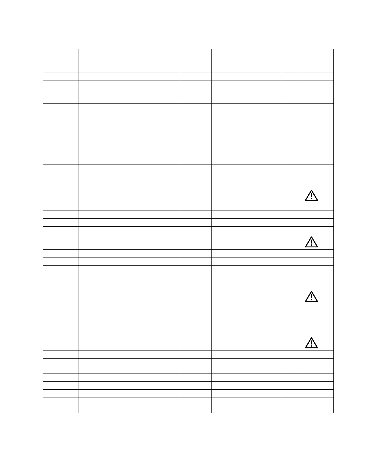
Electrical Part Lists ................................................................................................................... 10-26
Digital Signal Processor (DSP) PCB Assembly ...................................................................... 10-15
Input/Output PCB Assembly .................................................................................................... 16-20
Button and LED PCB Assembly.....................................................................................................21
Switch PCB Assembly ....................................................................................................................22
Switch Mode Power Supply (SMPS) PCB Assembly ............................................................. 23-26
Disassembly Procedures ......................................................................................................... 27-28
Test Procedures ........................................................................................................................ 29-30
Figure 4. DSP PCB Top Etch Layer and Component Layout ......................................................... 31
Figure 5. DSP PCB Internal Etch Layer 1 and Component Layout ................................................32
Figure 6. DSP PCB Internal Etch Layer 2 and Component Layout ................................................33
Figure 7. DSP PCB Bottom Etch Layer and Component Layout .................................................... 34
Figure 8. Input/Output PCB Top Etch and Component Layout ....................................................... 35
Figure 9. Input/Output PCB Bottom Etch and Component Layout .................................................35
Figure 10. Button and LED PCB Top Etch and Component Layout ...............................................36
Figure 11. Button and LED PCB Top Etch and Component Layout ...............................................36
Figure 12. Standby Switch PCB Top Etch and Component Layout ................................................36
Figure 13. Standby Switch PCB Bottom Etch and Component Layout ..........................................36
Figure 14. Switch Mode Power Supply PCB Top Etch and Component Layout .............................37
Figure 15. Switch Mode Power Supply PCB Bottom Etch and Component Layout ....................... 37
Software Update Installation Procedure ................................................................................. 38-40
Panaray Digital Controller II EQ Curves.................................................................................. 41-54
Theory of Operation .................................................................................................................. 55-57
Panaray Digital Controller II Block Diagram .................................................................................58
Integrated Circuit Diagrams ..................................................................................................... 59-61
Service Manual Revision History...................................................................................................62
1
Page 2

SAFETY INFORMATION
1. Parts that have special safety characteristics are identified by the symbol on schematics
or by special notes on the parts list. Use only replacement parts that have critical characteristics
recommended by the manufacturer.
2. Make leakage current or resistance measurements to determine that exposed parts are
acceptably insulated from the supply circuit before returning the unit to the customer.
Use the following checks to perform these measurements:
A. Leakage Current Hot Check-With the unit completely reassembled, plug the AC line cord
directly into a 120V AC outlet. (Do not use an isolation transformer during this test.) Use a
leakage current tester or a metering system that complies with American National Standards
Institute (ANSI) C101.1 "Leakage Current for Appliances" and Underwriters Laboratories (UL)
UL6500 / UL60065 / IEC 60065 paragraph 9.1.1. With the unit AC switch first in the ON position
and then in OFF position, measure from a known earth ground (metal waterpipe, conduit, etc.)
to all exposed metal parts of the unit (antennas, handle bracket, metal cabinet, screwheads,
metallic overlays, control shafts, etc.), especially any exposed metal parts that offer an electrical
return path to the chassis. Any current measured must not exceed 0.5 milliamp. Reverse the
unit power cord plug in the outlet and repeat test. ANY MEASUREMENTS NOT WITHIN THE
LIMITS SPECIFIED HEREIN INDICATE A POTENTIAL SHOCK HAZARD THAT MUST BE
ELIMINATED BEFORE RETURNING THE UNIT TO THE CUSTOMER.
B. Insulation Resistance Test Cold Check-(1) Unplug the power supply and connect a jumper
wire between the two prongs of the plug. (2) Turn on the power switch of the unit. (3) Measure
the resistance with an ohmmeter between the jumpered AC plug and each exposed metallic
cabinet part on the unit. When testing 3 wire products, the resistance measured to the product
enclosure should be between 2 and infinite MOhms. Also, the resistance measured to exposed
input/output connectors should be between 4 and infinite MOhms. When testing 2 wire products, the resistance measured to exposed input/output connectors should be between 4 and
infinite MOhms. If it is not within the limits specified, there is the possibility of a shock hazard,
and the unit must be repaired and rechecked before it is returned to the customer.
CAUTION: The Bose® Panaray® System Digital Controller II
contains no user-serviceable parts. To prevent warranty infractions,
refer servicing to warranty service stations or factory service.
PROPRIETARY INFORMATION
THIS DOCUMENT CONTAINS PROPRIETARY INFORMATION OF
BOSE CORPORATION WHICH IS BEING FURNISHED ONLY FOR
THE PURPOSE OF SERVICING THE IDENTIFIED BOSE PRODUCT
BY AN AUTHORIZED BOSE SERVICE CENTER OR OWNER OF
THE BOSE PRODUCT, AND SHALL NOT BE REPRODUCED OR
USED FOR ANY OTHER PURPOSE.
WARRANTY
The Bose Panaray System Digital Controller II is covered by a limited 1-year transferable
limited warranty. Warranty period for Europe is 2 years.
2
Page 3

Product Description
The Bose® Panaray® System Digital Controller II is the next generation of the Bose Panaray
Digital Controller. It is a 1U rack mount controller with 2 inputs and 4 outputs, and it’s primary
purpose is to provide selectable loudspeaker EQ. It utilizes a TI TMS320D707RPF digital signal
processor to provide Bose speaker equalizer curves for all current and future speaker products.
The unit’s firmware is field upgradeable via a serial port and will not support dual mono preset
operation.
The controller is a world-wide product that utilizes a switch-mode power supply, allowing it to
operate on any line voltage from 100V to 240VAC, 50/60Hz. The Controller II is also RoHS and
WEEE compliant.
The Panaray System Digital Controller II replaces the Panaray System Digital Controller.
The controller utilizes a digital signal processing (DSP) architecture to provide Bose speaker
equalizer curves for all current and future loudspeakers.
The DSP engine has the capability to run the following operations simultaneously:
- Parametric EQ: One stereo (or mono) seven band parametric equalizer capable of the
following
• Seven band parametric
• Six band parametric with high pass
• Six band parametric with low pass
• Five band parametric with a high pass and low pass
- Crossover: Two mono or a single stereo crossover
• Choice of Butterworth, Linkwitz Riley, and Bessel Filters
• These support 1st, 2nd, 3rd and 4th order slopes.
• Output Limiter: Four mono or two stereo output limiters capable of being assigned
to any of the four outputs.
- Routing: Independent routing of input program material to any of the four outputs.
- Line Delay: Delay is available only to presets located in the Bass Array bank
• None of these settings are user programmable.
• The controller has the ability to accommodate up to 180 ROM presets capable of
supporting all combinations of Bose speakers products. The speaker presets are
not editable by the end user.
3
Page 4

SPECIFICATIONS
Front Panel Controls
Standby Power ON/OFF
Input/Output LEDs Signal (present) LED - green
Range is -40dB to -3dB
1 x LEDs for CH1 and CH2
Signal (clip) LED - red
Range is 0dB
1 x LEDs for CH1 and CH2
Display 2 x 16 backlit LCD display - blue background
with white characters
Up/Down/Left/Right Buttons Navigate EQ and utility menus
Select/Load Button Selects Bose
Rear Panel Connectors
Analog Inputs Two analog, balanced, differential XLR
Analog Outputs Four analog, balanced, differential, XLR
Communication Port DB-9 serial connector, RS232 (for updates only)
IEC Power IEC power cord input
®
EQ for speakers selected
Electrical Specifications
Analog Inputs Two balanced XLR connectors, CH1 and CH2
Input Impedance, Differential 2k Ohm
Maximum Input Level +18 dBu
Sensitivity Range at Full Scale Selectable 0/+6/+12/+18 dBu
A to D Conversion 24 bit, 128x oversampling bitstream
Dynamic Range 103 dB (typical)
THD 0.003% (typical)
Frequency Response 20Hz to 20kHz, +0/-1dB
Crosstalk 100 dB (typical)
Analog Outputs Four balanced, differential XLR connectors
Output Impedance, Differential 200 Ohms
Maximum Ouput Level (balanced) +18 dBu
Output Ranges, Balanced Selectable 0/+6/+12/+18 dBu
Throughput Delay 1.52ms
Conversion 44.1kHz
Mains Voltage 100 to 240VAC, 50 to 60Hz (auto-select)
Power Consumption < 15 Watts
Environmental Operating temperature: 32 - 104 degrees F (0 - 40 C)
Storage temperature: -4 -122 degrees F (-20 - 50 C)
Humidity: 95% relative humidity
Dimensions 19”W x 8.27”D x 1.77”H (483 x 210 x 45mm)
System Weight Product: 5.9lb (2.7kg)
Shipping: 7.8lb (3.5kg)
4
Page 5

ELECTROSTATIC DISCHARGE SENSITIVE (ESDS)
DEVICE HANDLING
This unit contains ESDS devices. We recommend the following precautions when repairing,
replacing or transporting ESDS devices:
• Perform work at an electrically grounded work station.
• Wear wrist straps that connect to the station or heel straps that connect to conductive
floor mats.
• Avoid touching the leads or contacts of ESDS devices or PC boards even if properly
grounded. Handle boards by the edges only.
• Transport or store ESDS devices in ESD protective bags, bins, or totes. Do not insert
unprotected devices into materials such as plastic, polystyrene foam, clear plastic bags,
bubble wrap or plastic trays.
PART LIST NOTES
1. This part is not normally available from Customer Service. Approval from the Field Service
Manager is required before ordering.
2. The individual parts located on the PCBs are listed in the Electrical Part List.
3. This part is critical for safety purposes. Failure to use a substitute replacement with the
same safety characteristics as the recommended replacement part might create shock, fire
and/or other hazards.
4. This part is referenced for informational purposes only. It is not stocked as a repair part. Refer
to the next higher assembly for a replacement part.
5
Page 6
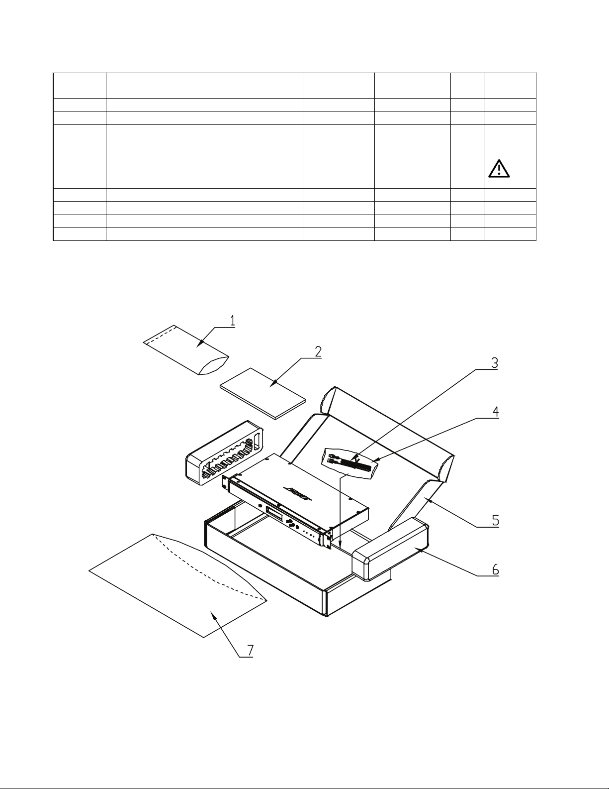
PACKAGING PART LIST
Panaray® Digital Controller II (see Figure 1)
Item
Number
1 POLYBAG 475X335X0.1 - 1497-7802+0 1
2 OWNERS MANUAL 298164 4301-7227+0 1
3 LINE CORD, 120V, US/CA 298165 7012-7340+0 1 3
LINE CORD, 230V, EURO 298166 7012-6601+0
LINE CORD, 100V, JAPAN 298167 7012-5530+0
LINE CORD, 240V, UK/SING 298168 7012-6603+0
LINE CORD, 240V, AUS 298169 7012-5430+0
4 PE BAG 350X120X0.05 - 1497-7762+0 1
5 CARTON 298162 1480-9201+1 1
6 CARTON PACKAGING 298163 1490-4621+0 1
7 POLYBAG - - 1
Description Bose® Part
Number
Vendor Part
Number
Qty. Note
Figure 1. Panaray Digital Controller II Packaging View
6
Page 7
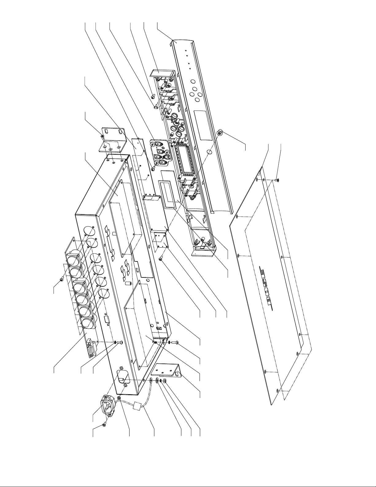
MAIN PART LIST
Panaray® System Digital Controller II (see Figure 2)
Item
Number
1 SCREW, MACHINE, CS, M3X6 - 2901-3006+3000 9 4
2 COVER, TOP 298519 1405-9901+0 1 4
- FRONT PANEL ASSEMBLY,
CONSISTS OF ITEMS 3 – 10
3 KNOB, POWER - 2447-3502+0 1 4
4 COVER, FRONT, ALUMINUM 298157 1405-9801+0 1
5 PANEL, FRONT - 1467-6801+0 1 4
6 SCREW, B-TITE, M3X8, BZ - 2954-3008+3000 5 4
7 LIGHT PIPE 298517 4155-1861+0 4
8 ARROW AND LOAD BUTTONS 298518 2447-3201+0 1
9 LENS, LCD, 72X26X1 - 3717-3006+0 1 4
10 SPONGE, LCD, 71.6X25.6X2.0 - 4149-0991+0 1 4
11 LCD DISPLAY, 3.3V, WHT
SEG/BLUE BKGND, LMB162A
12 POWER SWITCH PCB ASSY 298158 SVC-BASIC14+SW 1 2, 3
13 SCREW, B-TITE, PAN, M2.3X8 - 2950-2308+3000 13 4
14 CHASSIS - 1405-9601+0 1 4
15 SCREW, MACHINE, M3X8, BZ - 2904-3008+3000 8 4
16 SWITCH-MODE P/S, AC100-
240V, O/P, 15W
17 RACK EARS 298161 1405-9701+0 2
18 NUT, M4, BLK - 2640-4030+0703 1 4
19 WASHER, SPRING, M4X1X7 - 2607-4010+0703 1 4
20 WASHER, METAL, M4X0.8X10 - 2600-4008+1003 1 4
21 CHOKE, EARTH, TOROIDAL,
200uH, #18 WIRE, GREEN /
YELLOW
22 NUT, M3, NI - 2640-3022+0544 2 4
23 SCREW, M3X8, C'SINK, BLK - 2901-3008+3000 2 4
24 INLET, AC, UL/CSA/VDE,
250V, 10A (Rong Feng
Industrial Co., SS-7B, 250V,
10A VDE,15A UL/CSA)
25 SCREW, M3X6, BINDING, BLK - 2904-3006+3000 2 4
26 WASHER, SPRING,
M3X0.9X5.5, BZ
27 INPUT/OUTPUT PCB ASSY 298152 SVC-BASIC14+I/O 1 2
28 SCREW, 3X8, TAPPING - 2950-3008+3000 12 4
29 DSP PCB ASSY 298154 SVC-BASIC14+DSP 1 2
30 SCREW, MACHINE, CS, M3X6 - 2901-3006+3000 6 4
31 BUTTON AND LED PCB ASSY 298160 SVC-BASIC14+KEY 1 2
Description Bose®
Part
Number
299033 SVC-BASIC14+FPAN 1
298159 8902-0005+0 1
298155 8902-0009+0 1 2, 3
- 1806-3917+0 1 3, 4
298153 2113-1144+0 1 3
- 2607-3009+0553 10 4
Vendor Part Number Qty. Note
7
Page 8
6
31
30
29
5
7
8
6
4
1
3
2
28
27
26
25
24
23
22
21
13
14
15
16
17
201918
12
109
11
Figure 2. Panaray System Digital Controller II Exploded View
8
Page 9
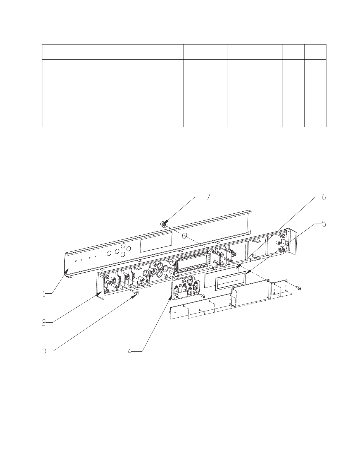
MAIN PART LIST
Front Panel Sub-assembly (see Figure 3)
Item
Number
- FRONT PANEL SUBASSEMBLY
CONSISTS OF:
1 COVER, FRONT, ALUMINUM 298157 1405-9801+0 1 4
2 PANEL, FRONT - 1467-6801+0 1 4
3 LED LIGHT PIPE 298517 4155-1861+0 4 4
4 ARROW AND LOAD BUTTONS 298518 2447-3201+0 1 4
5 SPONGE FRAME, LCD - 4149-0991+0 1 4
6 LENS, LCD - 3717-3006+0 1 4
7 BUTTON, POWER - 2447-3502+0 1 4
Description Bose® Part
Number
299033 SVC-
Vendor Part
Number
BASIC14+FPAN
Qty. Note
1
Figure 3. Front Panel Sub-assembly Exploded View
9
Page 10

ELECTRICAL PART LIST
Digital Signal Processor (DSP) PCB Assembly
Resistors
Reference
Designator
R101 33RX4, RCFA, 0603, 1/16W, 5% 4703-330J+P-04 4
R102 220RX4, RCFA, 0603, 1/16W, 5% 4703-221J+P-04 4
R103 33RX4, RCFA, 0603, 1/16W, 5% 4703-330J+P-04 4
R104 33RX4, RCFA, 0603, 1/16W, 5% 4703-330J+P-04 4
R105 33RX4, RCFA, 0603, 1/16W, 5% 4703-330J+P-04 4
R106 33RX4, RCFA, 0603, 1/16W, 5% 4703-330J+P-04 4
R107 33RX4, RCFA, 0603, 1/16W, 5% 4703-330J+P-04 4
R108 33RX4, RCFA, 0603, 1/16W, 5% 4703-330J+P-04 4
R109 33RX4, RCFA, 0603, 1/16W, 5% 4703-330J+P-04 4
R110 33RX4, RCFA, 0603, 1/16W, 5% 4703-330J+P-04 4
R111 33RX4, RCFA, 0603, 1/16W, 5% 4703-330J+P-04 4
R112 33RX4, RCFA, 0603, 1/16W, 5% 4703-330J+P-04 4
R113 33RX4, RCFA, 0603, 1/16W, 5% 4703-330J+P-04 4
R114 33RX4, RCFA, 0603, 1/16W, 5% 4703-330J+P-04 4
R115 33RX4, RCFA, 0603, 1/16W, 5% 4703-330J+P-04 4
R116 33RX4, RCFA, 0603, 1/16W, 5% 4703-330J+P-04 4
R117 33RX4, RCFA, 0603, 1/16W, 5% 4703-330J+P-04 4
R118 33RX4, RCFA, 0603, 1/16W, 5% 4703-330J+P-04 4
R119 33RX4, RCFA, 0603, 1/16W, 5% 4703-330J+P-04 4
R120 33RX4, RCFA, 0603, 1/16W, 5% 4703-330J+P-04 4
R121 10KX4, RCFA, 0603, 1/16W, 5% 4703-103J+P-04 4
R124 10KX4, RCFA, 0603, 1/16W, 5% 4703-103J+P-04 4
R125 10KX4, RCFA, 0603, 1/16W, 5% 4703-103J+P-04 4
R126 1KX4, RCFA, 0603, 1/16W, 5% 4703-102J+P-04 4
R127 220RX4, RCFA, 0603, 1/16W, 5% 4703-221J+P-04 4
R128 10KX4, RCFA, 0603, 1/16W, 5% 4703-103J+P-04 4
R129 33RX4, RCFA, 0603, 1/16W, 5% 4703-330J+P-04 4
R500 220 OHM, 0603/1608, RMG, 1/16W, 1% 4723-221A+P 4
R501 220 OHM, 0603/1608, RMG, 1/16W, 1% 4723-221A+P 4
R502 33 OHM, 0603, RMG, 1/16W, 1% 4723-330A+P 4
R503 33 OHM, 0603, RMG, 1/16W, 1% 4723-330A+P 4
R504 10K, 0603/1608, RMG, 1/16W, 1% 4723-103A+P 4
R505 10K, 0603/1608, RMG, 1/16W, 1% 4723-103A+P 4
R506 10K, 0603/1608, RMG, 1/16W, 1% 4723-103A+P 4
R507 10K, 0603/1608, RMG, 1/16W, 1% 4723-103A+P 4
R508 10K, 0603/1608, RMG, 1/16W, 1% 4723-103A+P 4
R509 10K, 0603/1608, RMG, 1/16W, 1% 4723-103A+P 4
R510 10K, 0603/1608, RMG, 1/16W, 1% 4723-103A+P 4
R511 200 OHM, 0603, RMG, 1/16W, 1% 4723-201A+P 4
R512 100 OHM, 0603, RMG, 1/16W, 1% 4723-101A+P 4
R513 10 OHM, 0603, RMG, 1/16W, 1% 4723-100A+P-R 4
R514 2.2K, 0603/1608, RMG, 1/16W, 1% 4723-222A+P 4
R515 1K, 0603/1608, RMG, 1/16W, 1% 4723-102A+P 4
R516 1K, 0603/1608, RMG, 1/16W, 1% 4723-102A+P 4
R517 1K, 0603/1608, RMG, 1/16W, 1% 4723-102A+P 4
R518 1K, 0603/1608, RMG, 1/16W, 1% 4723-102A+P 4
R519 2.2K, 0603/1608, RMG, 1/16W, 1% 4723-222A+P 4
Description Vendor Part
Number
Note
10
Page 11

ELECTRICAL PART LIST
Digital Signal Processor (DSP) PCB Assembly
Resistors (continued)
Reference
Designator
R520 1K, 0603/1608, RMG, 1/16W, 1% 4723-102A+P 4
R521 2.2K, 0603/1608, RMG, 1/16W, 1% 4723-222A+P 4
R522 1K, 0603/1608, RMG, 1/16W, 1% 4723-102A+P 4
R523 1K, 0603/1608, RMG, 1/16W, 1% 4723-102A+P 4
R524 1K, 0603/1608, RMG, 1/16W, 1% 4723-102A+P 4
R525 2.2K, 0603/1608, RMG, 1/16W, 1% 4723-222A+P 4
R526 330 OHM, 0603, RMG, 1/16W, 1% 4723-331A+P 4
R527 2.2K, 0603/1608, RMG, 1/16W, 1% 4723-222A+P 4
R528 330 OHM, 0603, RMG, 1/16W, 1% 4723-331A+P 4
R529 2.2K, 0603/1608, RMG, 1/16W, 1% 4723-222A+P 4
R530 330 OHM, 0603, RMG, 1/16W, 1% 4723-331A+P 4
R531 2.2K, 0603/1608, RMG, 1/16W, 1% 4723-222A+P 4
R532 330 OHM, 0603, RMG, 1/16W, 1% 4723-331A+P 4
R533 2.2K, 0603/1608, RMG, 1/16W, 1% 4723-222A+P 4
R534 0 OHM, 0603, RMG, 1/16W, 5% 4723-000J+P 4
R535 0 OHM, 0603, RMG, 1/16W, 5% 4723-000J+P 4
R536 0 OHM, 0603, RMG, 1/16W, 5% 4723-000J+P 4
R537 0 OHM, 0603, RMG, 1/16W, 5% 4723-000J+P 4
R538 40.2 OHM, 0603, RMG, 1/16W, 1% 4723-40R2+P 4
R539 40.2 OHM, 0603, RMG, 1/16W, 1% 4723-40R2+P 4
R540 40.2 OHM, 0603, RMG, 1/16W, 1% 4723-40R2+P 4
R541 40.2 OHM, 0603, RMG, 1/16W, 1% 4723-40R2+P 4
R542 10K, 0603/1608, RMG, 1/16W, 1% 4723-103A+P 4
R543 10K, 0603/1608, RMG, 1/16W, 1% 4723-103A+P 4
R544 10K, 0603/1608, RMG, 1/16W, 1% 4723-103A+P 4
R545 270 OHM, 0603/1608, RMG, 1/16W, 1% 4723-271A+P 4
R546 2K, 0603/1608, RMG, 1/16W, 1% 4723-202A+P 4
R547 2K, 0603/1608, RMG, 1/16W, 1% 4723-202A+P 4
R548 0 OHM, 0603, RMG, 1/16W, 5% 4723-000J+P 4
R549 0 OHM, 0603, RMG, 1/16W, 5% 4723-000J+P 4
R550 0 OHM, 0603, RMG, 1/16W, 5% 4723-000J+P 4
R551 0 OHM, 0603, RMG, 1/16W, 5% 4723-000J+P 4
R552 10K, 0603/1608, RMG, 1/16W, 1% 4723-103A+P 4
R553 1K, 0603/1608, RMG, 1/16W, 1% 4723-102A+P 4
R554 33K, 0603/1608, RMG, 1/16W, 5% 4723-333J+P 4
R555 0 OHM, 0603, RMG, 1/16W, 5% 4723-000J+P 4
R556 0 OHM, 0603, RMG, 1/16W, 5% 4723-000J+P 4
R557 10K, 0603/1608, RMG, 1/16W, 1% 4723-103A+P 4
R710 10K, 0603/1608, RMG, 1/16W, 1% 4723-103A+P 4
R810 10K, 0603/1608, RMG, 1/16W, 1% 4723-103A+P 4
R902 33 OHM, 0603, RMG, 1/16W, 1% 4723-330A+P 4
R903 220 OHM, 0603/1608, RMG, 1/16W, 1% 4723-221A+P 4
R904 220 OHM, 0603/1608, RMG, 1/16W, 1% 4723-221A+P 4
R905 220 OHM, 0603/1608, RMG, 1/16W, 1% 4723-221A+P 4
R906 220 OHM, 0603/1608, RMG, 1/16W, 1% 4723-221A+P 4
R907 150 OHM, 0603, RMG, 1/16W, 1% 4723-151A+P 4
Description Vendor Part
Number
Note
11
Page 12

ELECTRICAL PART LIST
Digital Signal Processor (DSP) PCB Assembly
Capacitors
Reference
Designator
C500 0.1uF, CC, 0603/1608, 50V, 10%, 1x2 150F-104K+P-AC 4
C501 0.1uF, CC, 0603/1608, 50V, 10%, 1x2 150F-104K+P-AC 4
C502 0.1uF, CC, 0603/1608, 50V, 10%, 1x2 150F-104K+P-AC 4
C503 0.1uF, CC, 0603/1608, 50V, 10%, 1x2 150F-104K+P-AC 4
C504 0.1uF, CC, 0603/1608, 50V, 10%, 1x2 150F-104K+P-AC 4
C505 0.1uF, CC, 0603/1608, 50V, 10%, 1x2 150F-104K+P-AC 4
C506 0.1uF, CC, 0603/1608, 50V, 10%, 1x2 150F-104K+P-AC 4
C507 0.01uF, CC, 0603, 50V, 10%, 1x2 150F-103K+P-AC 4
C508 0.01uF, CC, 0603, 50V, 10%, 1x2 150F-103K+P-AC 4
C509 0.1uF, CC, 0603/1608, 50V, 10%, 1x2 150F-104K+P-AC 4
C510 0.1uF, CC, 0603/1608, 50V, 10%, 1x2 150F-104K+P-AC 4
C511 0.1uF, CC, 0603/1608, 50V, 10%, 1x2 150F-104K+P-AC 4
C512 0.1uF, CC, 0603/1608, 50V, 10%, 1x2 150F-104K+P-AC 4
C513 0.1uF, CC, 0603/1608, 50V, 10%, 1x2 150F-104K+P-AC 4
C514 0.1uF, CC, 0603/1608, 50V, 10%, 1x2 150F-104K+P-AC 4
C515 0.1uF, CC, 0603/1608, 50V, 10%, 1x2 150F-104K+P-AC 4
C516 0.1uF, CC, 0603/1608, 50V, 10%, 1x2 150F-104K+P-AC 4
C518 0.1uF, CC, 0603/1608, 50V, 10%, 1x2 150F-104K+P-AC 4
C520 0.1uF, CC, 0603/1608, 50V, 10%, 1x2 150F-104K+P-AC 4
C521 0.1uF, CC, 0603/1608, 50V, 10%, 1x2 150F-104K+P-AC 4
C522 0.1uF, CC, 0603/1608, 50V, 10%, 1x2 150F-104K+P-AC 4
C523 0.1uF, CC, 0603/1608, 50V, 10%, 1x2 150F-104K+P-AC 4
C524 0.1uF, CC, 0603/1608, 50V, 10%, 1x2 150F-104K+P-AC 4
C525 0.1uF, CC, 0603/1608, 50V, 10%, 1x2 150F-104K+P-AC 4
C526 0.1uF, CC, 0603/1608, 50V, 10%, 1x2 150F-104K+P-AC 4
C527 0.1uF, CC, 0603/1608, 50V, 10%, 1x2 150F-104K+P-AC 4
C528 0.1uF, CC, 0603/1608, 50V, 10%, 1x2 150F-104K+P-AC 4
C529 0.1uF, CC, 0603/1608, 50V, 10%, 1x2 150F-104K+P-AC 4
C530 0.1uF, CC, 0603/1608, 50V, 10%, 1x2 150F-104K+P-AC 4
C531 0.1uF, CC, 0603/1608, 50V, 10%, 1x2 150F-104K+P-AC 4
C532 0.1uF, CC, 0603/1608, 50V, 10%, 1x2 150F-104K+P-AC 4
C533 0.1uF, CC, 0603/1608, 50V, 10%, 1x2 150F-104K+P-AC 4
C534 0.1uF, CC, 0603/1608, 50V, 10%, 1x2 150F-104K+P-AC 4
C535 0.1uF, CC, 0603/1608, 50V, 10%, 1x2 150F-104K+P-AC 4
C536 0.1uF, CC, 0603/1608, 50V, 10%, 1x2 150F-104K+P-AC 4
C537 0.1uF, CC, 0603/1608, 50V, 10%, 1x2 150F-104K+P-AC 4
C538 0.1uF, CC, 0603/1608, 50V, 10%, 1x2 150F-104K+P-AC 4
C539 0.1uF, CC, 0603/1608, 50V, 10%, 1x2 150F-104K+P-AC 4
C540 0.1uF, CC, 0603/1608, 50V, 10%, 1x2 150F-104K+P-AC 4
C541 0.1uF, CC, 0603/1608, 50V, 10%, 1x2 150F-104K+P-AC 4
C542 0.1uF, CC, 0603/1608, 50V, 10%, 1x2 150F-104K+P-AC 4
C543 0.1uF, CC, 0603/1608, 50V, 10%, 1x2 150F-104K+P-AC 4
C544 0.1uF, CC, 0603/1608, 50V, 10%, 1x2 150F-104K+P-AC 4
C545 0.1uF, CC, 0603/1608, 50V, 10%, 1x2 150F-104K+P-AC 4
C546 0.1uF, CC, 0603/1608, 50V, 10%, 1x2 150F-104K+P-AC 4
C547 0.1uF, CC, 0603/1608, 50V, 10%, 1x2 150F-104K+P-AC 4
C548 0.1uF, CC, 0603/1608, 50V, 10%, 1x2 150F-104K+P-AC 4
C549 0.1uF, CC, 0603/1608, 50V, 10%, 1x2 150F-104K+P-AC 4
Description Vendor Part
Number
Note
12
Page 13

ELECTRICAL PART LIST
Digital Signal Processor (DSP) PCB Assembly
Capacitors (continued)
Reference
Designator
C550 0.1uF, CC, 0603/1608, 50V, 10%, 1x2 150F-104K+P-AC 4
C551 0.1uF, CC, 0603/1608, 50V, 10%, 1x2 150F-104K+P-AC 4
C552 0.1uF, CC, 0603/1608, 50V, 10%, 1x2 150F-104K+P-AC 4
C553 0.1uF, CC, 0603/1608, 50V, 10%, 1x2 150F-104K+P-AC 4
C554 0.1uF, CC, 0603/1608, 50V, 10%, 1x2 150F-104K+P-AC 4
C555 0.1uF, CC, 0603/1608, 50V, 10%, 1x2 150F-104K+P-AC 4
C556 0.1uF, CC, 0603/1608, 50V, 10%, 1x2 150F-104K+P-AC 4
C557 1uF, CC, 0805, 50V, +80/-20% 150F-105Z+J-BD 4
C558 0.22uF, CC, 0603, 50V, +80/-20% 150F-224Z+P-AC 4
C559 0.22uF, CC, 0603, 50V, +80/-20% 150F-224Z+P-AC 4
C560 0.22uF, CC, 0603, 50V, +80/-20% 150F-224Z+P-AC 4
C561 0.22uF, CC, 0603, 50V, +80/-20% 150F-224Z+P-AC 4
C562 0.22uF, CC, 0603, 50V, +80/-20% 150F-224Z+P-AC 4
C563 0.22uF, CC, 0603, 50V, +80/-20% 150F-224Z+P-AC 4
C564 0.22uF, CC, 0603, 50V, +80/-20% 150F-224Z+P-AC 4
C565 0.22uF, CC, 0603, 50V, +80/-20% 150F-224Z+P-AC 4
C566 0.22uF, CC, 0603, 50V, +80/-20% 150F-224Z+P-AC 4
C567 0.22uF, CC, 0603, 50V, +80/-20% 150F-224Z+P-AC 4
C568 0.22uF, CC, 0603, 50V, +80/-20% 150F-224Z+P-AC 4
C569 0.22uF, CC, 0603, 50V, +80/-20% 150F-224Z+P-AC 4
C570 0.22uF, CC, 0603, 50V, +80/-20% 150F-224Z+P-AC 4
C571 0.22uF, CC, 0603, 50V, +80/-20% 150F-224Z+P-AC 4
C572 0.1uF, CC, 0603/1608, 50V, 10%, 1x2 150F-104K+P-AC 4
C573 1000pF, CC, 0603/1608, 50V, 10%, 1X2 150F-102K+P-AC 4
C574 1000pF, CC, 0603/1608, 50V, 10%, 1X2 150F-102K+P-AC 4
C575 1000pF, CC, 0603/1608, 50V, 10%, 1X2 150F-102K+P-AC 4
C576 1000pF, CC, 0603/1608, 50V, 10%, 1X2 150F-102K+P-AC 4
C577 1000pF, CC, 0603/1608, 50V, 10%, 1X2 150F-102K+P-AC 4
C578 1000pF, CC, 0603/1608, 50V, 10%, 1X2 150F-102K+P-AC 4
C579 1000pF, CC, 0603/1608, 50V, 10%, 1X2 150F-102K+P-AC 4
C580 1000pF, CC, 0603/1608, 50V, 10%, 1X2 150F-102K+P-AC 4
C583 2700pF, CC, 0603/1608, 50V, 10% 150F-272K+P-AC 4
C584 2700pF, CC, 0603/1608, 50V, 10% 150F-272K+P-AC 4
C748 0.1uF, CC, 0603/1608, 50V, 10%, 1x2 150F-104K+P-AC 4
C749 0.01uF, CC, 0603, 50V, 10%, 1x2 150F-103K+P-AC 4
C750 0.1uF, CC, 0603/1608, 50V, 10%, 1x2 150F-104K+P-AC 4
C751 0.01uF, CC, 0603, 50V, 10%, 1x2 150F-103K+P-AC 4
C752 0.1uF, CC, 0603/1608, 50V, 10%, 1x2 150F-104K+P-AC 4
CT500 10uF, SM, CE, 16V, 20%, 4X5.4, PSI, VS 157D-106M+3-GJK 4
CT501 10uF, SMD, CT, 16V, 20%, 1.6X3.2 154D-106M+3-CF 4
CT502 10uF, SMD, CT, 16V, 20%, 1.6X3.2 154D-106M+3-CF 4
CT503 10uF, SMD, CT, 16V, 20%, 1.6X3.2 154D-106M+3-CF 4
CT504 10uF, SMD, CT, 16V, 20%, 1.6X3.2 154D-106M+3-CF 4
CT505 10uF, SMD, CT, 16V, 20%, 1.6X3.2 154D-106M+3-CF 4
CT506 10uF, SMD, CT, 16V, 20%, 1.6X3.2 154D-106M+3-CF 4
CT507 10uF, SMD, CT, 16V, 20%, 1.6X3.2 154D-106M+3-CF 4
CT508 10uF, SM, CE, 16V, 20%, 4X5.4, PSI, VS 157D-106M+3-GJK 4
CT509 10uF, SM, CE, 16V, 20%, 4X5.4, PSI, VS 157D-106M+3-GJK 4
Description Vendor Part
Number
Note
13
Page 14
ELECTRICAL PART LIST
Digital Signal Processor (DSP) PCB Assembly
Capacitors (continued)
Reference
Designator
CT510 10uF, SMD, CT, 16V, 20%, 1.6X3.2 154D-106M+3-CF 4
CT511 10uF, SMD, CT, 16V, 20%, 1.6X3.2 154D-106M+3-CF 4
CT512 10uF, SM, CT, 25V, 20%, 3.2x6 154E-106M+3-FK 4
CT513 10uF, SMD, CT, 16V, 20%, 1.6X3.2 154D-106M+3-CF 4
CT514 10uF, SMD, CT, 16V, 20%, 1.6X3.2 154D-106M+3-CF 4
CT515 10uF, SMD, CT, 16V, 20%, 1.6X3.2 154D-106M+3-CF 4
CT516 10uF, SMD, CT, 16V, 20%, 1.6X3.2 154D-106M+3-CF 4
CT517 10uF, SM, CT, 25V, 20%, 3.2x6 154E-106M+3-FK 4
CT518 10uF, SMD, CT, 16V, 20%, 1.6X3.2 154D-106M+3-CF 4
CT519 10uF, SMD, CT, 16V, 20%, 1.6X3.2 154D-106M+3-CF 4
CT521 10uF, SM, CT, 25V, 20%, 3.2x6 154E-106M+3-FK 4
CT522 10uF, SM, CT, 25V, 20%, 3.2x6 154E-106M+3-FK 4
CT531 10uF, SMD, CT, 16V, 20%, 1.6X3.2 154D-106M+3-CF 4
CT532 10uF, SMD, CT, 16V, 20%, 1.6X3.2 154D-106M+3-CF 4
CT533 1uF, SM, CT, 16V, 20%, 1.6X3.2 154D-105M+3-CF 4
CT534 1uF, SM, CT, 16V, 20%, 1.6X3.2 154D-105M+3-CF 4
CT535 10uF, SM, CE, 16V, 20%, 4X5.4, PSI, VS 157D-106M+3-GJK 4
CT720 10uF, SMD, CT, 16V, 20%, 1.6X3.2 154D-106M+3-CF 4
Reference
Designator
L500 EMI FILTER, FERRITE, CHIP, EXCCET103U, SMD,
PANASONIC
L501 INDUCTOR, CHIP, 10uH, LEMF3225T100K 1803-0055+0 4
L502 INDUCTOR, CHIP, 10uH, LEMF3225T100K 1803-0055+0 4
FB500 FERRITE BEAD, SEBW201209U121MT, 0805 1808-0872+0 4
FB501 FERRITE BEAD, 4.5X1.6X1.6, BLM41PG102SN1L 1808-0871+0 4
FB505 FERRITE BEAD, 4.5X1.6X1.6, BLM41PG102SN1L 1808-0871+0 4
Description Vendor Part
Number
Note
Inductors and Ferrite Beads
Description Vendor Part
Number
2705-0020+0 4
Note
Diodes
Reference
Designator
D500 BAV99, SOT23, PHILIPS 4840-8970+3 4
D501 BAV99, SOT23, PHILIPS 4840-8970+3 4
D502 BAV99, SOT23, PHILIPS 4840-8970+3 4
D503 BAV99, SOT23, PHILIPS 4840-8970+3 4
Description Vendor Part
Number
Note
14
Page 15
ELECTRICAL PART LIST
Digital Signal Processor (DSP) PCB Assembly
Transistors
Reference
Designator
Q500 RN2402,(T5L/F/T), SMD2214530R2, TOSHIBA 4852-4020+3 4
Q501 RN2402,(T5L/F/T), SMD2214530R2, TOSHIBA 4852-4020+3 4
Q502 NPN, RN1402,(T5L/F/T), SMD, TOSHIBA,
2214470R2
Q503 NPN, RN1402,(T5L/F/T), SMD, TOSHIBA,
2214470R2
Q504 NPN, RN1402,(T5L/F/T), SMD, TOSHIBA,
2214470R2
Q505 NPN, RN1402,(T5L/F/T), SMD, TOSHIBA,
2214470R2
Reference
Designator
U500 4M FLASH, S29AL004D-90TFI02, STANDARD,
TSOP48
U501 DSP, TMS320D707RFP/S, PQFP144, TI 3132-3381+0 4
U502 PLD, EPM3064A-10, TQPF44, ALTERA 3132-3331+0 4
U503 SUPPLY VOLTAGE SUPERVISOR, TL7705BCD,
SOP-8, TI
U504 LOW-DROP LINEAR REGULATOR,
TPS726126DCQ, SOT223-5, TI
U505 SN74LV245ADWR, OCTAL B TRANSCEIVER,
SOT163-1/SO
U507 OCTAL BUFFER, SMD, SN74LVC541ADWR, TI 3132-3341+0 4
U508 24BIT DAC W/VOL, CTRL, 20P, CS4392-KZZ,
TSSOP
U509 24BIT DAC W/VOL CTRL, 20P, CS4392-KZZ,
TSSOP
U511 NJM5532M-#ZZZB, DUAL OP AMP 3131-4850+0 4
U512 STEREO A/D CONVERTER, PCM1804DB, 24BIT,
SSOP28
U513 LC2MOS, 5 OHM, RON, SPST, SW, ADG452BRZ,
SOIC16, ADI
U514 LC2MOS, 5 OHM, RON, SPST, SW, ADG452BRZ,
SOIC16, ADI
U515 AUDIO OP AMP, OPA1632D, SO-8, TI 3132-3321+0 4
U516 AUDIO OP AMP, OPA1632D, SO-8, TI 3132-3321+0 4
Description Vendor Part
Number
4851-4020+3 4
4851-4020+3 4
4851-4020+3 4
4851-4020+3 4
Note
Integrated Circuits
Description Vendor Part
Number
3132-3571+0 4
3132-3401+0 4
3132-3391+0 4
3132-0680+0 4
3132-0730+0 4
3132-0730+0 4
3132-3311+0 4
3132-3361+0 4
3132-3361+0 4
Note
Miscellaneous
Reference
Designator
Y500 CRYSTAL, 22.5792MHZ +/-50 PPM, 3.3V, 7X5X1.8,
SMD7050
J500 HEADER, 2X5P, P2.54, ST, MALE 2101-3121+0 4
CON500 2P, ST,.WAFER, P=2.5 2102-021S+004 4
CN500 HEADER, IDC, 24P, 2XP2.54, 3510 SERIES 2101-3123+0 4
CN501 WIRE-CONN, 8P, P2.5, #26, UL1007, L=260, F/M 7012-7651+0 4
CN502 HEADER, IDC, 30P, 2XP2.54, 3510 SERIES 2101-3122+0 4
Description Vendor Part
Number
2300-3279+0 4
Note
15
Page 16

ELECTRICAL PART LIST
Input/Output PCB Assembly
Resistors
Reference
Designator
R316 0 OHM, RMG, 0603, 1/16W, 5% 4723-000J+P 4
R317 0 OHM, RMG, 0603, 1/16W, 5% 4723-000J+P 4
R318 10 OHM, RMG, 0603/1608, 1/16W, 5% 4723-100J+P 4
R601 100 OHM, RMG, 0603, 1/16W, 1% 4723-101A+P 4
R602 100 OHM, RMG, 0603, 1/16W, 1% 4723-101A+P 4
R612 100 OHM, RMG, 0603, 1/16W, 1% 4723-101A+P 4
R613 100 OHM, RMG, 0603, 1/16W, 1% 4723-101A+P 4
R701 330 OHM, RMG, 0603, 1/16W, 1% 4723-331A+P 4
R702 330 OHM, RMG, 0603, 1/16W, 1% 4723-331A+P 4
R703 499 OHM, RMG, 0603, 1/16W, 1% 4723-4990+P 4
R704 499 OHM, RMG, 0603, 1/16W, 1% 4723-4990+P 4
R705 2K, RMG, 0603/1608, 1/16W, 1% 4723-202A+P 4
R706 2K, RMG, 0603/1608, 1/16W, 1% 4723-202A+P 4
R707 51 OHM, RMG, 0603, 1/16W, 1% 4723-510A+P 4
R708 51 OHM, RMG, 0603, 1/16W, 1% 4723-510A+P 4
R709 330 OHM, RMG, 0603, 1/16W, 1% 4723-331A+P 4
R710 330 OHM, RMG, 0603, 1/16W, 1% 4723-331A+P 4
R711 499 OHM, RMG, 0603, 1/16W, 1% 4723-4990+P 4
R712 499 OHM, RMG, 0603, 1/16W, 1% 4723-4990+P 4
R713 2K, RMG, 0603/1608, 1/16W, 1% 4723-202A+P 4
R714 2K, RMG, 0603/1608, 1/16W, 1% 4723-202A+P 4
R715 51 OHM, RMG, 0603, 1/16W, 1% 4723-510A+P 4
R716 51 OHM, RMG, 0603, 1/16W, 1% 4723-510A+P 4
R717 330 OHM, RMG, 0603, 1/16W, 1% 4723-331A+P 4
R718 330 OHM, RMG, 0603, 1/16W, 1% 4723-331A+P 4
R719 499 OHM, RMG, 0603, 1/16W, 1% 4723-4990+P 4
R720 499 OHM, RMG, 0603, 1/16W, 1% 4723-4990+P 4
R721 2K, RMG, 0603/1608, 1/16W, 1% 4723-202A+P 4
R722 2K, RMG, 0603/1608, 1/16W, 1% 4723-202A+P 4
R723 51 OHM, RMG, 0603, 1/16W, 1% 4723-510A+P 4
R724 51 OHM, RMG, 0603, 1/16W, 1% 4723-510A+P 4
R725 330 OHM, RMG, 0603, 1/16W, 1% 4723-331A+P 4
R726 330 OHM, RMG, 0603, 1/16W, 1% 4723-331A+P 4
R727 499 OHM, RMG, 0603, 1/16W, 1% 4723-4990+P 4
R728 499 OHM, RMG, 0603, 1/16W, 1% 4723-4990+P 4
R729 2K, RMG, 0603/1608, 1/16W, 1% 4723-202A+P 4
R730 2K, RMG, 0603/1608, 1/16W, 1% 4723-202A+P 4
R731 51 OHM, RMG, 0603, 1/16W, 1% 4723-510A+P 4
R732 51 OHM, RMG, 0603, 1/16W, 1% 4723-510A+P 4
R733 1K, RMG, 0603/1608, 1/16W, 1% 4723-102A+P 4
R734 1K, RMG, 0603/1608, 1/16W, 1% 4723-102A+P 4
R735 1K, RMG, 0603/1608, 1/16W, 1% 4723-102A+P 4
R736 1K, RMG, 0603/1608, 1/16W, 1% 4723-102A+P 4
R737 1K, RMG, 0603/1608, 1/16W, 1% 4723-102A+P 4
R738 1K, RMG, 0603/1608, 1/16W, 1% 4723-102A+P 4
R739 1K, RMG, 0603/1608, 1/16W, 1% 4723-102A+P 4
R740 1K, RMG, 0603/1608, 1/16W, 1% 4723-102A+P 4
R751N 8.2K, RMG, 0603/1608, 1/16W, 1% 4723-822A+P 4
Description Vendor Part
Number
Note
16
Page 17

ELECTRICAL PART LIST
Input/Output PCB Assembly
Resistors (continued)
Reference
Designator
R752N 10K, RMG, 0603/1608, 1/16W, 1% 4723-103A+P 4
R753N 10K, RMG, 0603/1608, 1/16W, 1% 4723-103A+P 4
R758N 10K, RMG, 0603/1608, 1/16W, 1% 4723-103A+P 4
R780 10K, RMG, 0603/1608, 1/16W, 1% 4723-103A+P 4
R782 2K, RMG, 0603/1608, 1/16W, 1% 4723-202A+P 4
R783 10K, RMG, 0603/1608, 1/16W, 1% 4723-103A+P 4
R784 2K, RMG, 0603/1608, 1/16W, 1% 4723-202A+P 4
R785 2.7K, RMG, 0603/1608, 1/16W, 5% 4723-272J+P 4
R786 2.7K, RMG, 0603/1608, 1/16W, 5% 4723-272J+P 4
R789 10K, RMG, 0603/1608, 1/16W, 1% 4723-103A+P 4
R790 2.7K, RMG, 0603/1608, 1/16W, 5% 4723-272J+P 4
R800 10 OHM, RMG, 0603/1608, 1/16W, 5% 4723-100J+P 4
R801 10 OHM, RMG, 0603/1608, 1/16W, 5% 4723-100J+P 4
R802 10 OHM, RMG, 0603/1608, 1/16W, 5% 4723-100J+P 4
R803 10 OHM, RMG, 0603/1608, 1/16W, 5% 4723-100J+P 4
R812 51 OHM, RMG, 0603, 1/16W, 1% 4723-510A+P 4
R813 51 OHM, RMG, 0603, 1/16W, 1% 4723-510A+P 4
R814 51 OHM, RMG, 0603, 1/16W, 1% 4723-510A+P 4
R815 51 OHM, RMG, 0603, 1/16W, 1% 4723-510A+P 4
R816 51 OHM, RMG, 0603, 1/16W, 1% 4723-510A+P 4
R817 51 OHM, RMG, 0603, 1/16W, 1% 4723-510A+P 4
R818 51 OHM, RMG, 0603, 1/16W, 1% 4723-510A+P 4
R819 51 OHM, RMG, 0603, 1/16W, 1% 4723-510A+P 4
Description Vendor Part
Number
Note
Capacitors
Reference
Designator
C210 0.047uF, CC, 0603, 16V, 10%, 0.8x1.6 150D-473K+P-AC 4
C211 0.1uF, CC, 0603/1608, 50V, 10%, 1x2 150F-104K+P-AC 4
C212 0.33uF, CC, 0603, 16V, 10% 150D-334K+P-AC 4
C213 0.33uF, CC, 0603, 16V, 10% 150D-334K+P-AC 4
C214 0.33uF, CC, 0603, 16V, 10% 150D-334K+P-AC 4
C312 1000pF, CC, 0603/1608, 50V, 10%, 1X2 150F-102K+P-AC 4
C313 1000pF, CC, 0603/1608, 50V, 10%, 1X2 150F-102K+P-AC 4
C314 1000pF, CC, 0603/1608, 50V, 10%, 1X2 150F-102K+P-AC 4
C315 1000pF, CC, 0603/1608, 50V, 10%, 1X2 150F-102K+P-AC 4
C316 1000pF, CC, 0603/1608, 50V, 10%, 1X2 150F-102K+P-AC 4
C317 1000pF, CC, 0603/1608, 50V, 10%, 1X2 150F-102K+P-AC 4
C318 1000pF, CC, 0603/1608, 50V, 10%, 1X2 150F-102K+P-AC 4
C319 1000pF, CC, 0603/1608, 50V, 10%, 1X2 150F-102K+P-AC 4
C701 2700pF, CC, 0603/1608, 50V, 10% 150F-272K+P-AC 4
C702 560pF, CC, 0603/1608, 50V, 10%, 1X2 150F-561K+P-AC 4
C703 0.1uF, CC, 0603/1608, 50V, 10%, 1x2 150F-104K+P-AC 4
C704 0.1uF, CC, 0603/1608, 50V, 10%, 1x2 150F-104K+P-AC 4
C705 560pF, CC, 0603/1608, 50V, 10%, 1X2 150F-561K+P-AC 4
C706 0.01uF, CC, 0603, 50V, 10%, 1x2 150F-103K+P-AC 4
C707 0.01uF, CC, 0603, 50V, 10%, 1x2 150F-103K+P-AC 4
C708 2700pF, CC, 0603/1608, 50V, 10% 150F-272K+P-AC 4
Description Vendor Part
Number
Note
17
Page 18

ELECTRICAL PART LIST
Input/Output PCB Assembly
Capacitors (continued)
Reference
Designator
C709 560pF, CC, 0603/1608, 50V, 10%, 1X2 150F-561K+P-AC 4
C710 0.1uF, CC, 0603/1608, 50V, 10%, 1x2 150F-104K+P-AC 4
C711 0.1uF, CC, 0603/1608, 50V, 10%, 1x2 150F-104K+P-AC 4
C712 560pF, CC, 0603/1608, 50V, 10%, 1X2 150F-561K+P-AC 4
C713 0.01uF, CC, 0603, 50V, 10%, 1x2 150F-103K+P-AC 4
C714 0.01uF, CC, 0603, 50V, 10%, 1x2 150F-103K+P-AC 4
C715 2700pF, CC, 0603/1608, 50V, 10% 150F-272K+P-AC 4
C716 560pF, CC, 0603/1608, 50V, 10%, 1X2 150F-561K+P-AC 4
C717 0.1uF, CC, 0603/1608, 50V, 10%, 1x2 150F-104K+P-AC 4
C718 0.1uF, CC, 0603/1608, 50V, 10%, 1x2 150F-104K+P-AC 4
C719 560pF, CC, 0603/1608, 50V, 10%, 1X2 150F-561K+P-AC 4
C720 0.01uF, CC, 0603, 50V, 10%, 1x2 150F-103K+P-AC 4
C721 0.01uF, CC, 0603, 50V, 10%, 1x2 150F-103K+P-AC 4
C722 2700pF, CC, 0603/1608, 50V, 10% 150F-272K+P-AC 4
C723 560pF, CC, 0603/1608, 50V, 10%, 1X2 150F-561K+P-AC 4
C724 0.1uF, CC, 0603/1608, 50V, 10%, 1x2 150F-104K+P-AC 4
C725 0.1uF, CC, 0603/1608, 50V, 10%, 1x2 150F-104K+P-AC 4
C726 560pF, CC, 0603/1608, 50V, 10%, 1X2 150F-561K+P-AC 4
C727 0.01uF, CC, 0603, 50V, 10%, 1x2 150F-103K+P-AC 4
C728 0.01uF, CC, 0603, 50V, 10%, 1x2 150F-103K+P-AC 4
C729 0.1uF, CC, 0603/1608, 50V, 10%, 1x2 150F-104K+P-AC 4
C730 0.1uF, CC, 0603/1608, 50V, 10%, 1x2 150F-104K+P-AC 4
C731 0.1uF, CC, 0603/1608, 50V, 10%, 1x2 150F-104K+P-AC 4
C732 0.1uF, CC, 0603/1608, 50V, 10%, 1x2 150F-104K+P-AC 4
C733 0.1uF, CC, 0603/1608, 50V, 10%, 1x2 150F-104K+P-AC 4
C734 0.1uF, CC, 0603/1608, 50V, 10%, 1x2 150F-104K+P-AC 4
C743 0.1uF, CC, 0603/1608, 50V, 10%, 1x2 150F-104K+P-AC 4
C744 0.1uF, CC, 0603/1608, 50V, 10%, 1x2 150F-104K+P-AC 4
C745 0.1uF, CC, 0603/1608, 50V, 10%, 1x2 150F-104K+P-AC 4
C746 0.01uF, CC, 0603, 50V, 10%, 1x2 150F-103K+P-AC 4
C747 0.01uF, CC, 0603, 50V, 10%, 1x2 150F-103K+P-AC 4
C748 0.01uF, CC, 0603, 50V, 10%, 1x2 150F-103K+P-AC 4
CE215 100uF, CE, 25V, 20%, GS, RLT, 6.3X11, JAM/MAN 157E-107M+K-LUG 4
CT501 100uF, CE, 25V, 20%, 5X11, RLT, RUBYCON, YK 157E-107M+K-IUY 4
CT502 100uF, CE, 25V, 20%, 5X11, RLT, RUBYCON, YK 157E-107M+K-IUY 4
CT503 100uF, CE, 25V, 20%, 5X11, RLT, RUBYCON, YK 157E-107M+K-IUY 4
CT504 100uF, CE, 25V, 20%, 5X11, RLT, RUBYCON, YK 157E-107M+K-IUY 4
CT505 100uF, CE, 25V, 20%, 5X11, RLT, RUBYCON, YK 157E-107M+K-IUY 4
CT506 100uF, CE, 25V, 20%, 5X11, RLT, RUBYCON, YK 157E-107M+K-IUY 4
CT507 100uF, CE, 25V, 20%, 5X11, RLT, RUBYCON, YK 157E-107M+K-IUY 4
CT508 100uF, CE, 25V, 20%, 5X11, RLT, RUBYCON, YK 157E-107M+K-IUY 4
CT701 10uF, CT, 25V, 20%, 3.2x6, SM 154E-106M+3-FK 4
CT702 10uF, CT, 25V, 20%, 3.2x6, SM 154E-106M+3-FK 4
CT703 10uF, CT, 25V, 20%, 3.2x6, SM 154E-106M+3-FK 4
CT704 10uF, CT, 25V, 20%, 3.2x6, SM 154E-106M+3-FK 4
CT705 10uF, CT, 25V, 20%, 3.2x6, SM 154E-106M+3-FK 4
CT706 10uF, CT, 25V, 20%, 3.2x6, SM 154E-106M+3-FK 4
Description Vendor Part
Number
Note
18
Page 19
ELECTRICAL PART LIST
Input/Output PCB Assembly
Capacitors (continued)
Reference
Designator
CT707 10uF, CT, 25V, 20%, 3.2x6, SM 154E-106M+3-FK 4
CT708 10uF, CT, 25V, 20%, 3.2x6, SM 154E-106M+3-FK 4
CT717 100uF, CE, 25V, 20%, GS, RLT, 6.3X11, JAM/MAN 157E-107M+K-LUG 4
CT718 100uF, CE, 25V, 20%, GS, RLT, 6.3X11, JAM/MAN 157E-107M+K-LUG 4
CT719 100uF, CE, 25V, 20%, GS, RLT, 6.3X11, JAM/MAN 157E-107M+K-LUG 4
Reference
Designator
L701 FERRITE BEAD INDUCTOR, BL01RN1A1F1J 1808-0680+0 4
L702 FERRITE BEAD INDUCTOR, BL01RN1A1F1J 1808-0680+0 4
L703 FERRITE BEAD INDUCTOR, BL01RN1A1F1J 1808-0680+0 4
FB701 WIRE JUMPER, ROLLER FORM, D=0.6MM 635N-0002+0 4
FB702 WIRE JUMPER, ROLLER FORM, D=0.6MM 635N-0002+0 4
FB703 WIRE JUMPER, ROLLER FORM, D=0.6MM 635N-0002+0 4
FB704 WIRE JUMPER, ROLLER FORM, D=0.6MM 635N-0002+0 4
Reference
Designator
D601 BAV99, SOT23, PHILIPS 4840-8970+3 4
D602 BAV99, SOT23, PHILIPS 4840-8970+3 4
D603 BAV99, SOT23, PHILIPS 4840-8970+3 4
D604 BAV99, SOT23, PHILIPS 4840-8970+3 4
D701 BAV99, SOT23, PHILIPS 4840-8970+3 4
D702 BAV99, SOT23, PHILIPS 4840-8970+3 4
D703 BAV99, SOT23, PHILIPS 4840-8970+3 4
D704 BAV99, SOT23, PHILIPS 4840-8970+3 4
D705 BAV99, SOT23, PHILIPS 4840-8970+3 4
D706 BAV99, SOT23, PHILIPS 4840-8970+3 4
D707 BAV99, SOT23, PHILIPS 4840-8970+3 4
D708 BAV99, SOT23, PHILIPS 4840-8970+3 4
D800 LL4148, SM 4804-1480+3 4
D801 LL4148, SM 4804-1480+3 4
D802 LL4148, SM 4804-1480+3 4
D803 LL4148, SM 4804-1480+3 4
Description Vendor Part
Number
Note
Inductors and Ferrite Beads
Description Vendor Part
Number
Note
Diodes
Description Vendor Part
Number
Note
19
Page 20
ELECTRICAL PART LIST
Input/Output PCB Assembly
Transistors
Reference
Designator
Q701N MOSFET, N-CHANNEL, 2N7002MTF, SOT-23 4902-MTF0+3 4
Q702N MOSFET, N-CHANNEL, 2N7002MTF, SOT-23 4902-MTF0+3 4
Q704 MPSA06, VCE, 80V, NS, RLT 4860-8890+K 4
Q705 MPS, A56, VCE, 80V, NS, RLT 4860-8910+K 4
Q706 MPSA06, VCE, 80V, NS, RLT 4860-8890+K 4
Q707 MPS, A56, VCE, 80V, NS, RLT 4860-8910+K 4
Q708 MPSA06, VCE, 80V, NS, RLT 4860-8890+K 4
Q709N MOSFET, N-CHANNEL, 2N7002MTF, SOT-23 4902-MTF0+3 4
Q800 MOSFET, N-CHANNEL, 2N7002MTF, SOT-23 4902-MTF0+3 4
Q801 MOSFET, N-CHANNEL, 2N7002MTF, SOT-23 4902-MTF0+3 4
Q802 MOSFET, N-CHANNEL, 2N7002MTF, SOT-23 4902-MTF0+3 4
Q803 MOSFET, N-CHANNEL, 2N7002MTF, SOT-23 4902-MTF0+3 4
Q804 MPSA06, VCE, 80V, NS, RLT 4860-8890+K 4
Q805 MPS, A56, VCE, 80V, NS, RLT 4860-8910+K 4
Reference
Designator
U202 MAX3232ECWE+, RS232, TX, SO16, MAXIM 3132-2521+0 4
U701 NJM2068M-#ZZZB, DUAL OP AMP 3130-6890+0 4
U702 NJM2068M-#ZZZB, DUAL OP AMP 3130-6890+0 4
U703 NJM2068M-#ZZZB, DUAL OP AMP 3130-6890+0 4
U704 NJM2068M-#ZZZB, DUAL OP AMP 3130-6890+0 4
Description Vendor Part
Number
Note
Integrated Circuits
Description Vendor Part
Number
Note
Miscellaneous
Reference
Designator
K1 RELAY, 2P2T, 12V, 140MM, A-12W-K, TAKAMISAWA 4500-0490+0 4
K2 RELAY, 2P2T, 12V, 140MM, A-12W-K, TAKAMISAWA 4500-0490+0 4
K3 RELAY, 2P2T, 12V, 140MM, A-12W-K, TAKAMISAWA 4500-0490+0 4
K4 RELAY, 2P2T, 12V, 140MM, A-12W-K, TAKAMISAWA 4500-0490+0 4
J202 WIRE-CONN, 2P, P2.5, #26, UL1007, L=300, F/M 7012-7541+0 4
J601 SOCKET, XLR, 3P, FEMALE, AC3FAH2-AU, AMP 2113-3158+0 4
J602 SOCKET, XLR, 3P, FEMALE, AC3FAH2-AU, AMP 2113-3158+0 4
J701 SOCKET, XLR, 3P, FEMALE, AC3FAH2-AU, AMP 2113-3159+0 4
J702 SOCKET, XLR, 3P, FEMALE, AC3FAH2-AU, AMP 2113-3159+0 4
J703 SOCKET, XLR, 3P, FEMALE, AC3FAH2-AU, AMP 2113-3159+0 4
J704 SOCKET, XLR, 3P, FEMALE, AC3FAH2-AU, AMP 2113-3159+0 4
J705 HEADER, IDC, 30P, 2XP2.54, 3510 SERIES 2101-3122+0 4
J706 WIRE-CONN, 6P, P2.5, #26, UL1007, L=150, F/M 7012-7550+0 4
J707 2P, ST. WAFER, P=2.5, COULOMB 2102-021S+004 4
JP601 WAFER, 2 PIN, P=2.54, ST, 6MM 2101-1494+0 4
JP602 WAFER, 2 PIN, P=2.54, ST, 6MM 2101-1494+0 4
P301 SOCKET, DB9, D SUB, RA, FEMALE 2113-1749+0 4
Description Vendor Part
Number
Note
20
Page 21

ELECTRICAL PART LIST
Button and LED PCB Assembly
Resistors
Reference
Designator
R0 100 OHM, RCF, 1W, 5%, AL 4708-101J+1 4
R101 470 OHM, 0603/1608, RMG, 1/16W, 1% 4723-471A+P 4
R102 910 OHM, 0603/1608, RMG, 1/16W, 1% 4723-911A+P 4
R103 470 OHM, 0603/1608, RMG, 1/16W, 1% 4723-471A+P 4
R104 910 OHM, 0603/1608, RMG, 1/16W, 1% 4723-911A+P 4
R105 10K, 0603/1608, RMG, 1/16W, 1% 4723-103A+P 4
R106 10K, 0603/1608, RMG, 1/16W, 1% 4723-103A+P 4
R107 10K, 0603/1608, RMG, 1/16W, 1% 4723-103A+P 4
R108 10K, 0603/1608, RMG, 1/16W, 1% 4723-103A+P 4
R109 10K, 0603/1608, RMG, 1/16W, 1% 4723-103A+P 4
R112 0 OHM, 0603, RMG, 1/16W, 5% 4723-000J+P 4
R113 0 OHM, 0603, RMG, 1/16W, 5% 4723-000J+P 4
R115 0 OHM, 0603, RMG, 1/16W, 5% 4723-000J+P 4
Reference
Designator
C102 100uF, CE, 16V, 20%, RLT, 5X11, SHOEI 157D-107M+K-IUI 4
C105 0.1uF, CC, 0603/1608, 50V, 10%, 1x2 150F-104K+P-AC 4
Description Vendor Part
Number
Note
Capacitors
Description Vendor Part
Number
Note
Diodes
Reference
Designator
D101 SIL, 3144D, GREEN LED, 3MM 3700-9509+0 4
D103 SIL, 3144D, GREEN LED, 3MM 3700-9509+0 4
D102 LED, SIL-3143D, 3MM, RED 3700-9516+0 4
D104 LED, SIL-3143D, 3MM, RED 3700-9516+0 4
Reference
Designator
Q101 NPN, RN1402,(T5L/F/T), SMD, TOSHIBA, 2214470R2 4851-4020+3 4
Q102 RN2402,(T5L/F/T), SMD2214530R2, TOSHIBA 4852-4020+3 4
Reference
Designator
SW101 SW, TACT, SPST, SKQNAED010, H=5, ALPS 5200-4847+0-01 4
SW102 SW, TACT, SPST, SKQNAED010, H=5, ALPS 5200-4847+0-01 4
SW103 SW, TACT, SPST, SKQNAED010, H=5, ALPS 5200-4847+0-01 4
SW104 SW, TACT, SPST, SKQNAED010, H=5, ALPS 5200-4847+0-01 4
SW105 SW, TACT, SPST, SKQNAED010, H=5, ALPS 5200-4847+0-01 4
J301 WIRE-CONN, 2P, P2.5, #26, UL1007, L=150, RD/BK,
F/M
J302 HEADER, IDC, 24P, 2XP2.54, 3510 SERIES 2101-3123+0 4
J303 16P, ST, WAFER, P=2.0 2102-160S+003 4
Description Vendor Part
Number
Note
Transistors
Description Vendor Part
Number
Note
Miscellaneous
Description Vendor Part
Number
7012-7542+0 4
Note
21
Page 22

ELECTRICAL PART LIST
Switch PCB Assembly
Resistors
Reference
Designator
R910 30K, RMG, 0603/1608, 1/16W, 1% 4723-303A+P 4
R911 1K, RMG, 0603/1608, 1/16W, 1% 4723-102A+P 4
R912 10 OHM, RMG, 0603/1608, 1/16W, 1% 4723-100A+P 4
R913 1K, RMG, 0603/1608, 1/16W, 1% 4723-102A+P 4
Reference
Designator
C572 0.1uF, CC, 0603/1608, 50V, 10%, 1x2 150F-104K+P-AC 4
CT102 10uF, CT, SMD, 16V, 20%, 1.6X3.2 154D-106M+3-CF 4
Reference
Designator
Q503 NPN, RN1402,(T5L/F/T), SMD, TOSHIBA, 2214470R2 4851-4020+3 4
Q702N MOSFET, N-CHANNEL, 2N7002MTF, SOT-23 4902-MTF0+3 4
Reference
Designator
SW106 SW, PUSH, 2P2T, L=9.6, SFPC12MA02-GK 5200-4920+0-11 4
J104 WIRE-CONN, 2P, P2.5, #26, UL1007, L=100, RD/BK,
F/M
J105 WIRE-SHIELD, 2P, UL1007, L=195, RD/BK, F/M 7010-2105+1.V 4
Description Vendor Part
Number
Note
Capacitors
Description Vendor Part
Number
Note
Transistors
Description Vendor Part
Number
Note
Miscellaneous
Description Vendor Part
Number
7012-7540+0 4
Note
22
Page 23

ELECTRICAL PART LIST
Switch Mode Power Supply (SMPS) PCB Assembly
Resistors
Reference
Designator
RJ1 0 OHM, 0805, SMD, +/-5% 15B-000J81 4
R1 1M, 1206, SMD, +/-5% 15S-105J41 3, 4
R2 1M, 1206, SMD, +/-5% 15S-105J41 3, 4
R3 2M, 1206, SMD, +/-5% 15S-205J41 4
R4 2M, 1206, SMD, +/-5% 15S-205J41 4
R5 51 OHM, 1206, SMD, +/-5% 15S-510J41 4
R6 100 OHM, 0805, SMD, +/-5% 15B-101J81 4
R7 15K, 0805, SMD, +/-5% 15B-153J81 4
R8 2.2K, 1206, SMD, +/-5% 15S-222J41 4
R9 0.51 OHM, 1W, +/-5% 15N-518J01 4
R10 100K, 1W, +/-5% 15N-104J0S 4
R12 4.7K, 1206, SMD, +/-5% 15S-472J41 4
R14 1.2K, 0805, SMD, +/-5% 15B-122J81 4
R15 1K, 0805, SMD, +/-5% 15B-102J81 4
R16 2.2K, 0805, SMD, +/-5% 15M-220181 4
R17 2.74K, 0805, SMD, +/-5% 15M-274181 4
R18 100 OHM, 0805, SMD, +/-5% 15B-101J81 4
R18 22K, 1206, SMD, +/-5% 15S-223J41 4
R19 10K, 1206, SMD, +/-5% 15B-103J41 4
R20 75 OHM, 1206, SMD, +/-5% 15S-750J41 4
R21 75 OHM, 1206, SMD, +/-5% 15S-750J41 4
R22 2.2 OHM, 2W, +/-5% 15N-518J01 4
R23 0 OHM, 0805, SMD, +/-5% 15B-000J81 4
R25 2.2 OHM, 2W, +/-5% 15N-518J01 4
R26 270 OHM, 2W, +/-5% - 4
Description Vendor Part
Number
Capacitors
Note
Reference
Designator
CX1 0.47uF, 275VAC (Liow Gu type GS-L or
Shenzen type MEX-X2 or Tenta type MEX or
Various Rated 250, 275 or280V)
CY1 152pF, 400VAC (Pan Overseas type AH or
Guangdong South Hongming type F or
Various)
CY2 152pF, 400VAC (Pan Overseas type AH or
Guangdong South Hongming type F or
Various)
CY4 102pF, 400VAC (Pan Overseas type AH or
Guangdong South Hongming type F or
Various)
C1 47uF, 400V, 18x25, +/-20% 17A-680MH1 4
C2 103M, 1KV, PIN=5 17C-103KLA 4
Description Vendor Part
Number
17T-474KEU 3, 4
17N-152KHT 3, 4
17N-152KHT 3, 4
17N-102MHT 3, 4
Note
23
Page 24

ELECTRICAL PART LIST
Switch Mode Power Supply (SMPS) PCB Assembly
Capacitors (continued)
Reference
Designator
C3 222M, 1KV, PIN=5 17C-222KLA 4
C4 22uF, 50V, 5x11, +/-20% 17A-220M7B 4
C5 100nF, 50V, 1206, X7R 17S-104M72 4
C6 68pF, 50V, 0805, X7R 17B-680J71 4
C7 1nF, 0805, SMD, 50V, X7R 17B-102K71 4
C8 1nF, 1206, SMD, 250V, X7R 17S-102KD1 4
C9 680uF, 25V, 10x16, +/-20%, Low ESR 17A-681M4B 4
C10 220uF, 25V, 8x12, +/-20%, Low ESR 17A-221M4B 4
C11 220uF, 25V, 8x12, +/-20%, Low ESR 17A-221M4B 4
C12 1000pF, 1206, SMD, 630V, X7R 17S-101KK1 4
C13 100nF, 0805, SMD, X7R 17B-104K71 4
C14 1nF, 1206, SMD, 250V, X7R 17S-102KD1 4
C15 220uF, 25V, 8x12, +/-20%, Low ESR 17A-221M4B 4
C16 220uF, 25V, 8x12, +/-20%, Low ESR 17A-221M4B 4
C17 680uF, 25V, 10x16, +/-20%, Low ESR 17A-681M4B 4
C18 680uF, 25V, 10x16, +/-20%, Low ESR 17A-681M4B 4
C19 220uF, 25V, 8x12, +/-20%, Low ESR 17A-221M4B 4
C20 220uF, 25V, 8x12, +/-20%, Low ESR 17A-221M4B 4
C21 1000uF, 16V, 10x16, +/-20%, Low ESR 17A-102M3B 4
C22 1000uF, 16V, 10x16, +/-20%, Low ESR 17A-102M3B 4
C23 680uF, 25V, 10x16, +/-20%, Low ESR 17A-681M4B 4
C24 47uF, 50V, 6x12, +/-20% 17A-470M7B 4
C25 1nF, 0805, SMD, 50V, X7R 17B-102K71 4
C26 100nF, 0805, SMD, X7R 17B-104K71 4
C27 1000pF, 1206, X7R, SMD, 630V 17S-101KK1 4
C28 100nF, 0805, X7R, SMD 17B-104K71 4
C29 100nF, 0805, X7R, SMD 17B-104K71 4
C30 100nF, 0805, X7R, SMD 17B-104K71 4
C31 100nF, 0805, X7R, SMD 17B-104K71 4
C32 100nF, 0805, X7R, SMD 17B-104K71 4
C33 100nF, 0805, X7R, SMD 17B-104K71 4
C34 47nF, 0805, X7R, SMD, 50V 17B-473M4B 4
C35 100nF, 0805, X7R, SMD 17B-104K71 4
C36 100nF, 0805, X7R, SMD 17B-104K71 4
C37 100nF, 0805, X7R, SMD 17B-104K71 4
C38 1nF, 1206, X7R, SMD, 250V 17S-102KD1 4
C39 100nF, 0805, X7R, SMD 17B-104K71 4
C40 100nF, 0805, X7R, SMD 17B-104K71 4
C41 220uF, 25V, 8x12, +/-20%, Low ESR 17A-221M4B 4
C42 220uF, 25V, 8x12, +/-20%, Low ESR 17A-221M4B 4
C43 220uF, 25V, 8x12, +/-20%, Low ESR 17A-221M4B 4
Description Vendor Part
Number
Note
24
Page 25

ELECTRICAL PART LIST
Switch Mode Power Supply (SMPS) PCB Assembly
Inductors
Reference
Designator
LF1 25mH (Vdson (HZ) Electronics Co. model
VD0880)
L1 22Uh GL0603-220J 4
L2 4.7uH, 3A DR0710-4R7M-D180 4
L3 4.7uH, 3A DR0710-4R7M-D180 4
L5 10uH, 1A DR0608-100M-D182 4
L6 3.3uH, 3A ISO-359K01-L01 4
Reference
Designator
ZD1 SMD, 15V, 1/2W, SOD-8 12S-15V02E 4
ZV1 7N471K 15V-07N471 3, 4
D1 UF108, 1A, 800V, D0-41 12H-UF108E 4
D2 UF108, 1A, 800V, D0-41 12H-UF108E 4
D3 UF108, 1A, 800V, D0-41 12H-UF108E 4
D4 UF108, 1A, 800V, D0-41 12H-UF108E 4
D5 FR104, 1A, 400V, D0-41 12H-FR104E 4
D6 UF108, 1A, 800V, D0-41 12H-UF108E 4
D7 FR104, 1A, 400V, D0-41 12H-FR104E 4
D8 SMD, 1N4148, SOD-8 12S-41480E 4
D9 UF204, 2A, 400V, D0-201AD 12H-UF204E 4
D10 UF204, 2A, 400V, D0-201AD 12H-UF204E 4
D11 FR104, 1A, 400V, D0-41 12H-FR104E 4
D12 SR1660CT, 16A, 60V, T0-220AB 12B-R1660P 4
D12 23.2x16x25mm 53E-000601 4
D12 3mm 62S-000100 4
D12 3x8mm 60M-B0308N 4
D13 1N4148, D0-35 12T-41480E 4
D14 FR104, 1A, 400V, D0-41 12H-FR104E 4
Description Vendor Part
Number
UD0880 3, 4
Diodes
Description Vendor Part
Number
Transistors
Note
Note
Reference
Designator
Q1 MOSFET, SSS4N60, 4A, 600V, T0-220F,
FAIRCHILD
Q2 2N5551, T0-92 13T-2N555D 4
Description Vendor Part
Number
13M-S4N60C 4
Note
25
Page 26

ELECTRICAL PART LIST
Switch Mode Power Supply (SMPS) PCB Assembly
Integrated Circuits
Reference
Designator
U1 NCP1200DR2, f=60KH, SOP-8 11S-P1200G 4
U2 KIA431B, 2.5V +/-1%, T0-220, KEC 11W-A431BA 4
U3 LM7812, 12V, T0-220, FAIRCHILD 11W-M7812B 4
U4 KA7912, 12V, T0-220, FAIRCHILD 11W-A7912B 4
U5 LDO, LM1084, 5V, T0-220, FAIRCHILD 11W-N1084B 4
U6 LDO, LM1084, 5V, T0-220, FAIRCHILD 11W-N1084B 4
Reference
Designator
MCR1 MCR100-6, T0-92 13K-R1006E 4
NTC1 5D-9 (5 Ohms) 15H-5D900M 3, 4
PC1 EL817, DIP-4 (Sharp type PC817, Everlight
type EL817or Lite-on type LTV-817)
T1 ER28H (Vdson (HZ) Electronics Co.,
VD0935, ER28. Model VP330A (North
America only)
F1 T1.6A, 250V, WICKMANN (Wickman type
372 or Ever Island type 2000)
J1 0.6x15 32L-006150 4
J2 0.6x10 32L-006100 4
J3 0.6x7.5 32L-006075 4
J4 0.6x7.5 32L-006075 4
J5 0.6x18 32L-006180 4
J6 0.6x18 32L-006180 4
J7 0.6x10 32L-006100 4
J8 0.6x10 32L-006100 4
XS1 2 PIN, 7.92mm, VH (EI Dupont 101F or Kolon
Industries KN3321V0)
XS2 2 PIN, 2.54mm, PH 33U-022540 4
XS3 2 PIN, 2.54mm, PH 33U-022540 4
XS4 8 PIN, 2.54mm, PH 33U-082540 4
XS5 6 PIN, 2.54mm, PH 33U-062540 4
Description Vendor Part
Number
Miscellaneous
Description Vendor Part
Number
11B-EL817Y 3, 4
22P-VD0935-L1 3, 4
31T-130JTA 3, 4
33U-027921 3, 4
Note
Note
26
Page 27

DISASSEMBLY PROCEDURES
Note: Refer to Figure 2 for the following
information.
CAUTION: Be sure AC mains power is
removed before disassembling the unit.
1. Top Cover Removal
1.1 Using a Phillips-head screwdriver,
remove the nine screws (22) that secure the
top cover (23) to the chassis (15). Lift up the
back edge of the top cover and slide it off
the chassis.
2. DSP PCB Removal
2.1 Perform procedure 1.
2.2 Unplug the wire harnesses at connectors
CN500, CN502 and CON500.
2.3 Locate the wire harness that connects to
CN501. Follow the wire harness to the ferrite
bead. Cut the nylon tie-wrap that secures the
ferrite bead to the chassis. Unplug the wire
harness from the switch-mode power supply
PCB (13) at XS4.
Re-assembly Note: Be sure to re-secure
the ferrite bead to the chassis using a nylon
tie-wrap when replacing the DSP PCB.
3.3 Locate the wire harness at J706. Follow
the wire harness to the switch-mode power
supply PCB (13) and unplug it from the
connector at XS5.
3.4 Using a Phillips-head screwdriver,
remove the twelve screws (1) that secure
the XLR jacks to the back of the chassis
(15). Use a 3/8” nut driver to remove the
two jackscrews that secure the 9-pin D-Sub
connector to the chassis.
3.5 Remove the two screws (4) that secure
the Input / Output PCB (2) to the chassis.
3.6 Slide the I/O PCB toward the front of the
chassis and lift it out.
4. Switch-Mode Power Supply PCB
Removal
4.1 Perform procedure 1.
4.2 Unplug the cable harnesses from the AC
line input at XS1, from the DSP PCB (31) at
XS4 and the Input/Output PCB (2) at XS5.
4.3 Unplug the wire harness that runs from
the Button/LED PCB (29) at XS3 and the AC
Power Switch PCB (17) at XS2.
2.4 Using a Phillips-head screwdriver,
remove the four screws (14) that secure the
DSP PCB (31) to the chassis (15).
2.5 Lift out the DSP PCB.
3. Input / Output PCB Removal
3.1 Perform procedure 1.
3.2 Unplug the ribbon cable at J705. Locate
the wire harness that connects to J202.
Follow the wire harness to the ferrite bead.
Cut the nylon tie-wrap that secures the
ferrite bead to the chassis. Unplug the wire
harness from the DSP PCB (31) at CON500.
Re-assembly Note: Be sure to re-secure
the ferrite bead to the chassis using a nylon
tie-wrap when replacing the DSP PCB.
4.4 Using a Phillips-head screwdriver,
remove the four screws (14) that secure the
switch-mode power supply PCB (13) to the
chassis (15). Lift out the PCB assembly.
5. Button/LED PCB Removal
5.1 Perform procedure 1.
5.2 Unplug the ribbon cable from J302.
Unplug the ribbon cable from J303. Unplug
the wire harness from the switch-mode
power supply (13) at XS3.
5.3 Using a right-angle Phillips-head screwdriver, remove the five screws (16) that
secure the PCB to the front panel (19).
5.4 Slide the PCB toward the rear of the
chassis and lift it out.
27
Page 28

DISASSEMBLY PROCEDURES
6. Display PCB Removal
6.1 Perform procedure 1.
6.2 Unplug the Display PCB’s (18) ribbon
cable from the Button/LED PCB (29) at
J303.
6.3 Using a right-angle Phillips-head screwdriver, remove the four screws (16) that
secure the Display PCB (18) to the plastic
front panel (19).
6.4 Lift out the Display PCB.
Re-assembly Note: Be sure to properly
align the Display PCB with the front panel
when re-installing it. The ribbon cable should
be located near the top of the front panel.
7. Power Switch PCB Removal
7.1 Perform procedure 1.
8.3 Using a Phillips-head screwdriver,
remove the two screws (26) that secure the
plastic front panel to the metal chassis (15).
8.4 Using a small flat-tip screwdriver,
release the nine plastic tabs that secure
the front panel to the chassis. It is easiest
to start at one end of the chassis and work
your way across, gently pulling the front
panel away from the chassis as you go.
9. Front Panel End Cap Removal
9.1 Perform procedure 8.
9.2 Once you have the plastic front panel
(19) assembly removed from the chassis
(15), grasp the end cap you wish to remove
and slide it off of the front panel.
10. Arrow and Select/Load Button
Removal
7.2 Unplug the Power Switch PCB (17) wire
harness from the switch-mode power supply
PCB (13) at XS2.
7.3 Using a right-angle Phillips-head screwdriver, remove the four screws (14) that
secure the PCB to the plastic front panel
(19). Lift out the PCB.
7.4 Pull the ON/OFF power button (24) off of
the power switch SW106. You will need to
re-use this button with the new switch.
Re-assembly Note: Attach the power ON/
OFF button to the new switch using a small
amount of general purpose adhesive approved for use on plastic. Be sure that the
vertical line on the power button faces
toward the top of the front panel.
8. Front Panel Removal
8.1 Perform procedure 1.
10.1 Perform procedure 1.
10.2 Remove the Button/LED PCB (29)
using procedure 5.
10.3 Using a Phillips-head screwdriver,
remove the three screws (26) that secure
the plastic arrow and select/load button
assembly (28) to the front panel (19).
8.2 Using a right-angle Phillips head screwdriver, remove the screws (14) that secure
the Button/LED PCB (29), Display PCB (18)
and the Power Switch PCB (17) to the
plastic front panel (19).
28
Page 29

TEST PROCEDURES
Test Conditions
All AC audio measurements should be band
limited to 30 KHz. AC power is to be applied
to product variants as follows:
Country VAC
US/Canada 120VAC/60Hz
Europe 230VAC/50Hz
Japan 100VAC/60Hz
UK/Singapore 230VAC/50Hz
Australia 240VAC/50Hz
1. Idle Current Test
Apply AC mains voltage to the unit and verify
the idle current as follows:
Country Max Current
US/Canada 120 mA
Europe 60 mA
Japan 120 mA
UK/Sing 60 mA
Australia 60 mA
2. Power switch and On-Pop Test
Turn the unit on by pressing the power
switch on the front panel and verify the
correct firmware revision (i.e., 1.4.4).
3.2 Apply a 1kHz, -39dBu signal to Input 1.
Apply a 1kHz, -50dBu signal to Input 2.
Verify that the Signal 1 LED is GREEN.
Verify that the Clip 1 LED is OFF. Verify that
the Signal 2 LED and the Clip 2 LED are
OFF.
3.3 Apply a 1kHz, +3dBu signal to Input 1.
Apply a 1kHz, -39dBu signal to Input 2.
Verify that the Signal 1 LED is GREEN.
Verify that the Clip 1 LED is RED. Verify that
the Signal 2 LED is GREEN and the Clip 2
LED is OFF.
4. Front Panel PCB Test
4.1 Verify that the front panel LCD and
buttons are operational. This can be done
visually by looking at the display and pressing the five up/down/left/right and select/load
buttons.
4.2 Verify that you can navigate through the
various EQ selection menus and the unit’s
utility menus.
5. Output Noise Test
When the units powers on, verify that there
is no audible on-pop when connected to an
amplifier with 36 dBG, and a loudspeaker.
3. Front panel LED Test
Verify that the “Signal” and “Clip” LEDs
operate as follows.
Note: The mode should be ‘stereo neutral’
with the system input gain set to 0 dB.
3.1 Apply a 1kHz, -50dBu signal to Input 1.
Apply a 1kHz, +3dBu signal to Input 2. Verify
that the Signal 1 LED and the Clip 1 LED are
OFF. Verify that the Signal 2 LED is GREEN
and that the Clip 2 LED is RED.
5.1 Terminate all inputs with 600 Ohms,
each leg to ground and undriven. Terminate
all outputs with 400 Ohms, each leg to
ground.
5.2 Set the unit’s input sensitivity to +6dBu
and the output level to +6dBu. Set the mode
to MONO and the EQ to NONE.
5.3 Measure the output noise levels at the
four XLR output connectors. The noise level
should be <-82dBu (20Hz - 22kHz).
29
Page 30

TEST PROCEDURES
6. Maximum Input Signal and Frequency
Response Test
6.1 Terminate all inputs with 600 Ohms,
each leg to ground and undriven. Terminate
all outputs with 400 Ohms, each leg to
ground.
6.2 Set the unit’s input sensitivity to +18dBu
and the output level to +18dBu. Set the
mode to STEREO and the EQ to NONE.
6.3 Apply a 1kHz, +18dBu signal to Input 1
and Input 2.
6.4 Measure the output levels at the output
XLR connectors, outputs 1, 2, 3 and 4. The
output level should be +17dBu +0.1dB with
<0.01% THD+N (20Hz - 30kHz).
6.5 Apply a 20Hz, +18dBu signal to Input 1
and Input 2.
6.6 Measure the output levels at the output
XLR connectors, outputs 1, 2, 3 and 4. The
output level should be +17dBu +0.1dB with
<0.01% THD+N (20Hz - 30kHz).
7. Maximum Output Signal and
THD+N Test
7.1 Terminate all inputs with 600 Ohms,
each leg to ground and undriven. Terminate
all outputs with 400 Ohms, each leg to
ground.
7.2 Set the unit’s input sensitivity to 0dBu
and the output level to +18dBu. Set the
mode to STEREO and the EQ to NONE.
7.3 Apply a 1kHz, 0dBu signal to Input 1
and Input 2.
7.4 Measure the output levels at the output
XLR connectors, outputs 1, 2, 3 and 4.
The output level should be +17dBu +0.1dB
with <0.01% THD+N (20Hz - 30kHz).
8. Turn-off Pop Test
8.1 Turn the unit OFF by pressing the power
switch on the front panel. Verify that there is
no audible off-pop when connected to an
amplifier with 36dBG and a loudspeaker.
6.7 Apply a 20kHz, +18dBu signal to Input 1
and Input 2.
6.8 Measure the output levels at the output
XLR connectors, outputs 1, 2, 3 and 4. The
output level should be +17dBu +0.1dB with
<0.01% THD+N (20Hz - 30kHz).
30
Page 31

Figure 4. DSP PCB Top Etch Layer and Component Layout
31
Page 32

Figure 5. DSP PCB Internal Etch Layer 1 and Component Layout
32
Page 33

Figure 6. DSP PCB Internal Etch Layer 2 and Component Layout
33
Page 34

Figure 7. DSP PCB Bottom Etch Layer and Component Layout
34
Page 35

Figure 8. Input/Output PCB Top Etch and
Component Layout
Figure 9. Input/Output PCB Bottom Etch and
Component Layout
35
Page 36

Figure 12. Standby Switch
PCB Top Etch and
Component Layout
Figure 10. Button and LED
PCB Top Etch and
Component Layout
Figure 11. Button and LED
PCB Top Etch and
Component Layout
36
Figure 13. Standby Switch
PCB Bottom Etch and
Component Layout
Page 37

Figure 14. Switch Mode Power Supply PCB Top Etch and Component Layout
Figure 15. Switch Mode Power Supply PCB Bottom Etch and Component Layout
37
Page 38

Software Update Installation Procedure
Items Required:
PC with Microsoft
®
Windows® 2000 or XP
9 pin serial data cable, Male to Female
Panaray® Digital Controller II software update
Overview:
The firmware on the Panaray Digital Controller II can be updated to the latest features and EQ
curves for Bose® Professional loudspeakers by using a serial data cable and the 9 pin D-sub
connector labeled COM, located on the back panel of the unit. To perform this update, you will
use Hyperterminal, which is a communications program that is included as part of Microsoft
Windows.
Note: This procedure can be used to update your Panaray Digital Controller II to the latest
software revision, or to downgrade it to a previous version to allow the unit to be used with older
Bose Professional loudspeakers that might not be covered by later versions of software.
Update Instructions:
1. Download the Panaray Digital Controller II update files to a folder on your PC’s desktop.
These files can be found on the Bose Professional Products web site at http://
www.pro.bose.com on the Panaray Digital Controller II web page.
2. Connect the serial data cable to the COM1 serial data port on your PC. Connect the other
end of the cable to the 9-pin D-sub connector labeled COM port located on the back of the
Panaray Digital Controller II unit. Note: DO NOT use a null modem cable. This procedure will
not work with a null modem cable.
3. Connect the unit’s AC line cord to AC mains. Do not turn on the unit at this time.
4. Set up the Microsoft® Windows® Hyperterminal program
to allow the PC to communicate with the Panaray Controller.
On the PC, go to START/PROGRAMS/ACCESSORIES/
COMMUNICATIONS/HYPERTERMINAL. A dialog box will
appear for a new connection. Name the connection and
click OK.
5. When the dialog box shown at right opens, select COM1.
Click OK.
38
Page 39

Software Update Installation Procedure (continued)
6. A dialog box for COM1 properties will open. Select the
options as shown at right. Click OK.
Once you click OK, a terminal window
like the one at right will open.
7. On the front panel of the controller, press and hold the LEFT ARROW and the SELECT/
LOAD buttons. While holding down these buttons, press the POWER button to turn on the unit.
You should see the words PSDC II SOFTWARE UPDATE on the unit’s LCD display. The controller is now ready to receive the update files.
8. On your PC, ensure that the Hyperterminal window for your connection indicates that it is
connected. This information is displayed in the bottom left section of the terminal window border.
If it is not connected, click the CALL radio button on the window’s toolbar or go to CALL/CALL.
You should now be connected.
9. In the terminal window, click
TRANFER/SEND FILE.
39
Page 40

Software Update Installation Procedure (continued)
A send file dialog box will open. Click on the Protocol pulldown menu. Select ZMODEM. Click the BROWSE button
next to the file name box.
Navigate to the folder on your PC that
contains the update files. Select the first
update file in the list. Click OPEN.
Click SEND.
The dialog box shown at right should open and the file
transfer to the controller should begin. Once that file has
completed transfer, repeat step 9 of this procedure for the
other three update files.
10. Once all of the update files have completed transfer, turn off the Panray Digital Controller II
using the POWER button. While holding down the RIGHT ARROW button, turn the controller
back on. This will initialize the unit to the factory presets. This completes the software update
procedure.
Note: If you want to verify that the software has been updated. Turn on the Panaray Digital
Controller II while looking at the display on the LCD panel. It will show the software revision
when the unit is first turned on.
40
Page 41

Panaray® Digital Controller II EQ Curves
ColorSwe ep Trace Line Style Thick Data Axis Comment
1 1 Cyan Solid 1 Anl r. Am pl Left 402II
2 1 Green Solid 1 An lr .Am pl Left 402II+502B
3 1 Black Solid 1 Anl r. Am pl Left 402II+502BEX
4 1 Red Solid 1 An lr .Am pl Left 402II+MB
5 1 Magenta Solid 1 An l r.Am p l Left 402II+AWCS
6 1 Blue Sol id 1 An lr .Am pl Left 402II HF
-65
+15
-60
-55
-50
-45
-40
-35
-30
-25
-20
-15
-10
-5
+0
+5
+10
d
B
r
A
20 50 100 200 500 1k 2k 5k 10k
Hz
ColorSweep Tr ace Line Style Thi ck Data Axis Comment
1 1 Cyan Solid 1 Anl r. Am pl Left 402II
2 1 Green Soli d 1 An lr .Am pl Left 402II+502B
3 1 Black Solid 1 Anl r. Am pl Left 402II+502BEX
4 1 Red Solid 1 An lr .Am pl Left 402II+MB
5 1 Magenta Solid 1 An l r.Am p l Left 402II+AWCS
6 1 Blue Sol id 1 An lr .Am pl Left 402II HF
-80
+10
-70
-60
-50
-40
-30
-20
-10
+0
d
B
r
A
20 50 100 200 500 1k 2k 5k 10k
Hz
Measured using an Audio Precision ATS-2 analyzer. 0 dBr calibrated to signal level at 1 KHz in
neutral mode. 10-20kHz AE17 bandpass filter applied.
Settings: Input Sensitivity: 12dB
Output Sensitivity: 12dB
Output Level: 0dB
Input Signal Level: -12dBu
402II CH1, 2
402II CH3, 4
41
Page 42

Panaray® Digital Controller II EQ Curves
ColorSweep Trace Line Style Th ick Data Axi s Com ment
1 1 Cyan So lid 1 Anl r.Am p l Left 502A
2 1 Green Sol id 1 An l r.Am p l Left 502A+502B
3 1 Black Solid 1 An lr .Am pl Left 502A+MB
4 1 Red Solid 1 An lr .Am pl Left 502A+AWCS
5 1 Magenta Solid 1 An lr .Am pl Left 502A HF
-80
+10
-70
-60
-50
-40
-30
-20
-10
+0
d
B
r
A
20 50 100 200 500 1k 2k 5k 10k
Hz
+10
+0
-10
-20
d
-30
B
r
-40
A
-50
-60
-70
-80
20 50 100 200 500 1k 2k 5k 10k
ColorSweep Tr ace Line Style Th ick Data Axi s Com ment
1 1 Cyan So lid 1 Anl r.Am p l Left 502A
2 1 Green So lid 1 Anl r.Am p l Left 502A+502B
3 1 Black Solid 1 An lr .Am pl Left 502A+MB
4 1 Red Solid 1 An lr .Am pl Left 502A+AWCS
5 1 Magenta Solid 1 An lr .Am pl Left 502A HF
Hz
502A CH1, 2
502A CH3, 4
42
Page 43

Panaray® Digital Controller II EQ Curves
ColorSweep Tr ace Line Style Th ick Data Axi s Com ment
1 1 Cyan So lid 1 Anl r.Am p l Left 802III
2 1 Green Sol id 1 An l r.Am p l Left 802II+502B
3 1 Black Solid 1 An lr .Am pl Left 802III+502BEX
4 1 Red Solid 1 An lr .Am pl Left 802III+MB
5 1 Magenta Solid 1 An lr .Am pl Left 802III+AWCS
6 1 Blue Solid 1 Anl r. Amp l Left 802III HF
-80
+10
-70
-60
-50
-40
-30
-20
-10
+0
d
B
r
A
20 50 100 200 500 1k 2k 5k 10k
Hz
ColorSweep Tr ace Line Style Th ick Data Axi s Com ment
1 1 Cyan So lid 1 Anl r.Am p l Left 802III
2 1 Green Sol id 1 An l r.Am p l Left 802III+502B
3 1 Black Solid 1 An lr .Am pl Left 802III+502BEX
4 1 Red Solid 1 An lr .Am pl Left 802III+MB
5 1 Magenta Solid 1 An lr .Am pl Left 802III+AWCS
6 1 Blue Solid 1 Anl r. Amp l Left 802III HF
-80
+10
-70
-60
-50
-40
-30
-20
-10
+0
d
B
r
A
20 50 100 200 500 1k 2k 5k 10k
Hz
802III CH1, 2
802III CH3, 4
43
Page 44

Panaray® Digital Controller II EQ Curves
ColorSweep Tr ace Line Style Th ick Data Axi s Com ment
1 1 Cyan So lid 1 Anl r.Am p l Left 802IIISTK
2 1 Green Sol id 1 An l r.Am p l Left 802IIIST+502B
3 1 Black Solid 1 An lr .Am pl Left 802IIIST+502X
4 1 Red Solid 1 An lr .Am pl Left 802IIISTK+MB
5 1 Magenta Solid 1 An lr .Am pl Left 802IIIST+AWCS
6 1 Blue Solid 1 Anl r. Amp l Left 802IIISTK HF
-80
+10
-70
-60
-50
-40
-30
-20
-10
+0
d
B
r
A
20 50 100 200 500 1k 2k 5k 10k
Hz
802IIIST CH1, 2
802IIIST CH3, 4
44
Page 45

Panaray® Digital Controller II EQ Curves
ColorSweep Tr ace Line Style Thi ck Data Axi s Comm ent
1 1 Red Solid 1 Anl r.Am p l Left MA12 WALL
2 1 Green Solid 1 Anl r. Amp l Left MA1 2 FR EE
3 1 Cyan Solid 3 Anl r.Am p l Left MA12+502B
4 1 Red Solid 1 Anl r.Am p l Left MA12+MB
5 1 Red Solid 1 Anl r.Am p l Left MA1 2 H F
-80
+10
-70
-60
-50
-40
-30
-20
-10
+0
d
B
r
A
20 50 100 200 500 1k 2k 5k 10k
Hz
ColorSweep Tr ace Line Style Th ick Data Axi s Com ment
1 1 Cyan So lid 1 Anl r.Am p l Left MA12 WALL
2 1 Green Sol id 1 An l r.Am p l Left MA12 FREE
3 1 Black Solid 1 An lr .Am pl Left MA12+502B
4 1 Red Solid 1 An lr .Am pl Left MA1 2+ MB
5 1 Magenta Solid 1 An lr .Am pl Left MA12 HF
-80
+10
-70
-60
-50
-40
-30
-20
-10
+0
d
B
r
A
20 50 100 200 500 1k 2k 5k 10k
Hz
MA12 CH1, 2
MA12 CH3, 4
45
Page 46

Panaray® Digital Controller II EQ Curves
ColorSweep Tr ace Line Style Th ick Data Axi s Com ment
1 1 Cyan So lid 1 Anl r.Am p l Left MA12STK WALL
2 1 Green Sol id 1 An l r.Am p l Left MA12STK FREE
3 1 Black Solid 1 An lr .Am pl Left MA12STK+502B
4 1 Red Solid 1 An lr .Am pl Left MA12STK+MB
5 1 Magenta Solid 1 An lr .Am pl Left MA12STK HF
-80
+10
-70
-60
-50
-40
-30
-20
-10
+0
d
B
r
A
20 50 100 200 500 1k 2k 5k 10k
Hz
MA12STK CH1, 2
MA12STK CH3, 4
46
Page 47

Panaray® Digital Controller II EQ Curves
ColorSweep Trace Line Style Th ick Data Axi s Com ment
1 1 Cyan So lid 1 Anl r.Am p l Left MB 100HZ LP
2 1 Green Sol id 1 An l r.Am p l Left MB 160HZ LP
3 1 Black Solid 1 An lr .Am pl Left MB 200HZ LP
4 1 Red Solid 1 An lr .Am pl Left MB 250HZ LP
5 1 Magenta Solid 1 An lr .Am pl Left MB4 280HZ LP
-90
+10
-80
-70
-60
-50
-40
-30
-20
-10
+0
d
B
r
A
20 50 100 200 500 1k 2k 5k 10k
Hz
ColorSweep Tr ace Line Style Thi ck Data Axi s Comm ent
1 1 Cyan Solid 1 Anl r.Am p l Left 502B
2 1 Green Solid 1 Anl r. Amp l Left 502BEX
3 1 Black Solid 1 Anl r.Am p l Left AW CS
-90
+10
-80
-70
-60
-50
-40
-30
-20
-10
+0
d
B
r
A
20 50 100 200 500 1k 2k 5k 10k
Hz
MB
502B, 502BEX, AWCS
47
Page 48

Panaray® Digital Controller II EQ Curves
ColorSweep Tra ce Lin e Style Thic k Data Axi s Comm ent
1 1 Cyan Solid 1 An lr .Am pl Left LT9403
2 1 Green So lid 1 Anl r.Am p l Left LT9403 BIAMP CH1
3 1 Black Solid 1 An lr .Am p l Left LT9403+MB CH1
4 1 Red Soli d 1 An l r.Am p l Left LT9403 BIAMP CH3
5 1 Magenta Solid 1 An lr .Am p l Left LT9403+MB CH3
-90
+10
-80
-70
-60
-50
-40
-30
-20
-10
+0
d
B
r
A
20 50 100 200 500 1k 2k 5k 10k
Hz
T
ColorSweep Tr ace Line Style Th ick Data Axi s Com ment
1 1 Cyan So lid 1 Anl r.Am p l Left LT6403
2 1 Green Sol id 1 An l r.Am p l Left LT6403 BIAMP CH1
3 1 Black Solid 1 An lr .Am pl Left LT6403+MB CH1
4 1 Red Solid 1 An lr .Am pl Left LT6403 BIAMP CH3
5 1 Magenta Solid 1 An lr .Am pl Left LT6403+MB CH3
-90
+10
-80
-70
-60
-50
-40
-30
-20
-10
+0
d
B
r
A
20 50 100 200 500 1k 2k 5k 10k
Hz
T
LT9403
LT6403
48
Page 49

Panaray® Digital Controller II EQ Curves
ColorSweep Tra ce Li ne Style Thi ck Data Axi s Comm ent
1 1 Cyan Solid 1 Anl r. Amp l Left LT9400
2 1 Green Solid 1 An lr .Am pl Left LT9400+MB CH1
3 1 Black Solid 1 Anl r. Amp l Left LT9400+MB CH3
-90
+10
-80
-70
-60
-50
-40
-30
-20
-10
+0
d
B
r
A
20 50 100 200 500 1k 2k 5k 10k
Hz
T
ColorSweep Tr ace Line Style Thi ck Data Axi s Comm ent
1 1 Cyan Solid 1 Anl r.Am p l Left LT6400
2 1 Green Solid 1 Anl r. Amp l Left LT6400+MB CH1
3 1 Black Solid 1 Anl r.Am p l Left LT6400+MB CH3
-90
+10
-80
-70
-60
-50
-40
-30
-20
-10
+0
d
B
r
A
20 50 100 200 500 1k 2k 5k 10k
Hz
T
LT9400
LT6400
49
Page 50

Panaray® Digital Controller II EQ Curves
ColorSweep Tr ace Line Style Th ick Data Axi s Com ment
1 1 Cyan So lid 1 Anl r.Am p l Left LT3202
2 1 Green Sol id 1 An l r.Am p l Left LT3202+MB CH1
3 1 Black Solid 1 An lr .Am pl Left LT3202+502BEX CH1
4 1 Red Solid 1 An lr .Am pl Left LT3202+MB CH3
5 1 Magenta Solid 1 An lr .Am pl Left LT3202+502BEX CH3
-90
+10
-80
-70
-60
-50
-40
-30
-20
-10
+0
d
B
r
A
20 50 100 200 500 1k 2k 5k 10k
Hz
ColorSweep Tr ace Line Style Th ick Data Axi s Com ment
1 1 Cyan So lid 1 Anl r.Am p l Left LT4402
2 1 Green Sol id 1 An l r.Am p l Left LT4402+MB CH1
3 1 Black Solid 1 An lr .Am pl Left LT4402+502BEX CH1
4 1 Red Solid 1 An lr .Am pl Left LT4402+MB CH3
5 1 Magenta Solid 1 An lr .Am pl Left LT4402+502BEX CH3
-90
+10
-80
-70
-60
-50
-40
-30
-20
-10
+0
d
B
r
A
20 50 100 200 500 1k 2k 5k 10k
Hz
LT3202
LT4402
50
Page 51

Panaray® Digital Controller II EQ Curves
ColorSweep Tr ace Line Style Th ick Data Axi s Com ment
1 1 Cyan So lid 1 Anl r.Am p l Left LT9402
2 1 Green Sol id 1 An l r.Am p l Left LT9402+MB CH1
3 1 Black Solid 1 An lr .Am pl Left LT9402+502BEX CH1
4 1 Red Solid 1 An lr .Am pl Left LT9402+MB CH3
5 1 Magenta Solid 1 An lr .Am pl Left LT9402+502BEX CH3
-90
+10
-80
-70
-60
-50
-40
-30
-20
-10
+0
d
B
r
A
20 50 100 200 500 1k 2k 5k 10k
Hz
ColorSweep Tr ace Line Style Th ick Data Axi s Com ment
1 1 Cyan So lid 1 Anl r.Am p l Left LT9702
2 1 Green Sol id 1 An l r.Am p l Left LT9702+MB CH1
3 1 Black Solid 1 An lr .Am pl Left LT9702+502BEX CH1
4 1 Red Solid 1 An lr .Am pl Left LT9702+MB CH3
5 1 Magenta Solid 1 An lr .Am pl Left LT9702+502BEX CH3
-90
+10
-80
-70
-60
-50
-40
-30
-20
-10
+0
d
B
r
A
20 50 100 200 500 1k 2k 5k 10k
Hz
T
LT9402
LT9702
51
Page 52

Panaray® Digital Controller II EQ Curves
ColorSweep Trace Line Style Th ick Data Axi s Com ment
1 1 Cyan So lid 1 Anl r.Am p l Left M8
2 1 Green Sol id 1 An l r.Am p l Left M8+MB CH1
3 1 Black Solid 1 An lr .Am pl Left M8+FS3 CH1
4 1 Red Solid 1 An lr .Am pl Left M8+FS1B CH1
5 1 Magenta Solid 1 An lr .Am pl Left M8+MB CH3
6 1 Blue Solid 1 Anl r. Amp l Left M8+FS3 CH3
7 1 Cyan So lid 1 Anl r.Am p l Left M8+FS1B CH3
-90
+10
-80
-70
-60
-50
-40
-30
-20
-10
+0
d
B
r
A
20 50 100 200 500 1k 2k 5k 10k
Hz
TT
ColorSweep Tr ace Line Style Thi ck Data Axi s Comm ent
1 1 Cyan Solid 1 Anl r.Am p l Left M1 6
2 1 Green Solid 1 Anl r. Amp l Left M16+FS3B CH1
3 1 Black Solid 1 Anl r.Am p l Left M16+FS3B CH3
-90
+10
-80
-70
-60
-50
-40
-30
-20
-10
+0
d
B
r
A
20 50 100 200 500 1k 2k 5k 10k
Hz
M8
M16
52
Page 53

Panaray® Digital Controller II EQ Curves
ColorSweep Tr ace Line Style Th ick Data Axi s Com ment
1 1 Cyan So lid 1 Anl r.Am p l Left M3 2
2 1 Green Sol id 1 An l r.Am p l Left M32+MB CH1
3 1 Black Solid 1 An lr .Am pl Left M32+FS3 CH1
4 1 Red Solid 1 An lr .Am pl Left M32+FS1B CH1
5 1 Magenta Solid 1 An lr .Am pl Left M32+502BEX CH1
6 1 Blue Solid 1 Anl r. Amp l Left M32+MB CH3
7 1 Cyan So lid 1 Anl r.Am p l Left M32+FS3 CH3
8 1 Green Sol id 1 An l r.Am p l Left M32+FS1B CH3
9 1 Yel lo w Solid 1 An lr .Am p l Left M32+502BEX CH3
-90
+20
-80
-70
-60
-50
-40
-30
-20
-10
+0
+10
d
B
r
A
20 50 100 200 500 1k 2k 5k 10k
Hz
ColorSweep Tr ace Line Style Thi ck Data Axi s Comm ent
1 1 Cyan Solid 1 Anl r.Am p l Left FS3 100HZ LP
2 1 Green Solid 1 Anl r. Amp l Left FS3 150HZ LP
-90
+10
-80
-70
-60
-50
-40
-30
-20
-10
+0
d
B
r
A
20 50 100 200 500 1k 2k 5k 10k
Hz
M32
FS3
53
Page 54

Panaray® Digital Controller II EQ Curves
ColorSweep Tr ace Line Style Th ick Data Axi s Com ment
1 1 Cyan So lid 1 Anl r.Am p l Left MB4 2XEF 280HZ
2 1 Green Sol id 1 An l r.Am p l Left MB4 2XEF 180HZ
3 1 Black Solid 1 An lr .Am pl Left MB4 4XEF 280HZ
4 1 Red Solid 1 An lr .Am pl Left MB4 4XEF 180HZ
5 1 Magenta Solid 1 An lr .Am pl Left MB12/24 2XEF
-90
+10
-80
-70
-60
-50
-40
-30
-20
-10
+0
d
B
r
A
20 50 100 200 500 1k 2k 5k 10k
Hz
Bass Array
54
Page 55

Theory of Operation
The Panaray® System Digital Controller II is a 1RU chassis with two XLR audio inputs, and four
XLR audio outputs. It incorporates an LCD display on the front panel for setup. Setup and
menu navigation are accessed by using four directional push buttons, and a Select/Load button.
Signal present (green) and Clip (red) indicators are visible on the front panel. The PSDC-II
incorporates a universal switch-mode power supply and an IEC AC receptacle is on the rear
panel. The rear panel includes an RS232 serial connection to facilitate software upgrades.
The following is a brief functional description of the PSDC-II PCB assemblies.
Main Power supply (switch-mode):
• Universal mains input, accepts 100-240VAC, 50/60Hz
• Generates +12VDC, -12VDC, +5V, and +3.3V
• Includes Standby mode that is controlled by the front panel Standby switch
Rear Panel PCB:
• Two analog XLR audio inputs
• Four analog XLR audio outputs
• RS232 serial port (DB9 connector)
• Output relays for On/Off pop control
Front Panel PCBs:
• LCD display module
• Navigation buttons
• Signal Present/Clip indicators
• Standby button
DSP PCB:
• DSP for audio processing with associated memory
• A/D and D/A conversion
• CPLD for miscellaneous logic, mute, LED drive, and transceiver functions
• Local voltage regulation for DSP Core
• Selectable analog gain circuitry
Switch-Mode Power Supply
Refer to the schematic sheet for the Switch Mode Power Supply PCB, part number 298155, for
the following information. The information inside the brackets [ ] are the component’s grid
coordinates on the schematic sheet.
The power supply is a primary switch mode power supply (SMPS) that generates DC voltages
for the other PCB’s. It can be put into a standby mode using the on/off header XS2 [C6] on the
SMPS.
55
Page 56

Theory of Operation
Switch-Mode Power Supply (continued)
Digital circuits run on 5VDC and 3.3VDC to minimize power consumption. The DSP core
voltage is 1.2V, and uses a separate regulator (U504) on the DSP PCB. All analog audio circuits are powered at +/- 12VDC to maintain a large dynamic range. Total power consumption is
less than 15W. The power supply is non-repairable.
Input/Output PCB
Refer to the schematic sheet for the Input/Output PCB, part number 298152, for the following
information. The information inside the brackets [ ] are the component’s grid coordinates on the
schematic sheet.
The Input/Output PCB contains the input and output XLR connections, signal conditioning
circuits, On/Off pop control circuits, and the RS232 transceiver. The two balanced inputs from
J601 and J602 [D2 and D4] are passed to the DSP PCB for Gain Control and A/D conversion.
The four output signals, DAC CH1 to CH4, come from the DSP PCB, and the differential drive
buffers connect to the output XLR connectors J701 [A5], J702 [B5], J703 [A11] and J704 [B11]
through output relays K1 [A4], K2 [A10], K3 [B4] and K4 [B10] that are controlled by anti-pop
circuits at turn-on and turn-off.
The DB9 connector P301 [D11] located on the rear panel, labeled COM, is also mounted on the
input/output PCB. This connector is used to update the firmware/DSP code in the PSDC II.
Refer to the software update procedure located in this manual for instructions.
Button and LED, Standby Switch and LCD Display PCBs
Refer to the schematic sheet for the Button and LED PCB and the Standby Switch PCB, part
number 298160, for the following information. The information inside the brackets [ ] are the
component’s grid coordinates on the schematic sheet.
The front panel has three separate PCBs attached; the Button and LED PCB, the On/Off Switch
PCB and the LCD Display PCB.
The first is the Button and LED PCB, which contains the five push buttons for menu navigation,
and the signal present/Clip LEDs. The navigation and Select/load button are scanned by the
DSP (U501) [DSP schematic sheet, location A/B 5/6]. The signal present and clip LEDs are
driven by the DSP through U507 [DSP schematic sheet, B3].
The second PCB located on the front panel is the LCD Display PCB. This is a separate PCB
because it incorporates chip-on-board technology that is non-repairable. This PCB assembly is
bought as a module from a third-party vendor. If the display fails, the entire PCB assembly must
be replaced. The display is a blue backlit LCD module that is controlled through the CPLD IC
U502 [DSP schematic sheet, A10]. The Display PCB is fed from J303 [Button and LED PCB
schematic sheet, C/D1] located on the Button and LED PCB. The control and display signals for
the Display PCB are fed to the Button and LED PCB at J302 [Button and LED PCB schematic
sheet, A/B1] from the DSP PCB at CN500 [DSP schematic sheet, B2].
56
Page 57

Theory of Operation
Button and LED, Standby Switch and LCD Display PCBs (continued)
The third PCB assembly located on the front panel is the standby switch PCB. This is a 2PST
switch (SW106, [D4]) that controls the remote On/Off feature on the SMPS and is used to put
the unit into Standby mode when not in use. The remote On/Off feature on the SMPS is also
used by the anti-pop circuit on the Input/Output PCB. J105 [C2] connects to the I/O board,
carrying the relay power enable/disable signal to control relays K1 – K4.
Digital Signal Processor PCB
Refer to the schematic sheet for the Digital Signal Processor PCB, part number 298154, for the
following information. The information inside the brackets [ ] are the component’s grid coordinates on the schematic sheet.
The DSP PCB contains the signal processing subsystem, the heart of which is the TI
TMS320D707 microprocessor IC U501 [A/B 5/6]. The two differential audio inputs from J601
and J602 come from the Input/Output PCB, and travel through a software selectable differential
gain circuit using the OPA1632 U516 [C/D3] and ADG452 U514 [C/D5]. From there, they enter
U512 [C10] (the PCM1804 high performance differential A/D converter). Signal processing is
done at 44.1 kHz, 24 Bit within the DSP subsystem. Once processed, the four output signals
are sent to U508 [B9] and U509 [C9] (the differential D/A converters) and then over to the Input/
Output PCB via CN502 [C11]. J501 [A8] accepts a JTAG header for interrogating the DSP chip.
J500 [A9] is used to program the CPLD (U502, [A10]) on the production line. The system uses
a 4Mbit flash memory (U500 [A2]). All code (except the CPLD) is up-loadable over the serial
port to facilitate field upgrades.
The main system oscillator is 22.5792MHZ Y500, [B9]. It is conditioned by the CPLD, and
presented to the DSP which in-turn generates the necessary clocks for the system (A/D, D/A,
LCD).
57
Page 58

Panaray® Digital Controller II Block Diagram
58
Page 59

Integrated Circuit Diagrams
A1
A15
NC
A14
A13
A12
A11
A10
A9
A8
NC
NC
WE#
RESET#
NC
NC
RY/BY#
A17
A7
A6
A5
A4
A3
A2
1
16
2
3
4
5
6
7
8
17
18
19
20
21
22
23
24
9
10
11
12
13
14
15
A16
DQ2
BYTE#
V
SS
DQ15/A-1
DQ7
DQ14
DQ6
DQ13
DQ9
DQ1
DQ8
DQ0
OE#
V
SS
CE#
A0
DQ5
DQ12
DQ4
V
CC
DQ11
DQ3
DQ10
48
33
47
46
45
44
43
42
41
40
39
38
37
36
35
34
25
32
31
30
29
28
27
26
Standard TSOP
Block Diagram
V
V
RESET#
WE#
BYTE#
CE#
OE#
A0–A17
RY/BY#
CC
SS
Control
Command
Register
VCC Detector
Logic Symbol
State
PGM Voltage
Generator
Timer
Sector Switches
Erase Voltage
Generator
STB
18
A0–A17
CE#
OE#
WE#
RESET#
BYTE# RY/BY#
Chip Enable
Output Enable
Logic
Address Latch
Y-Decoder
X-Decoder
DQ0–DQ15
(A-1)
DQ0– DQ15 (A-1)
STB
16 or 8
Input/Output
Buffers
Y-Gating
Cell Matrix
Data
Latch
Pin Configuration
A0–A17 = 18 addresses
DQ0–DQ14 = 15 data inputs/outputs
DQ15/A-1 = DQ15 (data input/output, word
BYTE# = Selects 8-bit or 16-bit mode
CE# = Chip enable
OE# = Output enable
WE# = Write enable
RESET# = Hardware reset pin, active low
RY/BY# = Ready/Busy# output
V
= 3.0 volt-only single power supply
CC
V
SS
NC = Pin not connected internally
mode),
A-1 (LSB address input, byte
mode)
(see Product Selector Guide for speed
options and voltage supply tolerances)
=Device ground
U500 S29Al004D, 4MB Flash Memory IC
Block Diagram
INPUT/GCLK1
INPUT/OE2/GCLK2
INPUT/OE1
INPUT/GCLRn
Note:
(1) The EPM3064A device has six output enables.
2 to 16 I/O
2 to 16 I/O
6 or 10 Output Enables
2 to
16
I/O
Control
Block
6 or 10
2 to
16
I/O
Control
Block
6 or 10
LAB A
LAB C
(1)
Macrocells
Macrocells
1 to 16
33 to 48
2 to 16
2 to 16
16
16
6 or 10 Output Enables
LAB B
36 36
16
Macrocells
17 to 32
2 to
16
I/O
Control
Block
2 to 16
Macrocells
49 to 64
LAB D
2 to
16
I/O
Control
Block
PIA
36 36
16
2 to 16
U502 EPM3064A-10 PLD IC
59
(1)
2 to 16 I/O
6 or 10
2 to 16 I/O
6 or 10
Pin 1
I/O/TDI
I/O
I/O
GND
I/O
I/O
I/O/TMS
I/O
VCC
I/O
GND
Pin 12 Pin 23
I/O
I/O
VCC
I/O
EPM3064A
I/O
I/O
I/O
I/O
44-Pin TQFP
INPUT/GCLK1
INPUT/OE2/GCLK2
INPUT/GCLRn
INPUT/OE1
GND
I/O
I/O
I/O
VCC
GND
I/O
I/O
Pin 34
I/O
I/O/TDO
I/O
GND
VCC
I/O
I/O
I/O/TCK
I/O
GND
I/O
I/O
I/O
Page 60

Integrated Circuit Diagrams
A
(TOP VIEW)
REF
RESIN
CT
GND
1
2
3
4
V
8
CC
SENSE
7
RESET
6
RESET
5
U503, TL7705BCD Supply Voltage Supervisor IC
V
SENSE
RESIN
GND
8
CC
Reference
Voltage
3
CT
7
R1
7.8k
R2
10k
2
4
≈100 µA
6
5
1
RESET
RESET
REF
FUNCTIONAL BLOCK DIAGRAM
CLK
Control
Decimation
Filter (L)
L
R
Decimation
Filter (R)
Power Supply
AGND DGND V
OSR0
OSR1
OSR2
HPF
Serial
Output
Interface
HPF
DD
S/M
FMT0
FMT1
LRCK/DSDBCK
BCK/DSDL
DATA/DSDR
OVFL
OVFR
BYPAS
RST
V
REF
GNDL
V
COM
V
IN
V
IN
FMT0
FMT1
S/M
OSR0
OSR1
OSR2
BYPAS
DGND
V
DD
PIN ASSIGNMENTS
(TOP VIEW)
1
L
2
3
L
4
L+
5
L−
6
7
8
9
10
11
12
13
14
28
27
26
25
24
23
22
21
20
19
18
17
16
15
V
R
REF
AGNDR
V
R
COM
V
R+
IN
V
R−
IN
AGND
V
CC
OVFL
OVFR
RST
SCKI
LRCK/DSDBCK
BCK/DSDL
DATA/DSDR
SCKI
V
IN
V
IN
V
COM
AGNDL
V
REF
V
REF
AGNDR
V
COM
V
IN
V
IN
L+
L−
L
L
R
R
R+
R−
Delta-Sigma
Modulator (L)
V
REF
V
REF
Delta-Sigma
Modulator (R)
V
CC
Terminal Functions
TERMINAL
NAME PIN
AGND 23 – Analog ground
AGNDL 2 – Analog ground for V
AGNDR 27 – Analog ground for V
BCK/DSDL 16 I/O Bit clock input/output in PCM mode. L-channel audio data output in DSD mode.
BYPAS 12 I HPF bypass control. High: HPF disabled, Low: HPF enabled
DATA/DSDR 15 O L-channel and R-channel audio data output in PCM mode. R-channel audio data output in DSD mode. (DSD
DGND 13 – Digital ground
FMT0 6 I Audio data format 0.
FMT1 7 I Audio data format 1.
LRCK/DSDBCK 17 I/O Sampling clock input/output in PCM and DSD modes.
OSR0 9 I Oversampling ratio 0.
OSR1 10 I Oversampling ratio 1.
OSR2 11 I Oversampling ratio 2.
OVFL 21 O Overflow signal of L-channel in PCM mode. This is available in PCM mode only.
OVFR 20 O Overflow signal of R-channel in PCM mode. This is available in PCM mode only.
RST
SCKI 18 I System clock input; 128 fS, 256 fS,384fS, 512 fS, or 768 fS.
S/M
V
CC
V
L 3 – L-channel analog common-mode voltage (2.5 V)
COM
R 26 – R-channel analog common-mode voltage (2.5 V)
V
COM
V
DD
V
L– 5 I L-channel analog input, negative pin
IN
V
L+ 4 I L-channel analog input, positive pin
IN
R– 24 I R-channel analog input, negative pin
V
IN
V
R+ 25 I R-channel analog input, positive pin
IN
L 1 – L-channel voltage reference output, requires capacitors for decoupling to AGND
V
REF
V
R 28 – R-channel voltage reference output, requires capacitors for decoupling to AGND
REF
I/O DESCRIPTIONS
L
REF
R
REF
output, when in DSD mode)
19 I Reset, power-down input, active-low
8 I Slave/master mode selection.
22 – Analog power supply
14 – Digital power supply
(2)
(1)
U512, 24-bit Stereo A/D Converter IC
60
Page 61

Integrated Circuit Diagrams
16
15
14
13
12
11
10
9
1
2
3
4
5
6
7
8
V
CC
GND
T1OUT
R1INC2+
C1-
V+
C1+
MAX3232
R1OUT
T1IN
T2IN
R2OUTR2IN
T2OUT
V-
C2-
DIP/SO/TSSOP
TOP VIEW
FUNCTION
Noninverting Complementary Receiver Outputs.
Always active.
Receiver Enable. Active low.
Positive Terminal of Voltage-Doubler Charge-Pump
Capacitor
Negative Terminal of Inverting Charge-Pump
Capacitor
Positive Terminal of Inverting Charge-Pump
Capacitor
Negative Terminal of Voltage-Doubler Charge-Pump
Capacitor
+5.5V Generated by the Charge Pump
TTL/CMOS Transmitter Inputs
TTL/CMOS Receiver Outputs
RS-232 Receiver Inputs
RS-232 Transmitter Outputs
-5.5V Generated by the Charge Pump
Shutdown Control. Active low.
+3.0V to +5.5V Supply Voltage
Ground
No Connection
MAX3232
—
—
1
5
4
3
2
10, 11
9, 12
8, 13
7, 14
6
—
16
15
—
NAME
EN
C1+
C2-
C2+
C1-
V+
T_IN
R_OUT
R_IN
T_OUT
V-
SHDN
V
CC
GND
R_OUTB
N.C.
PIN
MegaBaud Control Input. Connect to GND for normal
operation; connect to V
CC
for 1Mbps transmission rates.
— MBAUD
U202, MAX3232 RS232 Transceiver IC
PIN CONNECTIONS
GND
Supplies the IC
Adj
18
2
FB
CS
3
4
7
6
5
(Top View)
U1, NCP1200 PWM Current Mode Controller IC
HV
NC
V
CC
Drv
place.
justed accordingly to the output power demand.
via an L.E.B.
This pin is connected to an external bulk capacitor of typically 10 F.
bulk capacitor.
the V
CC
PIN FUNCTION DESCRIPTION
Pin No. Pin Name Function Description
1 Adj Adjust the Skipping Peak Current This pin lets you adjust the level at which the cycle skipping process takes
2 FB Sets the Peak Current Setpoint By connecting an Optocoupler to this pin, the peak current setpoint is ad-
3 CS Current Sense Input This pin senses the primary current and routes it to the internal comparator
4 GND The IC Ground
5 Drv Driving Pulses The driver’s output to an external MOSFET.
6 V
CC
7 NC No Connection This un−connected pin ensures adequate creepage distance.
8 HV Generates the VCC from the Line Connected to the high−voltage rail, this pin injects a constant current into
61
Current
Sense
Ground
1
Adj
75.5 k
2
FB
29 k
V
5.2 V
250 ns
L.E.B.
60 k8 k
ref
20 k
3
4
+
−
1.4 V
1 V
+
−
40, 60 or
100 kHz
Clock
+
−
Overload?
NCP1200
Skip Cycle
Comparator
Fault Duration
Set
Internal
V
CC
Q Flip−Flop
DCmax = 80%
Reset
HV Current
UVLO
High and Low
Internal Regulator
Q
±110 m A
Source
8
HV
7
NC
6
V
CC
5
Drv
Page 62

Service Manual Revision History
Date Revision
Level
10/06 00 Document released at revision 00. Service manual
Description of Change Change Driven
By
release
Pages
Affected
All
62
Page 63

Panaray® System Digital Controller II
(US and non-US units)
©2006 Bose Corporation
Service Manual
Reference Number 294961-SM Rev. 00
Electronic Copy Only
Page 64

SPECIFICATIONS AND FEATURES SUBJECT TO CHANGE WITHOUT NOTICE
Bose Corporation
The Mountain
Framingham Massachusetts USA 01701
P/N: 294961-SM Rev. 00 10/2006 (P)
http://serviceops.bose.com
 Loading...