

Page 1

Contents
Safety Information ............................................................................................................................3
Electrostatic Discharge Sensitive (ESDS) Device Handling .........................................................4
Supplement Description ...................................................................................................................4
Theory of Operation ..................................................................................................................... 5-6
Equalizer Card Curve Diagrams ...................................................................................................... 7
Figure 1. FreeSpace® 360 Surface EQ Curve ..................................................................................7
Figure 2. FreeSpace 360 In-Ground Soft Ground EQ Curve ............................................................ 7
Figure 3. FreeSpace 360 In-Ground Hard Ground EQ Curve ..........................................................7
Disassembly/Assembly Procedures ...............................................................................................8
Figure 4. Screw Location .................................................................................................................. 8
Figure 5. EQ Card Placement ...........................................................................................................8
Test Set up Procedures ....................................................................................................................9
Test Procedures ........................................................................................................................ 10-17
Part List Notes .................................................................................................................................18
EQ Card PCB Part Numbers and Product Codes........................................................................ 18
402® Series I Electrical Part List .............................................................................................. 19-20
402 Series II Electrical Part List .............................................................................................. 21-22
®
802
Series II Electrical Part List ............................................................................................ 23-24
802 Series III Electrical Part List ............................................................................................. 25-26
502®A Electrical Part List ......................................................................................................... 27-28
502B Electrical Part List ........................................................................................................... 29-30
502BEX Electrical Part List ...................................................................................................... 31-32
Model 1B Electrical Part List .................................................................................................... 33-35
Model 8 Electrical Part List ...................................................................................................... 36-37
Model 25/32 Electrical Part List................................................................................................ 38-39
Freespace 360 In Ground Electrical Part List......................................................................... 40-42
FreeSpace 360 Surface Electrical Part List ............................................................................ 43-44
Panaray® 3202® II Electrical Part List ..................................................................................... 45-47
Panaray 4402® II Electrical Part List ....................................................................................... 48-50
Panaray 9702® II Electrical Part List ....................................................................................... 51-53
Panaray LT II Electrical Part List............................................................................................. 54-55
PROPRIETARY INFORMATION
THIS DOCUMENT CONTAINS PROPRIETARY INFORMATION OF
BOSE
®
CORPORATION WHICH IS BEING FURNISHED ONLY FOR
THE PURPOSE OF SERVICING THE IDENTIFIED BOSE PRODUCT
BY AN AUTHORIZED BOSE SERVICE CENTER OR OWNER OF THE
BOSE PRODUCT, AND SHALL NOT BE REPRODUCED OR USED
FOR ANY OTHER PURPOSE.
1
Page 2

Contents (continued)
Packaging Part List .........................................................................................................................56
Figure 6. Packaging Exploded View ................................................................................................56
Figure 7. Bottom Side PCB Part Number 184844 ........................................................................... 57
Figure 8. Top Side PCB Part Number 184844 .................................................................................57
Figure 9. Bottom Side PCB Part Number 178860 ........................................................................... 58
Figure 10. Top Side PCB Part Number 178860...............................................................................58
Figure 11. Bottom Side PCB Part Number 190675 ......................................................................... 59
Figure 12. Top Side PCB Part Number 190675...............................................................................59
Figure 13. Bottom Side PCB Part Number 183071 ......................................................................... 60
Figure 14. Top Side PCB Part Number 183071...............................................................................60
Figure 15. 402
Figure 16. 402 Series II Schematic Diagram .................................................................................. 62
Figure 17. 802
Figure 18. 802 Series III Schematic Diagram.................................................................................64
Figure 19. 502®A Schematic Diagram.............................................................................................65
Figure 20. 502B Schematic Diagram ..............................................................................................66
Figure 21. 502BEX Schematic Diagram ......................................................................................... 67
Figure 22. Model 1B Schematic Diagram........................................................................................68
Figure 23. Model 8 Schematic Diagram ..........................................................................................69
Figure 24. Model 25/32 Schematic Diagram ...................................................................................70
Figure 25. FreeSpace® 360 Surface Schematic Diagram ...............................................................71
Figure 26. FreeSpace 360 In Ground Schematic Diagram ............................................................. 72
Figure 27. Panaray® 3202® LT II Schematic Diagram ..................................................................... 73
Figure 28. Panaray 4402® LT II Schematic Diagram ....................................................................... 74
Figure 29. Panaray 9702® LT II Schematic Diagram ....................................................................... 75
Figure 30. Panaray LT II Schematic Diagram .................................................................................76
®
Series I Schematic Diagram .................................................................................61
®
Series II Schematic Diagram ................................................................................ 63
CAUTION: THE EQ PCB ASSEMBLIES CONTAIN NO USER-SERVICEABLE PARTS. TO
PREVENT WARRANTY INFRACTIONS, REFER SERVICING TO WARRANTY SERVICE
STATIONS OR FACTORY SERVICE.
2
Page 3

SAFETY INFORMATION
1. Parts that have special safety characteristics are identified by the symbol on
schematics or by special notes on the parts list. Use only replacement parts that
have critical characteristics recommended by the manufacturer.
2. Make leakage current or resistance measurements to determine that exposed
parts are acceptably insulated from the supply circuit before returning the unit
to the customer. Refer to Paragraph 84 of UL 1270. Use the following checks to
perform these measurements:
A. Leakage Current Hot Check-With the unit completely reassembled, plug
the AC line cord directly into a 120V AC outlet. (Do not use an isolation
transformer during this test.) Use a leakage current tester or a metering
system that complies with American National Standards Institute (ANSI)
C101.1 “Leakage Current for Appliances” and Underwriters Laboratories
(UL) 1492 (71). With the unit AC switch first in the ON position, then in the
OFF position, measure from a known earth ground (metal water pipe,
conduit, etc.) to all exposed metal parts of the unit (antennas, handle bracket,
metal cabinet, screwheads, metallic overlays, control shafts, etc.), especially
any exposed metal parts that offer an electrical return path to the chassis.
Any current measured must not exceed 0.5 milliamp. Reverse the unit power
cord plug in the outlet and repeat test. ANY MEASUREMENTS NOT WITHIN
THE LIMITS SPECIFIED HEREIN INDICATE A POTENTIAL SHOCK HAZ ARD THAT MUST BE ELIMINATED BEFORE RETURNING THE UNIT TO
THE CUSTOMER.
B. Insulation Resistance Test Cold Check-(1) Unplug the power supply and
connect a jumper wire between the two prongs of the plug. (2) Turn on the
power switch of the unit. (3) Measure the resistance with an ohmmeter be-
tween the jumpered AC plug and each exposed metallic cabinet part on the
unit. When the exposed metallic part has a return path to the chassis, the
reading should be between 1 and 5.2 Megohms. When there is no return path
to the chassis, the reading must be “infinite”. If it is not within the limits specified,
there is the possibility of a shock hazard, and the unit must be repaired and re checked before it is returned to the customer.
3
Page 4

ELECTROSTATIC DISCHARGE SENSITIVE (ESDS)
DEVICE HANDLING
This unit contains ESDS devices. We recommend the following precautions when repairing,
replacing, or transporting ESDS devices:
• Perform work at an electrically grounded work station.
• Wear wrist straps that connect to the station or heel straps that connect to conductive floor
mats.
• Avoid touching the leads or contacts of ESDS devices or PC boards even if properly
grounded. Handle boards by the edges only.
• Transport or store ESDS devices in ESD protective bags, bins, or totes. Do not insert unprotected devices into materials such as plastic, polystyrene foam, clear plastic bags, bubble wrap
or plastic trays.
SUPPLEMENT DESCRIPTION
This supplement should be used along with either the 1800V service manual part number
181812 or the 1600 VI/1800 VI service manual part number 199747. The disassembly/assembly procedures, and packing part list should be used along with the information in this manual.
The test procedures were included in this manual for your convenience.
This supplement replaces the following supplements: 181812-S2, 181812-S3, 181812-S6
and 181812-S7.
4
Page 5

THEORY OF OPERATION
These Equalizer cards are designed to be installed into the AmPlus™ 50 and 100 amplifiers
and the Bose® 1600 Series VI and 1800 Series V/VI amplifiers. The EQ cards included in this
service manual are as follows; 402
III, Model 1B, Model 8, Model 25/32, Panaray
FreeSpace® 360 Surface and In Ground.
The FreeSpace 360 loudspeaker requires equalization, and this equalization is a function of the
installation. There are two variants of the card that implement EQ curves for these
installation situations:
• In Ground (when the FreeSpace 360 loudspeaker is mounted in the ground).
The appropriate EQ curve for soft or hard ground is selected with a slide switch on the card.
When S1 is in the SOFT position, the Soft Ground EQ is used; when S1 is in the HARD
position, the Hard Ground EQ is used.
• In the Surface variant, S1 is omitted and jumpered to the SURFACE position.
Note: Refer to the FreeSpace 360 Surface or In-Ground schematic diagrams, as appropriate,
for the following explanation. The designators inside the brackets "[ ]" are the schematic grid
coordinates which are provided in order to make it easier to locate components on the
schematic sheet indicated in the description. Components shown on the schematic as
OPT (optional) are not used in that particular configuration. Also refer to the EQ curves on
page 7 of this manual for an overview of the frequency response of each of the 360 applications.
The input signal is applied to these cards at JP1 pin 4. The first section at the input, U2-B [D7],
combines a first order high-pass filter with one section of a parametric cut filter. The parametric
is set for -15dB at 27 Hz and provides a steep slope below about 80 Hz The equalization is
segmented, with one block (U2 and U1), all sections [D1-8] dedicated to bass region equalization. Following the output of this section, U2-A [D1], the signal is presented to two parallel
equalization paths, one comprised of U3 [B4-7], U4-B [C3], and dedicated to EQ for mounting in
soft ground of the FreeSpace 360 loudspeaker. The other path, comprised of U5 [B4-7],
U4-A [B3] provides equalization for the FreeSpace 360 loudspeaker in hard ground installations. In the case of the FreeSpace Surface EQ card, the bottom leg of the equalizer card is not
used.
The operation of all three equalizers is similar. Considering the bass equalizer, we see U2-B's
[D7] output passed through R8 [D7] and into the non-inverting input of U2-A [D2]. This input is
extended as a bus to which EQ sections Bass 1 [D6] and Bass 2 [D5] are connected. These
will introduce dips into the audio response to provide bass cut as required. Sections Bass 3
[D4] and Bass 4 [D3] are connected to a bus extended from the inverting input of U2-A [D2]
and provide bass boost. See Figures 1,2 and 3 for the EQ curves for the various equalizer
cards.
Each of the EQ sections utilizes a gyrator-connected op-amp in conjunction with a series
capacitance to simulate an LCR series tuned circuit. The values of the capacitors and resistors
are chosen to implement EQ dips and/or peaks at the appropriate frequency, amplitude and Q
to realize the desired EQ curves. On the In-Ground EQ card, S1 [B2] selects either the HARD
or the SOFT mount EQ curve.
The output signal is taken from JP1 pin 5, and returns to the amplifier. The equalizer cards are
sensed by the amplifiers as follows. In the AmPlus 50 and 100 amplifiers, Pin 12 of J1 [B2] is
grounded and is sensed by the dynamic EQ circuit on sheet 2 of the AmPlus 50 and 100
schematic diagrams. In the 1600/1800 amplifiers, the input module detects the presence of EQ
cards via J7-6 and J6-6. Without the card installed these pins are pulled high (+15V). This logic
high signal is also applied to the control pins of the switch ICs which selects the A
(unequalized) input. When an EQ is plugged into J7 and/or J6 pin 6, the EQ is detected and
pulls the control pin low (+7.5V), turning on the corresponding LED(s) and switching the IC to
the B input which will then select the output of the EQ card to be passed on to the amplifier.
®
series I and II, 502®A, 502B, 502BEX, 802® series II and
®
LT series II 3202®, 4402®, 9702®, and
5
Page 6

THEORY OF OPERATION
The Model 1B EQ card is intended for use in the AmPlus™ 50 and 100 amplifiers as well as the
1800 V, 1600 and 1800 VI professional amplifiers. It accepts a full range (50 Hz to 16 kHz)
signal, equalizes it, and passes a full range signal back to the main amplifier signal path.
®
Refer to the FreeSpace
information.
Note: The designators inside the brackets “[ ]” are the schematic grid coordinates which are
provided in order to make it easier to locate components on the schematic sheet indicated in
the description.
The equalization is segmented, with one block (U2 and U1, all sections [D1-8]) dedicated to
bass region equalization for the Model 1B Bass module. Following the output of this section,
U2A [D1], the signal is presented to two parallel equalization paths, one comprised of U3 [B47], U4A [4-7], U4B [C3], and dedicated to EQ for surface mounted Bose
satellite speakers (Model 25 and 32). The other path, comprised of U5 [B4-7], U4A [B3] provides equalization for Bose Model 8 flush-mount satellite speakers.
The operation of all three equalizers is similar. Considering the bass equalizer, we see U2B’s
[D7] output passed through R8 [D7] and the non-inverting input of U2A [D2]. This input is
extended as a bus to which EQ sections bass 1 [D6] and Bass 2 [D5] are connected. These
will introduce dips into the audio response. Section Bass 3 [D4] is connected to a potentiometer
straddling U2A non-inverting and inverting inputs. When the wiper is moved toward the noninverting input, the section introduces a dip; when moved toward the inverting input, a peak.
Model 1B EQ card schematic diagram, sheet 1 of 1 for the following
®
FreeSpace System
Each of the EQ sections utilizes a gyrator-connected op amp in conjunction with a series
capacitor to simulate an LCR series tuned circuit. The values of the capacitors and resistors
are chosen to implement EQ curves. Each EQ section has optional steering resistors that
could allow other curves to be implemented in the future with the same card. There are also
some spare sections not currently used.
S1 [B2] selects either the FLUSH or the SURFACE mount EQ curve, while potentiometer R33
[D1] provides a boost/cut range of adjustment of the 90 Hz bass region.
6
Page 7
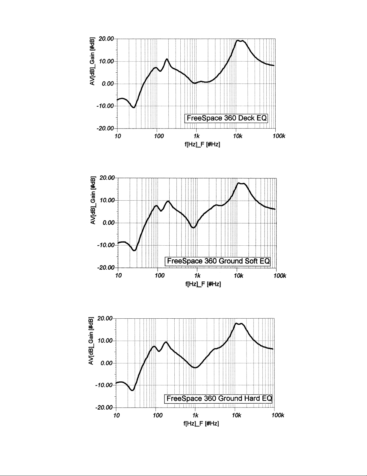
EQUALIZER CARD CURVE DIAGRAMS
Figure 1. FreeSpace® 360 Surface EQ Curve
Figure 2. FreeSpace 360 In-Ground Soft Ground EQ Curve
Figure 3. FreeSpace 360 In-Ground Hard Ground EQ Curve
7
Page 8
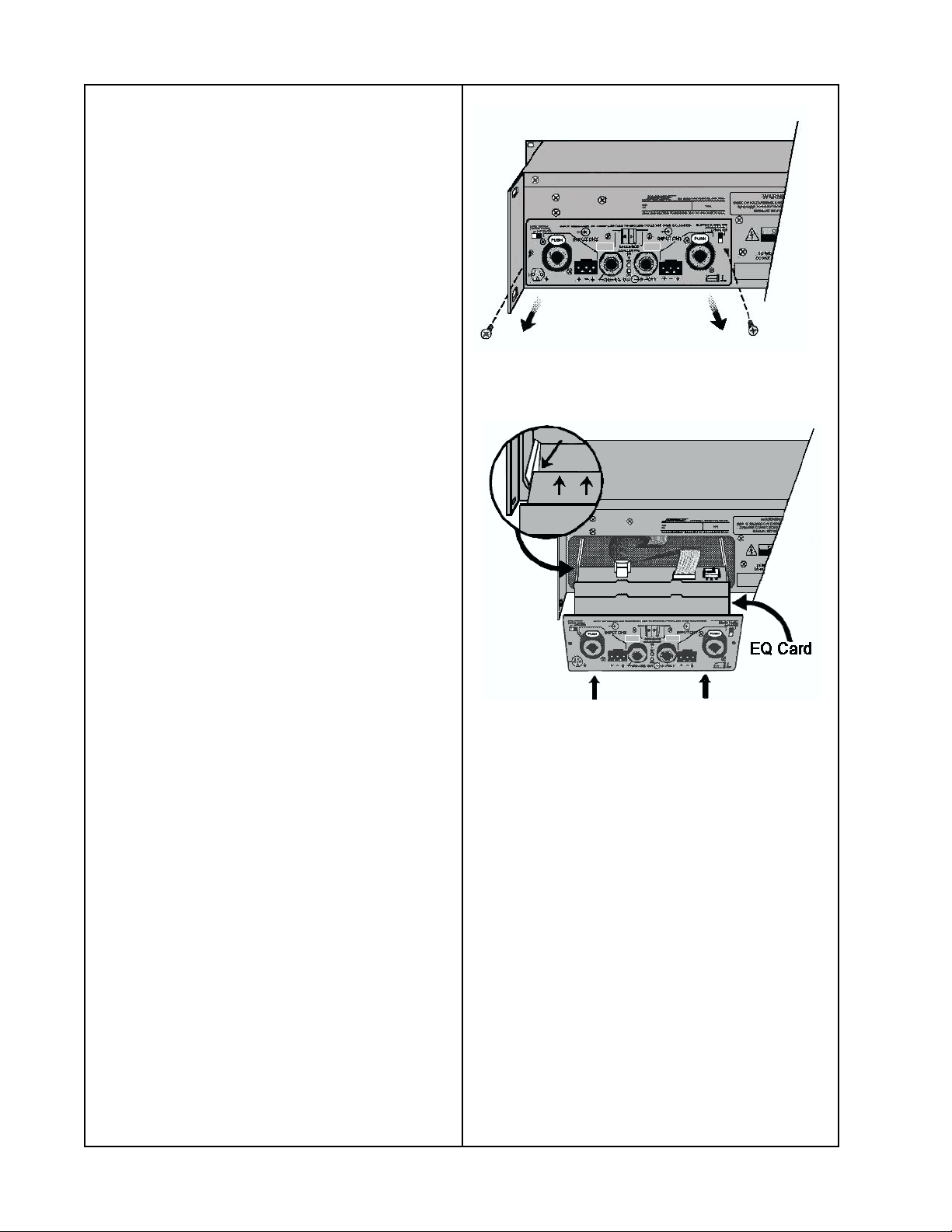
DISASSEMBLY/ASSEMBLY PROCEDURES
1. Input Panel Removal
1.1 Remove the two screws (see figure 4)
holding the panel assembly to the chassis.
1.2 Slide the input panel assembly out of
the chassis to access the EQ cards.
2. Input Panel Replacement
2.1 Slide the input panel assembly back into
the chassis (see figure 5. for proper alignment).
2.2 Secure the input panel to the chassis
using the two screws that had been removed in procedure 1.1.
3. EQ Card Placement
Figure 4. Screw Location
Note: Refer to figure 5. for EQ Card place-
ment.
3.1 Perform procedure 1.
3.2 Place the EQ card into the channel 1 or
2 connector. The connector can be inserted
in only one direction.
3.3 Perform procedure 2.
Figure 5. EQ Card Placement
8
Page 9

TEST SET UP PROCEDURES
1. Install the equalizer card under test into one of the equalizer card jacks located on the input
module of the Bose® 1600 or 1800 series amplifier. Refer to the disassembly/assembly procedures on the previous page.
2. On the amplifier input module, place switch SW1 to the NORM position. Place switch S2 to
the FULL BANDWIDTH position.
3. The input voltage shall be the actual input voltage present at the input, not the open circuit
generator input.
9
Page 10

TEST PROCEDURES
1. Panaray
4402®, 9702®,LT Frequency Response Test
1.1 Apply a 100 mVrms, 700 Hz signal to
the input jack of the amplifier channel under
test.
1.2 Adjust the amplifier volume controls to
maximum and reference a dB meter to the
output. No EQ card installed.
1.3 Shut off the amplifier. Open the input
panel and switch the high frequency/full
range switch (S2) to the full range position.
Insert the EQ card.
1.4 Turn on the amplifier and measure the
response according to the gain chart listed
below.
1.5 Reference a dB meter to the output after
step 1.4 and measure the response of the
EQ card according to the corresponding
chart on this page.
3202 II
4402 II
9702 II
LT II
3202 II EQ Frequency Response
®
Series II EQ PCB 3202®,
EQ Gain Response
+7.0 dB ± 1.0 dB
+5.0 dB ± 1.0 dB
+2.6 dB ± 1.0 dB
+2.7 dB ± 1.0 dB
4402 II EQ Frequency Response
Frequency Output Level
50 Hz -27.4 dB ± 3 dB
150 Hz -2.2 dB ± 1.5 dB
250 Hz 1.7 dB ± 1.5 dB
500 Hz -0.9 dB ± 1.5 dB
700 Hz 0 dB
Reference
1 kHz 1.3 dB ± 1.5 dB
2 kHz -0.3 dB ± 1 dB
3 kHz 0.6 dB ± 1 dB
7 kHz -1.5 dB ± 1.5 dB
13 kHz 0 dB ± 1.5 dB
30 kHz -26 dB ± 3 dB
9702 II EQ Frequency Response
Frequency Output Level
50 Hz -23 dB ± 3 dB
100 Hz -2.4 dB ± 1.5 dB
180 Hz +5.2 dB ± 2 dB
550 Hz -1.5 dB ± 1 dB
700 Hz 0 dB
Reference
1.1 kHz +2.3 dB ± 1 dB
1.8 kHz +3.8 dB ± 1 dB
3 kHz +4.8 dB ± 1 dB
6.5 kHz +4.5 dB ± 1.5 dB
11.5 kHz +3.8 dB ± 1.5 dB
30 kHz -22 dB ± 3 dB
Frequency Output Level
50 Hz -27 dB ± 3 dB
100 Hz -6.0 dB ± 1.5 dB
200 Hz 3.0 dB ± 1.5 dB
400 Hz -1.5 dB ± 1 dB
700 Hz 0 dB
Reference
900 Hz 0.5 dB ± 1 dB
3,250 Hz -6.5 dB ± 1.5 dB
6.4 kHz -6.5 dB ± 1.5 dB
13 kHz -4.3 dB ± 1.5 dB
30 kHz -27 dB ± 3 dB
LT II System EQ Frequency Response
Frequency Output Level
40 Hz -31.7 dB ±3 dB
100 Hz -1.9 dB ±1 dB
190 Hz 7.0 dB ±2dB
300 Hz 2.5 dB ±1 dB
700 Hz 0 dB
Reference
2 kHz -0.4 dB ±1 dB
4 kHz -2.0 dB ±2 dB
10 kHz -30.7 dB ±3 dB
10
Page 11
TEST PROCEDURES
2. 402® EQ PCB Frequency Response Test
2.1 Apply a 100 mVrms, 850 Hz signal to
the input jack of the amplifier channel under
test.
2.2 Adjust the amplifier volume controls to
maximum and reference a dB meter to the
output. No EQ card installed.
2.3 Shut off the amplifier. Open the input panel
and switch the high frequency/full range
switch (S2) to the full range position.
Insert the EQ card.
2.4 Turn on the amplifier and measure the
gain. There should be a - 3.4 dB ± 1.0 dB
change in gain at the output.
2.5 Reference a dB meter and measure
the response of the EQ card according to
the 402 EQ Full Range Response chart.
3. 402 II EQ PCB Frequency Response Test
3.1 Apply a 100 mVrms, 850 Hz signal to
the input jack of the amplifier channel under
test.
3.2 Adjust the amplifier volume controls to
maximum and reference a dB meter to the
output. No EQ card installed.
3.3 Shut off the amplifier. Open the input panel
and switch the high frequency/full range
switch (S2) to the full range position. Insert
the EQ card.
3.4 Turn on the amplifier and measure the gain.
There should be a - 4.2 dB ± 1.0 dB change in
gain at the output.
3.5 Reference a dB meter and measure
the response of the EQ card according to the
402 II EQ Full Range Response chart.
2.6 Shut off the amplifier. Open the input panel
and switch (S2) to the high frequency position.
2.7 Measure the response according to
the 402 EQ High Frequency Response chart.
402 EQ Full Range Frequency Response
Frequency Output Level
60 Hz -3.7 dB ± 1.5 dB
105 Hz +8.5 dB ± 1.5 dB
220 Hz +3.5 dB ± 1.5 dB
850 Hz 0 dB
Reference
4 kHz +5.8 dB ± 1.5 dB
14.5 kHz +13.3 dB ± 1.5 dB
402 EQ High Frequency Response
Frequency Output Level
60 Hz -16.4 dB ± 1.5 dB
105 Hz -5.2 dB ± 1.5 dB
220 Hz +2.8 dB ± 1.5 dB
850 Hz 0 dB
Reference
4 kHz +5.8 dB ± 1.5 dB
14.5 kHz +13.3 dB ± 1.5 dB
3.6 Shut off the amplifier. Open the input panel
and switch (S2) to the high frequency position.
3.7 Measure the response according to the
402 II EQ High Frequency Response chart.
402 II EQ Full Range Frequency Response
Frequency Output Level
60 Hz +3.2 dB ± 1.5 dB
90 Hz +10.0 dB ± 1.5 dB
220 Hz +7.3 dB ± 1.5 dB
600 Hz -2.4 dB ± 1.5 dB
850 Hz 0 dB
Reference
4 kHz +5.6 dB ± 1.5 dB
13.5 kHz +15.5 dB ± 1.5 dB
402 II EQ High Frequency Response
Frequency Output Level
60 Hz -13.0 dB ± 1.5 dB
90 Hz -5.6 dB ± 1.5 dB
220 Hz +6.8 dB ± 1.5 dB
600 Hz -2.4 dB ± 1.5 dB
850 Hz 0 dB
Reference
4 kHz +5.6 dB ± 1.5 dB
13.5 kHz +15.5 dB ± 1.5 dB
11
Page 12
TEST PROCEDURES
®
4. 502
Test
502A EQ Full Range Frequency Response
A EQ PCB Frequency Response
4.1 Apply a 100 mVrms, 600 Hz signal to
the input jack of the amplifier channel under
test.
4.2 Adjust the amplifier volume controls to
maximum and reference a dB meter to the
output. No EQ card installed.
4.3 Shut off the amplifier. Open the input
panel and switch the high frequency/full
range switch (S2) to the full range position.
Insert the EQ card.
4.4 Turn on the amplifier and measure the
gain. There should be a +2.5 dB ± 1.0 dB
change in gain at the output.
4.5 Reference a dB meter and measure
the response of the EQ card according to
the 502A Full Range Response chart.
4.6 Shut off the amplifier. Open the input
panel and switch (S2) to the high frequency
position.
4.7 Measure the response according to
the 502A High Frequency Response chart.
502A EQ High Frequency Response
Frequency Output Level
40 Hz -28.5 dB ± 2.0 dB
140 Hz +2.9 dB ± 1.5 dB
600 Hz 0 dB
Reference
2.2 kHz +3.5 dB ± 1.5 dB
5 kHz +12.5 dB ± 1.5 dB
15 k Hz +19.0 dB ± 1.5 dB
5. 502B EQ PCB Frequency Response Test
5.1 Apply a 100 mVrms, 80 Hz signal to the
input jack of the amplifier channel under test.
5.2 Adjust the amplifier volume controls to
maximum and reference a dB meter to the
output. No EQ card installed.
5.3 Shut off the amplifier. Open the input
panel and switch the high frequency/full
range switch (S2) to the full range position.
Insert the EQ card.
5.4 Turn on the amplifier and measure the
gain. There should be an +8.5 dB ± 1.0 dB
change in gain at the output.
5.5 Reference a dB meter and measure
the response of the EQ card according to
the 502B EQ Response chart.
Frequency Output Level
40 Hz -24.5 dB ± 2.0 dB
140 Hz +4.3 dB ± 1.5 dB
600 Hz 0 dB
Reference
2,2 kHz +3.5 dB ± 1.5 dB
5 kHz +12.5 dB ± 1.5 dB
15 kHz +18.4 dB ± 1.5 dB
502B EQ PCB Frequency Response
Frequency Output Level
40 Hz -5.8 dB ± 2.0 dB
80 Hz 0 dB
Reference
100 Hz +1.3 dB ± 1.0 dB
300 Hz -17.5 dB ± 2.0 dB
12
Page 13

TEST PROCEDURES
®
6. 502
Test
502BEX EQ PCB Frequency Response
BEX EQ PCB Frequency Response
6.1 Apply a 200 mVrms, 100 Hz signal to
the input jack of the amplifier channel under
test.
6.2 Adjust the amplifier volume controls to
maximum and reference a dB meter to the
output. No EQ card installed.
6.3 Shut off the amplifier. Open the input
panel and switch the high frequency/full
range switch (S2) to the full range position.
Insert the EQ card.
6.4 Turn on the amplifier and measure the
gain. There should be an +4.2 dB ± 1.0 dB
change in gain at the output.
6.5 Reference a dB meter and measure
the response of the EQ card according to
the 502B EQ Response chart.
7.4 Place the switch (S1) on the Model 1B
EQ PCB to the FLUSH position. Rotate the
pot R33 fully CW.
7.5 Turn on the amplifier and measure the
gain. There should be an +2.8 dB ± 1.0 dB
change in gain at the output.
7.6 Reference a dB meter and measure
the response of the EQ card according to
the Model 1B Flush EQ Response chart.
Model 1B EQ PCB Flush Frequency
Response
Frequency Output Level
60 Hz +4.25 dB ± 1.5 dB
100 Hz +3.3 dB ± 1.5 dB
200 Hz +0.5 dB ± 1.5 dB
500 Hz +5.25 dB ± 1.5 dB
1 kHz 0 dB
Reference
2 kHz -1.0 dB ± 1.5 dB
8 kHz +7.75 dB ± 1.5 dB
10 kHz +9.5 dB ± 2.5 dB
Frequency Output Level
30 Hz -15.2 dB ± 2.0 dB
55 Hz +2.3 dB ± 1.4 dB
100 Hz 0 dB
Reference
160 Hz - 6.8 dB ± 1.0 dB
240 Hz -0.8 dB ± 1.2 dB
500 Hz -11.6 dB ± 2.0 dB
7. Model 1B EQ PCB Flush Frequency
Response Test
7.1 Apply a 200 mVrms, 100 Hz signal to
the input jack of the amplifier channel under
test.
7.2 Adjust the amplifier volume controls to
maximum and reference a dB meter to the
output. No EQ card installed.
7.3 Shut off the amplifier. Open the input
panel and switch the high frequency/full
range switch (S2) to the full range position.
Insert the EQ card.
7.7 Shut off the amplifier and place the
switch (S1) on the Model 1B EQ PCB to the
SURFACE position.
7.8 Replace the input card into the amplifier
and turn the amplifier on.
7.9 Reference a dB meter and measure
the response of the EQ card according to
the Model 1B EQ Surface Frequency
Response chart.
Model 1B EQ Surface Frequency
Response
Frequency Output Level
200 Hz +0.5 dB ± 1.5 dB
500 Hz +0.6 dB ± 1.5 dB
1 kHz 0 dB
Reference
2 kHz -1.3 dB ± 1.5 dB
8 kHz +7.6 dB ± 1.5 dB
10 kHz +7.8 dB ± 2.5 dB
13
Page 14
TEST PROCEDURES
8. 802
®
EQ PCB Frequency Response Test
8.1 Apply a 100 mVrms, 700 Hz signal to the
input jack of the amplifier channel under test.
8.2 Adjust the amplifier volume controls to
maximum and reference a dB meter to the
output. No EQ card installed.
8.3 Shut off the amplifier. Open the input panel
and switch the high frequency/full range
switch (S2) to the full range position. Insert
the EQ card.
8.4 Turn on the amplifier and measure the
gain. There should be a +1. 7 dB ± 1.0 dB
change in gain at the output.
8.5 Reference a dB meter and measure the
response of the EQ card according to the 802
Full Range Response chart on this page.
8.6 Shut off the amplifier. Open the input panel
and switch the high frequency/full range
switch (S2) to the high frequency position.
8.7 Measure the response according to the
802 EQ High Frequency Response.
802 EQ PCB Full Range Frequency
Response
Frequency Output Level
40 Hz +8.0 dB ± 1.5 dB
55 Hz +13.5 dB ± 1.5 dB
140 Hz +6.6 dB ± 1.5 dB
700 Hz 0 dB
Reference
2.5 kHz +2.1 dB ± 1.5 dB
6 kHz +9.6 dB ± 1.5 dB
14.5 kHz +16.7 dB ± 1.5 dB
802 EQ PCB High Frequency Response
Frequency Output Level
40 Hz -21.0 dB ± 1.5 dB
60 Hz -11.5 dB ± 1.5 dB
700 Hz 0 dB
Reference
2.5 kHz +2.1 dB ± 1.5 dB
6 kHz +9.6 dB ± 1.5 dB
14.5 kHz +16.7 dB ± 1.5 dB
9. 802 III EQ PCB Frequency Response Test
9.1 Apply a 100 mVrms, 700 Hz signal to the
input jack of the amplifier channel under
test.
9.2 Adjust the amplifier volume controls to
maximum and reference a dB meter to the
output. No EQ card installed.
9.3 Shut off the amplifier. Open the input panel
and switch the high frequency/full range
switch (S2) to the full range position. Insert
the EQ card.
9.4 Turn on the amplifier and measure the gain.
There should be a +1. 7 dB ± 1.0 dB change
in gain at the output.
9.5 Reference a dB meter and measure
the response of the EQ card according to the
802 III Full Range Response chart.
9.6 Shut off the amplifier. Open the input panel
and switch the high frequency/full range
switch (S2) to the high frequency position.
9.7 Measure the response according to
the 802 III EQ High Frequency Response.
802 III EQ PCB Full Range Frequency
Response
Frequency Output Level
40 Hz +1.9 dB ± 1.5 dB
70 Hz +13.5 dB ± 1.5 dB
140 Hz +7.5 dB ± 1.5 dB
700 Hz 0 dB
Reference
2.5 kHz +1.8 dB ± 1.5 dB
6 kHz +6.9 dB ± 1.5 dB
13 kHz +13.8 dB ± 1.5 dB
802 III EQ PCB High Frequency Response
Frequency Output Level
40 Hz -24.9 dB ± 1.5 dB
70 Hz -10.6 dB ± 1.5 dB
140 Hz +5.2 dB ± 1.5 dB
700 Hz 0 dB
Reference
2.5 kHz +1.9 dB ± 1.5 dB
6 kHz +7.0 dB ± 1.5 dB
13 kHz +13.9 dB ± 1.5 dB
14
Page 15
TEST PROCEDURES
10. Model 8 EQ PCB Frequency Response
Test
10.1 Apply a 100 mVrms, 1 kHz signal to
the input jack of the amplifier channel under
test.
10.2 Adjust the amplifier volume controls to
maximum and reference a dB meter to the
output. No EQ card installed.
10.3 Shut off the amplifier. Open the input
panel and switch the high frequency/full
range switch (S2) to the full range position.
Insert the EQ card.
10.4 Turn on the amplifier and measure the
gain. There should be a -3.5 dB ± 1.0 dB
change in gain at the output.
10.5 Reference a dB meter and measure
the response of the EQ card according to
the Model 8 Full Range Response chart
below.
11. Model 25/32 EQ PCB Frequency
Response Test
11.1 Apply a 100 mVrms, 1 kHz signal to
the input jack of the amplifier channel under
test.
11.2 Adjust the amplifier volume controls to
maximum and reference a dB meter to the
output. No EQ card installed..
11.3 Shut off the amplifier. Open the input
panel and switch the high frequency/full
range switch (S2) to the full range position.
Insert the EQ card.
11.4 Turn on the amplifier and measure the
gain. There should be a -4.8 dB ± 1.0 dB
change in gain at the output.
11.5 Reference a dB meter and measure
the response of the EQ card according to
the Model 25/32 Full Range Response.
Model 8 Frequency Response
Frequency Output Level
95 Hz +11.3 dB ± 1.5 dB
250 Hz +4.5 dB ± 1.5 dB
1 kHz 0 dB
Reference
2 kHz +3.0 dB ± 1.5 dB
4 kHz +7.0 dB ± 1.5 dB
8 kHz +10.5 dB ± 1.5 dB
12.5 kHz +11.75 dB ± 2.5 dB
Model 25/32 Frequency Response
Frequency Output Level
95 Hz +12.3 dB ± 1.5 dB
250 Hz +4.4 dB ± 1.5 dB
1 kHz 0 dB
Reference
2 kHz +1.7 dB ± 1.5 dB
4 kHz +7.6 dB ± 1.5 dB
8 kHz +12.0 dB ± 1.5 dB
12.5 kHz +15.0 dB ± 2.5 dB
15
Page 16
TEST PROCEDURES
12. FreeSpace® 360 In Soft Ground
Frequency Response Test
12.1 Apply a 100 mVrms, 1 kHz signal to
the input jack of the amplifier channel under
test.
12.2 Adjust the amplifier volume controls to
maximum and reference a dB meter to the
output. No EQ card installed.
12.3 Shut off the amplifier. Open the input
panel and switch the high frequency/full
range switch (S2) to the full range position.
Switch the switch on the EQ card to the
SOFT position and insert the EQ card.
12.4 Turn on the amplifier and measure the
gain. There should be a 0.0 ± 1.0 dB
change in gain at the output.
12.5 Reference a dB meter and measure
the response of the EQ card according to
the In Soft Ground Frequency Response
chart.
In Soft Ground Frequency Response
Frequency Output Level
30 Hz -10.3 dB ± 1.5 dB
180 Hz +9.5 dB ± 1.5 dB
190 Hz +7.8 dB ± 1.5 dB
1 kHz 0 dB
Reference
3 kHz +8.1 dB ± 1.0 dB
4 kHz +7.8 dB ± 1.0 dB
10 kHz +16.4 dB ± 2.5 dB
13.3 Shut off the amplifier. Open the input
panel and switch the high frequency/full
range switch (S2) to the full range position.
NOTE: Switch the switch (S1) on the EQ
card to the HARD position and insert the
EQ card.
13.4 Turn on the amplifier and measure the
gain. There should be a -2.1 ± 1.0 dB
change in gain at the output.
13.5 Reference a dB meter and measure
the response according to the In Hard
Ground Frequency Response chart.
In Hard Ground Frequency Response
Frequency Output Level
30 Hz -8.3 dB ± 1.5 dB
90 Hz +9.8 dB ± 1.5 dB
180 Hz +11.2 dB ± 1.0 dB
800 Hz +0.8 dB ± 1.0 dB
1 kHz 0 dB
Reference
3 kHz +8.1 dB ± 1.0 dB
4 kHz +8.7 dB ± 1.0 dB
10 kHz +18.2 dB ± 2.5 dB
13. FreeSpace 360 In Hard Ground
Frequency Response Test.
13.1 Apply a 100 mVrms, 1 kHz signal to
the input jack of the amplifier channel under
test.
13.2 Adjust the amplifier volume controls to
maximum and reference a dB meter to the
output. No EQ card installed.
16
Page 17
TEST PROCEDURES
14. FreeSpace® 360 Surface EQ PCB
Frequency Response Test.
14.1 Apply a 100 mVrms, 1 kHz signal to
the input jack of the amplifier channel under
test.
14.2 Adjust the amplifier volume controls to
maximum and reference a dB meter to the
output. No EQ card installed.
14.3 Shut off the amplifier. Open the input
panel and switch the high frequency/full
range switch (S2) to the full range position.
NOTE: Switch the switch (S1) on the EQ
card to the SOFT position and insert the
EQ card.
14.4 Turn on the amplifier and measure the
gain. There should be a +1.0 ± 1.0 dB
change in gain at the output.
14.5 Reference a dB meter and measure
the response of the EQ card according to
the Surface Frequency Response chart.
15. Distortion Test
15.1 Apply a signal from the chart below to
the input jack of the amplifier channel under
test.
15.2 Measure the distortion level at the
output of the amplifier. It should be £ 0.1%
THD.
Product Input Level Frequency
402
402
II
802
II
802
III
502A
502B 700 mVrms 80 Hz
502BEX 4.5 Vrms 100 Hz
M 1B 750 mVrms 1 kHz
M 8 750 mVrms 1 kHz
M 25/32 750 mVrms 1 kHz
3202
4402
9702
1.4 Vrms 850 Hz
1.4 Vrms 850 Hz
750 mVrms 700 Hz
750 mVrms 700 Hz
730 mVrms 600 Hz
II
II
II
4 Vrms 320 Hz
4 Vrms 320 Hz
4 Vrms 320 Hz
360 Surface Frequency Response
Frequency Output Level
30 Hz -8.8 dB ± 1.5 dB
90 Hz +7.2 dB ± 1.5 dB
180 Hz +11.0 dB ± 1.5 dB
900 Hz +0.2 dB ± 1.5 dB
1 kHz 0 dB
Reference
2 kHz +0.4 dB ± 1.5 dB
5 kHz +6.7 dB ± 1.0 dB
10 kHz +17.9 dB ± 2.5 dB
17
Page 18

PART LIST NOTES
1. This part is not normally available from Customer Service. Approval from the Field Service
Manager is required before ordering.
2. The individual parts located on the PCBs are listed in the Electrical Part List.
3. This part is critical for safety purposes. Failure to use a substitute replacement with the
same safety characteristics as the recommended replacement part might create shock, fire
and/or other hazards.
4. This connector is used on the 502®B EQ PCB only.
EQ CARD PCB
PART NUMBERS AND PRODUCT CODES
PCB Part Number Description Product Code
177333
258111
177356
258115
177342 502A EQ Card 009082
177349 502B EQ Card 009081
191921 502BEX EQ Card 019551
183111-001
183123-001
183105-001
183117-001
190670-001E Model 1B EQ Card 019509
184825 Model 8 EQ Card 015134
183744 Model 32 EQ Card 011687
198379-0011E
198383-0011E FreeSpace 360 In-ground 021844
Panaray
Panaray 4402 II EQ Card
Panaray 9702 II EQ Card
402 EQ Card
402 II EQ Card
II EQ Card
802
802 III EQ Card
3302 II EQ Card
Panaray LT II EQ Card
FreeSpace
360 Surface
009083
026677
009080
026679
011502
011504
017929
018485
021845
18
Page 19
402® SERIES I ELECTRICAL PART LIST
Resistors
Reference
Designator
R1 10.0K, 1206, 1/8W, 1% 124894-1002
R2 10.0K, 1206, 1/8W, 1% 124894-1002
R3 3.92K, 1206, 1/8W, 1% 124894-3921
R4 3.92K, 1206, 1/8W, 1% 124894-3921
R5 8.25K, 1206, 1/8W, 1% 124894-8251
R6 1.82K, 1206, 1/8W, 1% 124894-1821
R7 1.82K, 1206, 1/8W, 1% 124894-1821
R11 100K, 1206, 1/8W, 1% 124894-1003
R13 JUMPER, CHIP 124896
R14 3.92K, 1206, 1/8W, 1% 124894-3921
R17 5.11K, 1206, 1/8W, 1% 124894-5111
R19 JUMPER, CHIP 124896
R20 JUMPER, CHIP 124896
R21 JUMPER, CHIP 124896
R27 JUMPER, CHIP 124896
R30 86.6K, 1206, 1/8W, 1% 124894-8662
R31 21.5K, 1206, 1/8W, 1% 124894-2152
R32 78.7K, 1206, 1/8W, 1% 124894-7872
R33 6.49K, 1206, 1/8W, 1% 124894-6491
R34 JUMPER, CHIP 124896
R35 JUMPER, CHIP 124896
R36 JUMPER, CHIP 124896
R37 47.0K, 1206, 1/8W, 5% 124895-4735
R38 47.0K, 1206, 1/8W, 5% 124895-4735
R39 JUMPER, CHIP 124896
Description Part
Number
Note
Capacitors
Reference
Designator
C2 .1uF, BOX, 85, 50V, 5% 137127-104
C3 27uF, BOX, 85, 50V, 5% 137127-274
C4 .0047uF, BOX, 85, 100V, 5% 137127-472
C5 680pF, CER, 10%, 50V 137269-681
C6 .0022uF, BOX, 85, 100V, 5% 137127-222
C7 .047uF, BOX, 85, 63V, 5% 137127-473
C8 .047uF, BOX, 85, 63V, 5% 137127-473
C17 .068uF, BOX, 85, 63V, 5% 137127-683
C19 .068uF, BOX, 85, 63V, 5% 137127-683
C20 .022uF, BOX, 85, 100V, 5% 137127-223
C22 .022uF, BOX, 85, 100V, 5% 137127-223
C24 10000pF, CHIP, 5% 124959-103
C26 10000pF, CHIP, 5% 124959-103
C48 10000pF, CHIP, 5% 124959-103
C49 10000pF, CHIP, 5% 124959-103
C50 10000pF, CHIP, 5% 124959-103
C51 10000pF, CHIP, 5% 124959-103
Description Part
Number
Note
19
Page 20
402® SERIES I ELECTRICAL PART LIST
Diodes
Reference
Designator
D1 1N4148, 52MM AXIAL 121501
D2 1N4148, 52MM AXIAL 121501
D3 1N4148, 52MM AXIAL 121501
D4 1N4746, ZEN, 18V, 1W, 5% 116995-4746A
D5 1N4148, 52MM AXIAL 121501
D6 1N4746, ZEN, 18V, 1W, 5% 116995-4746A
Reference
Designator
U1 NJM2059, OP AMP, QUAD 144008
U2 NJM2059, OP AMP, QUAD 144008
U3 BA3128N, SWITCH, ACTIVE, SIP-8 177292
Reference
Designator
J1 CONN, HEADER, 12 PIN 149538
Description Part
Number
Integrated circuits
Description Part
Number
Connectors
Description Part
Number
Note
Note
Note
20
Page 21

402® SERIES II ELECTRICAL PART LIST
Resistors
Reference
Designator
R1 10.0K, 1206, 1/8W, 1% 124894-1001
R2 1.00K, 1206, 1/8W, 1% 124894-1001
R3 2.21K, 1206, 1/8W, 1% 124894-2211
R4 1.47K, 1206, 1/8W, 1% 124894-1471
R5 JUMPER, CHIP 124896
R8 182K, 1206, 1/8W, 1% 124894-1823
R9 3.83K, 1206, 1/8W, 1% 124894-3831
R10 25.5K, 1206, 1/8W, 1% 124894-2552
R12 5.76K, 1206, 1/8W, 1% 124894-5761
R13 1.00K, 1206, 1/8W, 1% 124894-1001
R14 2.00K, 1206, 1/8W, 1% 124894-2001
R17 10.0K, 1206, 1/8W, 1% 124894-1002
R19 JUMPER, CHIP 124896
R20 JUMPER, CHIP 124896
R21 30.1K, 1206, 1/8W, 1% 124894-3012
R22 JUMPER, CHIP 124896
R23 5.76K, 1206, 1/8W, 1% 124894-5761
R24 2.00K, 1206, 1/8W, 1% 124894-2001
R26 3.01K, 1206, 1/8W, 1% 124894-3011
R27 634 OHM, 1206, 1/8W, 1% 124894-6340
R30 75.0K, 1206, 1/8W, 1% 124894-7502
R31 21.5K, 1206, 1/8W, 1% 124894-2152
R32 78.7K, 1206, 1/8W, 1% 124894-7872
R33 7.15K, 1206, 1/8W, 1% 124894-7151
R35 JUMPER, CHIP 124896
R36 JUMPER, CHIP 124896
R37 47.5K, 1206, 1/8W, 1% 124894-4752
R38 47.5K, 1206, 1/8W, 1% 124894-4752
R39 JUMPER, CHIP 124896
Description Part
Number
Note
21
Page 22
402® SERIES II ELECTRICAL PART LIST
Capacitors
Reference
Designator
C3 .0022uF, BOX, 85, 100V, 5% 137127-222
C5 .0018uF, BOX, 85, 100V, 5% 137127-182
C8 .082uF, BOX, 85, 50V, 5% 137127-823
C10 .01uF, BOX, 85, 100V, 5% 137127-103
C14 .022uF, BOX, 85, 100V, 5% 137127-223
C15 .068uF, BOX, 85, 63V, 5% 137127-683
C16 .047uF, BOX, 85, 63V, 5% 137127-473
C17 .082uF, BOX, 85, 50V, 5% 137127-823
C19 .082uF, BOX, 85, 50V, 5% 137127-823
C20 .022uF, BOX, 85, 100V, 5% 137127-223
C22 .022uF, BOX, 85, 100V, 5% 137127-223
C23 .027uF, BOX, 85, 63V, 5% 137127-273
C24 10000pF, CHIP, 5% 124959-103
C26 10000pF, CHIP, 5% 124959-103
C48 10000pF, CHIP, 5% 124959-103
C49 10000pF, CHIP, 5% 124959-103
C50 10000pF, CHIP, 5% 124959-103
C51 10000pF, CHIP, 5% 124959-103
Description Part
Number
Diodes
Note
Reference
Designator
D1 1N4148, 52MM AXIAL 121501
D2 1N4148, 52MM AXIAL 121501
D3 1N4148, 52MM AXIAL 121501
D4 1N4746, ZEN, 18V, 1W, 5% 116995-4746A
D5 1N4148, 52MM AXIAL 121501
D6 1N4746, ZEN, 18V, 1W, 5% 116995-4746A
Reference
Designator
U1 NJM2059, OP AMP, QUAD 144008
U2 NJM2059, OP AMP, QUAD 144008
U3 BA3128N, SWITCH, ACTIVE, SIP-8 177292
Reference
Designator
J1 CONN, HEADER, 12 PIN 149538
Description Part
Number
Integrated Circuits
Description Part
Number
Connectors
Description Part
Number
Note
Note
Note
22
Page 23

802® SERIES II ELECTRICAL PART LIST
Resistors
Reference
Designator
R1 3.32K, 1206, 1/8W, 1% 124894-3321
R2 1.00K, 1206, 1/8W, 1% 124894-1001
R3 1.27K, 1206, 1/8W, 1% 124894-1271
R4 1.27K, 1206, 1/8W, 1% 124894-1271
R5 JUMPER, CHIP 124896
R8 9.09K, 1206, 1/8W, 1% 124894-9091
R9 6.81K, 1206, 1/8W, 1% 124894-6811
R10 3.01K, 1206, 1/8W, 1% 124894-3011
R12 9.09K, 1206, 1/8W, 1% 124894-9091
R13 5.62K, 1206, 1/8W, 1% 124894-5621
R14 54.9K, 1206, 1/8W, 1% 124894-5492
R15 61.9K, 1206, 1/8W, 1% 124894-6192
R16 2.49K, 1206, 1/8W, 1% 124894-2491
R19 JUMPER, CHIP 124896
R20 JUMPER, CHIP 124896
R22 JUMPER, CHIP 124896
R26 16.5K, 1206, 1/8W, 1% 124894-1652
R27 20.0K, 1206, 1/8W, 1% 124894-2002
R29 1.74K, 1206, 1/8W, 1% 124894-1741
R30 93.1K, 1206, 1/8W, 1% 124894-9312
R31 2.00K, 1206, 1/8W, 1% 124894-2001
R32 34.8K, 1206, 1/8W, 1% 124894-3482
R33 6.34K, 1206, 1/8W, 1% 124894-6341
R37 47.5K, 1206, 1/8W, 1% 124894-4752
R38 47.5K, 1206, 1/8W, 1% 124894-4752
R39 JUMPER, CHIP 124896
R40 JUMPER, CHIP 124896
R41 JUMPER, CHIP 124896
R44 JUMPER, CHIP 124896
Description Part
Number
Note
23
Page 24
802® SERIES II ELECTRICAL PART LIST
Capacitors
Reference
Designator
C3 .0068uF, BOX, 85, 100V, 5% 137127-682
C5 .0027uF, BOX, 85, 100V, 5% 137127-272
C8 .12uF, BOX, 85, 50V, 5% 137127-124
C10 .033uF, BOX, 85, 63V, 5% 137127-333
C11 .0082uF, BOX, 85, 100V, 5% 137127-822
C12 .0056uF, BOX, 85, 100V, 5% 137127-562
C16 .1uF, BOX, 85, 50V, 5% 137127-104
C18 .1uF, BOX, 85, 50V, 5% 137127-104
C19 .1uF, BOX, 85, 50V, 5% 137127-104
C20 .47uF, BOX, 85, 50V, 5% 137127-474
C21 .15uF, BOX, 85, 50V, 5% 137127-154
C22 .15uF, BOX, 85, 50V, 5% 137127-154
C23 .033uF, BOX, 85, 63V, 5% 137127-333
C24 10000pF, CHIP, 5% 124959-103
C26 10000pF, CHIP, 5% 124959-103
C48 10000pF, CHIP, 5% 124959-103
C49 10000pF, CHIP, 5% 124959-103
C50 10000pF, CHIP, 5% 124959-103
C51 10000pF, CHIP, 5% 124959-103
Description Part
Number
Note
Diodes
Reference
Designator
D1 1N4148, 52MM AXIAL 121501
D2 1N4148, 52MM AXIAL 121501
D3 1N4148, 52MM AXIAL 121501
D4 1N4746, ZEN, 18V, 1W, 5% 116995-4746A
D5 1N4148, 52MM AXIAL 121501
D6 1N4746, ZEN, 18V, 1W, 5% 116995-4746A
Reference
Designator
U1 NJM2059OP, AMP, QUAD 144008
U2 NJM2059OP, AMP, QUAD 144008
U3 BA3128N, SWITCH, ACTIVE, SIP-8 177292
Reference
Designator
J1 CONN, HEADER, 12 PIN 149538
Description Part
Number
Integrated Circuits
Description Part
Number
Connectors
Description Part
Number
Note
Note
Note
24
Page 25

802® SERIES III ELECTRICAL PART LIST
Resistors
Reference
Designator
R1 3.32K, 1206, 1/8W, 1% 124894-3321
R2 1.00K, 1206, 1/8W, 1% 124894-1001
R3 1.27K, 1206, 1/8W, 1% 124894-1271
R4 1.27K, 1206, 1/8W, 1% 124894-1271
R5 JUMPER, CHIP 124896
R8 9.09K, 1206, 1/8W, 1% 124894-9091
R9 6.81K, 1206, 1/8W, 1% 124894-6811
R10 3.01K, 1206, 1/8W, 1% 124894-3311
R12 9.09K, 1206, 1/8W, 1% 124894-9091
R13 5.62K, 1206, 1/8W, 1% 124894-5621
R14 54.9K, 1206, 1/8W, 1% 124894-5492
R15 61.9K, 1206, 1/8W, 1% 124894-6192
R16 2.49K, 1206, 1/8W, 1% 124894-2491
R19 JUMPER, CHIP 124896
R20 JUMPER, CHIP 124896
R22 JUMPER, CHIP 124896
R26 16.5K, 1206, 1/8W, 1% 124894-1652
R27 20.0K, 1206, 1/8W, 1% 124894-2002
R29 1.74K, 1206, 1/8W, 1% 124894-1741
R30 93.1K, 1206, 1/8W, 1% 124894-9312
R31 2.00K, 1206, 1/8W, 1% 124894-2001
R32 34.8K, 1206, 1/8W, 1% 124894-3482
R33 6.34K, 1206, 1/8W, 1% 124894-6341
R37 47.5K, 1206, 1/8W, 1% 124894-4752
R38 47.5K, 1206, 1/8W, 1% 124894-4752
R39 JUMPER, CHIP 124896
R40 JUMPER, CHIP 124896
R41 JUMPER, CHIP 124896
R44 JUMPER, CHIP 124896
Description Part
Number
Note
25
Page 26

802® SERIES III ELECTRICAL PART LIST
Capacitors
Reference
Designator
C3 .0068uF, BOX, 85, 100V, 5% 137127-682
C5 .0027uF, BOX, 85, 100V, 5% 137127-272
C8 .12uF, BOX, 85, 50V, 5% 137127-124
C10 .033uF, BOX, 85, 63V, 5% 137127-333
C11 .0082uF, BOX, 85, 100V, 5% 137127-822
C12 .0056uF, BOX, 85, 100V, 5% 137127-562
C16 .1uF, BOX, 85, 50V, 5% 137127-104
C18 .1uF, BOX, 85, 50V, 5% 137127-104
C19 .1uF, BOX, 85, 50V, 5% 137127-104
C20 .47uF, BOX, 85, 50V, 5% 137127-474
C21 .15uF, BOX, 85, 50V, 5% 137127-154
C22 .15uF, BOX, 85, 50V, 5% 137127-154
C23 .033uF, BOX, 85, 63V, 5% 137127-333
C24 10000pF, CHIP, 5% 124959-103
C26 10000pF, CHIP, 5% 124959-103
C48 10000pF, CHIP, 5% 124959-103
C49 10000pF, CHIP, 5% 124959-103
C50 10000pF, CHIP, 5% 124959-103
C51 10000pF, CHIP, 5% 124959-103
Description Part
Number
Note
Diodes
Reference
Designator
D1 1N4148, 52MM AXIAL 121501
D2 1N4148, 52MM AXIAL 121501
D3 1N4148, 52MM AXIAL 121501
D4 1N4746, ZEN, 18V, 1W, 5% 116995-4746A
D5 1N4148, 52MM AXIAL 121501
D6 1N4746, ZEN, 18V, 1W, 5% 116995-4746A
Reference
Designator
U1 NJM2059, OP AMP, QUAD 144008
U2 NJM2059, OP AMP, QUAD 144008
U3 BA3128N, SWITCH, ACTIVE, SIP-8 177292
Reference
Designator
J1 CONN, HEADER, 12 PIN 149538
Description Part
Number
Integrated Circuits
Description Part
Number
Connectors
Description Part
Number
Note
Note
Note
26
Page 27

502®A ELECTRICAL PART LIST
Resistors
Reference
Designator
R1 3.65K, 1206, 1/8W, 1% 124894-3651
R2 2.00K, 1206, 1/8W, 1% 124894-2001
R3 4.02K, 1206, 1/8W, 1% 124894-4021
R4 4.02K, 1206, 1/8W, 1% 124894-4021
R5 JUMPER, CHIP 124896
R8 30.1K, 1206, 1/8W, 1% 124894-3012
R11 49.9K, 1206, 1/8W, 1% 124894-4992
R12 2.32K, 1206, 1/8W, 1% 124894-2321
R13 2.00K, 1206, 1/8W, 1% 124894-2001
R14 13.0K, 1206, 1/8W, 1% 124894-1302
R15 20.0K, 1206, 1/8W, 1% 124894-2002
R16 1.33K, 1206, 1/8W, 1% 124894-1331
R17 100K, 1206, 1/8W, 1% 124894-1003
R18 3.16K, 1206, 1/8W, 1% 124894-3161
R19 511 OHM, 1206, 1/8W, 1% 124894-5110
R20 JUMPER, CHIP 124896
R21 18.2K, 1206, 1/8W, 1% 124894-1822
R22 274 OHM, 1206, 1/8W, 1% 124894-2740
R23 8.66K, 1206, 1/8W, 1% 124894-8661
R24 6.34K, 1206, 1/8W, 1% 124894-6341
R25 274 OHM, 1206, 1/8W, 1% 124894-2740
R26 1.91K, 1206, 1/8W, 1% 124894-1911
R27 2.21K, 1206, 1/8W, 1% 124894-2211
R28 2.43K, 1206, 1/8W, 1% 124894-2431
R29 2.00K, 1206, 1/8W, 1% 124894-2001
R30 43.2K, 1206, 1/8W, 1% 124894-4322
R31 3.01K, 1206, 1/8W, 1% 124894-3011
R32 41.2K, 1206, 1/8W, 1% 124894-4122
R33 3.92K, 1206, 1/8W, 1% 124894-3921
R37 47.0K, 1206, 1/8W, 5% 124895-4735
R38 47.0K, 1206, 1/8W, 5% 124895-4735
R39 JUMPER, CHIP 124896
Description Part
Number
Note
27
Page 28

502®A ELECTRICAL PART LIST
Capacitors
Reference
Designator
C2 100pF, CER, 10%, 50V 137269-101
C3 .01uF, BOX, 85, 100V, 5% 137127-103
C5 680pF, CER, 10%, 50V 137269-681
C8 .0047uF, BOX, 85, 100V, 5% 137127-472
C10 .0047uF, BOX, 85, 100V, 5% 137127-472
C11 .01uF, BOX, 85, 100V, 5% 137127-103
C12 .01uF, BOX, 85, 100V, 5% 137127-103
C14 .1uF, BOX, 85, 50V, 5% 137127-104
C15 .1uF, BOX, 85, 50V, 5% 137127-104
C16 100pF, CER, 10%, 50V 137269-101
C17 .47uF, BOX, 85, 50V, 5% 137127-474
C18 .1uF, BOX, 85, 50V, 5% 137127-104
C19 .1uF, BOX, 85, 50V, 5% 137127-104
C20 .47uF, BOX, 85, 50V, 5% 137127-474
C21 .1uF, BOX, 85, 50V, 5% 137127-104
C22 .1uF, BOX, 85, 50V, 5% 137127-104
C23 .01uF, BOX, 85, 100V, 5% 137127-103
C24 10000pF, CHIP, 5% 124959-103
C25 .047uF, BOX, 85, 63V, 5% 137127-473
C26 10000pF, CHIP, 5% 124959-103
C48 10000pF, CHIP, 5% 124959-103
C49 10000pF, CHIP, 5% 124959-103
C50 10000pF, CHIP, 5% 124959-103
C51 10000pF, CHIP, 5% 124959-103
Description Part
Number
Note
Diodes
Reference
Designator
D1 1N4148, 52MM AXIAL 121501
D2 1N4148, 52MM AXIAL 121501
D3 1N4148, 52MM AXIAL 121501
D4 1N4746, ZEN, 18V, 1W, 5% 116995-4746A
D5 1N4148, 52MM AXIAL 121501
D6 1N4746, ZEN, 18V, 1W, 5% 116995-4746A
Reference
Designator
U1 NJM2059, OP AMP, QUAD 144008
U2 NJM2059, OP AMP, QUAD 144008
U3 BA3128N, SWITCH, ACTIVE, SIP-8 177292
Reference
Designator
J1 CONN,HEADER, 12 PIN 149538
Description Part
Number
Integrated Circuits
Description Part
Number
Connectors
Description Part
Number
Note
Note
Note
28
Page 29

502®B ELECTRICAL PART LIST
Resistors
Reference
Designator
R35 6.81K, 1206, 1/8W, 1% 124894-6811
R36 4.75K, 1206, 1/8W, 1% 124894-4751
R37 15.4K, 1206, 1/8W, 1% 124894-1542
R38 4.75K, 1206, 1/8W, 1% 124894-4751
R39 JUMPER, CHIP 124896
R40 5.11K, 1206, 1/8W, 1% 124894-5111
R41 221K, 1206, 1/8W, 1% 124894-2213
R42 1.10K, 1206, 1/8W, 1% 124894-1101
R43 49.9K, 1206, 1/8W, 1% 124894-4992
R44 221K, 1206, 1/8W, 1% 124894-2213
R45 68.1K, 1206, 1/8W, 1% 124894-6812
R46 6.98K, 1206, 1/8W, 1% 124894-6981
R47 1.00K, 1206, 1/8W, 1% 124894-1001
R48 4.32K, 1206, 1/8W, 1% 124894-4321
R49 5.49K, 1206, 1/8W, 1% 124894-5491
R50 14.0K, 1206, 1/8W, 1% 124894-1402
R51 14.0K, 1206, 1/8W, 1% 124894-1402
R52 6.81K, 1206, 1/8W, 1% 124894-6811
Description Part
Number
Capacitors
Note
Reference
Designator
C26 100pF, CER, 10%, 50V 137269-101
C27 100pF, CER, 10%, 50V 137269-101
C28 .47uF, BOX, 85, 50V, 5% 137127-474
C29 .22uF, BOX, 85, 50V, 5% 137127-224
C30 .22uF, BOX, 85, 50V, 5% 137127-224
C31 .1uF, BOX, 85, 50V, 5% 137127-104
C32 .1uF, BOX, 85, 50V, 5% 137127-104
C34 .22uF, BOX, 85, 50V, 5% 137127-224
C35 .022uF, BOX, 85, 100V, 5% 137127-223
C36 .18uF, BOX, 85, 50V, 5% 137127-184
C52 10000pF, CHIP ,5% 124959-103
C53 10000pF, CHIP ,5% 124959-103
C54 10000pF, CHIP ,5% 124959-103
C55 10000pF, CHIP ,5% 124959-103
Description Part
Number
Note
29
Page 30

502®B ELECTRICAL PART LIST
Diodes
Reference
Designator
D1 1N4148, 52MM AXIAL 121501
D2 1N4148, 52MM AXIAL 121501
D3 1N4148, 52MM AXIAL 121501
D4 1N4746, ZEN, 18V, 1W, 5% 116995-4746A
D5 1N4148, 52MM AXIAL 121501
D6 1N4746, ZEN, 18V, 1W, 5% 116995-4746A
D7 1N4148, 52MM AXIAL 121501
D8 1N4148, 52MM AXIAL 121501
Reference
Designator
U1 NJM2059, OP AMP, QUAD 144008
U2 NJM2059, OP AMP, QUAD 144008
Reference
Designator
J1 CONN, HEADER, 12 PIN 149538
J2 CONN, HEADER, 2 POS, MALE 134739-02
Description Part
Number
Integrated Circuits
Description Part
Number
Connectors
Description Part
Number
Note
Note
Note
30
Page 31

502®BEX ELECTRICAL PART LIST
Resistors
Reference
Designator
R35 6.81K, 1206, 1/8W, 1% 124894-6811
R36 4.75K, 1206, 1/8W, 1% 124894-4751
R37 4.75K, 1206, 1/8W, 1% 124894-4751
R38 4.75K, 1206, 1/8W, 1% 124894-4751
R39 4.75K, 1206, 1/8W, 1% 124894-4751
R40 5.11K, 1206, 1/8W, 1% 124894-5111
R41 221K, 1206, 1/8W, 1% 124894-2213
R42 1.10K, 1206, 1/8W, 1% 124894-1101
R43 100K, 1206, 1/8W, 1% 124894-1003
R45 33.2K, 1206, 1/8W, 1% 124894-3322
R46 1.02K, 1206, 1/8W, 1% 124894-1021
R47 JUMPER, CHIP 124896
R49 4.87K, 1206, 1/8W, 1% 124894-4871
R50 4.87K, 1206, 1/8W, 1% 124894-4871
R51 4.87K, 1206, 1/8W, 1% 124894-4871
R52 6.81K, 1206, 1/8W, 1% 124894-6811
Reference
Designator
C26 100pF, CER, 10%, 50V 137269-101
C27 100pF, CER, 10%, 50V 137269-101
C28 .27uF, BOX, 85, 50V, 5% 137127-274
C29 .22uF, BOX, 85, 50V, 5% 137127-224
C30 .22uF, BOX, 85, 50V, 5% 137127-224
C31 .1uF, BOX, 85, 50V, 5% 137127-104
C32 .1uF, BOX, 85, 50V, 5% 137127-104
C34 .15uF, BOX, 85, 50V, 5% 137127-154
C35 .022uF, BOX, 85, 100V, 5% 137127-223
C36 .39uF, BOX, 85, 50V, 5% 137127-394
C52 10000pF, CHIP, 5% 124959-103
C53 10000pF, CHIP, 5% 124959-103
C54 10000pF, CHIP, 5% 124959-103
C55 10000pF, CHIP, 5% 124959-103
Description Part
Number
Capacitors
Description Part
Number
Note
Note
31
Page 32

502®BEX ELECTRICAL PART LIST
Diodes
Reference
Designator
D1 1N4148, 52MM AXIAL 121501
D2 1N4148, 52MM AXIAL 121501
D3 1N4148, 52MM AXIAL 121501
D4 1N4746, ZEN, 18V, 1W, 5% 116995-4746A
D5 1N4148, 52MM AXIAL 121501
D6 1N4746, ZEN, 18V, 1W, 5% 116995-4746A
D7 1N4148, 52MM AXIAL 121501
D8 1N4148, 52MM AXIAL 121501
Reference
Designator
U1 NJM2059, OP AMP, QUAD 144008
U2 NJM2059, OP AMP, QUAD 144008
Reference
Designator
J1 CONN, HEADER, 12 PIN 149538
J2 CONN, HEADER, 2 POS, MALE 134739-02
Description Part
Number
Integrated Circuits
Description Part
Number
Connectors
Description Part
Number
Note
Note
Note
32
Page 33

MODEL 1B ELECTRICAL PART LIST
Resistors
Reference
Designator
R1 JUMPER, CHIP 133627
R2 JUMPER, CHIP 133627
R3 20.0K, CHIP, 0805, 1% 133625-2002
R5 JUMPER, CHIP 133627
R8 24.9K, CHIP, 0805, 1% 133625-2492
R9 30.1K, CHIP, 0805, 1% 133625-3012
R10 30.1K, CHIP, 0805, 1% 133625-3012
R13 32.4K, CHIP, 0805, 1% 133625-3242
R14 32.4K, CHIP, 0805, 1% 133625-3242
R15 6.81K, CHIP, 0805, 1% 133625-6811
R16 6.81K, CHIP, 0805, 1% 133625-6811
R18 JUMPER, CHIP 133627
R19 JUMPER, CHIP 133627
R20 JUMPER, CHIP 133627
R21 24.9K, CHIP, 0805, 1% 133625-2492
R26 JUMPER, CHIP 133627
R30 JUMPER, CHIP 133627
R50 20.0K, CHIP, 0805, 1% 133625-2002
R51 16.9K, 0805, 1/10W, 1% 133625-1692
R52 16.9K, 0805, 1/10W, 1% 133625-1692
R53 JUMPER, CHIP 133627
R55 JUMPER, CHIP 133627
R56 JUMPER, CHIP 133627
R57 3.32K, CHIP, 0805, 1/10W, 1% 133625-3321
R58 3.32K, CHIP, 0805, 1/10W, 1% 133625-3321
R61 16.9K, 0805, 1/10W, 1% 133625-1692
R62 16.9K, 0805, 1/10W, 1% 133625-1692
R63 20.0K, CHIP, 0805, 1% 133625-2002
R64 JUMPER, CHIP 133627
R80 20.0K, CHIP, 0805, 1% 133625-2002
R81 20.0K, CHIP, 0805, 1% 133625-2002
R82 20.0K, CHIP, 0805, 1% 133625-2002
R84 JUMPER, CHIP 133627
R85 JUMPER, CHIP 133627
R86 JUMPER, CHIP 133627
R87 3.9K, CHIP, 0805, 1/10W, 5% 133626-3925
R88 3.9K, CHIP, 0805, 1/10W, 5% 133626-3925
R91 JUMPER, CHIP 133627
R92 JUMPER, CHIP 133627
R93 20.0K, CHIP, 0805, 1% 133625-2002
R94 100 OHM, CHIP, 0805, 1% 133625-1000
Description Part
Number
Note
33
Page 34

MODEL 1B ELECTRICAL PART LIST
Capacitors
Reference
Designator
C2 .22uF, BOX, 85, 50V, 5% 137127-224
C5 .01uF, BOX, 85, 100V, 5% 137127-103
C6 .47uF, BOX, 85, 50V, 5% 137127-474
C7 .18uF, BOX, 85, 50V, 5% 137127-184
C8 .0033uF, BOX, 85, 100V, 5% 137127-332
C9 .15uF, BOX, 85, 50V, 5% 137127-154
C10 .012uF, BOX, 85, 100V, 5% 137127-123
C11 .33uF, BOX, 85, 50V, 5% 137127-334
C12 .47uF, BOX, 85, 50V, 5% 137127-474
C13 .12uF, BOX, 85, 50V, 5% 137127-124
C17 68pF, 0805, COG, 50V, 5% 133622-680
C50 .0047uF, BOX, 85, 100V, 5% 137127-472
C51 .039uF, BOX, 85, 63V, 5% 137127-393
C52 .0033uF, BOX, 85, 100V, 5% 137127-332
C56 .0015uF, BOX, 85, 100V, 5% 137127-152
C57 015uF, BOX, 85, 100V, 5% 137127-153
C58 330pF, DISC, SL, 50V, 10% 137269-331
C59 .0068uF, BOX, 85, 100V, 5% 137127-682
C60 .056uF, BOX, 85, 63V, 5% 137127-563
C61 .0047uF, BOX, 85, 100V, 5% 137127-472
C62 68pF, 0805, COG, 50V, 5% 133622-680
C80 .0047uF, BOX, 85, 100V, 5% 137127-472
C81 .027uF, BOX, 85, 63V, 5% 137127-273
C86 .0015uF, BOX, 85, 100V, 5% 137127-152
C87 .012uF, BOX, 85, 100V, 5% 137127-123
C88 .0015uF, BOX, 85, 100V, 5% 137127-152
C92 68pF, 0805, COG, 50V, 5% 133622-680
C98 .1uF, 1206, Z5U, 50V, 20% 124958-1041
C99 1.1uF, 1206, Z5U, 50V, 20% 124958-1041
C100 .022uF, 0805, X7R, 50V, 10% 133623-223
C101 .022uF, 0805, X7R, 50V, 10% 133623-223
C102 .022uF, 0805, X7R, 50V, 10% 133623-223
C103 .022uF, 0805, X7R, 50V, 10% 133623-223
C104 .022uF, 0805, X7R, 50V, 10% 133623-223
C105 .022uF, 0805, X7R, 50V, 10% 133623-223
C106 .022uF, 0805, X7R, 50V, 10% 133623-223
C107 .022uF, 0805, X7R, 50V, 10% 133623-223
C108 .022uF, 0805, X7R, 50V, 10% 133623-223
C109 .022uF, 0805, X7R, 50V, 10% 133623-223
Description Part
Number
Note
34
Page 35

MODEL 1B ELECTRICAL PART LIST
Diodes
Reference
Designator
D1 1N4148, 52MM AXIAL 121501
D2 1N4148, 52MM AXIAL 121501
D3 1N4148, 52MM AXIAL 121501
D4 1N4746, ZEN, 18V, 1W, 5% 116995-4746A
D5 1N4148, 52MM AXIAL 121501
D6 1N4746, ZEN, 18V, 1W, 5% 116995-4746A
Reference
Designator
U1 NJM2059, OP AMP QUAD, SOIC-14 187472
U2 NJM4559, OP AMP DUAL, SOIC-8 187473
U3 NJM2059, OP AMP QUAD, SOIC-14 187472
U4 NJM4559, OP AMP DUAL, SOIC-8 187473
U5 NJM2059, OP AMP QUAD, SOIC-14 187472
Reference
Designator
J1 CONN, HEADER, 12 PIN 149538
S1 SWITCH, SPDT, VERTICAL, SLIDE 187481
R33 50K, 90 DEG, ROTARY, LINEAR 188673-050
Description Part
Number
Integrated Circuits
Description Part
Number
Miscellaneous
Description Part
Number
Note
Note
Note
35
Page 36

MODEL 8 ELECTRICAL PART LIST
Resistors
Reference
Designator
R1 20.0K, 1206, 1/8W, 1% 124894-2002
R2 14.0K, 1206, 1/8W, 1% 124894-1402
R3 4.12K, 1206, 1/8W, 1% 124894-4121
R5 887 OHM, 1206, 1/8W, 1% 124894-8870
R9 11.5K, 1206, 1/8W, 1% 124894-1152
R11 110K, 1206, 1/8W, 1% 124894-1103
R12 100K, 1206, 1/8W, 1% 124894-1003
R13 4.12K, 1206, 1/8W, 1% 124894-4121
R14 16.5K, 1206, 1/8W, 1% 124894-1652
R16 4.99K, 1206, 1/8W, 1% 124894-4991
R17 7.15K, 1206, 1/8W, 1% 124894-7151
R18 6.19K, 1206, 1/8W, 1% 124894-6191
R19 10.0K, 1206, 1/8W, 1% 124894-1002
R20 4.99K, 1206, 1/8W, 1% 124894-4991
R22 7.15K, 1206, 1/8W, 1% 124894-7151
R25 887 OHM, 1206, 1/8W, 1% 124894-8870
R26 6.19K, 1206, 1/8W, 1% 124894-6191
R27 15.0K, 1206, 1/8W, 1% 124894-1502
R31 21.5K, 1206, 1/8W, 1% 124894-2152
R32 78.7K, 1206, 1/8W, 1% 124894-7872
R35 JUMPER, CHIP 124896
R36 JUMPER, CHIP 124896
R37 47.0K, 1206, 1/8W, 5% 124895-4735
R38 47.0K, 1206, 1/8W, 5% 124895-4735
R40 JUMPER, CHIP 124896
R41 JUMPER, CHIP 124896
R42 JUMPER, CHIP 124896
R43 JUMPER, CHIP 124896
R44 JUMPER, CHIP 124896
R45 JUMPER, CHIP 124896
Description Part
Number
Note
36
Page 37

MODEL 8 ELECTRICAL PART LIST
Capacitors
Reference
Designator
C2 .047uF, BOX, 85, 63V, 5% 137127-473
C3 .33uF, BOX, 85, 50V, 5% 137127-334
C6 .0033uF, BOX, 85, 100V, 5% 137127-332
C8 .047uF, BOX, 85, 63V, 5% 137127-473
C10 .047uF, BOX, 85, 63V, 5% 137127-473
C11 .033uF, BOX, 85, 63V, 5% 137127-333
C12 .0056uF, BOX, 85, 100V, 5% 137127-562
C20 .022uF, BOX, 85, 100V, 5% 137127-223
C22 .022uF, BOX, 85, 100V, 5% 137127-223
C24 10000pF, CHIP, 5% 124959-103
C25 .0027uF, BOX, 85, 100V, 5% 137127-272
C26 10000pF, CHIP, 5% 124959-103
C27 .0022uF, BOX, 85, 100V, 5% 137127-222
C48 10000pF, CHIP, 5% 124959-103
C49 10000pF, CHIP, 5% 124959-103
C50 10000pF, CHIP, 5% 124959-103
C51 10000pF, CHIP, 5% 124959-103
Description Part
Number
Diodes
Note
Reference
Designator
D1 1N4148, 52MM AXIAL 121501
D2 1N4148, 52MM AXIAL 121501
D3 1N4148, 52MM AXIAL 121501
D4 1N4746, ZEN, 18V, 1W, 5% 116995-4746A
D5 1N4148, 52MM AXIAL 121501
D6 1N4746, ZEN, 18V, 1W, 5% 116995-4746A
Reference
Designator
U1 NJM2059, OP AMP, QUAD 144008
U2 NJM2059, OP AMP, QUAD 144008
U3 BA3128N, SWITCH, ACTIVE, SIP-8 177292
Reference
Designator
J1 CONN, HEADER, 12 PIN 149538
Description Part
Number
Integrated Circuits
Description Part
Number
Connectors
Description Part
Number
Note
Note
Note
37
Page 38

MODEL 25/32 ELECTRICAL PART LIST
Resistors
Reference
Designator
R1 20.0K, 1206, 1/8W, 1% 124894-2002
R2 10.0K, 1206, 1/8W, 1% 124894-1002
R3 22.1K, 1206, 1/8W, 1% 124894-2212
R5 8.25K, 1206, 1/8W, 1% 124894-8251
R9 11.5K, 1206, 1/8W, 1% 124894-1152
R11 110K, 1206, 1/8W, 1% 124894-1103
R12 150K, 1206, 1/8W, 1% 124894-1503
R13 4.99K, 1206, 1/8W, 1% 124894-4991
R14 22.1K, 1206, 1/8W, 1% 124894-2212
R16 10.0K, 1206, 1/8W, 1% 124894-1002
R17 10.0K, 1206, 1/8W, 1% 124894-1002
R18 4.75K, 1206, 1/8W, 1% 124894-4751
R19 4.75K, 1206, 1/8W, 1% 124894-4751
R20 4.99K, 1206, 1/8W, 1% 124894-4991
R22 3.92K, 1206, 1/8W, 1% 124894-3921
R25 JUMPER, CHIP 124896
R26 6.19K, 1206, 1/8W, 1% 124894-6191
R27 8.25K, 1206, 1/8W, 1% 124894-8251
R31 21.5K, 1206, 1/8W, 1% 124894-2152
R32 78.7K, 1206, 1/8W, 1% 124894-7872
R35 JUMPER, CHIP 124896
R36 JUMPER, CHIP 124896
R37 47.0K, 1206, 1/8W, 5% 124895-4735
R38 47.0K, 1206, 1/8W, 5% 124895-4735
R40 JUMPER, CHIP 124896
R41 JUMPER, CHIP 124896
R42 JUMPER, CHIP 124896
R43 JUMPER, CHIP 124896
R44 JUMPER, CHIP 124896
R45 JUMPER, CHIP 124896
Description Part
Number
Note
38
Page 39

MODEL 25/32 ELECTRICAL PART LIST
Capacitors
Reference
Designator
C2 .068uF, BOX, 85, 63V, 5% 137127-683
C3 .27uF, BOX, 85, 50V, 5% 137127-274
C8 .047uF, BOX, 85, 63V, 5% 137127-473
C10 .056uF, BOX, 85, 63V, 5% 137127-563
C11 .0056uF, BOX, 85, 100V, 5% 137127-562
C12 .0056uF, BOX, 85, 100V, 5% 137127-562
C20 .022uF, BOX, 85, 100V, 5% 137127-223
C22 .022uF, BOX, 85, 100V, 5% 137127-223
C24 10000pF, CHIP,5% 124959-103
C25 .0027uF, BOX, 85, 100V, 5% 137127-272
C26 10000pF, CHIP, 5% 124959-103
C27 .0027uF, BOX, 85, 100V, 5% 137127-272
C48 10000pF, CHIP, 5% 124959-103
C49 10000pF, CHIP, 5% 124959-103
C50 10000pF, CHIP, 5% 124959-103
C51 10000pF, CHIP, 5% 124959-103
Reference
Designator
D1 1N4148, 52MM AXIAL 121501
D2 1N4148, 52MM AXIAL 121501
D3 1N4148, 52MM AXIAL 121501
D4 1N4746, ZEN, 18V, 1W, 5% 116995-4746A
D5 1N4148, 52MM AXIAL 121501
D6 1N4746, ZEN, 18V, 1W, 5% 116995-4746A
Description Part
Number
Diodes
Description Part
Number
Note
Note
Integrated Circuits
Reference
Designator
U1 NJM2059, OP AMP, QUAD 144008
U2 NJM2059, OP AMP, QUAD 144008
U3 BA3128N, SWITCH, ACTIVE, SIP-8 177292
Reference
Designator
J1 CONN, HEADER, 12 PIN 149538
Description Part
Number
Connectors
Description Part
Number
39
Note
Note
Page 40

FREESPACE® 360 IN GROUND ELECTRICAL PART LIST
Resistors
Reference
Designator
R1 2.00K, CHIP, 0805, 1/10W, 1% 133625-2001
R2 JUMPER, CHIP 133627
R3 18.2K, CHIP, 0805, 1/10W, 1% 133625-1822
R4 2.21K, CHIP, 0805, 1/10W, 1% 133625-2211
R5 JUMPER, CHIP 133627
R8 200K, CHIP, 0805, 1/10W, 1% 133625-2003
R9 392K, CHIP, 0805, 1/10W, 1% 133625-3923
R10 392K, CHIP, 0805, 1/10W, 1% 133625-3923
R12 JUMPER, CHIP 133627
R13 28.7K, CHIP ,0805, 1/10W, 1% 133625-2872
R14 28.7K, CHIP, 0805, 1/10W, 1% 133625-2872
R15 127K, CHIP, 0805, 1/10W, 1% 133625-1273
R16 127K, CHIP, 0805, 1/10W, 1% 133625-1273
R17 JUMPER, CHIP 133627
R18 JUMPER, CHIP 133627
R19 169K, CHIP, 0805, 1/10W, 1% 133625-1693
R20 169K, CHIP, 0805, 1/10W, 1% 133625-1693
R21 200K, CHIP, 0805, 1/10W, 1% 133625-2003
R24 JUMPER, CHIP 133627
R26 JUMPER, CHIP 133627
R28 JUMPER, CHIP 133627
R30 JUMPER, CHIP 133627
R50 24.9K, CHIP, 0805, 1/10W, 1% 133625-2492
R51 8.25K, CHIP, 0805, 1/10W, 1% 133625-8251
R52 8.25K, CHIP, 0805, 1/10W, 1% 133625-8251
R55 47.5K, CHIP, 0805, 1/10W, 1% 133625-4752
R56 47.5K, CHIP, 0805, 1/10W, 1% 133625-4752
R57 6.81K, CHIP, 0805, 1/10W, 1% 133625-6811
R58 6.81K, CHIP, 0805, 1/10W, 1% 133625-6811
R59 JUMPER, CHIP 133627
R61 4.87K, CHIP, 0805, 1/10W, 1% 133625-4871
R62 4.87K, CHIP, 0805, 1/10W, 1% 133625-4871
R63 24.9K, CHIP, 0805, 1/10W, 1% 133625-2492
R64 JUMPER, CHIP 133627
R80 24.9K, CHIP, 0805, 1/10W, 1% 133625-2492
R81 8.25K, CHIP, 0805, 1/10W, 1% 133625-8251
R82 8.25K, CHIP, 0805, 1/10W, 1% 133625-8251
R83 JUMPER, CHIP 133627
R85 66.5K, CHIP, 0805, 1/10W, 1% 133625-6652
R86 66.5K, CHIP, 0805, 1/10W, 1% 133625-6652
R87 6.81K, CHIP, 0805, 1/10W, 1% 133625-6811
R88 6.81K, CHIP, 0805, 1/10W, 1% 133625-6811
R89 JUMPER, CHIP 133627
R91 4.87K, CHIP, 0805, 1/10W, 1% 133625-4871
R92 4.87K, CHIP, 0805, 1/10W, 1% 133625-4871
R93 24.9K, CHIP, 0805, 1/10W, 1% 133625-2492
R94 100 OHM, CHIP, 0805, 1/10W, 1% 133625-1000
Description Part
Number
Note
40
Page 41

FREESPACE® 360 IN GROUND ELECTRICAL PART LIST
Capacitors
Reference
Designator
C2 .22uF, BOX, 85, 50V, 5% 137127-224
C5 390pF, MONO, COG, 50V, 5% 140564-391
C6 .018uF, BOX, 85, 100V, 5% 137127-183
C7 .0068uF, BOX, 85, 100V, 5% 137127-682
C8 .047uF, BOX, 85, 63V, 5% 137127-473
C9 .47uF, BOX, 85, 50V, 5% 137127-474
C10 .47uF, BOX, 85, 50V, 5% 137127-474
C11 .0015uF, BOX, 85, 100V, 5% 137127-152
C12 .015uF, BOX, 85, 100V, 5% 137127-153
C13 .022uF, BOX, 85, 100V, 5% 137127-223
C14 .0027uF, BOX, 85, 100V, 5% 137127-272
C15 .033uF, BOX, 85, 63V, 5% 137127-333
C16 .01uF, BOX, 85, 100V, 5% 137127-103
C17 18pF, 0805, 50V, 5% 133622-180
C50 .0056uF, BOX, 85, 100V, 5% 137127-562
C51 .033uF, BOX, 85, 63V, 5% 137127-333
C52 .068uF, BOX, 85, 63V, 5% 137127-683
C53 270pF, MONO, COG, 50V, 5% 140564-271
C54 .0039uF, BOX, 85, 100V, 5% 137127-392
C55 390pF, MONO, COG, 50V, 5% 140564-391
C56 330pF, MONO, COG, 50V, 5% 140564-331
C57 .0068uF, BOX, 85, 100V, 5% 137127-682
C58 .0056uF, BOX, 85, 100V, 5% 137127-562
C59 560pF, MONO, COG, 50V, 5% 140564-561
C60 .0047uF, BOX, 85, 100V, 5% 137127-472
C61 .0033uF, BOX, 85, 100V, 5% 137127-332
C62 68pF, 0805, COG, 50V, 5% 133622-680
C80 .0082uF, BOX, 85, 100V, 5% 137127-822
C81 .022uF, BOX, 85, 100V, 5% 137127-223
C82 .022uF, BOX, 85, 100V, 5% 137127-223
C83 220pF, MONO, 5% 140564-221
C84 .0022uF, BOX, 85, 100V, 5% 137127-222
C85 820pF, MONO, COG, 50V, 5% 140564-821
C86 330pF, MONO, COG, 50V, 5% 140564-331
C87 .0068uF, BOX, 85, 100V, 5% 137127-682
C88 .0056uF, BOX, 85, 100V, 5% 137127-562
C89 560pF, MONO, COG, 50V, 5% 140564-561
C90 .0047uF, BOX, 85, 100V, 5% 137127-472
C91 .0033uF, BOX, 85, 100V, 5% 137127-332
C92 68pF, 0805, COG, 50V, 5% 133622-680
C98 .1uF, 1206, Z5U, 50V, 20% 124958-1041
C99 .1uF, 1206, Z5U, 50V, 20% 124958-1041
C100 .022uF, 0805, X7R, 50V, 10% 133623-223
C101 .022uF, 0805, X7R, 50V, 10% 133623-223
C102 .022uF, 0805, X7R, 50V, 10% 133623-223
C103 .022uF, 0805, X7R, 50V, 10% 133623-223
Description Part
Number
Note
41
Page 42

FREESPACE® 360 IN GROUND ELECTRICAL PART LIST
Capacitors (continued)
Reference
Designator
C104 .022uF, 0805, X7R, 50V, 10% 133623-223
C105 .022uF, 0805, X7R, 50V, 10% 133623-223
C106 .022uF, 0805, X7R, 50V, 10% 133623-223
C107 .022uF, 0805, X7R, 50V, 10% 133623-223
C108 .022uF, 0805, X7R, 50V, 10% 133623-223
C109 .022uF, 0805, X7R, 50V, 10% 133623-223
Reference
Designator
U1 NJM2059, OP AMP, QUAD, SOIC-14 187472
U2 NJM4559, OP AMP, DUAL, SOIC-8 187473
U3 NJM2059, OP AMP, QUAD, SOIC-14 187472
U4 NJM4559, OP AMP, DUAL, SOIC-8 187473
U5 NJM2059, OP AMP, QUAD, SOIC-14 187472
Reference
Designator
J1 CONN, HEADER, 12 PIN 149538
S1 SWITCH, SPDT, VERTICAL, SLIDE 187481
Description Part
Number
Integrated Circuits
Description Part
Number
Miscellaneous
Description Part
Number
Note
Note
Note
42
Page 43

FREESPACE® 360 SURFACE ELECTRICAL PART LIST
Resistors
Reference
Designator
R1 2.00K, CHIP, 0805, 1% 133625-2001
R2 JUMPER, CHIP 133627
R3 18.2K, CHIP, 0805, 1% 133625-1822
R4 1.50K, 0805, 1/10W, 1% 133625-1501
R5 JUMPER, CHIP 133627
R8 200K, 0805, 1/10W, 1% 133625-2003
R9 392K, 0805, 1/10W, 1% 133625-3923
R10 392K, 0805, 1/10W, 1% 133625-3923
R12 JUMPER, CHIP 133627
R13 28.7K, 0805, 1/10W, 1% 133625-2872
R14 28.7K, 0805, 1/10W, 1% 133625-2872
R15 127K, 0805, 1/10W, 1% 133625-1273
R16 127K, 0805, 1/10W, 1% 133625-1273
R17 JUMPER, CHIP 133627
R18 JUMPER, CHIP 133627
R19 392K, 0805, 1/10W, 1% 133625-3923
R20 392K, 0805, 1/10W, 1% 133625-3923
R21 200K, 0805, 1/10W, 1% 133625-2003
R23 JUMPER, CHIP 133627
R26 JUMPER, CHIP 133627
R50 24.9K, CHIP, 0805, 1% 133625-2492
R51 16.5K, CHIP, 0805, 1% 133625-1652
R52 16.5K, CHIP, 0805, 1% 133625-1652
R55 10.0K, CHIP, 0805, 1% 133625-1002
R56 10.0K, CHIP, 0805, 1% 133625-1002
R57 5.76K, CHIP, 0805, 1% 133625-5761
R58 5.76K, CHIP, 0805, 1% 133625-5761
R59 JUMPER, CHIP 133627
R61 4.87K, CHIP, 0805, 1% 133625-4871
R62 4.87K, CHIP, 0805, 1% 133625-4871
R63 24.9K, CHIP, 0805, 1% 133625-2492
R64 JUMPER, CHIP 133627
R80 24.9K, CHIP, 0805, 1% 133625-2492
R93 24.9K, CHIP, 0805, 1% 133625-2492
R94 100 OHM, CHIP, 0805, 1% 133625-1000
S1 JUMPER, CHIP 133627
Description Part
Number
Note
Capacitors
Reference
Designator
C2 .22uF, BOX, 85, 50V, 5% 137127-224
C5 390pF, MONO, COG, 50V, 5% 140564-391
C6 .018uF, BOX, 85, 100V, 5% 137127-183
C7 .0068uF, BOX, 85, 100V, 5% 137127-682
C8 .047uF, BOX, 85, 63V, 5% 137127-473
C9 .47uF, BOX, 85, 50V, 5% 137127-474
C10 .47uF, BOX, 85, 50V, 5% 137127-474
Description Part
Number
43
Note
Page 44

FREESPACE® 360 SURFACE ELECTRICAL PART LIST
Capacitors (continued)
Reference
Designator
C11 820pF, MONO, COG, 50V, 5% 140564-821
C12 .056uF, BOX, 85, 63V, 5% 137127-563
C13 .0018uF, BOX, 85, 100V, 5% 137127-182
C14 .001uF, BOX, 85, 100V, 5% 137127-102
C15 .033uF, BOX, 85, 63V, 5% 137127-333
C16 .01uF, BOX, 85, 100V, 5% 137127-103
C17 18pF, 0805, 50V, 5% 133622-180
C50 .0033uF, BOX, 85, 100V, 5% 137127-332
C51 .033uF, BOX, 85, 63V, 5% 137127-333
C52 .0047uF, BOX, 85, 100V, 5% 137127-472
C53 .0056uF, BOX, 85, 100V, 5% 137127-562
C54 .0082uF, BOX, 85, 100V, 5% 137127-822
C55 .0027uF, BOX, 85, 100V, 5% 137127-272
C56 390pF, MONO, COG, 50V, 5% 140564-391
C57 .0082uF, BOX, 85, 100V, 5% 137127-822
C58 .0082uF, BOX, 85, 100V, 5% 137127-822
C59 560pF, MONO, COG, 50V, 5% 140564-561
C60 .0047uF, BOX, 85, 100V, 5% 137127-472
C61 .0033uF, BOX, 85, 100V, 5% 137127-332
C62 68pF, 0805, COG, 50V, 5% 133622-680
C92 68pF, 0805, COG, 50V, 5% 133622-680
C98 .1uF, 1206, Z5U, 50V, 20% 124958-1041
C99 .1uF, 1206, Z5U, 50V, 20% 124958-1041
C100 .022uF, 0805, X7R, 50V, 10% 133623-223
C101 .022uF, 0805, X7R, 50V, 10% 133623-223
C102 .022uF, 0805, X7R, 50V, 10% 133623-223
C103 .022uF, 0805, X7R, 50V, 10% 133623-223
C104 .022uF, 0805, X7R, 50V, 10% 133623-223
C105 .022uF, 0805, X7R, 50V, 10% 133623-223
C108 .022uF, 0805, X7R, 50V, 10% 133623-223
C109 .022uF, 0805, X7R, 50V, 10% 133623-223
Description Part
Number
Note
Integrated Circuits
Reference
Designator
U1 NJM2059, OP AMP, QUAD, SOIC-14 187472
U2 NJM4559, OP AMP, DUAL, SOIC-8 187473
U3 NJM2059, OP AMP, QUAD, SOIC-14 187472
U4 NJM4559, OP AMP, DUAL, SOIC-8 187473
U5 NJM2059, OP AMP, QUAD, SOIC-14 187472
Reference
Designator
J1 CONN, HEADER, 12 PIN 149538
Description Part
Number
Connectors
Description Part
Number
44
Note
Note
Page 45

PANARAY® 3202® II ELECTRICAL PART LIST
Resistors
Reference
Designator
R1 3.16K, CHIP, 0805, 1/10W, 1% 133625-3161
R2 3.65K, CHIP, 0805, 1/10W, 1% 133625-3651
R4 4.32K, CHIP, 0805, 1/10W, 1% 133625-4321
R5 1.30K, CHIP, 0805, 1/10W, 1% 133625-1301
R6 8.87K, CHIP, 0805, 1/10W, 1% 133625-8871
R7 3.16K, CHIP, 0805, 1/10W, 1% 133625-3161
R8 3.16K, CHIP, 0805, 1/10W, 1% 133625-3161
R9 2.74K, CHIP, 0805, 1/10W, 1% 133625-2741
R10 12.7K, CHIP, 0805, 1/10W, 1% 133625-1272
R11 12.7K, CHIP, 0805, 1/10W, 1% 133625-1272
R12 JUMPER, CHIP 133627
R13 20.0K, CHIP, 0805, 1/10W, 1% 133625-2002
R14 JUMPER, CHIP 133627
R19 JUMPER, CHIP 133627
R20 JUMPER, CHIP 133627
R21 3.65K, CHIP, 0805, 1/10W, 1% 133625-3651
R22 15.4K, CHIP, 0805, 1/10W, 1% 133625-1542
R24 JUMPER, CHIP 133627
R27 JUMPER, CHIP 133627
R28 20.0K, CHIP, 0805, 1% 133625-2002
R29 JUMPER, CHIP 133627
R30 2.74K, CHIP, 0805, 1/10W, 1% 133625-2741
R33 20.0K, CHIP, 0805, 1% 133625-2002
R34 JUMPER, CHIP 133627
R35 JUMPER, CHIP 133627
R36 22.6K, CHIP, 0805, 1/10W, 1% 133625-2262
R37 22.6K, CHIP, 0805, 1/10W, 1% 133625-2262
R41 64.9K, CHIP, 0805, 1/10W, 1% 133625-6492
R42 64.9K, CHIP, 0805, 1/10W, 1% 133625-6492
R43 27.4K, CHIP, 0805, 1/10W, 1% 133625-2742
R44 27.4K, CHIP, 0805, 1/10W, 1% 133625-2742
R45 40.2K, CHIP, 0805, 1/10W, 1% 133625-4022
R46 40.2K, CHIP, 0805, 1/10W, 1% 133625-4022
Description Part
Number
Note
45
Page 46

PANARAY® 3202® II ELECTRICAL PART LIST
Capacitors
Reference
Designator
C1 .47uF BOX, 85, 50V, 5% 137127-474
C2 .47uF BOX, 85, 50V, 5% 137127-474
C3 .47uF BOX, 85, 50V, 5% 137127-474
C4 .1uF, BOX, 85, 50V, 5% 137127-104
C5 .47uF BOX, 85, 50V, 5% 137127-474
C6 .0082uF, BOX, 85, 100V, 5% 137127-822
C7 .0012uF, BOX, 85, 100V, 5% 137127-122
C8 .0039uF, BOX, 85, 100V, 5% 137127-392
C9 .027uF, BOX, 85, 63V, 5% 137127-273
C11 .0068uF, BOX, 85, 100V, 5% 137127-682
C15 .1uF, BOX, 85, 50V, 5% 137127-104
C17 .0033uF, BOX, 85, 100V, 5% 137127-332
C18 27pF, DISC, SL, 50V, 10% 137269-270
C20 JUMPER, 0 OHM 139942
C23 100pF, CER, 10%, 50V 137269-101
C25 .0012uF, BOX, 85, 100V, 5% 137127-122
C27 .0047uF, BOX, 85, 100V, 5% 137127-472
C29 680pF, CER, 10%, 50V 137269-681
C30 150pF, DISC, SL, 50V, 10% 137269-151
C31 .0022uF, BOX, 85, 100V, 5% 137127-222
C32 220pF, DISC, SL, 50V, 10% 137269-221
C33 47pF, 0805, COG, 50V, 5% 133622-470
C34 .022uF, 0805, X7R, 50V, 10% 133623-223
C35 .022uF, 0805, X7R, 50V, 10% 133623-223
C36 .022uF, 0805, X7R, 50V, 10% 133623-223
C37 .022uF, 0805, X7R, 50V, 10% 133623-223
C38 .10uF, 0805, Y5V, 25V, 80% 133624
C39 .10uF, 0805, Y5V, 25V, 80% 133624
C40 .022uF, 0805, X7R, 50V, 10% 133623-223
C41 .022uF, 0805, X7R, 50V, 10% 133623-223
C42 .022uF, 0805, X7R, 50V, 10% 133623-223
C43 .022uF, 0805, X7R, 50V, 10% 133623-223
C44 .022uF, 0805, X7R, 50V, 10% 133623-223
C45 .022uF, 0805, X7R, 50V, 10% 133623-223
C46 .022uF, 0805, X7R, 50V, 10% 133623-223
C47 .022uF, 0805, X7R, 50V, 10% 133623-223
Description Part
Number
Note
46
Page 47

PANARAY® 3202® II ELECTRICAL PART LIST
Diodes
Reference
Designator
D1 1N4148, 52MM AXIAL 121501
D2 1N4148, 52MM AXIAL 121501
D3 1N4148, 52MM AXIAL 121501
D4 1N4746, ZEN, 18V, 1W, 5% 116995-4746A
D5 1N4148, 52MM AXIAL 121501
D6 1N4746, ZEN, 18V, 1W, 5% 116995-4746A
Reference
Designator
U1 RC4559, OP AMP, DUAL, DIP-8 108568
U2 RC4559, OP AMP, DUAL, DIP-8 108568
U3 RC4559, OP AMP, DUAL, DIP-8 108568
U4 RC4559, OP AMP, DUAL, DIP-8 108568
U5 RC4559, OP AMP, DUAL, DIP-8 108568
U6 RC4559, OP AMP, DUAL, DIP-8 108568
Description Part
Number
Integrated circuits
Description Part
Number
Connector
Note
Note
Reference
Designator
J1 CONN, HEADER, 12 PIN 149538
Description Part
Number
Note
47
Page 48

PANARAY® 4402® II ELECTRICAL PART LIST
Resistors
Reference
Designator
R1 3.16K, CHIP, 0805, 1/10W, 1% 133625-3161
R2 3.65K, CHIP, 0805, 1/10W, 1% 133625-3651
R4 2.87K, CHIP, 0805, 1/10W, 1% 133625-2871
R5 1.30K, CHIP, 0805, 1/10W, 1% 133625-1301
R6 8.87K, CHIP, 0805, 1/10W, 1% 133625-8871
R7 3.16K, CHIP, 0805, 1/10W, 1% 133625-3161
R8 3.16K, CHIP, 0805, 1/10W, 1% 133625-3161
R9 2.74K, CHIP, 0805, 1/10W, 1% 133625-2741
R10 20.0K, CHIP, 0805, 1/10W, 1% 133625-2002
R11 20.0K, CHIP, 0805, 1/10W, 1% 133625-2002
R12 JUMPER, CHIP 133627
R13 20.0K, CHIP, 0805, 1/10W, 1% 133625-2002
R14 JUMPER, CHIP 133627
R15 JUMPER, CHIP 133627
R19 33.2K, CHIP, 0805, 1/10W, 1% 133625-3322
R20 33.2K, CHIP, 0805, 1/10W, 1% 133625-3322
R21 2.87K, CHIP, 0805, 1/10W, 1% 133625-2871
R22 13.7K, CHIP, 0805, 1/10W, 1% 133625-1372
R24 JUMPER, CHIP 133627
R27 JUMPER, CHIP 133627
R28 20.0K, CHIP, 0805, 1/10W, 1% 133625-2002
R29 JUMPER, CHIP 133627
R30 2.74K, CHIP, 0805, 1/10W, 1% 133625-2741
R31 JUMPER, CHIP 133627
R32 JUMPER, CHIP 133627
R33 20.0K, CHIP, 0805, 1/10W, 1% 133625-2002
R36 21.5K, CHIP, 0805, 1/10W, 1% 133625-2152
R37 49.9K, CHIP, 0805, 1/10W, 1% 133625-4992
R41 16.9K, CHIP, 0805, 1/10W, 1% 133625-1692
R42 16.9K, CHIP, 0805, 1/10W, 1% 133625-1692
R43 52.3K, CHIP, 0805, 1/10W, 1% 133625-5232
R44 52.3K, CHIP, 0805, 1/10W, 1% 133625-5232
R45 16.9K, CHIP, 0805, 1/10W, 1% 133625-1692
R46 16.9K, CHIP, 0805, 1/10W, 1% 133625-1692
Description Part
Number
Note
48
Page 49

PANARAY® 4402® II ELECTRICAL PART LIST
Capacitors
Reference
Designator
C1 .47uF, BOX, 85, 50V, 5% 137127-474
C2 .47uF, BOX, 85, 50V, 5% 137127-474
C3 .47uF, BOX, 85, 50V, 5% 137127-474
C4 .1uF, BOX, 85, 50V, 5% 137127-104
C5 .47uF, BOX, 85, 0V, 5% 137127-474
C6 .0082uF, BOX, 85, 100V, 5% 137127-822
C7 .0012uF, BOX, 85, 100V, 5% 137127-122
C8 .0039uF, BOX, 85, 100V, 5% 137127-392
C9 .0082uF, BOX, 85, 100V, 5% 137127-822
C10 680pF, CER, 10%, 50V 137269-681
C11 680pF, CER, 10%, 50V 137269-681
C12 .0022uF, BOX, 85, 100V, 5% 137127-222
C13 .012uF, BOX, 85, 100V, 5% 137127-123
C14 0018uF, BOX, 85, 100V, 5% 137127-182
C15 .1uF, BOX, 85, 50V, 5% 137127-104
C17 .0033uF, BOX, 85, 100V, 5% 137127-332
C18 120pF, DISC, SL, 50V, 10% 137269-121
C20 0 OHM, JUMPER 139942
C23 220pF, DISC, SL, 50V, 10% 137269-221
C25 .0033uF, BOX, 85, 100V, 5% 137127-332
C26 330pF, DISC, SL, 50V, 10% 137269-331
C27 470pF, CER, 10%, 50V 137269-471
C28 390pF, DISC, SL, 50V, 10% 137269-391
C29 150pF, DISC, SL, 50V, 10% 137269-151
C30 .0027uF, BOX, 85, 100V, 5% 137127-272
C31 .015uF, BOX, 85, 100V, 5% 137127-153
C32 .0018uF, BOX, 85, 100V, 5% 137127-182
C33 47pF, 0805, COG, 50V, 5% 133622-470
C34 .022uF, 0805, X7R, 50V, 10% 133623-223
C35 .022uF, 0805, X7R, 50V, 10% 133623-223
C36 .022uF, 0805, X7R, 50V, 10% 133623-223
C37 .022uF, 0805, X7R, 50V, 10% 133623-223
C38 .10uF, 0805, Y5V, 25V, 80% 133624
C39 .10uF, 0805, Y5V, 25V, 80% 133624
C40 .022uF, 0805, X7R, 50V, 10% 133623-223
C41 .022uF, 0805, X7R, 50V, 10% 133623-223
C42 .022uF, 0805, X7R, 50V, 10% 133623-223
C43 .022uF, 0805, X7R, 50V, 10% 133623-223
C44 .022uF, 0805, X7R, 50V, 10% 133623-223
C45 .022uF, 0805, X7R, 50V, 10% 133623-223
C46 .022uF, 0805, X7R, 50V, 10% 133623-223
C47 .022uF, 0805, X7R, 50V, 10% 133623-223
Description Part
Number
Note
49
Page 50

PANARAY® 4402® II ELECTRICAL PART LIST
Diodes
Reference
Designator
D1 1N4148, 52MM AXIAL 121501
D2 1N4148, 52MM AXIAL 121501
D3 1N4148, 52MM AXIAL 121501
D4 1N4746, ZEN, 18V, 1W, 5% 116995-4746A
D5 1N4148, 52MM AXIAL 121501
D6 1N4746, ZEN, 18V, 1W, 5% 116995-4746A
Reference
Designator
U1 RC4559, OP AMP, DUAL, DIP-8 108568
U2 RC4559, OP AMP, DUAL, DIP-8 108568
U3 RC4559, OP AMP, DUAL, DIP-8 108568
U4 RC4559, OP AMP, DUAL, DIP-8 108568
U5 RC4559, OP AMP, DUAL, DIP-8 108568
U6 RC4559, OP AMP, DUAL, DIP-8 108568
Description Part
Number
Integrated Circuits
Description Part
Number
Connectors
Note
Note
Reference
Designator
J1 CONN, HEADER, 12 PIN 149538
Description Part
Number
Note
50
Page 51

PANARAY® 9702® II ELECTRICAL PART LIST
Resistors
Reference
Designator
R1 3.16K, CHIP, 0805, 1/10W, 1% 133625-3161
R2 3.65K, CHIP, 0805, 1/10W, 1% 133625-3651
R4 3.65K, CHIP, 0805, 1/10W, 1% 133625-3651
R5 1.30K, CHIP, 0805, 1/10W, 1% 133625-1301
R6 8.87K, CHIP, 0805, 1/10W, 1% 133625-8871
R7 3.16K, CHIP, 0805, 1/10W, 1% 133625-3161
R8 3.16K, CHIP, 0805, 1/10W, 1% 133625-3161
R9 2.74K, CHIP, 0805, 1/10W, 1% 133625-2741
R10 22.6K, CHIP, 0805, 1/10W, 1% 133625-2262
R11 22.6K, CHIP, 0805, 1/10W, 1% 133625-2262
R13 20.0K, CHIP, 0805, 1/10W 1% 133625-2002
R17 JUMPER, CHIP 133627
R18 JUMPER, CHIP 133627
R19 90.9K, CHIP, 0805, 1/10W, 1% 133625-9092
R20 90.9K, CHIP, 0805, 1/10W, 1% 133625-9092
R21 2.80K, CHIP, 0805, 1/10W, 1% 133625-2801
R22 14.7K, CHIP, 0805, 1/10W, 1% 133625-1472
R24 JUMPER, CHIP 133627
R27 40.2K, CHIP, 0805, 1/10W, 1% 133625-4022
R28 20.0K, CHIP, 0805, 1/10W, 1% 133625-2002
R29 JUMPER, CHIP 133627
R30 2.74K, CHIP, 0805, 1/10W, 1% 133625-2741
R33 20.0K, CHIP, 0805, 1/10W, 1% 133625-2002
R35 JUMPER, CHIP 133627
R36 26.1K, CHIP, 0805, 1/10W, 1% 133625-2612
R37 15.0K, CHIP, 0805, 1/10W, 1% 133625-1502
R40 40.2K, CHIP, 0805, 1/10W, 1% 133625-4022
R43 16.9K, CHIP, 0805, 1/10W, 1% 133625-1692
R44 16.9K, CHIP, 0805, 1/10W, 1% 133625-1692
R45 90.9K, CHIP, 0805, 1/10W, 1% 133625-9092
R46 90.9K, CHIP, 0805, 1/10W, 1% 133625-9092
Description Part
Number
Note
51
Page 52

PANARAY® 9702® II ELECTRICAL PART LIST
Capacitors
Reference
Designator
C1 .47uF, BOX, 85, 50V, 5% 137127-474
C2 .47uF, BOX, 85, 50V, 5% 137127-474
C3 .47uF, BOX, 85, 50V, 5% 137127-474
C4 .1uF, BOX, 85, 50V, 5% 137127-104
C5 .47uF, BOX, 85, 50V, 5% 137127-474
C6 .0082uF, BOX, 85, 100V, 5% 137127-822
C7 .0012uF, BOX, 85, 100V, 5% 137127-122
C8 .0039uF, BOX, 85, 100V, 5% 137127-392
C9 .027uF, BOX, 85, 63V, 5% 137127-273
C10 .027uF, BOX, 85, 63V, 5% 137127-273
C11 .0033uF, BOX, 85, 100V, 5% 137127-332
C12 820pF, DISC, SL, 50V, 10% 137269-820
C13 .0012uF, BOX, 85, 100V, 5% 137127-122
C14 120pF, DISC, SL, 50V, 10% 37269-121
C15 .1uF, BOX, 85, 50V, 5% 137127-104
C17 .0033uF, BOX, 85, 100V, 5% 137127-332
C20 0 OHM, JUMPER 139942
C23 220pF, DISC, SL, 50V, 10% 137269-221
C24 .0022uF, BOX, 85, 100V, 5% 137127-222
C27 .0018uF, BOX, 85, 100V, 5% 137127-182
C28 .0082uF, B OX, 85, 100V, 5% 137127-822
C29 120pF, DISC, SL, 50V, 10% 37269-121
C30 820pF, DISC, SL, 50V, 10% 137269-820
C31 330pF, DISC, SL, 50V, 10% 137269-331
C33 47pF, 0805, COG, 50V, 5% 133622-470
C34 .022uF, 0805, X7R, 50V, 10% 133623-223
C35 .022uF, 0805, X7R, 50V, 10% 133623-223
C36 .022uF, 0805, X7R, 50V, 10% 133623-223
C37 .022uF, 0805, X7R, 50V, 10% 133623-223
C38 .10uF, 0805, Y5V, 25V, 80% 133624
C39 .10uF, 0805, Y5V, 25V, 80% 133624
C40 .022uF, 0805, X7R, 50V, 10% 133623-223
C41 .022uF, 0805, X7R, 50V, 10% 133623-223
C42 .022uF, 0805, X7R, 50V, 10% 133623-223
C43 .022uF, 0805, X7R, 50V, 10% 133623-223
C44 .022uF, 0805, X7R, 50V, 10% 133623-223
C45 .022uF, 0805, X7R, 50V, 10% 133623-223
C46 .022uF, 0805, X7R, 50V, 10% 133623-223
C47 .022uF, 0805, X7R, 50V, 10% 133623-223
Description Part
Number
Note
52
Page 53

PANARAY® 9702®II ELECTRICAL PART LIST
Diodes
Reference
Designator
D1 1N4148, 52MM AXIAL 121501
D2 1N4148, 52MM AXIAL 121501
D3 1N4148, 52MM AXIAL 121501
D4 1N4746, ZEN, 18V, 1W, 5% 116995-4746A
D5 1N4148, 52MM AXIAL 121501
D6 1N4746, ZEN, 18V, 1W, 5% 116995-4746A
Reference
Designator
U1 RC4559, OP AMP, DUAL, DIP-8 108568
U2 RC4559, OP AMP, DUAL, DIP-8 108568
U3 RC4559, OP AMP, DUAL, DIP-8 108568
U4 RC4559, OP AMP, DUAL, DIP-8 108568
U5 RC4559, OP AMP, DUAL, DIP-8 108568
U6 RC4559, OP AMP, DUAL, DIP-8 108568
Description Part
Number
Integrated Circuits
Description Part
Number
Connectors
Note
Note
Reference
Designator
J1 CONN, HEADER, 12 PIN 149538
Description Part
Number
Note
53
Page 54

PANARAY® LT II ELECTRICAL PART LIST
Resistors
Reference
Designator
R1 3.16K, CHIP, 0805, 1/10W, 1% 133625-3161
R2 3.65K, CHIP, 0805, 1/10W, 1% 133625-3651
R4 4.32K, CHIP, 0805, 1/10W, 1% 133625-4321
R5 1.30K, CHIP, 0805, 1/10W, 1% 133625-1301
R6 8.87K, CHIP, 0805, 1/10W, 1% 133625-8871
R7 12.1K, CHIP, 0805, 1/10W, 1% 133625-1212
R8 12.1K, CHIP, 0805, 1/10W, 1% 133625-1212
R9 11.3K, CHIP, 0805, 1/10W, 1% 133625-1132
R13 20.0K, CHIP, 0805, 1/10W 1% 133625-2002
R21 3.65K, CHIP, 0805, 1/10W, 1% 133625-3651
R22 15.4K, CHIP, 0805, 1/10W, 1% 133625-1542
R24 JUMPER, CHIP 133627
R27 JUMPER, CHIP 133627
R28 20.0K, CHIP, 0805, 1/10W, 1% 133625-2002
R29 JUMPER, CHIP 133627
R30 11.3K, CHIP, 0805, 1/10W, 1% 133625-1132
R33 20.0K, CHIP, 0805, 1/10W, 1% 133625-2002
R36 22.6K, CHIP, 0805, 1/10W, 1% 133625-2612
R37 22.6K, CHIP, 0805, 1/10W, 1% 133625-2612
R43 JUMPER, CHIP 133627
R44 JUMPER, CHIP 133627
Description Part
Number
Note
Capacitors
Reference
Designator
C1 .47uF, BOX, 85, 50V, 5% 137127-474
C2 .47uF, BOX, 85, 50V, 5% 137127-474
C3 .47uF, BOX, 85, 50V, 5% 137127-474
C4 .1uF, BOX, 85, 50V, 5% 137127-104
C5 .47uF, BOX, 85, 50V, 5% 137127-474
C6 .0082uF, BOX, 85, 100V, 5% 137127-822
C7 .0012uF, BOX, 85, 100V, 5% 137127-122
C8 .0039uF, BOX, 85, 100V, 5% 137127-392
C9 .027uF, BOX, 85, 63V, 5% 137127-273
C15 .1uF, BOX, 85, 50V, 5% 137127-104
C17 .0033uF, BOX, 85, 100V, 5% 137127-332
C20 0 OHM, JUMPER 139942
C33 47pF, 0805, COG, 50V, 5% 133622-470
C34 .022uF, 0805, X7R, 50V, 10% 133623-223
C35 .022uF, 0805, X7R, 50V, 10% 133623-223
C36 .022uF, 0805, X7R, 50V, 10% 133623-223
C37 .022uF, 0805, X7R, 50V, 10% 133623-223
C38 .1uF, 0805, Y5V, 25V, 80% 133624
Description Part
Number
Note
54
Page 55

PANARAY® LT II ELECTRICAL PART LIST
Capacitors (continued)
Reference
Designator
C39 .1uF, 0805, Y5V, 25V, 80% 133624
C40 .022uF, 0805, X7R, 50V, 10% 133623-223
C41 .022uF, 0805, X7R, 50V, 10% 133623-223
C42 .022uF, 0805, X7R, 50V, 10% 133623-223
C43 .022uF, 0805, X7R, 50V, 10% 133623-223
C44 .022uF, 0805, X7R, 50V, 10% 133623-223
C45 .022uF, 0805, X7R, 50V, 10% 133623-223
C46 .022uF, 805, X7R, 50V, 10% 133623-223
C47 .022uF, 0805, X7R, 50V, 10% 133623-223
Reference
Designator
D1 1N4148, 52MM AXIAL 121501
D2 1N4148, 52MM AXIAL 121501
D3 1N4148, 52MM AXIAL 121501
D4 1N4746, ZEN, 18V, 1W, 5% 116995-4746A
D5 1N4148, 52MM AXIAL 121501
D6 1N4746, ZEN, 18V, 1W, 5% 116995-4746A
Description Part
Number
Diodes
Description Part
Number
Note
Note
Integrated Circuits
Reference
Designator
U1 RC4559, OP AMP, DUAL, DIP-8 108568
U2 RC4559, OP AMP, DUAL, DIP-8 108568
U3 RC4559, OP AMP, DUAL, DIP-8 108568
U4 RC4559, OP AMP, DUAL, DIP-8 108568
U5 RC4559, OP AMP, DUAL, DIP-8 108568
U6 RC4559, OP AMP, DUAL, DIP-8 108568
Reference
Designator
J1 CONN, HEADER, 12 PIN 149538
Description Part
Number
Connectors
Description Part
Number
Note
Note
55
Page 56

PACKAGING PART LIST
Item
Number
1 TUBE, PACKING, ROUND, PLUG-SEAL 184177 1
2 LIT KIT, PRO EQ CARDS, 1800-V/VI 184815 1
3 PCB ASSY, EQ CARD 178865 1 4
3 BAG, ANTISTAT, 4 x 7.5 177761 1
4 HARNESS ASSY, 502B EQ 180137 1
5 CARTON, RSC, 9.63 x 7.88 x 6.63 178853 1
Description Part
Number
1
Qty. Note
REF (END CAP)
2
3
4
5
1
6
10 PACKAGED
EQ CARDS
PER CARTON
Figure 6. Packaging Exploded View
56
Page 57

Figure 7. Bottom Side PCB Part Number 184844
(Used with the Model 8/25/32, 402
®
, 502®A and 802®)
Figure 8. Top Side PCB Part Number 184844
(Used with the Model 8/25/32, 402, 502A and 802)
57
Page 58

Figure 9. Bottom Side PCB Part Number 178860
®
(Used with the 502
B and 502BEX)
Figure 10. Top Side PCB Part Number 178860
(Used with the 502B and 502BEX)
58
Page 59

Figure 11. Bottom Side PCB Part Number 190675
(Used with the Model 1B and FreeSpace
®
360)
Figure 12. Top Side PCB Part Number 190675
(Used with the Model 1B and FreeSpace 360)
59
Page 60

Figure 13. Bottom Side PCB Part Number 183071
®
(Used with the Panaray
3202®, 4402®,and 9702® LT II)
Figure 14. Top Side PCB Part Number 183071
(Used with the Panaray 3202, 4402,and 9702 LT II)
60
Page 61

Figure 15. 402
®
Series I Schematic Diagram
A
B
C
8
J1
4
1N4148
U1
1000pF
D1
C48
N.U.
+15V
7
6
C23
543 1
N.U.
N.U.
R26
C25
N.U.
R20
0
N.U.
R40
C14
N.U.
R21
0
N.U.
R41
N.U.
C15
N.U.
R23
R22
1000pF
R36
C51
2
11
N.U.
RC4156N
4
1
3
U2
1000pF
C50
+15V
N.U.
N.U.
R28
C27
N.U.
.068
N.U.
R24
C17
C18
N.U.
R44
R35
0
N.U.
R25
-15V
N.U.
C16
R27
0
.022
C20
R29
0
N.U.
C21
10K
.27
R42
.047
.1uF
10K
R2
R1
C3
.0047
N.U.
C4
1.82K
R6
C7
8.25K
1.82K
R7
N.U.
-15V
1N4148
D2
2
3
1000pF
N.U.
680pF
R8
R43
RC4156N
11
4
C49
1
3.92K
R3
3.92K
R4
C5
6
5
RC4156N
U1
7
.047
C8
N.U.
C2
C1
.0022
C6
R5
N.U.
C9
2345678
TITLE
402 EQUALIZER CARD
PART NUMBER 177332
FRAMINGHAM, MA 01701-9168
78.7K
R32
13
.022
RC4156N
14
0
C10
2J1
-15V
R19
R13
R14
1J1
+15V
9
13
N.U.
RC4156N
8
N.U.
N.U.
RC4156N
14
R34
0
N.U.
R10
10
U1
C11
C12
12
U1
N.U.
R15
N.U.
R16
N.U.
R9
2
100K
N.U.
N.U.
5.11K
N.U.
6J1
R11
R12
0
3.92K
C13
R17
R18
0
3J1
21.5K
C22
12
U2
-15V
R39
7J1
R31
673
-INB
+INB
4
VEE
NJM2120
OUT
R38
47k
1N4148
1N4746A
SW
1
D5
J1
5
D6
C26
.01
-15V
.068
86.6K
R30
10
9
RC4156N
U2
8
2
-INA
+INA
8
VCC
U3
R37
47k
1N4148
1N4746A
.01
D3
D4
5
C19
C24
N.U.
+15V
+15V
R45
6.49K
6
R33
RC4156N
U2
7
5
1
R
A
B
C
DD
61
Page 62

Figure 16. 402
®
Series II Schematic Diagram
A
B
C
8
4J1
1N4148
.01
R34
25.5K
+15V
D1
C48
7
6
.027
C23
543 1
R10
N.U.
3.01K
R26
N.U.
C25
634
78.7K
R29
R32
.022
R27
N.U.
.022
.047
C20
N.U.
R25
C21
C22
C16
30.1K
-15V
.01
0
R36
R21
N.U.
N.U.
C51
21.5K
2
11
R40
R41
U2
R31
0
.022
.068
0
RC4156N
4
1
N.U.
N.U.
R12
-15V
1N4148
D2
2
3
.01
N.U.
.0018
R8
R43
C5
C49
6
.082
.01
RC4156N
11
2.21K
1.47K
RC4156N
7
C8
C10
4
U1
1
R3
R4
5
U1
0
N.U.
C1
C2
N.U.
C6
R5
182K
C9
R11
R20
C14
N.U.
10K
1K
C15
5.76K
R23
R22
2.00K
N.U.
75.0K
R28
R30
C27
.082
N.U.
.082
R24
C17
C18
C19
N.U.
N.U.
R44
R35
0
7.15K
R45
3
.01
N.U.
+15V
C50
.0022
R33
R2
C3
N.U.
N.U.
R1
N.U.
R42
C4
N.U.
R6
C7
0
N.U.
R7
5.76K
2345678
TITLE
402 II EQUALIZER CARD
PART NUMBER 258114
FRAMINGHAM, MA 01701-9168
1
R
13
RC4156N
14
0
N.U.
R15
N.U.
R16
3.83K
R9
2
10
9
N.U.
10.0K
N.U.
J1
6
1.00K
2.00K
C13
R17
R18
0
J1
3
10
12
U2
673
4
VEE
NJM2120
47.5K
R38
1N4148
D5
1N4746A
D6
-INB
SW
1
J1
7
-15V
R39
.01
C26
-15V
9
RC4156N
U2
8
2
+INA
+INB
-INA
VCC
8
OUT
U3
5
47.5K
R37
1N4148
J1
5
1N4746A
+15V
C24
.01
D3
6
RC4156N
7
5
U2
+15V
D4
J1
2
-15V
R14
R13
R19
1J1
+15V
13
RC4156N
8
N.U.
N.U.
RC4156N
14
U1
C11
C12
12
U1
A
B
C
DD
62
Page 63

Figure 17. 802
®
Series II Schematic Diagram
2345678
402 II EQUALIZER CARD
PART NUMBER 258114
A
TITLE
FRAMINGHAM, MA 01701-9168
N.U.
3.01K
R26
N.U.
C25
634
78.7K
R29
.022
R32
R27
13
N.U.
.047
C20
N.U.
.022
RC4156N
14
0
B
C
8
4J1
1N4148
.01
R34
25.5K
R15
N.U.
+15V
D1
C48
7
6
.027
C23
543 1
R10
3.83K
R9
R16
2
N.U.
N.U.
R12
R17
R18
C13
-15V
1N4148
D2
2
3
N.U.
R8
.01
.0018
13
R43
C5
9
C49
6
RC4156N
.082
.01
RC4156N
8
N.U.
N.U.
RC4156N
14
11
2.21K
1.47K
7
C10
10
U1
C12
12
U1
RC4156N
1
5
U1
C8
C11
R4
4
R3
N.U.
U1
0
N.U.
C1
C2
N.U.
C6
R5
182K
C9
R11
1.00K
R13
2.00K
R14
R19
0
J1
J1
2
1J1
3
+15V
-15V
R20
0
.022
R40
C14
N.U.
30.1K
R21
N.U.
.068
R41
C15
5.76K
R23
R22
.01
R36
-15V
C26
C51
21.5K
2
11
U2
0
RC4156N
1
R31
NJM2120
47.5K
1N4148
1N4746A
2.00K
N.U.
75.0K
VCC
8
47.5K
1N4148
1N4746A
R28
U3
R37
C27
R30
9
D3
D4
.082
N.U.
.082
RC4156N
8
.01
R24
C17
R44
N.U.
R35
0
C18
7.15K
N.U.
R45
C19
10
U2
+15V
C24
6
+15V
3
4
.01
4
R38
D5
D6
N.U.
+15V
C50
673
2
+INA
+INB
-INA
-INB
VEE
OUT
SW
1
5
J1
5
R25
-15V
C16
0
C21
C22
12
U2
-15V
.01
R39
J1
7
R33
RC4156N
7
1K
.0022
N.U.
N.U.
5
U2
N.U.
10K
R1
R2
C3
N.U.
R42
C4
N.U.
R6
C7
0
N.U.
R7
5.76K
N.U.
10.0K
N.U.
J1
6
1
R
A
B
C
DD
63
Page 64

A
N.U.
16.5K
R26
Figure 18. 802
1.74K
®
Series III Schematic Diagram
2345678
TITLE
802 III EQUALIZER CARD
PART NUMBER
FRAMINGHAM, MA 01701-9168
C25
20.0K
R29
34.8K
R32
R27
.47
13
N.U.
.1
C20
.15
.15
RC4156N
14
0
B
C
8
J1
4
1N4148
D1
.01
R34
3.01K
R15
N.U.
C48
.033
R10
6.81K
R16
+15V
7
6
C23
54
R9
31
2
N.U.
R12
R18
R17
C9
C13
C2
R5
R11
J1
3
N.U.
N.U.
5.62K
54.9K
0
J1
2
-15V
C1
C6
9.09K
R13
R14
R19
J1
1
+15V
-15V
N.U.
R8
.01
R43
.0027
9
13
1N4148
C49
C5
6
.12
.033
RC4156N
8
.0082
.0056
RC4156N
14
D2
2
RC4156N
11
1.27K
1.27K
RC4156N
7
C8
C10
10
U1
C11
C12
12
U1
3
4
U1
1
R3
R4
5
U1
N.U.
N.U.
R20
0
N.U.
R40
C14
0
R21
N.U.
N.U.
R41
C15
0
N.U.
R23
C51
R22
0
N.U.
N.U.
C27
N.U.
93.1K
VCC
8
47.5K
1N4148
1N4746A
R30
U3
R37
R28
9
D3
D4
N.U.
.1
.1
RC4156N
8
.01
R24
N.U.
C17
R44
R35
N.U.
C18
6.81K
N.U.
R45
C19
10
U2
+15V
C24
6
+15V
2
3
RC4156N
4
.01
1
4
VEE
NJM2120
47.5K
R38
1N4148
D5
1N4746A
D6
C50
673
-INB
SW
1
5J1
+INB
+15V
OUT
2
+INA
-INA
5
11
U2
R31
2K
R25
-15V
C16
.01
N.U.
R36
C21
C22
12
U2
-15V
C26
.01
R39
J1
-15V
7
R33
RC4156N
7
1.00K
.0068
N.U.
N.U.
5
U2
100PF
3.32K
R1
R2
C3
N.U.
R42
C4
N.U.
R6
C7
0
N.U.
R7
N.U.
9.09K
N.U.
N.U.
N.U.
J1
6
1
258110
R
A
B
C
DD
64
Page 65

Figure 19. 502
®
A Schematic Diagram
A
B
C
8
4J1
3
1N4148
U1
.01
R34
N.U.
+15V
D1
C48
7
6
C23
.01
543 1
R10
.047
1.91K
R26
2K
C25
2.21K
R29
41.2K
R32
C2
N.U.
N.U.
R50C6
C9
R11
R12
C1
30.1K
-15V
.01
N.U.
680PF
R8
R43
1N4148
D2
2
RC4156N
11
4
C49
1
4.02K
R3
4.02K
R4
C5
6
5
RC4156N
U1
7
.0047
C8
.0047
N.U.
C10
R20
0
R40
N.U.
C14
18.2K
274
R25
100PF
-15V
C16
R27
C20
.47
N.U.
C21
.1
C22
.1
.1
R21
N.U.
R41
C15
.1
8.66K
R23
274
R22
6.34K
R24
C27
C50
+15V
N.U.
2.43K
43.2K
R28
R30
N.U.
R44
C17
.47
N.U.
R35
C18
.1
3.92K
N.U.
R45
C19
.1
2
3
RC4156N
U2
11
4
.01
C51
.01
1
R36
3.01K
R31
2K
.01
R42
N.U.
R33
100PF
3.65K
R1
R2
C3
N.U.
N.U.
C4
N.U.
R6
C7
N.U.
R7
N.U.
49.9K
2.32K
2345678
TITLE
502A EQUALIZER CARD
PART NUMBER 177341
P.C. BOARD
FRAMINGHAM, MA 01701-9168
1
R
13
RC4156N
14
0
20K
R15
1.33K
R16
N.U.
R9
2
10
9
RC4156N
R13
N.U.
100K
3.16K
6J1
C13
R17
R18
2K
13K
511
2J1
3J1
-15V
R14
R19
1J1
+15V
13
U1
8
.01
.01
RC4156N
U1
14
C11
C12
12
10
12
U2
673
-15V
7J1
R39
C26
.01
-15V
4
NJM2120
47k
R38
1N4148
1N4746A
-INB
VEE
SW
1
D5
D6
9
RC4156N
U2
8
2
+INB
-INA
+INA
8
VCC
U3
OUT
5
R37
47k
1N4148
5J1
1N4746A
+15V
C24
.01
D3
6
+15V
D4
RC4156N
U2
7
5
A
B
C
DD
65
Page 66

A
B
C
Figure 20. 502
®
B Schematic Diagram
-15V
8
+15V
7
6
543 1
D2
6.81K
R35
4J1
Z4
Z
1N4148
D1
2J2
Z
1N4148
Z14
1J2
+15V
6.81K
R52
15.4K
R37
221K
0
4.75K
R39
R44
R36
100pf
4.75K
5.11K
221K
R38
R40
R41
49.9K
C26
100pf
R43
-15V
C27
9
.1
.1
1000pF
6
.47
.22
.22
RC4156N
8
C55
C32
Z13
Z
13
6
13
1N4148
D7
RC4156N
14
RC4156N
7
RC4156N
14
12
U1
5
U2
12
U2
D8
2
RC4156N
11
RC4156N
7
C28
C29
C30
10
U1
C31
-15V
1N4148
3
U1
+15V
4
1000pF
1
C54
5
U1
1.10K
R42
2345678
TITLE
502B EQUALIZER CARD
PART NUMBER
FRAMINGHAM, MA 01701-9168
178865
1
R
N.U.
C33
68.1K
R45
4.32K
R48
1.00K
.022
12J1
11J1
10J1
Z12
Z11
Z
Z
7J1
9J1
Z10
Z
6J1
Z7
Z9 Z
ZZ6Z
2J1
3J1
8J1
Z8 Z
-15V
1J1
+15V
5J1
Z5
ZZ1ZZ2ZZ3Z
-15V
2
3
RC4156N
11
C53
5.49K
14.0K
14.0K
RC4156N
8
U2
4
1
R49
R50
R51
10
U2
1N4148
D3
1N4746A
D4
R47
-15V
1000pF
C34
.22
C35
9
1N4148
D5
1N4746A
D6
1000pF
C52
+15V
+15V
6.98K
.18
R46
C36
2
A
B
C
DD
66
Page 67

A
B
C
8
67
Figure 21. 502
5
®
BEX Schematic Diagram
-15V
8
+15V
7
6
54
D2
6.81K
R35
4J1
Z4
Z
1N4148
D1
2J2
Z
1N4148
Z14
D8
1J2
2
11
RC4156N
7
C28
C29
C30
10
U1
C31
RC4156N
4
1
5
U1
3
U1
1.10K
-15V
1000pF
R42
1N4148
+15V
C54
Z
13
6
13
Z13
1N4148
D7
RC4156N
14
RC4156N
7
RC4156N
14
6.81K
R52
+15V
12
U1
5
U2
12
U2
4.75K
R37
4.75K
N.U.
4.75K
R39
R44
R36
100pf
4.75K
5.11K
221K
R38
R40
R41
100K
C26
100pf
R43
-15V
C27
9
.1
.1
1000pF
6
.27
.22
.22
RC4156N
8
C55
C32
234
TITLE
502BEX EQUALIZER CARD
PART NUMBER
FRAMINGHAM, MA 01701-9168
191920
1
R
N.U.
C33
33.2K
R45
R48
N.U.
0
.022
12J1
11J1
10J1
Z11
Z12
Z
Z
7J1
9J1
Z10 Z
6J1
Z6 Z
Z7
Z9 Z
Z
2J1
3J1
8J1
Z3 Z
Z8 Z
-15V
5J1
1J1
Z2 Z
Z1 Z
Z5
Z
+15V
-15V
2
3
-15V
C34
1N4148
1000pF
9
D5
1N4746A
D6
11
C53
4.87K
4.87K
4.87K
RC4156N
8
RC4156N
1
R49
R50
R51
10
U2
4
U2
1N4148
D3
1N4746A
D4
R47
.15
C35
1000pF
C52
+15V
+15V
1.02K
.33
R46
3
C36
2
1
A
B
C
DD
67
Page 68

Figure 22. Model 1B Schematic Diagram
A
B
C
INPUT
R80
20.0K
20.0K
20.0K
R82
R81
27nF
C81
OPT
C82
NJM2059
0
R86
OPT
0
C85
R85
C84
OPT
-12V
11
NJM2059
C107
.022
9
2
1
10
U5
8
F
3
4
U5
F
4.7nF
C80
(BOOST/CUT)
TS12
OPT
C83
C106
.022
TS13
OPT
R83
0
R84
FLUSH 1
OPT
R27
OPT
R28
+12V
(BOOST/CUT)
FLUSH 2 FLUSH 3
16.9K
16.9K
0
R56
C55
OPT
R51
R52
3.3nF
C52
39nF
C54
OPT
-12V
4.7nF
C51
10
9
U3
NJM2059
8
TS7
F
0
R55
OPT
3
2
11
4
NJM2059
C105
.022
U3
1
TS8
F
OPT
C50
0
(BOOST/CUT)
SURFACE 1
OPT
R23
C53
OPT
R24
+12V
C104
.022
(BOOST/CUT) (BOOST/CUT)
SURFACE 2
R50
20.0K
R59
R53
TP19
Z
OPT
C1
30.1K
R10
180nF
20.0K
OPT
C7
R3
R4
0
R1
470nF
C6
30.1K
NJM2059
NJM4559
10nF
R9
5
6
U1
7
TS2
F
TP20
Z
5
6
U2
7
C5
BASS1 (BOOST/CUT)
220nF
0
R2
GAIN/LOSS
0
R18
OPT
R22
C2
24.9K
HIGH PASS
Z
F
R8
8
TP18
7
TS1
6543 1
3.92K
R88
1.5nF
C88
12nF
C87
0
R92
C91
OPT
OPT
NOTES:
UNLESS OTHERWISE SPECIFIED:
1) ALL RESISTORS ARE EXPRESSED
2) ALL CAPS ARE EXPRESSED IN MICROFARADS.
IN OHMS AND ARE 1/10W 1%.
2345678
TITLE
PART NUMBER 190671
MODEL 1B EQ CARD
FRAMINGHAM, MA 01701-9168
1
5
6
7
12
14
82pF
Z
1.5nF
C86
U5
TS14
F
OPT
C89
U5
TS15
F
C92
121110
TP11Z
TP10Z
TP3
Z
TP6
Z
TP8
Z
OPT
R29
0
R30
(BOOST/CUT)
OPT
R90
OPT
R89
( BOOST/CUT)
FLUSH 4
TP14
Z
-12V
C109
.022
987654321
TP9Z
TP7Z
C98
.1
C99
.1
Z
TP5
Z
4
Z
TP4
NJM4559
JP1
Z
TP2
INPUT
3.32K
TP13
Z
3
2
+12V
8
U4
C108
.022
1
TP1
+12V
-12V
3.32K
R58
330pF
C58
15nF
C57
NJM2059
16.9K
16.9K
R62
4.7nF
56nF
C60
C61
NJM2059
TP21
Z
TS16
F
SURFACE
FLUSH
(MB)
S1
Z
R94
100
3.92K
R87
NJM2059
0
R91
C90
13
NJM2059
20.0K
R93
TP12
OPT
1.5nF
5
6
7
12
13
14
F
20.0K
C56
U3
TS9
F
6.8nF
C59
U3
TS10
82pF
R63
R25
0
R26
SURFACE 3
OPT
R60
0
R64
(BOOST/CUT)
SURFACE 4
TP16
Z
5
6
C62
NJM4559
7
U4
F
R57
R61
(PB)
SURFACE/FLUSH SELECTOR
TP22
32.4K
TP15
Z
(BOOST,CUT,BOOST/CUT)
32.4K
R14
0
R20
R13
12nF
150nF
C10
C9
NJM2059
6.81K
6.81K
R16
R15
120nF
470nF
C13
C12
NJM2059
0
R19
C16
OPT
C15
OPT
2
-12V
11
NJM2059
C103
.022
1
0
R5
3.3nF
C8
OPT
R6
12
13
BASS2 (B00ST/CUT)
U1
14
TS3
F
OPT
R7
330nF
C11
OPT
R17
(BOOST,CUT,BOOST/CUT)
R31
10
9
0
U1
8
BASS3
TS4
F
OPT
R11
CUT
OPT
C14
OPT
R12
BOOST
3
+12V
OPT
R32
4
C102
.022
U1
BOOST/CUT
TP23
Z
TS11
BASS4
R21
24.9K
TP17Z
TS5
F
TP25
CW
R33
50K
TP24
Z
3
2
82pF
-12V
4
C17
8
NJM4559
U2
C101
.022
1
F
Z
CW
BASS
SPARE
TP26
R33
50K
Z
+12V
C100
.022
TS6
2
R
A
B
C
DD
68
Page 69

78
6
Figure 23. Model 8 Schematic Diagram
5
A
.0027
6.19K
R26
N.U.
C25
15.0K
R29
.022
R27
N.U.
887
N.U.
C20
R25
C21
C16
N.U.
-15V
0
R21
1000pF
R36
0
C51
B
C
8
4J1
4.99K
R20
C14
R40
N.U.
R41
N.U.
C15
0
R23
N.U.
7.15K
R22
2
11
RC4156N
4
1
3
U2
1000pF
.0022
+15V
C50
N.U.
R28
C27
N.U.
N.U.
N.U.
R24
C17
C18
R44
0
R35
0
14.0K
.33
0
N.U.
20.0K
.047
R1
R2
C3
R42
N.U.
C4
N.U.
R6
C7
887
N.U.
R7
N.U.
-15V
1N4148
D2
2
3
1000pF
0
N.U.
R8
R43
C5
C49
.047
6
RC4156N
11
4.12K
N.U.
5
RC4156N
7
C8
4
1
R3
R4
U1
N.U.
C1
C2
.0033
C6
R5
N.U.
C9
1N4148
U1
1000pF
D1
C48
N.U.
+15V
7
6
C23
5
34
2
TITLE
PART NUMBER 184825
MODEL 8 EQUALIZER
FRAMINGHAM, MA 01701-9168
78.7K
R32
13
.022
12
RC4156N
U2
14
NU
R34
C10
N.U.
N.U.
R10
10
U1
C11
C12
N.U.
R15
11.5K
R9
4
3
12
4.99K
U1
R16
2
2J1
-15V
R13
R14
R19
J1
1
+15V
9
13
.047
RC4156N
8
.033
.0056
RC4156N
14
110K
100K
N.U.
7.15K
6.19K
6J1
R11
R12
4.12K
16.5K
C13
R17
R18
10.0K
J1
3
21.5K
1000pF
-15V
C26
R31
47.0K
1N4148
VEE
4
NJM2120
R38
D5
1N4746A
D6
673
-INB
SW
1
J1
5
+INB
OUT
-INA
5
+INA
2
VCC
R30
N.U.
8
U3
47.0K
R37
1N4148
1N4746A
9
D3
D4
RC4156N
C22
-15V
R39
J1
7
N.U.
8
1000pF
R45
N.U.
6
R33
5
RC4156N
7
U2
C19
0
10
U2
+15V
C24
+15V
1
A
R
B
C
DD
1
69
Page 70

78
6
Figure 24. Model 25/32 Schematic Diagram
5
34
2
A
.0027
C25
6.19K
R26
8.25K
N.U.
R27
.022
R29
N.U.
N.U.
.022
78.7K
R32
13
RC4156N
14
N.U.
TITLE
MODEL 25/32 EQUALIZER CARD
PART NUMBER 184844
FRAMINGHAM, MA 01701-9168
0
C20
B
C
8
4J1
3
U1
1000pF
R15
1N4148
D1
C48
R34
N.U.
10.0K
N.U.
R10
R16
11.5K
+15V
C23
R9
7
6
5
4
3
2
N.U.
110K
R12
C13
R17
R18
-15V
1N4148
D2
2
1000pF
0
N.U.
C6
R8
R43
C5
9
13
C49
22.1K
6
RC4156N
.047
.056
RC4156N
8
.0056
.0056
RC4156N
14
11
N.U.
7
C8
C10
10
U1
C11
C12
12
U1
RC4156N
4
1
R3
R4
5
U1
N.U.
N.U.
N.U.
C2
C1
OPT
R5
N.U.
C9
R11
4.99K
R13
22.1K
R14
4.75K
R19
J1
2J13
1J1
+15V
-15V
4.99k
R20
C14
N.U.
R40
0
R21
N.U.
R41
N.U.
C15
0
R23
N.U.
3.92K
C51
21.5K
2
11
R31
RC4156N
4
1
4
NJM2120
47.0K
R38
1N4148
1N4746A
R22
3
U2
1000pF
VEE
D5
D6
C50
673
-INB
SW
1
5J1
+15V
+INB
OUT
.0027
2
+INA
-INA
5
N.U.
R30
N.U.
VCC
8
U3
47.0K
1N4148
1N4746A
C27
R28
R37
9
D3
D4
N.U.
N.U.
N.U.
N.U.
10
RC4156N
8
1000pF
R24
C17
C18
C19
U2
C24
0
0
+15V
+15V
R44
R35
0
R45
N.U.
6
R25
-15V
C16
1000pF
R36
0
C21
C22
12
U2
-15V
1000pF
C26
R39
J1
-15V
7
R33
5
RC4156N
7
10.0K
.27
0
N.U.
U2
.068
20.0k
R2
R1
C3
N.U.
R42
C4
N.U.
R6
C7
8.25K
N.U.
R7
150K
N.U.
10.0K
4.75K
6J1
1
A
R
B
C
DD
1
70
Page 71

Figure 25. FreeSpace
®
360 Surface Schematic Diagram
A
B
C
INPUT
8
TP18
TS1
7
6543 1
.0033
U3
TS7
.0056
U3
TS8
390pF
U3
TS9
C50
(BOOST/CUT)
SURFACE 1
0
C53
OPT
C104
.022
(BOOST/CUT)
SURFACE 2
OPT
C56
0
(BOOST/CUT)
SURFACE 3
OPT
+12V
24.9K
R50
R59
0
R53
TP19
Z
OPT
C1
R23
R24
392K
R10
.0068UF
28.7K
R14
R25
R26
.47UF
C10
1.50K
C7
.47UF
R4
2.00K
.018UF
C9
R1
C6
28.7K
392K
NJM2059
R13
NJM2059
R9
6
7
13
14
18.2K
R3
NJM4559
390PF
5
U1
TS2
F
.047UF
12
U1
TS3
F
5
6
7
C5
C8
TP20
Z
U2
BASS1 (BOOST/CUT)
BASS2 (B00ST/CUT) BASS
R2
0
GAIN/LOSS
R18
0
OPT
R22
R5
0
OPT
R6
.22UF
C2
HIGH PASS
200K
R8
Z
F
24.9K
R80
16.5K
10.0K
R56
.0027
5.76K
.0082
R52
16.5K
R51
.0047
.033
C52
C51
10
9
NJM2059
8
F
10.0K
R55
.0082
C55
C54
3
2
-12V
11
4
.022
C105
NJM2059
1
F
R58
5.76K
R57
.0082
C58
C57
5
6
NJM2059
7
F
OPT
R82
OPT
OPT
R81
OPT
OPT
C82
C81
9
OPT
OPT
R86
OPT
OPT
C85
OPT
R88
OPT
C88
R85
OPT
C84
2
-12V
11
C107
OPT
NJM2059
OPT
R87
OPT
C87
6
OPT
R83
OPT
C80
OPT
R84
10
U5
8
TS12
F
OPT
R27
OPT
C83
OPT
R28
3
+12V
4
U5
C106
OPT
1
TS13
F
OPT
OPT
R29
C86
OPT
R30
5
U5
7
TS14
F
NOTES:
UNLESS OTHERWISE SPECIFIED:
2) ALL CAPS ARE EXPRESSED IN MICROFARADS.
1) ALL RESISTORS ARE EXPRESSED
IN OHMS AND ARE 1/10W 1%.
2345678
TITLE
FREESPACE 360 SURFACE
PART NUMBER 196380
FRAMINGHAM, MA 01701-9168
1
4.87K
OPT
R92
OPT
R91
OPT
C91
OPT
C90
OPT
24.9K
R93
OPT
R90
OPT
C89
OPT
R89
12
13
U5
14
TS15
F
TP14
Z
3
2
-12V
68pF
C92
4
.022
C109
1
NJM4559
R62
4.87K
.0047
.0033
C60
C61
NJM2059
TP13
Z
+12V
8
U4
.022
C108
(MB)
Z
F
TP21
TS16
SURFACE
560pF
R61
12
13
U3
14
TS10
F
24.9K
R63
(PB)
OPT
R60
C59
R64
0
SURFACE 4 (BOOST/CUT)
TP16
Z
Z
5
6
68PF
C62
NJM4559
U4
7
Z
F
TS11
TP15
TP23
127K
R16
127K
R15
.0018UF
.056UF
C13
C12
9
NJM2059
8
392K
R20
392K
.01UF
R19
.033UF
C16
C15
3
2
-12V
BASS4 (BOOST,CUT,BOOST/CUT)
11
4
.022
C103
1
NJM2059
F
OPT
820PF
R7
C11
R17
0
BASS3 (BOOST,CUT,BOOST/CUT)
OPT
R31
10
U1
TS4
F
OPT
R11
.001UF
C14
R12
0
U1
+12V
R32
OPT
C102
.022
CUT
BOOST
TS5
BOOST/CUT
JUMPER S1=0
2
TP12
JP1
12
10
8
2
654
11
1
7
3
9
Z
Z
Z
TP11ZTP10ZTP9
TP7
TP3
Z
TP6
Z
Z
TP1
TP8
Z
C98
.1
C99
.1
+12V
TP2
Z
-12V
TP4
Z
TP5
INPUT
Z
S1
TP22
Z
R94
100
Z
TP17
200K
CW
TP24
OPT
R33
Z
U2
3
18PF
R21
2
-12V
C17
4
8
C101
.022
1
NJM4559
TS6
F
TP25
Z
CW
SPARE
TP26
OPT
R33
Z
+12V
C100
.022
R
A
B
C
DD
71
Page 72

A
8.25K
R82
.022
66.5K
R86
820pF
.0022
C85
Figure 26. FreeSpace
B
C
INPUT
.0056
U3
TS7
270pF
U3
.022
TS8
C50
(BOOST/CUT)
SURFACE 1
OPT
C53
0
+12V
C104
(BOOST/CUT)
24.9K
R59
0
OPT
R53
R23
R24
SURFACE 2
R50
18.2K
0
R3
392K
NJM2059
R9
6
NJM4559
5
U1
7
F
TP20
Z
5
6
U2
7
390pF
0
C5
OPT
BASS1 (BOOST/CUT)
TS2
TP19
2.21K
R4
Z
2.00K
OPT
C1
R1
392K
R10
.0068
.018
C7
C6
24.9K
R80
8.25K
R52
.0082
8.25K
R81
.022
C82
C81
9
NJM2059
66.5K
R85
C84
-12V
2
11
.022
C107
1
NJM2059
R83
C80
0
OPT
R84
(BOOST/CUT)
10
FLUSH 1
U5
8
TS12
F
47.5K
R56
OPT
220pF
R27
C83
0
U5
+12V
3
4
C106
.022
TS13
(BOOST/CUT)
F
FLUSH 2
390pF
R28
8.25K
R51
.068
.033
C52
C51
10
9
NJM2059
8
F
47.5K
R55
.0039
C55
C54
-12V
3
2
11
4
.022
C105
1
NJM2059
F
R2
R18
R22
.22
C2
GAIN/LOSS
200K
HIGH PASS
TP18
Z
TS1
F
R8
8
7
6543 1
6.81K
R88
R29
6.81K
.0033
.0068
R92
R87
C87
NJM2059
4.87K
R91
.0047
C91
C90
NJM2059
24.9K
R93
.0056
C88
®
360 In Ground Schematic Diagram
4.87K
NOTES:
UNLESS OTHERWISE SPECIFIED:
1) ALL RESISTORS ARE EXPRESSED
2) ALL CAPS ARE EXPRESSED IN MICROFARADS.
IN OHMS AND ARE 1/10W 1%.
2345678
TITLE
FREESPACE 360 IN-GND
PART NUMBER 196384
FRAMINGHAM, MA 01701-9168
TP12
1
OPT
330pF
C86
R30
0
5
6
U5
(BOOST/CUT)
7
FLUSH 3
TS14
F
OPT
R90
560PF
C89
R89
0
12
13
U5
( BOOST/CUT)
14
FLUSH 4
TS15
F
TP14
Z
-12V
C92
68pF
Z
TP11Z
Z
2
4
C109
.022
1
NJM4559
JP1
10
12
2
4
11
1
3
98765
Z
TP10ZTP9Z
TP7
TP3
Z
TP6
Z
TP1
Z
TP8
C98
.1
TP2
Z
TP4
C99
.1
Z
INPUT
TP5
Z
6.81K
.0056
R58
4.87K
C58
.0033
R57
5
6
NJM2059
7
F
330pF
U3
TS9
OPT
C56
0
(BOOST/CUT)
R26
SURFACE 3
.0068
6.81K
C57
R25
R62
4.87K
R61
.0047
C61
C60
13
NJM2059
OPT
560pF
C59
0
12
SURFACE 4 (BOOST/CUT)
U3
14
TS10
F
R60
R64
28.7K
169K
TP16
C62
Z
6
NJM4559
TP15
Z
5
U4
7
TP23
Z
F
TS11
BASS4 (BOOST,CUT,BOOST/CUT)
TP13
Z
U4
+12V
3
8
.022
C108
(MB)
FLUSH
TP21
F
Z
TS16
SURFACE
24.9K
(PB)
R63
68pF
SURFACE/FLUSH SELECTOR
S1
TP22
Z
100
R94
+12V
-12V
Z
TP17
28.7K
R14
R13
R5
.047
0
C12
NJM2059
127K
R15
NJM2059
13
14
9
8
C8
OPT
12
U1
BASS2 (B00ST/CUT)
TS3
F
.0015
OPT
C11
0
OPT
10
(BOOST,CUT,BOOST/CUT)
U1
TS4
BASS3
F
R6
R7
R17
R31
C10
.47
.47
C9
127K
R16
C13
.015
.022
R20
.0027
1
3
4
F
CW
C101
C14
U1
.022
TS5
OPT
2
4
NJM4559
C102
R33
3
1
F
+12V
U2
8
.022
TS6
OPT
R11
R12
0
OPT
R32
BOOST/CUT
CUT
BOOST
BASS
CW
TP26
Z
+12V
C100
TP25
Z
OPT
R33
2
SPARE
169K
R19
C16
C15
.01
.033
-12V
2
11
C103
.022
NJM2059
TP24
Z
18pF
-12V
C17
R21
200K
.022
R
A
B
C
DD
72
Page 73

Figure 27. Panaray
®
3202
®
LT II Schematic Diagram
A
GND
12.7K
R10
opt
R20
0
opt
64.9K
R42
.0012
40.2K
R46
.0022
27.4K
R43
opt
2345678
TITLE
PART NUMBER 183111
3202 II LT EQUALIZER
FRAMINGHAM, MA 01701-9168
GND
C13
C31
C28
C10
C25
GND
GND
GND
.027
opt
opt
-15V
220pF
-15V
.0047
-15V
8J1
C9
C14
C26
.022
C32
.022
C27
.022
40.2K
C43
27.4K
C37
6J1
12.7K
0
64.9K
4
C47
R45
4
R44
4
R11
6
6
R41
2
2
2
R19
J1
3
4559
4559
4559
4559
GND
4559
7
7
1
GND
1
1
5
U4
5
U6
3
8
3
U6
8
.022
3
8
.022
GND
U4
.022
U5
.10
.10
.0068
opt
27pF
C34
150pF
C30
C46
680pF
C42
C38
C39
-15V
C11
C12
C18
+15V
+15V
C29
+15V
2J1
B
C
8
J1
R28
R27
20K
3
2
-15V
C23
GND
.022
4559
8
4
.022
C41
1
R24
R26
opt
0
C16
opt
C4
.1
15.4K
R22
C15
.1
3
2
4559
U1
8
4
C45
.022
1
GND
R4
.47
C1
.47
C3
R2
6
5
4559
U1
7
C2
.47
.47
C5
R6
5
4559
7
PARAIN
100pF
R39
opt
R25
opt
R38
opt
-15V
GND
4.32K
3.65K
8.87K
GND
R40
C24
opt
opt
0
C22
opt
C21
opt
PARAIN
R23
opt
20.0k
R33
opt
.0082
C6
.022
R3
+15V
C44
R35
R34
0
0
R32
R31
opt
opt
20.0K
J1
1
+15V
opt
0
R13
R12
47pF
GND
GND
opt
opt
C33
R15
.0033
.0012
GND
C17
C7
-15V
R18
opt
R14
0
6
5U5
4559
7
2.74K
R9
.0039
C8
2.74K
R30
5
6
4559
U3
7
3.16K
R7
3.16K
R8
3
2
4559
8
4
U3
C35
.022
1
GND
R17
R16
4
R29
0
U2
C36
+15V
C40
.022
GND
GND
+15V
C20
0
22.6K
R36
C19
opt
3.16K
R1
1.30K
R5
6
U2
7
6
22.6K
R37
3.65K
R21
543 1
2
1
R
A
B
OUTPUT
5J1
C
DD
73
Page 74

Figure 28. Panaray
®
4402
®
LT II Schematic Diagram
A
GND
20.0K
R10
680pF
33.2K
R20
.012
16.9K
R42
.0033
16.9K
R46
.015
52.3K
R43
390pF
GND
2345678
TITLE
PART NUMBER 183123
4402 II LT EQUALIZER
FRAMINGHAM, MA 01701-9168
C10
C13
C31
C28
C25
GND
GND
.0082
.0018
.0018
GND
470pF
330pF
-15V
-15V
-15V
8J1
C9
C14
C26
.022
C32
.022
C27
.022
C47
16.9K
C43
52.3K
C37
6J1
20.0K
6
33.2K
6
16.9K
2
4
R45
2
4
R44
2
4
R19
J1
3
R11
R41
4559
4559
4559
GND
4559
1
GND
4559
1
C
680pF
C11
B
8
J1
4
R29
0
U2
C36
U2
6
.022
GND
21.5K
3.16K
1.30K
+15V
R36
R1
C40
GND
R5
+15V
7
6
49.9K
R37
2.87K
C20
R21
0
C19
opt
543 1
2
R27
opt
20.0K
R28
3
2
-15V
GND
.022
R4
R2
4559
8
4
.022
C41
1
R24
R26
opt
0
C16
opt
C4
.1
13.7K
R22
C15
.1
3
2
4559
U1
8
4
C45
.022
1
GND
.47
C1
.47
C3
6
5
4559
U1
7
.47
C2
.47
C5
R6
5
4559
7
PARAIN
220pF
C23
R39
R25
opt
R38
opt
-15V
GND
2.87K
3.65K
8.87K
5
U4
7
.0022
C12
5
U6
7
120pF
C18
3
U4
+15V +15V
8
.022
C34
1
.0027
C30
3
U6
8
3
8
GND
.022
U5
.022
.10
C39
.10
-15V
C46
150pF
C29
C42
C38
+15V
2J1
R34
R35
opt
R31
0
J1
1
+15V
opt
opt
R32
0
0
20.0K
R13
R16
R12
GND
GND
47pF
R17
opt
opt
R15
0
0
C33
.0033
C17
.0012
C7
-15V
.022
GND
R18
R14
6
2.74K
2.74K
4559
C35
20.0K
7
R9
R30
5
3.16K
3.16K
4
PARAIN
R33
5U5
.0039
C8
4559
7
R7
R8
3
4559
GND
C24
R40
opt
opt
0
C22
opt
C21
opt
R23
opt
opt
R3
6
U3
.0082
C6
2
8
U3
1
GND
.022
+15V
C44
1
R
A
B
OUTPUT
5J1
C
DD
74
Page 75

GND
22.6K
R10
A
.0033
C11
22.6K
.027
R11
C9
.027
C10
B
C
8
Figure 29. Panaray
®
9702
®
LT II Schematic Diagram
90.9K
R20
.0012
R42
opt
opt
90.9K
R46
330pF
16.9K
R43
.0082
GND
2345678
TITLE
PART NUMBER 183105
9702 II LT EQUALIZER
FRAMINGHAM, MA 01701-9168
C13
C31
C28
C25
GND
GND
GND
.0018
120pF
opt
-15V
opt
-15V
-15V
8J1
C14
C26
.022
C32
.022
C27
.022
90.9K
C47
90.9K
R45
4
C43
16.9K
4
C37
6J1
opt
4
R44
4J1
R29
0
U2
C36
U2
.022
6
GND
26.1K
3.16K
1.30K
+15V
R36
R1
C40
GND
R5
+15V
7
6
15.0K
R37
2.80K
C20
R21
0
C19
opt
543 1
2
R27
20.0K
R28
3
2
-15V
GND
.022
R4
R2
R6
4559
8
4
.022
C41
1
R24
R26
opt
0
C16
opt
C4
.1
14.7K
R22
C15
.1
3
2
4559
U1
8
4
C45
.022
1
GND
.47
C1
.47
C3
6
5
4559
U1
7
C2
.47
.47
C5
5
4559
7
PARAIN
220pF
C23
R39
opt
R25
opt
R38
opt
-15V
GND
3.65K
3.65K
8.87K
6
5
4559
U4
7
820pF
C12
R19
6
5
4559
U6
7
C18
opt
R41
3
2
U4
4559
+15V
8
C34
.022
1
GND
820pF
C30
3
2
U6
+15V
4559
8
.022
1
GND
2
3
4559
U5
8
.022
1
GND
J1
3
.10
C39
.10
-15V
C46
120pF
C29
C42
C38
+15V
2J1
R34
R31
+15V
R35
0
R32
opt
20.0K
opt
opt
J1
1
opt
opt
R13
R16
R12
47pF
GND
GND
R17
0
0
R15
opt
opt
C33
.0033
C17
.0012
C7
-15V
.022
GND
R18
R14
6
2.74K
2.74K
4559
C35
20.0K
7
R9
R30
5
3.16K
3.16K
PARAIN
R33
5U5
.0039
C8
4559
7
R7
R8
3
4
4559
GND
.0022
40.2K
C24
R40
40.2K
C22
opt
C21
opt
R23
opt
opt
R3
6
U3
.0082
C6
2
8
U3
1
GND
.022
+15V
C44
1
R
A
B
OUTPUT
5J1
C
DD
75
Page 76

Figure 30. Panaray
®
LT II Schematic Diagram
A
GND
R10
10K
opt
10K
R20
opt
78
R42
10K
opt
R46
10K
opt
56
R43
10K
opt
34
GND
2
TITLE
UNIVERSAL EQUALIZER
PART NUMBER 183071
PANARAY LT II
FRAMINGHAM, MA 01701-9168
C13
C31
C28
C10
C25
GND
GND
GND
opt
opt
opt
opt
opt
-15V
-15V
.02
.02
-15V
8J1
C32
C27
.01
C9
C14
C26
10K
6J1
C47
C37
C43
10K
10K
R45
4
4
B
C11
opt
R11
10K
6
5
4559
U4
7
C12
opt
R19
6
5
4559
U6
7
C18
opt
10K
R41
3
2
U4
4559
+15V
8
4
C34
.02
1
GND
C30
opt
3
2
U6
4559
+15V
8
.02
1
GND
R44
2
3
U5
4559
8
.01
1
GND
J1
3
.1
.1
-15V
C46
C38
C39
C42
R34
R35
opt
opt
C29
opt
R31
R32
opt
opt
+15V
20.0K
J1
2J1
1
+15V
opt
opt
R13
R16
R12
GND
GND
R17
opt
R15
opt
C33
opt
2.7n
2.7n
GND
C17
C7
-15V
PARAIN
20.0K
R18
opt
R14
opt
6
5
4559
7
1.91K
R9
5.6n
1.91K
R30
5
4559
7
1.91K
1.91K
3
4
C35
.02
C
8
J1
R28
R27
opt
3
2
-15V
4559
C23
opt
GND
opt
R39
opt
R25
opt
opt
R38
opt
-15V
.02
GND
opt
R4
23.2K
R2
32.4K
R6
opt
opt
.02
C45
8
4
C41
1
GND
R24
R26
0
C16
C4
R22
0
C15
3
2
4559
U1
8
4
.02
1
GND
10n
C1
C3
10n
6
5
4559
U1
7
C2
10n
10n
C5
5
4559
7
PARAIN
GND
3.74K
R40
2.7n
C24
11.0K
C22
opt
C21
opt
R23
opt
R33
opt
R3
U5
C8
6
U3
R7
5.6n
C6
R8
2
U3
4559
8
1
GND
+15V
C44
.02
4
R29
0
U2
C36
+15V
C40
.02
GND
+15V
C20
opt
R36
opt
C19
opt
5.62K
R1
5.62K
R5
6
U2
7
6
R37
opt
R21
0
54
3
2
1
R
A
B
OUTPUT
5J1
C
DD
1
76
Page 77

77
Page 78

Model 1800 V/VI
Professional Stereo Power Amplifier
EQ PCB Assemblies
Note: Some of these equalizer PCB assemblies are also used in the AmPlus™ 50 and 100
amplifiers. Refer to the service manual part number 194101-S2 for equalizer PCB assembly
test procedures used with the AmPlus 50 and 100 amplifiers.
Supplement
©
2001 Bose Corporation
Part Number 181812-S2 Rev 01
Service Manual
Page 79

SPECIFICATIONS AND FEATURES SUBJECT TO CHANGE WITHOUT NOTICE
Bose Corporation
The Mountain
Framingham Massachusetts USA 01701
P/N 181812-S2 REV. 01 04/2001 (P): FOR TECHNICAL ASSISTANCE OR PART ORDERS, CALL 1-800-233-4408
http://serviceops.bose.com
 Loading...