

Page 1
1201, 1401™ Series I and II
Direct Reflecting
®
Car Stereo
Speaker System
Model 1201
®
®
©
1998 Bose Corporation
1401 Series I
1401 Series II
Service Manual
Part Number 122762 REV 01
Page 2

Contents
Electrostatic Discharge Sensitive (ESDS) Device Handling ........................................................ 3
Specifications................................................................................................................................4-5
Technical Description ................................................................................................................. 6-10
Figure 1. 1401 Block Diagram.......................................................................................................... 9
Figure 2. 1401 II Block Diagram.....................................................................................................10
Disassembly/Assembly Procedures ....................................................................................... 11-12
Test Procedures ........................................................................................................................ 13-15
Part List Notes................................................................................................................................ 16
PCB Identification .......................................................................................................................... 16
Figure 3. 1401, 1401 II, and 1201 Exploded View ......................................................................... 17
Figure 4. Main Part List Exploded View ......................................................................................... 18
Main Part List..................................................................................................................................19
Electrical Part List..................................................................................................................... 20-25
Speaker Part List............................................................................................................................ 26
Figure 5. Speaker Exploded View.................................................................................................. 26
Technical Information .................................................................................................................... 27
Technical Information .................................................................................................................... 28
CAUTION: THE BOSE
®
1201, 1401™ SERIES I AND II CONTAIN NO USER-SERVICEABLE PARTS. TO PREVENT WARRANTY INFRACTIONS, REFER SERVICE TO WARRANTY SERVICE STATIONS OR FACTORY SERVICE.
PROPRIETARY INFORMATION
THIS DOCUMENT CONTAINS PROPRIETARY INFORMATION OF
BOSE
®
CORPORATION WHICH IS BEING FURNISHED ONLY FOR
THE PURPOSE OF SERVICING THE IDENTIFIED BOSE PRODUCT
BY AN AUTHORIZED BOSE SERVICE CENTER OR OWNER OF THE
BOSE PRODUCT, AND SHALL NOT BE REPRODUCED OR USED
FOR ANY OTHER PURPOSE.
2
Page 3

ELECTROSTATIC DISCHARGE SENSITIVE (ESDS)
DEVICE HANDLING
This unit contains ESDS devices. We recommend the following precautions when repairing,
replacing, or transporting ESDS devices:
• Perform work at an electrically grounded work station.
• Wear wrist straps that connect to the station or heel straps that connect to conductive floor
mats.
• Avoid touching the leads or contacts of ESDS devices or PC boards even if properly
grounded. Handle boards by the edges only.
• Transport or store ESDS devices in ESD protective bags, bins, or totes. Do not insert unprotected devices into materials such as plastic, polystyrene foam, clear plastic bags, bubble wrap
or plastic trays.
3
Page 4

SPECIFICATIONS
Power Output:
1401 four channels
1201 two channels
Individual Amplifiers: 25 Watts continuous into 0.45 Ohms
IM Distortion: 0.4% at 20 Watts output
Frequency Response: ± 1 dB from nominal equalization curve 40
Separation: Not less than 40 dB above 500 Hz, spatial
Signal to Noise Ratio: Greater than 70 dB, "A" Weighted
Sensitivity:
Low Level Input:
High Level Input:
(1201 Input Level Adjustable)
100 Watts continuous into 0.45 Ohms
50 Watts continuous into 0.45 Ohms
resistive loads from 40 Hz to 17 kHz with
less than .09% THD with 14.4 Volts DC
Hz to 16 kHz with the bass control
centered and the spatial control centered
slide control centered
250 mVrms for 25 Watts output at 1 kHz
2.75 Vrms for 25 Watts output at 1 kHz
Power On/Off:
1401 series I
1401 series II and 1201
Power Indicator:
(1401 I and II only)
Low Frequency Control:
(1401 I and II only)
Spatial Control™:
(1401 I and II only)
Rear Panel Treble Switch:
(1401 I and II only)
Rear Panel Switches and Controls:
(1201 only)
Slide switch, controls power to booster and
accessory power output line
Remote Turn-On Capability
Green LED
Slider, ± 8 dB relative to nominal position in
two octave band, centered at
approximately 170 Hz (refer to the
response graphs)
Slider, providing front to back speaker
balance adjustment above 200 Hz
Two position switch, 6 dB/octave relative
attenuation on rear channels, beginning at
5 kHz
1 Speaker Select Switch
1 Input Level Select Switch
1 Input Level Adjustment Pot
4
Page 5

SPECIFICATIONS
Power Supply Tolerance: Will operate without noticeable
performance defects between 10.5 and
16.5 Volts DC
Temperature Tolerance: -25° C (-13° F) to +60° C (+140° F)
Dimensions:
1401 I and II
1201
Weight:
1401 I and II
1201
Speakers:
4 1/2" Driver
6" x 9" Driver
Impedance: .45 Ohms
10" W x 5" D x 2 1/2 " H
8 1/8" W x 5 5/16" D x 1 3/4" H
2.4 lbs
2 lbs
2 or 4 full range drivers
1201 or 1401 II
Maximum Power:
25 Watts (1201 and 1401 II has short
circuit protection)
5
Page 6

TECHNICAL DESCRIPTION
Note: The following description is based on the 1401 II. The 1401 I is very similar with the
exception of the short circuit protection, remote turn-on circuitry, compressor, and any
reference to the use of the 6"x 9" speakers.
®
The Bose
auto amplifier designs. We ask that you take the time to read this technical description before
attempting to service the 1401, and 1401 series II, as it will aid you in the repair process.
The Booster/Equalizer contains a preamplifier, equalizer, short circuit protection circuitry,
remote turn on/off circuitry, Spatial Control™, and two or four power amplifiers, each delivering
25 watts of power into 0.45 ohms.
The 1401, and 1401 II are compatible with all front end radio/tape or tape player auto units
having their own amplifier, or preamplifier outputs. Low level inputs connect to the output of a
front end unit having preamplifier outputs. The booster will produce full output with 250 mVrms
applied to the low level input connections. If the front end has only speaker outputs, the high
level inputs are utilized. The input signal is reduced by the 100k resistors R52, 53, 72, 73 and
then fed to the same differential amplifier as the low level input signal. The high level inputs
produce full output with a 2.75 volt input signal.
A differential amplifier U51 is used at the input to minimize sensitivity to alternator whine and
other electrical noise. The differential amplifier feeds the equalizer. The equalization curve of
the booster has been designed specifically for the drivers supplied with the units.
1401™ II Booster/Equalizer incorporates unique circuitry that is different from other
The first section of the equalizer adjusts the mid frequencies. The signals are then fed to the
network driven by U52, 53, (pins 5 and 10) which provides both high frequency equalization
and the bass slide control. This control provides boost or cut by approximately 8 dB centered
at 170 Hz.
The signal then takes two paths. One is the low frequency path. The signals from the left and
right channels are summed and fed through a lowpass filter. This signal is fed to U53 (pin 12),
the bass equalization circuitry. The output of the U53 (pin 14), becomes a common bass buss,
which feeds the low frequency information to all four power amplifiers.
The second signal path is for the mid and high frequencies, which pass thorough the Spatial
Control™. The slider is a front to back balance control for the mid and high frequencies. This is
not a fader control. The slider maintains constant and total acoustic power for any spatial
setting. The spatial control allows you to shift the mid and high frequency sound image between the front and rear speakers, with the sum of the power delivered to the front or rear
speakers remaining the same. This allows great flexibility in compensating for the acoustic
properties of various autos, vans, and trucks in which the system may be used. Also a switchable lowpass filter, S1 (located on the rear of the unit) is in the second signal path. This control
only affects the signal going to the rear speakers. In position I, the high frequencies going to
the rear speakers are cut 6 dB/octave, starting at 5 kHz. In position II, the filter is disconnected.
This control compensates for different speaker placement. For example: if the rear speakers
were mounted higher than the front speakers, the high frequencies from the rear speakers
might sound too bright relative to the front speakers, thus the lowpass filter attenuating circuit
would than be used.
6
Page 7

TECHNICAL DESCRIPTION
The 1401™II has four separate power amplifiers. Each power amplifier receives a summed
signal from the common bass buss, and the mid and high frequency information from the
Spatial Control™ slider. Using all four speakers to reproduce the bass frequencies provides full
rich bass response while directing the other frequencies to the appropriate, left/right/front/back
speakers, to maintain proper spatial characteristics.
Each power amplifier uses a high slew rate operational amplifier (U11 left front, U21 left rear,
U31 right front, U41 right rear). These ICs are the low level stage for each of the power amplifiers. Pins 4 and 7 of the ICs provide out-of-phase signals to the driver transistors. The voltage
across the 47 Ohm resistor attached to pin 6 of each IC is proportional to the current flowing
into the driver transistors.
The bias current of the driver transistors is device dependent. The emitter resistor voltage
(R11, 12, 21, 22, 31, 32, 41, 42) divided by .47 Ohms will give you the bias current of that
transistor. The bias current should typically be 20-60 mA, with a maximum of 140 mA.
The output transistors are unbiased. Therefore, the output waveform will show crossover
distortion. "Glitches" will be visible at higher frequencies when driving a load. The distortion
from these "glitches" is well above the range of human hearing.
Power is supplied to the 1401 from the vehicle's fuse block. This is fed directly to the output
transistors. A network composed of R111 and C91 filters the 14.4 Vdc for all of the ICs in the
unit. An 18V zener diode (D55) provides over voltage switching transient and load dump
protection. U53, C92, R112, and R113 create a stable voltage that is 1/2 Vcc which is used as
a "0" Volt reference for the audio signal.
The turn on/off transient eliminator circuit works in conjunction with the remote turn on and
over current protection circuit. When power is applied to the 1401, the output of U52 goes high,
which turns on Q63. This turns on Q15, 16, 25, 26 for the left amplifiers and Q35, 36, 45, 46
for the right amplifiers which prevents the driver and power transistors of each amplifier from
turning on. This eliminates a turn on "thump" as the amplifiers stabilize during power up. U52's
output will go low after approximately three seconds, turning off Q63, which turns off Q15, 16,
25, 26, 35, 36, 45, 46 which, in turn enables the driver and output transistors in the circuit to
operate.
The turn off detector is Q51 and Q52. When the 1401 is turned off, Q51 turns off, turning on
Q52. This makes the gate of SCR Q62 go high, turning on the SCR. This pulls the voltage of
pin 6, U52 low, causing U52 to go high, turning on the transistors Q15, 16, 25, 26, 35, 36, 45,
46, which shuts off the driver and output transistors, eliminating any transients. In addition,
whenQ52 goes high, it turns on Q61 And Q80 which discharges C53, the signal return capacitor through R142.
The remote turn on detector is Q53. When voltage is applied to the remote sense line, Q53
shuts off. This makes the gate of SCR Q62 go low, turning off the SCR. This allows C52 to
charge, which brings the voltage of pin 6, U52 up, causing U52 to go low, turning on the driver
and output transistors. Also, when Q53 shuts off, Q61 and Q80 shuts off, allowing C53 to
charge.
7
Page 8

TECHNICAL DESCRIPTION
The over-current protection network is Q54 and Q55. If the unit draws substantial current
across either or both R137 or R139 the voltage approaches .6 volts, creating the same chain
of events as previously mentioned in the turn off section. The over-current protection circuit will
attempt to recycle a turn on approximately every three seconds. If the over-current conditions
are still present, the unit will not turn on.
The 1401™ series I has a compressor circuit. This circuit contains two sections. IC U53, (pins
5, 6, and 7) is the clipping detector, and Z50, is used as a variable attenuator. The compressor
affects only the common bass buss signal. Pin 6 of each of the differential amplifiers is tied to
an overload signal buss, which is fed to Pin 5 of IC U53. Pins 5, 6, and 7 of IC U53 comprise a
voltage comparator network. The voltage at Pin 6 of U53 is the threshold voltage of the comparator. When the voltage at Pin 5 goes negative with respect to Pin 6, due to any amplifier
being over driven, the voltage of pin 7 will go negative, with respect to speaker reference (SR).
When the voltage of pin 7 goes negative, it turns on the LED, which is inside Z50, its resistance goes down, which attenuates the bass signal. In effect, if any amplifier begins to be over
driven, the compressor circuitry is activated and will reduce the amount of common bass signal
to the power amplifiers, thereby reducing the bass gain, preventing the amplifier from clipping,
reducing potential distortion.
1201 Technical Description
The Bose® 1201 Booster/Equalizer is a two speaker system similar to the 1401™ II. In general, the same troubleshooting rules apply to both units. The RCA and high level inputs are the
same, as well as the connectors for the power and speakers. The 1201 also has mute and
short circuit protection circuits.
The 1201 has two amplifiers instead of four. The system has switchable equalization for the
4.5" driver or the new 6"x 9" speakers. The equalizer attenuates frequencies above 1kHz in the
4.5" position and turns off the bass equalization in the 6"x 9" position. The 1201 does not have
Spatial Control™ or frequency controls.
A new feature for the 1201 is an input level control that provides the ability to interface with a
variety of front ends. The input level control adjusts the amp gain for a power sensitivity of
approximately 100-1000 mV (low level) and 1-10 Volts (high level) to produce 25 Watts of
power per channel at full output at 1 kHz.
Also new in the 1201 amplifier is a compressor circuit. The compressor monitors the power
amplifiers and reduces the input gain when the power amplifier begins to clip. Comprised of
1/2 of U1 and U3, U3 acts as a current controlled resistor across R109/209 whose equivalent
resistance is inversely proportional to the current into pins 3/6. With no control current, U3
looks like an open circuit. As the current into pins 3/6 increases, the net resistance of R109/
209 goes down and reduces the compressor amp gain. Control current is provided by
detector/driver circuit of Q601-603. The outputs of the power amps (U4, U5, pin 6) pulses
when the amp begins to clip. These pulses are detected by Q602, 603 and is filtered. The DC
voltage is converted to control currents by R302, 402.
The mute circuit is different than in the 1401 II. It contains two comparators that serve as
voltage and time delay sensors. U6, pins 1-3, senses the ANT SW control voltage and goes
low if the ANT SW input or supply falls below 9-10 Volts. When U6, pin 1, goes high, C510
charges through R516. When C510's voltage exceeds that of U6, pin 6, (after approximately
2.5 seconds) pin 7 goes high and unmutes the amplifier. If U6, pin 1 goes low, C510 discharges immediately through D501 and mutes the amplifier. During short-circuit conditions,
Q503 turns on and pulls U6, pin 2, high causing pin 1 to go low, starting the mute cycle.
8
Page 9
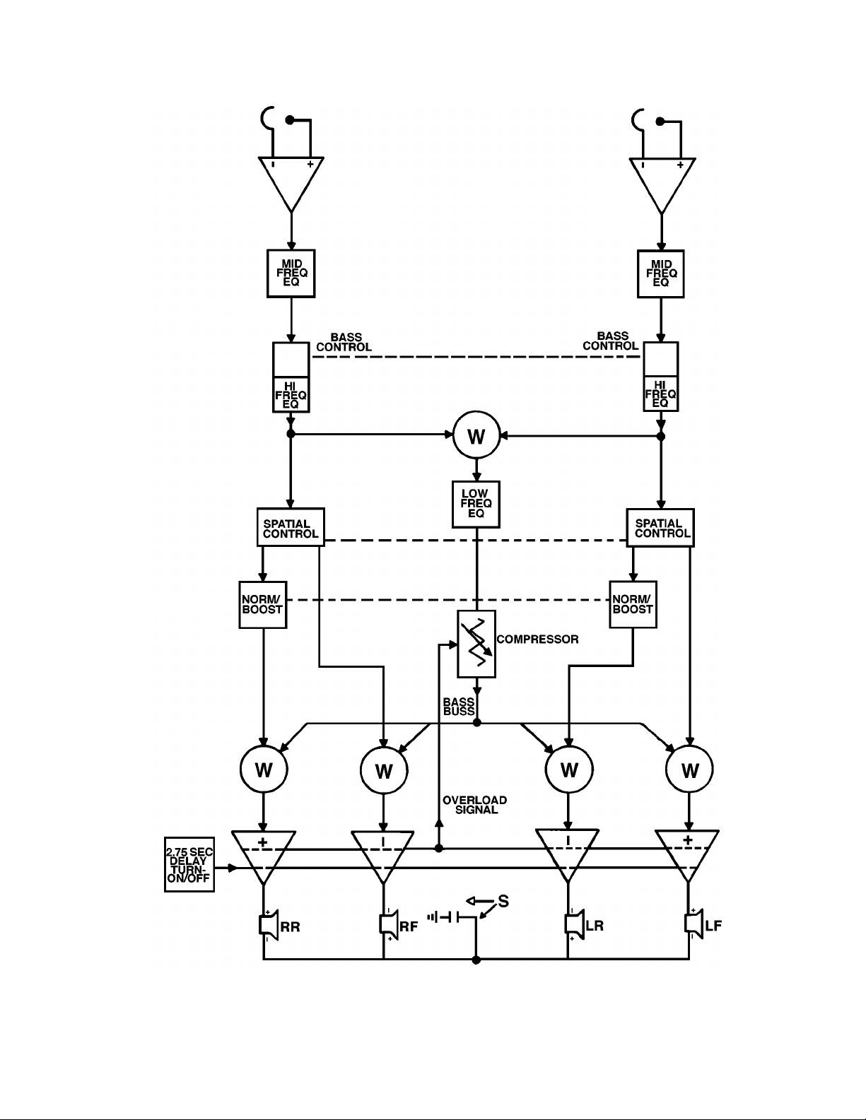
TECHNICAL DESCRIPTION
Figure 1. 1401 Block Diagram
9
Page 10

TECHNICAL DESCRIPTION
Figure 2. 1401 II Block Diagram
10
Page 11

DISASSEMBLY/ASSEMBLY PROCEDURES
Note: The following procedure is for the
1401™ series II. The disassembly for the
1401 series I is the same with the exception of the earlier units.
1. Bottom Cover Removal
4.2 Secure the top cover to the PCB
assembly using the three screws removed
in procedure 3.3.
Note: Be sure to use the plastic washers
when replacing the screws.
1.1 Turn the unit over onto its top.
1.2 Remove the four screws that secure
the bottom cover to the heatsinks.
1.3 Center the slide pot knobs and lift off
the cover.
2. Bottom Cover Replacement
2.1 Place the bottom cover onto the unit
while aligning the slide pot knobs onto the
slide pots.
Note: The 1401 series I has two slide pot
knobs and one power switch knob.
2.2 Secure the bottom cover to the
heatsinks.
3. Top Cover Removal
3.1 Perform procedure 1.
3.2 Remove the two screws located on the
top of the top cover and turn the unit over
onto its top cover.
4.3 Replace the two screws located on the
top of the top cover.
4.4 Perform procedure 2.
Note: The following procedure is for the
1401 series I with serial numbers below
5,000. The serial number is stamped into
the heat sink.
5. Top Cover Removal
5.1 Perform procedure 1.
5.2 Remove the single phillips head screw
and nut that is nearest to the back of the
1401. This holds the PCB to the cover.
5.3 Remove the remaining three phillips
screws and nuts that hold the Delay Turn
On/Off board to the main board.
Note: Make note of the position of the
small spacers. There are also three longer
spacers located under the Delay Turn On/
Off PCB.
3.3 Locate and remove the three screws
securing the top cover to the PCB.
One screw is located near the center of the
PCB, another screw is located at the right
side edge of the front panel, and the other
is located at the rear of the unit holding the
harness clamp in place.
3.4 Lift the PCB away from the top cover
assembly.
4. Top Cover Replacement
4.1 Place the PCB assembly onto the top
cover.
5.4 Remove the two screws that hold the
top cover to the PCB assembly.
5.5 Lift the top cover from the PCB
assembly.
6. Top Cover Replacement
6.1 Place the top cover on to the PCB and
secure it to the heatsink.
6.2 Replace the three phillips screws and
align the spacers with the Delay Turn On/
Off PCB.
6.3 Replace the screw and nut at the back
of the unit and perform procedure 2.
11
Page 12

DISASSEMBLY/ASSEMBLY PROCEDURES
1. Bottom Cover Removal
1201 Disassembly/Assembly Procedure
3.3 Remove the four screws securing the
PCB to the heat sink.
1.1 Remove the four screws located at the
back (connector end) of the unit and the
two screws located at the front of the unit.
1.2 Remove the bottom cover.
2. Bottom Cover Replacement
2.1 Place the bottom cover onto the unit.
2.2 Secure the cover to the heatsink.
3. PCB Removal
3.1 Perform procedure 1.
3.2 Remove the plastic insulator from the
PCB.
3.4 Lift the PCB assembly off of the heat
sink.
4. PCB Replacement
4.1 Place the PCB assembly onto the heat
sink.
Note: Make sure that the output transistor's
insulator is in its proper position and is not
misaligned.
4.2 Secure the PCB to the heat sink.
4.3 Perform procedure 2.
12
Page 13

TEST PROCEDURES
Test Procedure Set-Up (refer to the diagram below)
Caution: Before connecting the Booster/
Equalizer to the power supply, test the
zener diode for a possible short by checking the resistance between the power and
ground wires. Set your Ohmmeter to the x1
scale. Connect the leads of the meter to the
red and black wires. In one direction (red to
red, black to black) you should get a reading of infinity . In the other direction (red to
black and black to red) you should get
about .6 ohms for a reading.
Note: The Booster/Equalizer has four
separate amplifiers, two of which are 180º
out of phase with the remaining two amplifiers. Also, the outputs are returned through
the Booster/Equalizer's Speaker Reference. It is important to connect the unit as
directed to prevent damage to the 1401
series I, or activation of the current protection circuits in the 1401 series II, and 1201.
DO NOT connect speaker returns to
ground!!
1401 II/1201 Power Wire Connection
Red wire is B+, Black wire is ground,
Purple wire is Switched B+, and the Brown
wire is Audio ground.
1401 I Speaker Wire Connection
Left Front
1. Output: White/Yellow
2. Return: White/Blue
Right Front
1. Output: White/Green
2. Return: White/Orange
Left Rear
1. Output: Gray/Blue
2. Return: Gray/Yellow
Right Rear
1. Output: Gray/Orange
2. Return: Gray/Green
1401 II/1201 Speaker Wire Connection
Left Front
1. Output: Yellow
2. Return: White
Right Front
1. Output: Green
2. Return: Orange
Left Rear
1. Output: Blue
2. Return: Yellow
Right Rear
1. Output: Orange
2. Return: Gray
13
Page 14

TEST PROCEDURES
Note: The Booster/Equalizer should be
operated and tested using a 100 Ohm load
for each of the speaker outputs until the
unit functions properly. Center the bass
control and Spatial Control™.
1. Initial Turn-On Test
1.1 Connect the speaker to 100 Ohm loads
and connect the power harness to a power
supply at 13.8 Vdc.
1.2 Turn on the power supply and check
the current draw. If the unit is drawing more
than 250 mV shut off the power supply and
check the outputs for shorts.
Note: On the 1401 II and the 1201 if the
unit shuts off and than tries to turn on
approximately every 3 seconds the outputs
could be shorted.
1.3 Apply a 125 mV 1 kHz signal to the low
level inputs and adjust the Spatial Control
to electronically center (the front and rear
output should be the same amplitude).
2. Low Frequency Response Test
2.1 Apply a 35 mV 1 kHz signal to the low
level inputs.
2.2 Reference a dB meter to the output of
the Booster/Equalizer.
2.3 Apply a 35 mV 100 Hz signal and slide
the low frequency control to the minus (-)
side. There should be a -6.5 dB ±1 dB
decrease in output.
2.4 Center the control. Reference a dB
meter to the output of the Booster/Equalizer.
2.5 Slide the control to the plus (+) side.
There should be a +6.5 dB ±1 dB increase
in output.
3. Spatial Control, High Frequency, and
Rear Switch Control Test
3.1 Apply a 35 mV 15 kHz signal to the low
level inputs.
3.2 Reference a dB meter to the output of
the Booster/Equalizer.
3.3 Slide the spatial control to maximum
right (front speakers). There should be a +1
dB ±1 dB increase in output and a -30 dB
cut to the rear speakers.
3.4 Slide the spatial control to maximum
left (rear speakers). There should be a +1
dB ±1 dB increase in output and a -30 dB
cut to the front speakers.
3.5 Center the spatial control and switch
the rear high frequency switch to position I.
The rear output should be -10.5 dB ±1 dB
from the front output.
3.6 Return the rear high frequency switch
to position II.
4. Power and Distortion Test
Note: Refer to the diagram on page 14 for
the schematic diagram of the .45 Ohm
load.
4.1 Connect the speaker outputs to .45
Ohm loads.
4.2 Apply a 1 kHz signal to the low level
inputs and increase the input until the
output signal just begins to clip. The
output reading should be approximately
3.36 Volts.
4.3 Decrease the applied signal until the
output reads 3.20 Volts. The distortion
should be .09% for all four channels.
Note: The length and size of the wiring
and the connection to the load is very
important. Make sure the connections are
as tight as possible to achieve correct
distortion readings.
14
Page 15

TEST PROCEDURES
5. High Level Input Test
5.1 Apply a 1 kHz signal to the high level
inputs.
5.2 Increase the input level until the output
just begins to clip. The signal input reading
should be approximately 2.75 Volts.
6. Protection Circuit Test
Note: This test is for the 1401 II and the
1201 only. Signal is applied to the low level
input.
6.1 Apply a 1 kHz signal so the output of
the unit is approximately 1.50 Volts.
6.2 Short anyone of the outputs to ground.
The unit should immediately shut down and
then try to turn on every three seconds.
6.3 Remove the short. The unit should turn
on and operate properly without damage to
the channel that had been shorted.
15
Page 16

PART LIST NOTES
1. This part is not normally available from Customer Service. Approval from the Field Service
Manager is required before ordering.
2. The individual parts located on the PCBs are listed in the Electrical Parts Lists.
3. The reference designators in bold are found in the 1401™ PCB's with serial numbers below
5,000.
4. The reference designators in bold are found in the 1201 only. All other reference designators
are common to both the 1401 II and the 1201.
5. This item is not shown. The item is used with the 1401 II using 6"x 9" speakers (large
vehicle systems).
PCB IDENTIFICATION
1401 series I PCB Layout View
1401 series II PCB Layout View
16
Page 17

Figure 3. 1401™, 1401 II, and 1201 Exploded View
17
Page 18

Figure 4. Main Part List Exploded View
18
Page 19

MAIN PART LIST
(Refer to Figures 3 and 4)
Item Number Description Part Number Qty. Note
1 Dpdt Slide Switch 112553 1 or 2
2 4 Pin Connector 112738-4 1
3 Phone Jack 110386 2
4 Heat Sink, Driver Transistor 112733 8
5 Main Heat Sink 114276 2 1401
6 Screw, #4-40 x .25L Self Tap TORX 112650-04 8
6 Washer, Shoulder 113437 8
6 Insulator TO-220 112564 8
7 Ext. Tooth #6 Lock Washer 108261-06 2
8 LED Assembly Green 112614 1
9 Power Switch 112086 1 1401
10 Potentiometer 123408 1 1201
11 Front Panel 111997 1
12 Front Panel, Heatsink 118975 1 1401 II
13 1201 Heatsink 123120 1 1201
14 Screw, Hold Down 103140-04 2 1201
14 Nut, Hold Down 121710-04 2 1201
15 Transistor, Hold Down 123431 1 1201
16 Output, Harness Assy 123733 1 1201
16 Front Speaker Output Assy 121795 1 1401 II
16 Rear Speaker Output Assy 121796 1 1401 II
16 Power Cable Assy, Amp 119218 1 1401 II
17 Case, 1401 114521 1
17 Speaker, Output Assy 123731 1
18 Harness Assembly, Amp 112761 1 1401
19 Zinc Cover 114586 1
20 Knob 111994 2 or 3
21 1201 Cover 123381-1 1 1201
22 Support Bracket 112501 1
23 Angle Bracket 112502 2
23 AmpIifier Accy Kit, Mounting 119303 1
24 Input Wire Assembly 123750 1
25 Ground Wire Assembly 112760 1 1401
26 Power Wire Assembly 112579 1 1401
27 Power Cable (auto) 119215 1 1401 II
28 Front Speaker Cable Assy 121794 1 1401 II
28 Rear Speaker Cable Assy 119220 1 1401 II
--- Speaker Wiring Assy, Front and Rear 112745 1 1401
--- PC Mounting Strip 123465 1 1201
--- Screw, #6 Sheet Metal, Torx .5 Lg 107488-08 6
--- Screw, #4 Tap-Tite, Torx .5 Lg 122993-08 3
--- Transistor Insulator 122920 2
--- PC Insulator 123753 2 1201
-- - Dust Cover 123858 2 1201
19
Page 20

ELECTRICAL PART LIST
1401 Series I
Resistors
Reference Designator Description Part Number Note
R1 1K, 1/2W, 5%, CF 113777-102
R2, 3, 70, 90 150K, 2%, CF 107182-154 3
R4 10 Ohm, 5%, CF 103774-100
R10, 40, 77, 83 5.6K, 2%, CF 113773-562 3
R11, 21, 31, 41 910 Ohm, 5%, CF 107183-911
R12, 42 1 1K, 2% , C F 113773-113 3
R13, 43 220 Ohm, 5%, CF 113774-221
R14, 24, 34, 44, 86 47 Ohm, 5%, CF 107183-470
R15, 16, 25, 26, 36, 45, 46 27 Ohm, 5%, CF 113774-270 3
R16, 35, 45, 46 27 Ohm, 5%, CF 107183-270
R17, 18, 27, 28, 37, 38, 47,48.5 Ohm, 1.6W, 5%, WW 112737-OR5
R19, 22, 29, 32, 39, 49, 94,
159
R19A,19B, 29A, 29B,
39A, 39B, 49A, 49B
R20, 30 3K, 5%, CF 107183-302
R20, 30, 62, 71, 79, 87,
111, 114
R23, 33 220 Ohm, 5%, CF 107183-221
R32 18K, 2%, CF 113773-183
R40, 69, 105 5.6K, 2%, CF 107182-562
R42 11K, 2%, CF 107182-113
R50 510 Ohm, 5%, CF 107183-511
R51, 53 47K, 5 %, C F 107183-473
R52, 59, 71, 107 15K, 2%, CF 107182-153 3
R53, 60, 67, 73, 88, 99,
104, 110, 117-124
R55 2 Ohm, 5%, CF 107183-2RO
R56, 62, 63, 75, 76, 87, 88,
91, 92, 93, 99, 100, 101,
102, 108, 111, 113, 114,
150
R57, 58, 85, 155 24K, 5%, CF 107183-243 3
R52, 59, 61, 95, 96, 98,
104, 105
R60, 68, 97 20 Ohm, 1W, 5%, CC
R54, 61, 70, 84, 106 200K, 2%, CF 107182-204 3
R63, 67, 75, 76, 81, 82,
115, 116
R64, 65, 90, 91, 98, 101,
103, 102
R66, 89, 93, 100, 103 12K, 2%, CF 107182-123 3
R69, 89, 92, 151 62K, 2%, CF 107182-623 3
R72, 108, 109, 110 8.2K, 2%, CF 107182-822 3
R77, 78, 81, 112 2K, 2%, CF 107182-202 3
R78, 79, 82, 83, 113, 153 1.3K, 2%, CF 107182-132 3
R84, 157 1M, 5%, C F 113774-105 3
18K, 2%, CF 107182-183 3
4.7K, 5%, CF 113774-472 3
3.3K, 2%, CF 107183-332 3
4.7K, 2%, CF 107182-472 3
10K, 2%, CF 107182-103 3
100K, 2%, CF 107182-104 3
104064-200
20 Ohm, 1W, 5%, CF (Alt)
6.8K, 2%, CF 107182-682 3
51K, 2%, CF 107182-513 3
107163-200
3
20
Page 21

ELECTRICAL PART LIST
1401 Series I
Resistors (continued)
Reference Designator Description Part Number Note
R95 330K, 5%, CF 113774-334
R158 12K, 2%, CF 113773-123 3
R201, 208 47K, 5%, C F 113774-473 3
R202 220K, 5%, CF 113774-224 3
R203, 209 22K, 5%, CF 113774-223 3
R205 1 Ohm, 5%, CF 113774-103 3
R206 2 Ohm, 5%, CF 113774-2RO 3
R207 100K, 5%, CF 113774-104 3
R210 510 Ohm, 5%, CF 113774-511 3
Capacitors
Reference Designator Description Part Number Note
C1, 61, 63, 69, 72, 77, 79 .01uF, 25V, 20%, Cer Disc 102399
C2 330uF, 16V, Electrolytic 113173
C3, 52, 61, 64, 65, 85, 201 10uF, 25V ,Electrolytic 106777 3
C4 4700uF, 18V, Electrolytic 112555
C11, 21, 31, 41 680pF ,100V ,10%, Cer
Disc
C12, 42 43pF, 200V, 10%, Cer Disc 104413-430
C13, 15, 23, 25, 33, 35, 43,451800pF, 100V, 10%, Cer
Disc
C14, 24, 34, 44 1000uF, 16V, Electrolytic 112554
C22, 32 27pF, 200V, 10%, Cer Disc 104413-270
C51, 58, 79 0.12uF, 50V, 5%, Film 114036
C52, 60 .0056uF, 50V, 5%, Film 106537-561
C54, 55, 62, 70, 71, 73-75,
76, 81, 82, 83, 152
C53, 202 10uF, 25V, Tantalum 114035 3
C51, 64, 84, 203 .0056uF, 50V, 5%, Film 114037
C56, 60, 66, 68, 69, 73, 74,
76, 80
C55, 57, 62, 65, 66, 67, 72,
78, 86, 150
C53, 59, 81 560pF, 100V, 5%, Film 106537-561 3
C67, 151 75pF, 50V, 10%, Cer Disc 114412-750 3
C68, 153 1500pF, 50V, 10%, Cer
C57, 70 .047uF, 50V, 5%, Film 112797 3
1uF, 25V, Electrolytic 104015 3
.01uF, 50V, 5%, Film 112774 3
.022uF, 50V, 5%, Film 112772 3
Disc
106541-681
106542-182
106542-152 3
Diodes
Reference Designator Description Part Number Note
D2 IN5355B (Zener 18V/5W)
IN5355B (Zener 18V/5W)
D11-13, 21-23, 31-33, 41-
43, 50, 52, 201
D51, 202 IN5240B (Zener) 114058
Zl, 50 CLM-6000 (Opto Isolator) 112540
IN4148 114048
21
122893
120559 ALT.
Page 22

ELECTRICAL PART LIST
1401 Series I
Transistors
Reference Designator Description Part Number Note
Q11, 21, 31, 41 NSD U51, PNP 112998
Q12, 22, 32, 42, 53, 202 MPS U01, NPN 112999
Q13, 23, 33, 43 D44H2 119893
Q14, 24, 34, 44 D45H2 119892
Q15, 25, 35, 45, 50, 201 2N3906 102426
Q16, 26, 36, 46, 52, 54,
203, 205
Q51, 204 National MPSA13 114282
Reference Designator Description Part Number Note
U11, 21, 31, 41 Integrated Amp NE538N 123128
U50, 201 Integrated 555 114012
U51 Dual Op Amp 4559 108568
U52, 53 Quad Op Amp TLO74CN 112996
2N3904 102432
Integrated Circuits
22
Page 23

ELECTRICAL PART LIST
1401 Series II and 1201
Resistors
Reference Designator Description Part Number Note
R11, 12, 21, 22, 31, 32, 41,42.47 Ohm, 5%, CF 108904
R13, 14, 23, 24, 33, 34, 43,
44, 125, 126, 225, 226
R15, 25, 35, 45, 129, 229 220 Ohm, %5, CF 117704-1212215 4
R16, 26, 36, 46, 130, 230 47 Ohm, 5%, CF 117704-1214705 4
R17, 37 11K, 1%, MF 119976-2211102
R18, 28, 38, 48, 121, 141,
221
R27, 47, 103, 222 17.8K, Ohm, 1%, MF 119976-2211782 4
R51, 71, 103, 203 20 Ohm, 1W, 5% 104064-200 4
R52, 53, 72, 73, 101, 102,
112, 113, 115, 201, 202,
516, 517
R54, 55, 66, 74, 75, 86,
104, 105, 115, 204, 205,
215, 513
R56, 57, 76, 77 51.1K, 1%, MF 119976-2225112
R58 12.1K, 1%, MF 119976-2221212
R59, 64, 79, 84 4.75 Ohm, 1%, MF 119976-2224751
R60, 80, 105, 107 5.62K, 1%, MF 119976-2215621
R61, 81 200K, 1%, MF 119976-2212003
R63 15K, 1%, MF 119976-2221502
R65, 85 8.25K, 1%, MF 119976-2218251
R67, 87 3.32K, 1%, MF 119976-2213321
R68, 88, 117, 217, 305 2.00K, 1%, MF 119976-2212001 4
R69 1.30K, 1%, MF 119976-2211301
R78, 110, 210, 514 12.1K, 1%, MF 119976-2211212 4
R82, 110 1K, 5%, CF 117704-1211025
R83, 112, 212, 119, 122 15K, 1%, MF 119976-2211502 4
R86 10K, 1%, MF, 1/4W 119976-2221002
R88 2K, 1%, MF 119976-2222001
R89 1.3K, 1%, MF 119976-2221301
R90, 116, 216 39.2K, 1%, MF 119976-2213922 4
R91 39.2K, 1%, MF 119976-2223922
R92 61.9K, 1%, MF 119976-2226192
R93 150K, 1%, MF 119976-2221503
R94, 97, 150 6.81K, 1%, MF 119976-2216811
R95, 96 6.81 Ohm, 1%, MF 119976-2226811
R101, 102, 104 17.8K, 1%, MF 119976-2221782
R106 3.01K, 1%, MF 119976-2213011
R106, 107, 206, 207 25.5K, 1%, MF, 1/4W 119976-2212552 4
R108 3.01K, 1%, MF 119976-2223011
R108, 208 24.9K, 1%, MF, 1/4W 119976-2212492 4
R109 75.5K, 1%, MF, 1/4W 119976-2217502 4
R111 10 Ohm, 5%, CF 117704-1211005
R111, 211 4.75K, 1%, MF, 1/4W 119976-2214751 4
R113 100K, 1%, MF 119976-2211003
R113, 213 8.25K, 1%, MF, 1/4W 119976-2218251 4
R114 33.2K, 1%, MF 119976-2223322
R114, 214 4.32K, 1%, MF, 1/4W 119976-2214321 4
27 Ohm, 5%, CF 117704-1212705 4
910 Ohm, 5%, CF 117704-1219115 4
100K, 1%, MF 119976-2221003 4
10K, 1%, MF, 1/4W 119976-2211002 4
23
Page 24

ELECTRICAL PART LIST
1401 Series II and 1201
Resistors (continued)
Reference Designator Description Part Number Note
R116, 121-123, 503, 504,
601
R117, 126-128, 301, 303,
401, 403, 507, 510, 604,
605
R118 360 Ohm, 5%, CF 117704-1223615
R118 2.32K, 1%, MF, 1/4W 119976-2212321 4
R119 560 Ohm, 5%, CF 117704-1225615 4
R120 1.8K, 5%, CF 117704-1221825
R120, 220 6.19K, 1%, MF, 1/4W 119976-2216191 4
R123, 124, 223, 224, 522 4.7K, 5%, CF, 1/4W 117704-1214725 4
R124 220K, 5%, CF 117704-1212245
R125 18 Ohm, 5%, CF 117704-1211805
R127, 128, 227, 228 .47 Ohm, 5%, 2W 123355 4
R129-136 4.7K, 5%, CF 117704-1214725
R131, 231 7.15K, 1%, MF, 1/4W 119976-2217151 4
R137, 139 .03 Ohm, 2W, 10% 119748
R142 2.2 Ohm, .5W, 1%, MF 113777-2R2
R145, 146, 512 560 Ohm, 5%, CF 117704-1215615 4
R209 75.0K, 1%, MF, 1/4W 119976-2227502 4
R218 4.99K, 1%, MF, 1/4W 119976-2214991 4
R219, 519 18.2K, 1%, MF, 1/4W 119976-2211822 4
R302, 402 2.7K, 5%, CF, 1/4W 117704-1212725 4
R304, 404 51K, 5%, CF, 1/4W 117704-1215135 4
R405 1.82K, 1%, MF, 1/4W 119976-2211821 4
R501 61.9K, 1%, MF, 1/4W 119976-2216192 4
R502 150K, 1%, MF, 1/4W 119976-2211503 4
R505 10 Ohm, 5%, CF, 1/4W 117704-1211005 4
R506, 508, 509 15K, 5%, CF, 1/4W 117704-1211535 4
R511 .03 Ohm, 10%, 2W 119748 4
R515 29.4K, 1%, MF, 1/4W 119976-2212942 4
R518 332, Ohm, 1%, MF, 1/4W 119976-2213320 4
R520 1.2K, 5%, CF, 1/4W 117704-1211225 4
R521 470 Ohm, 5%, CF, 1/4W 117704-1214715 4
R602 5.1K, 5%, CF, 1/4W 117704-1215125 4
R603 91K, 5%, CF, 1/4W 117704-1219135 4
47K, 5%, CF 117704-1214735 4
10K, 5%, CF 117704-1211035 4
24
Page 25

ELECTRICAL PART LIST
1401 Series II and 1201
Capacitors
Reference Designator Description Part Number Note
C11, 21, 31, 41, 113, 213 1000uF, 16V, Electrolytic 120970
C12, 13, 22, 23, 32, 33, 42,
43, 110, 111, 210, 211
C14, 34 43pF, 50V, 10%, Tubular 117245-430107
C15, 25, 35, 45, 101, 102 680pF, 50V, 10%, Tubular 119274-681102
C24, 44 27pF, 50V, 10%, Tubular 117245-270107
C51, 93, 97-100 112, 212,
507
C52, 92 10uF, 25V, 20%, Elec., LL
C53 4700uF, 16V, Electrolytic 119198
C61, 62, 71, 72, 81, 82 1uF, 50V, Elec., Low Leak 119942-1R0
C63, 94, 103 .01uF, 25V, 20%, Tubular 119273-103201
C64, 74, 95, 96 .022uF, 100V, 5%, Film 118091-223
C65, 67, 75, 77, 84, 503 .01uF, 100V, 5%, Film 118091-103 4
C66, 76 0.12uF, 100V, 5%, Film 120388-124
C68, 78 560pF, 50V, 5%, Disc 119272-561
C69, 79, 107, 207 .0056uF, 100V, 5%, Film 118091-562 4
C83 .082uF, 100V, 5%, Film 118091-823
C85, 502 .047uF, 100V, 5%, Film 118091-473 4
C86 .47uF, 50V, Electrolytic 119943-R47
C87, 88 .47uF, 25V, 10%, Elec., LL 119315
C91, 508 330uF, 16V, Electrolytic 113173 4
C101, 102, 108, 201, 202,
208, 512, 602
C103, 203 33pF, 5%, Disc 119372-330 4
C104, 204, 502 .033uF, 5%, Disc 118091-333 4
C105, 205 0.12uF, 5%, Disc 121503 4
C106, 206 390pF, 5%, Disc 119272-391 4
C109, 209, 509 680pF, 5%, Disc 119272-681 4
C114 43pF, 5%, Disc 119372-430 4
C214 27pF, 5%, Disc 119372-270 4
C301, 501, 506 0.1uF, 5%, Disc 117502 4
C302, 402, 504 .068uF, 5%, Film 118091-683 4
C505 100uF, Electrolytic 120767 4
C510 22uF, Electrolytic 120763-220 4
C511 2200uF, Electrolytic 123409 4
C601 4.7uF, Electrolytic 120763-4R7 4
1800pF, 50V, 10%, Disc 119017-182 4
10uF, 35V, Electrolytic 120763-100 4
119202
10uF, 25V, 20%, Elec., LL
1.0uF, Electrolytic 120763-1R0 4
114035 ALT.
Diodes
Reference Designator Description Part Number Note
D11, 12, 21, 22, 31, 32, 42,
51, 101, 102, 201, 202, 501,
502, 601
D55 High Current Diode 122893
D503 Silicon Diode 120559 4
D504 Zener, 5.6V, 1W 116995-4734A 4
IN4150 121542 4
25
Page 26

SPEAKER PART LIST
(Refer to Figure 5)
Item Number Description Part Number Qty. Note
1 Plain Grille Assy, Grey
Plain Grille Assy, Black
2 Escutcheon (For Deluxe Grille) 1401 111769 1
3 4.5" Driver 119179 1
4
5 Masonite Gasket 112410 1
6 Deluxe Grille - Reflector only 111785 1
7 Grille Assembly, (6"x 9") 123705 1
8 Frame (For Deluxe Grille) 111768 1
9 6"x 9" Driver 123456 1
10 Adapter Plate Kit 112573 1
--- Speaker Mounting Kit 119304 1
--- Speaker, Mounting Kit (6"x 9") 123644 1
--- Owner's, Manual, 1201 123696 1
--- Owner's, Manual, 1401 114733 1
---
--- LFR-069 EQ 124244 1 5
Escutcheon (For Deluxe Grille)1401 II
Owner's, Manual, 1401 II
112023
119548
119511 1
119287 1
1
1
Figure 5. Speaker Exploded View
26
Page 27

TECHNICAL INFORMATION
27
Page 28

TECHNICAL INFORMATION
Trouble Shooting Guide
Symptom Check
Draws current:
No left or r i g h t o u t p u t : Check electrolytic caps at the input to U51 or at the output
Spatial not working:
Drivers running hot: Check the bias diodes D11, 12, 21, 22, 31, 32, 41 and 42.
No output one channel only or unit
cycles on and off:
Unit will not turn on: 1: Outputs should not be grounded. Isolate test
No output or cycles on and off after
installing new outputs and drivers:
No low frequencies: Check U53
Check D55, series II; Check D2, series I
of U52 for series I and U53 for series II. Replace all caps
with a silver colored can.
Check C88, C87 series II, C65, C85 series I
1: Check output and drivers; Replace both outputs, both
drivers and both bias diodes, if one is found defective.
Check the 27Ω resistors connected to bias diodes.
2: Check Q54 and Q55 for series II.
equipment from ground.
2: Check Q62, Q63, U52 for series II. Check Q51, Q54,
U50 for series I.
3: Check D51, R120, Q53. Make sure the remote turn on
violet wire is connected to power, series II.
Check for cracked screw insulators and make sure that the
insulator between transistors and heat sink is good.
28
Page 29

29
Page 30

SPECIFICATIONS AND FEATURES SUBJECT TO CHANGE WITHOUT NOTICE
®
®
Bose Corporation
The Mountain
Framingham Massachusetts USA 01701
P/N 122762 REV. 01 12/98 FOR TECHNICAL ASSISTANCE OR PART ORDERS, CALL 1-800-367-4008
 Loading...