


INSTRUCTION MANUAL
MODEL 1121A
PROGRAMMABLE
AUDIO ANALYZER
REV DATE 05/16
MANUAL P/N 98407600A
Wireless Telecom Group
25 EASTMANS ROAD, PARSIPPANY, NJ 07054
Telephone: 973-386-9696
Fax: 973-386-9191
Email: boonton@boonton.com
Web: www.wtcom.com

This page intentionally blank.
SAFETY SUMMARY
The following general safety precautions must be observed during all phases of operation and maintenance of this
instrument. Failure to comply with these precautions or with specific warnings elsewhere in this manual violates
safety standards of design, manufacture, and intended use of the instrument. Boonton Electronics assumes no liability
for the customer’s failure to comply with these requirements.
THE INSTRUMENT MUST BE GROUNDED
To minimize shock hazard the instrument chassis and cabinet must be connected to an electrical ground. The
instrument is equipped with a three conductor, three prong power cable. The power cable must either be plugged into
an approved three-contact electrical outlet or used with a three-contact to a two-contact adapter with the (green)
grounding wire firmly connected to an electrical ground at the power outlet.
DO NOT OPERATE THE INSTRUMENT IN AN EXPLOSIVE ATMOSPHERE
Do not operate the instrument in the presence of flammable gases or fumes.
KEEP AWAY FROM LIVE CIRCUITS
Operating personnel must not remove instrument covers. Component replacement and internal adjustments must be
made by qualified maintenance personnel. Do not replace components with the power cable connected. Under certain
conditions dangerous voltages may exist even though the power cable was removed; therefore, always disconnect
power and discharge circuits before touching them.
DO NOT SERVICE OR ADJUST ALONE
Do not attempt internal service or adjustment unless another person, capable of rendering first aid and resuscitation, is
present.
DO NOT SUBSTITUTE PARTS OR MODIFY INSTRUMENT
Do not install substitute parts or perform any unauthorized modification of the instrument. Return the instrument to
Boonton Electronics for repair to ensure that the safety features are maintained.
SAFETY SYMBOLS
This safety requirement symbol (located on the rear panel) has been adopted
by the International Electrotechnical Commission, Document 66 (Central
Office) 3, paragraph 5.3, which directs that the instrument be so labeled if, for
the correct use of the instrument, it is necessary to refer to the instruction
manual. In this case it is recommended that reference be made to the
instruction manual when connecting the instrument to the proper power
source. Verify that the correct fuse is installed for the power available, and
that the switch on the rear panel is set to the applicable operating voltage.
The CAUTION sign denotes a hazard. It calls attention to an operation
procedure, practice, or the like, which, if not correctly performed or adhered
to, could result in damage to or destruction of part or all of the equipment. Do
not proceed beyond the CAUTION sign until the indicated conditions are
fully understood and met.
The WARNING sign denoted a hazard. It calls attention to an operation
procedure, practice, or the like, which, if not correctly performed or adhered
to, could result in injury or loss of life. Do not proceed beyond a WARNING
sign until the indicated conditions are fully understood and met.
Indicates dangerous voltages.

This page intentionally blank.

I
Table of Contents
Paragraph Page
SECTION I - GENERAL INFORMATION
1-1. INTRODUCTION ................................................................................................................... 1-1
1-3. DESCRIPTION ...................................................................................................................... 1-1
1-5. ACCESSORIES ..................................................................................................................... 1-1
1-7. OPTIONS ............................................................................................................................. 1-1
1-9. SPECIFICATIONS ................................................................................................................. 1-1
SECTION II - INSTALLATION
2-1. INTRODUCTION ................................................................................................................... 2-1
2-3. UNPACKING ........................................................................................................................ 2-1
2-5. MOUNTING ........................................................................................................................... 2-1
2-7. POWER REQUIREMENTS ................................................................................................... 2-1
2-10. CABLE CONNECTIONS .................................................................................................... 2-1
2-13. PRELIMINARY CHECK ....................................................................................................... 2-2
SECTION III - OPERATION
3-1. INTRODUCTION ................................................................................................................... 3-1
3-3. OPERATING CONTROLS, INDICATORS AND CONNECTIONS ........................................ 3-1
3-5. OPERATING INSTRUCTIONS .............................................................................................. 3-1
3-7 INITIAL CONDITIONS ............................................................................................................ 3-1
3-9. LOCAL OPERATION ............................................................................................................. 3-1
3-10. Function Selection ............................................................................................................... 3-1
3-11. Data Entry Operation ........................................................................................................... 3-1
3-13. Analyzer Measurement Description ..................................................................................... 3-6
3-14. Analyzer Input Description ................................................................................................... 3-6
3-15. Frequency Measurement Function ...................................................................................... 3-6
3-16. Frequency Measurement Display Units ............................................................................... 3-6
3-17. Special Frequency Measurement Modes ............................................................................ 3-6
3-18. Level Measurement Function ............................................................................................. 3-6
3-19. Level Measurement Display Units ....................................................................................... 3-6
3-20. Special Level Measurement Modes ................................................................................... 3-6
3-21. Distortion Measurement Function ........................................................................................ 3-6
3-22. Distortion Measurement Display Units ............................................................................. 3-6
3-23. Special Distortion Measurement Modes .............................................................................. 3-9
3-24. SINAD Measurement Function ............................................................................................ 3-9
3-25. SINAD Measurement Display Units ..................................................................................... 3-9
3-26. Special SINAD Measurement Modes .................................................................................. 3-9
3-27. S/N Measurement Function ................................................................................................. 3-9
3-28. S/N Measurement Display Units .......................................................................................... 3-9
3-29. Special S/N Measurement Modes ....................................................................................... 3-9

II
Paragraph Page
3-30. Using the Ratio Mode .......................................................................................................... 3-9
3-31. Ratio Measurement Display Units ...................................................................................... 3-9
3-32. Using Analyzer Filters ........................................................................................................ 3-10
3-35. Audio Oscillator General Description ................................................................................. 3-10
3-36. Oscillator Output Description ............................................................................................. 3-11
3-37. Source Frequency Display and Selection .......................................................................... 3-11
3-38. Source Frequency Lock Mode Description ........................................................................ 3-11
3-40. Source level Display and Selection .................................................................................. 3-11
3-41. Amplitude Display Units ..................................................................................................... 3-11
3-42. Step Size and Step Key Operation .................................................................................... 3-12
3-43. Increment/Decrement Program Number .......................................................................... 3-12
3-44. Increment/Decrement Frequency Values ........................................................................ 3-12
3-45. Increment/Decrement Level Values ................................................................................... 3-12
3-46. Sweep Mode General Description ..................................................................................... 3-12
3-47. SWEEP Key Description .................................................................................................. 3-12
3-48. START Key Description ..................................................................................................... 3-12
3-49. STOP Key Description ....................................................................................................... 3-12
3-50. X AXIS Output Description ............................................................................................... 3-12
3-51. Y AXIS Output Description ............................................................................................... 3-12
3-53. PEN Output Description ................................................................................................... 3-12
3-54 Using The Sweep Mode .................................................................................................... 3-13
3-56. Generating Frequency Sweeps ......................................................................................... 3-13
3-57. Generating Level Sweeps ................................................................................................ 3-13
3-58. Program Store and Recall Description ............................................................................. 3-13
3-59. Store Operation ................................................................................................................ 3-13
3-60. Recall Operation ................................................................................................................ 3-13
3-61. Program Memory Initialization ........................................................................................... 3-13
3-62. Special Function Description ............................................................................................. 3-13
3-63. Option Switch Functions .................................................................................................... 3-13
3-64. Mode Alteration Function ................................................................................................... 3-14
3-70. Calibration and Test Functions ........................................................................................ 3-18
3-71. S/N Delay Functions .......................................................................................................... 3-18
3-72. Frequency Sweep Resolution Functions ........................................................................... 3-18
3-73. Sweep Rate Functions ..................................................................................................... 3-18
3-74. AC Detector Selection Functions ....................................................................................... 3-18
3-75. Source Impedance Selection Functions ............................................................................ 3-18
3-76. dBV/dBm Display Mode Functions .................................................................................... 3-18
3-77. Option Switch, A4S1, Operation ........................................................................................ 3-18
3-79. Error Codes ...................................................................................................................... 3-18
3-80. REMOTE OPERATION .................................................................................................... 3-18
3-82. Setting the Bus Address ................................................................................................... 3-18
3-83. Entering the Remote Mode ................................................................................................ 3-18
3-84. Returning to Local Mode .................................................................................................. 3-21
3-85. Triggered Operation ........................................................................................................... 3-21
3-86. Talk Operation .................................................................................................................. 3-21
3-87. Talk Status (TS) Mode ....................................................................................................... 3-21
3-88. Talk Value (TV) Mode ...................................................................................................... 3-21
3-89. Talk Program (TP) Mode .................................................................................................. 3-21
3-90. Talk Function (TF) Mode ................................................................................................... 3-21
3-91. Talk Learn (TL) Mode ....................................................................................................... 3-21
3-92. Talk Burst (TB) Mode ......................................................................................................... 3-21
3-93. End-Of-String (EOS) Control ............................................................................................. 3-22
3-94. Using “Service Request” (SRQ) ....................................................................................... 3-22
3-95. Bus Command Responses ................................................................................................ 3-22

III
Paragraph Page
3-96. Program Function Mnemonics ........................................................................................... 3-22
3-97. Number Formatting ............................................................................................................ 3-22
3-98. Data String Format ........................................................................................................... 3-22
3-99. Data String Errors .............................................................................................................. 3-23
3-100. Data String Examples ...................................................................................................... 3-23
3-101. Store and Recall Operation ............................................................................................ 3-23
SECTION IV - THEORY OF OPERATION
4-1. INTRODUCTION ................................................................................................................... 4-1
4-3. FUNCTIONAL BLOCK DIAGRAM ......................................................................................... 4-1
4-14. DETAILED CIRCUIT DESCRIPTION ................................................................................ 4-3
4-15. A11 Power Supply Circuits ................................................................................................. 4-3
4-20. A10 Motherboard Circuits .................................................................................................... 4-5
4-23. A5 CPU Circuits ................................................................................................................... 4-5
4-31. A12 Display and A13 Keyboard Circuits .............................................................................. 4-7
4-35. A4 Frequency Counter Circuits .......................................................................................... 4-7
4-44. A0 Input Circuits ................................................................................................................. 4-8
4-51. A1 Filter Circuits ................................................................................................................. 4-9
4-55. A2 Notch Filter Circuits ...................................................................................................... 4-10
4-61. A3 Detector Circuits ........................................................................................................... 4-11
4-68. A6 Source Circuits ............................................................................................................. 4-13
4-76. A7 Output Circuits ............................................................................................................ 4-14
SECTION V - MAINTENANCE
5-1. INTRODUCTION ................................................................................................................... 5-1
5-3. SAFETY REQUIREMENTS ................................................................................................... 5-1
5-5. REQUIRED TEST EQUIPMENT .......................................................................................... 5-1
5-7. CLEANING PROCEDURE ................................................................................................... 5-1
5-9. REMOVAL AND REPLACEMENT ......................................................................................... 5-1
5-10. Instrument Covers .............................................................................................................. 5-1
5-11. Display/Keyboard Access .................................................................................................. 5-1
5-12. Plug-in Circuit Board ............................................................................................................ 5-3
5-13. Optional Filters ................................................................................................................... 5-3
5-14. Firmware Integrated Circuit .............................................................................................. 5-4
5-15. Component Removal ........................................................................................................... 5-4
5-16. INSPECTION ....................................................................................................................... 5-4
5-18. PERFORMANCE TESTS ................................................................................................... 5-5
5-20. Initial Calibration ................................................................................................................ 5-5
5-21. Analyzer DC Level Accuracy .............................................................................................. 5-5
5-22. Analyzer AC Level Accuracy ............................................................................................... 5-5
5-23. Analyzer Level Flatness ..................................................................................................... 5-6
5-25. Source Impedance Accuracy ............................................................................................... 5-6
5-26. Source Level Accuracy ........................................................................................................ 5-6
5-28. Source Level Flatness ......................................................................................................... 5-6
5-31. Analyzer Low Level AC Accuracy ........................................................................................ 5-7
5-32. Frequency Accuracy ............................................................................................................ 5-7
5-33. Source Frequency Accuracy ................................................................................................ 5-7
5-34. Analyzer Frequency Accuracy ........................................................................................... 5-7
5-35. Low-Pass Filter Accuracy ................................................................................................... 5-8

IV
Paragraph Page
5-37. Residual Distortion and Noise ............................................................................................ 5-8
5-39. Residual Signal-to-Noise Ratio ............................................................................................ 5-8
5-41. Common Mode Rejection Ratio ........................................................................................... 5-8
5-42. Optional Filter Accuracy ....................................................................................................... 5-8
5-43. Optional Filter Test Connections ......................................................................................... 5-8
5-44. 400 Hz High-Pass Filter Accuracy ..................................................................................... 5-10
5-45. AUDIO Band-Pass Filter Accuracy .................................................................................... 5-10
5-46. CCITT Filter Accuracy ...................................................................................................... 5-10
5-47. CCIR Filter Accuracy ........................................................................................................ 5-10
5-48. A, B, and C Weighting Filter Accuracy ............................................................................ 5-10
5-49. C-MESSAGE Filter Accuracy ........................................................................................... 5-10
5-50. ADJUSTMENTS ................................................................................................................ 5-23
5-52. A11 Power Supply Adjustment ......................................................................................... 5-23
5-54. A11R6 Power Fail Adjustment ........................................................................................... 5-23
5-55. A5 CPU Adjustment ........................................................................................................... 5-24
5-57. A5Y1 Timebase Frequency Adjustment .......................................................................... 5-24
5-58. A3 Notch Board Adjustment ............................................................................................. 5-24
5-59. A3R57 Balance and A3R58 Tune Adjustments ............................................................... 5-24
5-60. A0 Input Board Adjustments .............................................................................................. 5-24
5-62. A0R29, A0R12, A0R7 and A0C35 CMRR Adjustments .................................................... 5-24
5-63. A0C5 and A0C32 Flatness Adjustments ........................................................................... 5-25
5-64. A0C10 and A0C33 Flatness Adjustments ......................................................................... 5-25
5-65. A7 Output Board Adjustments .......................................................................................... 5-25
5-66. A7R21, A7R17, and A7R15 Adjustments ........................................................................ 5-25
5-67. A6 Source Board Adjustments ........................................................................................... 5-25
5-68. A5R23 Output Level Adjustment ...................................................................................... 5-25
5-69. A37 CCIR, CCIR/ARM Filter Board Adjustment .............................................................. 5-26
5-71. A37R11 CCIR Cal Adjustment ......................................................................................... 5-26
5-72. TROUBLESHOOTING ..................................................................................................... 5-26
5-76. TROUBLE LOCALIZATION ............................................................................................... 5-26
5-78. Special Diagnostic Function Codes ................................................................................... 5-26
5-79. DAC Test Code .................................................................................................................. 5-26
5-82. Counter Plug-in Board Test .............................................................................................. 5-27
5-83. Input and Filter Plug-in Board Test .................................................................................. 5-27
5-84. Notch and Detector Plug-in Board Test ........................................................................... 5-27
5-85. PREPARATION FOR SHIPMENT ................................................................................... 5-27
5-86. Use of Shipping Case or Containers ................................................................................ 5-27
5-87. Packaging .......................................................................................................................... 5-27
5-88. Storage .............................................................................................................................. 5-27
SECTION VI - PARTS LIST
6-1. INTRODUCTION ................................................................................................................... 6-1
SECTION VII - SCHEMATIC DIAGRAMS

V
LIST OF TABLES
Table Page
TABLE 1-1. PERFORMANCE SPECIFICATIONS ....................................................................... 1-2
TABLE 1-1. PERFORMANCE SPECIFICATIONS CONTINUED ............................................... 1-3
TABLE 1-1. PERFORMANCE SPECIFICATIONS CONTINUED ............................................... 1-4
TABLE 1-1. PERFORMANCE SPECIFICATIONS CONTINUED ............................................... 1-5
TABLE 2-1 INITIAL CONDITIONS .............................................................................................. 2-2
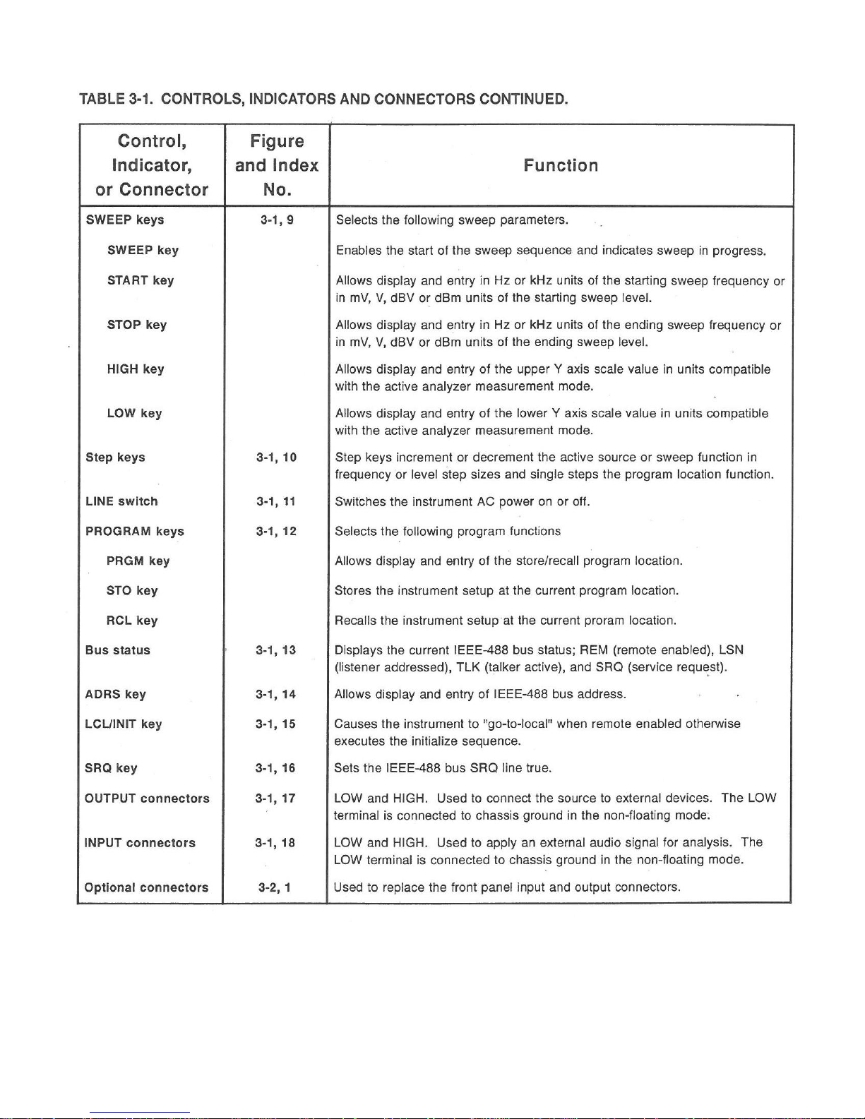
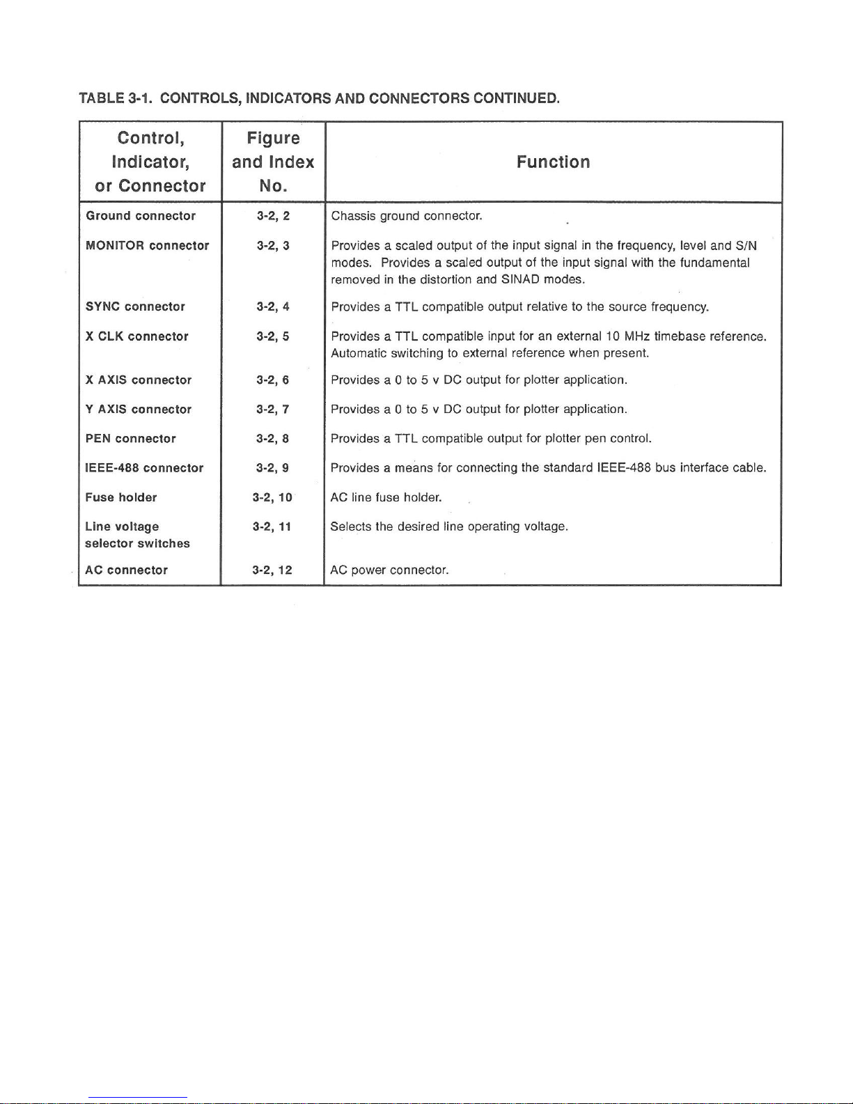
TABLE 3-1. CONTROLS, INDICATORS AND CONNECTORS ................................................... 3-3
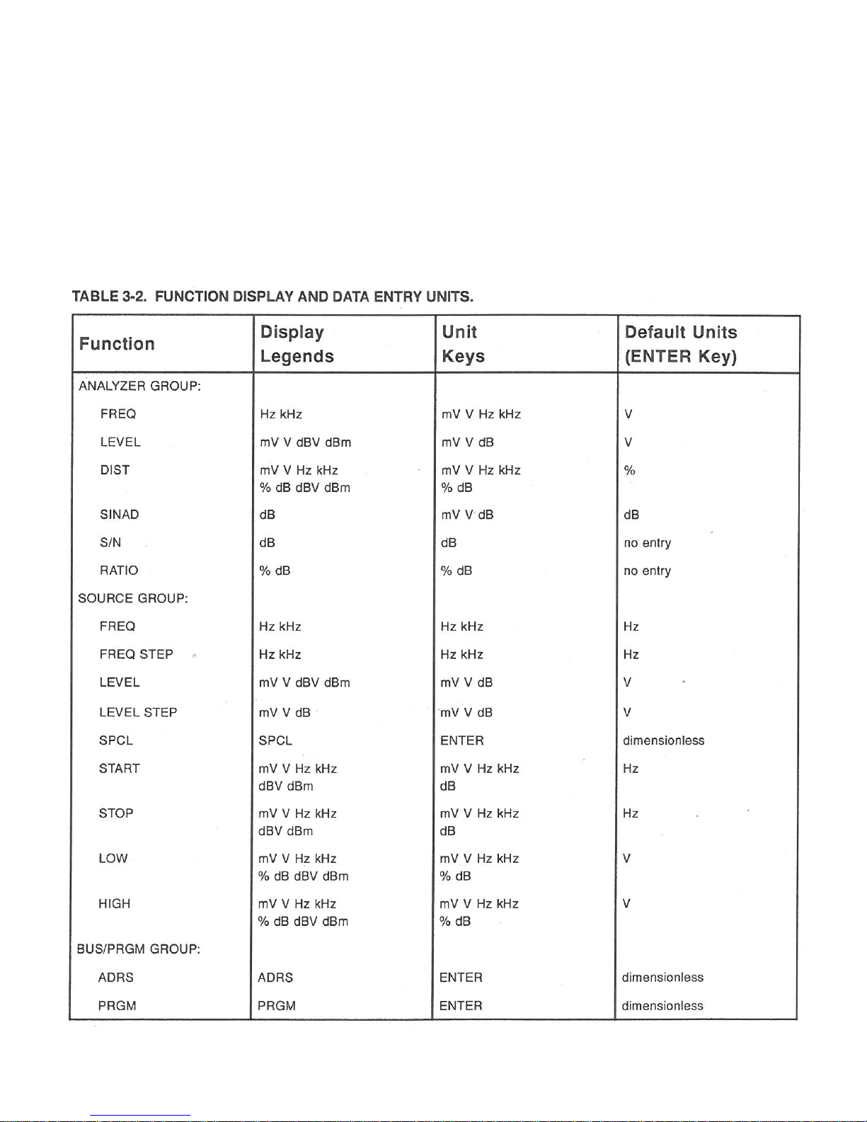
TABLE 3-2. FUNCTION DISPLAY AND DATA ENTRY UNITS ................................................... 3-7
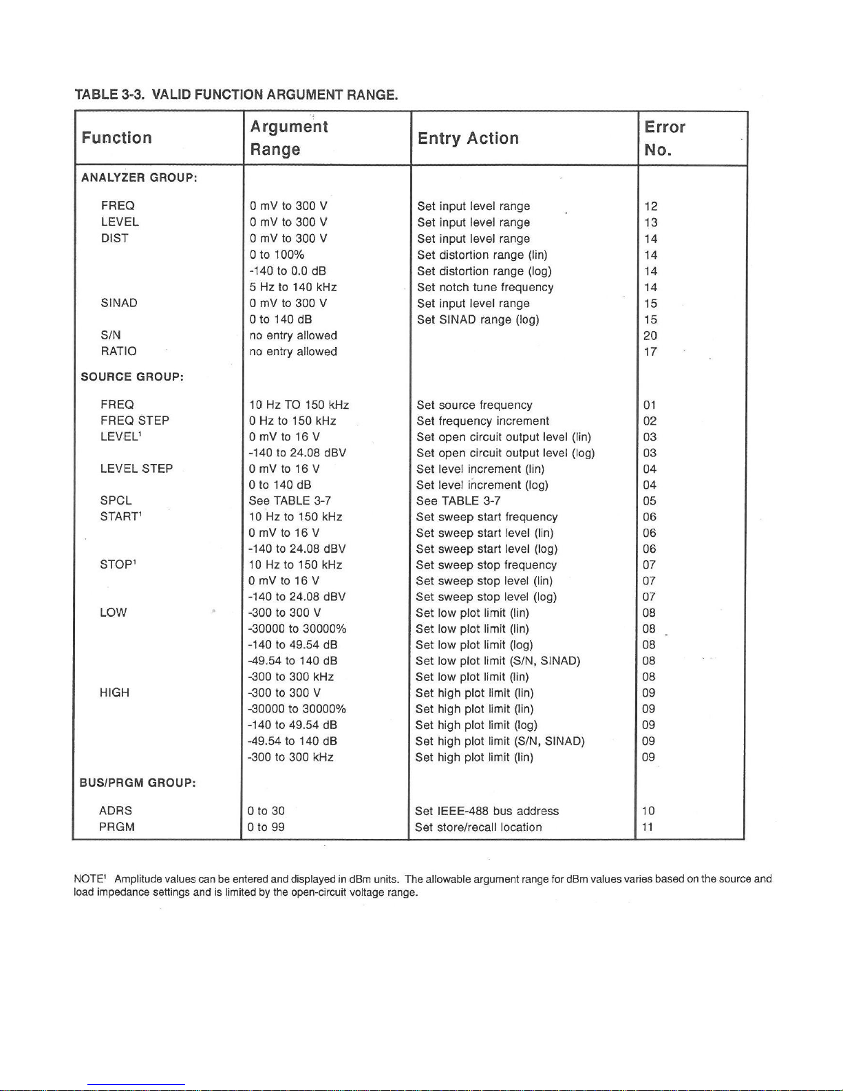
TABLE 3-3. VALID FUNCTION ARGUMENT RANGE ................................................................. 3-8
TABLE 3-4. INPUT LEVEL RANGES ......................................................................................... 3-10
TABLE 3-5. DISTORTION AND SINAD RANGES ..................................................................... 3-11
TABLE 3-6. OUTPUT LEVEL RANGES ..................................................................................... 3-14
TABLE 3-7. SPECIAL FUNCTIONS ........................................................................................... 3-15
TABLE 3-8. OPTION SWITCH A4S1 .......................................................................................... 3-16
TABLE 3-9. ERROR CODES ...................................................................................................... 3-17
TABLE 3-10. IEEE-488 BUS MNEMONICS .............................................................................. 3-19
TABLE 3-11. TALK FUNCTION (TF) DECODING .................................................................... 3-20
TABLE 3-12. BUS COMMAND RESPONSES............................................................................ 3-22
TABLE 5-1. RECOMMENDED TEST EQUIPMENT ................................................................... 5-2
TABLE 5-2. OPTIONAL FILTERS ................................................................................................ 5-3
TABLE 5-3. ANALYZER DC LEVELACCURACYTEST RECORD ............................................... 5-9
TABLE 5-4. ANALYZER AC LEVEL ACCURACY TEST RECORD ......................................... 5-11
TABLE 5-5. ANALYZER AC LEVEL FLATNESS TEST RECORD ............................................ 5-12
TABLE 5-6. SOURCE IMPEDANCE ACCURACY TEST RECORD ......................................... 5-13
TABLE 5-7. SOURCE LEVEL ACCURACY TEST RECORD ..................................................... 5-13
TABLE 5-8. SOURCE LEVEL FLATNESS TEST RECORD ..................................................... 5-13
TABLE 5-9. ANALYZER LOW LEVEL AC ACCURACY TEST RECORD ................................ 5-14
TABLE 5-10. SOURCE FREQUENCY ACCURACY TEST RECORD ..................................... 5-14
TABLE 5-11. ANALYZER FREQUENCY ACCURACY TEST RECORD ................................... 5-14
TABLE 5-12. FILTER ACCURACY TEST RECORD .................................................................. 5-15
TABLE 5-13. RESIDUAL DISTORTION TEST RECORD .......................................................... 5-15
TABLE 5-14. RESIDUAL SIGNAL-TO-NOISE TEST RECORD ............................................... 5-16
TABLE 5-15. COMMON MODE REJECTION RATIO TEST RECORD .................................. 5-16
TABLE 5-16. CCITT FILTER ACCURACY TEST RECORD ................................................... 5-17
TABLE 5-17. CCIR FILTER ACCURACY TEST RECORD ...................................................... 5-18
TABLE 5-18. A WEIGHTING FILTER ACCURACY TEST RECORD ........................................ 5-19
TABLE 5-19. B WEIGHTING FILTER ACCURACY TEST RECORD ........................................ 5-20
TABLE 5-20. C WEIGHTING FILTER ACCURACY TEST RECORD ....................................... 5-21
TABLE 5-21. C-MESSAGE FILTER ACCURACY TEST RECORD .......................................... 5-22
TABLE 5-22. LIST OF ADJUSTMENTS ..................................................................................... 5-23
TABLE 5-23. DIAGNOSTIC ERROR CODE DESCRIPTION ................................................... 5-27
TABLE 6-1. MANUFACTURER’S FEDERAL SUPPLY CODE NUMBERS ................................. 6-1
TABLE 6-2. REPLACEABLE PARTS LIST ................................................................................. 6-2
TABLE 7-1. LIST OF SCHEMATICS ............................................................................................ 7-1

VI
List of Figures
Figure Page
Figure 1-1. Outline Dimensions ................................................................................................... 1-5
Figure 2-1. Packing and Unpacking Diagram ............................................................................. 2-3
Figure 3-1. Model 1121A, Front View ........................................................................................... 3-2
Figure 3-2. Model 1121A, Rear View ............................................................................................ 3-2
Figure 4-1. Functional Block Diagram ........................................................................................... 4-1
Figure 4-2. Power Supply Circuits Block Diagram ...................................................................... 4-3
Figure 4-3. CPU Circuits Block Diagram ....................................................................................... 4-4
Figure 4-4. Frequency Counter Circuits Block Diagram .............................................................. 4-6
Figure 4-5. Input Circuits Block Diagram ..................................................................................... 4-8
Figure 4-6. Filter Circuits Block Diagram ..................................................................................... 4-9
Figure 4-7. Notch Filter Circuits Block Diagram .......................................................................... 4-11
Figure 4-8. Detector Circuits Block Diagram............................................................................... 4-12
Figure 4-9. Source Circuits Block Diagram ................................................................................. 4-13
Figure 4-10. Output Circuits Block Diagram .............................................................................. 4-15
Figure 5-1. Removing Covers ................................................................................................... 5-1
Figure 5-2. Removing Top and Bottom Trim Extrusions ............................................................. 5-3
Figure 5-3. Removing Circuit Boards ............................................................................................ 5-3
Figure 6-1. Model 1121A Programmable Audio Analyzer ............................................................ 6-2
Figure 6-2. ‘1121A’ Frame Assy (A22) .......................................................................................... 6-4
Figure 6-3. PWA ‘1121A’ Input (A0) .............................................................................................. 6-7
Figure 6-4. PWA ‘1121A’ Main Filter (A1) ................................................................................... 6-10
Figure 6-5. PWA ‘1121A’ Notch (A2) ......................................................................................... 6-12
Figure 6-6. PWA ‘1121A’ Detector (A3) .................................................................................... 6-15
Figure 6-7. PWA ‘1121A’ Freq Counter (A4) ............................................................................ 6-18
Figure 6-8. PWA ‘1121A’ CPU (A5) .......................................................................................... 6-21
Figure 6-9. PWA ‘1121A’ Source (A6) ....................................................................................... 6-23
Figure 6-10. PWA ‘1121A’ Output (A7) ..................................................................................... 6-26
Figure 6-11. Front Panel Assy (A17) ........................................................................................ 6-29
Figure 6-12. PWA ‘1121A’ Keyboard (A13) ............................................................................... 6-30
Figure 6-13. Sub Panel Assy (A23) .......................................................................................... 6-32
Figure 6-14. PWA ‘1121A’ Display (A12) .................................................................................. 6-33
Figure 6-15. Power Switch (A14), BRKT Conn Assy Input (A15) and Output (A16) ................ 6-35
Figure 6-16. Rear Panel Assy (A21) ......................................................................................... 6-37
Figure 6-17. Heat Sink Assy (A20) ............................................................................................. 6-39
Figure 6-18. Power Amplifier (A24) ............................................................................................. 6-41
Figure 6-19. Transformer Assy (T1)........................................................................................... 6-42
Figure 6-20. ‘1121A’ Card Cage Detail ....................................................................................... 6-46
Figure 6-21. PWA ‘1121A’ Mother (A10) .................................................................................... 6-47
Figure 6-22. PWA 400 Hz High Pass Filter................................................................................. 6-50
Figure 7-1. Main Frame Schematic ............................................................................................... 7-3
Figure 7-2. Input Board A0 Parts Location Diagram ................................................................... 7-4
Figure 7-3. Input Board A0 Schematic .......................................................................................... 7-5
Figure 7-4. Filter board A1 Parts Location Diagram ..................................................................... 7-6
Figure 7-5. Filter Board A1 Schematic .......................................................................................... 7-7
Figure 7-6. Notch Board A2 Parts Location Diagram ................................................................... 7-8
Figure 7-7. Notch Board A2.1 Schematic ..................................................................................... 7-9
Figure 7-8. Notch Board A2.2 Schematic ................................................................................... 7-11

VII
Figure Page
Figure 7-9. Detector Board A3 Parts Location Diagram ............................................................. 7-12
Figure 7-10. Detector Board A3.1 Schematic ........................................................................... 7-13
Figure 7-11. Detector Board A3.2 Schematic ........................................................................... 7-15
Figure 7-12. Counter Board A4 Parts Location Diagram .......................................................... 7-16
Figure 7-13. Counter Board A4 Schematic ............................................................................... 7-17
Figure 7-14. C.P.U. Board A5 Parts Location Diagram ............................................................. 7-18
Figure 7-15. C.P.U. Board A5 Schematic ................................................................................... 7-19
Figure 7-16. Source Board A6 Parts Location Diagram ............................................................. 7-20
Figure 7-17. Source Board A6.1 Schematic ............................................................................... 7-21
Figure 7-18. Source Board A6.2 Schematic ............................................................................... 7-23
Figure 7-19. Output Board A7 Parts Location Diagram ............................................................ 7-24
Figure 7-20. Output Board A7 Schematic ................................................................................. 7-25
Figure 7-21. Mother Board A10 Parts Location Diagram ............................................................ 7-26
Figure 7-22. Mother Board A10 Schematic ................................................................................ 7-27
Figure 7-23. Power Supply A11 Parts Location Diagram ........................................................... 7-28
Figure 7-24. Power Supply A11.1 Schematic ............................................................................. 7-29
Figure 7-25. Power Supply A11.2 Schematic ........................................................................... 7-31
Figure 7-26. Display Board A12 Parts Location Diagram ......................................................... 7-32
Figure 7-27. Display Board A12 Schematic Sheet 1 .................................................................. 7-33
Figure 7-28. Key Board A13 Parts Location Diagram ................................................................. 7-34
Figure 7-29. Key Board A13 Schematic...................................................................................... 7-35
Figure 7-30. Amplifier Board A24 Parts Location Diagram ....................................................... 7-36
Figure 7-31. Amplifier Board A24 Schematic ............................................................................ 7-36
Figure 7-32. 400 Hz Board A1A30 Parts Location Diagram ..................................................... 7-37
Figure 7-33. 400 Hz Board A1A30 Schematic .......................................................................... 7-37
Figure 7-34. CCITT Board A1A31 Parts Location Diagram ...................................................... 7-38
Figure 7-35. CCITT Board A1A31 Schematic ........................................................................... 7-38
Figure 7-36. CCIR Board A1A32, A33 Parts Location Diagram ................................................. 7-39
Figure 7-37. CCIR Board A1A32, A33 Schematic ...................................................................... 7-39
Figure 7-38. A,B,C WTNG Board A1A34,35,36 Parts Location Diagram ................................. 7-40
Figure 7-39. A,B,C WTNG Board A1A34,35,36 Schematic ...................................................... 7-40
Figure 7-40. AUDIO Board A1A37 Parts Location Diagram ..................................................... 7-41
Figure 7-41. AUDIO Board A1A37 Schematic .......................................................................... 7-41
Figure 7-42. C-MESSAGE Board A1A38 Parts Location Diagram ........................................... 7-42
Figure 7-43. C-MESSAGE Board A1A38 Schematic .................................................................. 7-42
VIII
MODEL 1121A AUDIO ANALYZER

General Information Section 1
1-1
SECTION I
GENERAL INFORMATION
1-1. INTRODUCTION.
1-2. This instruction manual provides installation, oper-
ating and maintenance instructions, theory of operation,
schematics and parts lists for the Model 1121A Audio
Analyzer.
1-3. DESCRIPTION.
1-4. The Model 1121A is a versatile, precision, solid-state
instrument with features and performance characteristics
especially suited to laboratory and industrial applications.
Human engineering considerations have been emphasized in both the mechanical and electrical design of the
Model 1121A. The result is an audio analyzer that is
easy and convenient to use. Among the outstanding
features are:
a. Versatile Audio Analyzer. Advanced generation
and measurement techniques enable the Model 1121A to
provide fast, accurate measurements. Measurement
modes include frequency, AC or DC level, distortion,
SINAD, signal-to-noise and full ratiometric capability. The
precision audio source provides accurate, low distortion
signals over wide frequency and level ranges.
Demanding applications are satisfied by the high output
power capability and selectable output impedance.
b. Ultra-low Distortion. The mark of quality for any
audio analyzer is low residual distortion and noise. The
total harmonic distortion of the Model 1121A is specified
as less than 0.01% with typical performance an order of
magnitude better than specified.
c. Versatile Source Output. The Model 1121A fea
tures wide control over its output configurations. Source
impedance can be set to 50, 150, or 600 ohms in either a
floating or single-ended configuration. All source impedances are available at the same set of output connectors,
eliminating the need to multiplex separate 50 ohm and
high impedance outputs.
d. Balanced Input. The Model 1121A has a fully
differential/balanced input for testing bridged amplifiers
and power supplies.
e. Separate Displays of All Functions. The Model
1121A has 3 separate display windows to simultaneously
present analyzer measurements, source settings and
program number or bus address information.
Continuous display of IEEE-488 bus status is also
presented.
f. Full Range of Filter Selections. The Model
1121A provides a wide range of filter selections and
weighting characteristics for industry-standard audio
measurements.
g. Sweep Operation. Frequency or level can be
swept in user-selected linear or logarithmic steps over
any portion of the range. The selected analyzer measurement provides the Y axis information. Rear panel X
axis, Y axis and PEN outputs are provided for plotter
application.
h. Instrument Setup Memory. Up to 99 front
panel setups containing all data required to configure the
instrument to a previous operating mode can be stored in
non-volatile memory for future recall. The last valid
instrument setup before power interruption is also saved
automatically and restored when power is resumed.
i. IEEE-488 Interface Bus. All instrument functions
are programmable except line on/off. Annunciators to
the left of the BUS/PRGM display window show the status
of bus activity. The 1121A is designed to interface easily
with controllers currently in use. A versatile free-form
number entry system is used so that the 1121A will
accept any conceivable valid number string. Triggering
may be performed in immediate or wait modes. There
are six talk modes which can be addressed in either the
remote or local state. The 1121A also provides a choice
of several end-of-string terminators. Service-request
(SRQ) can be asserted on errors or using the front panel
SRQ key and the LCL/INIT key will force return to local
control when using the bus as long as a lockout message
has not been sent.
1-5. ACCESSORIES.
1-6. The available accessories are listed in Table 1-1. The
AC power cord, spare input, output and line fuses are
supplied with the instrument.
1-7. OPTIONS.
1-8. The available options are listed in Table 1-1.
1-9. SPECIFICATIONS.
1-10. Performance specifications for the Model 1121A
Audio Analyzer are listed in Table 1-1.

Section 1 General Information
1-2
TABLE 1-1 PERFORMANCE SPECIFICATIONS.
SYSTEM SPECIFICATIONS
Signal-to-Noise
Fundamental Frequency Range:
10 Hz to 100 kHz usable to 140 kHz
Display Range: 0.00 to 140.00 dB
Accuracy: ±1 dB
Input Voltage Range: 250 mV to 300 V
Residual Noise (the greater of):
85 dB or 10 µV; 80 kHz BW
85 dB or 20 µV; 220 kHz BW
85 dB or 40 µV; 500 kHz BW
SOURCE SPECIFICATIONS
Frequency
Range: 10 Hz to 140 kHz
Resolution:
0.001 Hz; 10.000 to 199.999 Hz
0.01 Hz; 200.00 to 1999.99 Hz
0.1 Hz; 2.0000 to 19.9999 kHz
1.0 Hz; 20.000 to 140.000 kHz
Accuracy: 10 ppm + timebase accuracy + 1 count
Level
Range: 0.01 mV to 16.000 V rms, open circuit
Full Scale Ranges:
16.000 V, 3.000 V, 300.0 mV, 30.00 mV
Resolution:
0.01 mV; 0.00 to 30.00 mV
0.1 mV; 30.0 to 300.0 mV
1 mV; 300 to 3000 mV
5 mV; 3.000 to 16.000 V
Accuracy (settings from 0.60 mV to 16.000 V):
± 0.5% of setting + 0.05% of range;
10 Hz to 50 kHz
± 1.0% of setting + 0.05% of range;
50 kHz to 100 kHz
± 1.5% of setting + 0.1% of range;
100 kHz to 140 kHz
ANALYZER SPECIFICATIONS
Frequency Measurement
Range: 5 Hz to 200 kHz
Sensitivity:
5 mV in the Frequency mode
50 mV in the Distortion and SINAD modes
Accuracy: Timebase accuracy + 1 count
Distortion
Residual Distortion and Noise (the greater of):
-80 dB or 10 µV; 10 Hz to 20 kHz, 80 kHz BW
-74 dB or 20 µV; 10 Hz to 50 kHz, 220 kHz BW
-70 dB or 40 µV; 10 Hz to 50 kHz, 500 kHz BW
-65 dB or 40 µV; 50 to 100 kHz, 500 kHz BW
Flatness, ref 1 kHz (0.30 mV to 8 V into 50 ohms):
± 0.5%; 10 Hz to 50 kHz
± 1.0%; 10 Hz to 100 kHz
± 1.5%; 10 Hz to 140 kHz
Output
Impedance:
50 ohms ± 2%
150 ohms ± 1%
600 ohms ± 1%
Distortion and Noise (the greater of):
0.01% (-80 dB) or 10 µV;
10 Hz to 20 kHz, 80 kHz bandwidth
0.02% (-74 dB) or 20 µV;
10 Hz to 50 kHz, 220 kHz bandwidth
0.032% (-70 dB) or 35 µV;
10 Hz to 50 kHz, 500 kHz bandwidth
0.056% (-65 dB) or 35 µV;
50 to 100 kHz, 500 kHz bandwidth
0.1% (-60 dB) or 35 µV;
100 to 140 kHz, 500 kHz bandwidth
Output Power (50 ohm source):
31.07 dBm (8.00 V) into 50 ohm load
29.82 dBm (12.00 V) into 150 ohm load
25.60 dBm (14.76 V) into 600 ohm load
1.0 Hz; 20.000 to 199.999 kHz
Resolution: (for input levels below 100 mV the
resolution is reduced by a factor of 10)
0.001 Hz; 5.000 to 199.999 Hz
0.01 Hz; 200.00 to 1999.99 Hz
0.1 Hz; 2.0000 to 19.9999 kHz

General Information Section 1
1-3
TABLE 1-1 PERFORMANCE SPECIFICATIONS
Timebase
Type: 10 MHz TCXO Accuracy: ±1 ppm/yr
AC Level Measurement
Range: (full scale) 300.0 V, 30.00 V, 3.000 V,
300.0 mV, 30.00 mV, 3.000 mV, 0.3000 Mv
Overrange: 33% except on 300 V range
Accuracy:
± 1%; 50 Hz to 50 kHz, 1 mV to 300 V
± 2%, 20 Hz to 100 kHz, 1 mV to 300 V
±3% 10 Hz to 100 kHz, 1 mV to 300 V
± 4%; 10 Hz to 100 kHz, 0.3 mV to 300 V
Flatness: (1 mV to 300 V)
± 0.5%; 50 Hz to 50 kHz ±
1.0%; 20 Hz to 100 kHz ±
2.0%; 10 Hz to 100 kHz
DC Level Measurement
Range (full scale) 300.0V, 30.00 V, 3.000 V
Overrange: 33% except on 300 V range
Accuracy: ± 1% or 6 mV whichever is greater
Common Mode Rejection Ratio
CMRR:
> 70 dB; 20 Hz to 1 kHz
> 45 dB; 1 kHz to 20 kHz
Limits:
4.25 V pk; 3.000 V range
42.5 V pk; 30.00 V range
425 V pk; 300.0 V range
Analyzer Input
Type: Balanced (full differential)
Impedance:
100 k ohms ± 1 %, < 300 pF, each side to ground
Protection: Excessive common mode levels are
hardware limited on all input ranges and fuse protection is
employed against peak levels exceeding 425 volts
Distortion Measurement
Fundamental Frequency Range:
10 Hz to 100 kHz usable to 140 kHz
Resolution:
0.00001%; <0.11000%
0.0001%; <1.1000%
0.001%; <11.000%
0.01%; <100.00%
Display Range:
0.00001 to 100.00% (-140.00 to 0.00 dB)
Accuracy:
± 1 dB; 20 Hz to 20 kHz
± 2 dB; 10 Hz to 100 kHz
Input Voltage Range: 50 mV to 300 V
Distortion Measurement Range:
10 Hz to 20 kHz, 80 kHz bandwidth
0.056% (-65 dB); 100 mV to 200 mV Input Voltage Range
0.032% (-70 dB); 200 mV to 350 mV Input Voltage Range
0.010% (-80 dB); 350 mV to 300 V Input Voltage Range
10 Hz to 50 kHz, 220 kHz bandwidth
0.056% (-65 dB); 100 mV to 200 mV Input Voltage Range
0.020% (-74 dB); 200 mV to 300 V Input Voltage Range
10 Hz to 50 kHz, 500 kHz bandwidth
0.056% (-65 dB); 100 mV to 200 mV Input Voltage Range
0.032% (-70 dB); 200 mV to 300 V Input Voltage Range
50 kHz to 100 kHz, 500 kHz bandwidth
0.056% (-65 dB); 100 mV to 300 V Input Voltage Range
10 Hz to 100 kHz, all bandwidths
0.10% (-60 dB) (typical); 50 mV to 100 mV Input Voltage
Range
SINAD Measurement
Fundamental Frequency Range:
10 Hz to 100 kHz usable to 140 kHz
(tuned to source frequency setting)
Display Range: 0.00 to 140.00 dB
Accuracy:
± 1 dB; 20 Hz to 20 kHz
± 2 dB; 10 Hz to 100 kHz
Input Voltage Range: 50 mV to 300 V
SINAD Measurement Range:
10 Hz to 20 kHz, 80 kHz bandwidth
65 dB; 100 mV to 200 mV Input Voltage Range
70 dB; 200 mV to 350 mV Input Voltage Range
80 dB; 350 mV to 300 V Input Voltage Range
10 Hz to 50 kHz, 220 kHz bandwidth
65 dB; 100 mV to 200 mV Input Voltage Range
74 dB; 200 mV to 300 V Input Voltage Range
10 Hz to 50 kHz, 500 kHz bandwidth
65 dB; 100 mV to 200 mV Input Voltage Range
70 dB; 200 mV to 300 V Input Voltage Range
50 kHz to 100 kHz, 500 kHz bandwidth
65 dB; 100 mV to 300 V Input Voltage Range
Section 1 General Information
1-4
TABLE 1-1 PERFORMANCE SPECIFICATIONS
10 Hz to 100 kHz, all bandwidths
60 dB (typical); 50 mV to 100 mV Input Voltage Range
Standard Audio Filters
30 kHz Low-pass Filter
Accuracy: 30 kHz ± 2 kHz
Rolloff: Third-order Butterworth, 60 dB/decade
80 kHz Low-pass Filter
Accuracy: 80 kHz ± 4 kHz
Rolloff: Third-order Butterworth, 60 dB/decade
220 kHz Low-Pass Filter
Accuracy: 220 kHz ± 20 kHz
Rolloff: Third-order Butterworth, 60 dB/decade
TABLE 1-1 PERFORMANCE SPECIFICATIONS
Optional Audio Filters
400 Hz High-pass Filter Accuracy:
Accuracy: 400 Hz ± 40 Hz
Rolloff: Seventh-order Butterworth, 140 dB/decade
Audio Band-pass Filter
Accuracy:
22.4 Hz ± 5%, 60 dB/decade rolloff
22.4 kHz ± 5%, 60 dB/octave rolloff
A, B, C Weighting Filter
Accuracy:
± 0.2 dB; 1.0 kHz
± 1.0 dB; 40 Hz to 5.0 kHz
± 1.5 dB; 25 to 40 Hz, 5.0 to 10.0 kHz
± 2.0 dB; 20 to 25 Hz, 10.0 to 20.0 kHz
SUPPLEMENTAL INFORMATION
AC Measurement
Bandwidth: 5 Hz to 500 kHz
RMS Detector:
True rms responding for signals with a crest factor
of <3
Average Detector:
Average responding rms calibrated
Quasi-peak Detector:
Meets CCIR recommendation 458-3
Accuracy: ± 6%; 20 Hz to 20 kHz
Analyzer Measurement Speed
Frequency Measurement
Technique:
Reciprocal measurement with 10 MHz timebase
Physical and Environmental Specifications
General:
Manufactured to the intent of MIL-T-28800E, Type
III, Class 5, Style E
Power Requirements:
100, 120, 220, 240 volts AC, ± 10%, 50 to 400 Hz,
80 VA
CCITT or C-MESSAGE Band-pass Filter
± 0.2 dB; 800 Hz CCITT,
± 0.2 dB; 1000 Hz C-MESSAGE
± 1.0 dB; 300 to 3000 Hz
± 2.0 dB; 50 to 300 Hz, 3.0 to 3.5 kHz
± 3.0 dB; 3.5 to 5 kHz
CCIR or CCIR/ARM Band-pass Filter
Accuracy:
± 0.2 dB; 6.3 to 7.1 kHz
± 0.4 dB; 7.1 to 10 kHz
± 0.5 dB; 200 to 6300 Hz
± 1.0 dB; 31.5 to 200 Hz, 10 to 20 kHz
+ 2.0 dB -∞; 20 to 31.5 kHz
Operating Temperature: 0 to 55 degrees centigrade
Operating Humidity: <95 ± 5% non-condensing
Warm-up Time: 30 minutes
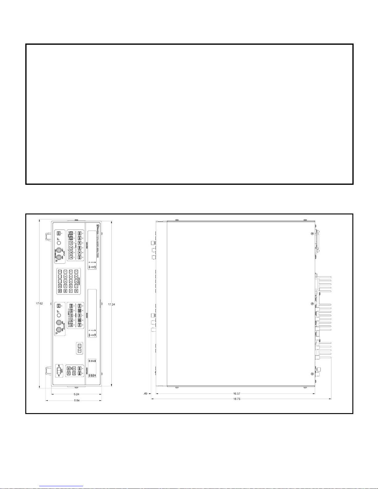
Dimensions:
17.34 inches (44.04 cm) wide, 5.88 inches
(14.9 cm) high, 18 inches (45.8 cm) deep
Weight: 25 lbs (11.3 kg)
Accessories Included:
Spare input, output and line fuses and AC power
cord
Accessories Available:
950044 Rack mounting hardware
950043 Chassis slide kit
954018 Single binding post to BNC (M)
954019 BNC (F) to phono plug
954020 Phono jack to BNC (M)
954021 Two conductor shielded balanced line, 36”
954022 XLR Audio connector to three banana plugs
Function
First Reading
Rate:
Frequency
< 1 sec
4 rdngs/sec
Level
< 1 sec
10 rdngs/sec
Distortion
< 1 sec
8 rdngs/sec
SINAD
< 1 sec
8 rdngs/sec
S/N
< 2 sec
1 rdngs/sec
General Information Section 1
1-5
TABLE 1-1 PERFORMANCE SPECIFICATIONS
Options:
-01 Rear panel input and output
-11 400 Hz high-pass filter
-12 CCITT band-pass filter
-13 CCIR band-pass filter
-15 A weighting filter
-16 B weighting filter
-17 C weighting filter
-18 Audio band-pass filter
-19 C-Message band-pass filter
Remote Interface:
IEEE-488-1978. Implements AH1, SH1, T6, TE0, L4,
LE0, SR1, RL1, PP0, DC1, DT1, C0, and E1
Ventilation Requirements:
1-1/2 inch clearance after installation, top, side,
rear
Temperature:
Non-Operating: -40 to 75 degrees C
AltitudeOperating: 10,000 Ft EEC,
Humidity: and 95% (non-condensing)
Battery Type: Refer to page 6-12
CE MARK: Declares Conformity to European Community
(EC) Council Directives 89/336/EED//93/68/EEC,
73/23/EEC//93/68EEC & Standards EN55011,
EN50082-1
Figure 1-1. Outline Dimensions.

Section 1 General Information
1-6
This page intentionally blank.
Installation Section 2
2-1
SECTION II
INSTALLATION
2-1. INTRODUCTION.
2-2. This section contains the unpacking, mounting,
power requirements, cable connections, and preliminary
check-out instructions for the Model 1121A Audio
Analyzer.
2-3. UNPACKING.
2-4. The instrument is shipped complete and is ready to
use upon receipt. Unpack the instrument from its shipping container and inspect for damage that may have
occurred during shipment. Refer to Figure 2-1.
NOTE
Save the packing material and container for
possible use in reshipment of the instrument.
2-5. MOUNTING.
2-6. For bench mounting choose a clean, sturdy, un-
cluttered mounting surface. For rack mounting, an
accessory kit is available which provides mounting ears.
The rack mounting kit contains the required hardware and
instructions.
2-7. POWER REQUIREMENTS.
2-8. The instrument has a tapped power transformer and
two line voltage selection switches which permit
operation from 100, 120, 220, or 240 volt ± 10%, 50 to
400 Hz, single phase AC power sources.
Always make certain that the line voltage selection
switches are set to the correct positions corresponding to
the voltage of the AC power source, and that a fuse of the
correct rating is installed before connecting the
instrument to any AC power source.
2-9. Set the rear panel line voltage selector switches to
the appropriate positions as indicated in the Line Voltage
Select Chart and check that the line fuse is correct for the
selected power source.
2-10. CABLE CONNECTIONS.
2-11. Front panel connector:
INPUT. Analyzer Input HIGH and LOW BNC type
connectors and chassis ground allow connection of external audio signals for analysis. The input impedance is
100 k ohms either side to ground. The LOW terminal is
connected to chassis ground in the non-floating mode.
OUTPUT. Source output HIGH and LOW BNC type
connectors and chassis ground allow connection to external devices and components. The output impedance is
selected using special functions 75, 76, and 77. The LOW
terminal is connected to chassis grounding the
non-floating mode.
2-12. Rear panel connectors:
MONITOR. The MONITOR BNC type output con-
nector provides a scaled output of the input signal in the
level, frequency and signal-to-noise measurement modes
and a scaled output of the input signal with the
fundamental removed in the distortion and SINAD measurement modes. The output impedance is 600 ohms.
X CLK. The X CLK BNC type input connector provides
a means of connecting to an external 10 MHz counter
reference. The external reference is automatically
selected when a TTL level signal is present.
SYNC. The SYNC BNC type output connector
provides a TTL compatible signal relative to the source
frequency setting.
X AXIS. The X AXIS BNC type output connector
provides a 0 to 5 volt d.c. level relative to the sweep
frequency or level in the sweep mode. The output impedance is 1000 ohms.
Y AXIS. The Y AXIS BNC type output connector
provides a 0 to 5 volt d.c. level relative to the analyzer
measurement and entered HIGH and LOW plot limits.
The output impedance is 1000 ohms.
PEN. The PEN BNC type output connector provides a
TTL compatible signal to control the pen of an external
recorder.
VAC
100
220
50 to
± 10%
120
240
400 Hz
Fuse
3/4 A T
3/8 A T
80 VA
Section 2 Installation
2-2
2-13. PRELIMINARY CHECK.
2-14. The preliminary check verifies that the Model
1121A is operational and should be performed before the instrument is placed into use. To perform the preliminary check,
set the front panel LINE switch to ON. Wait several seconds then depress the LCL/INIT key. The SOURCE display will
contain the instrument firmware number and the other displays will contain dashes for a period of about two seconds. The
SOURCE display will then contain 1000.00 Hz with the KYBD legend illuminated. The ANALYZER display will contain the
message for one level measurement cycle. The initialize sequence resets all functions and operating modes of
the Model 1121A to the initialized values and conditions listed in Table 2-1.
TABLE 2-1. INITIAL CONDITIONS.
Analyzer Group: Source Group: Sweep Group: Bus/Prgm Group:
LEVEL function enabled KYBD legend illuminated SWEEP disabled ADRS is unchanged
Linear display units FREQ function enabled START set to 20.000 Hz PRGM is set to 99
RATIO mode disabled FREQ set to 1000.00 Hz STOP set to 20.000 kHz SRQ is cleared
Filters disabled FREQ STEP set to 0.000 Hz LOW set to 0.000 mV Bus status is unchanged
FLOAT mode disabled LEVEL set to 0.0 mV HIGH set to 300.0 V
RMS detector enabled LEVEL STEP set to 0.0 mV
SPCL functions 0, 10, 40, 55,
63, 70, 77, and 80 are selected
FOAT mode disabled
2-15. Program location 99 is a recall-only location which contains the initialize values. The operating conditions at the time
the instrument power is interrupted are maintained in non-volatile memory and restored when power to the Model 1121A is
resumed.
Installation Section 2
2-3
Figure 2-1. Packing and Unpacking Diagram.

Section 2 Installation
2-4
This page intentionally blank.

Operation Section 3
3-1
SECTION III
OPERATION
3-1. INTRODUCTION.
3-2. This section contains the operating instructions for
the Model 1121A Audio Analyzer.
3-3. OPERATING CONTROLS, INDICATORS AND
CONNECTIONS.
3-4. The controls, indicators and connectors used during
the operation of the instrument are listed in Table 3-1 and
shown in Figures 3-1 and 3-2.
3-5. OPERATING INSTRUCTIONS.
3-6. The operating instructions for the Model 1121A are
divided into sections of Initial Conditions, Local Operation
and Remote Operation.
3-7. INITIAL CONDITIONS.
3-8. Initialize the instrument as follows:
a. Connect the power cord to the instrument and to
the desired power source. Refer to paragraph 2-7 for
proper power application.
b. Set the front panel power switch to ON.
c. Depress the LCL/INIT key.
d. The SOURCE display will contain the instrument
firmware identification number and the other displays will
contain dashes for a period of about two seconds. The
SOURCE display will then contain 1000.00 Hz with the
KYBD legend illuminated and the ANALYZER display
will change to contain the message for one level
measurement cycle.
3-9. LOCAL OPERATION.
3-10. Function Selection. The DATA ENTRY keypad is
common to all functions of the Model 1121A. The KYBD
legend determines the active display window to which the
DATA ENTRY keypad is dedicated at any given time. To
select a function simply depress the function key desired.
The results will be the LED of the function key will be
illuminated, the current value of the selected function will
be displayed in the window above the key, and the KYBD
legend will be illuminated in the display window. The
DATA ENTRY keypad is dedicated to the selected
function and any unit selection or number entry
will appear in the active display window. When selecting
measurement functions the message may appear
to indicate that a measurement cannot be displayed
instantly for any of five possible reasons:
1. The first measurement cycle is in progress and
cannot be displayed.
2. The measurements’ minimum signal require-
ments are not met, for example, frequency measurements cannot be made if the input level is too low.
3. The input level is overrange.
4. The input signal is changing faster than the
analyzer can respond.
5. The notch filter is in the process of being tuned to
the fundament frequency in the distortion or SINAD
modes.
3-11. Data Entry Operation. Once a function has been
selected, new values may be entered with the DATA
ENTRY keypad. To enter data simply depress the
desired digit keys followed by the appropriate unit key or
ENTER key. During digit selection a (‘) mark will
appear in the display to the left of the first digit selected
to indicate the number in the display is in the process of
being entered. No action is taken until the unit or ENTER key is depressed. The unit keys can also be used
aside from number entry to select display modes. For
example, to change the level measurement displayed in
mV to logarithmic units in dBV, simply select the analyzer
LEVEL key and depress the dB key in the DATA ENTRY
keypad. The display program will calculate and display
the logarithmic value. The ENTER key serves a dual
function as a dimensionless unit key for SPCL, ADRS,
and PRGM number entry and also as a default
unit terminator of V, %, and Hz for functions where more
than one unit can be selected.
3-12. Many of the Model 1121A functions have multiple
display and entry modes. Listed in Table 3-2, Function
Display And Data Entry Units, are the display legends
which can be active for each function along with the unit
keys in the DATA ENTRY keypad which select the available display modes. Argument entry ranges for all the
Model 1121A functions are described in Table 3-3, Valid
Function Argument Range. Number entry out of range of
the selected functions will result in an error displayed in
the SOURCE display window. Errors can be cleared by
depressing any key. If at any time prior to entry a wrong
digit is entered, depress the CLR key to clear and restore
the previous display.

Section 3 Operation
3-2
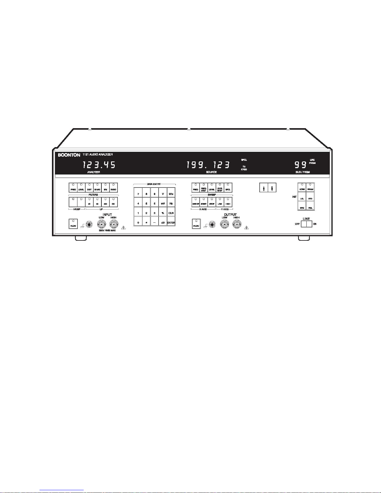
Figure 3-1. Model 1121A, Front View
Figure 3-2. Model 1121A, Rear View
Operation Section 3
3-3
Section 3 Operation
3-4
Operation Section 3
3-5

Section 3 Operation
3-6
3-13. Analyzer Measurement Description. The Model
1121A contains an independent distortion analyzer which
can measure frequency, AC and DC level, distortion,
SINAD and signal-to-noise. In addition, ratio measurements can be made with all analyzer measurement
modes. A wide range of special functions enhance the
basic measurement modes without sacrificing the simplified operation of the analyzer. Standard and optional
audio filters are provided to aid in harmonic distortion
analysis and weighted noise measurements. Finally, the
ability to store and recall specific measurement combinations aid in configuring measurement applications for
manual and remote use.
3-14. Analyzer Input Description. The input configuration of the Model 1121A can be selected for single-ended
or balanced/differential operation. The input mode can
be enabled using the front panel FLOAT key or over the
IEEE-488 bus interface.
3-15. Frequency Measurement Function. The Model
1121A measures wide ranges of audio frequency with
high accuracy and resolution. Microprocessor control of
the reciprocal counter results in automatic selection of
frequency ranges for maximum resolution. Measurements are referenced to an internal 10 MHz timebase
accurate to 0.0001% and external reference capability
is also provided.
3-16. Frequency Measurement Display Units. Frequency measurements can be displayed in Hz or kHz for
values above 199.999 Hz with automatic selection of Hz
units below this limit. To select the Frequency measurement functions simply depress the FREQ key which
illuminates both the key’s LED and the KYBD legend in
the ANALYZER display. Display units can then be
selected by depressing the Hz or kHz keys.
3-17. Special Frequency Measurement Modes.
Special function 11 is provided to preset and hold spe
cific level ranges for frequency measurement. Refer to
paragraph 3-65. The frequency measurement mode can
function to input levels 14 db below the selected level
range. For example by setting the 3.000 volt level range,
measurements can be made with signal levels as low as
600 mV.
3-18. Level Measurement Function. The Model 1121A
measures both AC and DC voltage with high dynamic
range and selectable AC bandwidth. Resolution at full
scale is 3000 counts with an additional 33% overrange
capability. The AC rms detector is true rms responding
for signals with crest factors less than 3. Average and
quasi-peak responding detectors (rms calibrated) can
also be selected. Refer to paragraph 3-74. A period
sampling measurement technique is employed which
results in adaptive measurement rates optimized to the
period of the dominant AC component of the input signal.
This technique yields fast settled measurements in the
AC level mode while effectively filtering large AC components in the DC level mode. Measurement bandwidth
is selectable using the standard and optional filters to
reject out-of-band noise or provide industry-standard
weighting characteristics.
3-19. Level Measurement Display Units. AC and DC
level measurements can be displayed in linear or logarithmic units. Linear measurements are displayed in mV
or V with V automatically selected for levels above 750
mV and mV automatically selected for levels below 0.300
V. Logarithmic measurements are displayed in various
forms. The default mode uses dBV units (dB relative to
1.000 V rms). Power in dBm units (dB relative to 1 mW)
can be selected for various impedances as described in
paragraph 3-74. To select the Level measurement
function simply depress the LEVEL key which illuminates
both the key’s LED and the KYBD legend in the
ANALYZER display. The various display modes can then
be selected by depressing the appropriate units
associated with the desired display mode. For example,
to select AC level in logarithmic units depress the dB key
and to return the display to linear units depress the mV or
V keys.
3-20. Special Level Measurement Modes. Special
function 11 is provided to preset and hold specific level
ranges to achieve faster first measurement rates and to
eliminate possible range-to-range nonlinearity. Refer to
paragraph 3-65. Special function 17 extends the measurements sampling period to provide a more consistent
reading in the presence of noise. AC and DC calibration
is performed through the use of special function codes 20
through 24. The rms, average or quasi-peak AC
detector type can be selected using special function 70,
71 or 72, respectively. Special functions 80 through 86
select logarithmic display modes in dBV or dBm units.
3-21. Distortion Measurement Function. The Model
1121A measures total harmonic distortion and noise over
a
wide range of frequency. The notch filter is automatically
tuned to reject the fundamental frequency and pass only
the harmonic and noise content. The AC measurement
techniques are similar to those used in the level measurement function yielding fast settled measurements.
Measurement bandwidth is selectable to reject noise
while accurately preserving harmonic components.
Measurement results can be displayed in several forms.
The combination of harmonics and noise can be
displayed as an absolute level in mV, V, dBV or dBm units
or as a ratio in % or dB units to the total input signal
consisting of fundamental, harmonics and noise.
3-22. Distortion Measurement Display Units. Distortion measurements can be displayed in linear or
logarithmic units. Linear ratiometric measurements are
Operation Section 3
3-7
displayed in % while logarithmic measurements are
displayed in dB where 0.00 dB is referenced to 100.0%.
Distortion measurements can also be displayed as an
absolute level in units of mV, V, dBV or dBm. The distortion level display mode is useful to measure noise level in
the presence of a holding tone. The holding tone is
removed by the notch filter and the noise level alone is
measured and displayed. In addition the frequency of
the displayed in Hz or kHz units. To select the
distortion measurement function simply depress the DIST
key which illuminates both the key’s LED and the
KYBD legend in the ANALYZER display. The various
display modes can then be selected by depressing the
the appropriate units associated with the desired display
mode. For example, to select distortion level in logarithmic units (dBV or dBm)depress the DIST key followed in
sequence by the mV or V keys and the dB key. The mV or
V keys select the distortion measurement to be displayed
as an absolute level and the dB key converts the results
to logarithmic unit.
Section 3 Operation
3-8
 Loading...