Biostar U8798 Grand Owner's Manual

UU88779988 GGRRAANNDD
FCC Information and Copyright
This equip ment has been tested and fou nd t o com ply w it h the limits of a
Class B digital device, pursuant to Part 15 of the FCC Rules . These limits are
designed to provide reas onable protection against harmful interference in a
residential installation. T his equipment generates , uses and c an radiate
radio frequency energy and, if not install ed and used in ac c ordance wit h the
in structions, may cause harmful interfer ence to radi o communications.
There is no guarantee that interference will not occur in a particular
installa tion.
The vendor makes no representations or warranties with respec t to the
con tents here a nd special ly disclaims any implied warranties of
merchantability or fitness fo r any purpos e. F urther the vendor rese rves the
right to revis e this publication and to make changes to the contents here
w ithout obligat ion to notify any party beforehand.
Duplication of this public ation, in part or in whole, is not allowed without first
obt ainin g the vendor’s approval in writi ng.
The con te nt of thi s u ser’s m anu al is subje ct to be chan ge d with ou t noti ce
and we will not be responsible for any mistakes found in this user’s manual.
All the br and an d product name s are trad emark s of their re spe ctive
companies.
1

UU88779988 GGRRAANNDD
TABLE OF CONTENTS
Chapter 1: Introduction.......................................3
1.1 U8798 GRAND Features......................................3
1.2 Package Checklist..................................................5
1.3 Layout of U8798 GRAND....................................6
1.4 Components of U8798 GRAND...........................7
Chapter 2: Hardware Installation........................8
2.1 Central Processing Unit (CPU) .............................8
2.2 Memory Modules..................................................9
2.3 Jumpers, Headers, Connectors, & Slots................9
2.4 Award BIOS beep code.......................................14
2.5 Troubleshooting...................................................15
Chapter 3: WarpS peeder™............................16
3.1 Introduction.........................................................16
3.2 System Requirement............................................16
3.3 Installation...........................................................16
2
UU88779988 GGRRAANNDD
CHAPTER 1: INTRODUCTION
1.1 U8798 GRAND FEATURES
A. Hardware
CPU
Supports Socket 478.
Supports Intel Pentium 4 Processor.
Supports Intel Pentium 478-pin Prescott CPU.
- 533FSB with 1024KB L2 Cache
- Celeron D (533 FSB with 256KB L2 Cache)
- 800 FSB with 1024KB L2 Cache up to 3.2GHz.
Supports Intel Hyper-T hreading Technology.
Front Side Bus at 400/533MHz.
Front Side Bus 800MHz is by overclocking
Chi pset
North Bridge: P4X533CD
South Bridge: VT8235CE
Ma in Memory
Supp orts up to 2 DDR devices.
Supp orts 266/ 333M Hz DDR devi ces.
400MHz DDR is suppor ted by ov er cl oc king.
Maximum me mo r y s iz e is 2GB.
Super I/O
Chip: ITE IT8 705AF.
Provides the most commonly used legacy Super I/O
functionality.
Environment Control initiatives,
- H/W Monitor
- Fan Speed Controller (optional)
- IT E's " S mart Guardi an" functio n
Meet th e “Mi cro soft PC98 & PC99 Syste m Desi gn Guide”
requirements.
Slots
5 32-bit PCI bus master slots.
1 AGP 4x / 8x co m patib l e s lot.
1 CNR sl ot (optional).
On Board IDE
Supports 4 IDE disk drives.
Supports PIO m ode 0~4, Block Mode and Ultra DMA
33/ 66/10 0/133 bus mas t er mo de.
LAN PHY
PH Y: VIA VT6103L
Supports 10 Mb/s and 100 Mb/s auto-negotiation.
3
UU88779988 GGRRAANNDD
Half/Ful l duplex ca pabil ity.
Sup por ts ACPI/ PC I pow er ma na ge me nt
On Board AC’97 Sound Codec
Chip: C-Media CMI9761A
Compliant with AC’97 speci fication.
Sup por ts SPD IF out function (opti ona l).
Supports 6 channels.
Supports stereo mi crophone.
Serial A TA ( With SB VT8237CD only)
Integrated in South Bridge VT8237
Supports RAID 0, RAID 1.
Supports 2 serial ATA (SATA) ports,
- Compliant with SATA 1.0 spec.
- Data transfer rate up to 150 MB/s.
On Board Peripherals
a. Rear side
1 par all el port.
1 audio ports in vertical.
1 RJ - 45 LAN jack.
1 PS/2 keyboard and 1 PS/2 mouse port.
1 serial port (COM2 is optional).
2 USB 2.0 ports.
4 USB 2.0 ports are supported by SB VT8237CD.
b. Front S i de
1 fl oppy port supports 2 FDDs with 360K, 720K, 1.2M ,
1.4 4M an d 2.88M byt es .
1 S/PD IF out header ( optional)
1 Front audio header
1 Front panel header.
4 USB2.0 ports.
Dimensions
AT X Form Fa ctor: 1 9.9 x 29.3 cm (W x L)
B. BIOS & Software
BIOS
Award legal BIOS.
Supports APM1.2.
Supports ACPI.
Supports USB Function.
Software
Sup por ts W ar pspee der ™, 9th T o uc h™, W IN FLA SH ER™
and FLASHER™.
Offers the hi ghest performance fo r Win dows 98 SE,
Windows 2000, Windows M e, Windows XP, SCO UNIX etc.
4

UU88779988 GGRRAANNDD
1.2 PACKAGE CHECKLIST
FDD Cable x 1
HDD Cable x 1
User’s Manual x 1
Fu lly Setup Drive r CD x 1
USB 2.0 Cable x1 (optional )
Serial ATA Cable x 2 (opti onal)
S/PDIF Out Cable x 1 (optional)
Rear I/O Panel for ATX Case x 1
5
UU88779988 GGRRAANNDD
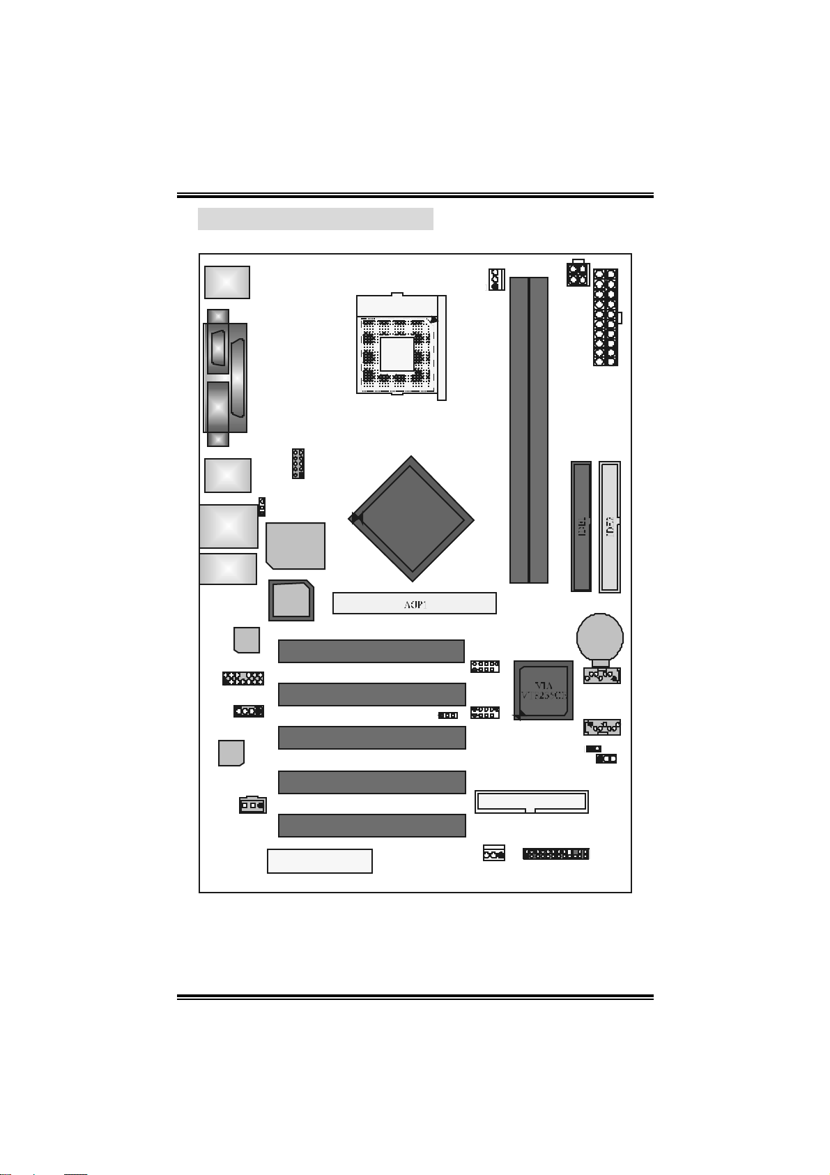
1.3 LAYOUT OF U8798 GRAND
JKB MS1
JC O M1
JPRNT1
COM 1
Parallel Port
Socket 478
PU
CPU1
JCFAN1
JATXPWR2
JATXPWR1
JUSB 1
JUSB LAN1
JAUDI O
LAN
PHY
JAUDIO1
2
1
JC DIN1
CODEC
JSPDI FO1
JCOM2-HEADER
10
2
JUSBV1
1
ITE I/O
BIO S
14
13
1
1
CNR1 (op tional)
DIMM1
9
1
DIMM2
P4X
533CD
PCI1
PCI2
PCI3
PCI4
PCI5
1
JUSBV2
JU SB 3
1 9
JU SB 4
1 9
JSFAN1
102
102
FDD1
2
1
1
JPANEL 1
BAT1
714
JSATA2
JSATA1
17
4
JCI1
1
JC M OS1
24
23
Note: ● represents the 1st pin.
6
UU88779988 GGRRAANNDD
L
O
P
T
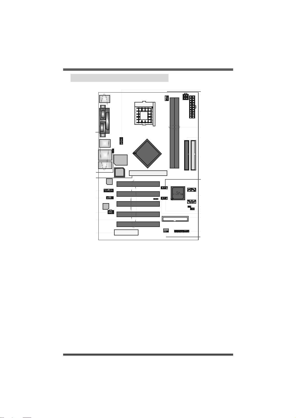
1.4 COMPONENTS OF U8798 GRAND
PU
S ocket 478
A
P4X
ITE I/O
53 3CD
X
W
V
U
S
R
CO DEC
BIO S
LAN
PHY
B
C
D
E
F
G
H
Back Panel Connec t ors
A.
JU SBV1: Power Source Selection f or
B.
JU SB1 & PS/2 k eyboard/mouse.
Acc elerat ed Graphics Port Slot
C.
(AGP1)
Front Panel Audio Header
D.
(JAUDIO1)
CD -ROM Audio-In H eader (JCDIN 1)
E.
Digit al Audio Connector (JSPDIFO1)
F
(optional)
Peripheral Com ponent I nt erconnect
G.
Slots (PCI 1-5)
Communication Network Riser Slot
H.
(CNR1) (opt ional)
Syste m Fan Header ( JS FAN1)
I.
Front Panel Connec t or (JPAN EL1)
J.
Floppy Disk Connector ( FDD1)
K.
USB C onnector Power Sourc e
L.
(JUSBV2)
Q
N
M
K
J
I
Front USB Header ( JUSB4)
M.
Clear CMOS Jumper (JCMOS1)
N.
Cas e Open Connec t or (JCI 1)
O.
Serial ATA Connectors (J SATA1-2) (f or
P.
SB VT8237CD only)
Front USB Header ( JUSB3)
Q.
Hard D isk Connec t ors (ID E1-2)
R.
DDR DIMM Modules (DIMM1-2)
S.
AT X Power Connec t or (JATXPWR 1)
T.
AT X Power Connec t or (JATXPWR 2)
U.
CPU Fan Header ( JCFA N1)
V.
JC OM2-Header: COM2 H eader
W.
(optional).
7
UU88779988 GGRRAANNDD
CHAPTER 2: HARDWARE INSTALLATION
2.1 CENTRAL PROCESSING UNIT (CPU)
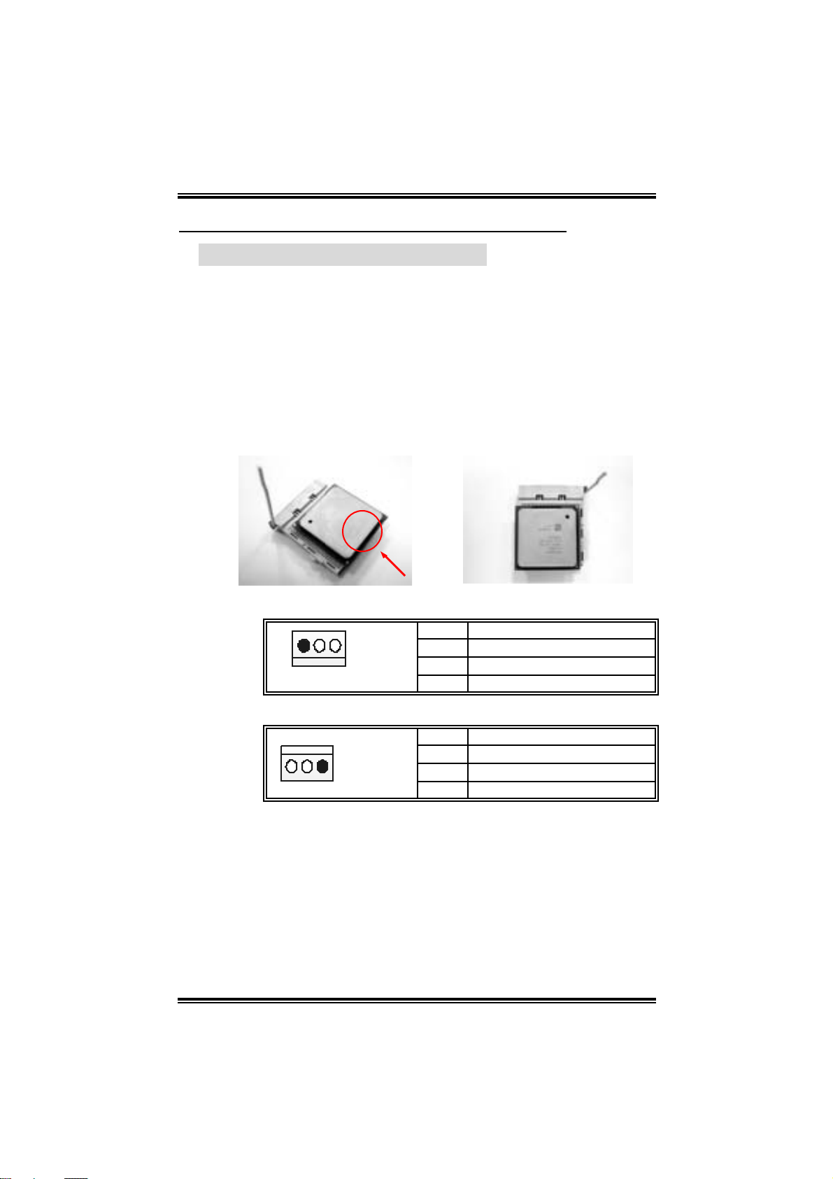
Step 1: Pull the lever sideways away from the socket and then raise
the lever up to a 90-degree angle.
Step 2: Look for the white dot/cut edge. The white dot/cut edge should
point wa rds th e lever pi vot. The CPU will fit onl y in the corre c t
orientation.
Step 3: Hold the CPU down fi rmly, and then cl ose the lever to com plete
the i nstal la ti on.
Step 4: Put the CPU F an on t he CP U and buckl e it . Co nn ec t the CP U
FAN power cable to the JCFAN1. This completes the
installation.
CPU FAN He ader: JC FAN1
Pin Assignment
1
JCFAN1
1 Ground
2 +12V
3 FAN RPM rat e sense
System Fan Header: JSFAN1
Pin Assignment
1 Ground
1
JSFAN1
Note:
The JCFAN1 and JSFAN1support system-cooling fan with
+12V. It supports 3-pin head connector. When connecting with
wires onto connectors, please note that the red wire i s the
positive and should be connected to +12V, and the black wire
is Ground and should be connected to GND.
2 +12V
3 FAN RPM rat e sense
8
UU88779988 GGRRAANNDD
2.2 MEMORY MODULES
Supp orts up to 2 DDR devices.
Supp orts 200/ 266/333 MHz DDR devi c es.
Maximum memory size i s up to 2 GB.
DI MM Socket
Location
DIMM1 128MB/256MB/512MB/1GB *1
DIMM2 128MB/256MB/512MB/1GB *1
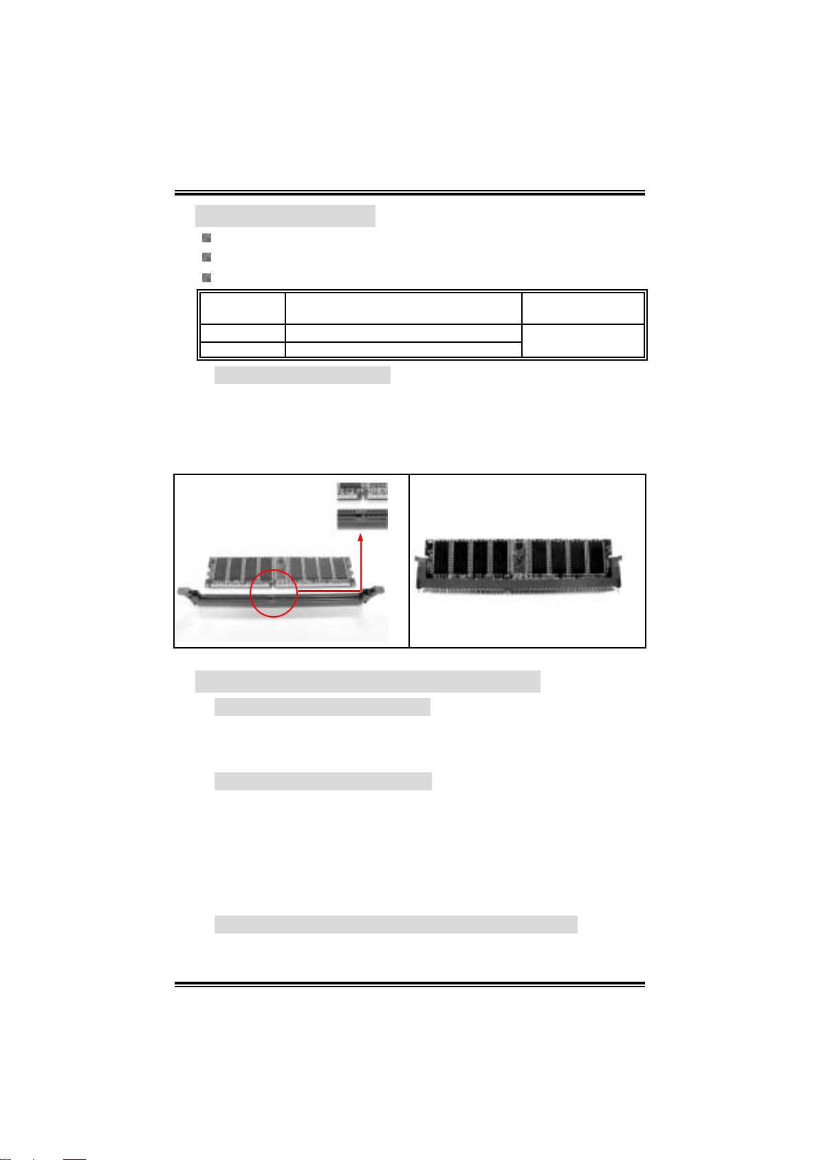
DDR Module
DDR Modu le ins tallation
1. Unlock a DIMM slot by pressing the retaining clips outward. Align a
DIMM on the slot such that the notch on the DIMM matches the
break on the Slot.
2. Insert the DIMM vertically and firmly into the slot until the retaining
chip snap back in place and the DIM M is properly seated.
Total Memor y Size
Max is 2 GB.
(MB)
2.3 JUMPERS, HEADERS, CONNECTOR S, & SLOTS
Floppy Disk Connector: FDD1
The motherboard provi des a standard floppy disk connector that
s uppor t s 360K , 720 K, 1.2 M, 1.44 M and 2. 8 8 M f lo ppy d is k types. Th is
connector supports the provided floppy drive ribbon cables.
Hard Disk Connectors: IDE1~2
The motherboard has a 32-bit Enhanced PCI IDE Controller that
provides PIO Mode 0~5, Bus Master, and Ul tra DMA 33/ 66/ 100
functio nalit y. It ha s two HDD c onne c to rs IDE1 (primary) an d IDE2
(secondary).
The IDE connectors can connect a master and a slave drive, so you
can connect up to four hard disk drives. The first hard drive should
al ways be con nected to IDE1.
Peripheral Component Interconnect Slots: PCI 1~5
This motherboard is equipped wi th 5 standard PCI sl ots. PCI stands for
Peripheral Component Interconnect, and it i s a bus standard for
9

UU88779988 GGRRAANNDD
expansi on cards. T his PCI slot is designated as 32 bits.
Accelerated G raphics Port Slot: A GP1
You r mon itor will atta c h dire c tly to that vide o card. Thi s motherbo ard
supports video cards for PCI slots, but it is also equipped with an
Accelerated Graphics Port (AGP). An AGP card will take advantage of
AGP technology for improved video efficiency and performance,
especially with 3D graphics.
Commun icati on Netw ork R iser Slot: CNR1 (Optional)
The CNR specification is an open In du stry Standard Archi tec ture, an d it
defi nes a hardware scalable riser card i nterface, which supports
modem onl y.
Serial ATA Connector: JSATA1~2 (With SB VT8237CD only)
The motherboard has a PCI to SATA Controller with 2 channels SATA
interface, i t satisfies the SATA 1.0 spec and with transfer rate of
1.5Gb/s.
Power Sourc e Se lect io n for JUSB1, P S/2 Keyb oa r d/ M ou s e :
JUSB V1
JUSBV1 Assignment Description
13
Pin 1-2 close
Pin 2-3 close
13
+5V
+5V Standby
Voltage
+5V for JUSB1 and PS /2
keyboard / mouse.
JU SB1 and PS/2
key board/mous e are
powered wit h +5V
standb y voltage.
Note:
In order to support this function “Power-on system via
keyboard and mouse”, “JUSBV1” jumper cap should be placed
on Pin 2-3.
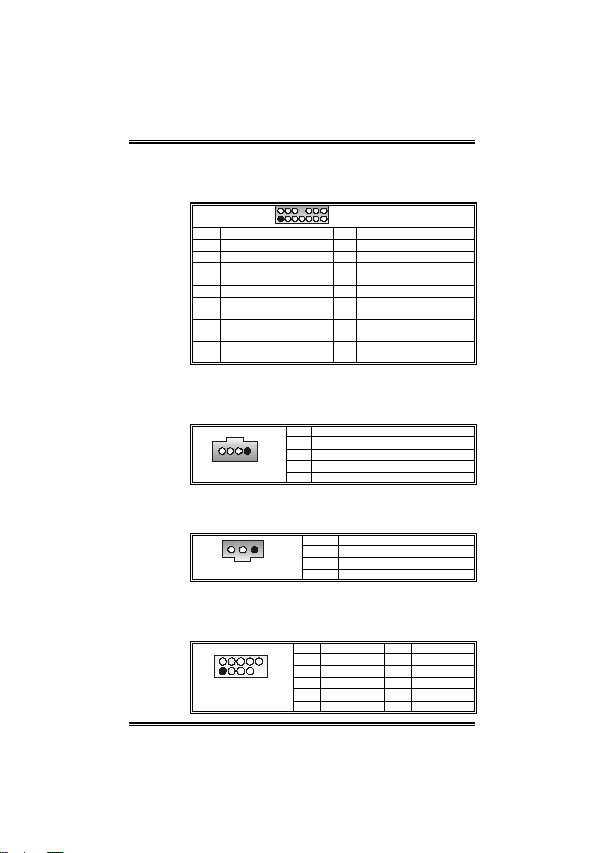
COM2 Header: JCOM2-Header (Optional)
This header allows user to connect additional serial cable on the
PC back panel. It can be used to connect serial devi ces, for
example, mouse or modem.
910
1
2
Pin Assignment Pin Assignment
RIN1
1
DOUT2
3
Ground
5
DOUT1
7
-XRI1
9
JCOM2-Header
2
4
6
8
10
10
RIN3
DOUT3
RIN2
RIN4
NA
UU88779988 GGRRAANNDD
Front Panel Audio Out Header: JAUDIO1
This connector allows user to connect with the front audio out put
headers on th e P C front panel. It will disable the out pu t on ba c k
panel audio connector s.
2
1
Pin Assignment Pin Assignment
1 Mic in/center 2 Ground
3 Mic power/Bas s 4 Audio power
Right line out/ Speaker
5
out R ight
7 Reserved 8 Key
Lef t line out/Speaker out
9
Lef t
Right line in/R ear
11
speaker Right
Lef t line in/R ear speak er
13
Lef t
14
13
JAUDIO1
Right line out/ Speaker out
6
Right
Lef t line out/Speaker out
10
Lef t
Right line in/R ear speaker
12
Right
Lef t line in/R ear speak er
14
Lef t
CD- ROM A udio- in H e ader: J CDI N 1
This connector allows user to connect the audio source from the
ve riaty de v ice s, like CD-RO M, DVD-ROM, PCI sound c ard , PCI TV
turner card etc..
Pin Assignment
1 Lef t channel input
1
JCDIN1
2 Ground
3 Ground
4 Right channel input
Digital Audio Out Connector: JSPDIFO1 (Optional)
This connector allows user to connect the PCI bracket SPDIF
out put head er .
Pin Assignment
1 +5V
2 SPDIF OUT
3 Ground
JSPDIFO1
1
Front USB Heade r: JUSB3~4
This connector allows user to connect additional USB cables on the
PC front panel. Also can be connected wi th internal USB devices,
like U SB c ard reader.
Pin Assignment Pin Assignment
2
1
10
9
JUSB3/4
1 +5V (fused) 2 +5V (f used)
3 USB- 4 USB5 USB+ 6 USB+
7 Ground 8 Ground
9 Key 10 NC
11
UU88779988 GGRRAANNDD
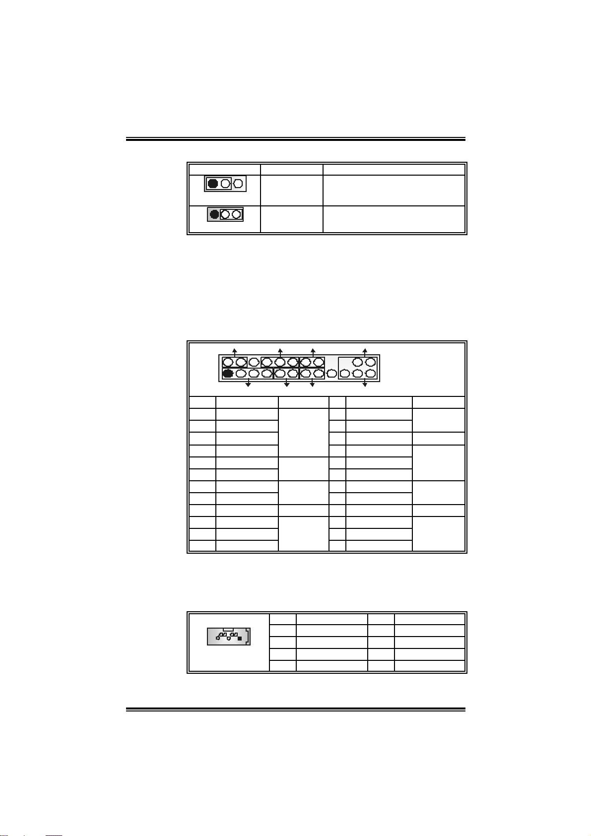
Power Source Select ion for USB: JUSBV2
JUSBV2 Assignment Description
1 3
Pin 1-2 close
1 3
Pin 2-3 close
+5V
+5V st andby
Voltage
+5V for USB loc at ed at t he
JU SB3~4 port connectors
JU SB3~4 port s are powered with
st andby v olt age of +5V
Note:
In order to support this function “Power-o system via USB
dev ic e,” “J U SB V 2” jump er ca p s hould be placed on P in 2- 3
individually.
F r ont Pa n el Conn ector: JPA N EL1
This 24-pin c on ne c tor incl ud es Powe r-on, Reset , HDD L ED, Po wer
LED, Sleep button, speaker and IrDA Connection. It allows user to
connect the PC case’s front panel switch functions.
SPK
PWR_LED
HLED
Speaker
Connector
Hard driv e
LED
Reset
button
IrDA
Connector
RST
8 Power LED (+)
12 Power LED (-)
16 Ground
24 IRRX
IRON/OFF
24
IR
JPANEL1
Sleep butt on
Power LED
Power-on
button
IrDA
Connector
SLP
2
123
Pin Assignment Function Pin Assignment Function
1 +5V 2 Sleep control
3 N/A 4 Ground
5 N/A 6 N/A N/A
7 Speaker
9 HDD LED (+) 10 Power LED (+)
11 HEE LED (-)
13 Ground 14 Power button
15 Reset control
17 N/A 18 Key
19 N/A 20 Key
21 +5V 22 Ground
23 IRTX
Se rial ATA co nnector JSATA1~ 2 (With SB VT82 37CD only)
The motherboard has a PCI to SATA Controller with 2 channels
SAT A in te rface , it sa tisfies the SATA 1.0 sp e c and wi th tra n sfer rate
of 1.5Gb/s.
Pin Assignment Pin Assignment
1 Ground 2 TX+
JSATA1/JSATA2
1234567
3 TX- 4 Ground
5 RX- 6 RX+
7 Ground
12
UU88779988 GGRRAANNDD
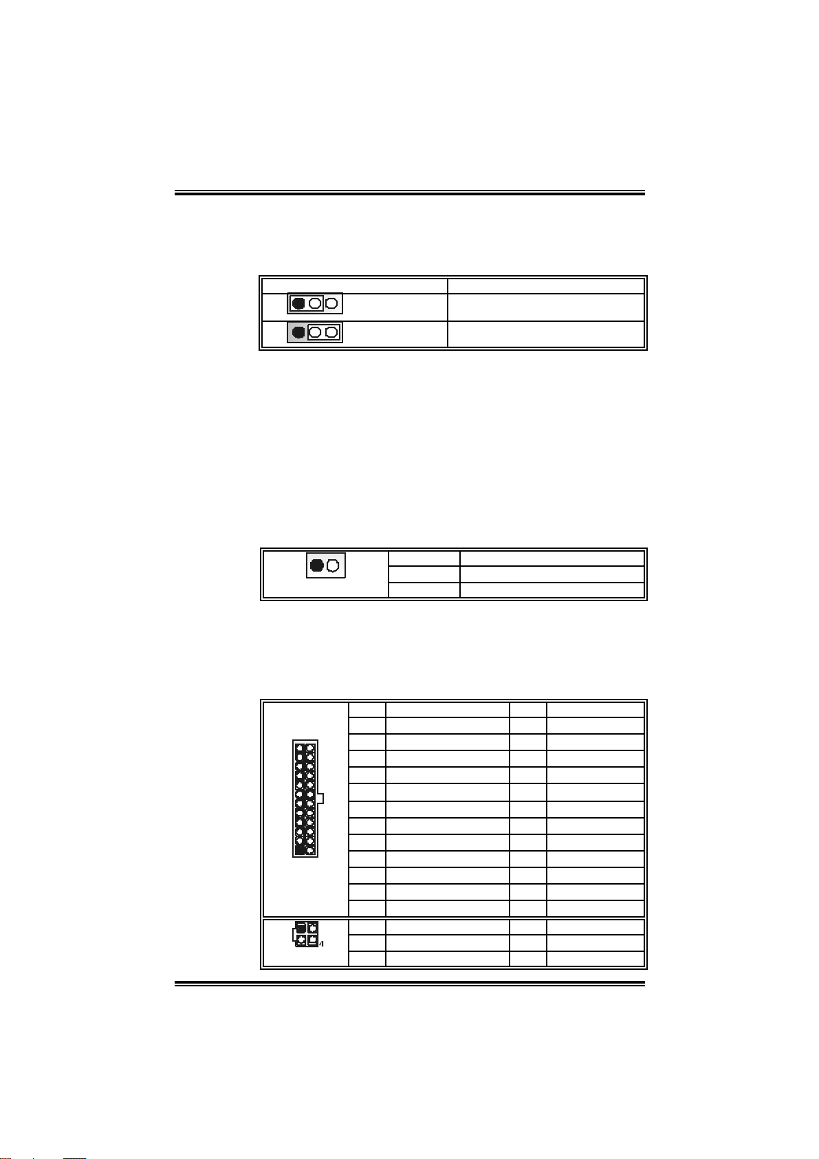
Clear CM OS Jump er: JCM OS1
By placing the jumper on pin2-3, it allows user to restore the BIOS
safe setting and the CMOS data, please carefully follow the
pr oced ur es to avo id da ma g ing th e mot her boar d .
JCMOS1 Assignment
1 3
1 3
Pin 1-2 close
Pin 2-3 close
Norm al Operation (D ef ault).
Clear CMOS data.
※ Clear CMOS Procedures:
1. Remov e AC power line.
2. Set the jumper to “Pin 2-3 cl ose”.
3. Wait for fi ve seconds.
4. Set the jumper to “Pin 1-2 cl ose”.
5. Power on the AC.
6. Reset your desi red password or clear the CMOS data.
Case Op en Connector: JCI1
T his connecto r allows syste m to mo nitor PC case open status. If
the s i gnal has be en tr i ggered, it will record to t he CMOS and show
the mes sage on nex t bo ot -up.
12
JCI1
Pin Assignment
1 Cas e open signal
2 Ground
Pow er Conn ector s: JATX PWR1/PAT X PWR2
JATXPWR1: This connector allows user to connect with 20-pin
power co nn ec tor on the A TX pow er s upp ly.
JATXPWR2: By connecting this connector, it will pro vi de + 12 V to
CPU power circuit.
Pin Assignment Pin Assignment
1 +3.3V 13 +3.3V
12
JATXPWR1
JATXPWR2
1
123
24
13
2 +3.3V 14 -12V
3 Ground 15 Ground
4 +5V 16 PS_ON
5 Ground 17 Ground
6 +5V 18 Ground
7 Ground 19 Ground
8 PW_OK 20 -5V
9 Standby Voltage +5V 21 +5V
10 +12V 22 +5V
11 +12V 23 +5V
12 2 x 12 Detect 24 Ground
Pin Assignment Pin Assignment
1 +12V 3 Ground
2 +12v 4 Ground
13
UU88779988 GGRRAANNDD
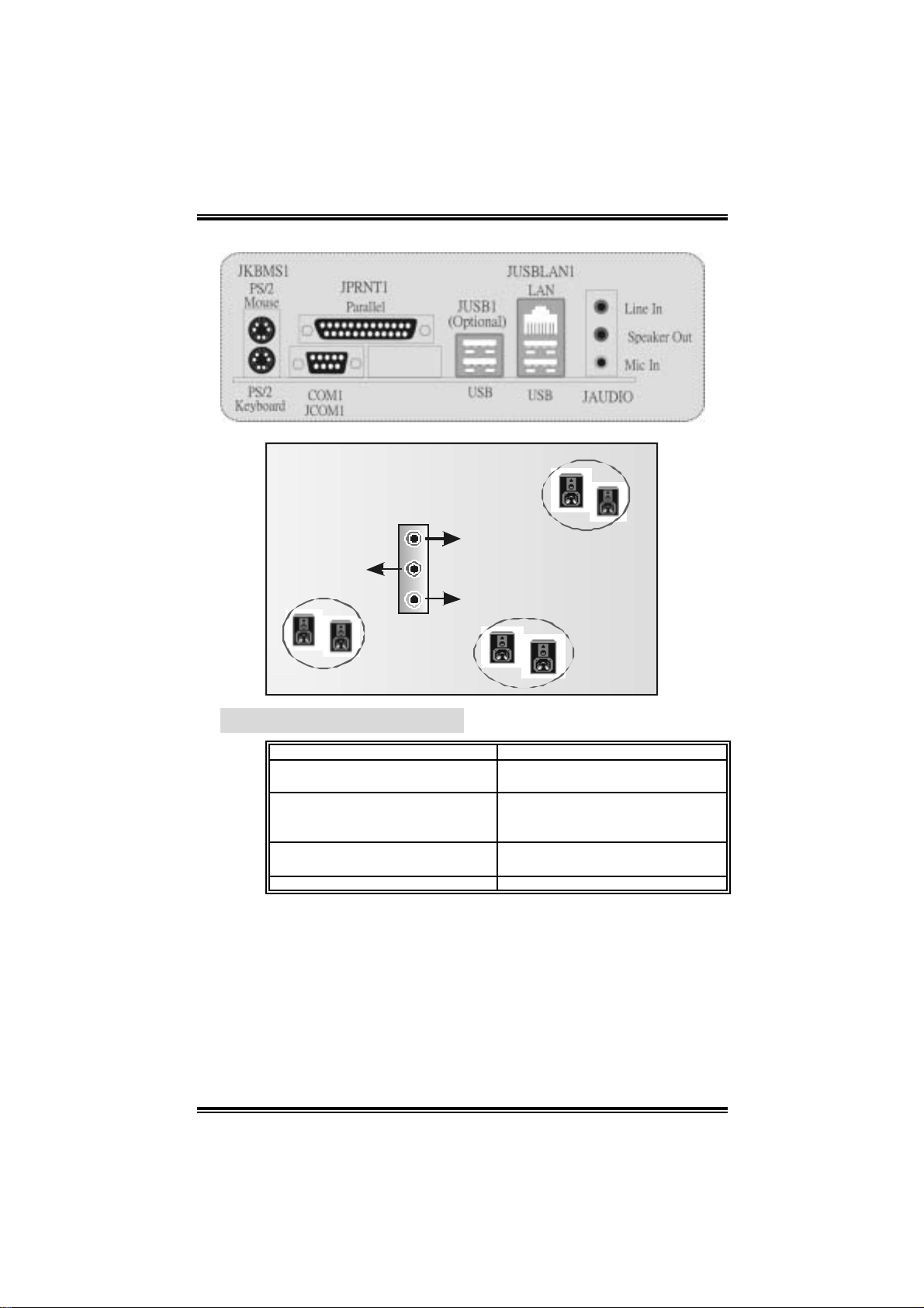
Bac k Panel Connectors
6 Ch anne l Spea k er s
Sp eaker O ut/
Front Speakers
2.4 AWARD BIOS B EEP CODE
One long beep f ollowed by two short
beeps
High-low siren sound 1. CPU overheated
One Short beep when system
boot-up
Long beeps every other s ec ond No DRAM detected or install
Beep Sound Meanin g
Lin e In/
Rear Sp eaker (L eft & R ight)
Mi c In/ C enter & Bass
Video card not f ound or v ideo card
mem ory bad
2. Sys t em will s hut down
automatically
No error found during POST
14

UU88779988 GGRRAANNDD
t
2.5 TROUBL ESHOOTING
Probable Solution
1. No power to the system at all
Power light don’t illuminat e, fan
inside power supply does not
turn on.
2. Indic at or light on k ey board does
not t urn on.
Sys t em inoperat iv e. Keyboard lights
are on, power indic at or light s are lit ,
and hard driv e is spinning.
Sys t em does not boot from hard disk
drive, can be booted from optical
drive.
Sys t em only boots from optical driv e.
Hard disk can be read and
applicat ions can be used but booting
from hard disk is impossible.
Screen m essage say s “Invalid
Conf igurat ion” or “CMOS Failure.”
Cannot boot sys t em after ins t alling
sec ond hard drive.
1. Make sure power cable is
sec urely plugged in.
2. Replace cable.
3. Cont act technic al support.
Us ing even pressure on bot h ends of
the DIMM, press down firm ly until
the m odule snaps into place.
1. Chec k cable running f rom disk
to disk controller board. Make
sure bot h ends are securely
plugged in; check the dri ve type
in the standard CMOS se tup.
2. Back ing up the hard driv e is
ext rem ely im portant. All hard
disk s are c apable of break ing
down at any t ime.
1. Back up dat a and applications
files.
2. Ref orm at the hard drive.
Re-install applications and dat a
using backup disks.
Rev iew system’s equipm ent. Make
sure c orrect informat ion is in setup.
1. Set m aster/slave jumpers
correctly.
2. Run SETUP program and s elec
correc t driv e types. Call t he
drive m anufacturers for
com patibility with ot her drives .
15

UU88779988 GGRRAANNDD
CHAPTER 3: WARPSPEEDER™
3.1 INTRO DUCTION
[WarpSpeeder™], a new powerful control utility, features three
user-friendly functions including Overclock M anager, Overvoltage
Manager, and Hardware Monitor.
With the Overclock Manager, users can easi l y adjust the frequency they
prefer or they can get the best CPU performance with just one click. T he
Overvol tage Manager, on the other hand, helps to power up CPU core
voltage and Memory voltage. The cool Hardware Monitor sm artly
indicates the temperatures, vol tage and CPU fan speed as well as the
chipset information. Al so, in the About panel, you can get detail
descriptions about BIOS m odel and chipsets. In addition, the frequency
status of CPU, memory, AGP and PCI along with the CPU speed are
synchronically shown on our main panel.
Moreover, to protect users' computer systems i f the setting is not
appropriate when testi ng and results i n system fail or hang,
[WarpSpeeder™] technology assures the sy stem stability by
automatically rebooting the computer and then restart to a speed that is
either the origi nal system speed or a suitable one.
3.2 SYSTEM REQUIREMENT
OS Support: Windows 98 SE, Windows M e, Windows 2000, Windows XP
DirectX: DirectX 8.1 or above. (The Windows XP operati ng system
incl udes DirectX 8.1. If you use Windows XP, you do not need to instal l
Dir ec tX 8.1.)
3.3 INSTALL ATION
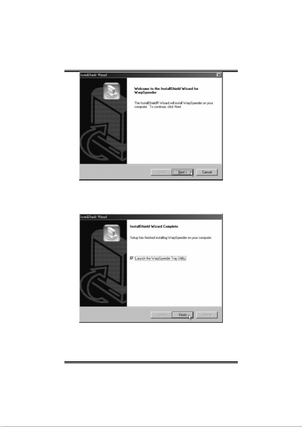
1. Exec ute the setup execut ion file, a nd t he n t he fo llowing dial og will
pop up. Please click “Next” button and follow the default procedure
to ins ta ll.
16
UU88779988 GGRRAANNDD
2. When you see the foll owi ng dialog in setup procedure, it m eans
setup is completed. If the “Launch the WarpSpeeder Tray Utility”
checkbox i s checked, the Tray Icon utility and [WarpSpeeder™]
utility will be automatically and im mediately l aunched after you
click “Finish” button.
Usage:
The following figures are just only for reference, the screen printed in this
user manual will change according to your motherboard on hand.
17
 Loading...