Biostar U8798 Owner's Manual

FCC Infor matio n and Copyright
This equipment has been tested and fo und to c omply with the
limits of a Class B digital device, pursuant to Part 15 of the FCC
Rules. These limits are designed to provide reasonable protection
against harmful interference in a residential installation. This
equipme nt gene rates, uses and can radiate radio frequency
energy and, if not installed and used in accordance with the
instructions, may cause harmful interference to radio
communications . There is no guarantee that interference will not
occur in a particu lar installa tion.
T he vendo r mak es n o rep resent at io ns or wa rran ti es wit h respec t
to the contents here of and specially disclaims any implied
warranties o f me rc ha nt ab il ity o r fi tn es s fo r any purpos e . F urt her
the vendor reserves the right to revise this publication and to
mak e changes to the contents here of without obligation to notify
any party beforehand.
Dup lic ati o n o f t his pu bl ic at ion, i n p a rt o r i n whol e, is n ot al lo wed
w ith out first obtaining the vendor ’s approval in writing.
The content of thi s user’s manual is subject to be cha nged without
notice and we will not be responsible for any mistakes found in
this user’s manual. A ll the brand and product names are
tra demar ks of th eir r e s pe ct ive comp anies.

Table of Contents
Notice..............................................................................................1
Mainboard Features ...............................................................2
1. F e at ures Introduct ion.............................................................2
1-1. Hardware...........................................................................2
1-2. BIO S & Soft wa re ................................................................5
1-3. Pa ckage Contents...............................................................5
2. Mainboard Configur ation ........................................................6
2-1. Layo ut o f U 8798.................................................................6
2-2. Co mpone nt Index...............................................................7
3. CPU Configur ation...................................................................8
3-1. CP U S ocket 478 C onfi guration Steps:.................................8
3-2. CP U F an Header: JCFAN1.................................................10
3-3. System Fan H eader: JSFAN1............................................ 10
4. J umpers, Headers & Connectors.......................................... 11
4-1. Front Panel C onne ctor : JPANEL 1...................................... 12
4-2. AT X 20- pin Power Connector : JATXPWR1......................... 14
4-3. AT X 12V P ower C onnec tor: JATXPWR2............................ 14
4-4. Hard Disk Connector s: ID E1/IDE 2....................................15
4-5. Floppy Dis k C onnect or: F DD 1...........................................15
4-6. W ake On L AN Hea der : JW OL1.......................................... 15
4-7. Cl e ar CMOS Jump er : JCMOS 1.......................................... 16
4-8. Front USB Heade r: JUSB 3................................................16
4-9. Front USB Heade r: JUSB 2................................................17
i

Table of Contents
4-10. 5V / 5VSB Selection for U S B: JUSBV 1.............................17
4-11. 5V / 5VSB Selection for KB : JKB V1.................................. 17
5. RAM Module Configuration ...................................................18
5-1 DD R SD RAM...................................................................... 18
5-2. DI MM Mod ul e C onfiguration............................................. 19
6. Perip her al Port Feat u r es.......................................................20
6-1. PS /2 Mouse / Keyboar d C onnect or : JKBMS1.................... 20
6-2. US B Connect ors: JUSB1................................................... 21
6- 3 . S eri al and Par alle l Int erface Por ts..................................... 22
6-4. Gam e (Joystic k/ MIDI) Por t Conn ec tor: J G A ME1.............. 24
6-5. Audio Por t Conne ctor s: JSPKR1/J LIN 1/JMIC1...................24
6-6. Audio Subsystem ............................................................. 25
ii

Mainboard Features
Notice
I n troduc ti on of s yste m
T hi s ma inboar d is de sign e d to t ak e ad van t ag e of t he la te st indu s try
technology to provide you with the ultimate solution in data
processing. In the tradition of its predecessors, this mainboard
continues a com mitment to reliabil ity and per formance and strives
for full compliance and compatibility with industry s oftware and
ha rdware standards.
U8798 Featur es:
1.Contains on board I/O facilities that include two serial ports, a parallel
port, a PS/2 mouse port, a PS/2 keyboard port, audio ports, USB
ports and a game port.
2.Contains on board IDE facilities for IDE devices such as hard disks
and CD-ROM Drives.
3.Supports the Intel Penti um ® 4 pr o c ess or , a l ead i ng edge proc ess or.
Com pli es with PC ATX form factor specifications.
4.Supports popular operating systems such as Windows NT, Wi ndows
20 00, Windo ws ME, Windo ws X P, No vell, LINUX and SCO UNIX.
1

Mainboard Features
Mainboard Features
1 . Features Introduction
1-1. H ar dwar e
CPU:
1.Provides Sock et -478.
2.Supports the I nt el Pentium ® 4 processor providing t he new generat ion pow er
for high-end w orkstations and s erv ers .
Speed:
1.Runing at 400/ 533 M Hz Front Side Bus f requency.
2.Supports up t o 2.53 GHz CPU core speeds.
3.The 33M Hz 32 bit PCI 2.2 c ompliant.
4.The 66M Hz AGP 2. 0 compliant int erf ace support s 1x, 2x and 4x dat a t rans f er
mode (only with 1.5V).
Chipset:
1.Chipset – VI A VT8754 (P4X400)/ VT8235.
2.I/O Chip – ITE IT8705.
DRAM Memory:
1.Supports 200M Hz, 266M Hz, 333M Hz and 400M Hz DDR devic es.
2.Supports 64M b, 128Mb, 256M b, 512Mb and 1G technologies f or x 8 and 16
devices.
3.Max of 2 Double-Sided DDR w it h unbuffered / Regist ered (with ECC).
4.The largest me mory capac ity is 3 GB.
2

Mainboard Features
Shadow RAM:
Motherboard is equipped with a memory c ont roller providing s hadow RAM and
suppo r t fo r ROM BIOS.
Green Functionality:
1.Supports Award BIOS ™ pow er management f unctionality.
2.Has a power dow n timer f rom 1 t o 15 minut es .
3.Wak es f rom pow er saving sleep mode w it h any k ey board or mous e ac tivity .
BUS Slots:
1.Cont ains 1 AGP slot.
2.Cont a i n s 1 CNR s l ot .
3.Cont ains 5 32-bit PCI bus slots
Flash Mem or y:
1.Supports flas h me mory f unctionality.
2.Supports ESCD functionality.
Built in IDE Facilitie s :
1.Supports four I DE hard disk drives.
2.Supports PI O M ode 4, Master M ode, and high perf ormanc e hard disk drives.
3.Supports disk t ransfer rates up to 133 M B/second.
4.Supports Ultra DMA 33, U ltra DMA 66, Ult ra DMA 100, Ult ra DM A 133 Bus
Master Modes.
5.Supports IDE int erface with CD-ROM.
6.Supports high c apacity hard dis k drives.
7.Supports LBA mode.
3

Mainboard Features
A C’97 Sound Code c O nboard :
1.AC-LINK prot oc ol compliance.
2 . Comp liant wi th A C ’ 97 2. 2 spec i f icat i on.
3.18-bi t full duple x st ereo ADC, DAC s.
4.SNR>95 Bb t hroughmixer and DAC.
5.AC-3 playback required for PVD applications.
I/O facilities :
1.One multi-mode Parallel Port capable of supporting the following
specifications:
St andard & Bidirection Parallel Port.
Enhanc ed Parallel Port (EPP).
Ex tended Capabilit ies Port (ECP).
Nor mal
2.Supports tw o serial ports, 16550 U ART.
3.Supports Inf rared Dat a Trans mis s ion us ing I rDA.
4.Supports PS/ 2 mouse and PS/ 2 k ey board.
5.Supports 360KB, 720KB, 1.2M B, 1.44MB, and 2.88MB f loppy disk drives .
Un iversal Seri al B us:
1.Supports two back panel Universal Serial Bus Ports and two front panel
Universal Serial Bus Ports.
2.Supports 480 M Hz U SB (2.0) (opt ional).
Hardware Monitor Functio n:
1.Monitors CPU Fan Speed.
2.Monitors Sy stem Volt age (opt ional).
3.Monitors Sy stem Fan Speed.
Di me n si o ns (ATX for m-fac to r ):
24cm x 30. 5cm (WxL)
4

Mainboard Features
1-2. B I OS & Soft war e
1. Award legal BIO S.
2.Supports APM1 .2.
3.Supports USB Function.
4.Supports ACPI.
Operating System:
Offers the highest performanc e for MS-DOS, Windows NT, Windows 2000,
Window s ME, Wi n d ow s XP, No ve l l, LINU X, a nd S CO UNIX etc.
1-3. Pa ck a g e Con t ents
1. HDD Cable.
2. FDD Cable .
3.Flash Memory Wri ter for BIOS Update.
4.USB Cable (Optional).
5. Re ar I/O Pa nel for AT X Ca se (Optional).
6. Fully Setup Dri ver CD.
5

Mainboard Features
2. Mainboard Config uration
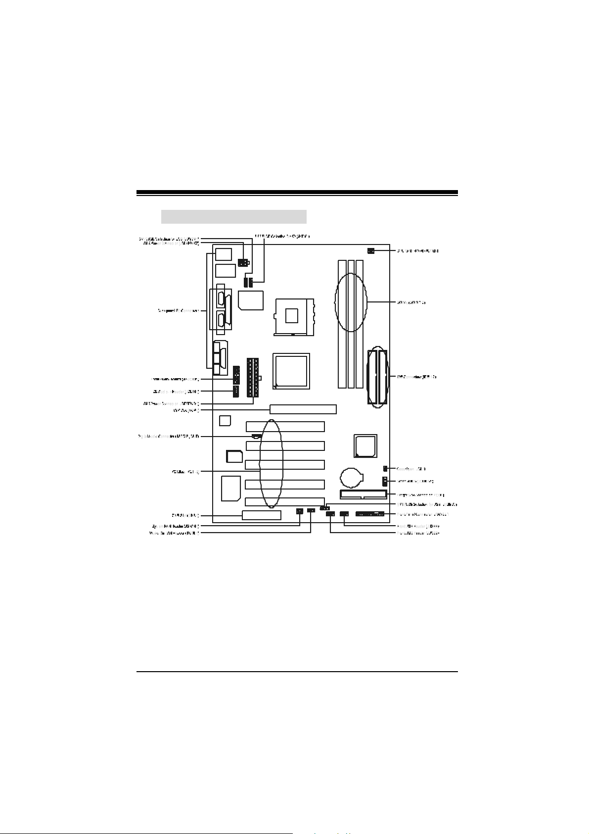
2-1. Layout of U8798
JKBMS1
Mouse &
KB
JUSB1
USB
JCOM1
JCOM1
COM1COM2
JUSBV1
JUSBV1
1
1
ITE I/O
JATXP WR 2
JKBV1
1
CPU1
Socket 478
JCOM2
Sp-OutLin e-InMi c -I n
Ga m e Port
JAUDIO1
JCDIN1
CODEC
Har dware
Audio
Parallel Port
JPRNT1
JGAME1
12
13 1 4
BIO S
CNR1
1
1
CNR SLOT
JATXPWR1
PCI SLOT
JSPDIF_OUT
PCI SLOT
PCI SLOT
PCI SLOT
PCI SLOT
CP U
P4X400
AGP S LOT
1
JSFAN1
1
JWOL1
PCI1
PCI2
PCI2
PCI4
PCI5
1
JUSBV3
2910
1
JUSB2
2
JUSB3
DIMM2
DIMM1
DIMM3
PRI MARY IDE CONN.
VT 8235
2
1
JCMOS1
JPANEL 1
BAT1
FLOP PY DI S K CO NN.
10
91
JCL1
1
SECONDARY ID E CON N.
24
23
6

Mainboard Features
2-2. Co m pon ent I nd e x
CODEC
7

Mainboard Features
3 . CPU Confi guration
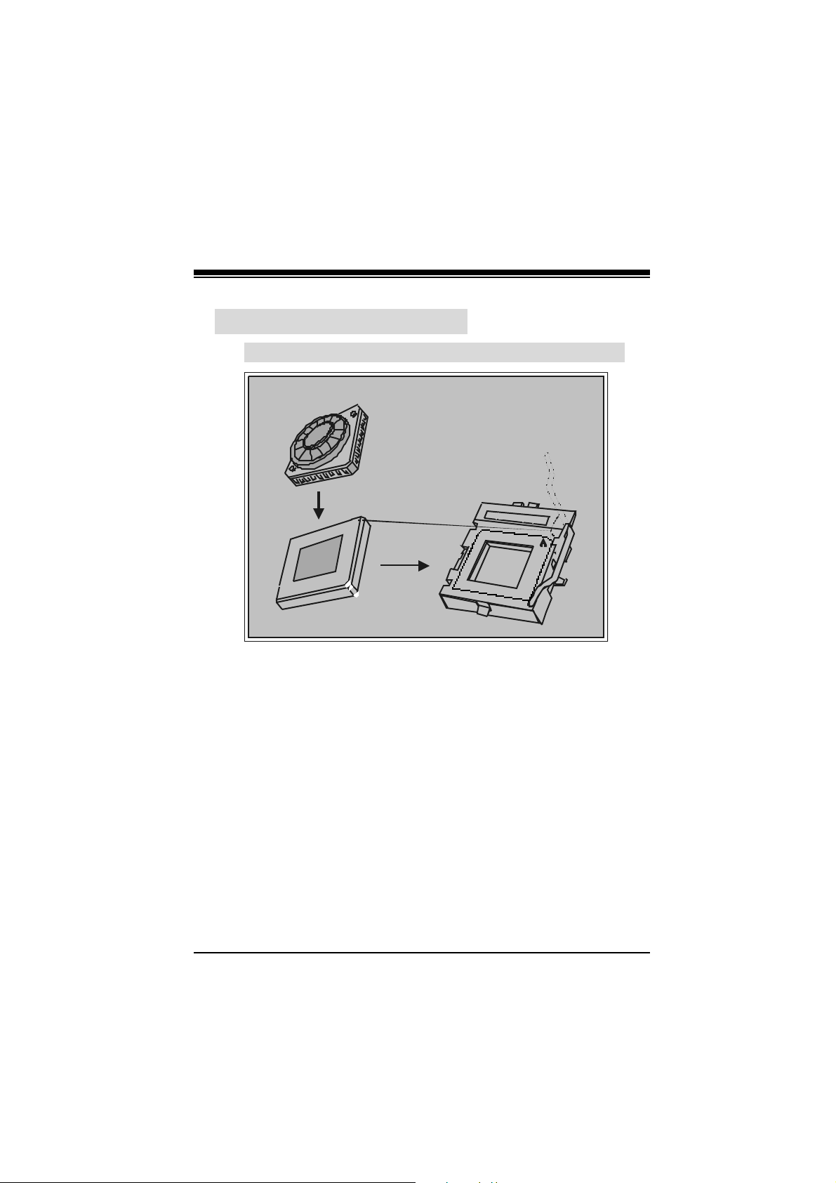
3-1. CPU Socket 478 Configuration Steps:
CPU Fan
CPU
1. Pull the lever sideways away from the socket then raise the
lever up to a 9 0 -degree angle.
2. Loc ate P in A in the socket and look for the white dot or c ut
ed ge i n the C PU . M atc h P in A w it h th e whi te do t /cu t e d ge
then insert the CPU.
3. Pr e ss th e l e ver do w n. Th en Put th e fan on the CP U a nd b u ckl e
it and put the fan’s power port into the JC FAN1, then to
complete the installation.
8

Mainboard Features
CPU Configuration Layout
CO DEC
BIOS
Hardw a re
Au dio
ITE I/O
Socket 478
CPU
P4X400
VT8235
BAT1
1
JSFAN1
9

Mainboard Features
3-2. CPU Fan Header: JCFAN1
Pin N o. Assi gnment
1 Ground
2 +12V
3 Sense
3-3. System Fan Header: JSFAN1
Pin N o. Assi gnment
1
2 +12V
3
Ground
Sense
10

Mainboard Features
4 . Jumpers, H eaders & Connectors
JUSBV1
1
JATXPWR2
JKBV1
1
JATXPWR1
1
JWOL1
JUSB V3
1
CODEC
BIOS
Hard ware
Audio
ITE I/O
CPU
P4X4 00
Socket 478
BAT1
VT82 35
IDE1-2
JCL1
1
JCMOS1
FDD1
JPANEL1
29110
JUSB 3
JUSB 2
2
10
9
1
11

Mainboard Features
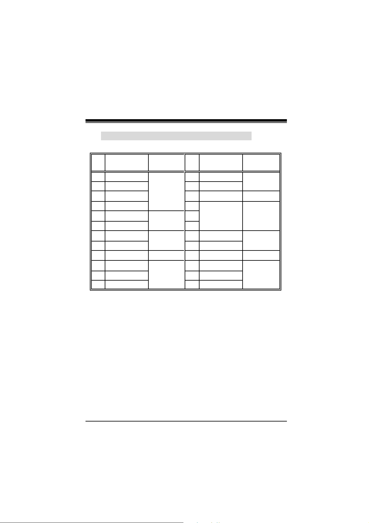
4-1. Fr o n t Pan el Connec tor: JPANEL 1
Pin Assignment Function Pin Assignment Function
No.
1
3
5
7
9
11
13
15
17
19
21
23
SPK (Sp eaker Connector)
An o ffboard speaker can be installe d on t he motherboard as a
manufacturing option. An o ffboard s peake r ca n be connected to
the motherboard at the front panel connector. The speaker
(onboard or offboard) provides error beep code information during
the Power On Se lf-Test when the computer cannot use the v ideo
i nte r fac e . T he s pea ker is n ot c on nected to th e a udio s ubs ys t em
and does not re c eive o utput from the audio subs ystem.
RST (Res e t Butto n )
This connector c an be attac hed to a momentary SPST switch. T his
switch is usually open and when closed will cause the
mot he r bo ard t o r eset a nd r un t he P OS T ( Pow er On Se lf Test) .
+5V 2 Sle ep C ontrol Sl e e p
NA Speaker 4 Ground Button
NA Connector
Speaker 8 Power LED (+)
HDD LED (+) Hard Dri ve
H D D L ED ( -) LED
Ground Reset
Reset Con trol Button
NA
NA IrDA
+5V Connector
IRTX
No.
6
Power LED (+) POWER
10
Power LED (-)
12
14
16
18
20
22
24
NA NA
LED
Power Butt on Power-on
Ground Button
KEY
KEY IrDA
Ground Connector
IRRX
12

Mainboard Features
POW-LED (Power LED Connector)
This connector can be attached to an LED on t he front panel of a
computer case. The LED will illuminate while the computer is
power e d on.
HLED (Hard Dri v e LED C on nector)
This connector can be attached to an LED on t he front panel of a
computer ca se. The LED will flicker dur ing disk a ctivity. This disk
ac tiv ity only applies to those IDE drives directly attached to the
system board.
IR (Infr ared Connector)
This connector is used to attach to a n infrared s e ns ing devic e.
After the IrDA interface is configured, connectionless data tra ns fer
to and from portable devices such as laptops, PDAs is possible.
SLP ( S leep / G reen Button)
This connector i s used to conserve energy b y poweri ng down the
monitor and the hard disk when not in use. To configure this
option, you need to connect a b utton from the front panel to this
connector. Depressing the button will power down the monitor
and hard drives until the system is invoked by any keyboard
ac tivity, mouse activity, modem activity or when the sle ep
button is depresse d again. APM (A dvanced Power Management)
mus t be enabled in the system BIOS and the APM driver must be
loaded.
ON/OFF ( Pow er Button)
This connector c an be attac hed to a front panel power switch. T he
switch m ust pull the Power Button pin to ground for at least 50 ms
to sign al the power suppl y to switch on or off. (The time requi red
is due to internal debounce circuitry on the system board). At
least two seconds must pass before the power supply will
recognize another on/of f signal.
13

Mainboard Features
t
t
4-2. ATX 20-pin Power Connector:
JATXPWR1
PIN Assignment PIN Assignment
1 +3 .3V 11 +3.3V
2 +3.3V 12 -12V
3 Ground 13 Ground
4 +5V 14 PS_ON
5 Ground 15 Ground
6 +5V 16 Ground
7 Ground 17 Ground
8 PW_OK 18 -5V
9 +5V_SB 19 +5V
10 +12V 20 +5V
4-3. ATX 12V Power Connector: JATXPWR2
PIN Assignmen
PIN Assignmen
1 +12V 3 Ground
2 +12V 4 Ground
14

Mainboard Features
4-4. H ar d D i sk C o n n e ct or s: I DE 1/ I DE2
T h is mai n bo ar d has a 3 2 -b i t E n ha nce d P C I I DE C on t rol ler t ha t
provides PIO Mode 0~4, Bus Master, and Ultra DMA / 33, Ult ra
DMA / 66,Ultra DMA / 100 functionality. It has two HDD
connectors IDE1 (prima ry) and IDE2 (s econdary).
• ID E1 (Pr imary IDE Connecto r)
The first hard drive should always be connected to IDE1. IDE1
can connect a Master and a S lave drive. Y ou must configure the
second hard drive o n IDE1 to Slave mode by setting the j umper
acco rdingly.
• ID E2 (Secondar y I DE Connector)
The IDE2 controller can also support a Master and a Slave drive.
The configuration is s imilar to IDE1. The second drive on this
con tro ll er m u st be set to sla ve mode.
4-5. Floppy Disk Connector: FDD1
The mot h erboard provides a standard floppy disk conn ector (FDC)
that sup ports 360K, 720K , 1.2M, 1 .44M and 2 .88M floppy disk
types. This connector s upports the provided floppy drive ribbon
cables.
4-6. Wake On LAN Header: JWOL1
Pin N o. Assi gnment
1
2 Ground
3
+5V_SB
Wake up
15

Mainboard Features
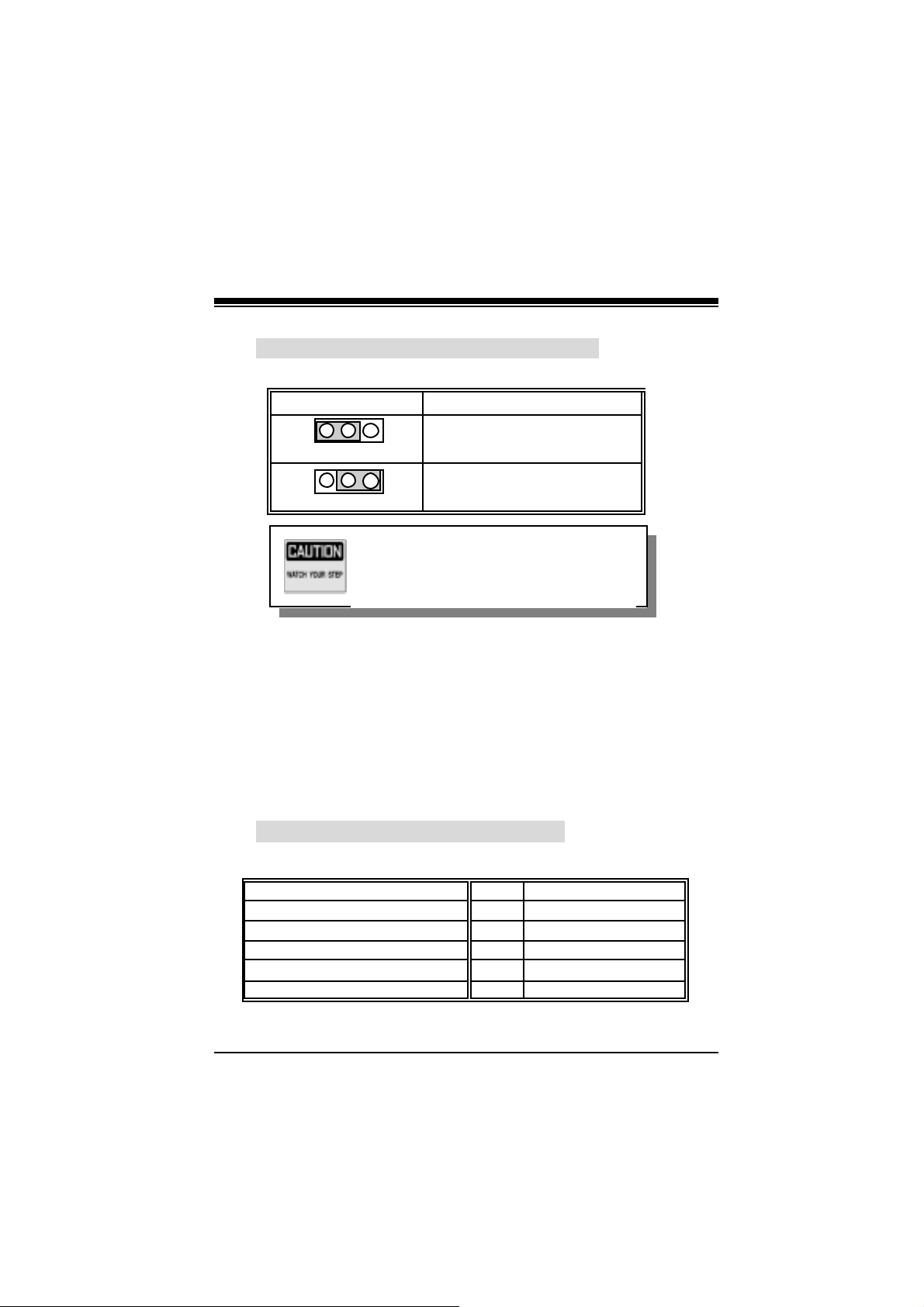
4-7. Clear CMOS Jumper: JCMOS1
JCMOS1 Assignment
1 3
1-2 Cl o sed
1 3
2-3 Cl o sed
Norm al Op e r at io n (d efau lt)
Cl ea r C M OS Da ta
T he following pr ocedures are f or resetting
the BIOS password. It is important to
follow these instructions closely.
※ Clear CMOS Procedures:
1. Remove AC power line.
2 . M ake JCMO S1 (2-3 ) c los ed.
3 . W a it for fiv e s ec onds .
4 . M ake JCMO S1 (1-2 ) c los ed.
5. Let AC power on.
6 . Reset your desired pass word or clear the CMO S data.
4-8. Fr o n t USB H ea d e r : JU SB3
(JUSB3)
Pin Assignment Pin Assignment
1 +5V(fused) 2 +5V (fused)
3 USBP2- 4 USBP3-
5 USBP2+ 6 USBP3+
7 Ground 8 Ground
9 KEY 10 NC
16
 Loading...