

Page 1

Federal Communications Commission
(F.C.C) Statement
This device complies with Part 15 of the FCC Rules. Operation of this
device is subject to the following two conditions: (1) this device may not
cause harmful interference, and (2) this device must accept any
interference received, including interference that may cause undesired
operation.
Accessories: This device has been tested and found to comply with the
limits of a Class B digital device, the accessories associated with this
equipment are as follows:
1. Shielded serial cable. (Can be obtained from multiple retail outlets)
2. Shielded printer cable. (Can be obtained from multiple retail outlets)
3. Shielded video cable. (Can be obtained from multiple retail outlets)
4. Shielded power cord. (Provided by manufacturer)
These accessories are required to ensure compliance with FCC Rules. It
is the responsibility of the user to provide and use these accessories
properly.
This equipment has been tested and found to comply with the limits of a
Class B digital device, pursuant to Part 15 of the FCC Rules. These limits
are designed to provide reasonable protection against harmful interference
in a residential installation. This equipment generates, uses and can
radiate radio frequency energy and, if not installed and used in accordance
with the instructions, may cause harmful interference to radio
communications. There is no guarantee that interference will not occur in
a particular installation. If this equipment does cause harmful interference
to radio or television reception, which can be determined by turning the
equipment off and on, you are encouraged to try to correct the
interference by one or more of the following measures:
1. Reorient / relocate the receiving antenna.
2. Increase the separation between the equipment and receiver.
3. Connect the equipment into an outlet on a circuit different from that
to which the receiver is connected.
4. Consult the dealer or an experienced radio/TV technician for help.
Caution: Changes or modifications not expressly approved by the
Page 2

manufacturer could void the user’s authority to operate the equipment.
Disclaimer
The vendor makes no representations or warranties with respect to the
contents here of and specially disclaims any implied warranties of
merchantability or fitness for any purpose. Further the vendor reserves the
right to revise this publication and to make changes to the contents here of
without obligation to notify any party beforehand.
Duplication of this publication, in part or in whole, is not allowed without
first obtaining the vendor’s approval in writing.
Trademarks and Remarks
MS-DOS, Windows NT, Windows 9X, Windows ME and Windows 2000
are products of Microsoft Corp, with its ownership of trademark, and are
distributed by the vendor under a license agreement. All trademarks used
in this manual are the property of their respective owners.
Copyright© 2001
All Rights Reserved
Canadian D.O.C. Statement
This digital apparatus does not exceed the Class B limits for radio noise emissions
from digital apparatus as set out in the radio interference regulations of the
Canadian Department of Communications.
Cet appareil numbérique n‘émet pas de bruits radioélectriques dépassant les
limites appliquées aux appareils numbériques de Class B préscrits dans le
réglement du brouillage radioélectrique edict par le minister Des Communications
du Canada.
Page 3

Contents
Introduction ................................................................................1-1
1. Motherboard Description ...................................................... 1-2
1.1 Features...................................................................................................1-2
1.1.1 Hardware.........................................................................................1-2
1.1.2 Software ..........................................................................................1-5
1.1.3 Attachments.....................................................................................1-5
1.2 Motherboard Installation.........................................................................1-6
1.2.1 Layout of Motherboard ...................................................................1-6
1.3 Motherboard Quick Reference................................................................1-7
1.3.1 Front Panel Connectors: JP8 / JPANEL1........................................1-8
1.3.2 Floppy Disk Connector: FDD1 .....................................................1-10
1.3.3 Hard Disk Connectors: IDE1/IDE2...............................................1-10
1.3.4 ATX 20-pin Power Connector: JATXPWR1 ................................1-11
1.4 Back Panel Connectors .........................................................................1-12
1.4.1 PS/2 Mouse / Keyboard Connector: JKBMS1 ..............................1-12
1.4.2 USB Connector: JUSB1................................................................1-13
1.4.3 Front USB Header: JUSB2 ...........................................................1-14
1.5 Serial and Parallel Interface Ports.........................................................1-15
1.6 CPU Installation....................................................................................1-18
1.6.1 CPU Installation Procedure: Socket A .......................................... 1-18
1.6.2 CPU Jumper Setting......................................................................1-19
1.6.2.1 CPU Frequency Selections: JCLK1 & JCLK2.................................. 1-20
i
Page 4

Contents
1.7 Jumper Setting.......................................................................................1-21
1.7.1 CPU Fan Header: JCFAN1 ...........................................................1-22
1.7.2 System Fan Header: JSFAN1 ........................................................1-22
1.7.3 System Fan Header: JSFAN3 ........................................................1-22
1.7.4 Wake-On-MODEM Header: JWOM1 (Optional)......................... 1-22
1.7.5 Wake-On-LAN Header: JWOL1...................................................1-23
1.7.6 AMR Code Primary/Secondary Selection: J4 ...............................1-23
1.7.7 SPK (Speaker Header): JP5 ..........................................................1-23
1.7.8 CMOS Function Selection: JCMOS1............................................1-24
1.8 DRAM Installation................................................................................1-25
1.8.1 DIMM ...........................................................................................1-25
1.8.2 How to install a DIMM Module....................................................1-27
1.9 Audio Subsystem...................................................................................1-28
1.9.1 CD Audio-In Headers: JCDIN1/JCDIN2 ......................................1-29
1.9.2 Telephony Header: JTAD1 ...........................................................1-29
1.9.3 AUX Audio in Header: JAUX1 (Optional)...................................1-29
1.9.4 Front Audio Header: JF_AUDIO (Optional).................................1-30
2. BIOS Setup.............................................................................. 2-1
2.1 Main Menu..............................................................................................2-3
2.2 Standard CMOS Features........................................................................2-6
2.3 Advanced BIOS Features........................................................................2-9
2.4 Advanced Chipset Features...................................................................2-13
2.5 Integrated Peripherals ...........................................................................2-17
ii
Page 5

Contents
2.6 Power Management Setup.....................................................................2-22
2.7 PnP/PCI Configurations........................................................................2-27
2.8 PC Health Status ...................................................................................2-30
2.9 Frequency / Clock Control ....................................................................2-31
2.10 Load Fail-Safe Defaults ......................................................................2-32
2.11 Load Optimized Defaults....................................................................2-33
2.12 Set Supervisor / User Password ..........................................................2-34
2.13 Save & Exit Setup...............................................................................2-36
2.14 Exit Without Saving............................................................................2-37
3. Trouble Shooting .................................................................... 3-1
iii
Page 6

Chapter 1 Motherboard Description
Introduction
System Overview
Thanks for buying this product! This manual was written to help you start using this
product as quickly and smoothly as possible. Inside you will find adequate
explanations to solve most problems. In order for this reference material to be of
greatest use, refer to the “expanded table of contents” to find relevant topics.
This board incorporates the system board, I/O, and PCI IDE into one board that
provides a total PC solution. The mainboard, AMD Athlon
processor based PC ATX system, supports single processors with ISA Bus, PCI
Local Bus, and AGP Bus to support upgrades to your system performance. It is
ideal for multi-tasking and fully supports MS-DOS, Windows NT, Windows 2000,
Novell, Windows95/98, Windows ME, LINUX, UNIX, SCO UNIX etc. This
manual also explains how to install the mainboard for operation, and how to setup
your CMOS configuration with the BIOS setup program.
TM
and DuronTM
1-1
Page 7

Chapter 1 Motherboard Description
1. Motherboard Description
1.1 Features
1.1.1 Hardware
CPU
Single AMD Socket-A for Athlon
−
processor Module-500MHz ~ 1.2GHz.
200/266MHz Front Side Bus.
−
Speed
Support 33MHz PCI Bus speed.
−
Support 4X AGP Bus.
−
DRAM Memory
Supports 8/16/32/64/128/256MB DIMM module.
−
Supports Synchronous DRAM (3.3V).
−
Support a maximum memory size of 768MB with SDRAM.
−
Shadow RAM
A memory controller provide shadow RAM and supports 8-bit ROM
−
BIOS.
Green Function
Support power management operation via BIOS.
−
Power down timer from 1 to 15 mins.
−
Wakes from power saving sleep mode at the press of any key or any
−
mouse activity.
BUS Slots
Provide one AGP slot and one AMR slot.
−
Five 32-bit PCI bus and one ISA slot bus master slots.
−
TM
(Thunderbird
TM
) / Duron
TM
Flash Memory
Support flash memory.
−
Support ESCD Function.
−
1-2
Page 8

Chapter 1 Motherboard Description
IDE Built-in On Board
Supports four IDE hard disk drives.
−
Supports PIO Mode 4, Master Mode, high performance hard disk drives.
−
Support Ultra DMA 33, 66, 100 (Optional) Bus Master Mode.
−
Supports IDE interface with CD-ROM.
−
Supports high capacity hard disk drives.
−
Support LBA mode.
−
Stereo AC 97 Digital Audio codec
AC 97 2.1 interface.
−
16 channels of high-quality sample rate conversion.
−
16x8 channel digital mixer.
−
Stereo 10 band graphic equalizer.
−
Sound Blaster® and Sound Blaster Pro® emulation.
−
64-voice wavetable.
−
PC99 complaint and WHQL certified.
−
I/O Built-in On Board
Supports one multi-mode Parallel Port.
−
(1) Standard & Bidirection Parallel Port.
(2) Enhanced Parallel Port (EPP).
(3) Extended Capabilities Port (ECP).
Supports two serial ports, 16550 UART.
−
Supports one Infrared transmission (IR).
−
Supports PS/2 mouse and PS/2 keyboard.
−
Supports 360KB, 720KB, 1.2MB, 1.44MB, and 2.88MB floppy disk
−
drivers.
HW Sound CT5880 (Optional)
128 voice PCI wave-table synthesis.
−
EAX Support.
−
Four Speaker support.
−
Real Mode DOS Game Compatibility w/ no ISA bus pins required.
−
CD audio over the PCI bus (CDDA).
−
Tone Control.
−
Speaker EQ.
−
Mixing of Analong inputs routed to SPDIF out for PCM data.
−
PCI Bus Master for fast DMA.
−
1-3
Page 9

Chapter 1 Motherboard Description
Uses a single sharable PCI Interrupt.
−
Multiple sample rate support.
−
Sounds are stored in Host memory.
−
Sound Library of over 4000 Sounds.
−
3 Stereo inputs and 3 mono inputs can be mixed into the output stream.
−
Direct I/O space access of the control registers.
−
100 Pin PQFP.
−
AC97 2.1 interface.
−
5V Power.
−
ACPI Support.
−
Fully Compliant with PC97 Power Management specification.
−
Universal Serial Bus
Supports two back Universal Serial Bus (USB) Ports and two front
−
Universal serial Bus (USB) Ports.
Supports 48 MHz USB.
−
Hardware Monitor Function
CPU Fan Speed Monitor.
−
System and CPU Temperature Monitor. (Optional)
−
System Voltage Monitor.
−
Dimensions (ATX form-factor)
22.2 cm X 30.5 cm (W x L)
−
1-4
Page 10

Chapter 1 Motherboard Description
1.1.2 Software
BIOS
AWARD legal BIOS.
−
Supports APM1.2.
−
Supports USB Function.
−
Supports ACPI.
−
Operating System
Offers the highest performance for MS-DOS, Windows NT, Windows
−
2000, Windows 95/98, Windows ME, Novell, LINUX7.0, UNIX, SCO
UNIX etc.
1.1.3 Attachments
HDD Cable.
−
FDD Cable.
−
Flash Memory Writer for BIOS Update.(Include in CD Driver)
−
USB2 Cable (Optional).
−
Rear I/O Panel for ATX Case (Optional).
−
Fully Setup Driver CD.
−
Chipset Fan (Optional).
−
For 1.2GHz CPU and above, we recommend the user to
add a “Chipset Fan” in order to reduce the excess thermal
dissipated from Northbridge Chipset.
1-5
Page 11
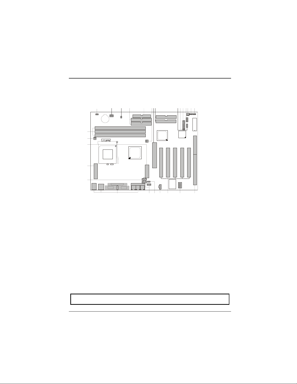
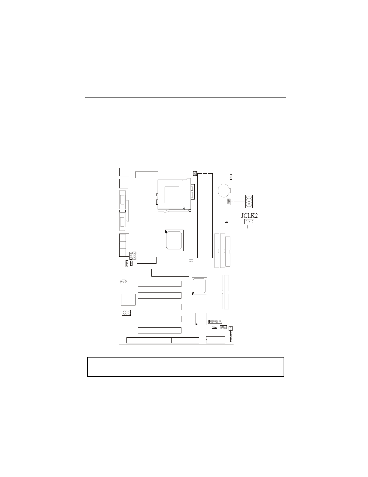
Chapter 1 Motherboard Description
1.2 Motherboard Installation
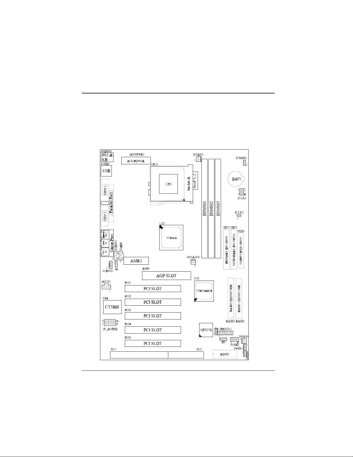
1.2.1 Layout of Motherboard
Model No.M7VKD
1-6
Page 12
Chapter 1 Motherboard Description
1.3 Motherboard Quick Reference
T
U
SV
W
X
Y
Z
A1
ABCDEFG
A. Back Panel I/O Connectors N. Speaker Header (JP5)
B. CD Audio-In Headers (JCDIN1-2) O. RAID Connectors (
C. AMR CODEC Primary / Secondary P. AGP BUS Slot (AGP1)
Selection (J4) Q. Chipset Fan Header (
D. AUX Audio-In Header (
E. PCI BUS Slots (PCI1-5) S. IDE Connectors (IDE1-2)
F. Front Audio Header (
G. ISA BUS Slot (SL1-2) U. CPU Frequency Selection (JCLK1)
H. Wake-On-MODEM Header (
I. Wake-On-LAN Header (JWOL1) W. DIMMs (DIMM1-3)
J. System Fan Header (JSFAN1) X. CPU Fan Header (JCFAN1)
K. Front USB Header (JUSB2) Y. AMR BUS Slot (AMR1)
L. Front Panel Header (JPANEL1) Z. ATX Power Connector (JATXPWR1)
M. Co-Front Panel Header (JP8) A1. Telephony Header (JTAD1)
JAUX1) R. FDD Connector (FDD1)
JF_AUDIO) T. CPU Ratio Selection (JCLK2)
JWOM1) V. CMOS Function Selection (JCMOS1)
Q
HIJKLMNOPR
RAID1-2)
JSFAN3)
Note: The “
“mark represent the function is optional.
1-7
Page 13
Chapter 1 Motherboard Description
1.3.1 Front Panel Connectors: JP8 / JPANEL1
JP8
Note: The JP8 (pin1) & JPANEL1 (pin4) Connectors can support 3-pin Power LED
JPANEL1
Pin NO. Assignment Function Pin NO. Assignment Function
1
HDD LED (+) Hard Drive
3
HDD LED (-) LED
5
7
Reset Control Button
9
11
13
15
17
JP8 JPANEL1
2
2
1
1
PW/SLP
LED
HDLED
PW-BN
RESET
2
4
6
8
10
12
14
16
18
SLP-BN
Power LED (+) LED
No Connection No Connection
+5V
IrDA
Power LED (-)
Ground
Power LED (-) Power
Power Button Power
Ground Button
Sleep Control Sleep
Ground Button
+5V Power
NC NC
Po wer LE D (-)
1
2
Ground
Pin No. Assignment
1
2
Ground Reset
+5V
Ir-In IrDA
Ground Connector
Ir-Out
NC NC
NCKey
18
17
NC
1-8
Page 14

Chapter 1 Motherboard Description
Speaker Connector
An offboard speaker can be installed on the motherboard as a manufacturing option.
An offboard speaker can be connected to the motherboard at the front panel
connector. The speaker (onboard or offboard) provides error beep code information
during the Power On Self-Test when the computer cannot use the video interface.
The speaker is not connected to the audio subsystem and does not receive output
from the audio subsystem.
Reset Button
This connector can be connected to a momentary SPST type switch that is normally
open. When the switch is closed, the motherboard resets and runs the POST.
Power LED Connector
This connector can be connected to an LED that will light when the computer is
powered on.
Hard Drive LED Connector
This connector can be connected to an LED to provide a visual indicator that data is
being read from or written to a hard drive. For the LED to function properly, an
IDE drive must be connected to the onboard hard drive controller.
Infrared Connector
After the IrDA interface is configured, files can be transferred from or to portable
devices such as laptops, PDAs, and printers using application software.
Sleep Button
When APM is enabled in the system BIOS, and the operating system’s APM driver
is loaded, the system can enter sleep (standby) mode in one of the following ways:
•
Optional front panel SMI button
•
Prolonged system inactivity using the BIOS inactivity timer feature
he 2-pin header located on the front panel I/O connector supports a front panel
T
SMI switch, which must be a momentary SPST type that is normally open.
Closing the SMI switch sends a System Management Interrupt (SMI) to the
processor, which immediately goes into System Management Mode (SMM).While
the computer is in sleep mode it is fully capable of responding to and servicing
external interrupts (such as an incoming fax) even though the monitor turns on only
if a keyboard or mouse interrupt occurs. To reactivate or resume the system, the
SMI switch must be pressed again, or the keyboard or mouse must be used.
1-9
Page 15

Chapter 1 Motherboard Description
Power On Button
This connector can be connected to a front panel power switch. The switch must
pull the Power Button pin to ground for at least 50 ms to signal the power supply to
switch on or off. (The time requirement is due to internal debounce circuitry on the
motherboard). At least two seconds must pass before the power supply will
recognize another on/off signal.
1.3.2 Floppy Disk Connector: FDD1
The motherboard provides a standard floppy disk connector (FDC) that supports
360K, 720K, 1.2M, 1.44M and 2.88M floppy disk types. This connector supports
the provided floppy drive ribbon cables.
1.3.3 Hard Disk Connectors: IDE1/IDE2
The motherboard has a 32-bit Enhanced PCI IDE Controller that provides PIO
Mode 0~4, Bus Master, and Ultra DMA / 33, Ultra DMA / 66, Ultra DMA/100
(Optional) functionality. It has two HDD connectors IDE1 (primary) and IDE2
(secondary). You can connect up to four hard disk drives, a CD-ROM, a 120MB
Floppy (reserved for future BIOS) and other devices to IDE1 and IDE2. These
connectors support the IDE hard disk cable provided.
•
IDE1 (Primary IDE Connector)
The first hard drive should always be connected to IDE1. IDE1 can connect a
Master and a Slave drive. You must configure the second hard drive on IDE1 to
Slave mode by setting the jumper accordingly.
•
IDE2 (Secondary IDE Connector)
The IDE2 controller can also support a Master and a Slave drive. The configuration
is similar to IDE1. The second drive on this controller must be set to slave mode.
1-10
Page 16

Chapter 1 Motherboard Description
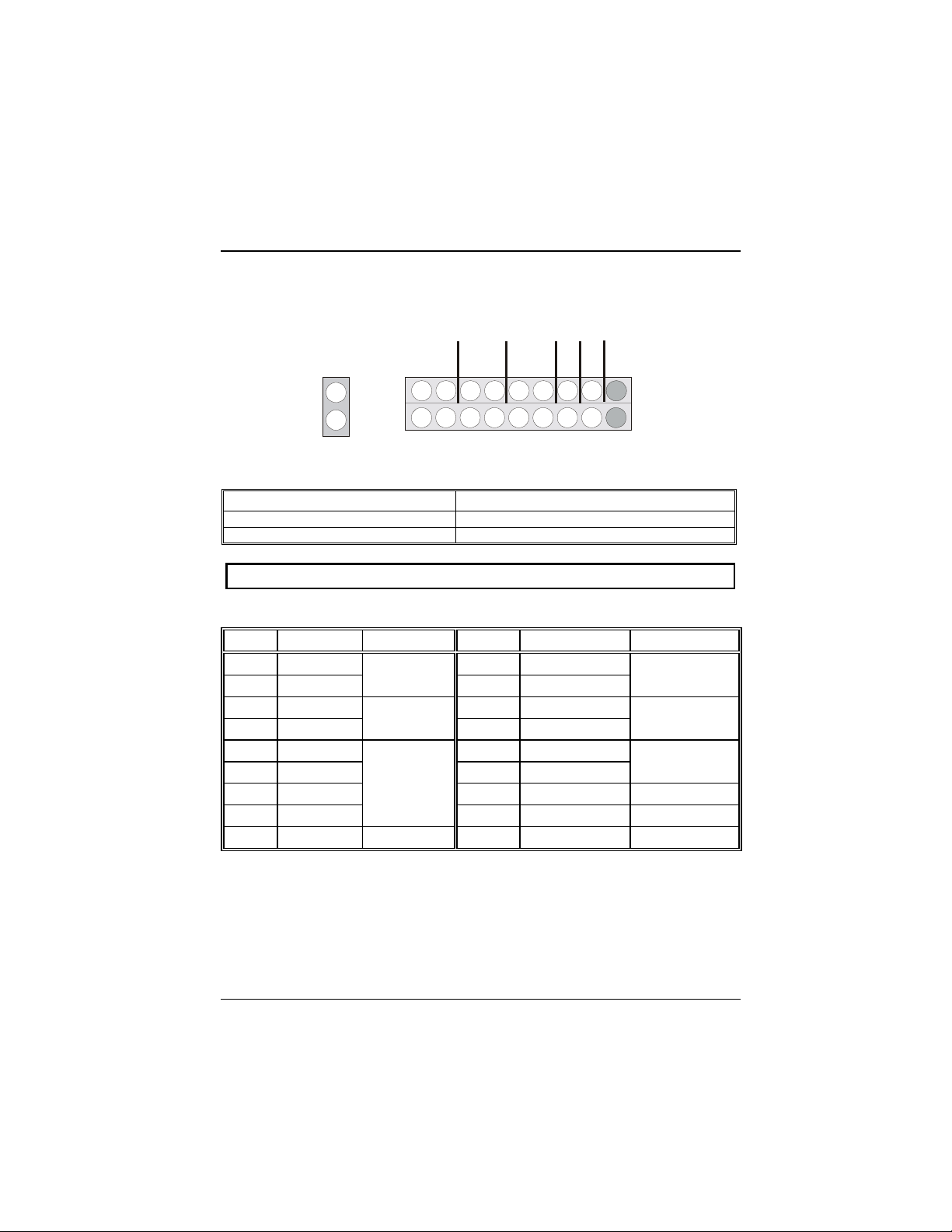
1.3.4 ATX 20-pin Power Connector: JATXPWR1
This connector supports the power button on-board. Using the ATX power
supply, functions such as Modem Ring Wake-Up and Soft Power Off are supported
on this motherboard. This power connector supports instant power-on functionality,
which means that the system will boot up instantly when the power connector is
inserted on the board.
PIN Assignment PIN Assignment
1 3.3V 11 3.3V
2 3.3V 12 -12V
3 Ground 13 Ground
4 5V 14 PS_ON
5 Ground 15 Ground
6 5V 16 Ground
7 Ground 17 Ground
8 PW_OK 18 -5V
9 5V_SB 19 5V
10 12V 20 5V
1-11
Page 17
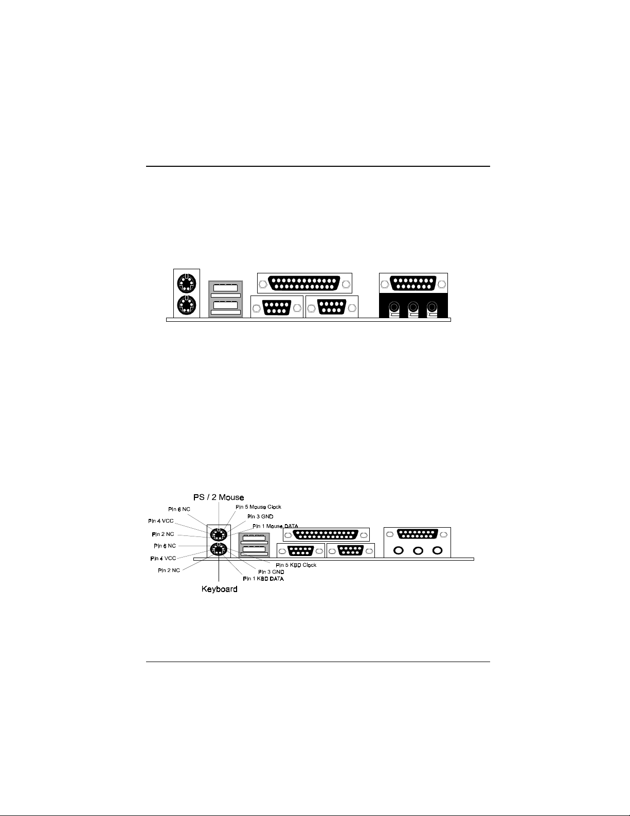
Chapter 1 Motherboard Description
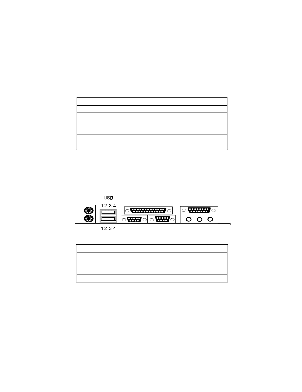
1.4 Back Panel Connectors
P S /2
Mouse
PS/2
Keyboard
USB
Parallel Port
COM1 COM2
1.4.1 PS/2 Mouse / Keyboard Connector: JKBMS1
The motherboard provides a standard PS/2 mouse / Keyboard mini DIN connector
for attaching a PS/2 mouse. You can plug a PS/2 mouse / Keyboard directly into
this connector. The connector location and pin definition are shown below:
Game Port
Speaker
out
Line
in
Mic
in
1-12
Page 18
Chapter 1 Motherboard Description
PS/2 Mouse / Keyboard Connectors
Pin Assignment
1 Data
2 No connect
3 Ground
4 +5 V
5 Clock
6 No connect
1.4.2 USB Connector: JUSB1
The motherboard provides a
Serial Bus Roots
USB devices. You can plug the USB devices directly into this connector.
for attaching USB devices such as: keyboard, mouse and other
OHCI (Open Host Controller Interface) Universal
Stacked USB Connector
Pin Assignment
1 +5 V
2 USBP0- [USBP1-]
3 USBP0+ [USBP1+]
4 Ground
Signal names in brackets (
) are for USB Port 1.
1-13
Page 19
Chapter 1 Motherboard Description
1.4.3 Front USB Header: JUSB2
Pin Assignment Pin Assignment
1
3
5
7
9
+5V
USBP2-
USBP2+
Ground
Ground
2
4
6
8
10
JUSB2
Ground
Ground
USBP3+
USBP3-
+5V
1
9
1-14
Page 20
Chapter 1 Motherboard Description
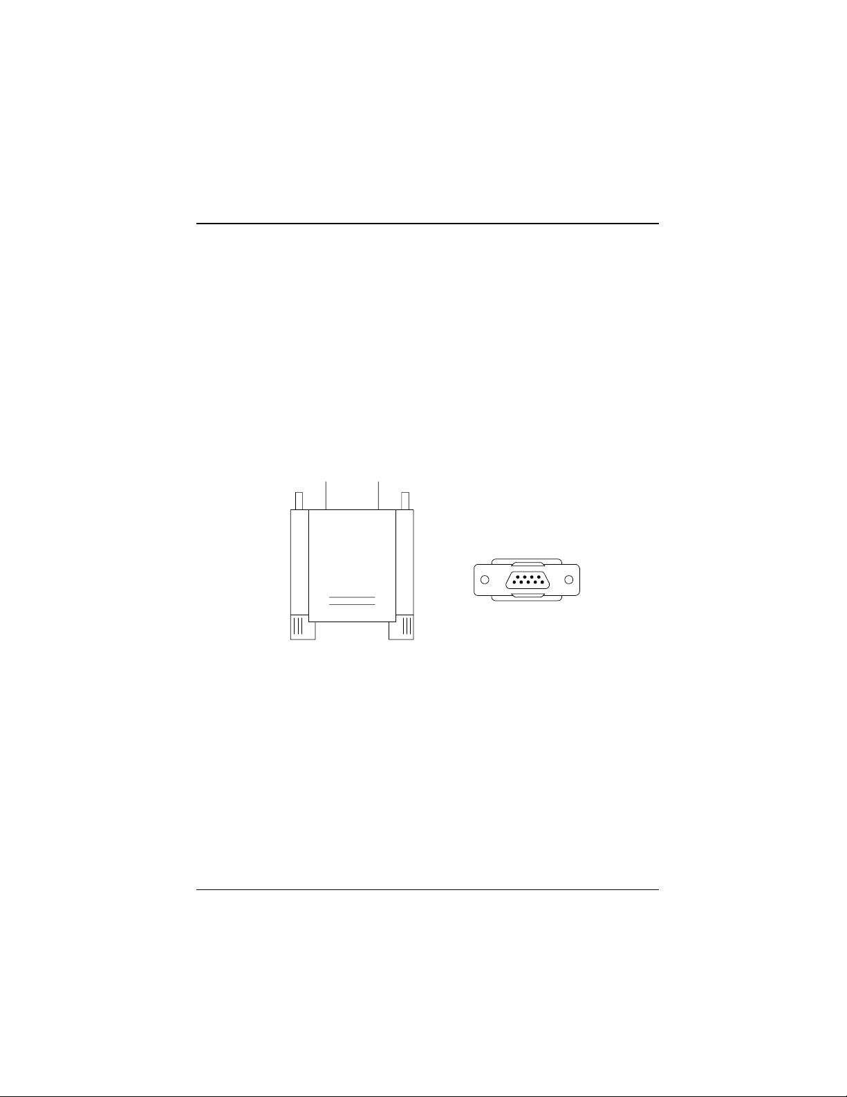
1.5 Serial and Parallel Interface Ports
This system comes equipped with two serial ports and one parallel port. Both types
of interface ports will be explained in this chapter.
The Serial Interface: COM1/COM2
The serial interface port is sometimes referred to as an RS-232 port or an
asynchronous communication port. Mice, printers, modems and other peripheral
devices can be connected to a serial port. The serial port can also be used to
connect your computer with another computer system. If you wish to transfer the
contents of your hard disk to another system it can be accomplished by using each
machine’s serial port.
The serial ports on this system have two 9-pin connectors. Some older computer
systems and peripherals used to be equipped with only one 25-pin connector.
Should you need to connect your 9-pin serial port to an older 25-pin serial port, you
can purchase a 9-to-25 pin adapter.
1-15
Page 21

Chapter 1 Motherboard Description
Connectivity
The serial ports can be used in many ways, and it may be necessary to become
familiar with the pinout diagram. The following chart gives you the function of
each pin on the 9-pin connector and some of the 25-pin connector. This information
can be used when configuring certain software programs to work with the serial
ports.
Signal Name DB9 PIN DB25 PIN
DCD Data Carrier Detect 1 8
RX Receive Data 2 3
TX Transmit Data 3 2
DTR Data Terminal Ready 4 20
GND Signal Ground 5 7
DSR Data Set Ready 6 6
RTS Request to Send 7 4
CTS Clear to Send 8 5
RI Ring Indicator 9 22
1-16
Page 22
Chapter 1 Motherboard Description
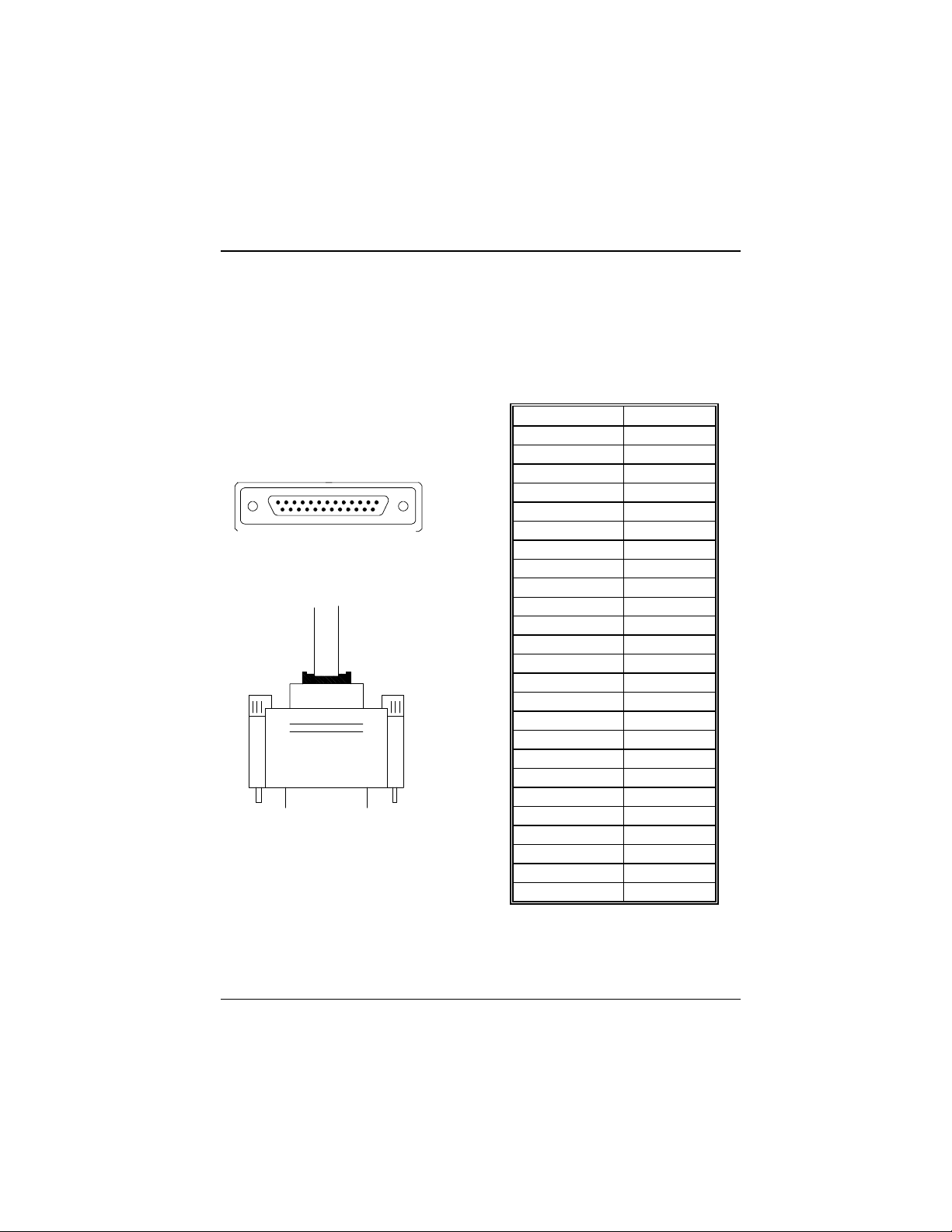
Parallel Interface Ports
Unlike the serial ports, parallel interface port has been standardized and should not
present any difficulty interfacing peripherals to your system. Sometimes called
Centronics port, the parallel port is almost exclusively used with printers. The
parallel port on your system has a 25-pin, DB25 connector (see picture below). The
pinouts for the parallel port are shown in the table below.
Signal Pin
-Strobe 1
Data 0 2
Data 1 3
Data 2 4
Data 3 5
Data 4 6
Data 5 7
Data 6 8
Data 7 9
-Ack 10
Busy 11
Paper Empty 12
+Select 13
-Auto FDXT 14
-Error 15
-Init 16
-SLCTN 17
Ground 18
Ground 19
Ground 20
Ground 21
Ground 22
Ground 23
Ground 24
Ground 25
1-17
Page 23

Chapter 1 Motherboard Description
1.6 CPU Installation
1.6.1 CPU Installation Procedure: Socket A
1. Pull the lever sideways away from the socket then raise the lever up to
a 90-degree angle.
2. Locate Pin A in the socket and look for the white dot or cut edge in the
CPU. Match Pin A with the white dot/cut edge then insert the CPU.
3. Press the lever down to complete the installation.
1-18
Page 24
Chapter 1 Motherboard Description
1.6.2 CPU Jumper Setting
This motherboard produces a feature, which can auto-detect the speed without
jumper setting. Also, you can use the JCLK1 and JCLK2 jumpers to set the
appropriately speed of CPU when the auto-detect function is disabled.
This section describes how to configure the CPU jumpers by manual to match the
characteristics of the CPU you have installed on your motherboard.
JCLK1
2
1
8
7
NOTES: JCLK1 and JCLK2 tables are available by Hardware setting
when BIOS setting is useless or disabled.
1-19
Page 25

Chapter 1 Motherboard Description
1.6.2.1 CPU Frequency Selections: JCLK1 & JCLK2
(JCLK1)
JCLK1
1-2 3-4 5-6 7-8
FREQ.
100MHz
*
133MHz
ON OFF OFF OFF
ON OFF ON OFF
(JCLK2)
CPU (MHz) JCLK2
100MHz
*
133MHz
NOTES: The “ * ” mark indicate primitive value.
ON
OFF
1-20
Page 26

Chapter 1 Motherboard Description
1.7 Jumper Setting
A jumper has two or more pins that can be covered by a plastic jumper cap,
allowing you to select different system options.
1-21
Page 27

Chapter 1 Motherboard Description
1.7.1 CPU Fan Header: JCFAN1
Pin No. Assignment
1
2
3
1.7.2 System Fan Header: JSFAN1
Ground
+12V
Sensor
Pin No. Assignment
1
2
3
1.7.3 System Fan Header: JSFAN3
Ground
+12V
Sensor
Pin No. Assignment
1
2
3
1.7.4 Wake-On-MODEM Header: JWOM1 (Optional)
Ground
+12V
Ground
Pin No. Assignment
1
2
3
5V_SB
Ground
Wake Up
1-22
Page 28

Chapter 1 Motherboard Description
1.7.5 Wake-On-LAN Header: JWOL1
Pin No. Assignment
1
2
3
5V_SB
Ground
Wake up
1.7.6 AMR Code Primary/Secondary Selection: J4
Pin No. Assignment
1-2
2-3
Secondary
Primary
1.7.7 SPK (Speaker Header): JP5
Pin No. Assignment
1
2
3
4
+5V
No Connection
No Connection
Speaker
1-23
Page 29

Chapter 1 Motherboard Description
1.7.8 CMOS Function Selection: JCMOS1
JCMOS1 Assignment
1 3
1-2 Closed
1 3
2-3 Closed
Normal Operation (default)
Clear CMOS Data
Please follow the procedure as below to clear CMOS
Note:
data.
Please follow the procedure as below to clear BIOS
Note:
password if your password is lost or forgotten.
Remove AC
power line
JCMOS1
(2-3) closed
Wait ten
seconds
Reset your desired password
AC power on
or clear CMOS data
JCMOS1
(1-2) closed
1-24
Page 30

Chapter 1 Motherboard Description
1.8 DRAM Installation
1.8.1 DIMM
DRAM Access Time : 3.3V Unbuffered SDRAM PC100 and PC133 Type
required.
DRAM Type : 8MB/ 16MB/ 32MB/ 64MB/ 128MB/ 256MB DIMM Module
(168pin).
Total Bank 0 Bank 1 Bank 2
Memory Size (MB) DIMM1 DIMM2 DIMM3
8 M 8M x 1 pc ---- ---16 M 16M x 1 pc ---- ---32 M 32M x 1 pc ---- ---64 M 64M x 1 pc ---- ----
128 M 128M x 1 pc ---- ---256 M 256M x 1 pc ---- ----
16 M 8M x 1 pc 8M x 1 pc ---32 M 16M x 1 pc 16M x 1 pc ---64 M 32M x 1 pc 32M x 1 pc ----
128 M 64M x 1 pc 64M x 1 pc ---256 M 128M x 1 pc 128M x 1 pc ---512 M 256M x 1 pc 256M x 1 pc ----
24 M 8M x 1 pc 8M x 1 pc 8M x 1 pc
40 M 16M x 1 pc 16M x 1 pc 8M x 1 pc
72 M 32M x 1 pc 32M x 1 pc 8M x 1 pc
136 M 64M x 1 pc 64M x 1 pc 8M x 1 pc
264 M 128M x 1 pc 128M x 1 pc 8M x 1 pc
520 M 256M x 1 pc 256M x 1 pc 8M x 1 pc
32 M 8M x 1 pc 8M x 1 pc 16M x 1 pc
48 M 16M x 1 pc 16M x 1 pc 16M x 1 pc
80 M 32M x 1 pc 32M x 1 pc 16M x 1 pc
144 M 64M x 1 pc 64M x 1 pc 16M x 1 pc
272 M 128M x 1 pc 128M x 1 pc 16M x 1 pc
528 M 256M x 1 pc 256M x 1 pc 16M x 1 pc
1-25
Page 31

Chapter 1 Motherboard Description
Total Bank 0 Bank 1 Bank 2
Memory Size (MB) DIMM1 DIMM2 DIMM3
48 M 8M x 1 pc 8M x 1 pc 32M x 1 pc
64 M 16M x 1 pc 16M x 1 pc 32M x 1 pc
96 M 32M x 1 pc 32M x 1 pc 32M x 1 pc
160 M 64M x 1 pc 64M x 1 pc 32M x 1 pc
288 M 128M x 1 pc 128M x 1 pc 32M x 1 pc
544 M 256M x 1 pc 256M x 1 pc 32M x 1 pc
80 M 8M x 1 pc 8M x 1 pc 64M x 1 pc
96 M 16M x 1 pc 16M x 1 pc 64M x 1 pc
128 M 32M x 1 pc 32M x 1 pc 64M x 1 pc
192 M 64M x 1 pc 64M x 1 pc 64M x 1 pc
320 M 128M x 1 pc 128M x 1 pc 64M x 1 pc
576 M 256M x 1 pc 256M x 1 pc 64M x 1 pc
144 M 8M x 1 pc 8M x 1 pc 128M x 1 pc
160 M 16M x 1 pc 16M x 1 pc 128M x 1 pc
192 M 32M x 1 pc 32M x 1 pc 128M x 1 pc
256 M 64M x 1 pc 64M x 1 pc 128M x 1 pc
384 M 128M x 1 pc 128M x 1 pc 128M x 1 pc
640 M 256M x 1 pc 256M x 1 pc 128M x 1 pc
272 M 8M x 1 pc 8M x 1 pc 256M x 1 pc
288 M 16M x 1 pc 16M x 1 pc 256M x 1 pc
320 M 32M x 1 pc 32M x 1 pc 256M x 1 pc
384 M 64M x 1 pc 64M x 1 pc 256M x 1 pc
512 M 128M x 1 pc 128M x 1 pc 256M x 1 pc
768 M 256M x 1 pc 256M x 1 pc 256M x 1 pc
*The list shown above for DRAM configuration is only for reference.
1-26
Page 32

Chapter 1 Motherboard Description
1.8.2 How to install a DIMM Module
1. The DIMM socket has a “ Plastic
Safety Tab” and the DIMM memory
module has an asymmetrical notch”,
so the DIMM memory module can
only fit into the slot in one direction.
2. Push the tabs out. Insert the DIMM
memory modules into the socket at a
90-degree angle then push down
vertically so that it will fit into place.
3. The Mounting Holes and plastic
tabs should fit over the edge and hold
the DIMM memory modules in place.
Single Sided DIMM
Double Sided DIMM
1-27
Page 33

Chapter 1 Motherboard Description
1.9 Audio Subsystem
JTAD1
1
JCDIN1
1
JCDIN2
1
1
JAU X 1
2
1
JF_A UD IO
10
9
1-28
Page 34

Chapter 1 Motherboard Description
1.9.1 CD Audio-In Headers: JCDIN1/JCDIN2
Pin No. of JCDIN1 Assignment
1
2
3
4
Left Channel Input
Ground
Ground
Right Channel Input
Pin No. of JCDIN2 Assignment
1
2
3
4
1.9.2 Telephony Header: JTAD1
Ground
Left Channel Input
Ground
Right Channel Input
Pin No. Assignment
1
2
3
4
1.9.3 AUX Audio in Header: JAUX1 (Optional)
MONO_IN
Ground
Ground
MONO_OUT
Pin No. Assignment
1
2
3
4
Left channel AUX_IN
Ground
Ground
Right channel AUX_IN
1-29
Page 35

Chapter 1 Motherboard Description
1.9.4 Front Audio Header: JF_AUDIO (Optional)
Pin Assignment Pin Assignment
1
3
5
7
9
Line_out_L
Ground
Line_in_L
Ground
MIC_in
2
4
6
8
10
Line_out_R
Ground
Line_in_R
Pin Removed as key pin
Ground
1-30
Page 36

Chapter2 BIOS Setup
2. BIOS Setup
Introduction
This manual discussed Award™ Setup program built into the ROM BIOS. The
Setup program allows users to modify the basic system configuration. This special
information is then stored in battery-backed RAM so that it retains the Setup
information when the power is turned off.
The Award BIOS™ installed in your computer system’s ROM (Read Only
Memory) is a custom version of an industry standard BIOS. This means that it
supports AMD-Athlon
provides critical low-level support for standard devices such as disk drives and
serial and parallel ports.
Adding important has customized the Award BIOS™, but nonstandard, features
such as virus and password protection as well as special support for detailed
fine-tuning of the chipset controlling the entire system.
The rest of this manual is intended to guide you through the process of
configuring your system using Setup.
Plug and Play Support
These AWARD BIOS supports the Plug and Play Version 1.0A specification.
ESCD (Extended System Configuration Data) write is supported.
EPA Green PC Support
This AWARD BIOS supports Version 1.03 of the EPA Green PC specification.
APM Support
These AWARD BIOS supports Version 1.1&1.2 of the Advanced Power
Management (APM) specification. Power management features are implemented
via the System Management Interrupt (SMI). Sleep and Suspend power
management modes are supported. Power to the hard disk drives and video
monitors can be managed by this AWARD BIOS.
TM
/ Duron
TM
processors input/output system. The BIOS
2-1
Page 37

Chapter2 BIOS Setup
PCI Bus Support
This AWARD BIOS also supports Version 2.1 of the Intel PCI (Peripheral
Component Interconnect) local bus specification.
DRAM Support
SDRAM (Synchronous DRAM) are supported.
Supported CPUs
This AWARD BIOS supports the AMD AthlonTM / Duron
TM
CPU.
Using Setup
In general, you use the arrow keys to highlight items, press <Enter> to select, use
the <PgUp> and <PgDn> keys to change entries, press <F1> for help and press
<Esc> to quit. The following table provides more detail about how to navigate in
the Setup program by using the keyboard.
Keystroke Function
Up arrow Move to previous item
Down arrow Move to next item
Left arrow Move to the item on the left (menu bar)
Right arrow Move to the item on the right (menu bar)
Esc Main Menu: Quit without saving changes
Move Enter Move to the item you desired
PgUp key Increase the numeric value or make changes
PgDn key Decrease the numeric value or make changes
+ Key Increase the numeric value or make changes
- Key Decrease the numeric value or make changes
Esc key Main Menu – Quit and not save changes into CMOS
F1 key General help on Setup navigation keys
F5 key Load previous values from CMOS
F6 key Load the fail-safe defaults from BIOS default table
F7 key Load the optimized defaults
F10 key Save all the CMOS changes and exit
Submenus: Exit Current page to the next higher level menu
Status Page Setup Menu and Option Page Setup Menu – Exit
Current page and return to Main Menu
2-2
Page 38

Chapter2 BIOS Setup
p
2.1 Main Menu
Once you enter Award BIOS™ CMOS Setup Utility, the Main Menu will appear
on the screen. The Main Menu allows you to select from several setup functions.
Use the arrow keys to select among the items and press <Enter> to accept and
enter the sub-menu.
!! WARNING !!
The information about BIOS defaults on manual (
1,2,3,4,5,6,7,8,9,10,11,12,13,14
refer to the BIOS installed on board, for u
Figure 1. Main Menu
CMOS Setup Utility-Copyright (C ) 1984-2000 Award Software
Standard CMOS Features
Advanced BIOS Features Load Fail-Safe Defaults
Advanced Chipset Features Load Optimized Defaults
Integrated Peripherals Set Supervisor Password
Power Management Setup Set User Password
PnP/PCI Configurations Save & Exit Setup
PC Health Status Exit Without Saving
Esc : Quit F9 : Menu in BIOS
F10 : Save & Exit Setup
Time, Date, Hard Disk Type…
) is just for reference, please
date information.
Frequency / Clock Control
: Select Item
Figure
Standard CMOS Features
This setup page includes all the items in standard compatible BIOS.
Advanced BIOS Features
This setup page includes all the items of BIOS special enhanced features.
2-3
Page 39

Chapter2 BIOS Setup
Advanced Chipset Features
This setup page includes all the items of chipset special features.
Integrated Peripherals
This section page includes all the items of IDE hard drive and Programmed Input/
Output features.
Power Management Setup
This setup page includes all the items of power management features.
PnP/PCI Configurations
This setup page includes IRQ Setting by user define or default.
PC Health Status
This page shows the hardware Monitor information of the system.
Frequency / Clock Control
This setup page includes the CPU Host frequency and CPU Clock.
Load Fail-Safe Defaults
Use this menu to load the BIOS default values for the minimal/stable performance
for your system to operate.
Load Optimized Defaults
These settings are more likely to configure a workable computer when something
is wrong. If you cannot boot the computer successfully, select the BIOS Setup
options and try to diagnose the problem after the computer boots. These settings
do not provide optimal performance.
Set Supervisor Password
Change, set, or disable password. It allows you to limit access to the system and
Setup, or just to Setup.
Set User Password
You can specify both a User and a Supervisor password. When you select either
password option, you are prompted for a 1-8 character password. Enter the
password and then retype the password when prompted.
2-4
Page 40

Chapter2 BIOS Setup
Save & Exit Setup
Save CMOS value changes to CMOS and exit setup.
Exit Without Saving
Abandon all CMOS value changes and exit setup.
2-5
Page 41

Chapter2 BIOS Setup
2.2 Standard CMOS Features
The items in Standard CMOS Setup Menu are divided into 10 categories. Each
category includes no, one or more than one setup items. Use the arrow keys to
highlight the item and then use the<PgUp> or <PgDn> keys to select the value
you want in each item.
Figure 2. Standard CMOS Setup
CMOS Setup Utility-Copyright (C ) 1984-2000 Award Software
Date (mm:dd:yy) Tue, Jun 6 2000
Time (hh:mm:ss) 11 : 26 : 10
Menu Level
IDE Primary Master Press Enter None
IDE Primary Slave Press Enter None Change the day, month,
IDE Secondary Master Press Enter None year and century.
IDE Secondary Slave Press Enter None
Drive A 1.44M, 3.5 in
Drive B None
Video EGA/VGA
Halt On All, But Keyboard
Base Memory XXXX
Extended Memory XXXX
Total Memory XXXX
: Move Enter :Select +/-/PU/PD :Value F10 :Save ESC :Exit F1 :General elp
F5 :Previous Values F6 :Fail-Safe Defaults F7 : Optimized Defaults
Standard CMOS Features
Item Help
2-6
Page 42

Chapter2 BIOS Setup
Main Menu Selections
This table shows the selections that you can make on the Main Menu.
Item Options Description
Date MM DD YYYY Set the system date. Note
that the ‘Day’ automatically
changes when you set the
date.
IDE Primary Master Options are in its sub
menu.
IDE Primary Slave Options are in its sub
menu.
IDE Secondary Master Options are in its sub
menu.
IDE Secondary Slave Options are in its sub
menu.
Drive A
Drive B
Video EGA/VGA
None
360K, 5.25 in
1.2M, 5.25 in
720K, 3.5 in
1.44M, 3.5 in
2.88M, 3.5 in
CGA 40
CGA 80
MONO
Press <Enter> to enter the
sub menu of detailed
options
Press <Enter> to enter the
sub menu of detailed
options.
Press <Enter> to enter the
sub menu of detailed
options.
Press <Enter> to enter the
sub menu of detailed
options.
Select the type of floppy
disk drive installed in your
system.
Select the default video
device.
2-7
Page 43

Chapter2 BIOS Setup
Item Options Description
Halt On All Errors
No Errors
All, but Keyboard
All, but Diskette
All, but Disk/ Key
Base Memory N/A Displays the amount of
Extended Memory N/A Displays the amount of
Total Memory N/A Displays the total memory
Select the situation in which
you want the BIOS to stop
the POST process and
notify you.
conventional memory
detected during boot up.
extended memory detected
during boot up.
available in the sytem.
2-8
Page 44

Chapter2 BIOS Setup
2.3 Advanced BIOS Features
Figure 3. Advanced BIOS Setup
CMOS Setup Utility-Copyright (C ) 1984-2000 Award Software
Advanced BIOS Features
Virus Warning
CPU Internal Cache Enabled
External Cache Enabled
CPU L2 Cache ECC Checking Enabled
Quick Power On Self Test Enabled
First Boot Device Floppy
Second Boot Device HDD-0
Third Boot Device LS120
Boot Other Device Enabled
Swap Floppy Drive Disabled
Boot Up Floppy Seek Enabled
Boot Up NumLock Status On
Gate A20 Option Fast
Security Option Setup
OS Select For DRAM > 64MB
Shadow Control
: Move Enter :Select +/-/PU/PD :Value F10 :Save ESC :Exit F1 :General Help
F5 :Previous Values F6 :Fail-Safe Defaults F7 : Optimized Defaults
Virus Warning
This option allows you to choose the VIRUS Warning feature for IDE Hard Disk
boot sector protection. If this function is enabled and someone attempt to write
data into this area, BIOS will show a warning message on screen and alarm beep.
The Choices: Disabled
Disabled
Non-OS2
Press Enter
Menu Level
Allows you to choose
The VIRUS warning
feature for IDE Hard
disk boot sector
protection. If this
function is enabled
and someone attempt to
write message on
screen and alarm beep
Item Help
(default), Enabled.
2-9
Page 45

Chapter2 BIOS Setup
CPU Internal Cache
This category speeds up memory access. However, it depends on CPU/chipset
design.
Enabled
Disabled Disable cache.
(default) Enable cache.
External Cache
This field allows you to Enable or Disable the CPU’s “Level 2” secondary cache.
Caching allows better performance.
Enabled
Disabled Disable cache.
(default) Enable cache.
CPU L2 Cache ECC Checking
This item allows you to enable/disable CPU L2 Cache ECC checking.
The Choices: Enabled
(default), Disabled.
Quick Power On Self Test
This category speeds up Power on Self-Test (POST) after you power up the
computer. If it is set to Enable, Bios will shorten or skip some check items during
POST.
Enabled
Disabled Normal POST.
(default) Enable quick POST.
First /Second/Third Boot Device
These BIOS attempts to load the operating system from the devices in the
sequence selected in these items.
The Choices:
Floppy, LS120, HDD-0, HDD-1, HDD-2, HDD-3, SCSI,
CDROM, ZIP, LAN, Disabled.
Boot Other Device
These BIOS attempts to load the operating system from the devices in the
sequence selected in these items.
The Choices: Enabled
(default), Disabled.
2-10
Page 46

Chapter2 BIOS Setup
Swap Floppy Drive
If the system has two floppy drives, you can swap the logical drive name
assignments.
The Choices:
Enabled,
Disabled
(default).
Boot Up Floppy Seek
Seeks disk drives during boot up. Disabling speeds boot-up.
The Choices: Enabled
(default), Disabled.
Boot Up NumLock Status
Select power on state for NumLock.
(default) Numpad is number keys.
On
Off Numpad is arrow keys.
Gate A20 Option
Select if chipset or keyboard controller should control Gate A20.
Normal A pin in the keyboard controller
controls GateA20.
(default) Lets chipset control GateA20.
Fast
Security Option
This category allows you to limit access to the system and Setup, or just to Setup.
System The system will not boot and access to
Setup will be denied if the correct
password is not entered in prompt.
(default) The system will boot, but access to Setup
Setup
will be denied if the correct password is
not entered at the prompt.
OS Select For DRAM > 64MB
Select the operating system that is running with greater than 64MB of RAM on
the system.
The Choices: Non-OS2
(default), OS2.
2-11
Page 47

Chapter2 BIOS Setup
Shadow Control
If you highlight the literal “Press Enter” next to the “Shadow Control” label and
then press the enter key, it will take you a submenu with the following options:
Video BIOS Shadow
Determines whether video BIOS will be copied to RAM for faster
execution.
Enabled
Disabled Optional ROM is disabled.
(default) Optional ROM is enabled.
C8000 - CFFFF Shadow / D0000 - DFFFF Shadow
Determines whether the optional ROM will be copied to RAM for faster
execution.
Enabled Optional ROM is shadowed.
Disabled
Note
automatically enable the shadow RAM. User does not have to select the
item.
(default) Optional ROM is not shadowed.
: For C8000 - DFFFF option - ROM on PCI BIOS, BIOS will
2-12
Page 48

Chapter2 BIOS Setup
2.4 Advanced Chipset Features
This section allows you to configure the system based on the specific features of the
installed chipset. This chipset manages bus speeds and access to system memory resources,
such as DRAM and the external cache. It also coordinates communications the PCI bus. It
must be stated that these items should never need to be altered. The default settings have
been chosen because they provide the best operating conditions for your system. The only
time you might consider making any changes would be if you discovered that data was
being lost while using your system.
Figure 4. Advanced Chipset Setup
CMOS Setup Utility-Copyright (C ) 1984-2000 Award Software
Advanced Chipset Features
Onchip Device Control
AGP device control
Bank 0/1 DRAM Timing SDRAM 8/10 ns
Bank 2/3 DRAM Timing SDRAM 8/10 ns
Bank 4/5 DRAM Timing SDRAM 8/10 ns
SDRAM Cycle Length 3
DRAM Clock Host CLK
P2C/C2P Concurrency Disabled
Fast R-W Turn Around Disabled
Video RAM Cacheable Disabled
ISA I/O Recovery Time Disabled
AGP-4X Mode Enabled
K7 CLK_CTL Select Optimal
PCT2 Access 1 Retry Enabled
: Move Enter :Select +/-/PU/PD :Value F10 :Save ESC :Exit F1 :General Help
F5 :Previous Values F6 :Fail-Safe Defaults F7 : Optimized Defaults
Press Enter
Press Enter
Item Help
Menu Level
Onchip Device Control
If you highlight the literal “Press Enter” next to the “Onchip Device Control”
label and then press the enter key, it will take you a submenu with the following
options:
OnChip Sound
The default setting of this item utilizes an onboard sound chip for
2-13
Page 49

Chapter2 BIOS Setup
audio output. There is no need to buy and insert a sound card. If
sound card is installed, disable this item.
OnChip Modem
This item allows you to control the onboard MC97 Modem controller.
The Choices: Auto
(default), Disabled.
OnChip USB/USB2
This should be enabled if your system has an USB installed on the
system board and you wish to use it. Even when so equipped, if you
add a higher performance controller, you will need to disable this
feature.
The Choices: Enabled
(default), Disabled.
USB Keyboard Support
Select Enabled if your system contains an Universal Serial Bus (USB)
controller and you have an USB keyboard.
The Choices: Disabled
(default), Enabled.
AGP device control
If you highlight the literal “Press Enter” next to the “AGP device control” label
and then press the enter key, it will take you a submenu with the following
options:
AGP Aperture Size
Select the size of the Accelerated Graphics Port (AGP) aperture. The
aperture is a portion of the PCI memory address range dedicated for
graphics memory address space. Host cycles that hit the aperture
range are forwarded to the AGP without any translation.
The Choices: 64M
(default), 32M, 16M, 8M, 4M, 128M.
AGP Driving Control
By choosing "Auto" the system BIOS will the AGP output Buffer
Drive strength P Ctrl by AGP Card. By choosing "Manual", it allows
user to set AGP output Buffer Drive strength P Ctrl by manual.
The Choices: Auto
(default), Manual.
2-14
Page 50

Chapter2 BIOS Setup
AGP Driving Value
While AGP driving control item set to "Manual", it allows user to set
AGP driving.
AGP Master 1 WS Write
When Enabled, writes to the AGP(Accelerated Graphics Port) are
executed with one wait states.
The Choices: Disabled
(default), Enabled.
AGP Master 1 WS Read
When Enabled, read to the AGP(Accelerated Graphics Port) are
executed with one wait states.
The Choices: Disabled (default), Enabled.
Bank 0/1, 2/3, 4/5, DRAM Timing
The DRAM timing of Bank 0/1, 2/3, 4/5 in this field is set by the system board
manufacturer.
The Choices:
Normal, Medium, Fast, Turbo,
SDRAM 8/10ns
(default).
SDRAM Cycle Length
When synchronous DRAM is installed, the number of clock cycles of CAS
latency depends on the DRAM timing. Do not reset this field from the default
value specified by the system designer.
The Choices: 3
(default), 2, Auto.
DRAM Clock
This item determines DRAM Clock following the CPU host clock, or not.
The Choices: Host CLK
(default), HCLK+33M, SPD.
P2C/C2P Concurrency
This item allows you to enable/disable the PCI to CPU, CPU to PCI concurrency.
The Choices: Disabled
(default), Enabled.
2-15
Page 51

Chapter2 BIOS Setup
Fast R-W Turn Around
This item controls the DRAM timing. It allows you to enable/disable the fast
read/write turn around.
The Choices: Disabled
(default), Enabled.
Video RAM Cacheable
Select Enabled allows caching of the video BIOS, resulting in better system
performance. However, if any program writes to this memory area, a system error
may result.
The Choices: Disabled
(default), Enabled.
ISA I/O Recovery
The Choices: Disabled
(default), Enabled.
AGP-4X Mode
This item allows you to enable/disable the AGP-4X Mode.
The Choices: Enabled
(default), Disabled.
K7 CLK_CTL Select
Use this item to specify the clock control for ramp rate. Select default for a
defaulted time value, and optimum time value which depends on different CPU
ratio.
The Choices:
Default,
Optimal
(default).
PCI
2 Access
When enabled, PCI2 will be disconnected if max retries are attempted without
success.
When disabled, PCI2 will not be disconnected until access finishes.
1 Retry
The Choices: Enabled
(default), Disabled.
2-16
Page 52

Chapter2 BIOS Setup
2.5 Integrated Peripherals
Figure 5. Integrated Peripherals
CMOS Setup Utility-Copyright (C ) 1984-2000 Award Software
OnChip IDE Control
Muti-Media setting
Init Display First PCI Slot
Onboard FDD Controller Enabled
Onboard Serial Port 1 3F8/IRQ4
Onboard Serial Port 2 2F8/IRQ3
UART 2 Mode Standard
X IR Function Duplex Half
X TX,RX inverting enable No,Yes
Onboard Parallel Port 378 / IRQ7
Onboard Paraller Mode Normal
X ECP Mode Use DMA 3
X Parallel Port EPP Type EPP1.9
: Move Enter :Select +/-/PU/PD :Value F10 :Save ESC :Exit F1 :General Help
F5 :Previous Values F6 :Fail-Safe Defaults F7 : Optimized Defaults
Integrated Peripherals
Press Enter
Press Enter
Menu Level
Item Help
OnChip IDE Control
The chipset contains a PCI IDE interface with support for two IDE channels.
Select “Enabled” to activate the first and/or second IDE interface. Select
“Disabled” to deactivate an interface, if you install a primary and/or secondary
add-in IDE interface. If you highlight the literal “Press Enter” next to the “Onchip
IDE Control” label and then press the enter key, it will take you a submenu with
the following options:
OnChip IDE Channel 0
The chipset contains a PCI IDE interface with support for two IDE
channels. Select Enabled to activate the primary IDE interface. Select
Disabled to deactivate this interface.
The Choices: Enabled
(default), Disabled.
2-17
Page 53

Chapter2 BIOS Setup
OnChip IDE Channel 1
The chipset contains a PCI IDE interface with support for two IDE
channels. Select Enabled to activate the secondary IDE interface.
Select Disabled to deactivate this interface.
The Choices: Enabled
(default), Disabled.
IDE Prefetch Mode
The onboard IDE drive interfaces supports IDE prefetching, for faster
drive access. If you install a primary and/or secondary add-in IDE
interface, set this field to Disabled if the interface does not support
prefetching.
The Choices: Enabled
(default), Disabled.
Primary/Secondary Master/Slave PIO
The four IDE PIO (Programmed Input/Output) fields lets you set a
PIO mode(0-4) for each of the IDE devices that the onboard IDE
interface supports. Modes 0 through 4 provide successively increased
performance. In Auto mode, the system automatically determines the
best mode for each device.
The Choices: Auto
(default), Mode0, Mode1, Mode2, Mode3,
Mode4.
Primary/Secondary Master/Slave UDMA
Ultra DMA/66 implementation is possible only if your IDE hard drive
supports it and the operating environment includes a DMA driver
(Windows 98 OSR2 or a third-party IDE bus master driver). If your
hard drive and your system software both support Ultra DMA/66,
select Auto to enable BIOS support.
The Choices: Auto
(default), Disabled.
IDE HDD Block Mode
Block mode is also called block transfer, multiple commands, or
multiple sector read/write. If your IDE hard drive supports block
mode (must new drives do), select Enabled for automatic detection of
the optimal number of block read/writes per sector the drive can
support.
The Choices: Enabled
(default), Disabled.
2-18
Page 54

Chapter2 BIOS Setup
Muti-Media setting
The multimedia setting submenu is used to configure various multimedia
peripherals such as audio and game equipment. If you highlight the literal “Press
Enter” next to the “Muti-Media setting” label and then press the enter key, it will
take you a submenu with the following options:
Onboard Legacy Audio
This field controls the onboard legency audio.
The Choices: Enabled
(default), Disabled.
Sound Blaster
Hardware SoundBlaster Pro for Windows DOS box and real-mode
DOS legacy compatibility.
The Choices: Disabled
(default), Enabled.
SB I/O Base Address
Change the SoundBlaster Pro Base I/O Address settings.
SB IRQ Select
Change the SoundBlaster Pro interrupt signal.
SB DMA Select
Change the SoundBlaster Pro direct memory access setting.
MPU-401
Enable or Disable MPU-401 function.
MPU-401 I/O Address
Change the SoundBlaster Pro MPU-401 I/O address.
Game Port (200-207H)
Change the joystick connect port address.
Init Display First
This item allows you decide to active whether PCI Slot or AGP Slot.
The Choices: PCI Slot
(default), AGP.
2-19
Page 55

Chapter2 BIOS Setup
Onboard FDD Controller
Select Enabled if your system has a floppy disk controller (FDC) installed on the
system board and if you wish to use it. If install and FDC or the system has no
floppy drive, select Disabled in this field.
The Choices: Enabled
(default), Disabled.
Onboard Serial Port 1/Port 2
Select an address and corresponding interrupt for the first and second serial ports.
The Choices:
Disabled, Auto, 3F8/IRQ4, 2F8/IRQ3, 3E8/ IRQ4, 2E8 /
IRQ3.
UART 2 Mode
This item allows you to determine which Infrared (IR) function of the onboard
I/O chip, you wish to use.
The Choices: Standard
(default), HPSIR, ASKIR.
IR Function Duplex
This item allows you to determine which Infrared (IR) function of onboard I/O
chip.
The Choices: Half
(default), Full.
TX, RX inverting enable
This item allows you to determine the active of Tx, Rx.
No, Yes
Yes, No
Yes,Yes
The Choices:
No, No
(default)
Onboard Parallel Port
This item allows you to determine access onboard parallel port controller with
which I/O address.
The Choices:
Disabled, 3BC/IRQ7,
2-20
378/IRQ7
(default), 278/IRQ5.
Page 56

Chapter2 BIOS Setup
Onboard Parallel Mode
Select an operating mode for the onboard parallel (printer) port. Select Normal
unless you are certain your hardware and software both support EPP or ECP
mode.
The Choices: Normal
(default), EPP (Enhanced Parallel Port),
ECP (Extended Capabilities Port), ECP/EPP
ECP Mode Use DMA
Select a DMA channel for the parallel port for use during ECP mode.
The Choices: 3
(default), 1.
Parallel Port EPP Type
Select a DMA Channel for the port.
The Choices: EPP1.9
(default), EPP1.7.
2-21
Page 57

Chapter2 BIOS Setup
2.6 Power Management Setup
The Power Management Setup allows you to configure your system to most
effectively save energy while operating in a manner consistent with your own
style of computer use.
Figure 6. Power Management Setup
CMOS Setup Utility-Copyright (C ) 1984-2000 Award Software
ACPI function Enabled
Power Management Press Enter
ACPI Suspend Type S1(POS) Menu Level
PM Control by APM Yes
Video Off Option Suspend -> Off
Video Off Method V/H SYNC+Blank
Modem Use IRQ 3
Soft-Off by PWRBTN Instant-Off
Wake Up Events
: Move Enter :Select +/-/PU/PD :Value F10 :Save ESC :Exit F1 :General Help
F5 :Previous Values F6 :Fail-Safe Defaults F7 : Optimized Defaults
Power Management Setup
Item Help
Press Enter
ACPI function
This item display status of the Advanced Configuration and Power Management
(ACPI).
The Choices: Enabled
(default), Disabled.
Power Management
This category allows you to select the type (or degree) of power saving and is
directly related to the following modes:
1.HDD Power Down.
2-22
Page 58

Chapter2 BIOS Setup
2.Doze Mode.
3.Suspend Mode.
If you highlight the literal “Press Enter” next to the “Power Management” label
and then press the enter key, it will take you a submenu with the following
options:
Power Management
This option allows you to set each mode individually. When not
disabled, each of the ranges are from 1 min. to 1 hr. except for HDD
Power Down which ranges from 1 min. to 15 min. and disable.
The Choices: User Define
(default), Min Saving, Max Saving.
HDD Power Down
By default, this is “Disabled”, meaning that no matter the mode the
rest of the system, the hard drive will remain ready. Otherwise, you
have a range of choices from 1 to 15 minutes or Suspend. This means
that you can elect to have your hard disk drive be turned off after a
selected number of minutes or when the rest or the system goes into a
suspend mode.
The Choices: Disabled
(default), 1-15Min.
Doze Mode / Suspend Mode
The
Doze Mode,
after which each of these modes activate. At
activate sequentially (in the given order) after one minute; at
after one hour.
Saving
and
Suspend Mode
fields set the Period of time
Max Saving
, these modes
Min
ACPI Suspend Type
The item allows you to select the suspend type under ACPI operating system.
S1 (POS)
S3 (STR)
(default) Power on Suspend
Suspend to RAM
PM Control by APM
No System BIOS will ignore APM when
power Management is on.
(default) System Bios will wait for APM's prompt
Yes
before it enters any PM mode.
2-23
Page 59

Chapter2 BIOS Setup
Video Off Option
This field determines when to activate the video off feature for monitor power
management.
Always Suspend ->On
Suspend ->Off
All Modes ->Off
(default)
Video Off Method
This determines the manner in which the monitor is blanked.
V/H SYNC+Blank
(default) off the vertical and horizontal
Blank Screen
DPMS Support Initial display power management
This selection will cause the system to turn
synchronization ports and write blanks to
the video buffer.
This option only writes blanks to the video
buffer.
signaling.
Modem Use IRQ
This determines the IRQ, which can be applied in MODEM use.
(default)
3
4 / 5 / 7 / 9 / 10 / 11 / NA
Soft-Off by PWRBTN
Pressing the power button for more than 4 seconds forces the system to enter the
Soft-Off state when the system has “hung.”
The Choices:
Delay 4 Sec,
Instant-Off
(default)
Wake Up Events
If you highlight the literal “Press Enter” next to the “Wake Up Events” label and
then press the enter key, it will take you a submenu with the following options:
VGA
When set to On, any event occurring at a VGA port will awaken a
system which has been powered down.
The Choices: OFF
(default), ON
2-24
Page 60

Chapter2 BIOS Setup
LPT & COM
When set to On, any event occurring at a COM(serial)/LPT (printer)
port will awaken a system which has been powered down.
The Choices:
NONE, LPT, COM,
LPT/COM
(default).
HDD & FDD
When set to On (default), any event occurring at a hard or floppy
drive will awaken a system which has been powered down.
The Choices: ON
(default), OFF
PCI Master
When set to On, any event occurring at PCI will awaken a system
which has been powered down.
The Choices: OFF
(default), ON.
PowerOn by PCI Card
When you select Enabled, a PME signal from PCI card returns the
system to Full ON state.
The Choices: Disabled
(default), Enabled.
Wake Up On LAN/Ring
To use this function, you need a LAN add-on card which support
power on function. It should also support the wake-up on LAN jump.
Disabled
(default) Wake up on LAN/Ring not supported.
RTC Alarm Resume
When “Enabled”, you can set the date and time at which the RTC
(real-time clock) alarm awakens the system from Suspend mode.
The Choices: Disabled
(default), Enabled.
Primary INTR
When set to ON (default), any event occurring at Primary INTR will
awaken a system which has been powered down.
The following is a list of IRQ, Interrupt ReQuests, which can be
exempted much as the COM ports and LPT ports above can. When an
I/O device wants to gain the attention of the operating system, it
signals this by causing an IRQ to occur. When the operating system is
ready to respond to the request, it interrupts itself and performs the
service.
As above, the choices are On and OFF. Off is the default.
When set On, activity will neither prevent the system from going into
2-25
Page 61

Chapter2 BIOS Setup
a power management mode nor awaken it.
IRQ3 (COM2)
IRQ4 (COM1)
IRQ5 (LPT2)
IRQ6 (Floppy Disk)
IRQ7 (LPT1)
IRQ8 (RTC Alarm)
IRQ9 (IRQ2 Redir)
IRQ10 (Reserved)
IRQ11 (Reserved)
IRQ12 (PS/2 Mouse)
IRQ13 (Coprocessor)
IRQ14 (Hard Disk)
IRQ15 (Reserved)
2-26
Page 62

Chapter2 BIOS Setup
2.7 PnP/PCI Configurations
This section describes configuring the PCI bus system. PCI, or Personal
Computer Interconnect, is a system which allows I/O devices to operate at speeds
nearing the speed of the CPU itself uses when communicating with its own
special components. This section covers some very technical items and it is
strongly recommended that only experienced users should make any changes to
the default settings.
Figure 7. PnP/PCI Configurations
CMOS Setup Utility-Copyright (C ) 1984-2000 Award Software
PNP OS Installed No
Reset Configuration Data Disabled
Menu Level
Resources Controlled By Auto (ESCD)
X
IRQ Resources Press Enter Select Yes if you are
X
DMA Resources Press Enter using a Plug and Play
capable operating
PCI/VGA Palette Snoop Disabled system Select No if
Assign IRQ For VGA Enabled you need the BIOS to
Assign IRQ For USB Enabled configure non-boot
devices
: Move Enter :Select +/-/PU/PD :Value F10 :Save ESC :Exit F1 :General Help
F5 :Previous Values F6 :Fail-Safe Defaults F7 : Optimized Defaults
PnP/PCI Configurations
Item Help
PNP OS Installed
When set to YES, BIOS will only initialize the PnP cards used for booting (VGA,
IDE, SCSI). The rest of the cards will be initialized by the PnP operating system
like Window™ 95. When set to NO, BIOS will initialize all the PnP cards.
Therefore for non-PnP operating system (DOS, Netware™), this option must set
to NO.
2-27
Page 63

Chapter2 BIOS Setup
Reset Configuration Data
The system BIOS supports the PnP feature so the system needs to record which
resource is assigned and proceeds resources from conflict. Every peripheral
device has a node, which is called ESCD. This node records which resources
are assigned to it. The system needs to record and update ESCD to the memory
locations. These locations (4K) are reserved at the system BIOS. If Disabled
(default) is chosen, the system’s ESCD will update only when the new
configuration varies from the last one. If Enabled is chosen, the system is forced
to update ESCDs and then is automatically set to the “Disabled” mode.
IRQ-3 assigned to PCI / ISA PnP
IRQ-4 assigned to PCI / ISA PnP
IRQ-5 assigned to PCI / ISA PnP
IRQ-7 assigned to PCI / ISA PnP
IRQ-9 assigned to PCI / ISA PnP
IRQ-10 assigned to PCI / ISA PnP
IRQ-11 assigned to PCI / ISA PnP
IRQ-12 assigned to PCI / ISA PnP
IRQ-14 assigned to PCI / ISA PnP
IRQ-15 assigned to PCI / ISA PnP
DMA-0 assigned to PCI / ISA PnP
DMA-1 assigned to PCI / ISA PnP
DMA-3 assigned to PCI / ISA PnP
DMA-5 assigned to PCI / ISA PnP
DMA-6 assigned to PCI / ISA PnP
DMA-7 assigned to PCI / ISA PnP
The above settings will be shown on the screen only if “Manual” is chosen for the
resources controlled by function.
Legacy is the term, which signifies that a resource is assigned to the ISA Bus and
provides for non-PnP ISA add-on cards. PCI / ISA PnP signifies that a resource
is assigned to the PCI Bus or provides for ISA PnP add-on cards and peripherals.
Resources Controlled By
By Choosing “
resources and automatically assign the relative IRQ and DMA channel for each
peripheral.
By Choosing “Manual”, the user will need to assign IRQ & DMA for add-on
cards. Be sure that there are no IRQ/DMA and I/O port conflicts.
Auto(ESED)
” (default), the system BIOS will detect the system
2-28
Page 64

Chapter2 BIOS Setup
IRQ Resources
When resources are controlled manually, assign each system interrupt a type,
depending on the type of device using the interrupt.
DMA Resources
When resources are controlled manually, assign each system DMA channel a type,
depending on the type of device using the DMA channel.
PCI / VGA Palette Snoop
Choose Disabled or Enabled. Some graphic controllers which are not VGA
compatible take the output from a VGA controller and map it to their display as a
way to provide boot information and VGA compatibility.
However, the color information coming from the VGA controller is drawn from
the palette table inside the VGA controller to generate the proper colors, and the
graphic controller needs to know what is in the palette of the VGA controller.
To do this, the non-VGA graphic controller watches for the Write access to the
VGA palette and registers the snoop data. In PCI based systems, where the
VGA controller is on the PCI bus and a non-VGA graphic controller is on an ISA
bus, the Write Access to the palette will not show up on the ISA bus if the PCI
VGA controller responds to the Write.
In this case, the PCI VGA controller should not respond to the Write, it should
only snoop the data and permit the access to be forwarded to the ISA bus. The
non-VGA ISA graphic controller can then snoop the data on the ISA bus.
Unless you have the above situation, you should disable this option.
Disabled
Enabled Enables the function.
(default) Disables the function.
Assign IRQ For VGA
Lets the user choose which IRQ to assign for the VGA.
The Choices: Enabled
(default), Disabled.
Assign IRQ For USB
Lets the user choose which IRQ to assign for the USB.
The Choices: Enabled
(default), Disabled.
2-29
Page 65

Chapter2 BIOS Setup
2.8 PC Health Status
Figure 8. PC Health Status
CMOS Setup Utility-Copyright (C ) 1984-2000 Award Software
Show H/W Monitor in POST 3 sec
Current CPU FAN Speed
Current SYS.FAN Speed Menu Level
Vcore
VccSRAM
+3.3V
+ 5.0V
+ 12.0V
: Move Enter :Select +/-/PU/PD :Value F10 :Save ESC :Exit F1 :General Help
F5 :Previous Values F6 :Fail-Safe Defaults F7 : Optimized Defaults
Show H/W Monitor in POST
If you computer contain a monitoring system, it will show PC health status during
POST stage. The item offers several delay time to you want.
The Choices:
PC Health Status
None, 1sec, 2sec,
3 sec
Item Help
(default)
Current CPU FAN Speed
This field displays the current speed of CPU fan, if your computer contains a
monitoring system.
Current SYS.FAN Speed
This field displays the current speed of system fan, if your computer contains a
monitoring system.
Current CPU Vcore VccSRAM, 3.3V, 5V, 12V
Detect system’s voltage status automatically.
2-30
Page 66

Chapter2 BIOS Setup
2.9 Frequency / Clock Control
Figure 9. Frequency / Clock Control
CMOS Setup Utility-Copyright (C ) 1984-2000 Award Software
Linear CPU clock function Disabled
Auto Detect DIMM / PCI Clk Enabled
X CPU Clock XXXMHz Menu Level
: Move Enter :Select +/-/PU/PD :Value F10 :Save ESC :Exit F1 :General Help
F5 :Previous Values F6 :Fail-Safe Defaults F7 : Optimized Defaults
Linear CPU clock function
This item allows you to enable/disable CPU clock by linear mode.
The Choices: Disabled
Frequency / Clock Control
Item Help
(default), Enabled.
Auto Detect DIMM / PCI Clk
This item allows you to enabled/disabled auto detect DIMM/PCI Clock.
The Choices: Enabled
(default), Disabled.
CPU Clock
If you enabled Linear CPU clock function item. You can set CPU clock here.
2-31
Page 67

Chapter2 BIOS Setup
2.10 Load Fail-Safe Defaults
When you press <Enter> on this item, you get a confirmation dialog box with a
message similar to:
Figure 10. Load Fail-Safe Defaults
CMOS Setup Utility-Copyright (C ) 1984-2000 Award Software
Standard CMOS Features
Advanced BIOS Features Load Fail-Safe Defaults
Advanced Chipset Features Load Optimized Defaults
Integrated Peripherals
Power Management Setup Set User Password
PnP/PCI Configurations Save & Exit Setup
PC Health Status Exit Without Saving
Esc : Quit F9 : Menu in BIOS : Select Item
F10 : Save & Exit Setup
Frequency / Clock Control
Set Supervisor Password
Load Fail-Safe Defaults (Y / N)? N
Load Fail-Safe Defaults
Pressing ‘Y’ loads the default values for the stable, minimal-performance system
operations.
2-32
Page 68

Chapter2 BIOS Setup
2.11 Load Optimized Defaults
When you press <Enter> on this item, you get a confirmation dialog box with a
message similar to:
Figure 11. Load Optimized Defaults
CMOS Setup Utility-Copyright (C ) 1984-2000 Award Software
Standard CMOS Features
Advanced BIOS Features Load Fail-Safe Defaults
Advanced Chipset Features
Integrated Peripherals Set Supervisor Password
Power Management Setup Set User Password
PnP/PCI Configurations Save & Exit Setup
PC Health Status Exit Without Saving
Esc : Quit F9 : Menu in BIOS : Select Item
F10 : Save & Exit Setup
Pressing ‘Y’ loads the default values that are factory settings for optimal
performance system operations.
Frequency / Clock Control
Load Optimized Defaults
Load Optimized Defaults (Y / N)? N
Load Optimized Defaults
2-33
Page 69

Chapter2 BIOS Setup
2.12 Set Supervisor / User Password
Figure 12. Set Supervisor / User Password
CMOS Setup Utility-Copyright (C ) 1984-2000 Award Software
Standard CMOS Features
Advanced BIOS Features Load Fail-Safe Defaults
Advanced Chipset Features Load Optimized Defaults
Integrated Peripherals
Power Management Setup Set User Password
PnP/PCI Configurations Save & Exit Setup
PC Health Status Exit Without Saving
Esc : Quit F9 : Menu in BIOS : Select Item
F10 : Save & Exit Setup
Enter Password:
Change/Set/Disable password
Frequency / Clock Control
Set Supervisor Password
When you select this function, the following message will appear at the center of
the screen to assist you in creating a password.
ENTER PASSWORD
Type the password, up to eight characters, and press <
>. The password you
Enter
type now will clear any previously entered password from CMOS memory. You
will be asked to confirm the password. Type the password again and press
<
>. You may also press <
Enter
password. To disable password, just press <
> to abort the selection and not enter a
ESC
> when you are prompted to
Enter
enter password. A message will confirm that you wish to disable the password.
Once the password is disabled, the system will boot and you can enter setup
freely.
2-34
Page 70

Chapter2 BIOS Setup
PASSWORD DISABLED
If you select “System” at the Security Option of BIOS Features Setup Menu, you
will be prompted for the password every time when the system is rebooted, or any
time when you try to enter Setup. If you select “Setup” at Security Option of
BIOS Feature Setup Menu, you will be prompted only when you try to enter
Setup.
2-35
Page 71

Chapter2 BIOS Setup
2.13 Save & Exit Setup
Figure 13. Save & Exit Setup
CMOS Setup Utility-Copyright (C ) 1984-2000 Award Software
Standard CMOS Features
Advanced BIOS Features Load Fail-Safe Defaults
Advanced Chipset Features Load Optimized Defaults
Integrated Peripherals
Power Management Setup Set User Password
PnP/PCI Configurations Save & Exit Setup
PC Health Status Exit Without Saving
Esc : Quit F9 : Menu in BIOS : Select Item
F10 : Save & Exit Setup
Frequency / Clock Control
SAVE to CMOS and EXIT (Y/N)? Y
Save Data to CMOS
Set Supervisor Password
Type "Y" will quit the Setup Utility and save the user setup value to RTC CMOS
RAM.
Type "N" will return to Setup Utility.
2-36
Page 72

Chapter2 BIOS Setup
2.14 Exit Without Saving
Figure 14. Exit Without Saving
CMOS Setup Utility-Copyright (C ) 1984-2000 Award Software
Standard CMOS Features
Advanced BIOS Features Load Fail-Safe Defaults
Advanced Chipset Features
Integrated Peripherals Set Supervisor Password
Power Management Setup Set User Password
PnP/PCI Configurations Save & Exit Setup
PC Health Status Exit Without Saving
Esc : Quit : Select Item
F10 : Save & Exit Setup
Frequency / Clock Control
Load Optimized Defaults
Quit without Saving (Y/N)? N
Abandon all Datas
Type "Y" will quit the Setup Utility without saving to RTC CMOS RAM.
Type " N" will return to Setup Utility.
2-37
Page 73

Chapter 3 Trouble Shooting
3. Trouble Shooting
PROBLEM
No power to the system at all. Power light does not illuminate, fan inside power
supply does not turn on. Indicator light on keyboard does not turn on.
PROBABLE CAUSE DIAGNOSIS SOLUTION
Power cable is
unplugged.
Defective power cable. Visually inspect the cable;
Power supply failure. Power cable and wall
Faulty wall outlet; circuit
breaker or fuse blown.
Visually inspect power
cable.
try another cable.
socket are OK, but
system is still dead.
Plug in device known to
work in socket and test
Make sure power cable is
securely plugged in.
Replace cable.
Contact technical support.
Use different socket,
repair outlet, reset circuit
breaker or replace fuse.
PROBLEM
System inoperative. Keyboard lights are on, power indicator lights are lit, hard
drive is spinning.
PROBABLE CAUSE DIAGNOSIS SOLUTION
Memory DIMM is
partially dislodged from
the slot on the
motherboard.
Turn off computer. Take
cover off system unit.
Check the DIMM to
ensure it is securely
seated in the slot.
Using even pressure on
both ends of the DIMM,
press down firmly until the
module snaps into place.
3-1
Page 74

Chapter 3 Trouble Shooting
PROBLEM
System does not boot from hard disk drive, can be booted from CD-ROM drive.
PROBABLE CAUSE DIAGNOSIS SOLUTION
Connector between hard
drive and system board
unplugged.
Damaged hard disk or
disk controller.
Hard disk directory or
FAT is scrambled.
When attempting to run
the FDISK utility you get a
message, INVALID
DRIVE SPECIFICATION.
Format hard disk; if
unable to do so the hard
disk may be defective.
Run the FDISK program,
format the hard drive.
Copy data that was
backed up onto hard
drive.
Check cable running from
disk to disk controller
board. Make sure both
ends are securely
plugged in; check the
drive type in the standard
CMOS setup.
Contact technical
support.
Backing up the hard drive
is extremely important. All
hard disks are capable of
breaking down at any
time.
PROBLEM
System only boots from CD-ROM. Hard disk can be read and applications can be
used but booting from hard disk is impossible.
PROBABLE CAUSE DIAGNOSIS SOLUTION
Hard Disk boot program
has been destroyed.
A number of causes could
be behind this.
Back up data and
applications files.
Reformat the hard drive.
Re-install applications and
data using backup disks.
3-2
Page 75

Chapter 3 Trouble Shooting
PROBLEM
Error message reading “SECTOR NOT FOUND” or other error messages not
allowing certain data to be retrieved.
PROBABLE CAUSE DIAGNOSIS SOLUTION
A number of causes
could be behind this.
Use a file by file backup
instead of an image
backup to backup the
hard disk.
Back up any salvageable
data. Then low level
format, partition, and high
level format the hard
drive. Re-install all saved
data when completed.
PROBLEM
Screen message says “Invalid Configuration” or “CMOS Failure.”
PROBABLE CAUSE DIAGNOSIS SOLUTION
Incorrect information
entered into the
configuration (setup)
program.
Check the configuration
program. Replace any
incorrect information.
Review system’s
equipment . Make sure
correct information is in
setup.
PROBLEM
Screen is blank.
PROBABLE CAUSE DIAGNOSIS SOLUTION
No power to monitor. Check the power
connectors to monitor and
to system. Make sure
monitor is connected to
display card.
Monitor not connected
to computer.
See instructions above.
3-3
Page 76

Chapter 3 Trouble Shooting
PROBLEM
PROBABLE CAUSE DIAGNOSIS SOLUTION
Memory problem. Reboot computer.
Reinstall memory, make
sure that all memory
modules are installed in
correct sockets.
Computer virus. Use anti-virus programs
to detect and clean
viruses.
PROBLEM
Screen goes blank periodically.
PROBABLE CAUSE DIAGNOSIS SOLUTION
Screen saver is
enabled.
Disable screen saver.
PROBLEM
Keyboard failure.
PROBABLE CAUSE DIAGNOSIS SOLUTION
Keyboard is
disconnected.
Reconnect keyboard.
Check keys again, if no
improvement replace
keyboard.
3-4
Page 77

Chapter 3 Trouble Shooting
PROBLEM
No color on screen.
PROBABLE CAUSE DIAGNOSIS SOLUTION
Faulty Monitor. If possible, connect
monitor to another
system. If no color replace
monitor.
CMOS incorrectly set
up.
Call technical support.
PROBLEM
C: drive failure.
PROBABLE CAUSE DIAGNOSIS SOLUTION
Hard drive cable not
connected properly.
Check hard drive cable.
PROBLEM
Cannot boot system after installing second hard drive.
PROBABLE CAUSE DIAGNOSIS SOLUTION
Master/slave jumpers
not set correctly.
Hard drives not
compatible / different
manufacturers.
Set master/slave jumpers
correctly.
Run SETUP program and
select correct drive types.
Call drive manufacturers
for compatibility with other
drives.
3-5
Page 78

Chapter 3 Trouble Shooting
PROBLEM
Missing operating system on hard drive.
PROBABLE CAUSE DIAGNOSIS SOLUTION
CMOS setup has been
changed.
Run setup and select
correct drive type.
PROBLEM
Certain keys do not function.
PROBABLE CAUSE DIAGNOSIS SOLUTION
Keys jammed or
defective.
Replace keyboard.
PROBLEM
Keyboard is locked, and no keys function.
PROBABLE CAUSE DIAGNOSIS SOLUTION
Keyboard is locked. Unlock keyboard.
3-6
Page 79

05/23/2001
MADE IN TAIWAN
R.O.C.
 Loading...