

Page 1

M
7
S
U
A
M
M
7
7
S
S
U
U
A
A
FCC Information and Copyright
This equipment has been tested and found to comply with the limits of a
Class B digital device, pursuant to Part 15 of the FCC Rules. These limits
are designed to provide reasonable protection against harmful
interference in a residential installation. This equipment generates, uses
and can radiate radio frequency energy and, if not installed and used in
accordance with the instructions, may cause harmful interference to radio
communications. There is no guarantee that interference will not occur in
a particular installation.
The vendor makes no representations or warranties with respect to the
contents here of and specially disclaims any implied
merchantability or fitness for any purpose. Further the vendor reserves
the right to revise this publication and to make changes to the contents
here of without obligation to notify any party beforehand.
Duplication of this publication, in part or in whole, is not allowed without
first obtaining the vendor’s approval in writing.
The content of this user’s manual is subject to be changed without notice
and we will not be responsible for any mistakes found in this user’s
manual. All the brand and product names are trademarks of their
respective companies.
warranties of
i
Page 2

C
o
n
t
e
n
t
C
C
o
o
n
t
e
n
t
n
t
e
n
t
LAYOUT OF M7SUA...............................................................................1
COMPONENT INDEX.............................................................................2
ENGLISH...................................................................................................3
M7SUA Features.........................................................................................................3
Package contents.......................................................................................................4
How to setup Jumper.................................................................................................4
CPU Installation..........................................................................................................5
DDR DIMM Modules: DDR1/ DDR2............................................................................6
Installing DDR Module ...............................................................................................6
Jumpers, Headers, Connectors & Slots...................................................................6
ESPAÑOL ................................................................................................12
Características del M7SUA......................................................................................12
Contenido del Paquete ............................................................................................13
Cómo instalar un Puente.........................................................................................13
Instalación del CPU..................................................................................................14
Módulos DDR DIMM: DDR1/ DDR2..........................................................................14
Instalación del Módulo DDR....................................................................................15
Puentes, Cabezales, Conectores y Ranuras..........................................................15
DEUTSCH................................................................................................22
Spezifikationen von M7SUA ....................................................................................22
Verpackungsinhalt ...................................................................................................23
Einstellung der Jumper ...........................................................................................23
Installation der CPU.................................................................................................24
DDR-DIMM-Modules: DDR1/ DDR2 .........................................................................25
Installation von DDR-Modul.....................................................................................25
Jumpers, Headers, Anschlüsse & Slots.................................................................25
TROUBLE SHOOTING.........................................................................31
SOLUCIÓN DE PROBLEMAS.............................................................32
PROBLEMLÖSUNG..............................................................................33
ii
Page 3
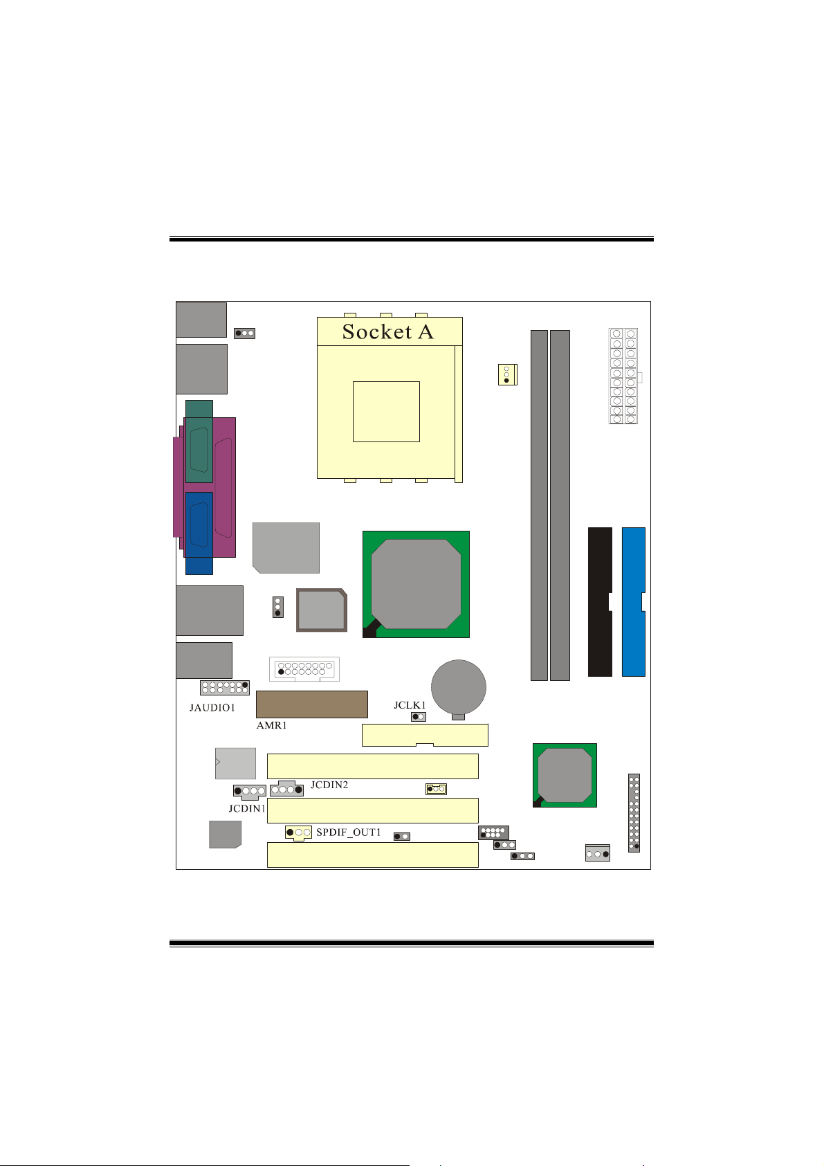
Layout of M7SUA
JKBMS1
1
JUSBV2
JUSB1
JCOM1
JPRNT1
CPU1
Winbond
JVGA1
JUSBLAN2
13
14
LAN
Phy
1
Codec
Phy
JAUDIO
I/O
JUSBV3
BIOS
1
JGAME1
216
1
1
2
1
PCI3
15
PCI1
1
※NOTE: ●represents the first pin.
SIS 740
1 2
1
PCI2
JCI1
1
BAT1
JWOL1
JUSB2
2
1
JCFAN1
FDD1
1
1
JCMOS1
1
10
9
JUSBV1
DDR1
DDR2
SIS 962L
JSFAN1
JATXPWR1
IDE1IDE2
SECONDARY IDE CONN.
PRIMARY IDE CONN.
JPANEL1
23
24
1
12
1
Page 4
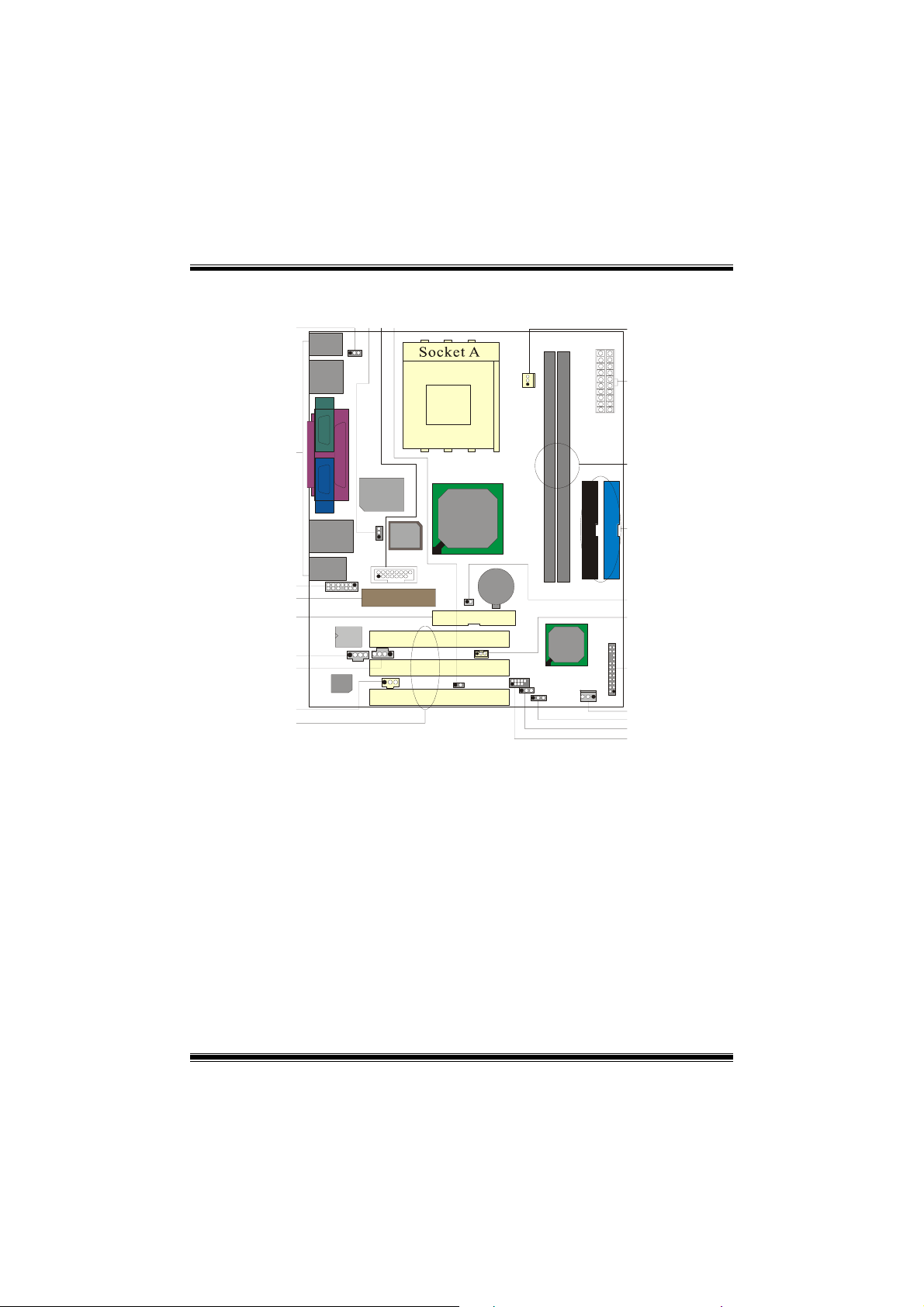
Component Index
W U
Codec
Phy
LAN
V
DDR1
Winbond
I/O
DDR2
SIS 740
BIOS
BAT1
Phy
SIS 962L
SECONDARY IDE CONN.
PRIMARY IDE CONN.
T
S
R
Q
P
O
N
M
L
K
J
A
B
A. 5V/5VSB Selection for USB K. 5V/5VSB Selection for USB
(JUSBV2) (JUSBV1)
B. Back Panel Connectors L. Clear CMOS Jumper (JCMOS1)
C. Front Audio Header (JAUDIO1) M. System Fan Header (JSFAN1)
D. Audio Modem Riser (AMR1) N. Front Panel Connector (JPANEL1)
(optional) O. Wake On LAN Header (JWOL1)
E. Floppy Disk Connector (FDD1) P. Frequency Selection (JCLK1)
F. CD-ROM Audio-In Header (JCDIN1) Q. Hard Disk Connectors (IDE1-2)
G. CD-ROM Audio-In Header (JCDIN2) R. DDR DIMM Modules (DDR1-2)
H. Digital Audio Connector S. ATX Power Connector (JATXPWR1)
(SPDIF_OUT1) T. CPU Fan Connector (JCFAN1)
I. Peripheral Component U. Case Open Connector (JCI1)
Interconnect Slot (PCI1-3) V. Game Header (JGAME1)
J. Front USB Header (JUSB2) W. 5V/5VSB Selection for USB (JUSBV3)
C
D
E
F
G
H
I
2
Page 5

English
M7SUA Features
A. Hardware
CPU
Provides Socket A.
Supports the single AMD® for AthlonTM (ThunderbirdTM )/ Athlon XPTM/ DuronTM
processors.
Front Side Bus at 200/ 266/ Fuzzy333 MHz.
Chipset
North Bridge: SIS 740.
South Bridge: SIS 962L
Main Memory
Supports up to 2 DDR devices.
Supports 200/ 266/ Fuzzy333 MHz (without ECC) DDR devices.
Maximum memory size of 2GB.
Super I/O
Chip: ITE IT8705.
Slots
Three 32-bit PCI bus master slots.
One AMR slot. (optional)
On Board IDE
Supports four IDE disk drives.
Supports PIO Mode 4, Bride Mode and Ultra DMA 33/66/100/133 Bus Master
Mode.
On Board AC’97 Sound Codec
Chip: VT1612A. (only for AC97 2.2)
Compliant with AC’97 specification.
AC97 2.2 interface.
Supports 2 audio output channels.
On Board Peripherals
1 floppy port supports 2 FDDs with 360K, 720K, 1.2M, 1.44M and 2.88Mbytes.
1 serial port.
1 VGA port.
1 parallel port. (SPP/EPP/ECP mode)
1 vertical audio port.
1 LAN port. (optional)
PS/2 mouse and PS/2 keyboard.
3
Page 6
6 USB2.0 ports. (front*2 + rear*4)
Front Side I/O Header
Front side audio header.
Front side USB headers.
Dimensions
Micro ATX Form Factor: 19.1 X 22.9cm (W X L)
B. BIOS & Software
BIOS
Award legal BIOS.
Supports APM1.2.
Supports ACPI.
Supports USB Function.
Software
Supports 9th TouchTM, FLASHER™ and StudioFun!
Offers the highest performance for Windows 98 SE, Windows 2000, Windows Me,
Windows XP, SCO UNIX etc.
TM
(optional)
Package Contents
HDD Cable X1
FDD Cable X1
User’s Manual X1
USB Cable X1 (optional)
Rear I/O Panel for ATX Case X1 (optional)
Fully Setup Driver CD X1
StudioFun! Application CD X1 (optional)
S/PDIF Out Cable X1 (optional)
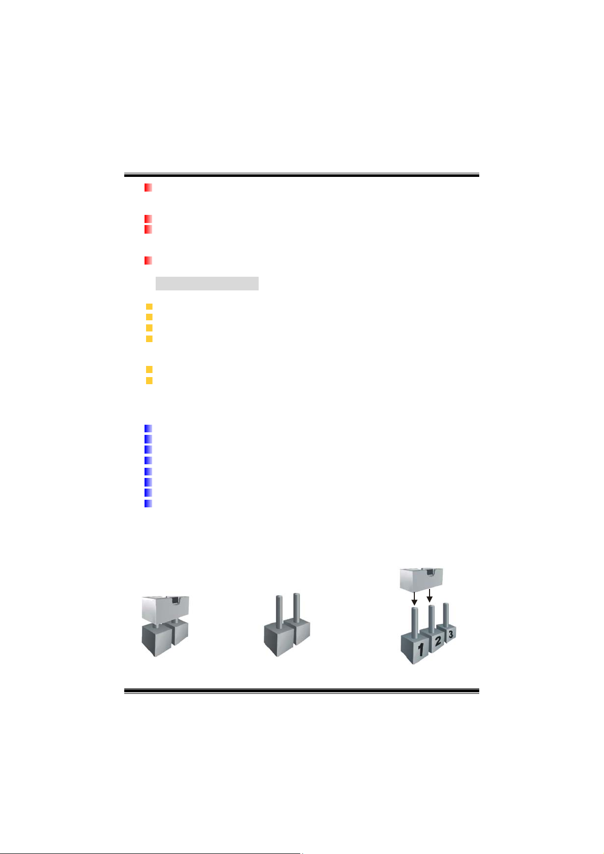
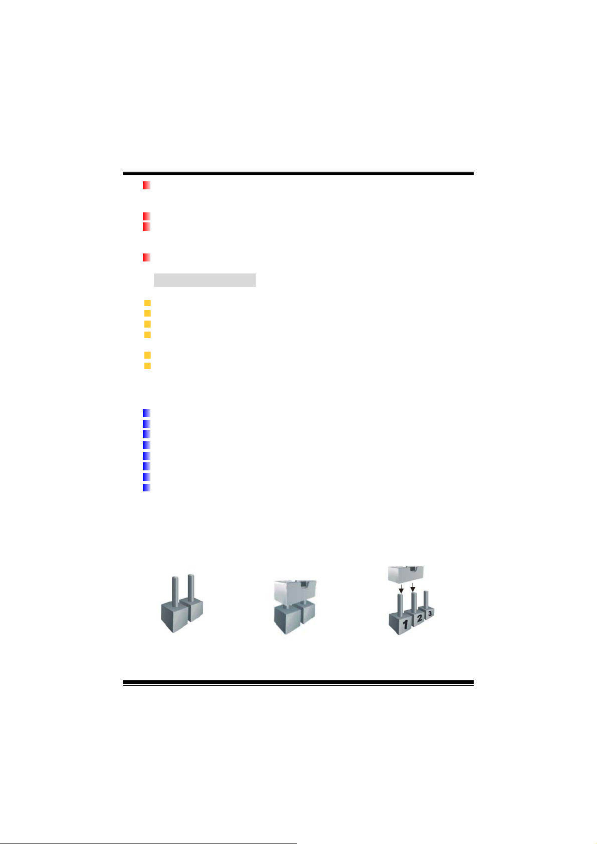
How to setup Jumper
The illustration shows how jumpers are setup. When the Jumper cap is placed on pins, the
jumper is “close”. If no jumper cap is placed on the pins, the jumper is ”open”. The
illustration shows a 3-pin jumper whose pin 1and 2 are “close” when jumper cap is placed
on these 2 pins.
Jumper close Jumper open Pin1-2 close
4
Page 7
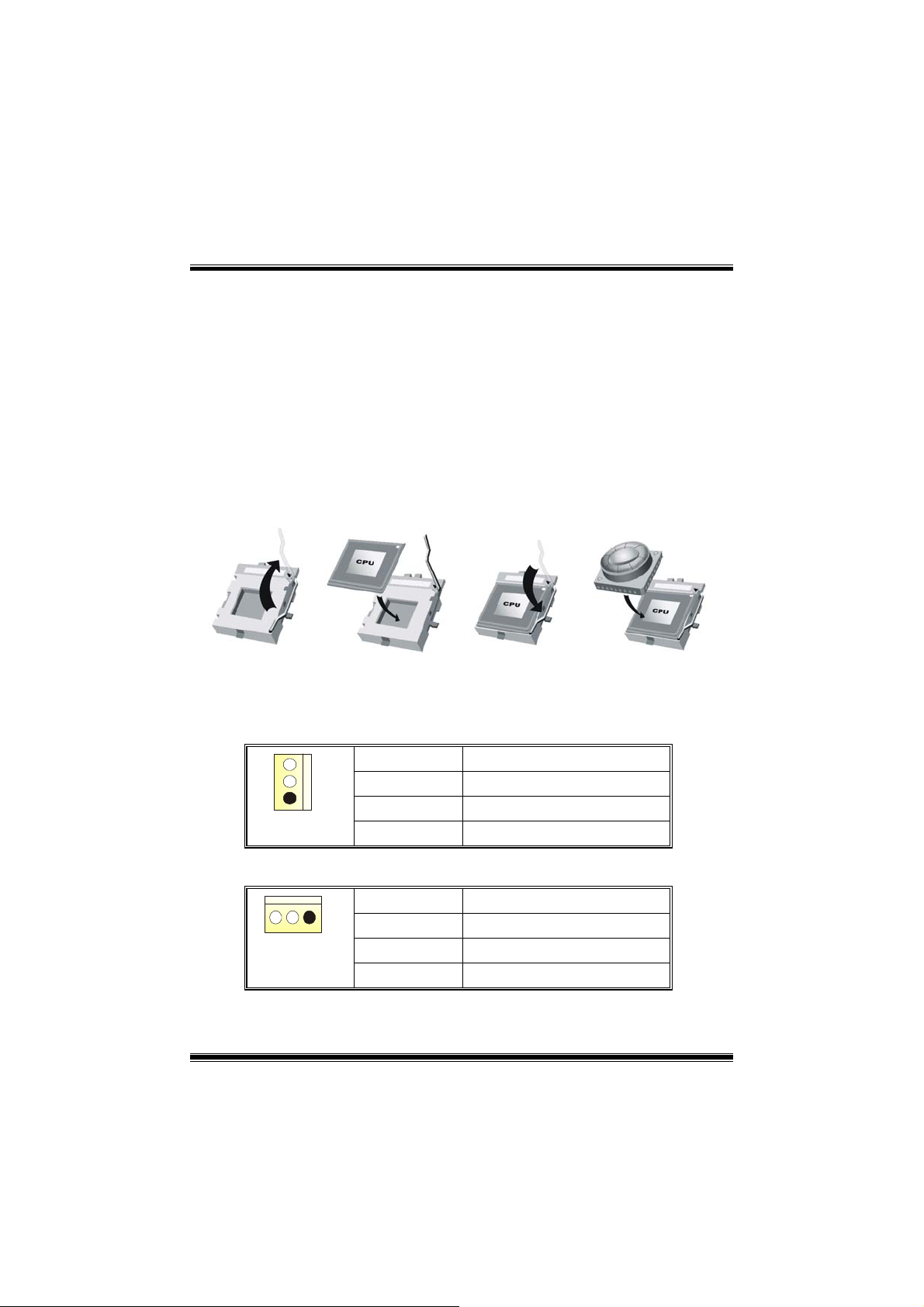
CPU Installation
Step1: Pull the lever sideways away from the socket and then raise the lever up to a
90-degree angle.
Step2: Look for the white dot/cut edge. The white dot/cut edge should point towards the
lever pivot. The CPU will fit only in the correct orientation.
Step3: Hold the CPU down firmly, and then close the lever.
Step4: Put the CPU fan on the CPU and buckle it. Connect the CPU fan power cable to
the JCFAN1. This completes the installation.
Step1 Step2 Step3 Step4
CPU Fan Headers: JCFAN1
3
1
JCFAN1
Pin No. Assignment
System Fan Headers: JSFAN1
1
JSFAN1
Pin No. Assignment
1
2
3
1
2
3
FAN R.P.M. Sense
FAN R.P.M. Sense
5
Ground
+12V
Ground
+12V
Page 8
DDR DIMM Modules: DDR1/ DDR2
DRAM Access Time: 2.5V Unbuffered DDR 200/ 266/ Fuzzy333 MHz Type required.
DRAM Type: 64MB/ 128MB/ 256MB/ 512MB/ 1GB DIMM Module (184 pin)
Total Memory Size with Unbuffered DIMMs
DIMM Socket
Location
DDR1 64MB/128MB/256MB/512MB/1GB
DDR2 64MB/128MB/256MB/512MB/1GB
DDR Module Total Memory
Size (MB)
*1
*1
***Only for reference***
Max is
2GB
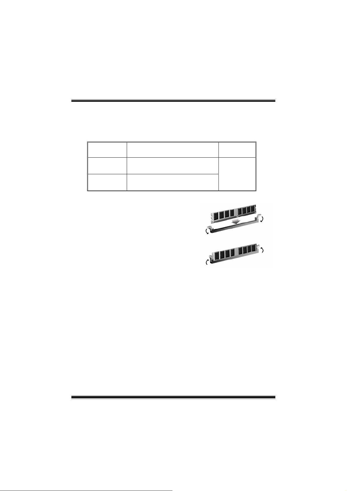
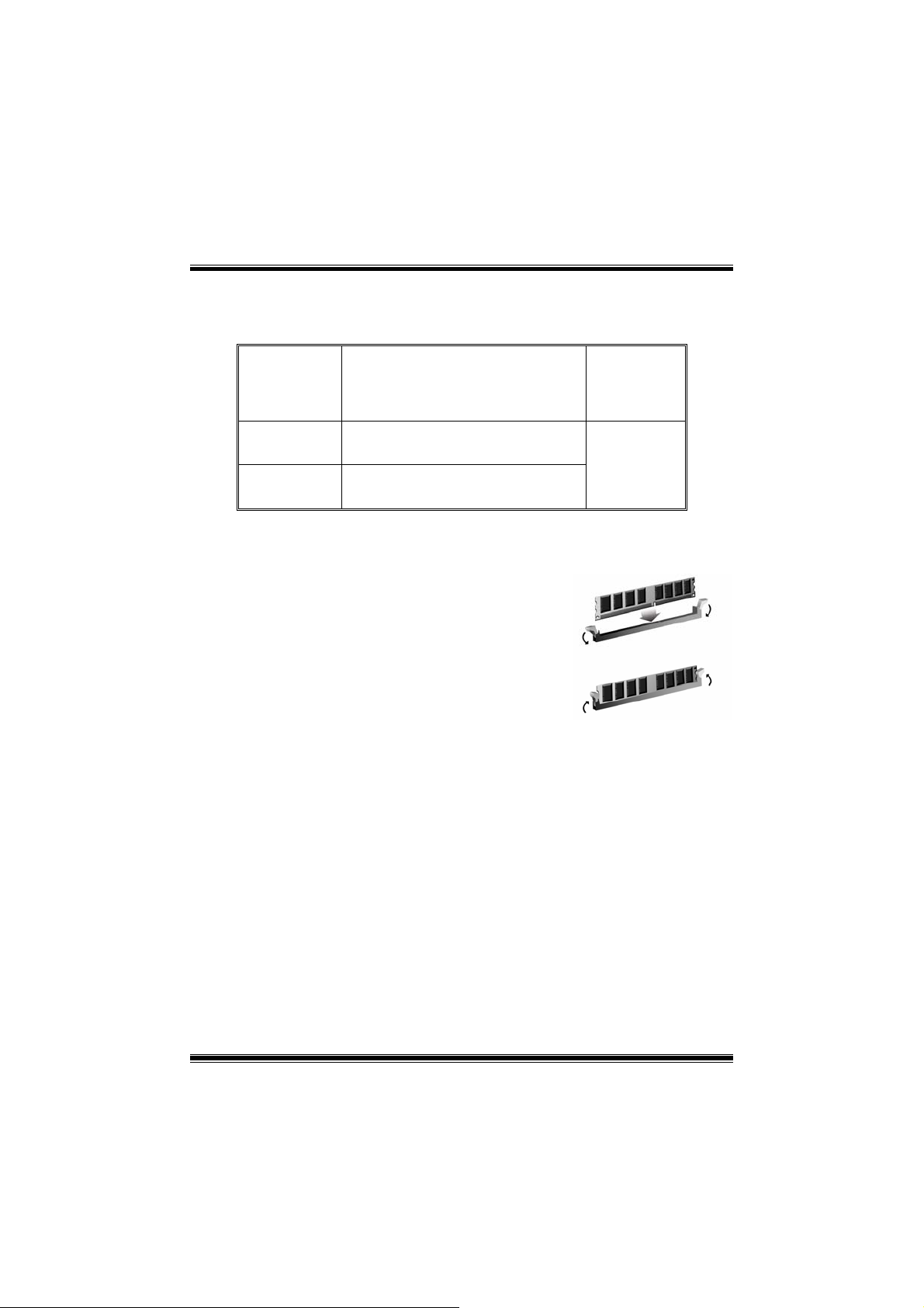
Installing DDR Module
1. Unlock a DIMM slot by pressing the
retaining clips outward. Align a DIMM on
the slot such that the notch on the DIMM
matches the break on the slot.
2. Insert the DIMM firmly and vertically into
the slot until the retaining chip snap back in
place and the Dimm is properly seated.
Jumpers, Headers, Connectors & Slots
Floppy Disk Connector: FDD1
The motherboard provides a standard floppy disk connector that supports 360K,
720K, 1.2M, 1.44M and 2.88M floppy disk types. This connector supports the
provided floppy drive ribbon cables.
Hard Disk Connectors: IDE1/ IDE2
The motherboard has a 32-bit Enhanced PCI IDE Controller that provides PIO
Mode 0~4, Bus Master, and Ultra DMA 33/ 66/ 100/ 133 functionality. It has two
HDD connectors IDE1 (primary) and IDE2 (secondary).
The IDE connectors can connect a master and a slave drive, so you can connect
up to four hard disk drives. The first hard drive should always be connected to
IDE1.
Peripheral Component Interconnect Slots: PCI1-3
This motherboard is equipped with 3 standard PCI slots. PCI stands for Peripheral
Component Interconnect, and it is a bus standard for expansion cards. This PCI
6
Page 9
0
slot is designated as 32 bits.
Audio Modem Riser Slot: AMR1 (optional)
(Only support slave card)
The AMR specification is an open Industry Standard Architecture and that defines
a hardware scalable riser card interface, which supports audio and modem only.
Front Panel Connector: JPANEL1
SLP
JPANEL1
Pin Assignment Function Pin Assignment Function
1
3
5
7
9
HDD LED (+)
11
HDD LED (-)
13
15
Reset Control
17
19
21
23
2
1
+5V
NA
NA
Speaker
Ground
NA
NA
+5V
IRTX
PWR_LED
(+) (-)(+)
SPK
Speaker
Connector
Hard Drive
LED
Reset
Button
IrDA
Connector
(+) (-)
HLED
RST
2
4
6
8
10
12
14
16
18
20
22
24
IRON/OFF
24
23
IR
Sleep Control
Ground
NA NA
Power LED (+)
Power LED (+)
Power LED (-)
Power Button
Ground
KEY
KEY
Ground
IRRX
Sleep
Button
POWER
LED
Power-on
Button
IrDA
Connector
Front USB Header: JUSB2
2
1
JUSB2
Pin Assignment Pin Assignment
1
1
3
9
5
7
9
+5V(fused)
USBP3-
USBP3+
Ground
KEY
2
4
6
8
10
+5V(fused)
USBP2-
USBP2+
Ground
NA
7
Page 10
Wake On LAN Header: JWOL1
13
JWOL1
Pin Assignment
1
2
3
+5V_SB
Ground
Wake up
Power Connectors: JATXPWR1
PIN Assignment PIN Assignment
1 +3.3V 11 +3.3V
2 +3.3V 12 -12V
3 Ground 13 Ground
4 +5V 14 PS_ON
5 Ground 15 Ground
6 +5V 16 Ground
7 Ground 17 Ground
8 PW_OK 18 -5V
9 +5V_SB 19 +5V
10 +12V 20 +5V
10
1
JATXPWR1
20
11
5V/ 5VSB Selection for USB (optional): JUSBV1/ JUSBV2/
JUSBV3
JUSBV1/ JUSBV2/
JUSBV3
Assignment Description
1 3
Pin 1-2 close
1 3
Pin 2-3 close
+5V
+5V_SB JUSBV1: JUSB2 port powered with
JUSBV1: 5V for JUSB2 port
JUSBV2: 5V for JUSB1 port
JUSBV3: 5V for JUSBLAN2 port
standby voltage 5V
JUSBV2: JUSB1 port powered with
standby voltage 5V
JUSBV3: JUSBLAN2 port powered with
standby voltage 5V
8
Page 11
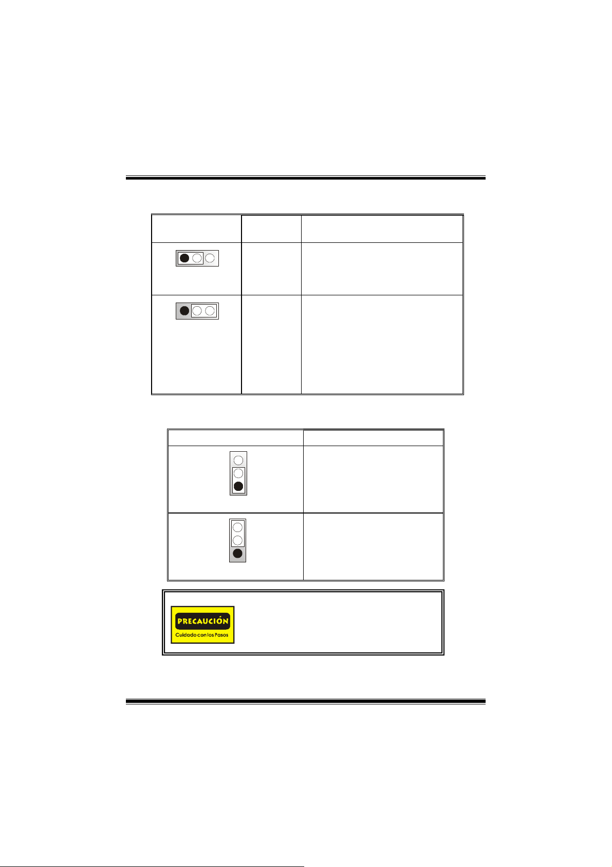
Clear CMOS Jumper: JCMOS1
JCMOS1 Assignment
3
1
Pin 1-2 Close
3
1
Pin 2-3 Close
The following procedures are for resetting the
BIOS password. It is important to follow these
instructions closely.
※ Clear CMOS Procedures:
1. Remove AC power line.
2. Set the jumper to “Pin 2-3 close”.
3. Wait for five seconds.
4. Set the jumper to “Pin 1-2 close”.
5. Power on AC.
6. Reset your desired password or clear the CMOS data.
Case Open Connector: JCI1 (optional)
Pin
Normal Operation (default)
Clear CMOS Data
Assignment
1
JCI1
1
2
Case Open Signal
9
Ground
Page 12

Front Panel Audio Header: JAUDIO1
2
4
6
8
12
14
1
2
Audio Power
RT Line Out
LFT Line In
13
14
JAUDIO1
Pin Assignment Pin Assignment
1
3
5
7
9 LFT Line Out 10 LFT Line Out
11
13
Mic In
Mic Power
RT Line Out
Reserved
RT Line In
LFT Line In
Digital Audio Connector: SPDIF_OUT1
Pin Assignment
1
2
3
SPDIF_OUT
1
3
SPDIF_OUT1
GAME Header: JGAME1 (optional)
216
Ground
Key
RT Line In
+5V
Ground
1
JGAME1
Pin Assignment Pin Assignment
1
3
5
7
9
11
13
15
+5V
GPSB1
GPX2
MIDI-OUT
GPY2
GPSB2
MIDI-IN
NA
10
15
2
4
6
8
10
12
14
16
+5V
GPSA1
GPX1
Ground
Ground
GPY1
GPSA2
+5V
Page 13

CD-ROM Audio-In Header: JCDIN1/ JCDIN2
1
JCDIN1/ 2
Pin Assignment
1
2
3
4
Left Channel Input
Ground
Ground
Right Channel Input
Frequency Selection: JCLK1 (optional)
CPU Clock PIN 1-2
100MHz
133MHz
OPEN
CLOSE
Note: Frequency Selection for Fuzzy333 MHz is selected throught BIOS
setup.
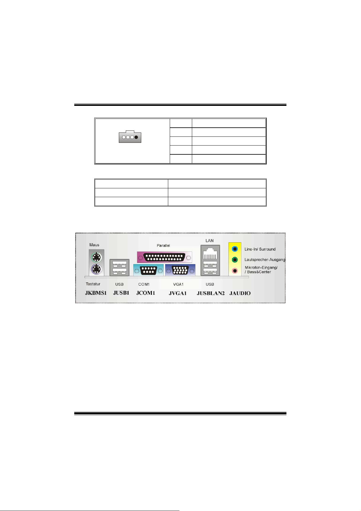
Back Panel Connectors
Mouse
Keyboard
JKBMS1
USB
JUSB1
Parallel
1
1 3
COM1
JCOM1
3
JVGA1
11
LAN
USB
JUSBLAN2
Line In/ Sur round
Speaker Out
Mic In/ Bass&Center
JAUDIO
Page 14

Español
Características del M7SUA
A. Hardware
CPU
Proporciona Socket A.
Soporta single AMD® para procesadores AthlonTM (ThunderbirdTM )/ Athlon XPTM/
TM
Duron
Front Side Bus 200/ 266/ Fuzzy333 MHz.
Chipset
North Bridge: SIS 740.
South Bridge: SIS 962L
Memoria Principal
Soporta hasta up to 2 DDR devices.
Soporta dispositivos DDR 200/ 266/ Fuzzy333 MHz (sin ECC).
Tamaño de memoria máxima 2GB.
Super I/O
Chip: ITE IT8705.
Ranuras
Tres PCI bus master de 32-bit.
Una ranura AMR. (opcional)
IDE Onboard
Soporta cuatro discos duros IDE.
Soporta modo PIO 4, modo Bride y Ultra DMA 33/66/100/133 Bus modo Master.
AC’97 Sound Codec Onboard
Chip: VT1612A. (solamente para AC97 2.2)
Conforma con la especificación AC’97.
Interface AC97 2.2.
Soporta 2 canales de salida de audio.
Periféricos Onboard
1 puerto de disquetera que soporta 2 FDDs con 360K, 720K, 1.2M, 1.44M y
1 puerto serie.
1 puerto VGA.
1 puerto paralelo. (modo SPP/EPP/ECP)
1 puerto de audio vertical.
1 puerto LAN. (opcional)
Ratón PS/2 y teclado PS/2.
.
2.88Mbytes.
12
Page 15
6 puertos USB2.0 (frontal*2 + traseros*4)
Cabezal del lado frontal I/O
Cabezal frontal de audio.
Cabezal frontal USB.
Dimensiones
Factor de Forma Micro ATX: 19.1 X 22.9 cm (W X L)
B. BIOS & Software
BIOS
Award legal BIOS.
APM1.2.
ACPI.
Función USB.
Software
Soporta 9th Touch
Ofrece el más alto funcionamiento para Windows 98 SE, Windows 2000,
Windows Me, Windows XP, SCO UNIX etc.
TM
, FlasheTM and StudioFun!
TM
(optional).
Contenido del Paquete
Cable HDD X1
Cable FDD X1
Manual del Usuario X1
Cable USB X1 (opcional)
Panel Trasero I/O para carcasa ATX X1 (opcional)
Configuración completa del Driver CD X1
Aplicación del CD StudioFun! X1 (opcional)
Cable S/PDIF Out X1 (opcional)
Cómo instalar un Puente
La ilustración muestra cómo instalar un puente. Cuando el Jumper Cap está ubicado en
los contactos, el puente está en “close”. Si no hay Jumper Cap ubicado en los contactos,
el puente está en ”open”. La siguiente ilustración muestra un contacto 3 en el que los
contactos 1y 2 están “close” cuando el Jumper Cap está ubicado en los dos contactos.
Puente open Puente close Contacto 1-2 close
13
Page 16

Instalación del CPU
Paso 1: Empuje la palanca hacia afuera del socket y levante la palanca hasta un ángulo de
90 grados.
Paso 2: Fíjese por el punto blanco o márgen cortado. El punto blanco o márgen cortado
debería apuntar hacia el pivote de la palanca. La CPU solamente se fijará en una
sola correcta orientación.
Paso 3: Tome el CPU firmemente hacia abajo, y cierre la palanca para completar la
instalación.
Paso 4: Ponga el ventilador de la CPU en el CPU y asegúrelo. Conecte el cable de
corriente del ventilador de la CPU al JCFAN1. Ésto completa la instalación.
paso 1 paso 2 paso 3 paso 4
Cabezales de Ventilación de la CPU: JCFAN1
3
1
JCFAN1
Contacto No. Asignación
1
2
3
FAN R.P.M. Sense
Tierra
+12V
System Fan Headers: JSFAN1
Contacto No. Asignación
JSFAN1
1
1
2
3
Tierra
+12V
FAN R.P.M. Sense
Módulos DDR DIMM: DDR1/ DDR2
DRAM Tiempo de Acceso: 2.5V Unbuffered DDR 200/ 266/ Fuzzy333 MHz Tipo
14
Page 17
requerido.
DRAM Tipo: 64MB/ 128MB/ 256MB/ 512MB/ 1GB Módulos DIMM (contactos 184)
Total del Tamaño de Memoria con Unbuffered DIMMs
Localización
del DIMM
Socket
Módulo DDR Total del
Tamaño de
Memoria
(MB)
DDR1 64MB/128MB/256MB/512MB/1GB
*1
DDR2 64MB/128MB/256MB/512MB/1GB
*1
***Solamente para referencia***
Máxima
2GB
Instalación del Módulo DDR
1. Abra una ranura de DIMM presionando el clip
de retención hacia afuera. Aliñe el DIMM en la
ranura tales que la muesca en el DIMM encaje
en la cumbrera de la ranura.
2. Inserte el DIMM verticalmente y firmemente en
la ranura hasta que el clip de retención vuelva a
su posición original y el DIMM esté
correctamente colocado.
Puentes, Cabezales, Conectores y Ranuras
Conector para Disquetera: FDD1
La placa madre proporciona un conector estándar para disquete que soporta
disquetera de 360K, 720K, 1.2M, 1.44M y 2.88M. Éste conector utiliza cables
proporcionados por el disquete.
Conectores de Disco Duro: IDE1/ IDE2
La placa madre tiene un controlador de 32-bit PCI IDE que proporciona Modo PIO
0~5, Bus Master, y funcionalidad Ultra DMA 33/ 66/ 100. Tiene dos conectores
HDD: IDE1 (primario) y IDE2 (secundario).
Los conectores IDE puede conectar a un disco master y uno esclavo, así puede
conectar hasta cuatro discos duros. El primer disco duro debe estar siempre
conectado al IDE1.
Ranuras de Interconexión del Componente Periférico: PCI1-3
Ésta placa madre está equipada con 3 ranuras estándar PCI. PCI es la sigla para
15
Page 18

Interconexión del Componente Periférico, y es un bus estándar para tarjetas de
expansión. Ésta ranura PCI está diseñado con 32 bits.
Ranura Audio Módem Riser: AMR1 (opcional)
(Solamente soporta tarjeta esclava)
AMR es una industria estándar de arquitectura abierta en el que define interface
de tarjeta hardware escalable soportando solamente audio y módem.
Conector del Panel Frontal: JPANEL1
PWR_LED
(+) (-)(+)
SPK
Conector
del
Altavoz
LED del
Disco Duro
Botón
de Reinicio
(+) (-)
HLED
JPANEL1
Contacto
1
3
5
7
9
11
13
15
17
19
21
23
SLP
2
1
Asignación Función Con-
+5V
NA
NA
Altavoz
HDD LED (+)
HDD LED (-)
Tierra
Control de
Reinicio
NA
NA
+5V
IRTX
Conector IrDA
Cabezal Frontal USB: JUSB2
Contac
tos
Asignación
RST
tacto
2
4
6
8
Corriente LED(+)
10
Corriente LED(+)
12
Corriente LED (-)
14
16
18
20
22
24
IRON/OFF
24
23
IR
Asignación Función
Control de
Suspension
Tierra
NA NA
Botón de
Encendido
Tierra
KEY
KEY
Tierra
IRRX
Contac
tos
Asignación
Botón
de Suspensión
LED
del Corriente
Botón
de Encendido
Conector IrDA
16
Page 19

0
2
1
JUSB2
1
1
3
9
5
7
9
+5V(fused)
USBP3-
USBP3+
Tierra
KEY
Cabezal Wake On LAN: JWOL1
13
JWOL1
Contactos Asignación
1
2 Tierra
3
Conector de Corriente: JATXPWR1
10
1
JATXPWR1
20
11
Contac
tos
1 +3.3V 11 +3.3V
2 +3.3V 12 -12V
3 Tierra 13 Tierra
4 +5V 14 PS_ON
5 Tierra 15 Tierra
6 +5V 16 Tierra
7 Tierra 17 Tierra
8 PW_OK 18 -5V
9 +5V_SB 19 +5V
10 +12V 20 +5V
Asignación Contac
2
4
6
8
10
tos
+5V(fused)
USBP2-
USBP2+
Tierra
NA
+5V_SB
Wake up
Asignación
17
Page 20
5V/ 5VSB Selección para USB (opcional): JUSBV1/ JUSBV2/
JUSBV3
JUSBV1/ JUSBV2/
JUSBV3
Asignación Descripción
1 3
Contactos 1-2 close
1 3
Contactos 2-3 close
+5V
+5V_SB JUSBV1: puerto JUSB2 voltaje standby
Puente de Borrar CMOS: JCMOS1
※ Procesos para Borrar CMOS:
1. Quite el cable de corriente del AC.
2. Fijar el puente en el “contacto 2-3 close”.
JCMOS1 Assignment
3
1
Contacto 1-2 Close
3
1
Contactos 2-3 Close
Los siguientes procesos son para reiniciar la
contrasena del BIOS. Es importante que siga los
~
siguientes pasos cuidadosamente.
JUSBV1: 5V para puerto JUSB2
JUSBV2: 5V para puerto JUSB1
JUSBV3: 5V para puerto JUSBLAN2
de 5V
JUSBV2: puerto JUSB1 voltaje standby
de 5V
JUSBV3: puerto JUSBLAN2 voltaje
standby de 5V
Operación Normal (default)
Borrar Datos CMOS
18
Page 21

3. Espere 5 segundos.
4. Fijar el Puente en el “contacto 1-2 close”.
5. Encienda AC.
6. Reconfigure la contraseña deseada o borre datos CMOS.
Conector de la Carcasa Abierta: JCI1 (opcional)
Contactos
Asignación
1
JCI1
1
2
Señal de la Carcasa Abierta
Tierra
Cabezal del Panel de Audio Frontal: JAUDIO1
tos
2
4
6
8
10
12
14
1
2
Asignación
Corriente de Audio
Salida de Línea RT
Salida de Línea LFT
Entrada de Línea RT
Entrada de Línea LFT
Contac-
tos
1
3
5
7
9
11
13
13
14
JAUDIO1
Asignación Contac-
Entrada del Mic
Corriente del Mic
Salida de Línea RT
Reservado
Salida de Línea LFT
Entrada de Línea RT
Entrada de Línea LFT
Conector Digital de Audio: SPDIF_OUT1
1
SPDIF_OUT1
3
Contactos Asignación
1
2
3
SPDIF_OUT
Tierra
Key
+5V
Tierra
19
Page 22

Cabezal de Juego: JGAME1 (opcional)
216
Contac-
tos
1
3
5
7
9
11
13
15
1
JGAME1
Asignación Contac-
+5V
GPSB1
GPX2
MIDI-OUT
GPY2
GPSB2
MIDI-IN
NA
tos
2
4
6
8
10
12
14
16
15
Asignación
+5V
GPSA1
GPX1
Tierra
Tierra
GPY1
GPSA2
+5V
Cabezal de Entrada de Audio CD-ROM: JCDIN1/ JCDIN2
JCDIN1/ 2
Contac-
tos
1
1
2
3
4
Entrada del Canal Izquierdo
Asignación
Tierra
Tierra
Entrada del Canal Derecho
Selección de Frecuencia: JCLK1 (opcional)
CPU Clock Contacto 1-2
100MHz
133MHz
Nota: Selección de Frecuencia para Fuzzy333 MHz se selecciona por medio
de la Configuración del BIOS.
OPEN
CLOSE
20
Page 23

Back Panel Connectors
Mouse
Keyboard
JKBMS1
USB
JUSB1
Parallel
1
1 3
COM1
JCOM1
3
JVGA1
LAN
USB
JUSBLAN2
Line In/ Sur round
Speaker Out
Mic In/ Bass&Center
JAUDIO
21
Page 24

Deutsch
Spezifikationen von M7SUA
A. Hardware
CPU
Unterstützung für Sockel A.
Unterstütz den Einzel AMD® für Athlon
Prozessor.
FSB mit 200/266/Fuzzy333 MHz.
Chipsatz
Northbridge: SIS 740.
Southbridge: .SIS 962L.
Hauptspeicher
Unterstützung für 2 DDR Geräte.
Unterstützung für 200/266/Fuzzy333 MHz(ohne ECC) DDR Geräte.
Die maximale Speichergröße ist 2GB.
Super I/O
Chip: ITE IT8705.
Slots
Drei 32-Bit PCI-Bus-Slots.
Ein AMR-Slot.
Onboard-IDE
Unterstützung für vier IDE Diskettenlaufwerke.
Unterstützung für PIO Modus 4, Bride Modus und Ultra DMA 33/66/100/133 Bus
Master Modus.
Onboard AC’97 Sound Codec
Chip: VT1612A. (AC97 2.2 nur)
Entspricht die Spezifikation von AC’97.
AC97 2.2 Interface.
Unterstützung für 2-Kanal Audio Ausgang.
Onboard-Peripheriegeräte
1 Floppy-Port mit Unterstützung für 2 Diskettenlaufwerke.(360KB, 720KB, 1.2MB,
1.44MB und 2.88MB)
1 serielle VGA-Schnittstelle.
1 VGA-Schnittstelle
1 parallele Schnittstelle. (SPP/EPP/ECP-Modus)
1 vertikales Audio-Port.
1 LAN-Port. (optional)
TM
(Thunderbird
TM
)/ Athlon XP
TM
/ Duron
TM
22
Page 25

Unterstützung für PS/2-Maus und PS/2-Tastatur.
6 USB2.0-Ports. (Vorderseite x 4 + Rückwand x 2)
Vorderseite-I/O-Header
Vorderseite Audio Header. (Front side audio header)
Vorderseite USB Header. (Front side USB header)
Abmessungen
Mikro ATX Form-Factor: 19.1 X 22.9cm (W X L)
B. BIOS & Software
BIOS
Award legal Bios.
Unterstützung für APM1.2.
Unterstützung für ACPI.
Unterstützung für USB Funktion.
Software
Unterstützung 9th TouchTM, FLASHER™ und StudioFun! ™.
Unterstützung für die am meisten verbreiteten Betriebsysteme wie Windows 98SE,
Windows 2000, Windows ME, Windows XP and SCO UNIX usw.
Verpackungsinhalt
HDD Kable X1
FDD Kable X1
Benutzer Handbuch X1
USB Kable X1 (optional)
I/O-Rückwand für ATX Gehäuse X1 (optional)
Treiber CD für Installation X 1
StudioFun! Application CD x 1 (optional)
S/PDIF Ausgang Kable X1 (optional)
Einstellung der Jumper
Die Abbildung verdeutlicht, wie Jumper eingestellt werden. Pins werden durch die
Jumper-Kappe verdeckt, ist der Jumper ”geschlossen”. Keine Pins werden durch die
Jumper-Kappe verdeckt, ist der Jumper “geöffnet”. Die Abbiildung zeigt einen 3-Pin
Jumper dessen Pin1 und Pin2 ”geschlossen“ sind, bzw. es befindet sich eine
Jumper-Kappe auf diesen beiden Pins.
Jumper geschlossen Jumper geöffnet Pin1-2 geschlossen
23
Page 26

Installation der CPU
Schritt 1: Ziehen Sie den Hebel seitlich vom Sockel weg. Heben Sie den Hebel dann
in 90-Grad-Winkel nach oben.
Schritt 2: Suchen Sie nach der scharfen Kante, die auf Drehpunkt des Hebels
weisen muss. Die CPU passt nur, wenn sie richtig ausgerichtet ist.
Schritt 3: Drücken Sie die CPU fest in den Sockel und schließen Sie den Hebel.
Schritt 4: Stecken Sie Ihren CPU-Lüfter auf die CPU. Schließen Sie die Stromversorgungsstecker
für CPU-Lüfter an JCFAN1 an. Dann beenden Sie die Installation.
Schritt 1 Schritt 2 Schritt 3 Schritt 4
CPU-Lüfter Headers: JCFAN1
Pin
1
1
JCFAN1
2
3
System-Lüfter Headers: JSFAN1
1
JSFAN1
Pin
1
2
3
Beschreibung
Masse
+12V
Lüfter R.P.M. Rate Sensor
Beschreibung
Masse
+12V
Lüfter R.P.M. Rate Sensor
24
Page 27

DDR-DIMM-Modules: DDR1/ DDR2
DRAM-Zugriffszeit: 2.5V nicht registrierter DDR 200/266/Fuzzy333 MHz Typ
erforderlich.
DRAM-Typen: 64MB/ 128MB/ 256MB/ 512MB/ 1GB DIMM-Module (184-Pin)
Gesamt Speichergröße von nicht registrierter DIMMs
DIMM-Sockel
Standort
DDR1 64MB/128MB/256MB/512MB/1GB
DDR2 64MB/128MB/256MB/512MB/1GB
DDR-Modul Speichergröße
(MB)
*1
*1
**Nur als Referenz***
maximal
2GB
Installation von DDR-Modul
1. Öffnen Sie einen DIMM-Slots, indem Sie
die seitlich Chips nach außen drücken.
Richten Sie das DIMM-Modul so über dem
Slot aus, dass das Modul mit der Kerbe in
den Slot passt.
2. Drücken Sie das DIMM-Modul in den Slot,
bis die seitlichen Clips zuschnappen und
das Modul fest sitzt.
Jumpers, Headers, Anschlüsse & Slots
Diskettenanschluss: FDD1
Das Motherboard enthält einen standardmäßigen Diskettenanschluss, der 360K-,
720K-, 1.2M-, 1.44M- und 2.88M-Disketten unterstützt. Dieser Anschluss
unterstützt die mitgelieferte Bandkabel des Diskettenlaufwerks.
Festplattenanschlüsse: IDE1 und IDE2
Das Mainboard hat einen 32-Bit Enhanced PCI IDE-Controller, der die Modi
PIO0~4, Bus Master sowie die Ultra DMA/33/66/100/133- Funktion zur Verfügung
stellt. Dieser ist mit zweii HDD-Anschlüssen versehen IDE1 (primär) und IDE2
(sekundär).
Die IDE-Anschlüsse können eine Master- und eine Slave-Festplatte verbinden, so
dass bis zu 4 Festplatten angeschlossen werden können. Die erste Festplatte
sollte immer an IDE1 angeschlossen werden.
Peripheral Component Interconnect Slots: PCI1-3
Dieses Motherboard ist mit 3 standardmäßigen PCI-Slots ausgestattet. PCI steht
25
Page 28

D
für Peripheral Component Interconnect und bezieht sich auf einem Busstandard für
Erweiterungskarten, der den älteren ISA-Busstandard in den meisten
Schnittstellen ersetzt hat. Dieser PCI-Slot ist für 32 bits vorgesehen.
Audio Modem Riser Slot: AMR1
(unterstützt nur Slave-Karte)
Die AMR-Spezifikation ist eine “offene Industrie-Standard-Architektur” und AMR
wird als ein skalierbares Riser-Karte-Interface von Hardware definiert , das nur
Modem und Soundfunktion unterstützt.
Anschlüsse für die Vorderseite: JPANEL1
SLP
JPANEL1
Pin Beschreibung Funktion Pin Beschreibung Funktion
1
3
5
7
Lautsprecher
9
HDD LED (+)
11
HDD LED (-)
13
15
Reset Control
17
19
21
23
*Schlüsse: Kein Pin.
2
1
+5V
Kein
Kein
Masse
Kein 18Schlüsse Kein Pin
Kein
+5V
IRTX
PWR_LED
(+) (-)(+)
SPK
(+) (-)
HLE
Lautsprecher
Anschluss
Festplatte
LED
Zurücksetzn-
Knopf
IrDA-
Anschluss
RST
2
4
6
8
10
12
14
16
20
22
24
IRON/OFF
24
23
IR
Sleep Control
Masse
Kein Kein
Power LED (+)
Power LED (+)
Power LED (-)
Power-Knopf
Masse
Schlüsse
Masse
IRRX
Schlafen-
Knopf
Power-
LED
Power-On
Knopf
IrDA
Anschluss
Front USB Header: JUSB2
2
1
10
9
Pin
1
3
5
Belegung
+5V(geschmelzt)
USBP4-
USBP4+
Pin
2
4
6
Belegung
+5V(geschmelzt)
USBP5-
USBP5+
26
Page 29

JUSB2
7
9
Masse
Schlüsse
8
10
Masse
Kein
Wake On LAN Header: JWOL1
Beschreibung
+5V_SB
Masse
Wake-up
1
JWOL1
Pin
1
2
3
Stromversorgungsanschluss: JATXPWER1
PIN Beschreibung PIN Beschreibung
1 +3.3V 11 +3.3V
2 +3.3V 12 -12V
3 Masse 13 Masse
4 +5V 14 PS_ON
5 Masse 15 Masse
6 +5V 16 Masse
7 Masse 17 Masse
8 PW_OK 18 -5V
9 +5V_SB 19 +5V
10 +12V 20 +5V
10
1
JATXPWR1
20
11
Auswahl von 5V/ 5V_SB für USB (optional): JUSBV1/ JUSBV2/
JUSBV3
JUSBV1/ JUSBV2/
JUSBV3
Beschreibung Funktion
1 3
Pin 1-2 geschlossen
1 3
Pin 2-3 geschlossen
+5V
+5V_SB
JUSBV1: 5V für JUSB2
JUSBV2: 5V für JUSB1
JUSBV3: 5V für JUSBLAN2
JUSBV1: 5V reserviert für JUSB2
JUSBV2 : 5V reserviert für JUSB1
JUSBV3: 5V reserviert für JUSBLAN2
27
Page 30

Jumper zum Löschen CMOS: JCMOS
JCMOS
3
1
Pin 1-2 geschlossen
3
1
Pin 2-3 geschlossen
Beschreibung
Normale Operation (Default)
CMOS-Daten Löschen
Die folgende Schritte leiten Sie, das Kennwort für
BIOS-System zurückzusetzen. Es ist wichtig, die
Anweisung zu folgen.
※ Prozeduren zum Löschen des CMOS:
1. Ausschalten Sie den AC-Netzstecker.
2. Lassen Sie Pin 2-3 von JCOMS1 geshclossen sein.
3. Bitte warten Sie 15 Sekunden.
4. Lassen Sie Pin 1-2 von JCOMS1 geshclossen sein.
5. Schließen Sie den AC-Netzstecker an.
6. Zurücksetzen Sie ihr gewünschtes Kennwort oder löschen Sie
die CMOS-Daten.
Anschluss für Gehäuse-Öffnen: JC1(optional)
Pin
Beschreibung
1
JC1
1
2
Gehäuse Öffnen Signal
Masse
28
Page 31

Front Panel Audio Header: JAUDIO1
2
1
JAUDIO1
Pin Beschreibung Pin Beschreibung
1
3
5
7
9 Link Line-Out 10 Link Line-Out
11
13
Mikrofon-Eingang
Mikrofon-Betriebsspannung
Recht Line-Out
Reserviert
Line-In RT
Line-In LFT
2
4
6
8
12
14
14
13
Masse
Audio-Spannung
Recht Line-Out
Schlüsse
Line-In RT
Line-In LFT
Digital Audio Anschluss: SPDIF_OUT1
1
SPDIF_OUT1
Pin Beschreibung
1
2
3
SPDIF_OUT
Game Header: JGAME1 (optional)
15
1
+5V
Masse
29
216
2
4
6
8
10
12
14
16
+5V
GPSA1
GPX1
Masse
Masse
GPY1
GPSA2
+5V
JGAME1
Pin Beschreibung Pin Beschreibung
1
3
5
7
9
11
13
15
+5V
GPSB1
GPX2
MIDI-OUT
GPY2
GPSB2
MIDI-IN
Kein
Page 32
CD-ROM Audio-In Header: JCDIN1/JCDIN2
Pin Beschreibung
1
2
3
4
Link-Kanal Eingabe
Masse
Masse
Recht-Kanal Eingabe
JCDIN1/2
1
Frequenz Auswahl: JCLK1 (optional)
CPU Takt PIN 1-2
100MHz
133MHz
Anmerkung: Frequenz Fuzzy333 MHz bitte wählen Sie Fuzzy333 in
„BIOS-Setup-Menü“
geöffnet
geschlossen
Anschlüsse für die Rückwand
30
Page 33

Trouble Shooting
PROBABLE SOLUTION
No power to the system at all Power light don’t
illuminate, fan inside power supply does not turn
on. Indicator light on keyboard does not turn on
PROBABLE SOLUTION
System inoperative. Keyboard lights are on,
power indicator lights are lit, hard drive is
spinning.
PROBABLE SOLUTION
System does not boot from hard disk drive, can
be booted from CD-ROM drive.
PROBABLE SOLUTION
System only boots from CD-ROM. Hard disk can
be read and applications can be used but
booting from hard disk is impossible.
* Make sure power cable is securely plugged in
* Replace cable
* Contact technical support
* Using even pressure on both ends of the
DIMM, press down firmly until the module
snaps into place.
* Check cable running from disk to disk controller
board. Make sure both ends are securely
plugged in; check the drive type in the
standard CMOS setup.
* Backing up the hard drive is extremely
important. All hard disks are capable of
breaking down at any time.
* Back up data and applications files. Reformat
the hard drive. Re-install applications and data
using backup disks.
PROBABLE SOLUTION
Screen message says “Invalid Configuration” or
“CMOS Failure.”
PROBABLE SOLUTION
Cannot boot system after installing second hard
drive.
* Review system’s equipment . Make sure
correct information is in setup.
* Set master/slave jumpers correctly.
* Run SETUP program and select correct drive
types. Call drive manufacturers for
compatibility with other drives.
31
Page 34

Solución de Problemas
CAUSA PROBABLE SOLUCIÓN
No hay corriente en el sistema. La luz de
corriente no ilumina, ventilador dentro de la
fuente de alimentación apagada. Indicador de
luz del teclado apagado.
CAUSA PROBABLE SOLUCIÓN
Sistema inoperativo. Luz del teclado encendido,
luz de indicador de corriente iluminado, disco
rígido está girando.
Sistema no arranca desde el disco rígido, puede
ser arrancado desde el CD-ROM drive.
Sistema solamente arranca desde el CD-ROM.
Disco rígido puede leer y aplicaciones pueden
ser usados pero el arranque desde el disco
rígido es imposible.
Mensaje de pantalla ”Invalid Configuration” o
“CMOS Failure.”
No puede arrancar después de instalar el
segundo disco rígido.
CAUSA PROBABLE SOLUCIÓN
CAUSA PROBABLE SOLUCIÓN
CAUSA PROBABLE SOLUCIÓN
CAUSA PROBABLE SOLUCIÓN
* Asegúrese que el cable de transmisión esté
seguramente enchufado.
* Reemplace el cable.
* Contacte ayuda técnica.
* Presione los dos extremos del DIMM, presione
para abajo firmemente hasta que el módulo
encaje en el lugar.
* Controle el cable de ejecución desde el disco
hasta el disco del controlador. Asegúrese de
que ambos lados estén enchufados con
seguridad; controle el tipo de disco en la
configuración estándar CMOS.
* Copiando el disco rígido es extremadamente
importante. Todos los discos rígidos son
capaces de dañarse en cualquier momento.
* Copie datos y documentos de aplicación.
Vuelva a formatear el disco rígido. Vuelva a
instalar las aplicaciones y datos usando el
disco de copiado.
* Revise el equipo del sistema. Asegúrese de
que la información configurada sea correcta.
* Fije correctamente el puente master/esclavo.
* Ejecute el programa SETUP y seleccione el
tipo de disco correcto. Llame a una
manufacturación del disco para compatibilidad
con otros discos.
32
Page 35

Problemlösung
MÖGLICHE URSACHE LÖSUNG
Das System hat keine Spannungsversorgung.
Die Stromanzeige leuchtet nicht, der Lüfter im
Inneren der Stromversorgung wird nicht
eingeschaltet. Tastaturleuchten sind nicht an.
MÖGLICHE URSACHE LÖSUNG
Das System funktioniert nicht. Die
Tastaturleuchten sind an, die Stromanzeige
leuchtet, die Festplatte dreht sich.
MÖGLICHE URSACHE LÖSUNG
Das System wird von der Festplatte nicht
hochgefahren, vom CD-ROM-Treiber aber ja.
MÖGLICHE URSACHE LÖSUNG
Das System wird nur von der CD-ROM
hochgefahren. Die Festplatte wird gelesen und
die Anwendungen sind funktionsfähig, aber es
ist nicht möglich, das System von der Festplatte
zu starten.
Auf dem Bildschirm erscheint die Meldung
“Ungültige Konfiguration” oder “CMOS Fehler.”
Das System kann nach der Installation einer
zweiten Festplatte nicht hochgefahren werden.
MÖGLICHE URSACHE LÖSUNG
MÖGLICHE URSACHE LÖSUNG
* Versichern Sie sich, dass das Stromkabel richtig
angebracht ist
* Ersetzen Sie das Stromkabel
* Wenden Sie sich an Ihre Kundendienststelle
* Drücken Sie das DIMM-Modul bei gleichem
Druck an beide Seiten, bis es einrastet.
* Überprüfen Sie das Kabel zwischen Festplatte
und Festplatten-Controller. Versichern Sie
sich, dass beide Enden richtig angebracht
sind; überprüfen Sie den Laufwerktyp in der
standardmäßigen CMOS-Einrichtung.
* Ein Backup der Festplatte ist sehr wichtig. Alle
Festplatten können irgendwann beschädigt
werden.
* Machen Sie eine Sicherungskopie von allen
Daten und Anwendungsdateien. Formatieren
Sie die Festplatte und reinstallieren Sie die
Anwendungen und Daten mit Hilfe von
Backup-Disks.
* Überprüfen Sie die Systemkomponenten und
versichern Sie sich, das diese richtig
eingerichtet sind.
* Setzen Sie die Master/Slave-Jumper richtig ein.
* Führen Sie das SETUP-Programm aus und
wählen Sie die richtigen Laufwerktypen.
Wenden Sie sich an den Laufwerkhersteller,
um die Kompatibilität mit anderen Laufwerken
zu überprüfen.
33
Page 36

05/16/2003
34
 Loading...