

Page 1

M
7
N
C
G
4
0
0
M
M
7
7
N
N
C
C
G
G
4
4
0
0
0
0
FCC Statement and Copyright
This equipment has been tested and found to comply with the limits of a
Class B digital device, pursuant to Part 15 of the FCC Rules. These limits
are designed to provide reasonable protection against harmful
interference in a residential installation. This equipment generates, uses
and can radiate radio frequency energy and, if not installed and used in
accordance with the instructions, may cause harmful interference to radio
communications. There is no guarantee that interference will not occur in
a particular installation.
The vendor makes no representations or warranties with respect to the
contents here of and specially disclaims any implied warranties of
merchantability or fitness for any purpose. Since our products are under
continual improvement, we reserve the right to make changes without
notice.
The material in this manual is the intellectual property of the vendor.
Further the vendor reserves the right to revise this publication and to
make changes to its contents without obligation to notify any party
beforehand. Duplication of this publication, in part or in whole, is not
allowed without first obtaining the vendor’s approval in writing. Even
thought we have taken every care in the preparation of this user’s manual,
no guarantee is given as to the correctness of its contents.
All the brand and product names are the property of their respective
owners.
i
Page 2

C
o
n
t
e
n
t
s
C
o
n
C
o
n
ENGLISH.................................................................................................1
M7NCG 400 Features .......... .. .... .. .. ... .. .. .. .. .... .. .. .. .. .. ... .... .. .. .. .. .. .. .. .... ... .. .. .. .. .. .... .. .. .. .. .. ... .. .... .1
Package contents................................................... ..............................................................2
Layout of M7NCG 400.......................................................................................................... 3
CPU Installation ....................................................................................................................4
CPU/ System Fan Headers: JCFAN1/ JSFAN1/ JNFAN1.. ...............................................4
DDR DIMM Modules: DIMMB1/DIMMB2/ DIMMA1... .. .. .. .. .. .. .... .. .. ... .. .. .. .. .. .. .. .... .. .. ... .. .. .. .. .5
How to install a DIMM Module.................... ............. ............ ............. ............ ............. .........5
Jumpers, Headers, Connectors & Slots.......................................................... .................. 6
t
e
n
t
s
t
e
n
t
s
ESPAÑOL..... ... ......................................................................................13
Características del M7NCG 400..................................... ...................................................13
Contenido del Paquete......................................................................................................14
Disposición del M7NCG 400.......................................................................................... ... 15
Instalación de la CPU.........................................................................................................16
Instalación de la CPU.........................................................................................................16
Módulos DDR DIMM: DIMMB1/DIMMB2/ DIMMA1................... .. ..... .. .. .. .. .. .. .. .. .... .. ... .. .. .. .17
Conectores, Cabezales, Puentes y Ranuras ..................................................................18
DEUTSCH..............................................................................................25
M7NCG 400 Features .......... .. .... .. .. ... .. .. .. .. .... .. .. .. .. .. ... .... .. .. .. .. .. .. .. .... ... .. .. .. .. .. .... .. .. .. .. .. ... .. ...25
Verpackungsinhalt......................................................... .....................................................26
Layout des M7NCG 400.... .. .... .. .. .. ... .. .. .. .. .... .. .. .. .. .. ... .. .. .... .. .. .. .. .. .. .. .. ..... .. .. .. .. .. .. .. .. .... ... .. .. .27
Installation der CPU.. .. .... .. .. .. .. .. .. .. ... .... .. .. .. .. .. .. .. .. .... ... .. .. .. .. .. .. .. .... .. .. ... .. .. .. .. .. .... .. .. .. ... .. .. .. .28
DDR-DIMM-Modules: DIMMB1/DIMMB2/ DIMMA1............. .. .. .... .. ... .. .. .... .. .. .. .. .. .. ..... .. .. .. .29
Jumper, Header, Anschlüsse & Slots ..............................................................................30
FRANÇAIS.............................................................................................37
M7NCG 400 Particularités ............ .. ... .. .. .. .. .... .. .. .. .. .. ... .. .... .. .. .. .. .. .. ..... .. .. .. .. .. .. .... .. .. .. ... .. .. ...37
Dessin d’M7NCG 400 .........................................................................................................39
9TH TOUCH
TM
IS NICE TOUCH......................... ................... .................40
BIOS STAR -[ FLASHER™ ].......... ... .................................................. ...41
WATCHDOG TECHNOLOGY................. ................................................45
TROUBLE SHOOTING ............ ...... ... ..... ... ...... ..... ... ...... .. ...... ... ..... ...... ...46
SOLUCIÓN DE PROBLEMAS.................. ...... .. ...... ... ..... ... ...... ... ..... ... ...47
PROBLEMLÖSUNG................... ... ........................................................48
ii
Page 3

M
o
t
h
e
r
b
o
a
r
d
D
e
s
c
r
i
p
t
i
o
n
M
M
o
t
h
e
r
b
o
a
r
d
D
e
s
c
r
o
t
h
e
r
b
o
a
r
d
D
i
e
s
c
r
p
t
i
o
n
i
p
t
i
o
n
English
M7NCG 400 Features
CPU
- Supports the AMD
- Running at 200/266/333/400MHz Front Side Bus.
Chipset
- North Bridge: nFORCE2 Crush 18G IGP Chipset.
- South Bridge: MCP Chipset.
High Speed 800Mb/s Hyper -Transpor t inter face to the MCP.
Main Memory
- Supports up to 3 DDR devices.
- Supports 200/266/333 MHz (without ECC) DDR devices.
- High performance 128-bit DDR333 Twin Bank Memory Architecture.
- The largest memory capacity is 3GB.
Slots
- Three 32-bit PCI bus master slots.
- One CNR slot.
- One AGP slot: AGP3.0 8X interface at 533Mb/s.
Supports AGP 4X, 8X.
On Board IDE
- Supports four IDE disk drives.
- Supports PIO Mode 4, Master Mode and Ultra DMA 33/66/100/133 Bus
Master Mode.
On Board VGA
- GeForce 4MX Series graphics processing unit(GPU).
1394 Chip (optional)
- Realtek 8801BL.
- Support 2 ports with transfer rate up to 400Mbps.
Audio
- AC97 2.2 interface.
- PC99 complaint.
- Supports 6 channels.
- S/PDIF Out.
TV Out (optional)
- Support s-video output mode
- Display resolution up to 1024 x 768 (including all DOS modes)
®
Socket462 processor up to XP 3200+.
1
Page 4

M
o
t
h
e
r
b
o
a
r
d
D
e
s
c
r
i
p
t
i
o
n
M
o
t
h
e
r
b
o
a
r
d
D
e
s
c
r
M
o
t
h
e
r
b
o
a
r
d
D
- Support TV formats: NTSC-M (North America and Taiwan)
NTSC-J (Japan)
PAL (Europe and Asia)
On Board Peripherals
- Supports 360K, 720K, 1.2MB, 1.44MB and 2.88MB floppy disk drivers.
- Supports 2 serial ports.
- Supports 1 multi-mode parallel port. (SPP/EPP/ECP mode)
- Supports PS/2 mouse and PS/2 key board.
- Supports 2 back USB2.0 ports and 4 front USB2.0 por ts.
- Supports S/PDIF Out connector.
BIOS
- AWARD legal Bios.
- Supports APM1.2.
- Supports ACPI.
- Supports USB Function.
Operating System
- Offers the highest performance for MS-DOS, W indows 2000, Windows Me,
Windows XP, SCO UNIX etc.
Dimensions
- Micro ATX Form Factor: 24.4cm X 24.4cm (W X L)
i
e
s
c
r
p
t
i
o
n
i
p
t
i
o
n
Package contents
- HDD Cable X 1
- FDD Cable X 1
- Fully Setup Driver CD X 1
- User Manual X 1
- USB Cable X 2 (optional)
- SPDIF OUT Cable X1 (optional)
- IEEE 1394 Cable X1 (optional)
2
Page 5
M
9
9
(op
)
o
t
h
e
r
M
M
b
o
t
h
e
r
b
o
t
h
e
r
b
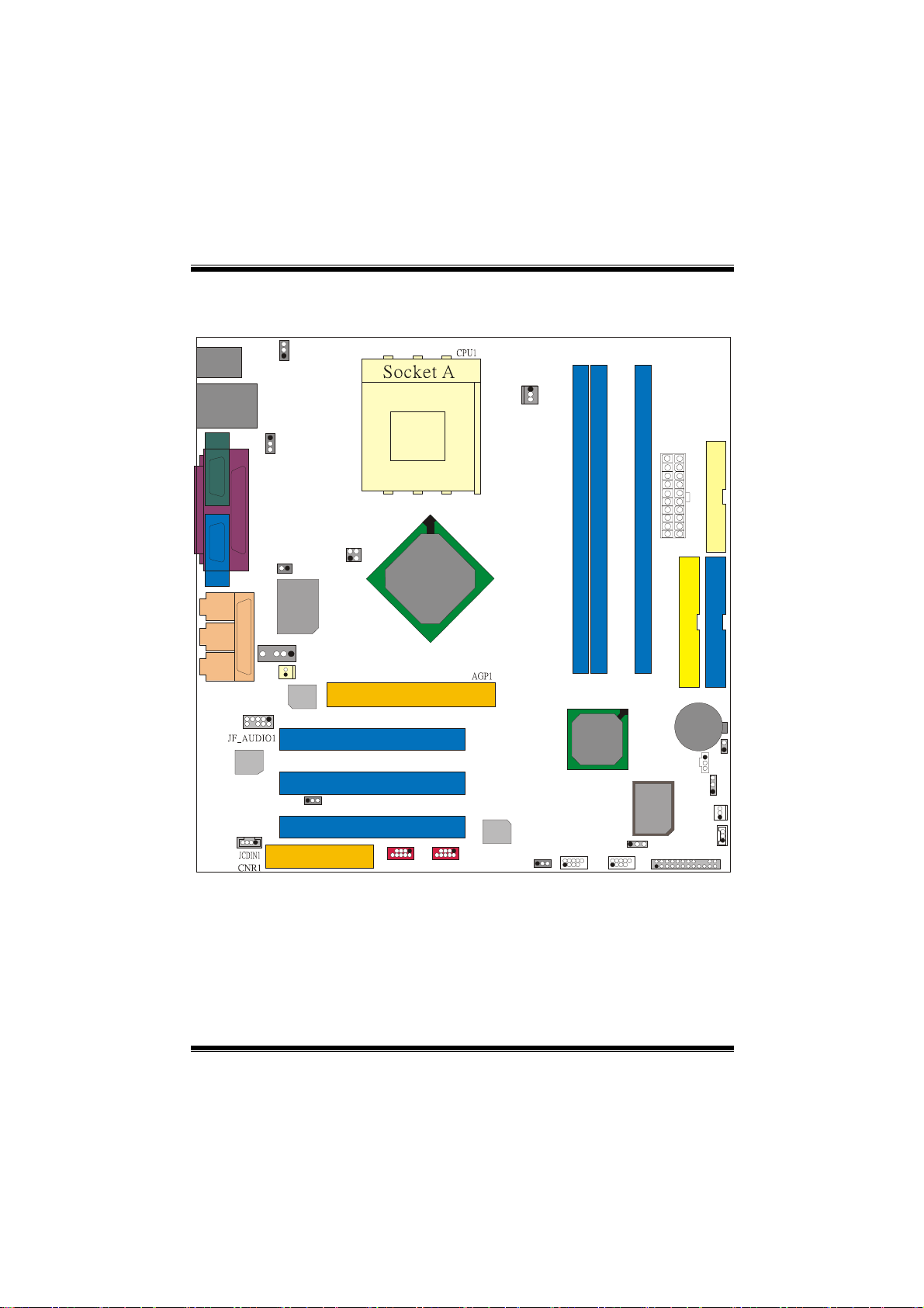
Layout of M7NCG 400
o
a
r
d
D
e
s
c
r
i
p
t
i
o
n
o
a
r
d
D
e
s
c
r
o
a
r
d
D
i
e
s
c
r
p
t
i
o
n
i
p
t
i
o
n
JKBMS1
JSPKR1
SP-OUT
JLIN1
LINE-IN
JMIC1
MIC-IN
JCOM1
JVGA1
GAME Port
JGAME1
9
10
Codec
Codec
CodecCodec
JUSBLAN1
1
JUSBV2
JPRNT1
Winbond
Winbond
WinbondWinbond
5
1
1
2
1
JKBV1
1
1
JCLK3
I/O
I/O
I/OI/O
1
Lan
LanLan
Chip
Chip
ChipChip
JDJ1
JNFAN1
Lan
1
JTV1
24
1
3
J_CODECSEL
9
10
J1394A
IGP
IGP
IGPIGP
1
9
10
2
PCI1
PCI2
PCI3
J1394B
1
JCFAN1
J_SPDIF1
JCMOS
JSFAN1
JPANEL1
SECONDARY IDE CONN.
BAT1
1
JWOL1
FDD1
IDE1IDE2
JC1
1
1
24
FLOPPY DISK CONN.
PRIMARY IDE CONN.
1
1
23
JATXPWER1
DIMMB1
MCP
MCP
MCPMCP
1394A
1394A
1394A1394A
Chip
Chip
ChipChip
(optional)
(optional)
tional)(optional
1
2
JUSBV1
1
JUSB1
2
1
10
DIMMB2
1
JUSB2
2
1
DIMMA1
BIOS
BIOS
BIOSBIOS
JUSBV4
10
1
2
3
Page 6
M
M
M
CPU Inst a l l ation
o
t
h
e
r
b
o
a
r
d
D
e
s
c
r
i
p
t
i
o
n
o
t
h
e
r
b
o
a
r
d
D
e
s
c
r
o
t
h
e
r
b
o
a
r
d
D
i
e
s
c
r
p
t
i
o
n
i
p
t
i
o
n
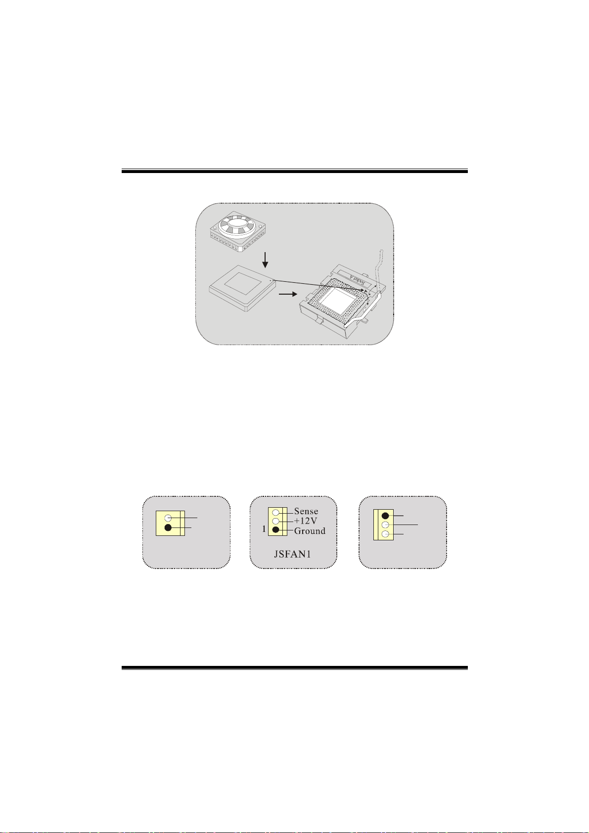
1. Pull the lever sideways away from the socket then raise the lever up to
90-degree angle.
2. Locate Pin A in the socket and lock for the white dot or cut edge in the CPU.
Match Pin A with the white dot/cut edge then insert the CPU.
3. Press the le ver do wn. The n Put the f an on the CPU and buc kle it and put the
fan’s power port into the JCFAN1, then to complete the installation.
C
P
U
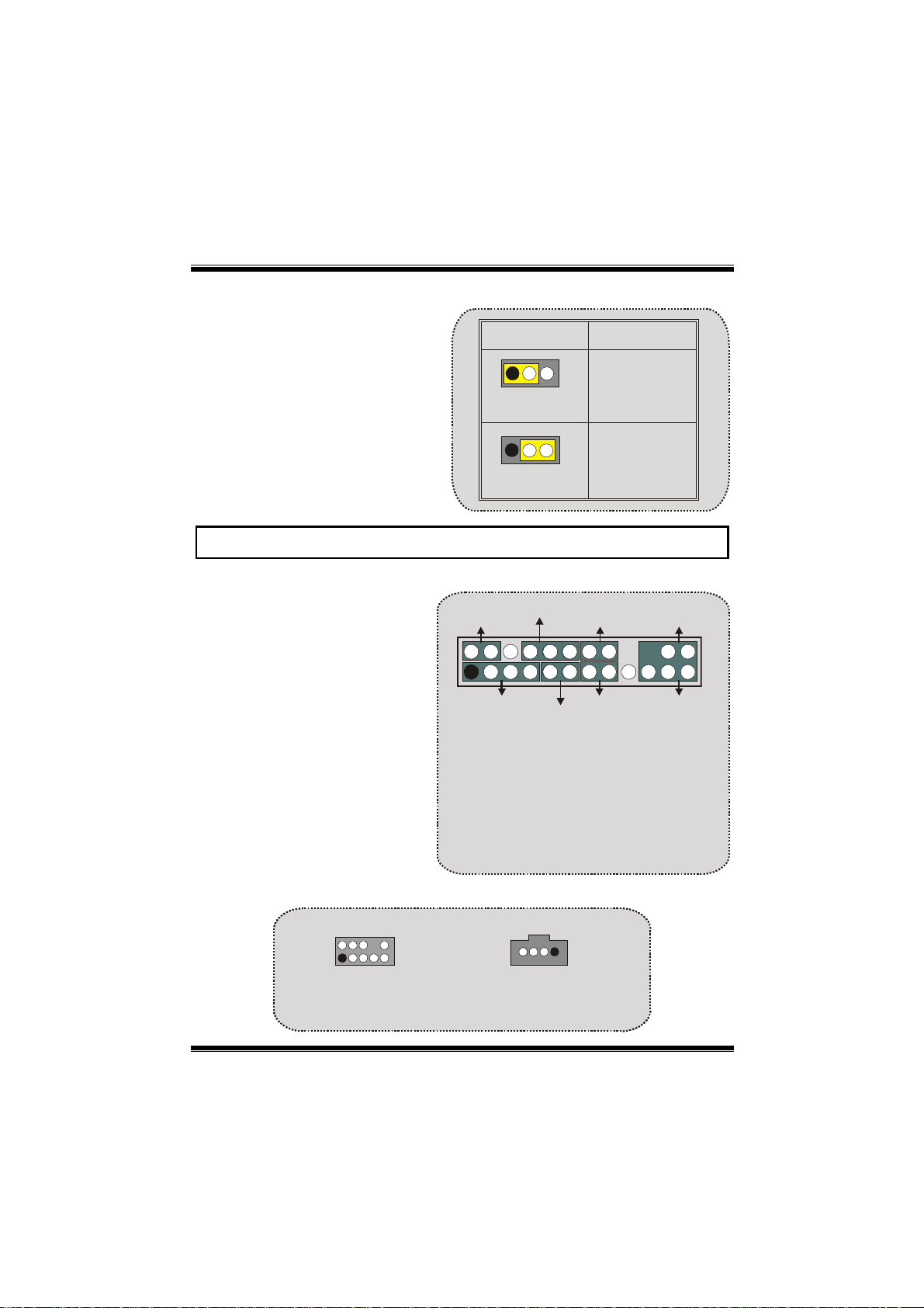
CPU/ System Fan Heade rs: JCFAN1/ JSFAN1/ JNFAN1
1
12V
Ground
JNFAN1
1
Ground
12V
Sense
JCFAN1
4
Page 7
M
o
t
h
e
r
b
o
a
r
d
D
e
s
c
r
i
p
t
i
o
n
M
M
o
t
h
e
r
b
o
a
r
d
D
e
s
c
r
o
t
h
e
r
b
o
a
r
d
D
i
e
s
c
r
p
t
i
o
n
i
p
t
i
o
n
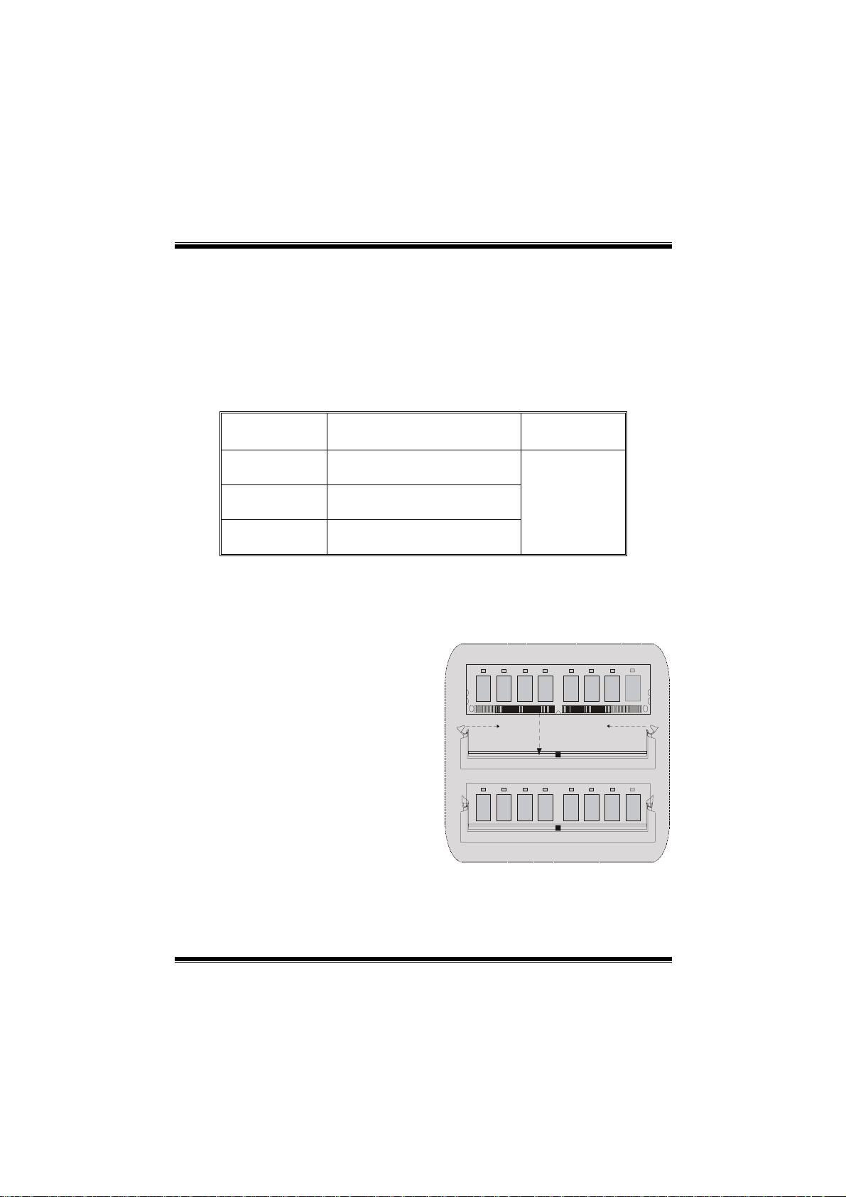
DDR DIMM Modules: DIMMB1/ DIM M B2 / DIMMA1
For Dual-channel DDR (128-bit) high performance, at least 2 or
more DIMM modules must be installed. (It has to be the
combination of DI MMA and DIMMB.) With onl y one DIMM installed,
the memory perform s onl y a t 64 - bit.
DRAM Access Time: 2.5V Unbuffered DDR 200/266/333 MHz Type required.
DRAM Type: 64MB/ 128MB/ 256MB/ 512MB/ 1GB DIMM Module (184 pin)
DIMM Socket
Location
DIMMB1 64MB/128MB/256MB/512MB/1GB
DIMMB2 64MB/128MB/256MB/512MB/1GB
DIMMA1 64MB/128MB/256MB/512MB/1GB
DDR Module Total Memory
Size (MB)
*1
Max is
*1
*1
~~~only for reference~~~
3GB
How to install a DIMM Module
1. The DIMM socket has a “ Plastic
Safety Tab”, and the DIMM memory
module has an “Asymmetrical notch”, so
the DIMM memory module can only fit
into the slot in one direct ion.
2. Push the tabs out. Insert the DIMM
memory modules into the socket at a
90-degree angle, then push down
vertically so that it will fit into the place.
3. The Mounting Holes and plastic tabs
should fit over the edge and hold the
DIMM memory modul es in place.
5
Page 8

M
o
t
h
e
r
b
o
a
r
d
D
e
s
c
r
i
p
t
i
o
n
M
M
o
t
h
e
r
b
o
a
r
d
D
e
s
c
r
o
t
h
e
r
b
o
a
r
d
D
i
e
s
c
r
p
t
i
o
n
i
p
t
i
o
n
Jumpers, Headers, Connectors & Slots
Hard Disk Connectors: IDE1/ IDE2
The motherboard has a 32-bit Enhanced PCI IDE Controller that provides PIO
Mode 0~4, Bus Master, and Ultra DMA / 33/ 66/ 100/ 133 functionality. It has two
HDD connectors IDE1 (primary) and IDE2 (secondary).
The IDE connectors can connect a master and a slave drive, so you can connect
up to four hard disk drives. The first hard drive should always be connected to
IDE1.
Floppy Disk Connector: FDD1
The motherboard provides a standard floppy disk connector that supports 360K,
720K, 1.2M, 1.44M and 2.88M floppy disk types. This connector supports the
provided floppy drive ribbon cables.
Communication Network Riser Slot: CNR1
The CNR specification is an open Industry Standard Architecture, and it defines a
hardware scalable riser card interface, which supports audio, network and modem
only.
Peripheral Component Interconnect Slots: PCI 1-3
This motherboard is equipped with 3 standard PCI slots. PCI stands for Peripheral
Component Interconnect, and it is a bus standard for expansion cards, which has,
supplanted the older ISA bus standard in most ports. This PCI slot is designated
as 32 bits.
AGP (Accelerated Graphics Port) Slot: AGP1
Your monitor will attach directly to that video card. This motherboard supports
video cards for PCI slots, but it is also equipped with an Accelerated Graphics Port
(AGP). An AGP card will take advantage of AGP technology for improved video
efficiency and performance, especially with 3D graphics.
Power Connectors: JATXPWER1
JATXPWR1
(ATX Main P ower Conn.)
JATXPWR1
(ATX Power Conn.)
6
Page 9
M
o
t
h
e
r
b
o
a
r
d
D
e
s
c
r
i
p
t
i
o
n
M
M
o
t
h
e
r
b
o
a
r
d
D
e
s
c
r
o
t
h
e
r
b
o
a
r
d
D
i
e
s
c
r
p
t
i
o
n
i
p
t
i
o
n
Wake On LAN Header:
JWOL1
1
Front USB Head e r: JUSB1/ JUSB2
2
1
JUSB 1/2
Pin As s ignment Pin Assignment
+5V +5V
12
Data (-)Data (-)
43
Data (+) Data (+)
56
Ground Ground
910
Key NA
87
5V/ 5V_SB Selection for Keyboard and Mouse: JKBV1
Note: 5V Standby only use for S3 Mode.
JKBV1
Pin 1-2 on
1
Pin 2-3 on
1
Assignment
5V
5V Standby
Wake up
Ground
5V_SB
JWOL1
Front 1394 Head e r: J1394A/ J1394B (optional)
J1394A/ B
Pin Assignment Pin Assignment
1
2
1
3
5
7
A+ AB+ B-
+12V +12V
9
7
2
4
6
8
10
GroundGround
GNDKEY
Page 10
M
o
t
h
e
r
b
o
a
r
d
D
e
s
c
r
i
p
t
i
o
M
M
o
t
h
e
r
b
o
a
r
d
D
e
s
o
t
h
e
r
b
o
a
r
d
c
D
e
s
c
n
r
i
p
t
i
o
n
r
i
p
t
i
o
n
5V/ 5V_SB Selection for USB: JUSBV 1/JU SBV2/
(JUSBV4=>optional)
Note: 5V Standby only use for S3 Mode.
JUSBV1/ 2/ 4
1
Pin 1-2 on
1
Pin 2-3 on
Front Pane l Connector:
JPANEL1
SLP
2
1
SPK ==> Speaker Conn.
HLED ==> Hard Driver LED
RST ==> Reset Button
IR ==> Infrared Conn.
SLP ==> Sleep Button
PWR_LED ==> Power LED
ON/ OFF ==> Power-on B utton
(+) (-)(+)
SPK
PWR_LED
(+) (-)
HLED
Audio Subsystem: JF_AUDIO1/ JCDIN1
2
2
1
1
JAUDIO1
JF_AUDIO1
(Front Audio He ade r )
(Front Audio He ade r )
JCDIN1
JCDIN1
(CD-ROM Audio-In Header)
(CD-ROM Audio-In Header)
Assignment
5V Standby
RST
1
1
5V
IRON/OFF
24
23
IR
8
Page 11

M
o
t
h
e
r
b
o
a
r
M
o
t
h
e
M
o
t
h
e
Pin
1
3
5
7
9
2
2
1
RT Line Out
LFT Line Out
Assignment
Mic In
Mic Power
Reserved
d
r
b
o
a
r
d
r
b
o
a
r
10
9
JF_AUDIO1 only support 2CH.
Front Panel Audio Connector/ Jumper Block
Jumper Setting Configurati on
12
4
3
5
7
9
12
3
5
7
9
Pin 5 and 6
6
Pin 9 and 10
10
4
6
No jumpers
installed
10
Audio line out signals are routed
to the back panel audio line out connector.
Audio line out and mic in signals are
available for front panel au dio connectors.
D
e
s
D
e
s
d
D
e
s
JF_AUDIO1
Pin
2
4
6
8
10
c
r
i
p
t
i
c
r
i
p
t
i
c
r
i
p
t
i
Assignment
Ground
Audio Power
RT Line Out
LFT Line Out
o
o
o
n
n
n
Key
Clear CMOS Jumper: JCMOS
JCMOS
Pin 1-2 on
1
Pin 2-3 on
1
Assignment
Normal
Operation
(default)
Clear CMOS
Data
9
Page 12

M
(
M
M
o
t
h
e
r
b
o
a
r
d
D
e
s
c
r
i
p
t
i
o
n
o
t
h
e
r
b
o
a
r
d
D
e
s
c
r
o
t
h
e
r
b
o
a
r
d
D
i
e
s
c
r
p
t
i
o
n
i
p
t
i
o
n
Remove AC
power line
AC power
on
JCMOS1
Pin2-3 close
Reset th e passwort as your will
or clear CMOS data
wait 15
seconds
JCMOS
Pin1-2 close
Frequency Se l e c t ion: JCLK3
Note: W hen overclock function failed and system is unable to boot-up, please
follow the instruction below:
1. Turn off the system.
2. Closed the JCLK3 jumper.
3. Turn on the system.
4. Enter CMOS setup menu and load defaults settings.
5. Turn off the system.
6. Open the JCLK3 jumper.
7. Turn on the system.
1
1
JCLK3
JCLK3
Open==> User mode
Open==> User mode (Default)
(Default)
Close==> Safe mode or
Close==> Safe mode (100MHz)
CPU Clock 100MHz
133/ 166/ 200 MHz)
Case Open Connector: JC1
1
Case Open
Signal
Ground
JC1
10
Page 13

M
o
t
h
e
r
b
o
a
r
d
D
e
s
c
r
i
p
t
i
o
n
M
M
o
t
h
e
r
b
o
a
r
d
D
e
s
c
r
o
t
h
e
r
b
o
a
r
d
D
i
e
s
c
r
p
t
i
o
n
i
p
t
i
o
n
CNR Codec Primary/Secondary Selection: J_CODECSEL
J_CODECSEL
Pin 1-2 On-board Primary
Codec.
1
Pin 2-3 CNR Primary Codec.
1
Assignment
Digital Audio Connector: J_SPDIF1
SPDIF_OUT
GNDVCC5
1
J_SPDIF1
Audio DJ Header: JDJ1 (optional)
JDJ1
Pin1 ==> SMBDT
1
Pin2 ==> SMBCK
Pin3 ==> -INTR_B
Pin4 ==> Key
5
Pin5 ==> PWRGD
TV Out Header: JTV1 (optional)
24
1
JTV1
Pin1 ==> TV_Y
Pin2 ==> Ground
3
Pin3 ==> Ground
Pin4 ==> TV_C
11
Page 14
M
o
t
h
e
M
o
t
h
e
M
o
t
h
e
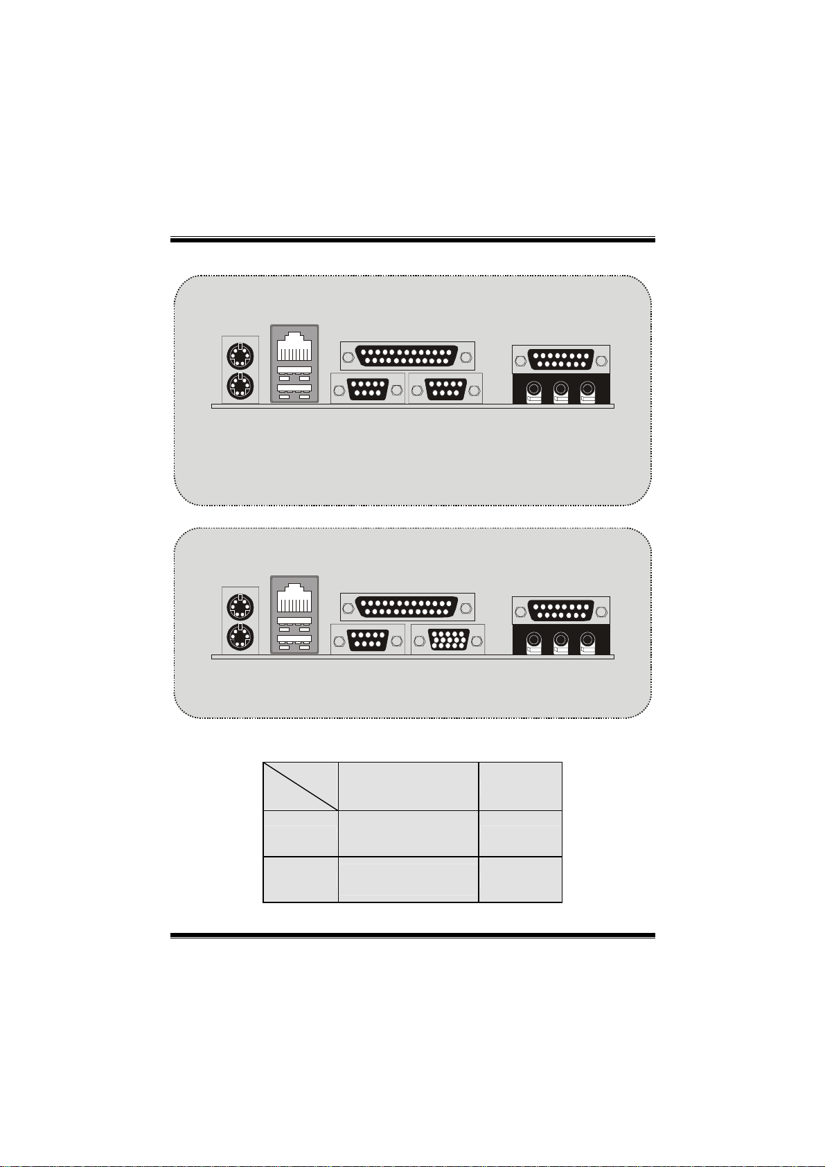
Back Panel Connectors
r
b
o
a
r
d
D
e
s
c
r
i
p
t
i
o
n
r
b
o
a
r
d
D
e
s
c
r
r
b
o
a
r
d
D
i
e
s
c
r
p
t
i
o
n
i
p
t
i
o
n
JKBMS1
PS/2
Mouse
PS/2
Keyboard
JKBMS1
PS/2
Mouse
PS/2
Keyboard
JUSBLAN1
LAN(Optional)
USB
JUSBLAN1
LAN(Optional)
USB
COM1
JCOM1
COM1
JCOM1
JPRNT1 JGAME1
Parallel
COM2
(optional)
JCOM2
(optional)
JPRNT1 JGAME1
Parallel
VGA1
JVGA1
Speaker
Speaker
Out
Out
Game Port
Line In
Game Port
Line In
Mic
In
Mic
In
The LED indicator for La n port status:
Status
Speed
10Mbps
100Mbps
Normal Download
Right light: green
Left light: no
Right light: green
Left light: orange
12
Light: blink
Light: blink
Page 15

M
o
t
h
e
r
b
o
a
r
d
D
e
M
M
o
t
h
e
r
b
o
o
t
h
a
e
r
b
o
a
s
r
d
D
e
s
r
d
D
e
s
Español
Características del M7NCG 400
c
r
i
p
t
i
o
n
c
r
i
c
r
p
t
i
o
n
i
p
t
i
o
n
CPU
- Soporta procesador AMD
- Corriendo a 200/266/333/400MHz FSB.
Chipset
- North Bridge: nFORCE2 Crush18G IGP Chipset.
- South Bridge: MCP Chipset.
High Speed 800Mb/s Hyper-Transport interface para el
MCP.
Memoria Principal
- Soporta hasta 3 dispositivos DDR.
- Soporto 200/266/333MHz (sin ECC) dispositivos DDR.
- High performance 128-bit DDR333 Twin Bank Memory Architecture.
- Capacidad máxima de memoria es 3GB.
Ranuras
- Tres ranuras de 32-bit PCI bus master.
- Una ranura CNR.
- Una ranura AGP: AGP3.0 8X interface a 533Mb/s.
Soporta AGP 4X, 8X.
On Board IDE
- Soporta cuatro discos IDE.
- Soporta Modo 4 PIO, Modo Master y Ultra DMA 33/66/100/133 Bus Modo
Master.
On Board VGA
- GeForce 4MX Series Unidad Gráficos de Proceso (GPU).
Chip 1394 (opcional)
- Realtek 8801BL.
- Soporta 2 puertos con transferencia de hasta 400Mbps.
Audio
- Interface AC97 2.2.
- PC99 complaint.
- Soports 6 canales.
- S/PDIF Out.
TV Out (opcional)
- Soporta modo s-video output.
®
Zócalo 462 de hasta XP 3200+.
13
Page 16

M
o
t
h
e
r
b
o
a
r
d
D
e
s
c
r
i
p
t
i
o
n
M
o
t
h
e
r
b
o
a
r
d
D
e
s
c
r
M
o
t
h
e
r
b
o
a
r
d
D
- Resolución de pantalla de hasta 1024 x 768 (incluyendo todos los modos
DOS)
- Soporta formatos de TV: NTSC-M (América del Norte y Taiwan)
NTSC-J (Japón)
PAL (Europa y Asia)
Periféricos On Board
- Soporta 360K, 720K, 1.2MB, 1.44MB y 2.88MB unidad de disquete
- Soporta 2 puertos serie.
- Soporta 1 multi-modo del puerto paralelo (modos SPP/EPP/ECP)
- Soporta ratón PS/2 y teclado PS/2.
- Soporta 2 puertos USB2.0 traseros y 4 puertos USB2.0 delanteros.
- Soporta conector S/PDIF Out.
BIOS
- AWARD legal Bios.
- Soporta APM1.2.
- Soporta ACPI.
- Soporta función USB.
Sistemas Operativos
- Ofrece alto rendimiento en MS-DOS, Windows 2000, Windows Me,
Windows XP, SCO UNIX etc.
Dimensión
- Factor de Forma Micro ATX: 24.4cm X 24.4cm (W X L)
i
e
s
c
r
p
t
i
o
n
i
p
t
i
o
n
Contenido del Paquete
- Cable HDD X 1
- Cable FDD X 1
- Configuración Completa del Driver CD X 1
- Manual del Usuario X 1
- Cable USB X 2 (opcional)
- Cable SPDIF OUT X1 (opcional)
- Cable IEEE 1394 X1 (opcional)
14
Page 17

M
9
9
(op
)
o
t
h
e
r
b
o
a
r
d
M
M
o
t
h
e
r
b
o
t
h
e
r
b
D
o
a
r
d
D
o
a
r
d
D
Disposición del M7NCG 400
JKBMS1
JKBV1
1
e
s
c
r
i
p
t
i
o
n
e
s
c
r
i
e
s
c
r
p
t
i
o
n
i
p
t
i
o
n
JSPKR1
SP-OUT
JLIN1
LINE-IN
JMIC1
MIC-IN
JCOM1
JVGA1
GAME Port
JGAME1
9
10
Codec
Codec
CodecCodec
JUSBLAN1
1
JUSBV2
JPRNT1
Winbond
Winbond
WinbondWinbond
5
1
1
2
1
1
JCLK3
I/O
I/O
I/OI/O
1
JDJ1
JNFAN1
Lan
Lan
LanLan
Chip
Chip
ChipChip
1
JTV1
24
1
3
J_CODECSEL
9
10
J1394A
IGP
IGP
IGPIGP
1
9
10
2
PCI1
PCI2
PCI3
J1394B
1
JCFAN1
J_SPDIF1
JCMOS
JSFAN1
JPANEL1
SECONDARY IDE CONN.
BAT1
1
JWOL1
FDD1
IDE1IDE2
JC1
1
1
24
FLOPPY DISK CONN.
PRIMARY IDE CONN.
1
1
23
JATXPWER1
DIMMB1
MCP
MCP
MCPMCP
1394A
1394A
1394A1394A
Chip
Chip
ChipChip
(optional)
(optional)
tional)(optional
1
2
JUSBV1
1
JUSB1
2
1
10
DIMMB2
1
JUSB2
2
1
DIMMA1
BIOS
BIOS
BIOSBIOS
JUSBV4
10
1
2
15
Page 18

M
o
t
h
e
M
M
r
o
t
h
e
r
o
t
h
e
r
Instalación de la CPU
b
o
a
r
d
D
e
s
c
r
i
p
t
i
o
n
b
o
a
r
d
D
e
s
c
r
b
o
a
r
d
D
i
e
s
c
r
p
t
i
o
n
i
p
t
i
o
n
1. Tire de la palanca del lado del zócalo, luego levante la palanca hasta un
ángulo de 90 grados.
2. Sitúe el contacto A del zócalo y busque el punto blanco o corte el borde en la
CPU. Empareje el contacto A con el punto blanco/ corte del borde, luego
inserte la CPU.
3. Presione la palanca para abajo. Ponga el ventilador en la CPU y abróchelo.
Luego ponga el puerto de corriente del ventilador en el JCFAN1. Y ya habrá
completado su instalación.
C
P
U
CPU/ Cabezal del Sistema de Ventilación: JCFAN1/ JSFAN1/
JNFAN1
12V
1
Tier r a
1
Tier r a
12V
Sense
JNFAN1
16
JCFAN1
Page 19

M
o
t
h
e
r
b
o
a
r
d
D
e
s
c
r
i
p
t
i
o
n
M
M
o
t
h
e
r
b
o
a
r
d
D
e
s
c
r
o
t
h
e
r
b
o
a
r
d
D
i
e
s
c
r
p
t
i
o
n
i
p
t
i
o
n
Módulos DDR DIMM: DIMMB1/DIMMB2/
DIMMA1
Para un al to fun cionam iento, Dual -chann el DD R (128 -bit) , po r
lo menos 2 o más módulos DIMM debe ser instalado. (Tiene
que ser l a co mbin ació n d el D I MMA y DI MMB.) Con so lam ent e
un DIMM instalado, la memoria funciona solamente a 64-bit.
DRAM Tiempo de Acceso: 2.5V Unbuffered DDR 200/266/333 MHz Tipo
requerido.
DRAM Tipo: 64MB/ 128MB/ 256MB/ 512MB/ 1GB Módulos DIMM (184 contactos)
Localización
del Zócalo
DIMM
DIMMB1 64MB/128MB/256MB/512MB/1GB
DIMMB2 64MB/128MB/256MB/512MB/1GB
Módulo DDR Total del
Memoria (MB)
*1
*1
~~~solamente para referencia~~~
Tamaño de
Máximo 3GB
Cómo instalar un módulo DIMM
1. El zócalo DIMM tiene una lengüeta
plástica de seguridad y el módulo de
memoria DIMM tiene una muesca
asimétrica, así el módulo de memoria
DIMM puede caber solamente en la
ranura de una sóla dirección.
2. Tire la lengüeta hacia afuera. Inserte
los módulos de memoria DIMM en el
zócalo a los 90 grados, luego empuje
hacia abajo verticalmente de modo que
encaje en el lugar.
3. Los agujeros de montaje y las
lengüetas plásticas deben caber por
sobre el borde y sostenga los módulos
de memoria DIMM en el lugar.
17
Page 20

M
o
t
h
e
r
b
o
a
r
d
D
e
s
c
r
i
p
t
i
o
n
M
M
o
t
h
e
r
b
o
a
r
d
D
e
s
c
r
o
t
h
e
r
b
o
a
r
d
D
i
e
s
c
r
p
t
i
o
n
i
p
t
i
o
n
Conectores, Cabezales, Puentes y Ranuras
Conectores del Disco Duro: IDE1/ IDE2
La placa madre tiene un controlador de 32-bit PCI IDE que proporciona Modo PIO
0~4, Bus Master, y funcionalida Ultra DMA / 33/ 66/ 100. Tiene dos conectores
HDD IDE1 (primario) y IDE2 (secundario).
El conector IDE puede conectar a un master y un drive esclavo, así puede
conectar hasta cuatro discos rígidos. El primer disco duro debe estar siempre
conectado al IDE1.
Conector para el Disquete: FDD1
La placa madre proporciona un conector estándar del disquete (FDC) que soporta
360K, 720K, 1.2M, 1.44M y 2.88M tipos de disquete. Éste conector utiliza los
cables de cinta proporcionados por el disquete.
Ranura de Banda de Suspensión de Comunicación y Red: CNR1
La especificación CNR es una abierta Industria Estándar de Arquitectura, y define
una tarjeta hardware escalable de interface en el que soporta audio, red y
módem.
Ranura de Interconexión del Componente Periférico: PCI 1-3
Ésta placa madre está equipado con 3 ranuras PCI. PCI es la sigla para
Interconexión del Componente Periférico, y es un estándar bus para la tarjeta de
expansión en el que reemplaza, en su mayoría de las partes, al antiguo estándar
ISA bus. Las ranuras de PCI están desiñados con 32 bits.
Ranura del Puerto Acelerado para Gráficos: AGP1
Su monitor se fijará directamente a la tarjeta de video. Ésta placa madre soporta
tarjetas de video para ranuras PCI, y también está equipado con un Puerto
Acelerado para Gráficos (AGP/ solamente soporta 1.5V y 4X tarjeta AGP). Ésta
tarjeta AGP tomará ventaja de la tecnología del AGP para el mejoramiento de la
eficiencia y funcionamiento del video, especialmente con gráficos 3D.
Conector de Corriente: JATXPWER1
JATXPW R1
(Conector de
Corriente ATX)
18
Page 21

M
o
t
h
e
r
b
o
a
r
d
D
e
s
c
r
i
p
t
i
o
n
M
M
o
t
h
e
r
b
o
a
r
d
D
e
s
c
r
o
t
h
e
r
b
o
a
r
d
D
i
e
s
c
r
p
t
i
o
n
i
p
t
i
o
n
Cabezal Wake On LAN:
JWOL1
Cabezal Frontal USB: JUSB1/ JUSB2
Contactos Asignacion Contactos Asignacion
2
1
12
56
910
+5V +5V
Data (+) Data (+)
Tierra Tierra
JUSB1/2
43
87
Key NA
Data (-)Data (-)
5V/ 5V_SB Selección para Teclado y Ratón: JKBV1
Nota: 5V Standby solamente para el modo S3.
JKBV1
Contactos
1-2 on
1
Contactos
2-3 on
1
Asignacion
5V
5V Standby
1
Wake up
5V_SB
JWOL1
Tierra
Cabezal Frontal 139 4: J1394A/ J1394B (opcional)
J1394A/ B
ContactosAsignacion Contacto s Asignacion
1
1
3
2
5
7
A+ AB+ B-
+12V +12V
9
19
2
4
6
8
10
TierraTierra
GNDKEY
Page 22

M
o
t
h
e
r
b
o
a
r
d
D
e
s
c
r
i
p
t
i
o
n
M
M
o
t
h
e
r
b
o
a
r
d
D
e
s
c
r
o
t
h
e
r
b
o
a
r
d
D
i
e
s
c
r
p
t
i
o
n
i
p
t
i
o
n
5V/ 5V_SB Selección para USB: JUSBV 1/J USBV2/
(JUSBV4=>opcional)
Nota: 5V Standby solamente para el modo S3.
JUSBV1/ 2/ 4
1
Contactos
1-2 on
1
Contactos
2-3 on
Conector del Panel Frontal: JPANEL1
2
1
SPK ==> Conector de Altavoz
HLED ==> LED del Disco Duro
RST ==> Boton de Reinicio
IR ==> Conector Infrarojo
SLP ==> Boton de Suspension
PWR_LED ==> Corriente LED
ON/ OFF ==> Boton de Encendido
SLP
SPK
PWR_LED
(+) (-)(+)
(+) (-)
HLED
RST
IRON/OFF
24
23
IR
Subsistema de Audio: JF_AUDIO1/ JCDIN1
(Cabezal de Audio Frontal)
2
1
JF_AUDIO1
JCDIN1
(Cabe z al de Entrad a de
Audio CD-ROM)
Asignacion
5V
5V Standby
1
20
Page 23

M
o
t
h
e
r
b
o
a
r
d
D
e
s
c
r
i
p
t
i
o
n
M
o
t
h
e
r
b
o
a
r
d
D
e
s
c
r
M
o
t
h
e
r
b
o
a
r
d
D
i
e
s
c
r
p
t
i
o
n
i
p
t
i
o
n
10
9
JF_AUDIO1
Contactos
2
4
6
8
10
Contactos
2
2
1
Asignacion
1
3
5
7
9
Entrada de l MIC
Corriente del MIC
RT Salida de Line a
Reservado
LFT Salida de Linea
JF_AUDIO1 only support 2CH.
Conector del Panel Frontal de Audio/ Jumper Block
Jumper Setting Configur acion
~
12
4
3
6
5
7
10
9
12
4
3
6
5
7
10
9
Contacto 5 & 6
Contacto 9 & 10
No jumpers
installed
La senal de salida de linea del Audio
encamina al conector de la salida de linea
del Audio ubicado en el panel trasero.
~
La senal de salida de linea del Audio y la
~
senal del entr ada del mic estan disponibles
desde el conector de Audio del
panel frontal.
Asignacion
Tierra
Corriente de Audio
R T Salida de Linea
Key
LFT Salida de Linea
Clear CMOS Jumper: JCMOS
JCMOS
Contacto
1-2 on
1
Contacto
2-3 on
1
Asignacion
Operacion
Normal
(default)
Borrar Datos
CMOS
21
Page 24

M
)
M
M
o
t
h
e
r
b
o
a
r
d
D
e
s
c
r
i
p
t
i
o
n
o
t
h
e
r
b
o
a
r
d
D
e
s
c
r
o
t
h
e
r
b
o
a
r
d
D
i
e
s
c
r
p
t
i
o
n
i
p
t
i
o
n
Quite el cable
de corriente
del AC
Encienda
AC
JCMOS1
Contactos
2-3 cerrado
Reconfigure la contrasena
deseada o borre datos CMOS
Espere 15
segundos
JCMOS
Contacto s
1-2 ce rrad o
~
Selección de Frecuencia: JCLK3
Nota: Cuando la func ión del over clock falla y el sistem a no pueda encende rse,
por favor siga las sigientes instrucciones:
1. Apague el sistema.
2. Inserte el puente JCLK3 en cerrado.
3. Prenda el sistema.
4. Entre al menu de la configuración del CMOS y cargue las conf iguraciones
5. Apague el sistema.
6. Inserte el puente JCLK3 en abierto.
7. Prenda el sistema.
1
1
JCLK3
JCLK3
defaults.
Open==> User mode
Open==> Modo para el Usuario (Default
(Default)
(133/ 166/ 200 MHz)
Close==> Safe mode or
Close==> Modo Safe (100MHz)
CPU Clock 100MHz
Conector de la Carcasa Abierta: JC1
1
~
Senal del
Case Open
Tierra
JC1
22
Page 25

M
o
t
h
e
r
b
o
a
r
d
D
e
s
c
r
i
p
t
i
o
n
M
M
o
t
h
e
r
b
o
a
r
d
D
e
s
c
r
o
t
h
e
r
b
o
a
r
d
D
i
e
s
c
r
p
t
i
o
n
i
p
t
i
o
n
Selección CNR Codec Primario/ Secundario: J_CODECSEL
J_CODECSEL
Contacto
1
1
1-2
Contacto
2-3
Asignacion
Codec P rimar io
integrado en la placa madre.
CNR Codec Primario.
Conector Digital de Audio: J_SPDIF1
SPDIF_OUT
GNDVCC5
1
J_SPDIF1
Cabezal de Audio DJ: JDJ1 (opcional)
JDJ1
Contacto1 ==> SMBDT
1
Contacto2 ==> SMBCK
Contacto3 ==> -INTR_B
Contacto4 ==> NC
5
Contacto5 ==> PWRGD
Cabezal TV Out: JTV1 (opcional)
24
1
JTV1
Contacto1 ==> TV_Y
Contacto2 ==> Tierra
3
Contacto3 ==> Tierra
Contacto4 ==> TV_C
23
Page 26

M
o
t
h
e
r
b
o
a
M
M
o
t
h
e
o
t
h
e
r
r
b
o
a
r
r
b
o
a
r
Conectores del Panel Trasero
d
D
e
s
c
r
i
p
t
i
o
n
d
D
e
s
c
r
d
D
i
e
s
c
r
p
t
i
o
n
i
p
t
i
o
n
JKBMS1
Raton
PS/2
Teclado
PS/2
JKBMS1
Raton
PS/2
Teclado
PS/2
JUSBLAN1
LAN
(Opcional)
USB
JUSBLAN1
LAN(Opcional)
USB
JPRNT1 JAUD_GAME
Puerto Paralelo Puerto d e J uego
COM1
JCOM1
VGA1
JVGA1
Salida del
Altavoz
JPRNT1 JGAME1
Puerto de Juego
Salida del
Altavoz
COM1
JCOM1
Paralelo
COM2
(opcional)
JCOM2
(opcional)
Entrada
de Linea
Entrada
de Linea
Entrada de
Mic
Entrada de
Mic
Estado del Indicador LED del LAN:
Estado
Velocidad
10Mbps
100Mbps
Indicador Derecho: Verde
Indicador Izqui e rdo: Nada
Indicador Derecho: Verde
Indicador Izquierdo: Naranja
Normal Bajando Datos
Luz: Parpadeando
Luz: Parpadeando
24
Page 27

M
o
t
h
e
r
b
o
a
r
d
D
e
s
c
r
i
p
t
i
o
n
M
M
o
t
h
e
r
b
o
a
r
d
D
e
s
c
r
o
t
h
e
r
b
o
a
r
d
D
i
e
s
c
r
p
t
i
o
n
i
p
t
i
o
n
Deutsch
M7NCG 400 Features
CPU
- Unterstützung für AMD Prozessor(Sockel462 ) bis zu XP 3200+.
- FSB mit 200/266/333/400MHz..
Chipsatz
- Northbridge: nFORCE2 Crush 18G IGP Chipsatz.
- Southbridge: MCP.
Hauptspeicher
- Unterstützung für 3 DDR Geräte.
- Unterstützung für 200/266/333MHz (ohn e EC C) DDR Geräte.
- 128-bit High-Performance DDR333 mit der Tw in- Bank Architektur.
- Die maximale Speichergröße ist 3GB.
Slots
- Drei 32-Bit PCI -Bus-Slots.
- Ein CNR-Slot.
- Ein AGP-Slot: AGP3.0 8X Interface mi t 533Mb/s.
Unterstützung für AGP 4X, 8X.
On Board IDE
- Unterstützung für vier IDE Diskettenlaufwerke.
- Unterstützung für PIO Modus 4, Master Modus und Ultra DMA
33/66/100/133 Bus Master Modus.
On Board VGA
- GeForce 4MX Series graphics processing unit(GPU).
1394 Chip (optional)
- Realtek 8801Bl mit drei 1394 Anschlüssen unterstützt bis zu 400Mbit/s
Transferrate.
Audio
- AC97-2.2-Interface.
- PC99 kompatibel.
- Unterstützung für 6-Kanal.
- S/PDIF Ausgabe.
TV-Ausgabe (optional)
- Unterstützung für S-Video Ausgabe Modus.
800Mb/s Hohe Geschwindigkeit : Hyper-Transport
-Interface zu den MCP Chipsatz.
25
Page 28

M
o
t
h
e
r
b
o
a
r
d
D
e
s
c
r
i
p
t
i
o
n
M
o
t
h
e
r
b
o
a
r
d
D
e
s
c
r
M
o
t
h
e
r
b
o
a
r
d
D
- Anzeige Auflösung bis zu 1024 x 768 (enthält alle D OS -Modi)
- Unterstützung für die TV Formate: NTSC-M (Norden Amerika und Tai wan)
NTSL-J (Japan)
PAL (Europa und Asien)
On Board Peripherals
- 1 Floppy-Port mit Unterstützung für 2 Diskettenlaufwerke.(360KB, 720KB,
1.2MB, 1.44MB und 2.88MB)
- 2 serielle Schnittstellen.
- 1 parallele Schnittstelle mit Unters tützung für SPP/EPP/ECP-Modus.
- Unterstützung für PS/2-Maus und PS/2 -Tastatur.
- Unterstützung für sechs USB2.0-Ports. (hintenX 4, vornX2)
- Unterstützung für S/PDIF Ausgabe Anschluss.
BIOS
- Unterstützung für AWARD legal Bios.
- Unterstützung für APM1.2.
- Unterstützung für ACPI.
- Unterstützung für USB Function.
Operating System
- Unterstützung für die am meisten verbreiteten Betriebsysteme wie Windows
2000, Windows ME, Windows XP, LINUX and SCO UNIX.
Dimensions
- Micro ATX Form-Factor: 24.4cm X 24.4cm (W X L)
i
e
s
c
r
p
t
i
o
n
i
p
t
i
o
n
Verpackungsinhalt
- HDD Kable X 1
- FDD Kable X 1
- Treiber CD für Install ationX 1
- Benutzer Handbuch X 1
- USB Kable X 2 (optional)
- I/O-Rückwand für ATX Gehäuse X 1 (optional)
- SPDIF-Ausgang-Kabl e X1 (optional)
- IEEE 1394 Kable X1 (opt ional)
26
Page 29

M
9
9
(op
)
o
t
h
e
r
b
o
a
r
d
M
M
o
t
h
e
r
b
o
t
h
e
r
b
D
o
a
r
d
D
o
a
r
d
D
Layout des M7NCG 400
e
s
c
r
i
p
t
i
o
n
e
s
c
r
i
e
s
c
r
p
t
i
o
n
i
p
t
i
o
n
JKBMS1
JSPKR1
SP-OUT
JLIN1
LINE-IN
JMIC1
MIC-IN
JCOM1
JVGA1
GAME Port
JGAME1
9
10
Codec
Codec
CodecCodec
JUSBLAN1
1
JUSBV2
JPRNT1
Winbond
Winbond
WinbondWinbond
5
1
1
2
1
JKBV1
1
1
JCLK3
I/O
I/O
I/OI/O
1
Lan
LanLan
Chip
Chip
ChipChip
JDJ1
JNFAN1
Lan
1
JTV1
24
1
3
J_CODECSEL
9
10
J1394A
IGP
IGP
IGPIGP
1
9
10
2
PCI1
PCI2
PCI3
J1394B
1
JCFAN1
J_SPDIF1
JCMOS
JSFAN1
JPANEL1
SECONDARY IDE CONN.
BAT1
1
JWOL1
FDD1
IDE1IDE2
JC1
1
1
24
FLOPPY DISK CONN.
PRIMARY IDE CONN.
1
1
23
JATXPWER1
DIMMB1
MCP
MCP
MCPMCP
1394A
1394A
1394A1394A
Chip
Chip
ChipChip
(optional)
(optional)
tional)(optional
1
2
JUSBV1
1
JUSB1
2
1
10
DIMMB2
1
JUSB2
2
1
DIMMA1
BIOS
BIOS
BIOSBIOS
JUSBV4
10
1
2
27
Page 30

M
o
t
h
e
r
M
M
b
o
t
h
e
r
b
o
t
h
e
r
b
Installation der CPU
o
a
r
d
D
e
s
c
r
i
p
t
i
o
n
o
a
r
d
D
e
s
c
r
o
a
r
d
D
i
e
s
c
r
p
t
i
o
n
i
p
t
i
o
n
1. Ziehen Sie den Hebel seitwärts von der Sockel und neigen Sie ihn um
90-Grad nach oben.
2. Suchen Sie Pin A im Sockel und den weißen Punkt oder die Abschnittkante in
der CPU. Passen Sie Pin A mit dem weißen Punkt/der Abschnittkante
zusammen und legen Sie danach die CPU ein.
3. Drücken Sie den Hebel nach unten. Befestigen Sie danach den Lüfter auf die
CPU und schließen Sie die Stromschnittstelle des Lüfters an JCFAN1 an und
beenden Sie die Installation.
C
P
U
CPU/ System Fan Headers: JCFAN1/ JSFAN1/ JNFAN1
12V
1
GND
1
GND
12V
Sensor
JNFAN1
28
JCFAN1
Page 31

M
o
t
h
e
r
b
o
a
r
d
D
e
s
c
r
i
p
t
i
o
n
M
M
o
t
h
e
r
b
o
a
r
d
D
e
s
c
r
o
t
h
e
r
b
o
a
r
d
D
i
e
s
c
r
p
t
i
o
n
i
p
t
i
o
n
DDR-DIMM-Modules: DIMMB1/DIMMB2/
DIMMA1
Für Dual-Kanal DDR(128bit) High-Performance mußt man
mindenstens zwei oder mehr DIMM-Modules installieren. (Der
Speicher mußt in der Kombination von DIMMA und DIMMB
installier t werd en.)
DRAM Zugriffszeit : 2.5V unbuffered DDR 200/266/333 MHz Typen erfordert.
DRAM Typen: 64MB/ 128MB/ 256MB/ 512MB/ 1GB DIMM-Module (184 pin)
DIMM-Sockel
Standort
DIMMB1 64MB/128MB/256MB/512MB/1GB
DIMMB2 64MB/128MB/256MB/512MB/1GB
DIMMA1 64MB/128MB/256MB/512MB/1GB
~~~DRAM-Konfiguration wird als Referenz~~~
DDR-Module Speichergröße
(MB)
*1
maximal
*1
*1
3GB
Installation von DIMM-Modulen
1. DDR DIMM hat nur eine Passkerbe in
der Mitte des Moduls. Das Modul passt
nur in einer Richtung.
2. Ziehen Sie die Plastikklammer an
beiden Enden der DIMM-Steckplätze
aus, dann setzen Sie das DIMM-Modual
im 90-Grad-Winkel in den
DIMM-Steckplatz und drücken es nach
unten.
3. Schließen Sie die Plastikklammer, um
das DiMM-Modul zu verriegeln.
29
Page 32

M
o
t
h
e
r
b
o
a
r
d
D
e
s
c
r
i
p
t
i
o
n
M
M
o
t
h
e
r
b
o
a
r
d
D
e
s
c
r
o
t
h
e
r
b
o
a
r
d
D
i
e
s
c
r
p
t
i
o
n
i
p
t
i
o
n
Jumper, Header, Anschlüsse & Slots
Festplattenanschlüsse: IDE1 und IDE2
Das Mainboard hat einen 32-Bit Enhanced PCI IDE-Controller, der die Modi
PIO0~4, Bus M aster sowie die Ultra DMA/33/66/100/133- Funktion zur Verfügung
stellt. Dieser ist mit zweii HDD-Anschlüssen versehen IDE1 (primär) und IDE2
(sekundär).
Die IDE-Anschlüsse können eine Master- und eine Slave-Festplatte verbinden, so
dass bis zu 4 Festplatten angeschlossen werden können. Die erste Festplatte
sollte immer an IDE1 angeschlossen werden.
Diskettenanschluss: FDD1
Das Motherboard enthält einen standardmäßigen Diskettenanschluss, der 360K-,
720K-, 1.2M-, 1.44M- und 2.88M-Disketten unterstützt. Dieser Anschluss
unterstützt die mitgelieferte Bandkabel des Diskettenlaufwerks.
Communication Network Riser Slot: CNR1
Die CNR-Angaben entsprechen einer offenen Industry Standar d Archite cture, und
sie definieren eine Hardware-skalierbare Riser-Card-Schnittstelle, welche nur
Audio, Netzwerk und Modem unterst ützt.
Peripheral Component Interconnect Slots: PCI 1-3
Dieses Motherboard ist mit 3 standardmäßigen PCI-Slots ausgestattet. PCI steht
für Peripheral Component Interconnect und bezieht sich auf einem Busstandard
für Erweiterungskarten, der den älteren ISA-Busstandard in den meisten
Schnittstell en ersetzt hat. Dieser PCI-Slot ist für 32 bits vorgesehen.
Accelerated Graphics Port Slot: AGP1
Ihr Monitor wird direkt an die Grafikkarte angeschlossen. Dieses Motherboard
unterstützt Grafikkarten für PCI-Slots, aber es ist auch mit einem Accelerated
Graphics Port ausgestattet. AGP-Karten verwenden die AGP-Technologie, um die
Wirksamkeit und Leistung von Videosignalen zu verbessern, besonders wenn es
sich um 3D-Grafiken handelt.
Stromversorgungsanschluss: JATXPWR1
JATXPWR1
(ATX Stromversorgungs-
anschluss)
30
Page 33

M
N
o
t
h
e
r
b
o
a
r
d
D
e
s
c
r
i
p
t
i
M
M
o
t
h
e
r
b
o
a
r
d
D
e
o
t
h
e
r
b
o
a
s
r
d
D
e
s
o
c
r
i
p
t
i
o
c
r
i
p
t
i
o
Wake On LAN Header:
JWOL1
Front USB Head e r: JUSB1/ JUSB2
2
1
JUSB 1/2
Pin Beschreibung Pin
12
+5V
43
56
Data (+) Data (+ )
GND GND
87
910
Front 1394 Head e r: J1394A/ J1394B (optional)
J1394A/ B
Pin Beschreibung Pin
1
1
3
2
5
7
9
A+ A-
B+ B-
+12V +12V
2
4
6
8
10
5V/ 5V_SB Auswahl für USB: JUSBV1/JUSBV2/
(JUSBV4=>optional)
Anmerkung: Die 5V reservierte Spannung für S3 Modus.
JUSBV1/ 2
JUSBV1/ 2/ 4
1
1
Pin 1-2 geschlossen
Pin 1-2 geschlossen
1
1
Pin 2-3 geschlossen
Pin 2-3 geschlossen
n
n
n
1
JWOL1
Beschreibung
+5V
Data (-)Data (-)
A
GNDGND
GNDKEY
Beschreibung
Beschreibung
5V die reservierte
dei reservierte 5V
Spannung
Spannung
Erwa ch en
Grund
5V_SB
5V
5V
31
Page 34

M
o
t
h
e
r
b
o
a
r
d
D
e
s
c
r
i
p
t
i
M
M
o
t
h
e
r
b
o
a
r
d
D
e
o
t
h
e
r
b
o
a
s
r
d
D
e
s
o
c
r
i
p
t
i
o
c
r
i
p
t
i
o
Anschlüsse auf der Vorderseite: JPANEL1
2
1
PWR_LED
SLP
SPK
(+) (-)(+)
(+) (-)
HLED
RST
IREIN/AUS
IR
SPK ==> Lautsprecheranschl.
HLED ==> Festplattenanzeige
RST ==> Reset-Taste
IR ==> Infrarotanschl.
SLP ==> Sle ep-Taste
PWR_LED ==> Stro m anzeige
EIN/ AUS ==> Ein-/ Ausschalttaste
Audio Subsystem: JF_AUDIO1/ JCDIN1
2
2
1
1
JAUDIO1
JF_AUDIO1
(Front Audio He ader)
(Front Audio He ader)
10
9
Mic-In
Reserviert
Pin
1
3
5
7
9
2
2
1
Beschreibung
RT Line-Out
LFT Lin-Ou t
Mic Power
(CD-ROM Audio-In Header)
(CD-ROM Audio-In Header)
JCDIN1
JCDIN1
JF_AUDIO1
Pin
2
4
6
8
10
Beschreibung
Audio Power
RT Line-Out
LFT Li ne-O u t
Grund
Key
JF_AUDIO1 unterstützt nur 2-Kanal.
n
n
n
24
23
1
1
32
Page 35

M
o
t
h
e
r
b
o
a
r
d
D
e
s
M
o
t
h
e
r
b
o
a
r
M
o
t
h
e
Audio-Ans chl sse f r die Vorderseit e/ Jumper-Block
Jumper-Einstellen Konfiguration
12
4
3
5
7
9
12
3
5
7
9
Pin 5 und 6
6
Pin 9 und 10
10
4
6
Kein Jumper
installieren
10
d
r
b
o
a
r
Audio-Ausga ng -S ingal s werden zu der AudioAusgang-A nschluss an der R ckwand geleitet.
Audio-Ausgang- und Mic-In-Singals sind verf gbar
u u
f r Aud io-Anschl sse an der Vorderseite.
c
D
e
s
d
c
D
e
s
Clear CMOS Jumper: JCMOS
JCMOS1
Pin 1-2
geschlossen
1
Pin 2-3
geschlossen
1
Beschreibung
Normale
Operation
(Default)
CMOS-Daten
o
lschen
r
i
p
t
i
o
n
r
i
c
r
p
t
i
o
n
i
p
t
i
o
n
u
u
AC Stromstecker
ausziehen
JCMOS
Pin1-2 geschlis sen
JCMOS1
Pin2-3 geschlossen
AC power
on
33
15 Sekunden
warten
Das Kennwort nach Ihren Willen
zurucksetzen oder CMOS-Daten
losen
Page 36

M
o
t
h
e
r
b
o
a
r
d
D
e
s
c
r
i
p
t
i
o
n
M
M
o
t
h
e
r
b
o
a
r
d
D
e
s
c
r
o
t
h
e
r
b
o
a
r
d
D
i
e
s
c
r
p
t
i
o
n
i
p
t
i
o
n
Freque nz Auswahl:
JCLK3
Anmerkung: Wenn “Überspanng Funktion” nicht gelungen ist folgen Sie bitte
die Instruktion darunter:
1. Bitte vausschalton Sie den AC-Notzstecker.
2. Lassen Sie Pin 1-2 von JCLK3 geschlossen sein.
3. Schließen Sie den AC-Notzstecker an.
4. Betreten Sie “CMOS Setup Menü” und wählen sie Default-Setting.
5. Ausschalten Sie den AC-Netzstecker wieder.
6. Lassen Sie Pin 1-2 von JCLK3 geöffnet sein.
1
JCLK3
Geoffnet ==>
(
Geschlossen ==> Safe Mode
(100MHz)
User Mode (default)
133/166/ 200MHz)
Case Open Connector:
Case Open
JC1
1
1
Gehause-Offnen
Signal
Signal
Ground
Grund
JC1
JC1
Auswahl für Primär/Sekundär CNR-Codec: J_CODECSEL
J_CODECSEL
Pin 1-2 Onboard-Primar Codec
1
Pin 2-3 CNR-Primar-Codec
1
Beschreibung
..
..
Digital-Audio-Anschluss:
J_SPDIF1
SPDIF_OUT
GrundVCC5
1
J_SPDIF1
34
Page 37

M
o
t
h
e
r
b
o
a
r
d
D
e
s
c
r
i
p
t
i
o
n
M
M
o
t
h
e
r
b
o
a
r
d
D
e
s
c
r
o
t
h
e
r
b
o
a
r
d
D
i
e
s
c
r
p
t
i
o
n
i
p
t
i
o
n
5V/ 5V_SB Auswahl für Tastatur: JKBV1
Anmerkung: Die 5V reservierte Spannung für S3 Modus.
JKBV1
1
Pin 1-2 geschlossen
1
Pin 2-3 geschlossen
Beschreibung
5V
die reservierte 5V
Spannung
Audio DJ Header: JDJ1 (optional)
JDJ1
Pin1 ==> SMBDT
1
Pin2 ==> SMBCK
Pin3 ==> -INTR_B
Pin4 ==> Key
5
Pin5 ==> PWRGD
TV Out Header: JTV1 (optional)
24
1
JTV1
Pin1 ==> TV_Y
Pin2 ==> Ground
3
Pin3 ==> Ground
Pin4 ==> TV_C
35
Page 38

M
o
t
h
e
r
b
o
a
M
M
o
t
h
e
o
t
h
e
r
r
b
o
a
r
r
b
o
a
r
Anschlüsse auf der Rückseit e
JUSBLAN1
JKBMS1
PS/2
Maus
LAN
(Optional)
JPRNT1 JGAME1
Parallel
d
D
e
s
c
r
i
p
t
i
o
n
d
D
e
s
c
r
d
D
i
e
s
c
r
p
t
i
o
n
i
p
t
i
o
n
Game-Port
PS/2
Tastatur
USB
COM1
JCOM1
VGA1
JVGA1
JUSBLAN1
JKBMS1
PS/2
Maus
PS/2
Tastatur
LAN
(Optional)
USB
JPRNT1 JGAME1
Parallel
COM1
(optional)
JCOM1
(optional)
Die Signallam pe f ür La n- Port Status:
Status
Geschwindigkeit
10Mbps
Lampe von rechts: grün
Lampe von links: kein
Normal Download
COM2
JCOM2
Speaker
Out
Speaker
Out
Mic
In
Line In
Game-Port
Mic
In
Line In
Lampe:
blinken
100Mbps
Lampe von rechts: grün
Lampe von links: orange
36
Lampe:
blinken
Page 39

M
o
t
h
e
r
b
o
a
r
d
D
e
s
c
r
i
p
t
i
o
n
M
M
o
t
h
e
r
b
o
a
r
d
D
e
s
c
r
o
t
h
e
r
b
o
a
r
d
D
i
e
s
c
r
p
t
i
o
n
i
p
t
i
o
n
Français
M7NCG 400 Particularités
CPU
- Soutient le processeur d'AMD ® Socket462 jusqu'à XP 3200 +.
- Dirigeant à Autobus de Côté 200/266/333MHz de Devant.
Chipset
- Pont du Nord : nFORCE2 Crush18G IGP Chipset.
- Pont du Sud :MCP Chipset.
Mémoire Princip a le
- Soutient jusqu'aux dispositifs de 3 DDR.
- Soutient les dispositifs de DDR 200/266/333MHz (sans CEE) .
- Haute exécution(performance) 128 particules DDR333 Architecture de
Mémoire(souvenir) de B anque de Jumeau.
- La plus grande capacité de mémoire(souvenir) est 3GB.
Fentes
- Trois fentes de maître d'autobus PCI 32 bits.
- Une fente CNR.
-
Une fente AGP : * AGP3.0 8X interface à 533Mb/s.
* Supports AGP 4X, 8X.
À bord IDE
- Soutient quatre lecteurs de disques d’IDE.
- Soutient PIO Mode 4, le Mode de Maître et le M ode de Maître d'Autobus de
DMA Ultra 33/66/100/133.
-
À bord VGA
- GeForce 4MX graphisme de Série traitement d'unité (GPU).
1394 Chip (optionnel)
- Realtek 8801BL.
- Soutiennent 2 ports avec le taux de transfert jusqu'à 400Mbps.
Audio
- AC97 2.2 interface.
- PC99 plainte.
- Soutient 6 canaux.
- S/PDIF Ou t .
TV Out (optionnel)
- Soutient s-video output mode.
Hyper de vitesse haute 800Mb/s-transporte l'interface au
MCP.
37
Page 40

M
o
t
h
e
r
b
o
a
r
d
D
e
s
c
r
i
p
t
i
o
n
M
o
t
h
e
r
b
o
a
r
d
D
e
s
c
r
M
o
t
h
e
r
b
o
a
r
d
D
- Affichant une résolution de 1024 x 768 pixels (i ncluyant tout DOS mode)
- Soutient TV format : NTSC-M (Nord-Américain et Taiwan)
NTSC-J (Japon)
PAL (Europe et Asie)
À bord Périphériques
- Soutient 360Ko, 720Ko, 1.2MB, 1.44MB et 2.88MB des conducteurs de
disquette.
- Soutient 2 ports périodiques.
- Soutient 1 multi-mode le port parallèle. (SPP/EPP/EC P mode)
- Soutient souris de PS/2 et clavier de PS/2.
- Soutient 2 ports d’USB2.0 en arrière et 4 ports d’USB2.0 en avant.
- Soutient S/PDIF Out connecteur.
BIOS
- ACCORDENT le BIOS légal.
- Soutient APM1.2.
- Soutient ACPI.
- Soutient la Fonction d'USB.
Système de Fonctionnement
- Offre l'exécution(performance) la plus haute pour MS-DOS, W indows 2000,
des Fenêtres Moi, des Fenêtres XP, SCO UNIX etc.
-
Dimensions
- Micro Facteur de Forme d'ATX : 24.4cm X 24.4cm (W X L)
i
e
s
c
r
p
t
i
o
n
i
p
t
i
o
n
38
Page 41

M
9
9
o
t
h
e
r
b
o
a
M
o
t
h
e
M
o
t
h
e
r
r
b
o
a
r
r
b
o
a
r
Dessin d’M7NCG 400
JKBMS1
JKBV1
1
d
D
e
s
c
r
i
p
t
i
o
n
d
D
e
s
c
r
d
D
i
e
s
c
r
p
t
i
o
n
i
p
t
i
o
n
JSPKR1
SP-OUT
JLIN1
LINE-IN
JMIC1
MIC-IN
JCOM1
JVGA1
GAME Port
JGAME1
9
10
Codec
JUSBLAN1
1
JUSBV2
JPRNT1
Winbond
5
1
1
2
1
1
JCLK3
I/O
1
JDJ1
JNFAN1
Lan
Chip
1
J_CODECSEL
9
10
J1394A
IGP
9
1
10
2
J1394B
PCI1
PCI2
PCI3
1394A
Chip
1
2
JCFAN1
JUSBV1
1
1
FDD1
JATXPWER1
DIMMB1
DIMMB2
DIMMA1
IDE1IDE2
BIOS
2
10
1
J_SPDIF1
JCMOS
JSFAN1
JPANEL1
BAT1
1
JWOL1
1
JC1
1
1
1
24
23
JUSB1
2
1
MCP-T
10
2
1
JUSB2
39
Page 42

M
M
M
o
t
h
e
r
b
o
a
r
d
D
e
s
c
r
i
p
t
i
o
n
o
t
h
e
r
b
o
a
r
d
D
e
s
c
r
o
t
h
e
r
b
o
a
r
d
D
i
e
s
c
r
p
t
i
o
n
i
p
t
i
o
n
9th Touch
[9th Touch] means users could enjoy the speed, safety & convenience when respective
booting requirement. The easiest way is just to touch 「F9」 function key during booting
procedure to choose any device you like to boot for the system. Forget about entering
CMOS, rebooting activities. In addition, at the same time, the system configuration will be
very safe.
1. Please insert the bootable CD/Floppy Disk
into the boot devices.
2. Press "F9" after powering on the syst em.
3. Use the Arrow key to select the boot
devices.
4. Press "Enter" to start the boot-up process.
is NICE TOUCH
TM
40
Page 43

M
o
t
h
e
r
b
o
a
r
d
D
e
s
c
r
i
p
t
i
o
n
M
M
o
t
h
e
r
b
o
a
r
d
D
e
s
c
r
o
t
h
e
r
b
o
a
r
d
D
i
e
s
c
r
p
t
i
o
n
i
p
t
i
o
n
BIOS STAR -[ FLASHER™ ]
Regularly, when users want to update BIOS, there are two steps to be followed. First,
move to DOS environment. Second, use and maybe download the flash utility to update
the BIOS. Unfortunately, there is no DOS support under WindowsR XP. Moreover, it
takes time to prepare the right flash utilit y and make a Bootable Floppy Disk if necessary.
BIOSTAR's [FLASHER™] technology integrates flash utility function onto BIOS firmware.
The advantage is users do not need neither to enter DOS nor to prepare the utility. Just
simply enter C M OS and do it.
Flasher Step by Step
1. Download the latest BIOS file from the BIOSTAR website to a floppy disk.
2. Insert the disk that contains the newest BIOS file into the floppy drive.
3. Power ON the computer.
4. Press [DEL] to enter CMOS setup.
5. Select " Upgrade BIOS " item then press Enter, refer to Figure 1.
41
Page 44

M
o
t
h
e
r
b
o
a
r
d
D
e
s
c
r
i
p
t
i
o
n
M
o
t
h
e
r
b
o
a
r
d
D
e
s
c
r
M
o
t
h
e
r
b
o
a
r
d
D
Figure 1
6. Press " Arrow Up/Down " key to choose BIOS file, refer to Figure 2
Figure 2
7. Press [Enter] to load the BIOS from the floppy disk, refer to Figure 3.
i
e
s
c
r
p
t
i
o
n
i
p
t
i
o
n
42
Page 45

M
o
t
h
e
r
b
o
a
r
d
D
e
s
c
r
i
p
t
i
o
n
M
o
t
h
e
r
b
o
a
r
d
D
e
s
c
r
M
o
t
h
e
r
b
o
a
r
d
D
Figure 3
8. At the prompt "Are you sure to flash (Y/N) ", press [Y] to flash BIOS or [N] to cancel
the flashing process, refer to Figure 4.
i
e
s
c
r
p
t
i
o
n
i
p
t
i
o
n
Figure 4
8. After pressing [Y], the flash starts to proce ss, refer to Figure 5.
43
Page 46

M
o
t
h
e
r
b
o
a
r
d
D
e
s
c
r
i
p
t
i
o
n
M
o
t
h
e
r
b
o
a
r
d
D
e
s
c
r
M
o
t
h
e
r
b
o
a
r
d
D
10. A message " Flash done, Restart System (Y/N) " will appear if the system was
successfully updated the BIOS, refer to Figure 6.
i
e
s
c
r
p
t
i
o
n
i
p
t
i
o
n
11. Press [Enter], then the flashi ng is done!
Figure 6
44
Page 47

M
o
t
h
e
r
b
o
a
r
d
D
e
s
c
r
i
p
t
i
o
n
M
M
o
t
h
e
r
b
o
a
r
d
D
e
s
c
r
o
t
h
e
r
b
o
a
r
d
D
i
e
s
c
r
p
t
i
o
n
i
p
t
i
o
n
Watchdog Technology
It is important to know that when overclocking, the system can be at a vulnerable state.
Therefore, the BIOSTAR Watchdog Technology was designed to protect your PC under
dangerous over-clock situations. Any over-clocking that reaches the threshold settings,
the Watchdog Technology will disable your system from rebooting in the BIOS setting.
Under this circumstance, please power off your PC. After that, press <Insert> and
power on your system simultaneously to restart your system. This user-friendly design
can save you from squandering your time on opening the case just to clear the CMOS.
In the end, thanks to the Watchdog Technology, everything is back at a safe and sound!
45
Page 48

Trouble Shooting
PROBABLE SOLUTION
No power to the system at all Power light don’t
illuminate, fan inside power supply does not turn
on. Indicator light on keyboard does not turn on
PROBABLE SOLUTION
System inoper ativ e. Ke yboar d light s ar e on, po wer
indicator lights are lit, hard dri ve is spinning.
PROBABLE SOLUTION
System does not boot from hard disk dri v e, ca n b e
booted from CD-ROM drive.
PROBABLE SOLUTION
System only boots from CD- ROM. Ha rd disk can
be read and applications can be used but booting
from hard disk is impossible.
* Make sure power cable is securely plugged in
* Replace cable
* Contact technical support
* Using even pressure on both ends of the
DIMM, press down firmly until the module
snaps into place.
* Check cable running from disk to disk contr oller
board. Make sure both ends are securely
plugged in; check the drive type in the
standard CMOS setup.
* Backing up the hard drive is extremely
important. All hard disks are capable of
breaking down at any time.
* Back up data and applicati ons files. Refor mat
the hard drive. Re-i nstall applic ations and data
using backup disks.
PROBABLE SOLUTION
Screen message says “Invalid Configuration” or
“CMOS Failu re.”
* Review system’s equipment . Make sure
correct information is in setu p .
PROBABLE SOLUTION
Cannot boot system after installing second hard
drive.
* Set master/slave jumpers correctly.
* Run SETUP pr ogram and select c orrect drive
types. Call drive manufacturers for
compatibility with other drives.
46
Page 49

Solución de Problemas
CAUSA PROBABLE SOLUCIÓN
No hay corriente en el siste ma. La luz de corr iente
no ilumina, ventilador dentro de la fuente de
alimentación ap ag ad a. Indica d or d e luz del teclado
apagado.
CAUSA PROBABLE SOLUCIÓN
Sistema inoperativo. Luz del teclado encendido,
luz de indicador de corriente iluminado, disco
rígido está girando.
Sistema no ar ranca desde el disco rígido, puede
ser arrancado desde el CD-ROM drive.
Sistema solamente arranca desde el CD-ROM.
Disco rígido puede leer y aplicaciones pueden ser
usados pero el arranque desde e l disco rígido es
imposible.
Mensaje de pantalla ”Invalid Configuration” o
“CMOS Failu re.”
No puede arrancar después de instalar el segundo
disco rígido.
CAUSA PROBABLE SOLUCIÓN
CAUSA PROBABLE SOLUCIÓN
CAUSA PROBABLE SOLUCIÓN
CAUSA PROBABLE SOLUCIÓN
* Asegúrese que el cable de transmisión esté
seguramente enchufado.
* Reemplace el cable.
* Contacte ayuda técnica.
* Presione los dos extr emos del D IMM, pre sione
para abajo firmemente hasta que el módulo
encaje en el lugar.
* Controle el cable de ejecución desde el disco
hasta el disco de l controlador. Asegúr ese de
que ambos lados estén enchufados con
seguridad; controle el tipo de disco en la
configuración estándar CMOS.
* Copiando el disco rígido es extremadamente
importante. Todos los discos rígidos son
capaces de dañarse en cualquier momento.
* Copie datos y documentos de aplicación.
Vuelva a formatear el disco rígido. Vuelva a
instalar las aplicaciones y datos usando el
disco de copiado.
* Revise el equipo del sistema. Asegúrese de
que la información configurada sea correcta.
* Fije correctamente el puente master/esclavo.
* Ejecute el programa SETUP y seleccione el
tipo de disco correcto. Llame a una
manufacturación del disco para compatibi lidad
con otros discos.
47
Page 50

Problemlösung
A
A
MÖGLICHE URSACHE LÖSUNG
Das System hat keine Spannungsver sorgung. Die
Stromanzeig e leuchtet nic ht, der Lüfter im Inner en
der Stromversorgung wird nicht eingeschaltet.
Tastaturleuchten sind nicht an.
MÖGLICHE URSACHE LÖSUNG
Das System funktioniert nicht. Die
Tastaturleuchten sind an, die Stromanzeige
leuchtet, die Festplatte dreht sich.
MÖGLICHE URSACHE LÖSUNG
Das System wird von der Festplatte nicht
hochgefahren, vom CD-ROM-Treiber aber ja.
MÖGLICHE URSACHE LÖSUNG
Das System wird nur von der CD-ROM
hochgefahren. Die Festplatte wird gelesen und die
nwendungen s ind f unk t ion sfä hig, abe r es ist ni c ht
möglich, das System von der Festplatte zu starten.
MÖGLICHE URSACHE LÖSUNG
uf dem Bildschirm erscheint die Meldung
“Ungültige Konfiguration” oder “CMOS Fehler.”
MÖGLICHE URSACHE LÖSUNG
Das System kann nach der Installation einer
zweiten Festplatte nicht hochgefahren werden.
* Versichern Sie sich, dass das Stromkabel richtig
angebracht ist
* Ersetzen Sie das Stromkabel
* Wenden Sie sich an Ihr e Kundendienststelle
* Drücken Sie das DIMM-Modul bei gleichem
Druck an beide Seiten, bis es einras tet .
* Überprüfen Si e das Kabel zwischen Festplatte
und Festplatten-Controller. Versichern Sie
sich, dass beide Enden richtig angebracht
sind; überprüfen Sie den Laufwerktyp in der
standardmäßigen CMOS-Einrichtung.
* Ein Backup der Festplatte ist sehr wichtig. Alle
Festplatten können irgendwann beschädigt werden.
* Machen Sie eine Sicherungskopie von allen
Daten und Anwendungsdateien. Formatieren
Sie die Festplatte und reinstallieren Sie die
Anwendungen und Daten mit Hilfe von
Backup-Disks.
* Überprüfen Sie die Systemkomponenten und
versichern Sie sich, das diese richtig
eingerichtet sind.
* Setzen Sie die Master/Slave-Jumper richtig ein.
* Führen Sie das SETUP-Programm aus und
wählen Sie die richtigen Laufwerktypen.
Wenden Sie sich an den Laufwerkhersteller,
um die Kompatibilität mit anderen Laufwerken
zu überprüfen.
48
Page 51

08/26/2003
49
 Loading...