

Page 1

M
i
M
M
7
7
N
N
C
C
G
G
G
C
N
7
FCC S t a tement and Copyri ght
T hi s equi pm ent h as b een te ste d an d f o und to c ompl y wi th th e limit s of a
Class B digital devi ce, pursuant to Part 15 of the FCC Rul es. These limits
are designed to provide reasonable protection against harmful
interference in a residential instal lati on. This equipment generates, uses
and can radiate radio frequency energy and, i f not installed and used in
accordance with the instructions, may cause harmful interference to radio
commun ications. There is n o gu arantee that i nt erferen c e will not occ ur in
a particular installation.
The vendor makes no representations or warranties with respect to the
contents here of and specially disclaims any implied warranties of
merchantability or fitness for any purpose. Since our products are under
continual improvement, we reserve the right to make changes without
notice.
The material in this manual i s the intellectual property of the vendor.
Further the vendor reserves the right to revise this publication and to
make changes to its contents without obligation to notify any party
beforehand. Duplication of this publication, in part or in whole, is not
allowed without first obtaining the vendor’s approval in writing. Even
thought we have taken every care in the preparation of this user’s manual,
no guarantee i s given as to the correctness of its contents.
All the brand and product names are the property of their respective
owners.
Page 2

C
n
o
C
n
o
C
ENGLISH.............................................................................................1
M7NCG Features.................................. ........................................................................................... 1
Package contents...........................................................................................................................2
Layout of M7NCG...................................................................................... .....................................3
CPU Ins tallation..............................................................................................................................4
DDR DIMM Module s: DIMMB1/DIMMB2/ DIMMA1............................. ..................................... 5
Jum pers, Head ers, Connectors & Slots.................................................................................. .6
s
t
n
e
t
s
t
n
e
t
s
t
n
e
t
n
o
ESPAÑOL..........................................................................................13
Características del M7NCG................................................... .....................................................1 3
Conten ido del Pa quete ........................................ .......................................................................1 4
Disposición del M7NCG..............................................................................................................15
Instalac ión de la CPU ........................................... .......................................................................1 6
Instalac ión de la CPU ........................................... .......................................................................1 6
Módulos DDR DIMM: DI MMB1/ DIMMB2/ DIMMA 1................................................................ 17
Conectores, Cab e zales, Puentes y R a nuras........................................................ .................1 8
DEUTSCH ..........................................................................................25
M7NCG Features.................................. .........................................................................................25
Verpackung sinhalt ............ ...........................................................................................................26
Layout des M7NCG........... ........................................................................................... ......... .......2 7
Installation d er CPU.....................................................................................................................2 8
DDR-DIMM-Modules: DIMMB1/DIMM B2/ DI MMA 1............................................... ................2 9
Jumper, Header, Anschlüsse & Slots................................................... ...................................30
FRANÇAIS.........................................................................................36
M7NCG Particularités......................... .........................................................................................3 6
Dessin d’M7NCG.................................. .........................................................................................38
9TH TOUCH
TM
IS NICE TO UC H ..........................................................39
BIOS STAR -[ FLASHER™ ]...............................................................40
WATCHDOG TECHNO LO GY ..............................................................44
TROU BLE SHOOTING .......................................................................45
SOLUCIÓN DE PROBLEMAS.............................................................46
PROBLEM LÖSUNG...........................................................................47
ii
Page 3

English
M7NCG Features
M
M
M
o
b
r
e
h
t
o
b
r
e
h
t
o
D
d
r
a
o
D
d
r
a
o
i
r
c
s
e
r
c
s
e
n
o
i
t
p
n
o
i
t
p
i
n
o
i
t
p
i
r
c
s
e
D
d
r
a
o
b
r
e
h
t
CPU
- Supports the AMD
- Running at 200/266/ 333MH z Front Side Bus.
Chipset
- Nort h Bridge: nF ORCE2 C rush 18G I GP Chipset.
- South Bridge: MC P -T Ch ips e t.
High Speed 800Mb/s Hy per-Transport interf ace to t he
Main Me mo ry
- Support s up to 3 DDR dev ices.
- Support s 200/266/333 MHz (without ECC) DDR devic es.
- High performanc e 128-bit DD R 333 Twin Bank Mem ory Architect ure.
- The largest memory capacity is 3GB.
Slots
- Three 32-bit PCI bus master s lots .
- One CNR slot.
- One AGP slot: AGP3. 0 8X int erface at 533Mb/s.
Supports AGP 4X, 8X.
On Board IDE
- Supp orts four IDE dis k dri ves .
- Supports PIO Mode 4, Master Mode and Ultra DMA 33/66/100/133 Bus
Master Mode.
On Bo ard VGA
- GeForce 4MX Series graphic s proc essing unit(GPU).
1394 C hip
- Realtek 8801BL.
- Support 2 ports with t ransfer rat e up to 400Mbps.
Audio
- AC97 2.2 int erfac e.
- PC99 complaint.
- Support s 6 channels.
- S/PDIF Out.
TV Ou t
- Support s -video output m ode
®
Socket462 processor up to XP 3000+.
MCP-T.
1
Page 4

M
M
M
- Dis play res olution up to 1024 x 768 (including all DOS m odes)
- Support TV f orm ats: NTSC -M (North America and Taiwan)
NTSC -J (Japan)
PAL (Europe and Asia)
On Board Peripherals
- Support s 360K, 720K, 1.2MB, 1.44MB and 2. 88MB f loppy disk driv ers .
- Support s 2 serial ports.
- Support s 1 m ult i-m ode parallel port . (SPP/ EPP/ECP mode)
- Support s PS/2 m ouse and PS/2 key board.
- Support s 2 back U SB2.0 ports and 4 f ront U SB2.0 ports.
- Support s S/PDIF Out connec tor.
BIOS
- AWARD legal Bios .
- Supports APM1.2.
- Supports ACPI.
- Supp orts USB Function.
Operating System
- Off ers the highest perform ance f or MS-DOS, Windows 2000, W indows Me,
Windows XP, SC O UNIX etc.
Dimensions
- Micro ATX Form Factor: 24.4cm X 24.4cm (W X L)
b
r
e
h
t
o
b
r
e
h
t
o
D
d
r
a
o
D
d
r
a
o
i
r
c
s
e
r
c
s
e
n
o
i
t
p
n
o
i
t
p
i
n
o
i
t
p
i
r
c
s
e
D
d
r
a
o
b
r
e
h
t
o
Pac kage con tents
- HDD Cable X 1
- FDD Cable X 1
- Fully Set up Driver CD X 1
- Us er Manual X 1
- USB Cable X 2 (Optional)
- SPDIF OUT Cable X1 (Optional)
- IEEE 1394 Cable X1
2
Page 5
M
M
M
r
e
h
t
o
r
e
h
t
o
r
e
h
t
o
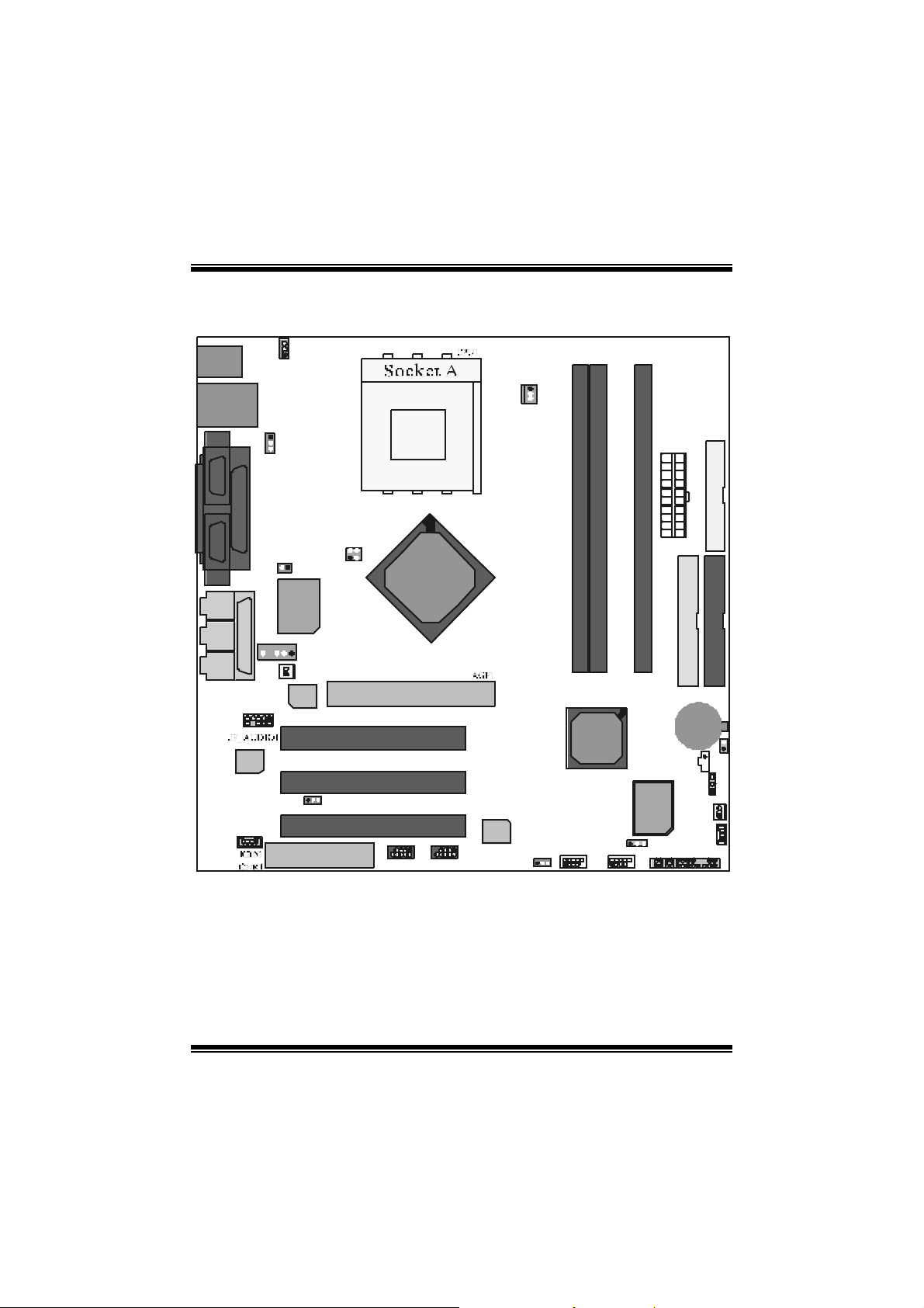
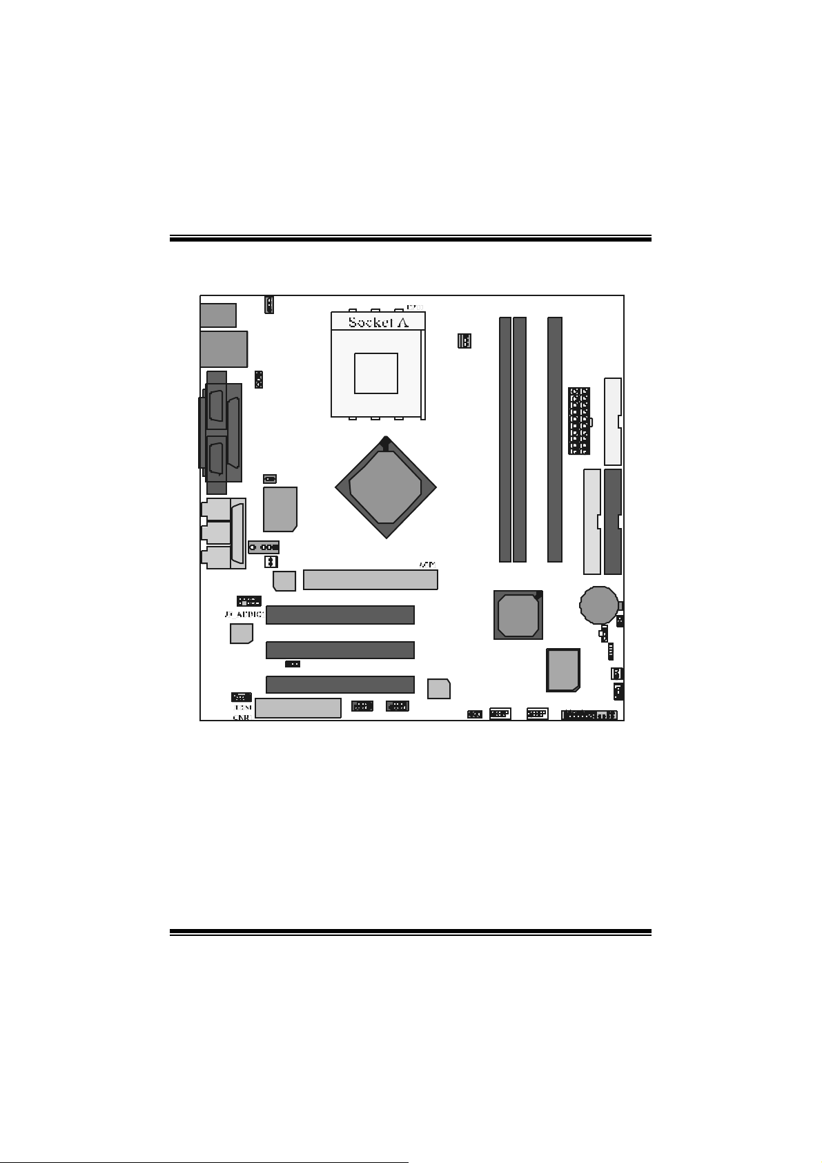
Layout of M 7NCG
b
b
b
D
d
r
a
o
D
d
r
a
o
i
r
c
s
e
r
c
s
e
n
o
i
t
p
n
o
i
t
p
i
n
o
i
t
p
i
r
c
s
e
D
d
r
a
o
JKBMS1
JSPKR1
SP - OU T
JLIN1
LINE-IN
JMIC1
MIC-IN
JCOM1
GAME Port
JGAME1
9
10
JUSBLAN1
1
JUSBV2
JPRNT1
1
1
2
1
JKBV1
1
1
JCLK3
JDJ1
JNFAN1
1
JTV1
24
1
3
J CODECSEL
IGP
PCI1
PCI2
PCI3
JUSBV 1
1
JUSBV41
2
1
J SPD IF1
JCMOS
JPAN EL1
1
FDD1
IDE1IDE2
1
JC1
24
1
3
Page 6
h
t
o
M
h
t
o
M
h
t
o
M
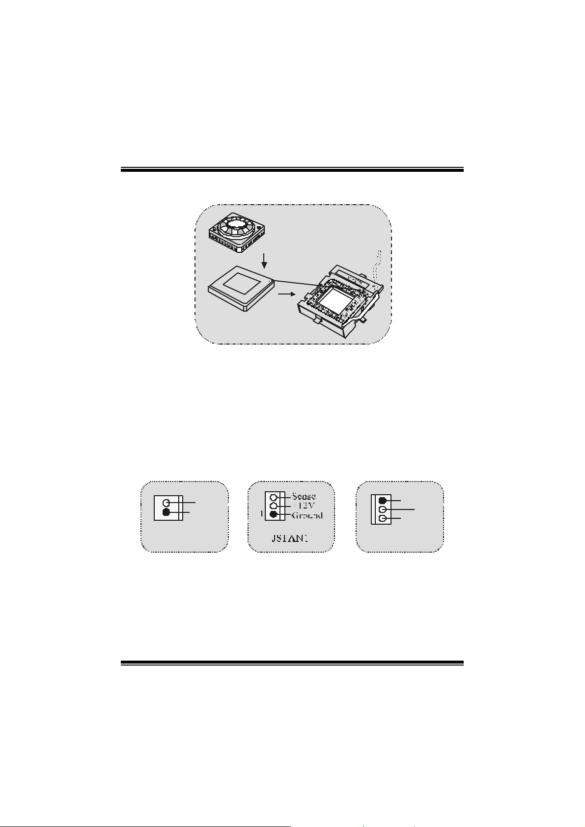
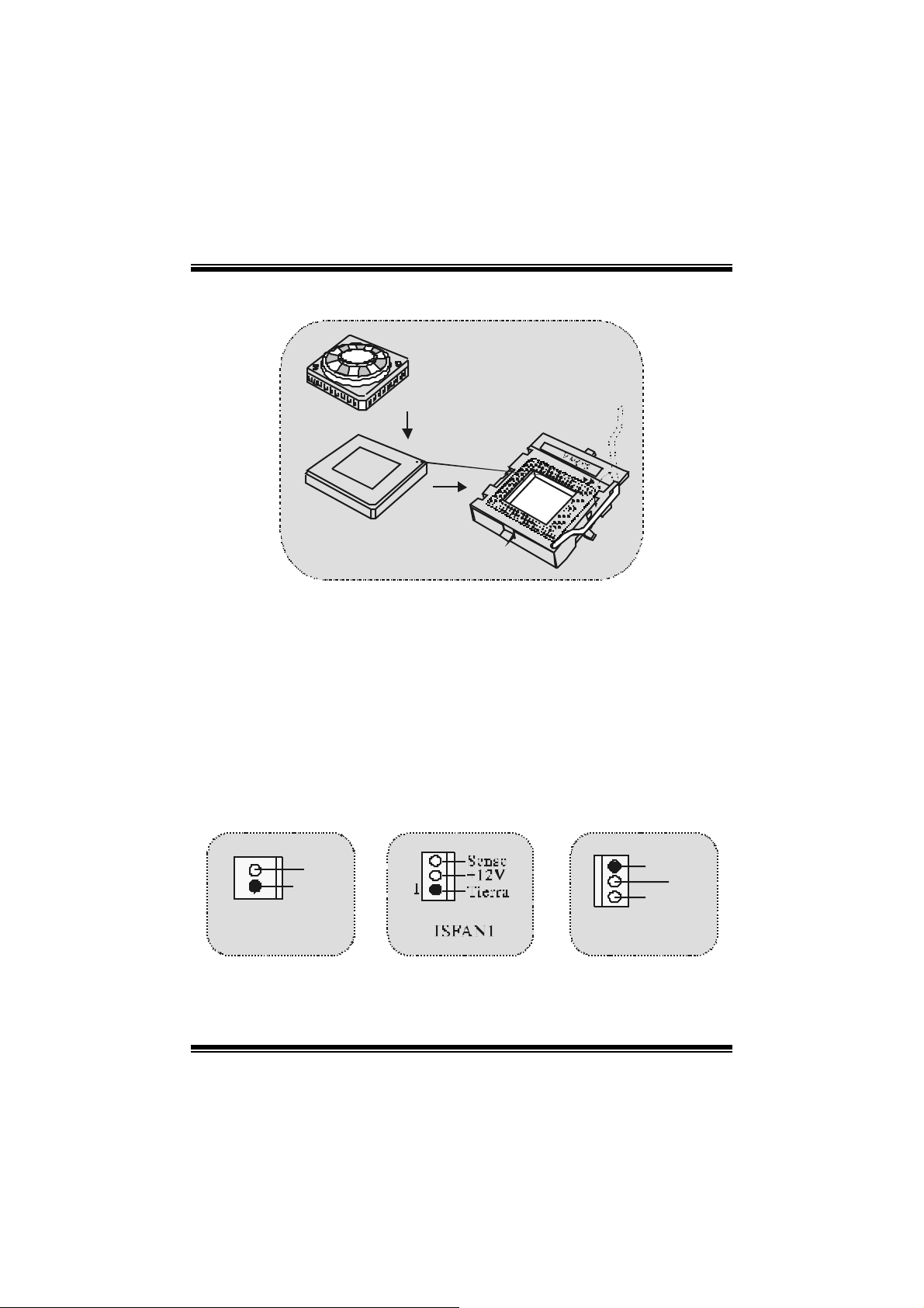
CPU Installat ion
e
b
r
e
b
r
e
D
d
r
a
o
D
d
r
a
o
i
r
c
s
e
r
c
s
e
n
o
i
t
p
n
o
i
t
p
i
n
o
i
t
p
i
r
c
s
e
D
d
r
a
o
b
r
1. Pull the lev er s ideways away f rom t he soc ket then raise the lever up to
90-degree angle.
2. Locat e Pin A in the socket and lock f or the whit e dot or c ut edge in t he CPU .
Match Pin A with the white dot/ c ut edge then insert the C PU.
3. Press the lever down. Then Put the f an on t he CPU and buckle it and put the
fan’s power port into the JCFAN1, then to c omple te the instal lation.
C
P
U
CPU/ System Fan Headers: JCFAN1/ JSFAN1/ JNFAN1
1
12V
Ground
JNFAN1
1
Ground
12V
Sen se
JCFAN1
4
Page 7
M
M
M
o
b
r
e
h
t
o
d
r
a
o
D
r
c
s
e
i
r
c
s
e
D
d
r
a
o
b
r
e
h
t
n
o
i
t
p
n
o
i
t
p
i
n
o
i
t
p
i
r
c
s
e
D
d
r
a
o
b
r
e
h
t
o
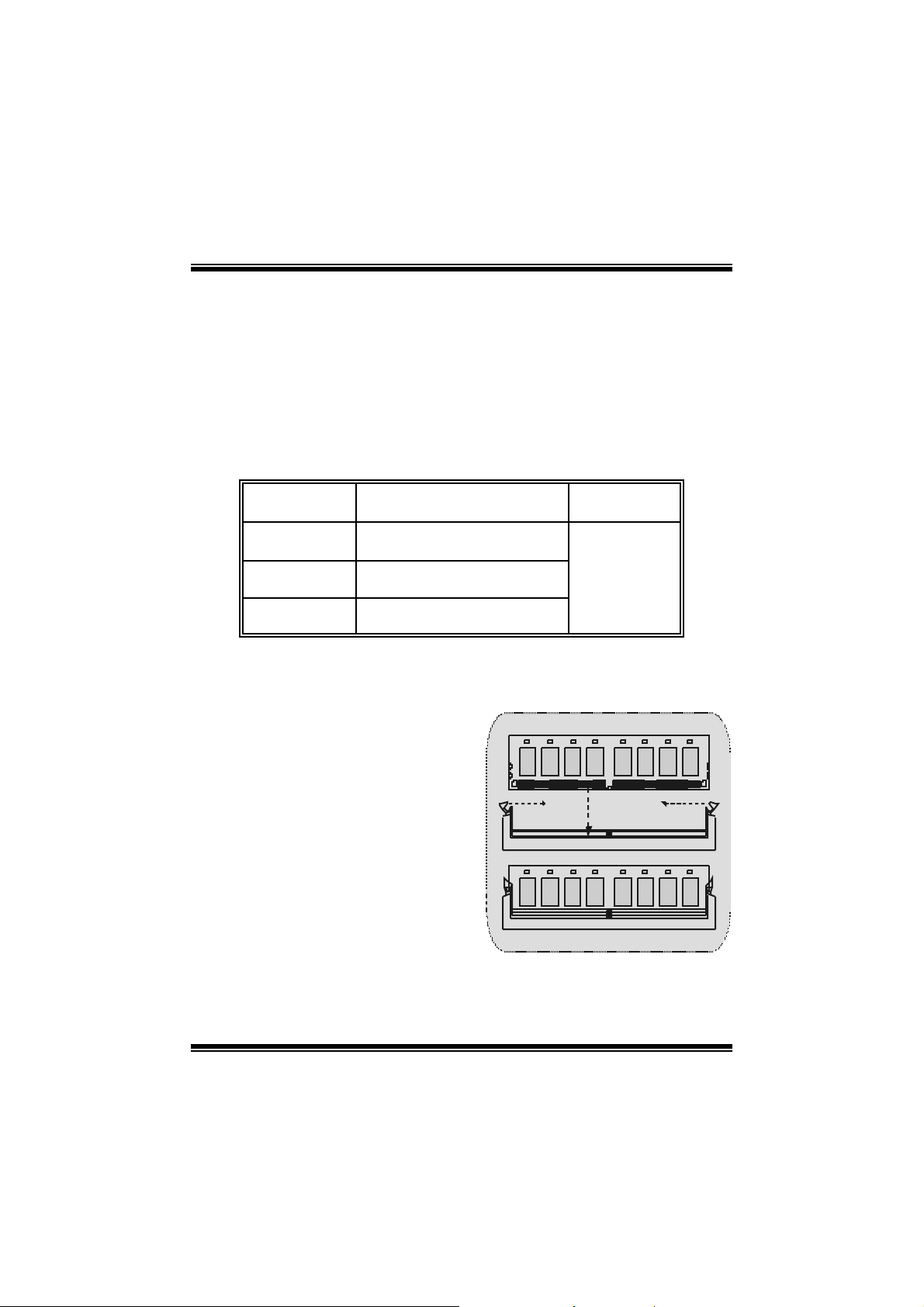
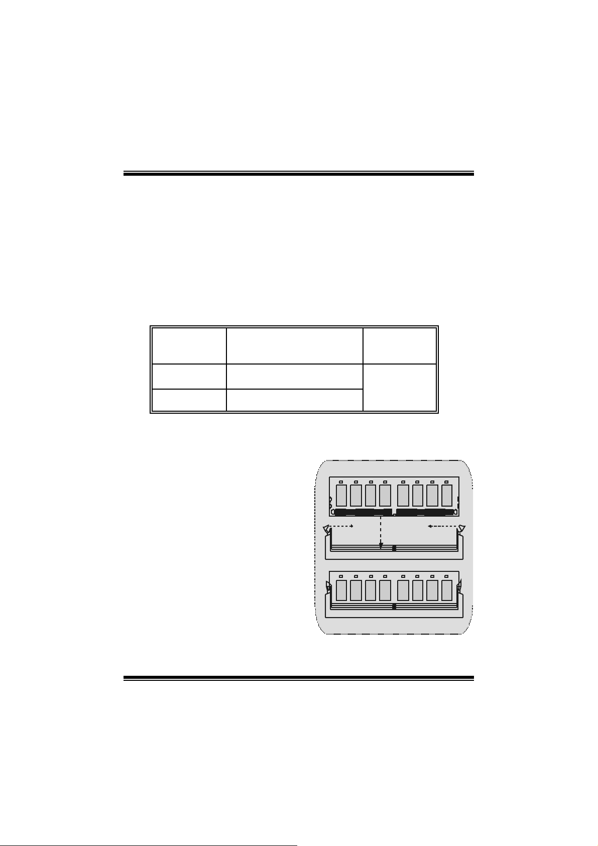
DD R DI M M Mo dules: D I MMB1 / D I M MB2/
DIMM A1
For Dual-channel DDR (128-bit) high performance, at least 2 or
more DIMM modules must be installed. (It has to be the
combination of DIMM A and DIMM B.) With only one DIMM i nsta lle d,
the memory performs only at 64-bit.
DRAM Access Tim e: 2. 5V Unbuffered DDR 200/266/ 333 MHz Type required.
DRAM Ty pe: 64MB/ 128MB/ 256MB/ 512MB/ 1GB DI MM Module (184 pin)
DIMM Socket
Location
DIMMB1 64MB/128MB/256MB/512MB/1GB
DIMMB2 64MB/128MB/256MB/512MB/1GB
DIMMA1 64MB/128MB/256MB/512MB/1GB
⌦The list s hown abov e for DRAM conf iguration is only for ref erence.
DDR Module Total Memory
Size (MB)
*1
Max i s
*1
*1
3GB
How to install a DIMM Module
1. The DIMM socket has a “ Plastic
Safety Tab”, and the DIMM memory
module has an “Asymmetrical notch”, so
the DIMM memory module can only fit
into the s lot in one direction.
2. Push the tabs out. Insert the DIMM
memory modules into the socket at a
90-degree angle, then push down
vertica lly so that it will f it into the place.
3. The Mounting Holes and plastic tabs
should fit over the edge and hold the
DI MM m emory m odules in place.
5
Page 8

M
M
M
o
b
r
e
h
t
o
d
r
a
o
D
r
c
s
e
i
r
c
s
e
D
d
r
a
o
b
r
e
h
t
n
o
i
t
p
n
o
i
t
p
i
n
o
i
t
p
i
r
c
s
e
D
d
r
a
o
b
r
e
h
t
o
Jumpers, Headers, Connectors & Slots
Hard Disk Connec tors: IDE1/ IDE2
The motherboard has a 32-bit Enhanced PCI IDE Controller that provides PIO
Mode 0~4, Bus Master, and Ultra D MA / 33/ 66/ 100/ 133 functionality. I t has two
HDD connec t ors IDE1 (primary) and IDE2 (secondary ).
The ID E connect ors can connect a master and a slave driv e, so you can c onnect
up t o f our hard disk drives. The first hard drive s hould alway s be connected t o
IDE1.
Floppy Disk Connector: FDD1
The motherboard provides a s tandard f loppy dis k c onnec tor t hat supports 360K,
720K, 1.2M, 1.44M and 2.88M floppy disk types. This connector supports the
prov ided f loppy drive ribbon cables.
Commun ication Netwo r k Riser Slot: CNR1
The CNR specification is an open Indust ry Standard Architecture, and it defines a
hardware scalable riser card int erface, which supports audio, network and m odem
only.
Peripheral Comp onent I nt erconnect Slots: P CI 1-3
This m ot herboard is equipped with 3 st andard PCI s lots. PCI stands for Peripheral
Component Int erc onnec t, and it is a bus st andard f or expansion cards , whic h has,
supplanted the older ISA bus st andard in most ports. This PCI slot is designated
as 32 bits.
AGP (Accelerated Graphics Port) Slot: AGP1
Your monitor will attach directly to that video card. This motherboard supports
video cards f or PCI slots, but it is also equipped with an Accelerated G raphics Port
(AGP). An AGP card will take advantage of AGP technology f or improved video
efficiency and perform ance, especially with 3D graphics.
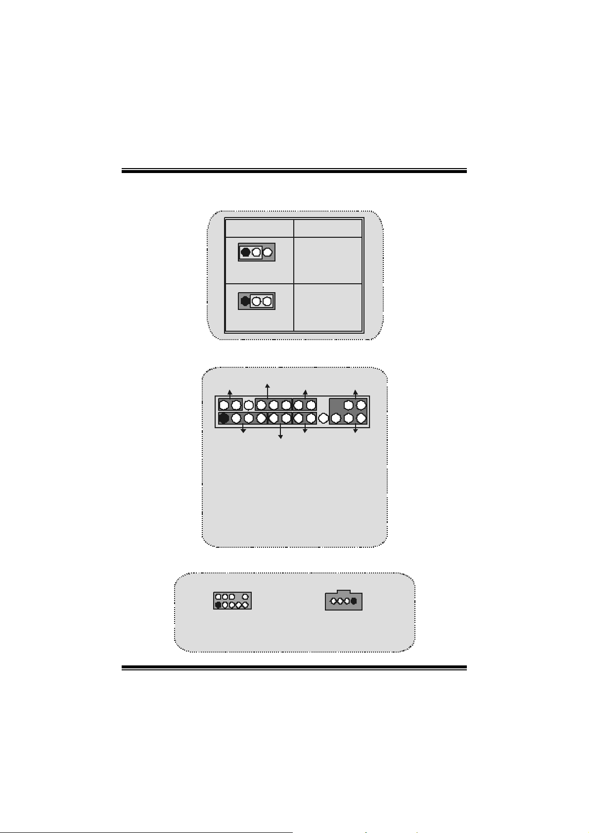
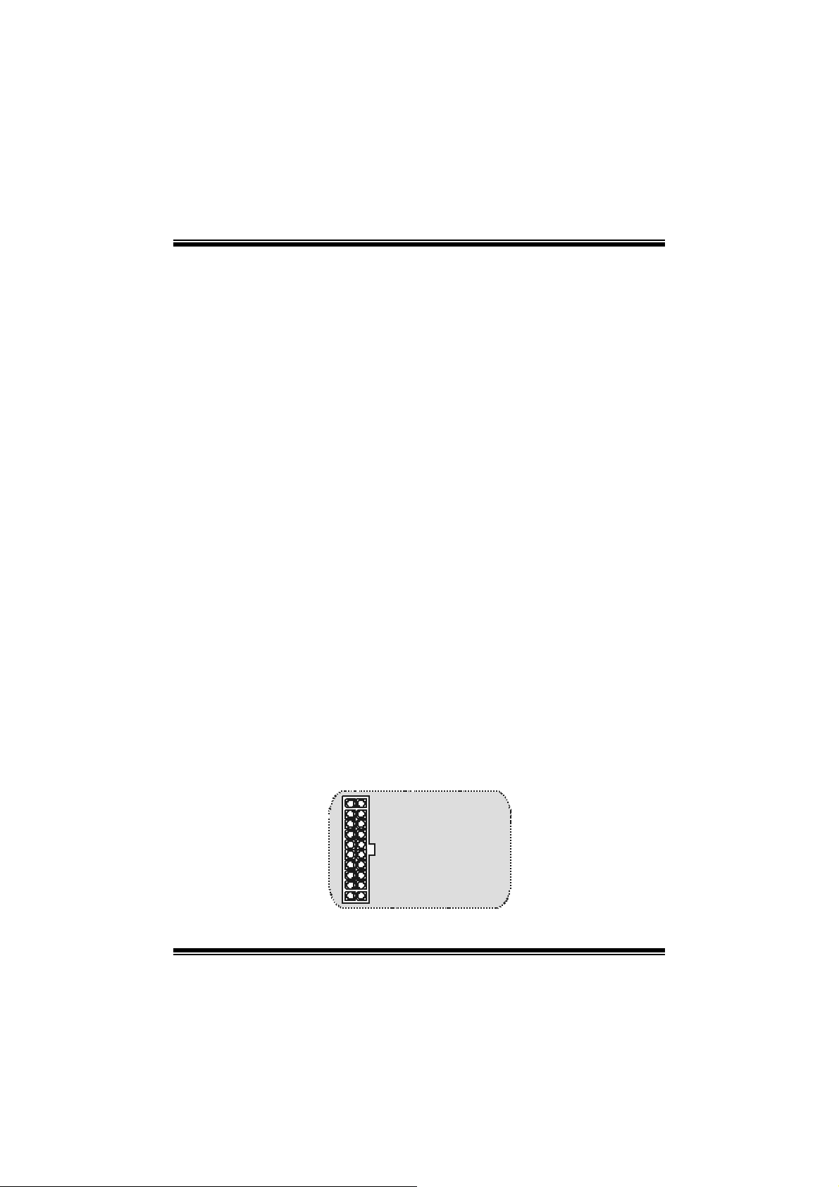
Power Connectors: JATXPWER1
JATXPWR1
( ATX Main Power Conn.)
JATXPWR1
( ATX Power Conn.)
6
Page 9
M
p
M
M
o
e
h
t
o
r
a
o
b
r
d
r
a
o
b
r
e
h
t
c
s
e
D
c
s
e
D
d
c
s
e
D
d
r
a
o
b
r
e
h
t
o
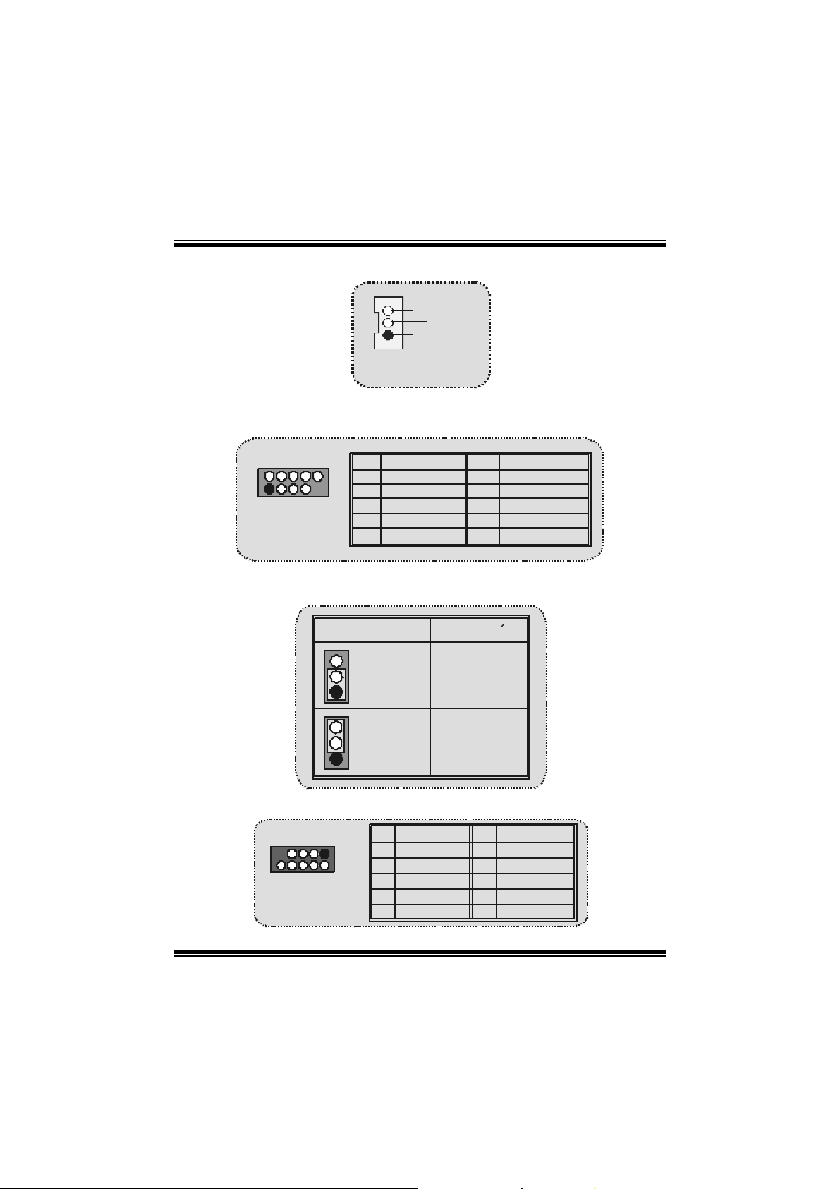
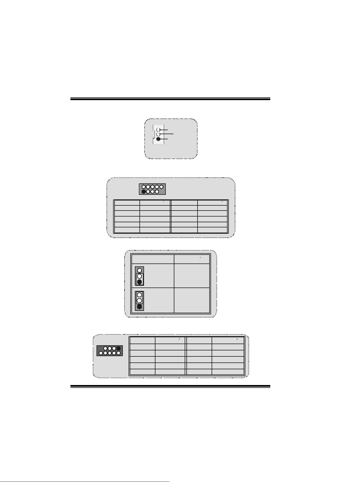
Wake On LAN Header: JWOL1
1
Wake u
Ground
5V_SB
JWOL1
Front USB Header: JUSB1/ JUSB2
2
1
JUSB 1 /2
Pin Assignment Pin Assignment
12
+5V +5 V
56
D ata (+ ) Data (+)
Ground Ground
910
Key NA
5V/ 5V_SB Selection for KB: JKBV1
JKBV1
Contactos
1-2 on
1
Contactos
2-3 on
1
Asignacion
5V_SB
Front 1394 Header: J1394A/ J1394B
J1394A/ B
Pin Assignment Pin Assignment
1
1
3
2
5
7
A+ A-
B+ B-
+1 2V +12V
9
r
r
r
5V
i
i
n
o
i
t
p
n
o
i
t
p
i
43
Da ta (-)D at a (-)
n
o
i
t
p
87
2
4
GroundGround
6
8
10
GNDKEY
7
Page 10
M
(
)
(
)
M
M
o
b
r
e
h
t
o
d
r
a
o
D
r
c
s
e
i
r
c
s
e
D
d
r
a
o
b
r
e
h
t
n
o
i
t
p
n
o
i
t
p
i
n
o
i
t
p
i
r
c
s
e
D
d
r
a
o
b
r
e
h
t
o
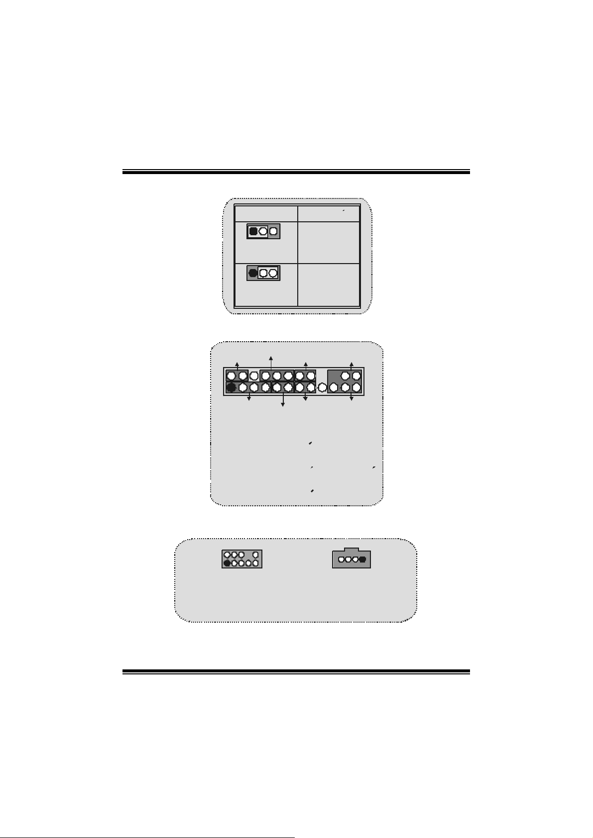
5V/ 5V_SB Selection for USB: JUSBV1/JUSBV2/
(JUSBV4=>optional)
JUSBV1/ 2
1
Pi n 1-2 on
1
Pi n 2-3 on
Assignment
5V
5V_SB
Front Panel Connector: JPANEL1
SLP
2
1
SPK ==> Speaker Conn.
HLED ==> Hard Driver LED
RST ==> Reset Button
IR ==> Infrared Conn.
SLP = => Sleep Button
PWR_LED ==> Power LED
O N/ OFF ==> Power-on Bu tton
SPK
PWR_LED
(+) (-)(+)
(+) (-)
HLED
RST
IRON/OFF
24
23
IR
Audio Subsys tem: JF_AUDIO1/ JCDIN1
2
2
1
1
JA UDIO1
JF_AUDIO1
(F ront Audio He a de r )
(F ront Audio He a de r )
1
1
JCDIN1
CD-ROM Audio-In Header
CD-ROM Audio-In Header
JCDIN1
8
Page 11
M
e
h
t
o
M
e
h
t
o
M
⌦ JF_AUDIO1 only support 2CH.
12
3
5
7
910
12
3
5
7
910
2
2
1
Pin
1
3
5
7
9
Jumper Setting Configuration
4
6
4
6
Assignment
Mic In
Mi c Po wer
RT Line Out
Reserved
LFT Line Out
Front Panel Audio Conne ctor/ Jumper Block
Pin 5 and 6
Pin 9 and 10
No jumper s
installed
d
r
a
o
b
r
d
r
a
o
b
r
10
9
Audio line out sign als are routed
to the back panel audio line out connector.
Audio line out and mic in signals are
ava il able for front panel aud io connectors.
d
r
a
o
b
r
e
h
t
o
D
D
r
c
s
e
r
c
s
e
r
c
s
e
D
JF_AUDIO1
Pin
2
4
6
8
10
i
i
n
o
i
t
p
n
o
i
t
p
i
Assignment
Gro und
A u dio Powe r
RT L ine O ut
Key
LFT Line Out
n
o
i
t
p
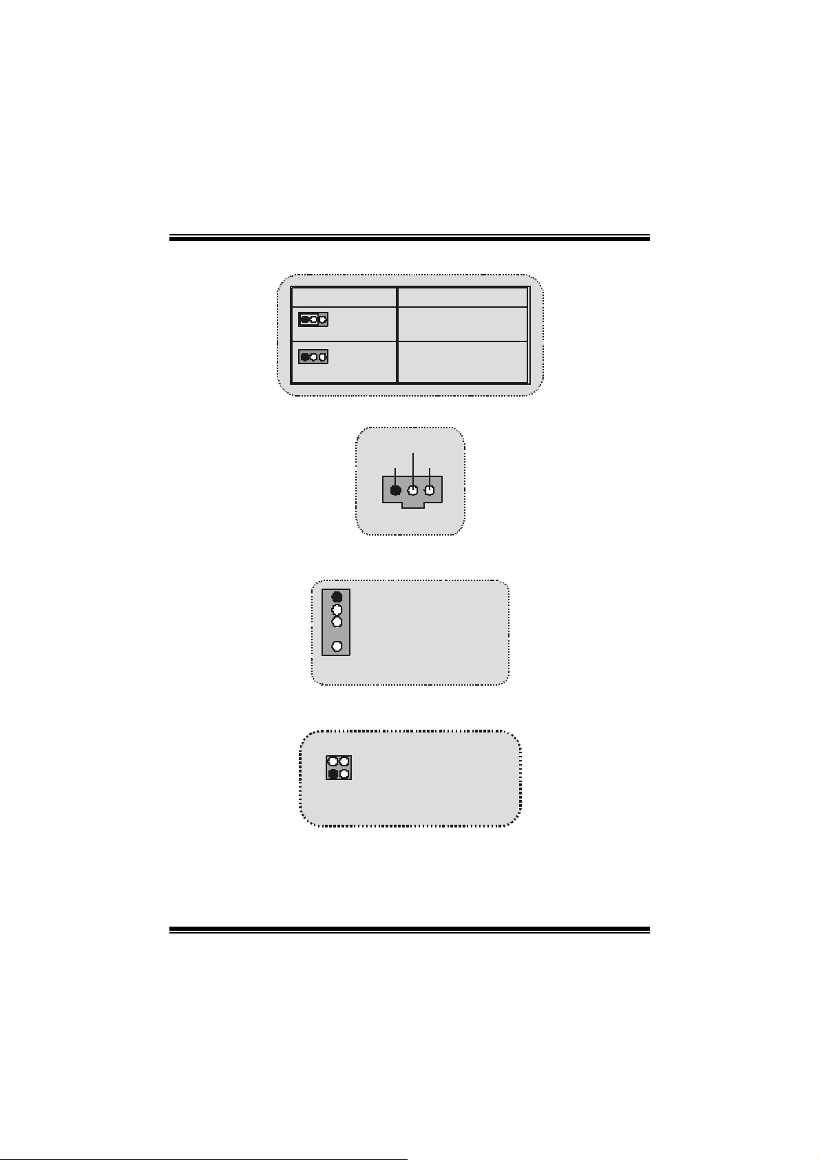
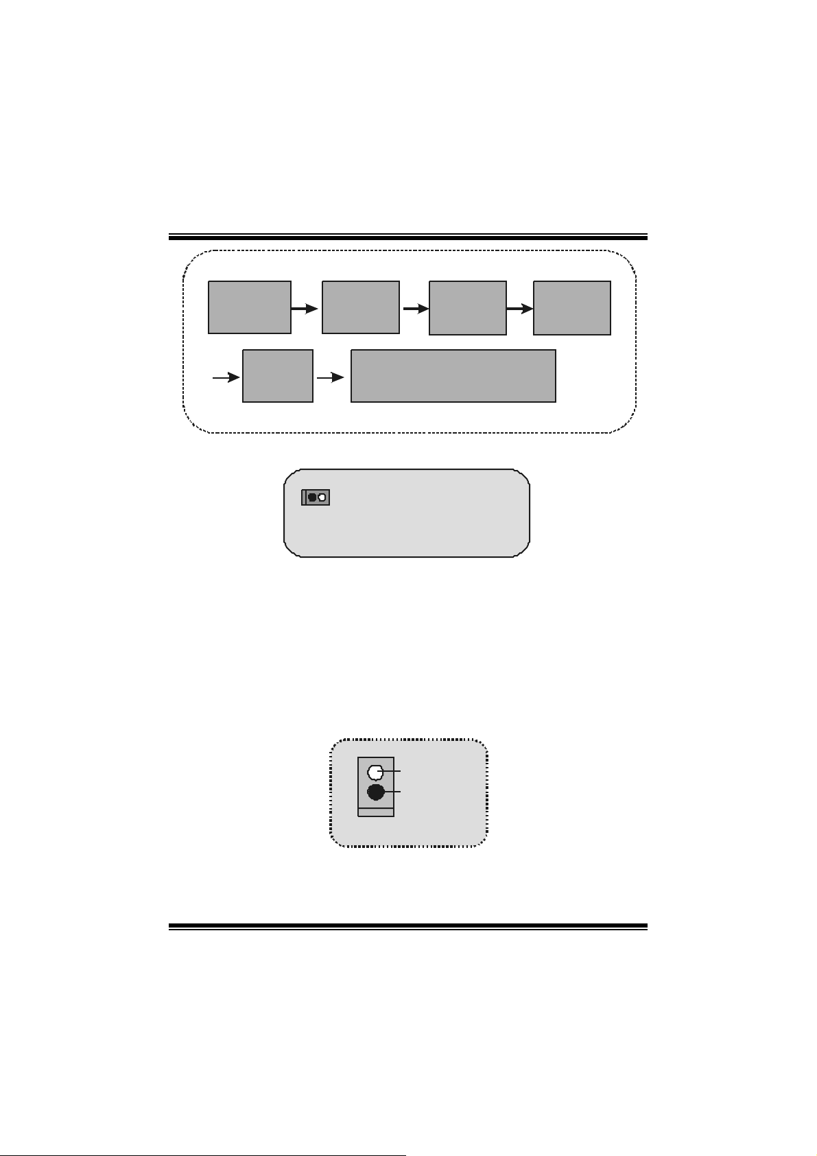
Clear CMOS Jumper: JCMOS
JCMOS
Pi n 1-2 on
1
Pi n 2-3 on
1
Assignment
Norm al
Operation
(default)
Clea r CMOS
Data
9
Page 12
M
)
M
M
o
b
r
e
h
t
o
b
r
e
h
t
o
D
d
r
a
o
D
d
r
a
o
i
r
c
s
e
r
c
s
e
n
o
i
t
p
n
o
i
t
p
i
n
o
i
t
p
i
r
c
s
e
D
d
r
a
o
b
r
e
h
t
Remove AC
p ower line
AC power
on
JCMOS1
Pin2-3 close
Reset the passwort as your will
or clea r CMOS data
wait 15
seconds
JCMOS
Pi n1-2 clo se
Freq uency Sel ec t ion: J C L K 3
Note: W hen ov erclock f unction failed and system is unable to boot-up, please
foll ow the in structio n below:
1. T u r n off the system.
2 . Closed the JCLK3 jumper .
3. Turn on the syst em.
4. Enter CMOS set up menu and load def aults settings .
5. T u r n off the system.
6. Open t he JCLK3 jumper.
7. Turn on the syst em.
1
JCLK3
Op en == >
(
C l os e ==> Safe Mode
(100MHz )
Us er Mod e (d efau lt)
133/166MHz
Ca se Op e n Connect or : J C1
Case O pe n
Signal
Ground1
JC 1
10
Page 13
M
y
y
M
M
o
b
r
e
h
t
o
d
r
a
o
D
r
c
s
e
i
r
c
s
e
D
d
r
a
o
b
r
e
h
t
n
o
i
t
p
n
o
i
t
p
i
n
o
i
t
p
i
r
c
s
e
D
d
r
a
o
b
r
e
h
t
o
CNR Codec Primary/Secondary Selection: J_CODECSEL
J_CODECSEL
Pin 1- 2 On-b oard Pr imar
Codec.
1
Pin 2- 3 CNR Primar
1
Assig nment
Codec.
Digital Audio Connector: J_SPDIF1
SPDIF_ OUT
GNDVCC5
1
J_SPD IF1
Audio D J Header: JD J1 (only supports version 3.0)
15Pin 1 ==> SM BDT
Pin 2 ==> SM BCK
Pin 3 ==> -I N T R_B
Pin 4 ==> Ke y
JDJ1
Pin 5 ==> PWRGD
T V Out Header : JTV 1 (only supports with version 3 .0)
24
1
JTV1
Pin1 ==> TV_Y
Pin2 ==> Ground
3
Pin3 ==> Ground
Pin4 ==> TV_C
11
Page 14
e
h
t
o
M
e
h
t
o
M
e
h
t
o
M
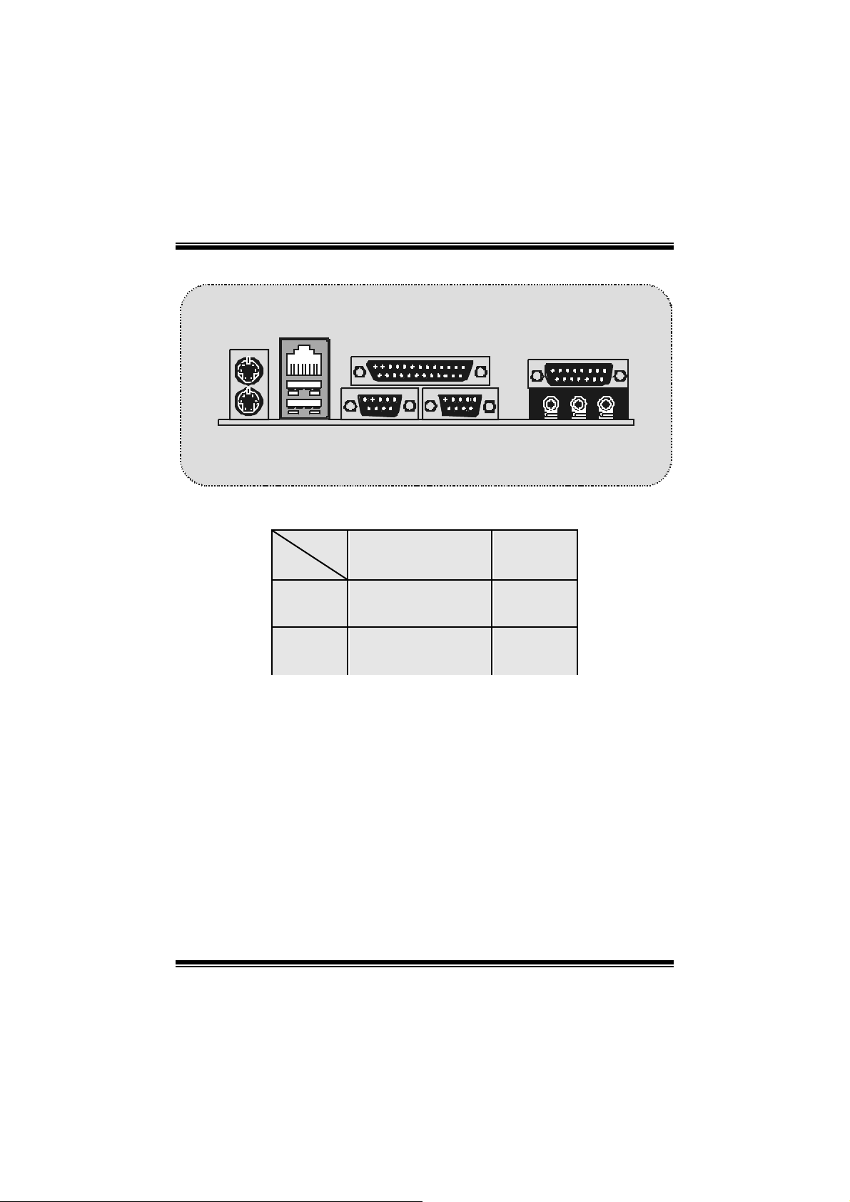
B ack Pa nel Connectors
r
b
r
b
r
D
d
r
a
o
D
d
r
a
o
i
r
c
s
e
r
c
s
e
n
o
i
t
p
n
o
i
t
p
i
n
o
i
t
p
i
r
c
s
e
D
d
r
a
o
b
JKBMS1
PS/2
Mouse
PS/2
Keyboard
JUSBLAN1
LAN(Optional )
USB
COM1
JCOM1
JPRNT1 JGAME1
Parallel
COM2
JCOM2
The LED indicator for Lan port status:
Status
Speed
10M bps
100M bps
Normal Download
Righ t li gh t: gr een
Left light: no
Righ t li gh t: gr een
Left light: orange
Gam e Po rt
Speaker
Out
Light: blink
Light: blink
Li ne In
Mic
In
12
Page 15

M
M
M
b
r
e
h
t
o
b
r
e
h
t
o
d
r
a
o
d
r
a
o
d
r
a
o
b
r
e
h
t
o
Español
Características del M7NCG
D
D
D
i
r
c
s
e
r
c
s
e
n
o
i
t
p
n
o
i
t
p
i
n
o
i
t
p
i
r
c
s
e
CPU
- Soport a proc esador AMD
- Corriendo a 200/ 266/ 333MHz F SB.
Chipset
- Nort h Bridge: nFORC E2 C rus h18G IGP Chips et.
- South Bridge: MC P- T C h i pse t.
High Speed 800Mb/s Hy per-Transport interf ace para el
MCP-T.
Memo r ia Principal
- S o p ort a ha sta 3 di sp osit ivo s DDR.
- Soport o 200/ 266/333MH z (sin ECC) dis posit ivos DDR.
- High performanc e 128-bit DD R 333 Twin Bank Mem ory Architect ure.
- Capacidad m áxim a de m emoria es 3GB.
Ranuras
- Tres ranuras de 32-bit PCI bus master.
- Una ranura CNR.
- Una ranura AGP: AGP3.0 8X interface a 533M b/s.
Soporta AGP 4X, 8X.
On Board IDE
- Soport a c uatro disc os IDE.
- Soport a Modo 4 PIO, Modo Master y Ult ra DMA 33/ 66/100/133 Bus Modo
Master.
On Bo ard VGA
- GeForce 4MX Series Unidad Gráfic os de Proceso (GPU).
Chi p 1394
- Realtek 8801BL.
- Soport a 2 puertos con transf erencia de hasta 400Mbps.
Audio
- I n t e rf ace AC 97 2.2 .
- PC99 complaint.
- Soports 6 canales.
- S/PDIF Out.
TV Ou t (solam ente p ara versi ón 3.0)
- Soport a m odo s-video output.
®
Zóc alo 462 de hast a XP 3000+.
13
Page 16

M
M
M
- Res olución de pant alla de has ta 1024 x 768 (incluy endo todos los modos
DOS)
- Soport a f ormatos de TV: NTSC-M (Am érica del Norte y Taiwan)
NTSC-J (Japón)
PAL (Europa y Asia)
Per i féricos On Bo ard
- Soport a 360K, 720K, 1. 2MB, 1.44MB y 2.88MB unidad de disquete
- Soport a 2 puertos serie.
- Soport a 1 mult i-modo del puerto paralelo (modos SPP/EPP/EC P)
- Soport a rat ón PS/ 2 y t eclado PS/2.
- Soport a 2 puertos USB2.0 traseros y 4 puertos USB2. 0 delanteros.
- Soport a c onector S/ PDIF Out.
BIOS
- AWARD legal Bios .
- Soporta APM1.2.
- Soporta ACPI.
- Sopo rta fun ció n USB.
Sistemas Operativos
- Ofrece alto rendimiento en MS-DOS, Windows 2000, Windows Me,
Windows XP, SC O UNIX etc.
Dimensión
- Fac t or de Forma Micro ATX: 24.4c m X 24. 4cm (W X L)
b
r
e
h
t
o
b
r
e
h
t
o
D
d
r
a
o
D
d
r
a
o
i
r
c
s
e
r
c
s
e
n
o
i
t
p
n
o
i
t
p
i
n
o
i
t
p
i
r
c
s
e
D
d
r
a
o
b
r
e
h
t
o
Contenido del Pa quete
- Cable HD D X 1
- Cable FD D X 1
- Configuración Completa del D river CD X 1
- Manual del Usuario X 1
- Cable USB X 2 (Opcional)
- Cable SPDI F OU T X1 (Opc ional)
- Cable IEEE 1394 X1
14
Page 17
M
_
_
M
M
e
h
t
o
e
h
t
o
d
r
a
o
b
r
d
r
a
o
b
r
d
r
a
o
b
r
e
h
t
o
D is po s i ción de l M 7N C G
D
D
i
r
c
s
e
r
c
s
e
n
o
i
t
p
n
o
i
t
p
i
n
o
i
t
p
i
r
c
s
e
D
JKBMS1
JSPKR1
SP-OUT
JL I N1
LI NE-I N
JMIC1
MIC-IN
JCOM1
JVGA1
GA ME Po r t
J GAM E 1
9
10
Codec
JUSBLAN1
1
JUSBV2
JPRNT1
1
Winbond
1
1
2
1
JKBV1
1
JCLK3
I/O
15
JDJ 1
JNFAN1
Lan
Chi p
1
J
CODECSEL
9101
IGP
9101
2
J1394B
PCI1
PCI2
PCI3
1
JCFAN1
FD D1
JATX PW ER1
DIMMB1
MCP-T
1394A
Chi p
2
JUSBV1
1
2
1
JUSB1
10
9
DIMMB2
JUSB 2
2910
1J1394A
DIM MA1
BIOS
2
1
J
SPDIF1
JCM OS
JPAN EL1
BAT1
1
JSFAN1
JW OL1
IDE1IDE2
1
JC1
1
1
1
24
23
15
Page 18
M
M
M
r
e
h
t
o
r
e
h
t
o
r
e
h
t
o
Instalac ión de la CPU
b
b
b
D
d
r
a
o
D
d
r
a
o
i
r
c
s
e
r
c
s
e
n
o
i
t
p
n
o
i
t
p
i
n
o
i
t
p
i
r
c
s
e
D
d
r
a
o
1. Tire de la palanca del lado del zócalo, luego levante la palanca hasta un
ángulo de 90 grados.
2. Sitúe el cont acto A del zócalo y bus que el punto blanco o corte el borde en la
CPU . Em pareje el c ontacto A con el punto blanco/ corte del borde, luego
inse rte la C PU.
3. Presione la palanc a para abajo. Ponga el v entilador en la CPU y abróc helo.
Luego ponga el puerto de corriente del vent ilador en el JC F AN1. Y ya habrá
com pletado s u instalación.
C
P
U
CPU/ Cabezal del Sistema de Ventilación: JCFAN1/ JSFAN1/
JNFAN1
12V
1
Tierra
1
Tierra
12V
Sen s e
JNFAN1
16
JCFAN1
Page 19
M
M
M
o
b
r
e
h
t
o
d
r
a
o
D
r
c
s
e
i
r
c
s
e
D
d
r
a
o
b
r
e
h
t
n
o
i
t
p
n
o
i
t
p
i
n
o
i
t
p
i
r
c
s
e
D
d
r
a
o
b
r
e
h
t
o
Módulos DDR DIMM: DIMMB1/DIMMB2/
DIMM A1
Para un alto funcionamiento, Dual-channel DDR (128-bit), por
lo menos 2 o más módul os DIM M debe ser instalado. (Ti ene
que ser la combinación del DIMMA y DIMMB.) Con solamente
un DIMM instal a do, la memo ri a funcion a s o lament e a 64- b i t.
DRAM Tiempo de Acceso: 2.5V Unbuffered DDR 200/266/333 MHz Tipo
requerido.
DRAM Tipo: 64MB/ 128MB/ 256MB/ 512MB/ 1GB Módulos DIMM (184 c ontac t os)
Loca lización
del Zócalo
DIMM
DIMMB1 64MB/128MB/256MB/512MB/1GB
DIMMB2 64MB/128MB/256MB/512MB/1GB
⌦La lis t a de arriba para la configuración DR AM es solamente para ref erencia.
M ódul o DDR Tota l del
Tamaño de
Me m o r ia (MB)
*1
*1
Máxi m o 3G B
Cómo instalar un módulo DIMM
1. El zócalo DIMM tiene una lengüeta
plástica de seguridad y el módulo de
memoria DIMM tiene una muesca
asimétrica, así el módulo de memoria
DIMM puede caber solamente en la
ranura de una sóla direcc ión.
2. Tire la lengüeta hacia afuera. Inserte
los módulos de memoria DIMM en el
zócalo a los 90 grados, luego empuje
hacia abajo v erticalmente de modo que
encaje en el lugar.
3. Los agujeros de montaje y las
lengüetas plásticas deben caber por
sobre el borde y sostenga los módulos
de memoria DIMM en el lugar.
17
Page 20
M
M
M
o
b
r
e
h
t
o
d
r
a
o
D
r
c
s
e
i
r
c
s
e
D
d
r
a
o
b
r
e
h
t
n
o
i
t
p
n
o
i
t
p
i
n
o
i
t
p
i
r
c
s
e
D
d
r
a
o
b
r
e
h
t
o
Conectores, Cabezales, Puentes y Ranuras
Conectores del Disco Duro: IDE1/ IDE2
La plac a madre tiene un controlador de 32-bit PCI ID E que proporc iona Modo PIO
0~4, Bus Master, y func ionalida Ultra D MA / 33/ 66/ 100. Tiene dos conect ores
HD D IDE1 (pr i mario ) y IDE2 (se cundario).
El conector IDE puede conectar a un master y un drive esclavo, así puede
conectar hasta cuatro discos rígidos. El primer disc o duro debe es tar siem pre
conectado al IDE1.
C on ector para el Disquete: FDD1
La plac a madre proporciona un conect or estándar del dis quete (FDC ) que soporta
360K, 720K, 1.2M, 1.44M y 2.88M tipos de disquete. Éste conector utiliza los
cables de cint a proporcionados por el disquete.
Ranur a de Banda de Suspensión de Comunicación y Red: CNR1
La es pec ific ación CNR es una abierta Industria Est ándar de Arquitect ura, y define
una tarjeta hardware escalable de interface en el que soporta audio, red y
módem.
Ranura de Intercone xión del Componente Peri férico: PCI1-3
Ésta placa madre está equipado con 3 ranuras PCI. PCI es la sigla para
Interconexión del Componente Periféric o, y es un est ándar bus para la tarjeta de
expansión en el que reemplaza, en s u may oría de las part es, al antiguo estándar
ISA bus. Las ranuras de PCI est án desiñados c on 32 bit s.
Ranu ra del Puerto Acelerado para Gráficos: AGP1
Su m onitor s e fijará directamente a la tarjet a de video. Ésta placa m adre soport a
tarjetas de video para ranuras PCI, y también está equipado con un Puerto
Acelerado para Gráficos (AGP/ solamente soporta 1.5V y 4X tarjeta AGP). Ésta
tarjeta AGP t omará vent aja de la tecnologí a del AGP para el mejoram iento de la
eficiencia y fun cionamien to del video , e special m ente con gráfi cos 3D.
Conector de Corriente: JATXPWER1
JATXPWR 1
(Conector de
Corriente ATX)
18
Page 21
M
p
M
M
o
b
r
e
h
t
o
D
d
r
a
o
D
d
r
a
o
b
r
e
h
t
p
i
r
c
s
e
i
r
c
s
e
p
i
r
c
s
e
D
d
r
a
o
b
r
e
h
t
o
Cabezal Wake On LAN: JWOL1
1
Wake u
Tierra
5V _SB
JWOL1
Cabez al Frontal USB: JUSB1/ JUSB 2
Contactos Asignacion Contactos Asignacion
2
1
12
56
910
Data (+) Data (+)
Tierra Tierra
JUSB1/2
+5V +5V
43
87
Key NA
5V/ 5V_SB Selecci ón para KB: JKBV1
JKBV1
Contactos
1-2 on
1
Contactos
2-3 on
1
Asignacion
5V
5V_SB
Cabez al Frontal 1394: J1394A/ J1394B
J1394A/ B
Contactos Asignacion Contactos Asignacion
1
1
3
2
5
7
A+ A-
B+ B-
+12V +12V
9
p
t
t
t
2
4
6
8
10
n
o
i
n
o
i
n
o
i
Data (-)Data ( -)
TierraTierra
GNDKEY
19
Page 22
M
j
(
M
M
o
b
r
e
h
t
o
d
r
a
o
D
r
c
s
e
i
r
c
s
e
D
d
r
a
o
b
r
e
h
t
n
o
i
t
p
n
o
i
t
p
i
n
o
i
t
p
i
r
c
s
e
D
d
r
a
o
b
r
e
h
t
o
5V/ 5V_SB Selecci ón para USB: JUSBV1/JUSBV2
JUSBV1/ 2
1
Contactos
1-2 on
1
Contactos
2-3 on
Asi gnacion
5V
5V_SB
Conector del Panel Frontal: JPANEL1
2
123
SPK ==> Conector de Altavoz
HLED ==> LED del Disco Duro
RST ==> Boton de Reinicio
IR ==> Conector Infr aro
SLP ==> Boton de Suspension
PWR_LED ==> Corriente LED
ON/ OF F ==> Boton de Encendido
SLP
SPK
PWR_LED
(+) (-)(+)
(+) (-)
HLE D
RST
IRON/OFF
24
IR
o
Subs istema de Audio: JF_AUDIO1 / JCDIN1
(Cabezal de Audio Frontal)
2
1
JF_AUDIO1
1
JCDIN1
Cabezal de Entrada de
Audio CD-ROM)
20
Page 23
M
M
M
o
b
r
e
h
t
o
b
r
e
h
t
o
D
d
r
a
o
D
d
r
a
o
i
r
c
s
e
r
c
s
e
n
o
i
t
p
n
o
i
t
p
i
n
o
i
t
p
i
r
c
s
e
D
d
r
a
o
b
r
e
h
t
2
2
1
Contactos
1
3
5
7
9
⌦JF_AUDIO1 only support 2CH.
Conector del Panel Fr ontal de Audio/ Jumper Block
Ju mper Setting Configuracion
12
4
3
5
7
910
12
3
5
7
910
Contac to 5 & 6
6
Contacto 9 & 10
4
6
Asignacion
Entr ada del MI C
Corriente del MIC
RT S alida de Linea
Reservado
LFT Salida de Linea
No jumpers
insta lled
10
9
La senal de salida de linea del Audi o
encamina al conector de la salida de linea
del Audio ubicad o en el panel tra sero.
La senal de salida de linea del Audi o y la
~
senal del e nt rada del mic estan disponibles
desde el conector de Audio del
panel frontal.
J F_AUDIO1
Contactos
2
4
6
8
10
~
~
Asignacion
Tierra
Corriente de Audio
R T Salid a d e Lin ea
Key
LFT Sal ida de Linea
Clear CMOS Jumper: JCMOS
JCMOS
Contacto
1-2 on
1
Contacto
2-3 on
1
Asignacion
Operacion
Normal
(default)
Borrar Dat os
CMOS
21
Page 24
M
M
M
o
b
r
e
h
t
o
b
r
e
h
t
o
D
d
r
a
o
D
d
r
a
o
i
r
c
s
e
r
c
s
e
n
o
i
t
p
n
o
i
t
p
i
n
o
i
t
p
i
r
c
s
e
D
d
r
a
o
b
r
e
h
t
Quite el cable
de co rrie nte
del AC
Encienda
AC
JCMOS1
Cont actos
2-3 cerrado
Rec onfigure la con tra s ena
desea da o borre datos CMOS
Es p ere 15
segundos
JCMOS
Contac tos
1-2 cerrado
~
S elección de Frecu encia: JCLK3
Nota: C uando la función del overclock f alla y el s istema no pueda encenderse,
por fav or sig a la s sigi e nte s i nst r ucci o nes:
1. Apague el sistema.
2. I nserte el puente JCLK3 en cerrado.
3. Prenda el sistema.
4. Entre al menu de la configurac ión del CMOS y cargue las configuraciones
defaults.
5. Apague el sistema.
6. I nserte el puente JCLK3 en abiert o.
7. Prenda el sistema.
1
JCLK3
Abierto ==>
(
Cerrado == > Modo Seguro
(100MHz)
Use r Mod e (d efau l t )
133/166MHz)
Conector de l a Ca rcasa Abierta: JC1
1
~
Se nal de l
Case O pe n
Tierra
JC 1
22
Page 25

M
M
M
o
b
r
e
h
t
o
d
r
a
o
D
r
c
s
e
i
r
c
s
e
D
d
r
a
o
b
r
e
h
t
n
o
i
t
p
n
o
i
t
p
i
n
o
i
t
p
i
r
c
s
e
D
d
r
a
o
b
r
e
h
t
o
S elección CNR Codec Primario/ Secunda rio: J_ CODECSEL
J_CO DECSEL
Contacto
1
1
1-2
Contacto
2-3
Asignacion
Codec Prima rio
integrado en la placa madre.
CNR Codec Primario.
Conector Digital de Audio: J_SPDIF1
SPDIF_OUT
GNDVCC5
1
J_SPD IF1
Conectores del Panel Trasero
Raton
PS/2
Teclado
PS/2
JUSBLAN1
LAN
(Opcional)
USB
JPRNT1 JAUD_GAME
Puerto Paralelo
COM1
JCOM1
VGA1
JVGA1
23
Puerto de Juego
Salida del
Altavoz
Entrada
de Lin ea
Ent rada de
Mic
JKBMS1
Page 26

M
M
M
Estado del I ndi cador LED del LAN:
Estado
Velocidad
10Mbps
100Mbps
Indicador Derecho: Verde
Indicador Iz quierdo: Nada
Indicador Derecho: Verde
Indicador Iz quierdo: Naran ja
b
r
e
h
t
o
b
r
e
h
t
o
Normal Bajando D atos
D
d
r
a
o
D
d
r
a
o
D
d
r
a
o
b
r
e
h
t
o
e
i
r
c
s
e
r
c
s
e
n
o
i
t
p
n
o
i
t
p
i
Luz: Parpadeando
Luz: Parpadeando
n
o
i
t
p
i
r
c
s
24
Page 27

M
M
M
o
b
r
e
h
t
o
d
r
a
o
D
r
c
s
e
i
r
c
s
e
D
d
r
a
o
b
r
e
h
t
n
o
i
t
p
n
o
i
t
p
i
n
o
i
t
p
i
r
c
s
e
D
d
r
a
o
b
r
e
h
t
o
Deutsch
M7NCG Features
CPU
- Unt erst üt zung für AMD Prozessor(Sock el462 ) bis zu XP 3000+.
- FSB mit 200/266MHz..
Chipsatz
- Nort hbridge: nFORC E2 Crush 18G IGP Chipsat z.
- Southbridge: MCP-T.
800Mb/ s Hohe Geschwindigkeit : Hyper-Trans port
-Int erface zu den MCP-T C hipsatz.
Hauptspeicher
- Un t erstü t zu n g f ü r 3 DDR Ge rä te.
- Unt erst üt zung für 200/266/ 333MH z(ohne ECC ) DDR Ge r äte.
- 128-bit H igh-Perf orm ance DDR333 m it der Twin- Bank Architektur.
- Die maximale Speicher größe ist 3GB.
Slots
- Dre i 32-Bit PCI -Bus-Slots.
- Ein CNR-Slot.
- Ein AGP-Slot: AGP3.0 8X Interf ac e mit 533Mb/s.
U nt erst ützung f ür AGP 4X, 8X.
On Board IDE
- Unte rstützung für vier IDE Di skettenlauf wer ke.
- Unterstützung für PIO Modus 4, Master Modus und Ultra DMA
33/66/100/133 Bus Master Modus.
On Bo ard VGA
- GeForce 4MX Series graphic s proc essing unit(GPU).
1394 C hip
- Realtek 8801Bl mit drei 1394 Anschlüssen unterstützt bis zu 400Mbit/s
Transf errate.
Audio
- AC97-2.2-Interface.
- PC99 kompatibel.
- Unterstützung für 6-Kanal.
- S/PDIF Ausgabe.
TV- Aus ga be (f ür v ers io n 3 .0 )
- U nterstützung für S-Video Ausgabe Modus.
25
Page 28

M
M
M
- Anzeige Auflösung bis zu 1024 x 768 (enthält alle D OS-Modi)
- Unt erst üt zung für die TV F ormate: NTSC-M (N orden Amerika und Taiwan)
NTSL-J (J apan)
PAL (Europa und Asien)
On Board Peripherals
- 1 Floppy-Port mit Unterstützung f ür 2 Diskettenlauf werke.(360KB, 720KB,
1.2MB, 1. 44MB und 2.88MB)
- 2 s erielle Sc hnittstellen.
- 1 parallele Schnit tstelle mit Unterst ützung f ür SPP/ EPP/ECP-Modus.
- U nterstützung für PS/2-Maus und PS/2 -Tastatur.
- Un terstützung fü r se chs USB2 .0-P o rts. (hi nten X4 , vorn X2 )
- U nterstützung für S/PDIF Ausgabe Anschluss.
BIOS
- Unt erst üt zung für AWARD legal Bios.
- Unterstützung für APM1.2.
- Unterstützung für ACPI.
- Un terstützung fü r US B Functio n.
Operating System
- Unt erst üt zung für die am m eisten verbreiteten Betriebsysteme wie Windows
2000, W indows ME, Windows XP, LINUX and SCO UNIX.
Dimensions
- Mic ro ATX F orm-Fact or: 24. 4cm X 24.4cm (W X L)
b
r
e
h
t
o
b
r
e
h
t
o
D
d
r
a
o
D
d
r
a
o
i
r
c
s
e
r
c
s
e
n
o
i
t
p
n
o
i
t
p
i
n
o
i
t
p
i
r
c
s
e
D
d
r
a
o
b
r
e
h
t
o
Verpackungs inhalt
- HDD Kable X 1
- FDD Kable X 1
- Treiber CD für Installat ionX 1
- Benut zer Handbuch X 1
- USB Kable X 2 (optional)
- I/ O-Rüc k wand für ATX Gehäus e X 1 (optional)
- SPDIF-Ausgang-Kable X1 (optional)
- IEEE 1394 Kable X1
26
Page 29

M
_
_
M
M
o
o
o
b
r
e
h
t
o
b
r
e
h
t
o
b
r
e
h
t
o
Layout des M7NCG
JKBMS1
JSPKR1
SP-OUT
JL I N1
LI NE-I N
JMIC1
MIC-IN
JCOM1
JVGA1
J GAM E 1
9
10
Codec
JUSBLAN1
JPRNT1
GA ME Por t
1
JKBV1
1
1
JUSBV2
1
JCLK3
Winbond
I/O
15
1
Lan
Chi p
1
2
1
JDJ 1
JNFAN1
CODECSEL
J
9101
IGP
2
d
r
a
r
a
r
a
9101
J1394B
d
d
PCI1
PCI2
PCI3
D
D
2
e
e
s
s
1394A
Chi p
c
c
i
r
r
JCFAN1
JUSBV1
n
o
i
t
p
n
o
i
t
p
i
1
FD D1
JATX PW ER1
DIMMB1
DIM MB2
DIM MA1
IDE1IDE 2
BIOS
2
1
J
SPDIF1
JCM OS
JPAN EL1
BAT1
1
JSFAN1
JW OL1
1
JC1
1
1
1
24
23
MCP-T
JUSB1
JUSB 2
2910
10
2
1J 1394A
1
1
9
n
o
i
t
p
i
r
c
s
e
D
27
Page 30

M
M
M
b
r
e
h
t
o
b
r
e
h
t
o
b
r
e
h
t
o
Instal latio n der C PU
o
D
d
r
a
o
D
d
r
a
o
i
r
c
s
e
r
c
s
e
n
o
i
t
p
n
o
i
t
p
i
n
o
i
t
p
i
r
c
s
e
D
d
r
a
1. Ziehen Sie den Hebel seitwärts von der Sockel und neigen Sie ihn um
90-Grad nac h oben.
2. Suchen Sie Pin A im Sockel und den weißen Punkt oder die Abschnittkant e in
der CPU. Passen Sie Pin A mit dem weißen Punkt/der Abschnittkante
zusammen und legen Sie danach die C PU ein.
3. D rücken Sie den H ebel nach unt en. Bef estigen Sie danach den Lüft er auf die
CPU und sc hließen Sie die Stroms c hnittstelle des Lüft ers an JCFA N1 an und
beenden Sie die Installation.
C
P
U
CPU/ System Fan Headers: JCFAN1/ JSFAN1/ JNFAN1
12V
1
GND
1
GND
12V
Sensor
JNFAN1
28
JCFAN1
Page 31

M
M
M
o
b
r
e
h
t
o
d
r
a
o
D
r
c
s
e
i
r
c
s
e
D
d
r
a
o
b
r
e
h
t
n
o
i
t
p
n
o
i
t
p
i
n
o
i
t
p
i
r
c
s
e
D
d
r
a
o
b
r
e
h
t
o
DDR-DIMM-Modules: DIMMB1/DIMMB2/
DIMM A1
Für Dual-Kanal DDR(128bit) High-Performance mußt man
mindenstens zwei oder mehr DIMM-Modules installieren. (Der
Speicher mußt in der Kombination von DIMMA und DIMMB
installiert werden.)
DRAM Z ugrif f s zeit: 2.5V unbuf fered DDR 200/ 266/333 MHz Typen erfordert.
DRAM Typen: 64MB/ 128MB/ 256MB/ 512MB/ 1GB DI MM-Module (184 pin)
DIMM-Sockel
Standort
DIMMB1 64MB/128MB/256MB/512MB/1GB
DIMMB2 64MB/128MB/256MB/512MB/1GB
DIMMA1 64MB/128MB/256MB/512MB/1GB
⌦D ie obere List e für DRAM-Konf igurat ion wird als Referenz
DDR-Module Speichergröße
*1
*1
*1
Installation von DIMM-Modulen
1. DD R DIMM hat nur eine Pass k erbe in
der Mitt e des Moduls. D as Modul passt
nur in einer R ich tung.
2. Ziehen Sie die Plastikklammer an
beiden Enden der DIMM-Steckplätze
aus, dann set zen Sie das DIMM-Modual
im 90-Grad-Winkel in den
DIMM-Steckplatz und drücken es nach
unten.
3. Schließen Sie die Plast ikklam mer, um
das DiMM-Modul zu verriegeln.
(MB )
maximal
3GB
29
Page 32

M
(
M
M
o
b
r
e
h
t
o
d
r
a
o
D
r
c
s
e
i
r
c
s
e
D
d
r
a
o
b
r
e
h
t
n
o
i
t
p
n
o
i
t
p
i
n
o
i
t
p
i
r
c
s
e
D
d
r
a
o
b
r
e
h
t
o
Jumper, Header, Anschlüsse & Slots
Fe stplattenanschlüsse: ID E1 und IDE2
Das Mainboard hat einen 32-Bit Enhanced PCI IDE-Controller, der die Modi
PIO0~4, Bus Mast er sowie die Ultra DMA/33/ 66/100/ 133- Funktion zur Verf ügung
stellt. Dieser ist mit zweii HDD-Anschlüssen versehen IDE1 (primär) und IDE2
(sekundär).
Die ID E-Ansc hlüsse können eine Master- und eine Slav e-Festplatt e v erbinden, so
dass bis zu 4 Festplatten angeschlossen werden können. Die erste Festplatte
sollte immer an ID E1 angeschlossen werden.
Diskettenanschluss: FDD1
Das Motherboard enthält einen standardm äßigen Diskett enanschlus s, der 360K-,
720K-, 1.2M-, 1.44M- und 2.88M-Disketten unterstützt. Dieser Anschluss
unt ers t ützt die mitgelief erte Bandkabel des Diskettenlaufwerks .
Commun ication Netwo r k Riser Slot: CNR1
Die CN R -Angaben ents prechen einer of f enen Industry Standard Archit ecture, und
sie definieren eine Hardware-skalierbare Riser-Card-Schnittstelle, welche nur
Audio, N etzwerk und Modem unterstützt.
Peripheral Component Interconnect Slots: PCI1-3
Dieses Motherboard ist mit 3 st andardmäßigen PCI-Slots aus gestattet. PCI s teht
f ür Peripheral C omponent Interconnect und bezieht sich auf einem Busstandard
für Erweiterungskarten, der den älteren ISA-Busstandard in den meisten
Schnittst ellen ersetzt hat. Dieser PCI-Slot ist für 32 bit s v orgesehen.
Accelerated Graphics Port Slot: AGP1
Ihr Monitor wird direkt an die Grafikkarte angeschlossen. Dieses Motherboard
unterstützt Grafikkarten für PCI-Slots, aber es ist auch mit einem Accelerated
Graphic s Port ausgestattet. AG P-Karten v erwenden die AGP-Technologie, um die
Wirks amk eit und Leis tung von Videosignalen zu v erbessern, besonders wenn es
sich um 3D-Graf iken handelt.
Stromversorgungsanschluss: JATXPWR1
JATXPW R1
AT X S tr om ver sorgungs-
ansch luss)
30
Page 33

M
M
M
o
b
r
e
h
t
o
D
d
r
a
o
D
d
r
a
o
b
r
e
h
t
i
r
c
s
e
r
c
s
e
i
r
c
s
e
D
d
r
a
o
b
r
e
h
t
o
Wake On LAN He ader: JWOL1
1
Erwachen
G rund
5V _SB
JWOL1
Front USB Header: JUSB1/ JUSB2
2
1
JUS B1/2
Pin Beschreibung Pin
12
+5V
Dat a (+) Data (+)
56
GND GND
910
Front 1394 Header: J1394A/ J1394B
J1394A/ B
Pin Beschreibung Pin
1
1
3
2
5
7
9
A+ A-
B+ B-
+12V +12V
10
5V/ 5V_SB Auswah l für USB: JUSBV1/JUSBV2
JUSBV1/ 2
1
Pi n 1-2 ges c hlos sen
1
Pi n 2-3 ge schlossen
Beschreibung
o
i
t
p
o
i
t
p
o
i
t
p
i
43
87
2
4
6
8
5V
5V_SB
n
n
n
GNDGND
GNDKEY
Beschreibung
+5V
Data (-)Dat a (-)
NA
31
Page 34

M
(
)
(
)
M
M
o
h
t
o
a
o
b
r
e
s
e
D
d
r
s
e
D
d
r
a
o
b
r
e
h
t
o
i
t
p
i
r
c
o
i
t
p
i
r
c
o
i
t
p
i
r
c
s
e
D
d
r
a
o
b
r
e
h
t
o
Anschlüsse auf der Vorderseite: JPANEL1
2
123
SLP
SPK
PWR_LED
(+) (-)(+)
(+) (-)
HLED
RST
IREIN/AUS
IR
SPK ==> La utsprecheranschl.
HLED ==> Fe stp lattenanzeige
RST ==> Reset-Taste
IR ==> I nfrar otanschl.
SLP ==> Sleep-Taste
PWR_LED ==> Stromanzeige
EIN/ AUS ==> Ein-/ Ausschalttaste
Audio Subsys tem: JF_AUDIO1/ JCDIN1
2
2
1
1
JA UDIO1
JF_AUDIO1
(F ront Audio He a de r )
(F ront Audio He a de r )
2
2
1
Pin
Beschreibung
1
3
5
7
9
⌦JF_ AU DIO1 unterstütz t nur 2-Kanal.
Mic-In
Mic Power
RT Line-Out
Reserviert
LFT Lin-Out
CD-ROM Audio-In Header
CD-ROM Audio-In Header
10
9
JCDIN1
JCDIN1
JF_AUDI O1
Pin
2
4
6
8
10
Beschreibung
A udi o Po we r
RT Line-Out
LFT Line - Out
Grund
Key
n
n
n
24
1
1
32
Page 35

M
A
A
A
h
t
o
M
h
t
o
M
Audi o-Anschl s se f r die Vorderseit e/ Jumper-Block
Jumper-Einstellen Konfiguration
12
4
3
5
7
9
12
3
5
7
910
Pin 5 und 6
6
Pin 9 und 10
10
4
6
Kein Jumper
installieren
a
o
b
r
e
a
o
b
r
e
udio-Ausga ng-Singals w erden zu der Audiousgang-Anschl uss an der R ckwand geleitet.
udio-Aus gang- und M i c-In-Singals sind ve rf gbar
u u
f r Audio-Anschl sse an der Vorderseite.
s
e
D
d
r
s
e
D
d
r
s
e
D
d
r
a
o
b
r
e
h
t
o
Clear CMOS Jumper: JCMOS
JCMOS1
Pi n 1-2
ge schlossen
1
Pi n 2-3
geschlossen
1
Beschreibung
CM OS-D aten
l schen
o
i
t
p
i
r
c
o
i
t
p
i
r
c
o
i
t
p
i
r
c
Normale
Operation
(Default)
o
n
n
n
u
u
AC Strom stecker
auszi ehen
JCMOS
Pin1-2 geschliss en
JCMOS1
Pin2-3 geschlossen
AC power
on
33
15 Sekunden
warten
Das Ke nnwo rt nac h I hren Willen
zur ucksetze n oder CMOS-Daten
losen
Page 36

M
M
M
o
b
r
e
h
t
o
d
r
a
o
D
r
c
s
e
i
r
c
s
e
D
d
r
a
o
b
r
e
h
t
n
o
i
t
p
n
o
i
t
p
i
n
o
i
t
p
i
r
c
s
e
D
d
r
a
o
b
r
e
h
t
o
Frequenz Auswahl: JCLK3
Anmerkung: Wenn “Übers panng Funktion” nicht gelungen ist f olgen Sie bitt e
die I nstrukt ion darunt er:
1. Bitt e v aussc halton Sie den AC -Not zst ecker.
2. Lassen Sie Pin 1-2 v on JC LK3 ges c hlossen s ein.
3. Schließen Sie den AC-Not zst ecker an.
4. Betreten Sie “CMOS Setup Menü” und wählen sie Def ault -Set t ing.
5. Ausschalten Sie den AC-N etzstec k er wieder.
6. Lassen Sie Pin 1-2 v on JC LK3 geöf f net sein.
1
JCLK3
Geof fne t ==>
(
Gesc hlossen ==> Safe M ode
(100MHz)
Us er Mod e (d efau l t )
133/166MHz)
Ca se Op e n Connect or : J C1
Ca se Op en
Ge ha u se -Offn en
Signal
Signal
Ground1
Grund1
JC1
JC1
Aus wahl für Primär/Sekundär CNR-Codec: J_CODECSEL
J_CODECSEL
Pin 1 -2 Onboard-Primar Codec
1
Pin 2-3 CNR-Primar-Codec
1
Beschreibung
..
..
34
Page 37

M
M
M
o
h
t
o
a
o
b
r
e
a
o
b
r
e
h
t
s
e
D
d
r
s
e
D
d
r
c
s
e
D
d
r
a
o
b
r
e
h
t
o
Digital-Audi o-Anschl uss: J_S PDIF1
SPDIF_ OUT
GrundVCC5
1
J_S PDIF1
Anschlüsse auf der Rückseite
JUSBLAN1
JKBMS1
PS/2
Maus
LAN
(Optional)
JPRNT1 JGAME1
Pa ral lel
r
i
r
c
r
c
n
o
i
t
p
n
o
i
t
p
i
Gam e- P o r t
n
o
i
t
p
i
PS/2
Tastatur
USB
COM 1
JCOM1
VGA1
JVGA1
Speaker
Out
Mic
In
Line In
Die Signall ampe für Lan-P ort S tatus :
Status
Geschwindigkeit
10Mbps
100Mbps
Lam pe von rechts: grün
La m pe vo n li n ks: ke in
Lam pe von rechts: grün
Lam pe von links: orange
Normal Download
Lampe:
blinken
Lampe:
blinken
35
Page 38

M
M
M
o
b
r
e
h
t
o
d
r
a
o
D
r
c
s
e
i
r
c
s
e
D
d
r
a
o
b
r
e
h
t
n
o
i
t
p
n
o
i
t
p
i
n
o
i
t
p
i
r
c
s
e
D
d
r
a
o
b
r
e
h
t
o
Français
M7NCG Particul arités
CPU
- Soutient le proces s eur d' AMD ® Socket462 jusqu' à XP 3000 +.
- Dirigeant à Aut obus de Côté 200/266/333MH z de Devant.
Chipset
- Pont du Nord : nFORCE 2 Crush18G IGP Chip set.
- P ont du Sud : XMCP-T Chipset.
YHyper de vitesse haute 800Mb/s-transporte l'interface au
MC P-T.
Mémo ir e Principal e
- Soutient jus qu'aux dispos itif s de 3 DDR .
- Soutient les disposit ifs de DDR 200/266/333MH z (sans CEE) .
- Haute exécution(performance) 128 particules DDR333 Architecture de
Mémoire(s ouv enir) de Banque de J umeau.
- La plus grande c apacité de m ém oire(souv enir) est 3GB.
Fentes
- Trois f ent es de m aît re d'autobus PCI 32 bits.
- Une f e nte CNR .
- Une f ente AGP : * AGP3.0 8X interf ace à 533Mb/ s.
* Support s AGP 4X, 8X.
À bord IDE
- Soutient quat re lec t eurs de disques d’I D E.
- Soutient PI O Mode 4, le Mode de Maît re et le Mode de Maître d'Autobus de
DMA Ultra 33/ 66/100/ 133.
-
À bord VGA
- GeForce 4MX graphism e de Série trait em ent d'unité (GPU).
1394 C hip
- Realtek 8801BL.
- Soutiennent 2 ports avec le t aux de transfert jus qu'à 400Mbps.
Audio
- AC97 2. 2 interf ace.
- PC99 plainte.
- Soutient 6 c anaux.
- S/PDIF Out.
36
Page 39

M
M
M
TV Ou t (seulm ent pour versio n 3.0)
- Soutient s- video outpu t mode.
- Aff ic hant une résolution de 1024 x 768 pixels (incluyant tout DOS mode)
- Soutient TV format : N TSC -M (Nord-Am éric ain et Taiwan)
NTSC -J (Japon)
PAL (Europe et Asie)
À bord Périphé r iqu e s
- Soutient 360Ko, 720Ko, 1.2MB, 1.44MB et 2.88MB des conducteurs de
disquette.
- Soutient 2 ports périodiques.
- Soutient 1 m ulti-mode le port parallèle. (SPP/EPP/ ECP mode)
- Soutie nt souris de PS/2 et cla vier de PS/2.
- Soutient 2 ports d’U SB2.0 en arrière et 4 port s d’USB2.0 en avant .
- Soutient S/ PDIF Out connect eur.
BIOS
- ACCORDENT le BIOS légal.
- Soutient APM1.2.
- Soutient ACPI.
- Soutient la F onction d'USB.
Système de Fonctionnement
- Off re l'exécution(perf ormanc e) la plus haut e pour MS-DOS, W indows 2000,
des F enêtres Moi, des Fenêtres XP, SC O UNI X etc.
-
Dimensions
- Micro Fact eur de Forme d'ATX : 24.4c m X 24.4cm (W X L)
b
r
e
h
t
o
b
r
e
h
t
o
D
d
r
a
o
D
d
r
a
o
i
r
c
s
e
r
c
s
e
n
o
i
t
p
n
o
i
t
p
i
n
o
i
t
p
i
r
c
s
e
D
d
r
a
o
b
r
e
h
t
o
37
Page 40

M
_
_
M
M
b
r
e
h
t
o
r
e
h
t
o
b
r
e
h
t
o
Dessin d’M7NCG
o
D
d
r
a
o
D
d
r
a
o
b
i
r
c
s
e
r
c
s
e
n
o
i
t
p
n
o
i
t
p
i
n
o
i
t
p
i
r
c
s
e
D
d
r
a
JKB MS1
JSPKR1
SP-OUT
JL I N1
LI NE-I N
JMIC1
MIC-IN
JCO M1
JVGA1
J GAME 1
9
10
Codec
JUSBLAN1
JPRNT1
GA ME Po r t
1
JKB V1
1
1
JUSBV2
1
JCLK3
Winbond
I/O
15
1
Lan
Chi p
1
2
1
JDJ 1
JNFAN1
CODECSEL
J
9101
IGP
9101
2
J1394B
PCI1
PCI2
PCI3
1
JCFAN1
FD D1
JATX PW ER1
DIMMB1
MCP-T
1394A
Chi p
2
JUSBV1
1
JUSB 1
2910
1
DIMMB2
JUSB 2
2910
1J 1394A
DIM MA1
BIOS
2
1
J
SPDIF1
JCM OS
JPAN EL1
BAT1
1
JSFAN1
JW OL1
IDE1IDE 2
1
JC1
1
1
1
24
23
38
Page 41

M
M
M
o
b
r
e
h
t
o
b
r
e
h
t
o
D
d
r
a
o
D
d
r
a
o
i
r
c
s
e
r
c
s
e
n
o
i
t
p
n
o
i
t
p
i
n
o
i
t
p
i
r
c
s
e
D
d
r
a
o
b
r
e
h
t
9th Touch
[9th Touch] m eans users could enjoy the speed, saf ety & convenienc e when respectiv e
booting requirement. The eas iest way is just to t ouch 「F9」 f unction key during booting
procedure to c hoos e any dev ic e you like t o boot f or t he system . F orget about entering
CMOS, rebooting activ it ies. I n addition, at the same time, t he system conf igurat ion will be
very safe.
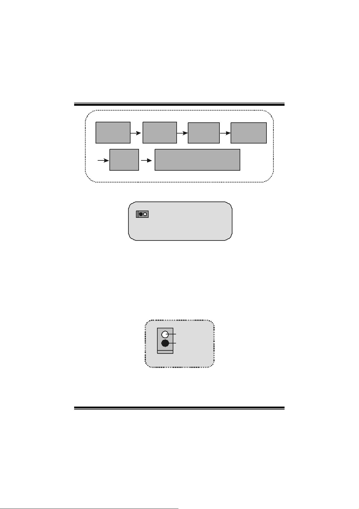
1. Please insert the bootable CD/Floppy Disk
into the boot devices.
2. Press "F 9" after powering on the system.
3. Use the Arrow key to select the boot
devices.
4. Press "Ent er" to start the boot -up process.
is NICE TOUCH
TM
39
Page 42

M
M
M
o
b
r
e
h
t
o
d
r
a
o
D
r
c
s
e
i
r
c
s
e
D
d
r
a
o
b
r
e
h
t
n
o
i
t
p
n
o
i
t
p
i
n
o
i
t
p
i
r
c
s
e
D
d
r
a
o
b
r
e
h
t
o
BIOS STAR -[ FLASHER™ ]
Regularly, when users want t o updat e BIOS, there are two steps to be followed. F irst,
mov e to D OS env ironment. Second, use and maybe download the flash ut ility to update
the BIOS. Unfortunately, there is no DOS support under WindowsR XP. Moreov er, it
tak es t ime t o prepare t he right f lash utility and m ak e a Boot able F loppy Disk if ne ces s ary.
BIOSTAR's [F LASHER ™] technology int egrates flas h utility funct ion onto BI OS firm ware.
The adv ant age is users do not need neither to enter DOS nor to prepare the utility. Jus t
simply enter CMOS and do it.
Flasher Step by S tep
1. Download the latest BI OS file fr om the B IOSTAR website to a floppy disk.
2. Insert the disk tha t contain s the newest BIOS file i nto the floppy drive.
3. Power ON the comput er.
4. Press [DEL] to enter CMOS set up.
5. Select " Upgrade BIOS " item then press Ent er, refer to F igure 1.
40
Page 43

M
M
M
6. Press " Arrow Up/Down " k ey t o choose BIOS f ile, refer to Figure 2
o
o
h
t
h
t
b
r
e
b
r
e
Figure 1
D
d
r
a
o
D
d
r
a
o
i
r
c
s
e
r
c
s
e
n
o
i
t
p
n
o
i
t
p
i
n
o
i
t
p
i
r
c
s
e
D
d
r
a
o
b
r
e
h
t
o
Figure 2
7. Press [Ent er] to load the BIOS from the floppy disk, refer to Figure 3.
41
Page 44

M
M
M
8. At the prom pt "Are y ou sure to flash (Y/N) ", press [Y] t o f lash BIOS or [N] to canc el
the f lashing process , ref er t o Figure 4.
o
o
h
t
h
t
b
r
e
b
r
e
Figure 3
D
d
r
a
o
D
d
r
a
o
i
r
c
s
e
r
c
s
e
n
o
i
t
p
n
o
i
t
p
i
n
o
i
t
p
i
r
c
s
e
D
d
r
a
o
b
r
e
h
t
o
Figure 4
8. After pressing [Y], the f lash starts to process, refer to F igure 5.
42
Page 45

M
M
M
10. A message " Flash done, Restart System (Y/N) " will appear if the system was
suc c essfully updated t he BIOS, ref er to Figure 6.
b
r
e
h
t
o
b
r
e
h
t
o
D
d
r
a
o
D
d
r
a
o
i
r
c
s
e
r
c
s
e
n
o
i
t
p
n
o
i
t
p
i
n
o
i
t
p
i
r
c
s
e
D
d
r
a
o
b
r
e
h
t
o
Figure 6
11. Pres s [Enter], then the f lashing is done!
43
Page 46

M
M
M
o
b
r
e
h
t
o
d
r
a
o
D
r
c
s
e
i
r
c
s
e
D
d
r
a
o
b
r
e
h
t
n
o
i
t
p
n
o
i
t
p
i
n
o
i
t
p
i
r
c
s
e
D
d
r
a
o
b
r
e
h
t
o
Watchdog Technology
It is im portant t o know t hat when overclock ing, the syst em c an b e a t a v u lnerable s tate.
Theref ore, the BIOSTAR Watchdog Tec hnology was designed t o protect y our PC under
dangerous over-cloc k situations. Any over-clock ing that reaches t he threshold settings,
the W atchdog Technology will disable y our system from rebooting in the BIOS setting.
Under this circumstance, please power off your PC. After that, press <Insert> and
power on y our syst em simult aneously t o rest art your system. This user-f riendly des ign
can sav e y ou from s quandering y our time on opening t he case just to c lear the CMOS.
In t he end, thank s t o the Wat c hdog Technology, everything is bac k at a saf e and sound!
44
Page 47

Trouble Shoo ting
p
y
plugg
g up
p
pp
prog
yp
PROBABLE SOLUTION
No power to the system at all Power light don’t
illuminate, fan inside power supply does not turn
on. Indicator light on keyboard does not turn on
PROBABLE SOLUTION
System inoperative. Keyboard lights are on, power
indicator lights are lit, hard drive is spinning.
PROBABLE SOLUTION
System does not boot from hard disk drive, can be
booted from CD-ROM drive.
PROBABLE SOLUTION
System onl y boots from CD-ROM. Hard dis k c an
be read and applications c an be used but booting
from hard dis k is impossi ble.
* Make sure power cable is securely plugged in
* Repla ce ca b le
* Contact techni cal support
* Using even pressure on both ends of the
DIMM,
ress down firmly until the module
snaps into p lace.
* Check cable running from disk to disk controller
board. Make sure both ends are securel
ed in; check the drive type in the
standard CMOS setup.
* Backin
im
breaki ng down at any time.
* Back up data and applic ations fil es. Reformat
the hard drive. Re-install a
using backup disks.
the hard drive is extremely
ortant. All hard disks are capable of
lications and data
PROBABLE SOLUTION
Screen message says “Invalid Configuration” or
“CMOS Fail ure.”
* Review system’s equipment . Make sure
correct info r mat ion is i n setup.
PROBABLE SOLUTION
Cannot boot system after installing second hard
drive.
* Set master/slave jumpers correctly.
* Run SETUP
t
es. Call drive manufacturers for
compatibility with other drives.
ram and select correct drive
45
Page 48

Solución de Problemas
p
g
q
g
p
p
g
p
j
p
p
CAUSA PROBABLE SOLUCIÓN
No hay corriente en el s istema. La luz de corriente
no ilumina, ventilador dentro de la fuente de
alimentación apagada. Indicador de luz del teclado
apagado.
CAUSA PROB ABL E SOL UCIÓN
Sistema inoperativo. Luz del teclado encendido,
luz de indicador de corriente iluminado, disco
rígido está girando.
Sis tema no arranca desde el disco rígido, puede
ser arrancado desde el CD-ROM drive.
Sistema solamente arranca desde el CD-ROM.
Disco rígido puede leer y aplicaciones pueden ser
usados pero el arranque desde el disco rígido es
imposible.
Mensaje de pantalla ”Invalid Configuration” o
“CMOS Fail ure.”
No puede arrancar después de instalar el segundo
disco rígido.
CAUSA PROB ABL E SOL UCIÓN
CAUSA PROBABLE SOLUCIÓN
CAUSA PROBABLE SOLUCIÓN
CAUSA PROBABLE SOLUCIÓN
* Asegúrese que el cable de transmisión esté
seguramente enchufado.
* Reemplac e el c a bl e.
* Contacte ayuda técni ca.
* Presione los dos extremos del DIMM, presione
ara abajo firmemente hasta que el módulo
encaje en el lugar.
* Controle el cable de ejecución desde el disco
hasta el dis co del controlador. Ase
ue ambos lados estén enchufados con
uridad; controle el tipo de disco en la
se
configura ción estánd a r CM OS.
* Co
iando el disco rígido es extremadamente
im
ortante. Todos los discos rígidos son
capac es de dañarse en cualquier momento.
* Copie datos y documentos de aplicación.
Vuelva a formatear el disc o rí
instalar las a
disco de copiado.
* Revis e el equipo del sistema. Asegúrese de
que la información configurada sea correcta.
* Fije cor rect amente el p uen te mas te r/ esclavo.
ec ute el programa SETUP y seleccione el
* E
ti
o de disco correcto. Llame a una
manufacturaci ón del disco
con otros discos.
licaciones y datos usando el
úrese de
ido. Vuelva a
ara compatibilidad
46
Page 49

Problemlösung
m
e
g
p
p
.
g
g
g
p
A
g
g
g
,
p
MÖG LICHE URSACHE LÖSUNG
Das Sys tem hat keine Spannungsversorgung. Die
Stromanzeige leuchtet nicht, der Lüfter im Inneren
der Stromversorgung wird nicht eingeschaltet.
Tastaturleuchten sind nicht an.
MÖG LICHE URSACHE LÖSUNG
Das System funktioniert nicht. Die
Tastaturleuchten sind an, die Stromanzeige
leuchtet, die Festplatte dreht sich.
Das System wird von der Festplatte nicht
hochgefahren, vom CD-ROM-Treiber aber ja.
Das System wird nur von der CD-ROM
hochgefahren. Die Festplatte wird gelesen und die
Anwen dungen sind funk tionsfähi
möglich, das System von der Festplatte zu starten.
Auf dem Bildschirm erscheint die Meldung
“Ungültige Konfigurati on” oder “CMOS Fehler.”
Das System kann nach der Installation einer
zweiten Festplatte nicht hoc hgefahren werden.
MÖG LICHE URSACHE LÖSUNG
MÖG LICHE URSACHE LÖSUNG
, aber es ist nicht
MÖG LICHE URSACHE LÖSUNG
MÖG LICHE URSACHE LÖSUNG
* Versichern Sie sich, da ss das S tromkabel richtig
angebracht ist
* Ersetzen Sie das S tromkabel
* Wenden Si e sich an Ih r e Kundendi enststel le
* Drücken Sie das DIMM-Modul bei gleiche
Druck an beide Seiten, bi s es einrastet.
* Überprüfen Sie das K abel zwischen Festplatte
und Festplatten-Controller. Versichern Si
sich, dass beide Enden richti
sind; über
standardmäßigen CMOS-Einrichtung.
* Ein Bac kup der Festplatte ist sehr wi chti g. Alle
Fest
* Machen Sie eine Sicherun
Daten und Anwendun
Sie die Fest
nwendungen und Daten mit Hilfe von
Backup-Disks.
* Überprü fen Si e die Systemkomponenten und
versi c hern Sie s ich, das di ese ric h ti
eingerichtet sind.
* Setzen Sie die Master/Slave-Jumper richtig ein.
* Führen Sie das SETUP-Pro
wählen Sie die richti
Wenden Sie sich an den Laufwerkhersteller
um die Kom
zu überprüfen.
rüfen Sie den Laufwerktyp in der
la tte n k ö nne n irgendwa nn besc h äd igt we rden
latte und reinstallieren Sie die
ati bilität mit anderen Laufwerken
angebracht
skopie von allen
sdateien. Formatieren
ramm aus und
en Laufwerktypen.
47
Page 50

06/24/2003
48
Page 51

M7NCG BIOS Setup
BIOS Setup........................................................................................1
1 Main Menu..................................................................................................... 3
2 Standard CMOS Features ..............................................................................6
3 Advanced BIOS Features...............................................................................9
4 Advanced Chipset Features..........................................................................12
5 Integrated Peripherals ..................................................................................16
6 Power Management Setup ...........................................................................21
7 PnP/PCI Configurations............................................................................... 24
8 PC Health Status ..........................................................................................26
i
Page 52

M7NCG BIOS Setup
BIOS Setup
Introduction
T his manual discussed Award™ Setup progra m bu ilt into the ROM BIOS. The Setup
program allows users to modify the basic system configuration. This special information is
th en stored in battery -b acked RAM so that it retains the Setup infor mation when t he power
is turned off.
T he Award BIO S™ installe d in your comp ute r sy stem’s RO M (Read Only Memor y) is a
custom version of an industry standard BIOS. This means that it supports AMD
processor input/output system. The BIOS provides critical low-level support for standard
devices such as disk drives and serial and parallel ports.
Addin g important has customized the Award BIOS™, but nonstandard, features such as
virus and password protection as well as special support for detailed fine-tuning of the
chipset controlling the entire system.
The rest of this manual is intended to guide you through the process of configuring your
system using Setup.
Plug a nd Play Support
These AWARD BIOS supports the Plug and Play Version 1.0A specification. ESCD
(Extended System Configurat ion Data) write is supported.
EPA Green PC Support
This AWARD BIOS supports Version 1.03 of the EPA Green PC specification.
APM Support
These AWARD BIOS supports Version 1.1&1.2 of the Advanced Power Management
(APM) specification. Power management features are implemented via the System
Management Interrupt (SMI). Sleep and Suspend power management modes are supported.
Power to the hard disk drives and video monitors can be managed by this AWARD BIOS.
K7
1
Page 53

M7NCG BIOS Setup
PCI Bus Suppo rt
This AW ARD BIOS also supports Version 2.1 of the Intel PCI (Peripheral Component
Interconnect) local bus specification.
DRAM Support
DDR SDRAM (Double Data Rate Synchronous DRAM) are supported.
Supporte d CPUs
This AWARD BIOS supports the AMD
Us ing Set up
In general, you use the arrow keys to highlight items, press <Enter> to select, use the
<PgUp> and <PgDn> keys to change entries, press <F1> for help and press <Esc> to quit.
The following table provides more detail about how to navigate in the Setup program by
using the keyboard.
Keystroke Function
Up arrow Move to p revio us item
Down arrow Move to next item
Left arro w Move to the item o n the left (menu bar)
Right arrow Move to t he item on the right (me nu bar)
Move Enter Move to the item you desired
PgUp key Increase the numeric value or make changes
PgDn key Decrease the numeric value or make changes
+ Key Increase the numeric value or make changes
- Key Decrease the numeric value or make changes
Esc key Main Menu – Quit and not save changes into CMOS
F1 k ey General help o n S et up navigation ke ys
F5 key Load previous values from CMOS
F7 key Load the optimized defaults
F10 key Save all the CMOS changes and exit
®
K7 CPU.
Status Page Setup Menu and Option Page Setup Menu – Exit
Current page and return to Main Menu
2
Page 54

M7NCG BIOS Setup
1 Main Menu
Once you enter Award BIOS™ CMOS Setup Utility, the Main Menu will appear on the
screen. The Main Menu allows you to select from several setup functions. Use the arrow
keys to select among the items and press <Enter> to accept and enter the sub-menu.
!! WARNING !!
The information about BIOS defaults on manual (Fi gu re
1,2,3,4,5,6,7,8,9) is just for reference, please refer to the BIOS
installed on board, for update information.
Figure 1. Main Menu
Standard CM OS Features
This submenu contains industry standard configurable options.
Advanced BIOS Features
This submenu allows you to configure enhanced features of the BIOS.
Advanced Chipset Features
This submenu allows you to configure special chipset features.
3
Page 55

M7NCG BIOS Setup
Integrated Peripherals
This submenu allows you to configure certa in IDE hard drive options and Programmed
Input/ Output features.
Power Management Setup
This submenu allows you to configure the power management features.
PnP/PCI Configurations
This submenu allows you to configure certain “Plug and P lay” and PCI options.
PC Health Status
This submenu allows you to monitor the hardware of your system.
Lo ad Opti mi ze d Defa ul ts
This selection allows you to reload the BIOS when the system is having problems
particu larly w ith the boot sequence. These configurations are factory settings optimized
for this system. A confirmation message will be displayed before defaults are set.
Set Supervisor Password
Setting the supervisor password will prohibit everyone except the supervisor from making
changes using the CMOS Setup Utility. You will be prompted with to enter a password.
4
Page 56

M7NCG BIOS Setup
Set User Password
If the Supervisor Password is not set, then the User Password will function in the same way
as the Supervisor Password. If the Supervis or Pa sswor d is set and the User P as swo rd is
set, the “User” will only be able to view configurations but will not be able to change them.
Save & Exit Se tup
Exit Without Saving
Upgrade BIOS
Save all configuration changes to CMOS(memory) and exit setup. Confirmat ion message
will be displayed before proceeding.
Abandon all changes made during the current session and exit setup. confirmation
message will be displayed before proceeding.
This submenu allows you to upgrade bios.
5
Page 57

M7NCG BIOS Setup
2 Standard CMOS Features
The items in Standard CMOS Setup Menu are divided into 10 categor ies. Each category
includes no, one or more than one setup items. Use the arrow keys to highlight the item and
then use the<PgUp> or <PgDn> keys to select the value you want in each item.
Figure 2. Standard CMOS Setup
6
Page 58

M7NCG BIOS Setup
Main Menu Selections
This table shows the selections that you can make on the Main Menu.
Item Options Description
Date mm : dd : yy Set the system date. Note
Time hh : mm : ss Set the system internal
IDE Primary Master Options are in its sub
menu.
IDE Primary Slave Options are in its sub
menu.
IDE Secondary Master Options are in its sub
menu.
IDE Secondary Slave Options are in its sub
menu.
Drive A
Drive B
Video EGA/VG A
360K, 5.25 in
1.2M, 5.25 in
720K, 3.5 in
1.44M, 3.5 in
2.88M, 3.5 in
None
CGA 40
CGA 80
MONO
that the ‘Day’ automatically
changes when you set the
date.
clock.
Press <Enter> to enter the
sub menu of detailed
options
Press <Enter> to enter the
sub menu of detailed
options.
Press <Enter> to enter the
sub menu of detailed
options.
Press <Enter> to enter the
sub menu of detailed
options.
Select the type of flop p y
disk drive installed in your
system.
Select the default video
device.
7
Page 59

M7NCG BIOS Setup
Item Options Description
Halt On All Errors
No Errors
All, but Keyboard
All, but Diskette
All, but Disk/ Key
Base Memory N/A Displays the amount of
Extended Memory N/A Displays the amount of
Total Memory N/A Displays the total me mory
Select the situation in which
you wa nt the BIOS to stop
the POST process and
notify you.
conventional memory
detected during boot up.
extended memory detected
during boot up.
available in the system.
8
Page 60

M7NCG BIOS Setup
3 Advanced BIOS Features
Figure 3. Advance d BIOS Se tup
Boot Seq & Floppy Setup
First/ Second/ Third/ Boot Other Device
These BIOS attempt to load the operating system from the device in the sequence
selected in these items.
The Choices: Floppy, LS120, HDD-0, SCSI, CDROM, HDD-1, HDD-2, HDD-3,
ZIP100, LAN, HPT370, Disabled, Enabled.
Swap Floppy Drive
For systems with two floppy drives, this option allows you to swap logical drive
assignments.
The Choices: Disabled (default), Enabled.
Boot Up Floppy Seek
Enablin g th is opt ion will test the floppy drives to determine if they have 40 or 80
tracks. Disabling this option reduces the time it takes to boot-up.
The Choices: Disabled, Ena bled (default).
9
Page 61

M7NCG BIOS Setup
Cache Setup
CPU Internal Cache
Depending on the CP U/chipset in use, you may be able to increase memory
access time with this option.
The Choices:
Enabled (default) Enable cache.
Disab led Disab le cache.
External C ac he
This option you to enable or disable “Level 2” secondary cache on the CPU,
which may improve performance.
The Choices:
Enabled (default) Enable cache.
Disab led Disable cache.
Virus Warning
T his option allows you to choo se the Virus Warnin g featur e th at is used to pr ote ct the IDE
Hard Disk boot sector. If this function is enabled and an attempt is made to write to the
boot sector, BIOS will d isp lay a warning message on the screen and sound an alarm beep.
Disabled (default) Virus protection is disabled.
Enabled Virus protection is activated.
Quick Power On Self Test
Enablin g this option will cause an abridged version of the Power On Self-Test (P OST) to
execute after you power up the computer.
Enabled (default) Enable quick POST.
Disabled Normal POST.
Boot Up NumLock Status
Selects the NumLock. State after power on.
On (default) Numpad is number keys.
Off Numpad is arrow keys.
Gate A20 Option
Select if chipset or keyboard controller should control Gate A20.
Normal A pin in the keyboard controller
controls Gate A20.
Fast (default) Lets chipset control Gate A20.
Typematic Rate Se tting
When a key is held down, the keystroke will repeat at a rate determined by the keyboard
controller. When enabled, the typematic rate and typematic delay can be configured.
The Choices: Disabled (default), Enabled.
10
Page 62

M7NCG BIOS Setup
Typematic Rate (Chars /Sec)
Sets the rate at which a keystroke is repeated when you hold the key down.
The Choices: 6 (default), 8,10,12,15,20,24,30.
Typematic Delay (Msec)
Sets the delay time after the key is held down before it begins to repeat the keystroke.
The Choices: 250 (default), 500,750,1000.
Security Optio n
This option will enable only individuals w ith passwords to br ing the system online and/or
to use the CMOS Setup Utility.
System A password is required for the system to boot and is
Setup (default) A password is required to access the Setup Utility
This will only app ly if passwords are set from the Setup main menu.
APIC Mode
By selecting Enabled enables ACPI device mode reporting from the BIOS to the operating
system.
The Choices: Enabled (default), Disabled.
MPS Vers ion Control For OS
The BIOS supports version 1.1 and 1.4 of the Intel multiprocessor specif icat ion.
Select version supported by the operation system running on this computer.
The Choices: 1.4 (default), 1.1.
OS Select For DRAM > 64MB
A choice other than Non-OS2 is only used for OS2 systems with memory exceeding 64MB.
The Choices: Non-OS2 (default), OS2.
Video BIOS Shadow
Determines whether video BIOS will be copied to RAM for faster execution.
The Choices:
Enabled (default) Optional ROM is enabled.
Disabled Optional ROM is disabled.
Summary Screen Show
This item allows you to enable/ disab le display the Summary Screen Show.
The Choices: Disabled (default), Enabled.
also required to access the Setup Utility.
only.
11
Page 63

M7NCG BIOS Setup
4 Advanced Chipset Features
This submenu allows you to configure the specific features of the chipset installed on your
system. This chipset manage bus speeds and access to system memory resources, such as
DRAM. It also coordinates communications with the P CI bus. The default settings that came
with your system have been optimized and therefore should not be changed unless you are
suspic ious that the settings have been changed incorrectly.
Fig ure 4. Adva nced Chipset Setu p
System Perfo rmance
Optimal (Default)
T his it em allows you to use the mos t s tab le settings.
Ag gres sive
This item allows you to use the overclocked settings for higher performance but
with higher risk of inestability.
Expert
T his it em allows fu ll c ust om ization of pe rf orm ance
FSB Frequenc y
This item allows you to select the FSB Frequency.
The Choices: 100MHz (Default)
12
Page 64

M7NCG BIOS Setup
CPU Interface
Optimal (Default)
T his it em allows you to use the mos t s tab le CPU/ FS B parameters .
Ag gres sive
This item allows you to use overclocked CPU/ FSB parameters.
Memory Frequenc y
Select “Auto” for best performance.
Memo ry Ti mi ngs
T(RAS) (Row-active Delay)
This item allows you to set System Performance to “Optimal” to use the delay
recommended by the DIMM’s manufacturer.
T(RCD) (RAS-to-CAS Delay)
This item allows you to set System Performance to “Optimal” to use the delay
recommended by the DIMM’s manufacturer.
T (RP) (Ro w-precharge Delay)
This item allows you to set System Performance to “Optimal” to use the delay
recommended by the DIMM’s manufacturer.
CAS Latency
This item allows you to set System Performance to “Optimal” to use the delay
recommended by the DIMM’s manufacturer.
FSB Spread Spectrum
This item allows you to select the FSB Spread Spectrum.
The Choices: By SPD (Default), 50%, 60%, 66%, 75%, 80%, 83%, 100%, 120%,
125%, 133%, 150%, 166%, 200%, Auto.
Optimal (Default)
T his it em allows you to use the mos t s tab le settings.
Expert
This item allows you to enter timings manually.
The Choices: 7 (Default), 1, 2, 3, 4, 5, 6, 8, 9, 10, 11, 12, 13, 14, 15.
The Choices: 1 (Default), 2, 3, 4, 5, 6, 7.
The Choices: 1 (Default), 2, 3, 4, 5, 6, 7.
The Choices: 2.5 (Default), 2.0, 3.0.
The Choices: 0.50 (Default).
13
Page 65

M7NCG BIOS Setup
AGP Spread Spectrum
This item allows you to select the AGP Spread Spectrum.
The Choices: 0.50 (Default).
Frame Buffer Size
This item allows you to select the Frame Buffer Size.
AGP Aperture Size (MB)
Select the size of the Accelerated Graphics Port (AGP) aperture. The apertures is a portion
of the P CI memory address range dedicated for graphics memory address space. Host
cycles that hit the aperture range are forwarded to the AGP without any translation.
AGP Frequency
This item allows you to select the AGP Frequency.
AGP 8X Support
This item allows you to enable or disable AGP 8X Support.
AGP Fast Write Capability
T his item allows yo u Enab led or Disabled AGP Fast Wr ite Capability .
CPU Thermal Throttling
T his item allows yo u to select the CP U Th ermal Thr ot tlin g.
System BIOS Cacheable
Selecting Enabled allows you cachin g of the system BIOS ROM at F0000h~FFFFFh,
resultin g a better system performance. However, if any program writes to this memory area,
a system error may result.
The Choices: 32M (Default), 8M, 16M, 64M, 128M, Disabled.
The Choices: 64 (default), 4, 8, 16, 32, 128, 256.
The Choices: Auto (Default), 50MHz , 66MHz, 67M Hz, 68MHz , 69MHz,
70MHz, 71MHz, 72MHz, 73MHz, 74MHz, 75MHz, 76MHz, 77MHz, 78MHz,
79MHz, 80MHz, 81MHz, 82MHz, 83MHz, 84MHz, 85MHz, 86MHz, 87MHz,
90MHz, 93MHz, 95MHz, 97MHz, 100MHz.
The Choices: Enabled (Default), Disabled.
The Choices: Enabled (Default), Disabled.
The Choices: 50% (Default), Disabled, 87.5%, 75%, 62.5%, 37.5%, 25%,
12.5%.
The Choices: Enabled , Disabled (default).
14
Page 66

M7NCG BIOS Setup
Video RAM Cacheable
Enablin g this option allows caching of the video R AM, resulting a better system
performance. However, if any program writes to this memory area, a system error may
re su lt.
The Choices: Disabled (default), Enabled.
TV Mode Support
This option allows you to decide whether or not to connect the computer with a television.
The Choices: Disabled (default), Enabled.
15
Page 67

M7NCG BIOS Setup
5 Integrated Peripherals
Figure 5. Integrated Peripherals
IDE Function Setup
The chipset contains a PCI IDE interface with support for two IDE channels.
Select “Enabled” to activate the first and / or second IDE interface. If you install a primary
and / or secondary add-in IDE interface, select “Disab led” to deactivate an interface. If you
hi gh light the litera l “P r ess Enter” next to t he “Onchip ID E Control” lab e l and then press the
enter key, it will take you a submenu with the following options:
OnChip IDE Channel 0/1
The motherboard chipset contains a PCI IDE interface with support for
two IDE channels. Select “Enabled” to activate the first and/or second IDE
interface. Select “Disabled” to deactivate an interface if you are going to install a
primary and/or secondary add-in IDE interface.
The Choices: Enabled (default), Disabled.
IDE Prima ry / Secondary Master / Slave PIO
The IDE P IO (Programmed Input / Output) fields let you set a PIO mode (0-4)
for each of the IDE devices that the onboard IDE interface supports. Modes 0
through 4 provides successively increased performance. In Auto mode, the
system automatically determines the best mode for each device.
The Choices: Auto (default), Mode0, Mode1, Mode2, Mode3, Mode4.
16
Page 68

M7NCG BIOS Setup
IDE Prima ry / Secondary Master / Slave UDMA
Ultra DMA/100 functionality can be implemented if it is supported by the IDE
hard drives in your system. As well, your operating environment requires a DMA
driver (Windows 95 OSR2 or a third party IDE bus master driver). If your hard
drive and your system software both support Ultra DMA/100, select Auto to
enable BIOS support.
The Choices: Auto (default), Disabled.
IDE Prefetch Mode
The “onboard” IDE drive interfaces supports IDE prefetching for faster drive
access. If the interface does not support prefetching. If you install a primary
and/or secondary add-in IDE interface, set this option to “Disabled”.
The Choices: Enabled (default), Disabled.
IDE HDD Block Mode
Blo ck mode is a ls o called b lock t ran sfer, mu ltiple c omma nds , or m ultip le secto r
read / write. If your IDE hard drive supports block mode (most new drives do),
select Enabled for automatic detect ion of the optimal number of block mode
(most new drives do), select Enabled for automatic detection of the optima l
number of block read / write per sector where the drive can support.
The Choices: Enabled (default), Disabled.
Onboa rd Device
AC97 Audio
This item allows you to decide to enable/ disab le to support AC97 Audio.
The Choices: Auto (default), Disabled.
AC97 Modem
This item allows you to decide to enable/ disab le to support AC97 Modem.
The Choices: Auto (default), Disabled.
MAC LAN (nVIDIA)
T his it em allows you to select MAC LAN.
The Choices: Auto (Default), Disabled.
Ma chi ne M AC (NV) Add ress
This item allows you to enable or disable Machine MAC Address.
The Choices: Disabled (Default), Enabled.
Onchip 1394 Chip
This item allows you to set the Onchip 1394 Chip.
The Choices: Auto (Default), Disabled.
Init Display First
This item allows you to decide to active whether PCI Slot or on-chip VGA first.
The Choices: Onboard/AGP, PCI So lt (default).
17
Page 69

M7NCG BIOS Setup
OnChip USB
T his item allows yo u to set the onchip USB.
The Choices: V1.1+V2.0 (default), Disabled, V1.1.
USB Keyboard Suppo rt
T he de fault value is Disab led .
Enabled Enable USB Keyboard Support.
Disabled (default) Disable USB Keyboard Support.
Onboa rd I/O Chi p Se tup
Power On Function
This item allows you to choose the powen on function.
The Choices: Button only (default), Password, Hot Key, Mouse Left, Mouse
Right, Any Key, Keyboard 98.
KB Po wer o n Posswo rd
Input password and press Enter to set the Keyboard power on password .
HOT Key power ON
Input password and press Enter to set the Keyboard power on password .
The Choices: Ctrl-F1(default) , Ctrl-F2 , Ctrl-F3 , Ctrl-F4 , Ctrl-F5,
Ctrl-F6 , Ctrl-F7 , Ctrl-F8 , Ctrl-F9, Ctrl-F10 , Ctrl-F11 , Ctrl-F12 .
On bo ard FD C Co nt ro ller
Select Enabled if your system has a floppy disk controller (FDC) insta lled on the
system board and you wish to use it. If install and FDC or the system has no
floppy drive, select D isabled in this field.
The Choices: Enabled (default), Disabled.
On bo ard S eria l P ort 1
Select an address and corresponding interrupt for the first and second serial ports.
The Choices: 3F8/IRQ4 (default), Disabled, Auto, 2F8/IRQ3,
3E8/IRQ4, 2E8/IRQ3.
On bo ard S eria l P ort2
Select an address and corresponding interrupt for the first and second serial ports.
The Choices: Disabled (default), 3F8/IRQ4, 2F8/IRQ3, 3E8/IRQ4, 2E8/IRQ3,
Auto.
UART Mode Select
This item allows you to determine which Infra Red (IR) function of onboard I/O
chip.
The Choices: Normal, ASKIR, IrDA (default).
18
Page 70

M7NCG BIOS Setup
RxD, Tx D Active
This item allows you to determine which Infrared (IR) function of onboard I/O
chip.
The Choices: Hi / Lo (default), Hi / Hi, Lo / Hi, Lo / Lo.
IR Transmissio n Delay
T his it em allows you to enable/d isab le IR transmiss io n delay.
The Choices: Enabled (default), Disabled.
UR2 Duplex Mode
Select the value required by the IR device connected to the IR port. Full-duplex
mo de p erm its simultaneous two-d irect ion tran sm iss ion. Half-duplex mode
permits transmission in one direction only at a time.
The Choices: Half (def ault ), Full.
Use IR Pins
Consult your IR peripheral documentation to select the correct setting of the TxD
and RxD signals.
The Choices: IR-Rx2Tx2 (default), RxD2, TxD2.
Onboard Parallel Port
This item allows you to determine access onboard parallel port controller with
which I/O address.
The Choices: 378/IRQ7 (default), 278/IRQ5, 3BC/IRQ7, Disabled.
Parallel Port Mode
The default value is SPP.
SPP (default) Usin g Paralle l port as Standard P rinter P ort.
EP P Us in g Parallel por t a s En hanced P ara lle l
Port.
EC P Us in g Parallel port a s Extended Ca pabilities
Port
EC P+EPP Using Pa ralle l por t a s EC P & EPP mode.
EPP Mode Select
Select EPP port type 1.7 or 1.9.
The Choices: EPP 1.7(default), EPP1.9.
ECP Mode Use DMA
Select a DMA Channel for the port.
The Choices: 3 (default), 1.
Game Port Address
Game Port I/O Address.
The Choices: 201 (default), 209, Disabled.
19
Page 71

M7NCG BIOS Setup
Midi Port Address
Midi Port Base I/O Address.
The Choices: 330 (default), 300, 290, Disabled.
Midi Port IRQ
This determines the IRQ in which the Midi Port can use.
The Choices: 10 (default), 5.
20
Page 72

M7NCG BIOS Setup
6 Power Management Setup
The Power Management Setup Menu allows you to configure your system to utilize energy
conservation and power up/power down features.
Figure 6. Power Manage ment Setup
ACP I function
This item displays the status of the Advanced Configuration and Power Management
(ACPI).
The Choices: Enabled (default), Disabled.
ACP I Suspend Type
The item allows you to select the suspend type under the ACPI operating system.
The Choices: S1 (POS) (default) Power on Suspend
S3 (STR) Suspend to RAM
S1 & S3 P OS+STR
Power Manage ment
This category allows you to select the type (or degree) of power saving and is directly
related to the following modes:
1.HDD Power Down.
2. Suspend Mode.
There are four options of Power Management, three of which have fixed mode settings
21
Page 73

M7NCG BIOS Setup
Min. Power Saving
Minimum power management.
Su spe nd M ode = 1 hr .
HDD Power Down = 15 min
Max. Power Saving
Maximum power management only available for sl CPU’s.
Su spe nd M ode = 1 min.
HDD P ower Down = 1 min.
User De fined (default)
Allows you to set each mode individually.
When not disabled, each of the ranges are from 1 min. to 1 hr. except for HDD
Power Down which ranges from 1 min. to 15 min. and disable.
Video Off Method
T his option deter mines the man ner in which th e monitor is goes blank.
V/H SYNC+Blank
This selection will cause the system to turn off the vertical and horizontal
synchronization ports and write blanks to the video buffer.
Blank Screen
This option only writes blanks to the video buffer.
DPMS (default)
In itia l d isplay powe r managem ent signa lin g.
HDD Power Down
When enabled, the hard disk drive will power down and after a set time of system inactiv ity.
Al l other device s r emain act ive .
The Choices: Disabled (default), 1 Min, 2 Min, 3 Min, 4 Min, 5 Min, 6 Min, 7 Min,8 Min,
9 Min, 10 Min, 11 Min, 12 Min, 13 Min, 14 Min, 15Min.
HDD Down In Suspend
This item allows you to enable or disable HDD Down In Suspend.
The Choices: Disabled (Default), Enabled.
Soft-Off by PW R-BTTN
Pressing the power button for more than 4 seconds forces the system to enter the
22
Page 74

M7NCG BIOS Setup
Soft-Off state when the system has “hung.”
The Choices: Delay 4 S ec, Instant-Off (default).
WOL (PME# ) From Soft-Off
This item allows you to enable or disable the WOL (PME#) From Soft-Off.
The Choices: Disabled (Default), Enabled.
WOR (RI#) From Soft-Off
This item allows you to enable or disable the WOR (RI#) From Soft-Off.
The Choices: Disabled (Default), Enabled.
USB Resume from S3/ S4
T his item allows yo u to enab le or disable USB Res ume from S3 / S4.
The Choices: Disabled (Default), Enabled.
Power-On by Alarm
This item allows you to enable or disabled power on by alarm.
The Choices: Disabled (Default), Enabled.
23
Page 75

M7NCG BIOS Setup
7 PnP/PCI Configurations
This section describes configur ing the PCI bus system. PCI, or Personal Computer
Interconnect, is a system which allows I/O devices to operate at speeds nearing the speed of
the CPU itself uses when communicating with its own special components. This section
covers some very technical items and it is strongly recommended that only experienced
users should make any changes to the default settings.
Figure 7. PnP/PCI Configurations
Reset Configuration Data
The system BIOS supports the PnP feature which requires the system to record which
resources are assigned and protects resources from conflict. Every peripheral device has a
node, which is called ESCD. This node records which resources are assigned to it. The
system n eed s to record and update ESCD to the me mor y lo cat ions. These locat ions (4 K)
are reserved in the system BIOS. If the Disabled (default) option is chosen, the system‘s
ESCD will update only when the new configuration varies from the last one. If the Enabled
option is chosen, the system is forced to update ESCDs and then is automatically set to the
“D isabled” mod e.
The above settings will be shown on the screen only if “Manual” is chosen for the resources
controlled by function.
Le gacy is the term, which sign ifies that a resource is ass igned to the ISA Bu s and prov ides
24
Page 76

M7NCG BIOS Setup
non-PnP ISA add-on cards. PCI / ISA P nP sign ifies that a resource is assigned to the P CI
Bus or provides for ISA PnP add-on cards and peripherals.
The Choices: Disabled (default), Enabled.
Resource s Co ntrolled B y
By Choosing “Auto(ESCD)” (default), the system BIOS will detect the system resources
and automatically assign the relative IRQ and DMA channel for each peripheral.By
Choosin g “Manual”, the user will need to assign IRQ & DMA for add-on cards. Be sure
that there are no IRQ/DMA and I/O port conflicts.
IRQ Resources
This submenu will allow you to assign each system interrupt a type, depending on the type
of device using the interrupt. When you press the “Press Enter” tag, you will be directed to
a submenu that will allow you to configure the system interrupts. This is only
configurable when “Resources Controlled By” is set to “Manual”.
IRQ-3 assigned to PCI Device
IRQ-4 assigned to PCI Device
IRQ-5 assigned to PCI Device
IRQ-7 assigned to PCI Device
IRQ-9 assigned to PCI Device
IRQ-10 assigned to PCI Device
IRQ-11 assigned to PCI Device
IRQ-12 assigned to PCI Device
IRQ-14 assigned to PCI Device
IRQ-15 assigned to PCI Device
PCI / VG A Palette Snoo p
Choose Disabled or Enabled. Some graphic contro llers which are not VG A compatible
take the output from a VGA controller and map it to their display as a way to provide boot
informat ion and VGA compatibility.
However, the color information coming from the VGA controller is dra wn f ro m the pa lette
table inside the VGA controller to generate the proper colors, and the graph ic controller
needs to know what is in th e palette of the VGA contro ller. To do this, the no n-VGA
graphic controller watches for the Write access to the VGA palette and registers the snoop
data. In P CI ba sed sy stems, wh ere the VGA co ntroller is on the PCI bus and a non-VGA
graphic controller is on an ISA bus, the Write Access to the palette will not show up on the
ISA bus if the PCI VGA controller responds to the Write.
In this case, the P CI VGA contro ller s hou ld not res pond to the Write, it should only sn oop
the data and permit the access to be forwarded to the ISA bus. The non-VGA ISA graphic
controller can then snoop the data on the ISA bus. Unless you have the above situation,
you should disab le th is option.
Disabled (default) Disab les the function.
Enabled Enables the function.
25
Page 77

M7NCG BIOS Setup
8 PC Health Status
Figure 8. PC Health Status
Current CPU Temperature
Show you the current CP U temperature.
Current SYSFAN Speed
This field displays the current SYSFAN speed.
Current CPUFAN Speed
This field displays the current CPUFAN speed.
CPU Vcore/AGP Vcore/AGP Voltage/+3.3V/+12V/-12V/-5V
Detect the system’s voltage status automatically.
Show H/W Monitor in POST
If you computer contain a monitoring system, it will show PC health status during P OST
stage. The item offers several delay time to select you want.
The Choices: Enabled (default), Disabled.
26
Page 78

M7NCG BIOS Setup
Chassis Open Warning
This item allows you to enable or disable Chassis Open Warning beep.
The Choices: Disabled (Default), Enabled.
27
 Loading...