

Biostar M6VLQ Grand Owner's Manual

M
i
6
V
L
Q
G
r
a
n
d
M
M
6
6
V
V
L
L
Q
Q
G
G
r
r
a
a
n
n
d
d
FCC Infor mation and Copyright
This equipment has been tested and found to com ply with the limits of a
Class B digital device, pursuant to Part 15 of the FCC Rules. T hese limits
are designed to provide reasonable protection against harmful
int erference in a residential ins t allation. This equipment g enerat es, uses
and can radiate radio frequency energy and, if not installed and used i n
ac cordan ce wit h the in stru ction s, ma y cau se harm fu l in terf eren ce t o radi o
communications. There is no guarantee th at interference will not occur in
a partic ular installation.
The vendor makes no repr esentations or warranties with respect to the
contents here of and specially disclaims any implied
merchantabi li ty or fitness fo r a ny purpose. F urther the vendor reserves
the right to revise this publication and to make changes to the contents
here of without obligation to notify any party beforehand.
Duplication of this publication, in part or in whole, is not allowed without
first obtaining the vendor’s approval in writing.
The con tent of this user’s manual is subject to be changed without notice
and we will not be responsible for any mistakes found in this user’s
manual. All the brand and product names are trademarks of their
r es p e c t iv e co m pa ni e s.
warran ties of

C
C
C
o
o
t
n
e
t
n
t
n
e
t
n
t
n
e
t
n
o
LAYOUT OF M6V LQ GRAND............................................................... 1
COMPONENT INDEX............................................................................. 2
ENGLISH...................................................................................................3
M6VLQ Pro Features..................................................................................3
Packag e contents.......................................................................................4
How to setup Jumper.................................................................................5
CPU Ins t alla tion......... ........................ ........................................................5
DIMM Modules: DIMM1/ DIMM2 ....................................................................6
Jumpers, Headers, Connectors & Slots.........................................................7
ESPAÑOL ................................................................................................12
Características del M6VLQ Pro..................................................................12
Co nt enido del Paquete........... ........................ ........................ ..................13
Cómo instalar un Puente........................................................................... 14
Instalación de la CPU................................................................................ 14
Módulos DIMM: DIMM1/ D IMM2..................................................................15
Puentes, C abezales, Con ectores y Ranuras................................................16
WATCHDOG TECHNOLOGY.............................................................21
WARPSPEEDER..................................................................................... 22
Introdu ction.............................................................................................22
System Requirement................................................................................22
Installation ..............................................................................................23
Usage.....................................................................................................24
STUDI OFUN!
Introdu ction.............................................................................................32
Hardware Re qui re m e nts.................................. ........................ ..................32
Installation and Usag e..............................................................................32
TM
(OPTIO NAL).............................................................32
TROUBLE SHOOTIN G......................................................................... 33
SOLUCIÓN DE PROBLEMAS.............................................................34
ii
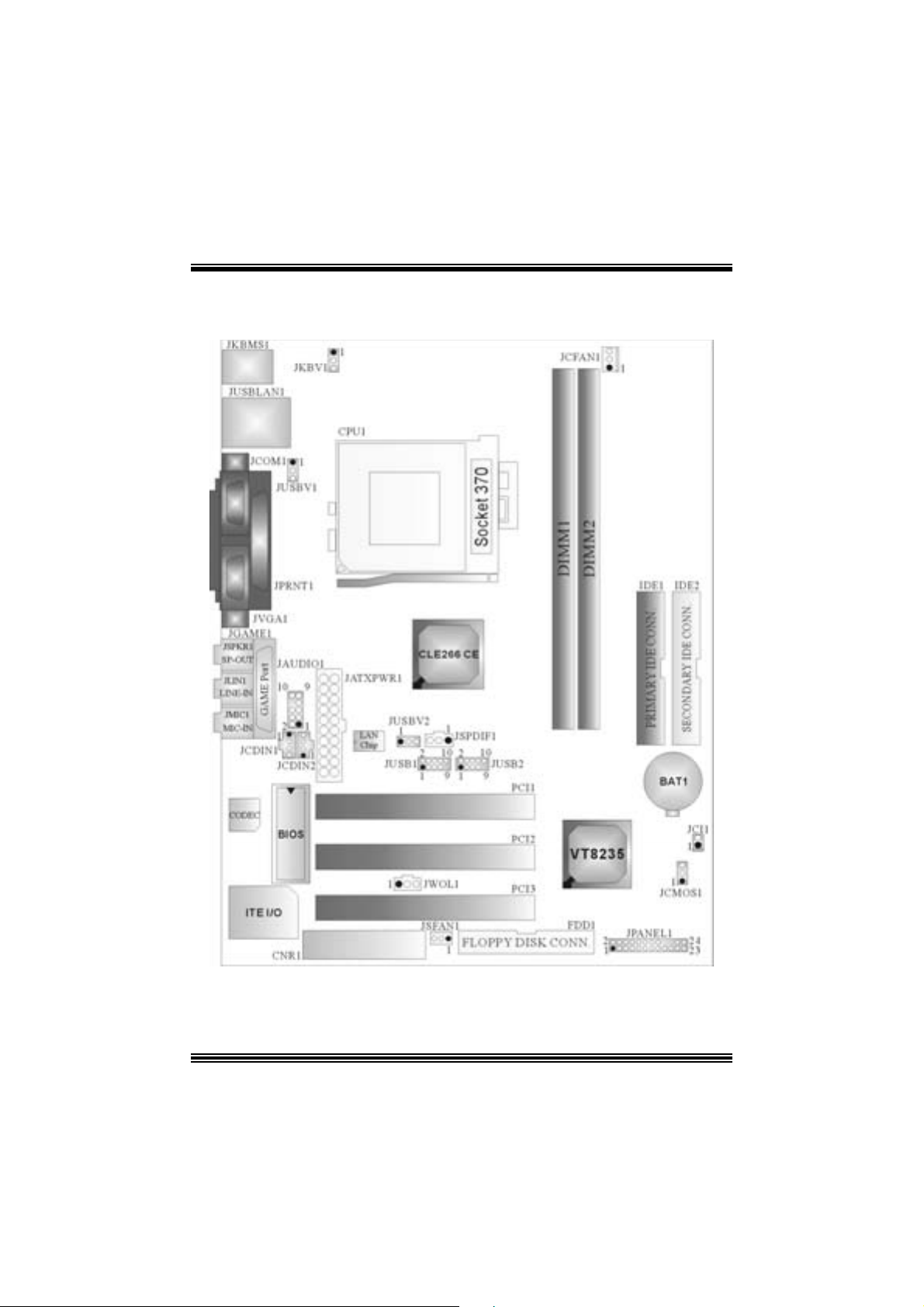
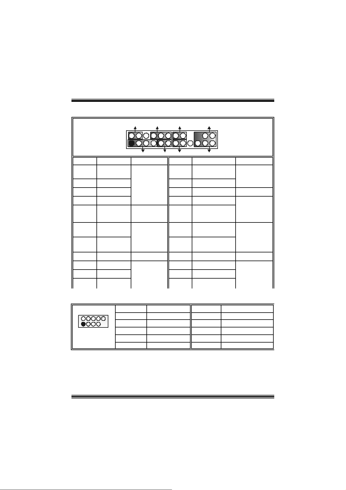
Layout of M6VLQ G rand
※NOTE: ●represent s the f irst pin.
1
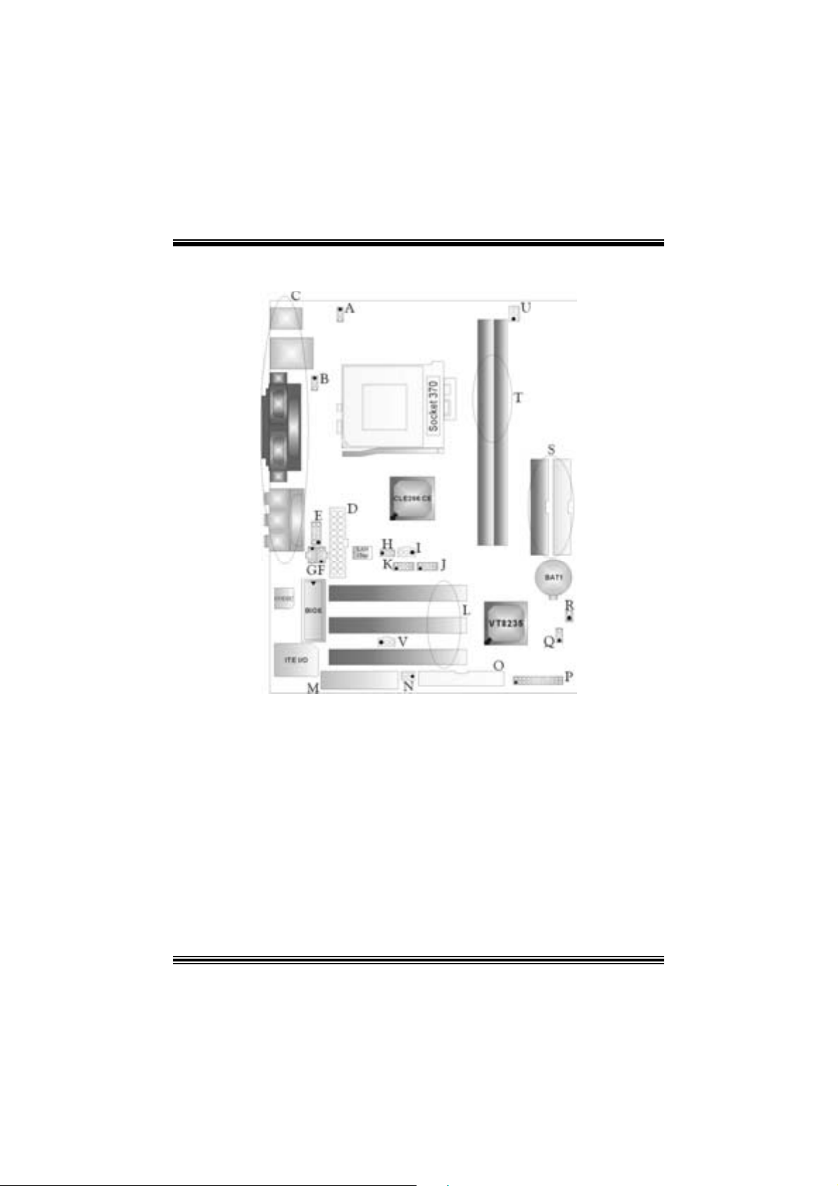
Compone nt Index
A. Power Source Selection for K. Front USB Header (JUSB 1)
Keyboard and mouse (JKBV1) L. PCI BUS Slots (PCI 1-3)
B. Power Source Selection for USB M. Communication Net work Riser Slot
(JUSBV1) (CNR1)
C. Back Panel Connector N. System Fan Header ( JSF AN1)
D. A TX Power Connector (JATX PWR1) O. Floppy Disk Con nector (FDD1)
E. Front Audio Header (JAUDIO 1) P. Front Panel Connector (JPA NEL1)
F. CD Audio-I n Header (J CDIN2) Q. Clear CMOS Func ti on (JCMOS1)
G. CD Audio-In Header (JCDIN1) R. Case Open Connector (JCI1)
H. Power Source Selection for USB S. IDE Connectors (IDE1-2)
(JUSBV2) T. DIMM Modul es (DIMM1-2)
I. Digital Audio Connector (JSPDI F1) U. CPU Fan Head er (JCFAN1)
J. Front USB Header (JUSB2) V. W ake On LAN Header ( JWOL1)
2

English
M6VLQ Pro Features
A. Har dware
CPU
Prov ides Sock et 370.
Supports Celeron™ proc essor PPGA (FC -PGA & FC-PGA2) and the Pentium® III
Micro-Proc es s or (FC-PGA & FC-PGA2) and VIA C 3 Ezra and Ezra-T Samuel 2 f or
high-end work s tations and s ervers.
F ront Side Bus at 66/100/ 133 MH z.
Chipset
N orth Bridge: VIA CLE266 CE.
Sout h Bridge: VIA VT8235.
Main Me m o ry
Support s up t o 2 DDR devices .
Support s 200/ 266 MH z (without ECC) DDR devices.
Maxi mu m me mo ry s i ze o f 2GB.
Lan Chip (optiona l)
Chip: VI A VT6103.
Supports 10 Mb/s and 100 Mb/ s auto-negot iat ion
H alf / Full duplex capability.
Slots
Three 32-bit PCI bus master s lots.
One CNR slot.
On Board IDE
Supports four IDE di s k dri ves.
Supports PIO Mode 4, Bride Mode and U lt ra DMA 33/66/100/ 133 Bus Master
Mode.
Super I/O
Chip: ITE IT 8705.
Prov ides the most commonly used legacy Super I/O f unctionality .
Env iro nm ent C ont rol i niti atives
- H/W Monitor
- Fan Speed Controller
- I TE's "Smart Guardian" f unction
On Bo ard AC’97 Sound Cod ec
Chip: VI A VT1612A.
AC ’97 2. 2 S/ PDIF ex t ens ion com pliant codec.
18-bit stereo full duplex.
3
On Board Periphera ls
a. R ear si d e
1 s erial port.
1 VGA port.
1 p arallel po rt. (SPP/ EPP/EC P mode)
1 a udio port in hori zontal pos itio n.
1 L AN jack.
PS/2 mouse and PS/2 keyboard.
2 USB2.0 ports.
b. F r ont Si de
1 fl oppy port su pport s 2 F DDs w ith 3 60K, 720K, 1. 2M, 1.44M and 2.88Mby tes.
4 USB2.0 ports.
1 S/PDIF Out Connector.
Dimensions
Mic ro ATX Form Fac t or: 19 X 24.4cm (W X L)
B. BIOS & S oftware
BIOS
Award legal Bios .
Support s APM1.2.
Support s AC PI.
S upports USB Func tion.
Software
S uppor ts W atchd ogTM, 9t h T ouc hTM, FLASHER™, St udioF un !
Warpspeeder
Offers the highest performance for Windows 98 SE, Windows 2000, W indows Me,
Windows XP, SC O UNIX etc.
TM
.
TM
(optional),
Package contents
HDD Ca b le X1
FDD Cable X1
User’s Manual X1
USB Cable X1 (optional)
Rear I/ O Panel for ATX Cas e X1 (optional)
Fully Setup Driver CD X1
S/ PD IF Cable X1 (opt ional)
St udioF un! Application CD X1 (optional)
4
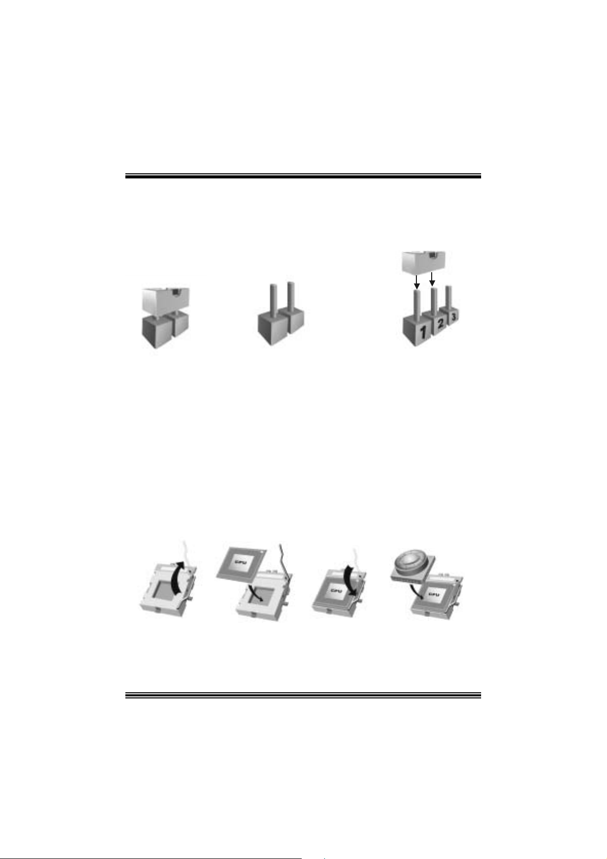
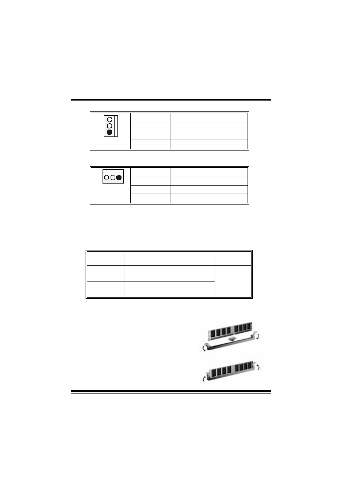
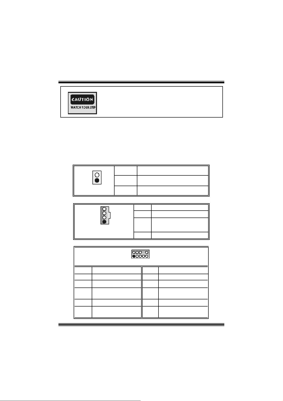
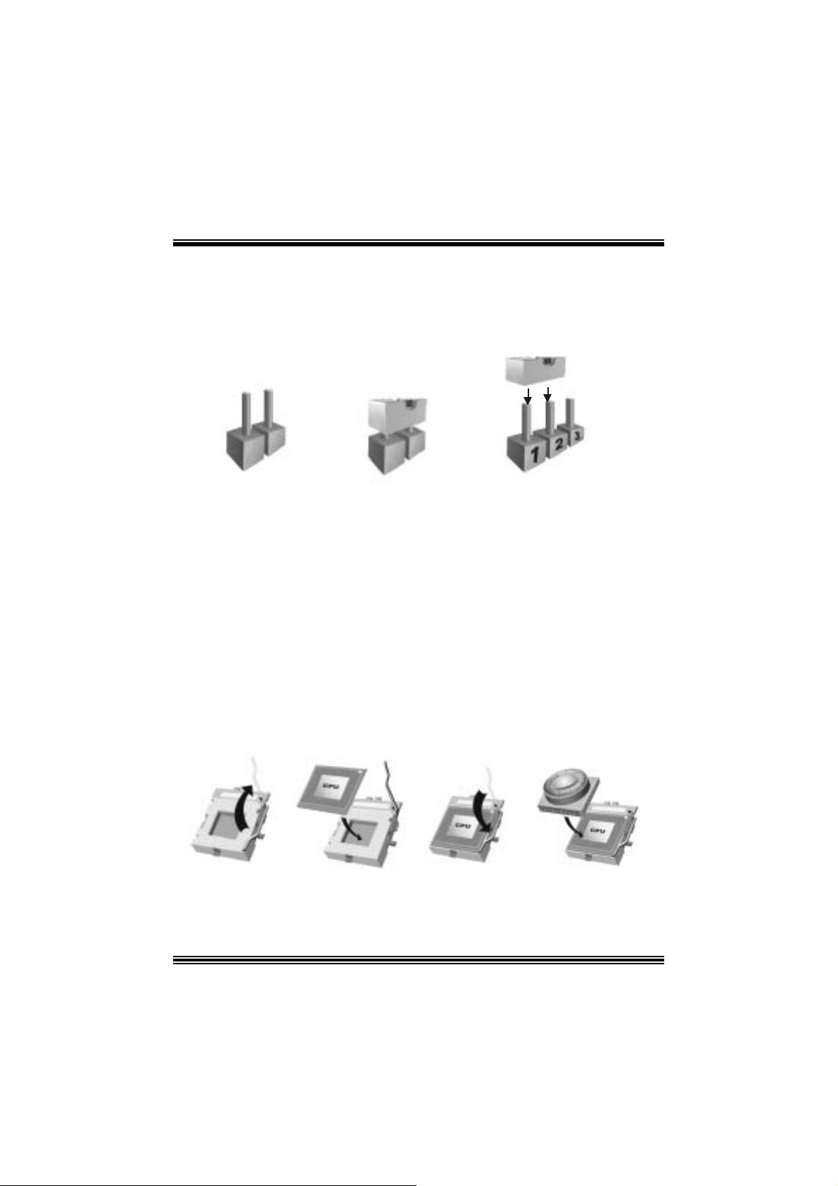
Ho w to setup Jumper
The illustrat ion sho ws how jum pe rs are s e tu p. When the Jum per c ap is placed on pins, the
jumper is “close”. If no jumper cap is placed on the pins, the jumper is ”open”. The
illust rat ion sho ws a 3-pin jumper whos e pin 1and 2 are “close” when jumper c ap is placed
on thes e 2 pins .
Jumper close Jumper open Pi n1-2 close
CPU Installation
Step1: Pull the lever sideway s away from the s ock et and then raise the lever up to a
90 -degree angl e.
Step2: Look for the white dot/c ut edge. The whit e dot/cut edge should point towards the
lev er pivot. The C PU will f it only in the c orrect orient ation.
Step3: Hold the CPU down fir ml y, and then close the lever.
Step4: Put t he C PU f an on t he C PU and buck le it. Connect the CPU fan power c able t o
the JCFAN1. This completes the installation.
Step1 Step2 Step3 Step4
5
CPU Fan Header: JC FAN1
Pin No. A ssi gnm e nt
1
JCFAN1
1
2
3
FAN rpm Rate Sense
Ground
+12V
S ystem Fan Header: JSFAN1
Pin No. A ssi gnm e nt
13
JSFAN1
1
2 +12V
3
FAN rpm Rate Sense
Ground
DIMM Modu le s: DI MM1/ DIMM2
DR AM Access Time: 2.5V Un buff ere d DDR 200/266 MHz Type requ ired.
DRAM Type: 64MB/ 128MB/ 256MB/ 512MB/ 1GB DI MM Module (184 pin)
Total Memory Size wit h Unbuffere d DI MM s
DI MM S ocket
DDR Mod u l e To tal Memory
Location
DIMMB1 64MB/128MB/256MB/512MB/1GB
DIMMB2 64MB/128MB/256MB/512MB/1GB
***On ly for refer en ce***
Installing DDR Module
1. Unlock a DIMM slot by pressing the
retaining clips outward. Align a DIMM on
t he s lot s uc h t hat t he no t c h on th e D IMM
ma t ches t he break o n the sl ot .
2. I nsert the DIMM f irmly and vertically into
the s lot until the ret ain ing c hip s nap back in
place and the Dimm is properly seat ed.
*1
*1
6
Size (MB)
Max is
2GB
Jumpers, Headers, Connectors & Slots
Floppy Disk Connector: FDD1
The mot herboard provides a standard f loppy disk connector that supports 360K,
720K, 1.2M, 1.44M and 2.88M floppy disk types. This connector supports the
prov ided f loppy drive ribbon cables .
Hard Disk Connectors: IDE1/ IDE2
The motherboard has a 32-bit Enhanced PCI IDE Controller that provides PIO
Mode 0~4, Bus Mast er, and Ultra DMA 33/ 66/ 100/ 133 functionality. It has t wo
HDD connec t ors IDE1 (primary) and IDE2 (secondary).
The ID E c onnectors can c onnect a master and a slav e driv e, so y ou can c onnect
up to four hard disk drives . The f irst hard drive s hould alway s be c onnected t o
IDE1.
Peripheral Component Interconnect Slots: PCI 1-3
This m ot herboard is equipped with 3 st andard PCI s lots. PCI stands for Peripheral
Component I nterconnec t, and it is a bus standard for expansion cards. This PCI
slot is des ignated as 32 bits.
Commun ication Netwo r k R ise r Slot: CNR1
The CNR specification is an open I ndust ry St andard Architecture, and it def ines a
ha rdw ar e scalable r iser card interfa ce, which su pports modem only.
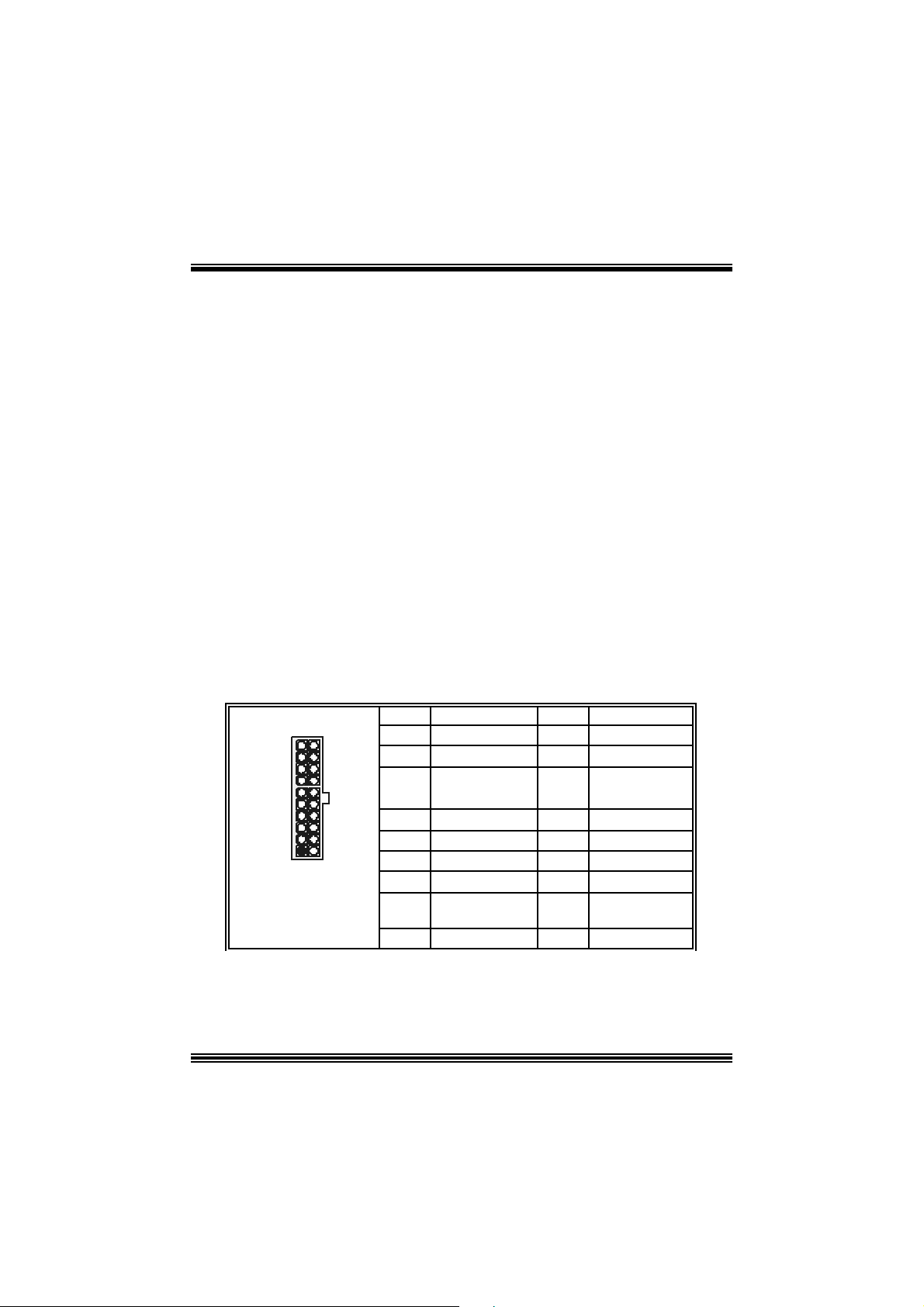
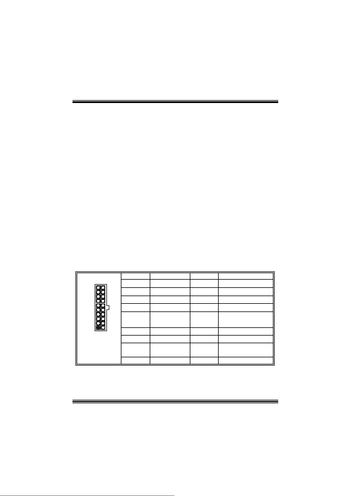
Power Conn ectors: JATXPWR1
10
1
JATXPWR1
20
11
PIN Assignment PIN Assignment
1 +3.3V 11 +3.3V
2 +3.3V 12 -12V
3 Ground 13 Ground
4 +5V 14 PS_ON
5 Ground 15 Ground
6 +5V 16 Ground
7 Ground 17 Ground
8 PW_OK 18 -5V
9 Standby Voltage
+5V
10 +12V 20 +5V
7
19 +5V
0
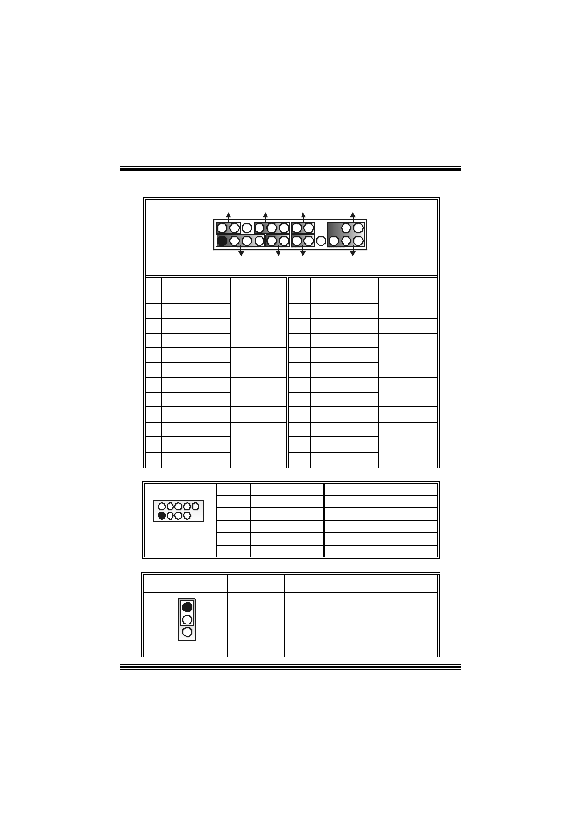
Front Pane l Conne ctor: JPANEL1
SLP
JPANEL1
Pin Assignment Function Pin Assignment Function
1 +5V 2 Sleep Control
3 NA 4 Ground
5 NA 6 NA NA
7 Speaker
9 HDD L E D ( +) 10 Power LED (+)
11 H DD LED (-)
13 Ground 14 Power Button
15 Reset Control
17 NA 18 KEY
19 NA 20 KEY
21 +5V 22 Ground
23 IRTX
2
123
PWR_LED
(+) (-)(+)
SPK
Hard Dr ive
(+) (-)
HLED
RST
Speaker
Connector
8 Power L ED (+)
LED 12 Power LED (-)
Reset
Button
IrDA
Connector
16 Ground
24 IRRX
IRON/ OFF
IR
24
Sleep
Button
POWER
LED
Power-on
Button
IrDA
Connector
Front USB Header: JUSB1/2
2
1
JUSB1/2
Pin Assignment Pin Assignment
1
1
3
9
5
7
9
+5V(fused)
USBP4-
USBP4+
Ground
KEY
2
4
6
8
10
+5V(fused)
USBP5-
USBP5+
Ground
NA
Power Source Selection for Keyboard/ Mo use: JKBV1
JKBV1 Assignment Description
1
3
Pin 1-2 c los e
+5 V
+5V for keybo ard and mouse
8
h
1
3
Pin 2-3 c los e
+5V Standby
Voltage
PS/2 Mous e and PS/2 Key board are
powered with +5V standby v oltage
No te: In or der to suppo rt thi s f un cti on “P ow er-on th e syst em v i a ke ybo a rd
and mouse”, “JKBV1” jumper cap should be placed on pin 2-3.
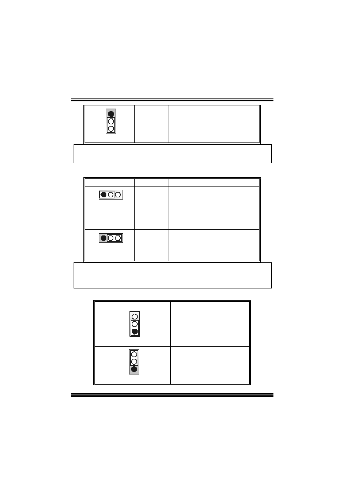
Power Source Selection for USB: JUSBV1/ JUSBV2
JUSBV1/JUSBV2 Assignment Description
1 3
Pin 1-2 c los e
1 3
Pin 2-3 c los e
Note: In order to support this function “Power-on the system via USB
devices”, “JUSBV1/ JUSBV2” jumper cap should be placed on pin 2-3
respectivel y.
+5V JUSBV1: 5V for USB connec tors
located at the JUS BLAN1 connector
port
JUSBV 2: 5V for USB connec tors
lo cated at the JUSB 1/2 connector ports
+5V Standby
Voltage
JUSBV1: JU SBLAN1 port powered wit
JUSBV2: JUSB1/2 ports powered wit h
standby v olt age of 5V
standby v olt age of 5V
Clear CMOS Jumper: JCMOS1
JCMOS1 Assignment
3
1
Pin 1-2 C lose
3
1
Pin 2-3 C lose
9
Norm al Operation (def ault)
Clear CMOS Data
The following procedures are for resetting the
BIOS password. It is important to follow these
instructions closely.
※ Cle ar CMOS Procedures:
1. R emov e AC power line.
2. Set the jumper to “Pin 2-3 C lose”.
3. Wa it for fi ve seconds.
4. Set the jumper to “Pin 1-2 C lose”.
5. Power on t he AC .
6. R eset your des ired password or clear t he C MOS dat a.
Ca se Op e n Connec to r: JCI1
Assignment
Case Open Signal
Ground
1
JCI1
Pin
1
2
CD-ROM Audio-In Heade r: JCDIN1/ JCDIN2
4
1
JCDIN1/2
Pin Assignment
1
2
3
4
Left Channel In put
Ground
Ground
Right Channel In put
Front Panel Audio Header: JAUDIO1
2
1
JAUDIO1
Pin Assignment Pin Assi gnment
1
3
Right Line Out/ Speaker
5
7
Left Line Out/ Speaker
9
Mic In
Mic Po we r
Ou t Ri ght
Reserved
Out Left
10
9
2
4
Right Line Out/ Speaker
6
8
Left Line Out/ Speaker
10
Ground
Audio Power
Ou t Ri ght
Out Left
Key
10
Digital Audio Conne ctor: JSPDIF1
Pin Assignment
31
JSPDIF1
1
2
3
Wake On LAN He ader: JWOL1
+5V
SPDIF_OUT
Ground
13
JWOL1
Pin Assignment
1
2
3
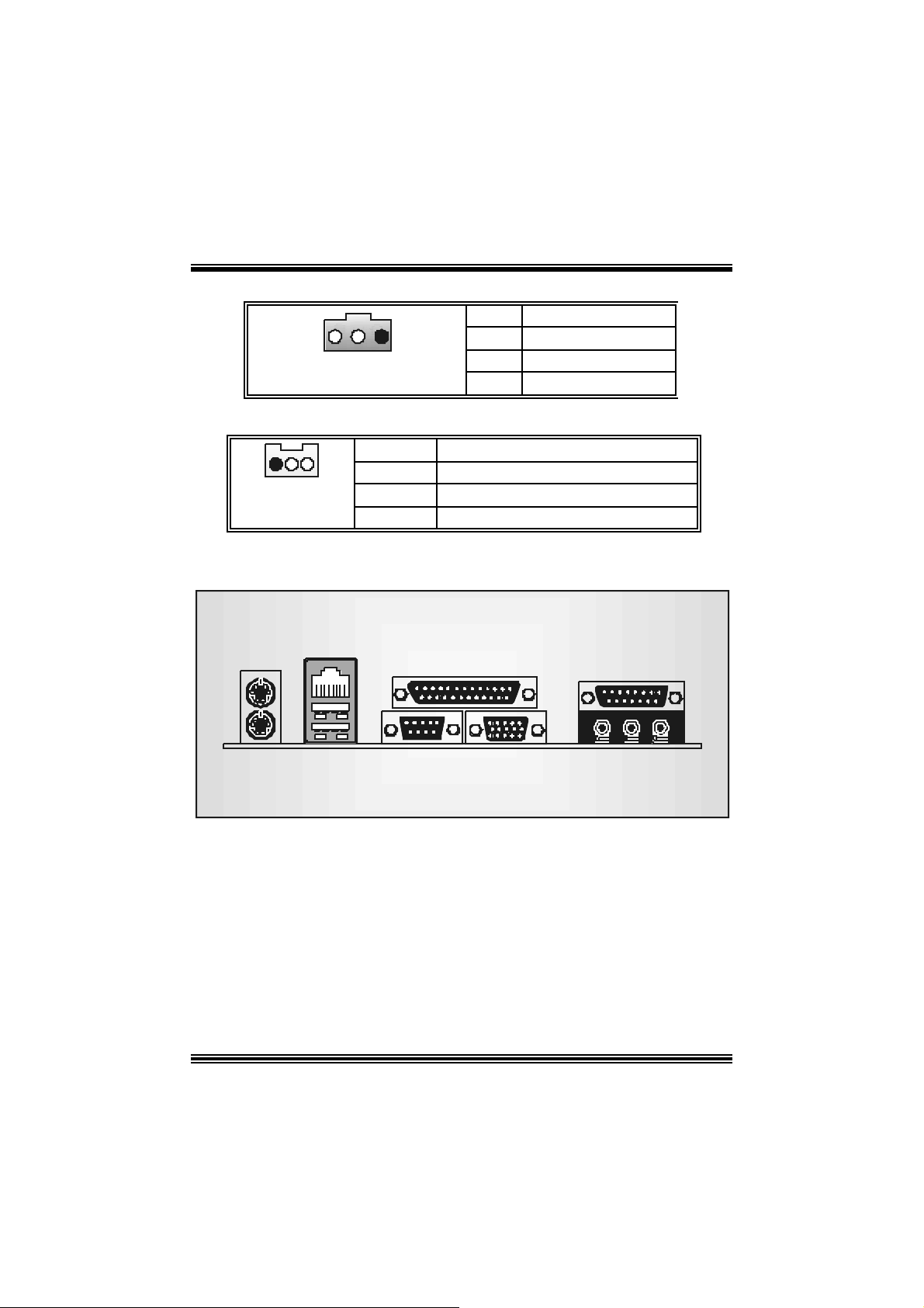
B ack Panel Connectors
JUSBLAN1
PS/2
Mouse
PS/2
Keyboard
JKBMS1
LAN
(Optional)
USB
JCOM1
+5V Standby
Ground
Wak e up
JPRNT1 JGAM E1
Pa rallel Port
COM1
VGA1
Ga m e Port
Speak er
Out
JVGA1
Mic
In
Line In
11

Español
Características del M 6VLQ Pro
A. Har dware
CPU
Pr oporcion a Soc ket 370.
Soporta procesador Celeron™ PPGA (FC-PGA & FC -PGA2) y Pentium® III
Micro-Proc es ador (FC -PGA & F C -PGA2) y VIA C3 Ezra and Ezra –T Samuel 2
para es t aciones de trabajo y serv idores de alta capac idad.
F ront Side Bus a 66/ 100/ 133 MH z.
Chipset
N orth Bridge: VIA CLE266 CE.
Sout h Bridge: VIA VT8235.
Memo ri a Principal
Soport a hasta 2 dis pos it ivos DDR.
Soport a disposit ivos DDR 200/266 MHz (sin ECC ).
Tam año máxima de m emoria 2GB.
Lan Chip (opciona l)
Chip: VI A VT6103.
Soporta 10 Mb/s y 100 Mb/ s aut o-negoc iac ión
H alf / Full duplex.
Ranuras
Tres ranuras 32-bit PC I bus mas t er.
Una ranura C NR.
IDE Onboar d
S opor ta cu atro IDE disk drive s.
Soporta Modo PIO 4, Modo Bride y Ult ra D MA 33/66/100/133 Modo Bus Master.
Super I/O
Chip: ITE IT 8705.
Proporciona el más alt o f uncionam iento de uso común para Super I /O.
Env iro nm ent C ont rol i niti atives
- Monitor H/W
- C ont rolador de Velocidad del Vent ilador
- F unc ión ITE "Smart Guardian"
AC’9 7 Sound Codec O nboard
Chip: VI A VT1612A.
AC ’97 2. 2 S/ PDIF ex t ens ión del codec.
18-bit estéreo full duplex.
12

Periféricos Onboard
a. P art e Tr as era
1 puerto en serie.
1 puerto VGA.
1 puert o parale lo. (m odos SPP/ EP P/EC P)
1 puerto de audio en posic ión horizontal.
1 L AN jack.
R atón PS/2 y tec l a d o PS/2 .
2 p uertos U SB2.0.
b. P ar t e De lantera
1 puerto para dis quetera soportando 2 FDDs de 360K, 720K, 1. 2M, 1.44M y
2.88Mbytes.
4 puertos USB2.0.
1 C onector S/ PDIF Out.
Dimensiones
F orm a de Fac t or Micro ATX: 19 X 24.4cm (W X L)
B. BIOS & S oftware
BIOS
Award legal Bios .
APM1.2.
ACPI.
Función USB.
Software
S oporta Watch dogTM, 9t h T ouc hTM, FLA SHE R™, StudioFun!
Warpspeeder
Ofrec e el más alt o f uncionamient o para Windows 98 SE, Windows 2000,
Window s Me, Window s X P, S CO UNIX etc.
TM
.
TM
(op ci ona l),
Contenido del P a q uet e
Cable HD D X1
Cable FD D X1
Manual del U s uario X1
Cable USB X1 (opcional)
Panel t rasero I/O para carc asa ATX X1 (opcional)
Configuración c omplet a del CD X1
Cable S/PDIF X1 (opcional)
Aplic ac ión del CD StudioF un! X1 (opcional)
13
Cómo instalar un Puente
La ilustración muestra cómo inst alar un puent e. Cuando el Jumper C ap está ubicado en
los contact os , el puente está en “c lose”. Si no hay Jumper C ap ubicado en los contactos,
el puente está en ”open”. La s iguiente ilustración muestra un contacto 3 en el que los
cont actos 1 y 2 est án “close” c uando el J um per Cap est á ubicado en los dos contactos.
Puent e open Puente close Contac to 1-2 close
In stalación de la CPU
Paso 1: Empuje la palanca hacia af uera del socket y levante la palanc a hasta un ángulo de
90 grados .
Paso 2: Fí jese por el punt o blanc o o m árgen cort ado. El punt o blanc o o márgen cortado
debería apuntar hac ia el piv ote de la palanc a. La CPU solament e se fijará en
una sola correcta orient ación.
Paso 3: Tome el CPU firmemente hacia abajo, y cierre la palanca para completar la
instalación.
Paso 4: Ponga el ventilador de la CPU en el CPU y asegúrelo. Conecte el cable de
corriente del v entilador de la CPU al JCFAN1. Ésto completa la instalación.
paso 1 paso 2 paso 3 paso 4
14

Cabezal del Sistema de Ventilación del CPU: JCFAN1
Conrtacto No. Asi gnación
1
JCFAN1
1
2
3
FAN rpm Rate Sense
Tierra
+12V
Cabezal del Sistema de Ventilación: JSFAN1
Contacto No. Asigna ción
13
JSFAN1
1
2 +12V
3
FAN rpm Rate Sense
Tierra
Módu lo s DIMM: D IMM1/ DIMM2
DR AM Tiem p o de Acceso: 2. 5V Un buff e red DDR 200/266 MH z Tipo r equ erido.
DRAM Tipo: 64MB/ 128MB/ 256MB/ 512MB/ 1GB Módulo DIMM (1 84 c ont ac t os)
Tota l del Ta maño de Memoria Unbuf fered DIMMs
Localización
Módu l o DDR T otal del T amaño
del Socket
DIMM
DIMMB1 64MB/128MB/256MB/512MB/1GB
*1
DIMMB2 64MB/128MB/256MB/512MB/1GB
*1
***Solamente para refe rencia***
Instalación del Módulo DDR
1. Abra una ranura de DIMM presionando el clip
de retenc ión hacia afuera. Aliñe el DIMM en la
ranura tales que la muesca en el DIMM encaje
en la c um brera de la ranura.
2. Inserte el DIMM vert icalm ente y f irmem ente en
la ranura hasta que el clip de retención vuelva a
su posición original y el DIMM esté
correctamente colocado.
15
de Memoria (MB)
Máxi mo
2GB
Puen tes, Cabe zales, Con e ct ores y Ran u ras
Conector de Disque tera: FDD1
La placa madre proporciona un conector estándar para disquete que soporta
disquetera de 360K, 720K, 1.2M, 1.44M y 2.88M. Éste conector utiliza cables
proporc ionados por el dis quete.
Conector del Disco Duro: IDE1/ IDE2
La plac a madre tiene un controlador de 32-bit PCI ID E que proporciona Modo PIO
0~5, Bus Master, y func ionalidad Ultra DMA 33/ 66/ 100. Tiene dos conectores
HDD : IDE1 (prim ario) y IDE2 (sec undario).
Los conectores ID E puede conectar a un disco m ast er y uno esc lav o, así puede
conectar hasta cuatro discos duros. El primer disco duro debe estar siempre
conectado al IDE1 .
Ranuras de Interconexión del Componente Pe riférico: PCI1-3
Ésta plac a madre est á equipada c on 3 ranuras estándar PCI. PCI es la sigla para
Interconexión del Componente Perif érico, y es un bus estándar para tarjetas de
expansión. Ésta ranura PCI es tá diseñado con 32 bits.
Ranura de B anda de S uspensión de Comunicación y Red: CNR1
La especificación CNR es una abierta Industria de Arquitectura Estándar, que
def ine una tarjet a de interf ac e escalable del hardware en el que soport a s olament e
modem.
Conectores de Corriente: JATXPWR1
10
20
1
11
JATXPWR1
Contactos Asignación Contactos Asignación
1 +3.3V 11 +3.3V
2 +3.3V 12 -12V
3 Tierra 13 Tierra
4 +5V 14 PS_ON
5 Tierra 15 Tierra
6 +5V 16 Tierra
7 Tierra 17 Tierra
8 PW_OK 18 -5V
9 Voltaje Standby
+5V
10 +12V 20 +5V
16
19 +5V
0
Conector del Panel Frontal: JPANEL1
SLP
JPANEL1
Contacto Asignación Función Contacto Asignación Función
1 +5 V 2 Cont rol de
3 NA 4 Tierra
5 NA 6 NA NA
7 Altavoz
9 HDD LED (+) 10 Corriente LED (+)
11 HDD LED (-)
13 Tierra 14 Botón de
15 Control de
Reinicio
17 NA 18 KEY
19 NA 20 KEY
21 +5 V 22 Tierra
23 IRTX
2
123
PWR_LED
(+) (-)(+)
LED
Botón
(+) (-)
HLED
RST
8 Corriente LED (+)
16 Tierra
24 IRRX
SPK
Conector
del Altav oz
de l D isc o Du ro 12 Corrient e LED (-)
de R einicio
Conector IrDA
IRON/ OFF
24
IR
Suspension
Encendido
Botón
de Suspension
Corriente
LED
Botón de
Encendido
Conec t or IrD A
Cabezal Frontal USB: JUSB1/2
Contactos Asignación Contactos Asignación
1
9
1
3
5
7
9
+5V (fused)
USBP4-
USBP4+
Tierra
KEY
2
4
6
8
10
+5V (f used)
USBP5-
USBP5+
Tierra
NA
2
1
JUSB1/2
17

Fue nte de Co rriente Selección para Teclado/ Ratón: JKBV1
JKBV1 Asignación Descripción
1
3
Contacto 1-2 clo se
1
3
Contacto 2-3 clo se
+5 V
Voltaje
Standby +5V
+5V para teclado y rat ón
Ratón PS/2 y Teclado PS/2 son
e ncendidos con un vol taje standb y d e
+5 V
Nota: Para soportar la función “Encendiendo el sistema por medio del
t eclado y r atón” , el jumper cap del “JKBV1” debe se r ubicado en el contacto
2-3.
Fue nte de Co rriente Selección para USB: J USBV1/ JUSBV2
JUSBV1/JUSBV2 Asignación Descripción
1 3
Contacto 1-2 clos e
1 3
Contacto 2-3 clos e
Nota: Para soportar la función “Encendiendo el sistema por medio del
dispositivo USB”, el jumper cap del “JUSBV1/ JUSBV2” debe ser ubicado en
el contacto 2-3 respectivamente.
+5V J U SBV1: 5V para c onect ores USB
ubicados en el puert o JUSBLAN1
JU SBV2: 5V para c onectores USB
ubicado el el puerto JUSB1/2
Voltaje
Standby +5V
JU SBV1: puerto JU SBLAN1
enc endidos con v oltaje standby de 5V
JUSBV2: puertos JUSB1 /2 e ncendido s
con vol taje standby de 5V
18
Puente de Borrar CMOS: JCMOS1
JCMOS1 Asignación
3
1
Cont acto 1-2 C lose
3
1
Contacto 2-3 Clo se
Operación Normal (def ault)
Borra dat os del C MOS
Los siguientes procesos son para reiniciar la
c ontrasena del BIOS. Es importante que siga los
~
siguientes pasos cuidadosamente.
※ Procedimientos para Borrar CMOS:
1. Quite el c able de corriente del AC.
2. Fijar el puente en el “contacto 2-3 c los e”.
3. Espere 5 segundos.
4. Fijar el Puente en el “c ont act o 1-2 c lose”.
5. Encienda AC.
6. R econf igure la cont raseña deseada o borre datos CMOS.
Conector de la Carcasa Abi erta: JCI1
Asignación
Tierra
1
JCI1
Contactos
1
2
Señal de la Carca sa Ab ierta
Cabe zal de Entrada de Audio CD-ROM: JCDIN1/ JCDIN2
4
1
JCDIN1/2
Contactos Asignación
1
2
3
4
En trada del Canal Izquierdo
Tierra
Tierra
En trada de l Canal Der echo
19
 Loading...