

Page 1

1
Applicable Country & Regions: Europe
Service Manual for BenQ:
LCD E24-5500
(D-SUB + HDMI + Audio + USB +
S-Video+ YPbPr + SPDIF +
SCART + Common Interface +
Black Chassis Colors)
P/N: 9H.V1875.TBE
Product Service Manual – Level 1~2
Version: 1st
Date:12-20-2010
Notice:
For RO to input specific “Legal Requirement” in specific NS regarding to responsibility and
liability statements.
Please check BenQ’s eSupport web site, http://esupport.benq.com
, to ensure that you have the
most recent version of this manual.
First Edition (Dec. 2010)
©
Copyright BenQ Corporation 2010. All Right Reserved.
Page 2

2
Content Index
Abbreviations & Acronyms ........................................................................................................................................ 3
1. About this Manual ................................................................................................................................................... 5
1.1 Important ............................................................................................................................................................ 5
1.2 Trademark .......................................................................................................................................................... 5
2. Introduction ............................................................................................................................................................. 6
2.1 RoHS (2002/95/EC) Requirements – Applied to all countries require RoHS. .................................................... 6
2.2 Safety Warning and Notice ................................................................................................................................. 6
2.3 Compliance Statement ....................................................................................................................................... 7
3. General Description ................................................................................................................................................ 8
4. Related service information ................................................................................................................................... 8
5. Product Overview ................................................................................................................................................... 9
5.1 Monitor Specifications ........................................................................................................................................ 9
5.2 Packing ............................................................................................................................................................. 11
5.3 Customer Acceptance ...................................................................................................................................... 13
Level 1 Cosmetic / Appearance / Alignment Service ............................................................................................ 15
Visual Inspection & Cleaning .................................................................................................................................. 15
Software/Firmware Upgrade Process .................................................................................................................... 25
Adjustment / Alignment Procedure ......................................................................................................................... 29
Level 2 Circuit Board and Standard Parts Replacement ...................................................................................... 40
Product Exploded View .......................................................................................................................................... 40
Six Angles’ View ..................................................................................................................................................... 42
Product Disassembly .............................................................................................................................................. 43
Assembly SOP ....................................................................................................................................................... 47
Block Diagram ........................................................................................................................................................ 51
Schematic Diagram ................................................................................................................................................ 53
Troubleshooting ...................................................................................................................................................... 71
PCB LAYOUT ............................................................................................................................................................. 77
Appendix 1 – Screw List / Torque ........................................................................................................................... 87
Appendix 2 –CODE LIST: IR ..................................................................................................................................... 88
Page 3

3
Abbreviations & Acronyms
A
ADC Analog to Digital Converter
AFC Automatic Frequency Control: control signal used to tune to the correct frequency
B
BenQ BenQ Corporation
BTSC Broadcast Television System Committee
C
CPU Central Process Unit
CVBS Composite Video Blanking and Synchronization
D
DLP Digital Light Processing / Texas Instruments®
DMD Digital Micro mirror Device
DRAM Dynamic RAM
DVI Digital Visual Interface
DVI-D Digital Visual Interface-digital
DVI-I Digital Visual Interface-Integrated
E
EEPROM Electrically Erasable and Programmable Read Only Memory
F
FLASH FLASH memory
G
G-TXT Green Teletext
H
HDMI High Definition Multimedia Interface, digital audio and video interface
HP Head Phone
I
IR Infra-red
I2C Integrated IC bus
L
LED Light Emitting Diode
LVDS Low Voltage Differential Signal, data transmission system for high
M
MOSFET Metal Oxide Semiconductor Field Effect Transistor
Page 4

4
N
NC Not Connected
NVM Non Volatile Memory: IC containing TV related data (for example, options)
O
OSD On Screen Display
P
PC Personal Computer
PCB Printed Circuit Board (or PWB)
R
RC Remote Control transmitter
RGB
Red, Green and Blue. The primary color signals for TV. By mixing levels of R, G
and B, all colors (Y/C) are
ROM Read Only Memory
S
SDA Data signal on I2C bus
SDRAM Synchronous DRAM
SW Sub Woofer / Software
T
THD Total Harmonic Distortion
V
VGA Video Graphics Array
Y
YPbPr
Component video (Y= Luminance, Pb / Pr= Color difference signals B-Y and R-Y,
other amplitudes w.r.t. to YUV)
Y/C
Video related signals: Y consists of luminance signal, blanking level and sync; C
consists of color signal.
Page 5

5
1. About this Manual
The purpose of Service Manual is to provide a guide line to engineers to repair different models. The appearance
and capability is introduced in this Service Manual. It is better for repair engineer to have a rough idea of this model
through reading the Service Manual. Please do pay attention to the item part of the disassembly when repair the
machine and also do the protection of panel any time. When repairing the circuit board, please follow the
requirement of RoHS and refer to the circuit diagram and repairing process that attached in the Service Manual.
The method of firmware updated, the way of using the menu and some information that may be used when
repairing are also attached in the Service Manual that provide repair engineer various choice.
1.1 Important
Only trained service personnel who are familiar with this BenQ Product shall perform service or
maintenance to it. Before performing any maintenance or service, the engineer MUST read the “Important
Safety Information”.
1.2 Trademark
Page 6

6
2. Introduction
This section contains general service information, please read through carefully. It should be stored for easy
access place.
2.1 RoHS (2002/95/EC) Requirements – Applied to all countries require RoHS.
The RoHS (Restriction of Hazardous Substance in Electrical and Electronic Equipment Directive) is a legal
requirement by EU (European Union) for the global electronics industry which sold in EU and some counties also
require this requirement. Any electrical and electronics products launched in the market after June 2006 should
meet this RoHS requirements. Products launched in the market before June 2006 are not required to compliant
with RoHS parts. If the original parts are not RoHS complaints, the replacement parts can be non ROHS
complaints, but if the original parts are RoHS compliant, the replacement parts MUST be RoHS complaints.
If the product service or maintenance require replacing any parts, please confirming the RoHS requirement before
replace them.
2.2 Safety Warning and Notice
Installation
1. Do not use your monitor under any of the following environmental conditions:
Extremely high or low temperature, or in direct sunlight
Dusty places
Highly humid, exposed to rain, or close to water
Exposed to vibrations or impacts in places such as cars, buses, trains, and other rail vehicles
Near heating appliances such as radiators, heaters, fuel stoves, and other heat-generating items (including
audio amplifiers)
An enclosed place (such as a closet or bookcase) without appropriate ventilation
An uneven or sloping surface
Exposed to chemical substances or smoke
2. Do not block vents and openings by clothes or curtains.
3. Carry the monitor carefully.
4. Do not place the monitor face down on the floor or a desk surface directly. Otherwise, scratches on the panel
surface may occur.
5. Do not place heavy loads on the monitor to avoid possible personal injury or damage to the monitor.
6. Ensure that children do not hang or climb onto the monitor.
7. Keep all packing bags out of reach of children.
Page 7

7
Operation
1. To protect your eyesight, please refer to the user manual to set the optimal screen resolution and the viewing
distance.
2. To reduce eye fatigue, take a break on a regular basis while using the monitor.
Avoid taking either one of the following actions for a long time. Otherwise, burn marks may occur.
Use the monitor in the aspect ratio of 2.35:1, 4:3, or 16:9.
Place a still image (such as an OSD menu, fixed text or image) on the screen.
3. To avoid possible damage to the monitor, do not touch the monitor panel by hand, pen, or any other sharp
objects.
4. Excessively frequent plug and unplug of video connectors (D-sub / HDMI) may cause damage to the monitor.
5. This monitor is designed mainly for personal use. If you want to use the monitor in a public place or a harsh
environment, contact your nearest BenQ service center for assistance.
6. To avoid possible electric shock, do not dissemble or repair the monitor.
7. If a bad smell or an abnormal sound appears to come from the monitor, contact your nearest BenQ service
center for assistance immediately.
Cleaning
1. Ensure that the power is unplugged before cleaning your monitor
2. Use a monitor cleaner and a soft cloth to clean your monitor.
3. Do not use solvents such as alcohol to clean your monitor.
Power
1. To avoid possible damage to the monitor, do not use it in a region where power supply is unstable.
2. Ensure that the power cord is connected to a grounded power outlet before turning on the monitor.
3. Use only the power cord provided by BenQ.
4. Never use a power cord that appears to be damaged or frayed.
5. To avoid possible danger, observe the total electric load when using the monitor with a (multi-outlet) extension
cord.
6. Always turn off the monitor before unplugging the power cord.
2.3 Compliance Statement
Caution: This Optical Storage Product contains a Laser device. Refer to the product specifications and your local
Laser Safety Compliance Requirements.
Page 8

8
3. General Description
This new LCD (Liquid Crystal Display) monitor BenQ E24-5500 offers numerous features and functions, for
example:
LED
Minimal space requirements thanks to slim casing
Optimum ergonomic characteristics (totally distortion-free, excellent picture definition and color purity right into
the corners)
Contrast ratio 3000:1 (Panel) / 20 million:1 (DCR), brightness 250nits
MAX. resolution (1920 x 1080)
Automatic scanning of horizontal frequencies from 30 to 83 kHz and refresh rates (vertical frequencies) from 56
to 76 Hz (absolutely flicker-free)
Digital screen controller with microprocessor for storing 15 different display modes
Freely adjustable color alignment for matching the screen colors to the colors of various input and output devices
Convenient operation via integrated OSD (On-Screen-Display) menu
VESA-DDC compatibility
Plug & play capability
Power management for reducing power consumption when the computer is not in use
This operating manual contains important information you require to start up and run your LCD monitor.
This specification defines the requirements for the 24″ MICROPROCESSOR based Multi-mode supported high
resolution color LCD monitor. This monitor can be directly connected to general 15-pin VGA connector and 19-pin
HDMI connector, also supports VESA DPMS power management and plug & play function.
Additional information
Due to the nature of liquid crystal display (LCD) technology, the picture resolution is always fixed. For the best
display performance, please set the display resolution to 1920 x 1080 pixels with an aspect ratio of 2.35:1, 4:3, or
16:9. This is called “Native Resolution” or maximal resolution - that is, the clearest picture. Lower resolutions are
displayed on a full screen through an interpolation circuit. Image blurring across pixel boundaries can occur with the
interpolated resolution depending upon the image type and its initial resolution.
4. Related service information
This Service Manual contains general information. There are 2 levels of service:
Level 1: Cosmetic / Appearance / Alignment Service
Level 2: Circuit Board or Standard Parts Replacement
Service Web Site
eSupport URL: http://esupport.benq.com
Page 9
9
5. Product Overview
5.1 Monitor Specifications
Display
Backlight type LED
Size 24″
Resolution 1920 x 1080
Brightness (cd/m2) (typical) 250nits
Contrast ratio 3000:1
Dynamic Contrast Ratio 20M:1
Response time 25ms
Color depth/colors 8bits
Viewing angle (up/down/ left/right) 178/178/178/178 degrees
TV tuner system
Analog PAL/SECAM
Digital DVB-T/C
Video
Senseye
• Noise reduction • Flesh tone • ACE •
Dynamic backlight
Aspect ratio
• Normal (4:3) • Zoom1 • Zoom2 (2.35:1) •
Wide (16:9) • Panorama
MPEG Noise Reduction Yes
24P True Cinema (no frequency doubling) Yes
Audio
Sound mode
• Standard
• Music
• Cinema
• Speech
• User
Speaker output 5W x 2
Surround system SRS Trusurround HD
Steady Sound Yes
Features
USB multimedia playback
• JPEG
• MP3 • MPEG-1,2,4 • H.264
HDMI CEC Yes
Teletext 1000 pages
Intelligent Shut Down Yes
Time-Shift Yes
Sleep Timer Yes
Clock Yes
Parental Yes
MHEG-5 Yes
Stand tilt/swivel Tilt only (-7 ~ 17 degrees)
Page 10

10
Input terminals
RF tuner 1
HDMI 2
Composite 1
Component 1
S-Video 1
SCART 1
D-sub (VGA) 1
Common Interface 1
USB 1
PC Audio In 1
Output terminals
Video out No
SPDIF out 1
Headphone jack 1
Power
Power input 100 ~ 240 V
Power consumption <60W
Standby mode <0.5W
Dimensions
Dimensions with stand (W x H x D mm) 587.3mm (W) x 424.7mm (H) x184.9mm (D)
Dimensions without stand (W x H x D mm) 587.3mm (W) x 369.9mm (H) x 45.8mm (D)
Weight with stand (Kg) 6kg
Weight without stand (Kg) 4.3kg
Page 11
11
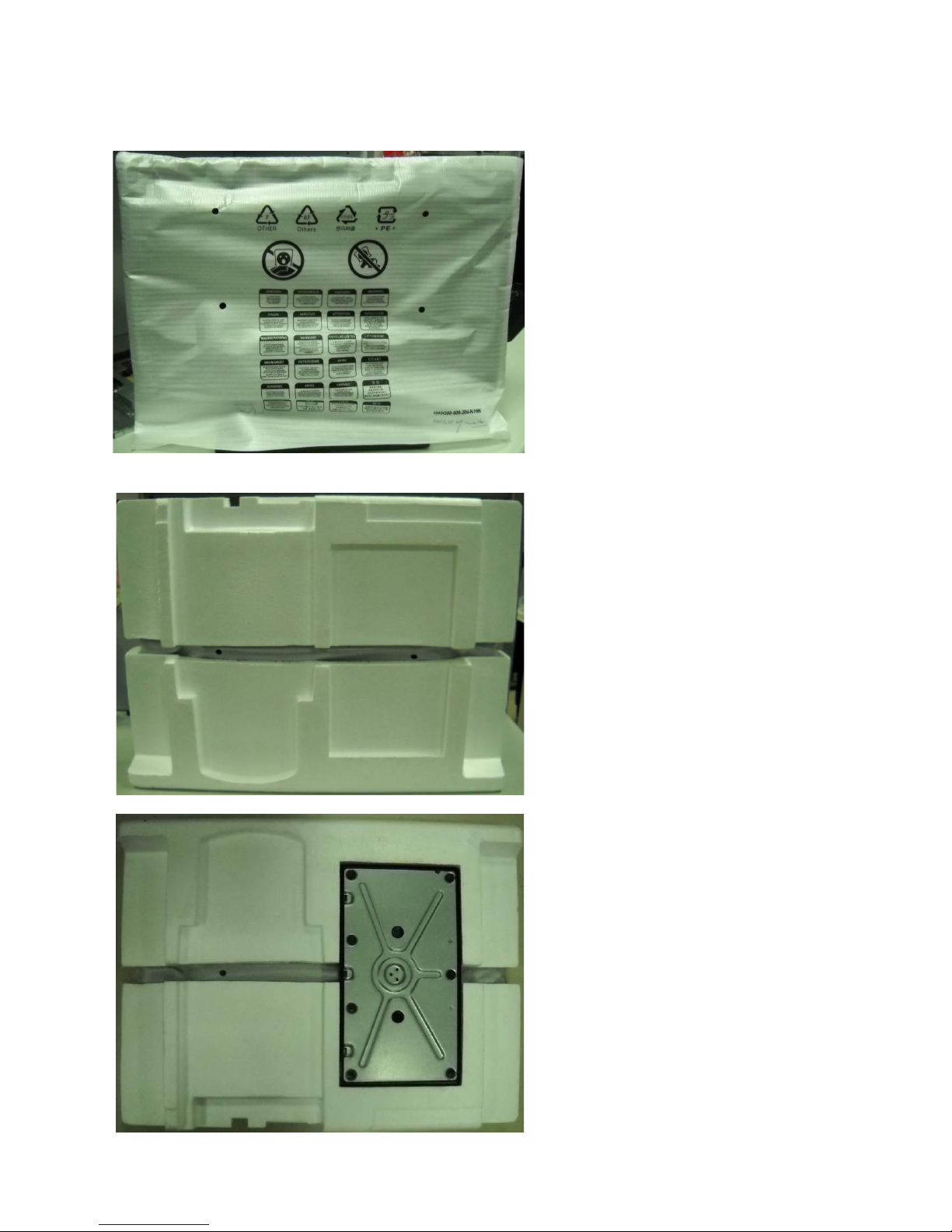
5.2 Packing
When packing the monitor into the carton, please follow the pictures as below.
1. Using the EPE bag to pack the monitor without base
2. Using the EPS to pack the monitor
Page 12
12
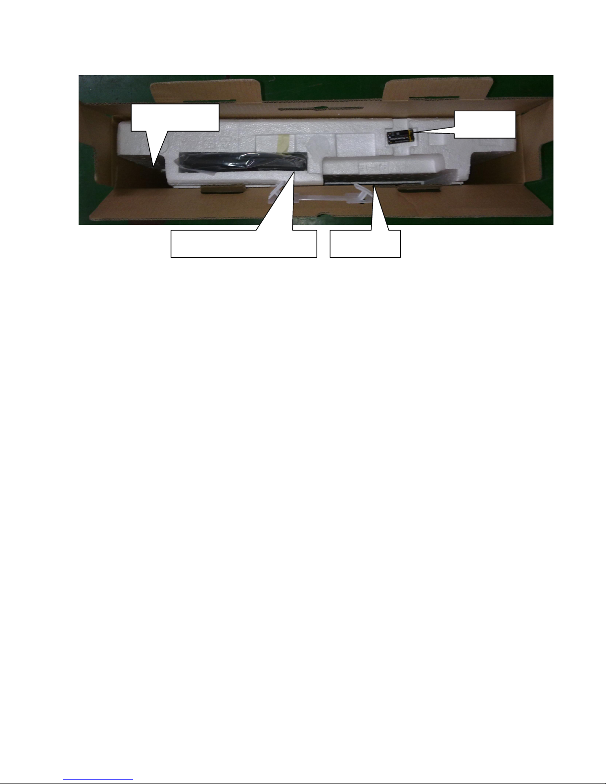
3. Putting the power cord, remote control, screws, battery, and user manual in the position as the picture shows
below.
User manual The remote control and screws
The battery
The power cord
Page 13

13
5.3 Customer Acceptance
E24-5500 (AUO Panel) LCD TV Customer Acceptance Criteria
1.0 SCOPE
This document establishes the general workmanship standards and functional Acceptance criteria for LCD TV
model SV4231 Produced by AUO Inc.
2.0 PURPOSE
The purpose of this publication is to define a procedure for inspection of the LCD TV by means of a customer
acceptance test, the method of evaluation of defects and rules for specifying acceptance levels.
3.0 APPLICATION
The "Customer Acceptance Criteria" is applicable to the inspection of the LCD TV, completely packed and ready for
dispatch to customers. Unless otherwise specified, the customer acceptance inspection should be conducted at
manufacturer's site.
4.0 DEFINITION
The "Customer Acceptance Criteria" is the document defining the process of examining, testing or otherwise
comparing the product with a given set of specified technical, esthetic and workmanship requirements leading to an
evaluation of the "degree of fitness for use", including possible personal injury or property damage for the user of the
product.
5.0 CLASSIFICATION OF DEFECTS
The defects are grouped into the following classes:
5.1 Critical defect
A critical defect is a defect that judgment and experience indicate is likely to result in hazardous or unsafe conditions
for individuals using, maintaining or depending upon the product.
5.2 Major defect
A major defect is a defect, other than critical that is likely to result in failure, or to reduce materially the usability of the
product for its intended purpose.
5.3 Minor defect
A minor defect is a defect that is not likely to reduce materially the usability of the product for its intended purpose, or
is a departure from established standards having little bearing on the effective use of operation of the product.
Note: If BenQ defect undefined failure, and it judged that is reduce the merchandise ability, BenQ CM Inform this
defect. After that parties make communication and decide how to solve.
6.0 CLASSIFICATION OF DEFECTIVES
A defective is a product, which contains one or more defects. The defective will be classified into following classes:
6.1 Major defective
A major defective contains one or more defects and may also contain minor defects but contains no critical defect.
6.2 Minor defective
A minor defective contains one or more minor defects but contains no critical and major defects.
7.0 EXPRESSION OF DEFECTIVES
Number of defects
Percent of defects = ------------------------------------------------ X 100%
Number of products inspected
8.0 INSPECTION STANDARD
Unless otherwise specified, the inspection standard will be defined by MIL- STD-105E (ISO-2859), SINGLE
Page 14

14
SAMPLING PLAN. Level Ⅱ is in use all the time, inspection levels are normal, reduce and tighten.
8.1 Acceptance Quality Level
8.1.1 When a critical defect is found, this must be reported immediately upon detection, the lot or batch shall be
rejected and further shipments shall be held up pending instructions from the responsible person in relevant
organization.
8.1.2
Major Defective: 0.65 AQL
Minor Defective: 1.5 AQL
9.0 GENERAL RULES
The inspection must be carried out by trained inspectors having good knowledge of the meaning of “fitness for use".
The inspection must be based upon the documents concerning the completely assembled and packed product when
more defects appear with the same cause only the most serious defect must be taken into account. Defects found in
accessories packed with the product as connecting cables, plugs, adapters and the like, and being inspected as a
part of the complete product, must be included in the evaluation.
The evaluation must be within the limits of the product specification and, for not specified characteristics, be related
to the design model, limit samples or judgment of a jury of experts. Faults must be demonstrable.
10.0 TEST CONDITIONS
Unless otherwise prescribed, the test conditions are as follows:
. Cold set (switch off for at least 2 hours)
. Nominal mains voltage
. Environmental illumination variable from 500 to 800 Lux (300-500 Lux in Normal I Area)
. Temperature: 24±2℃
. Warm up time: 30minutes minimum.
. Visual inspection shall be down with the distance from eyes to the sample 45 cm.
. Display mode: Primary mode SXGA 60Hz
11.0 TEST EQUIPMENTS
11.1 BenQ PCs with BenQ display adapter or other specific display adapter, which is agreed upon by both parties
11.2 Test program by AUO
11.3 Power saving test tool
11.4 Minolta color analyzer (CA-210)
11.5 Pattern Generator: Chroma
11.6 Fluke or TV signal
11.7 DVD player
11.8 Speaker
Page 15
15
Level 1 Cosmetic / Appearance / Alignment Service
Visual Inspection & Cleaning
Item Description
ID
SPEC
Remark
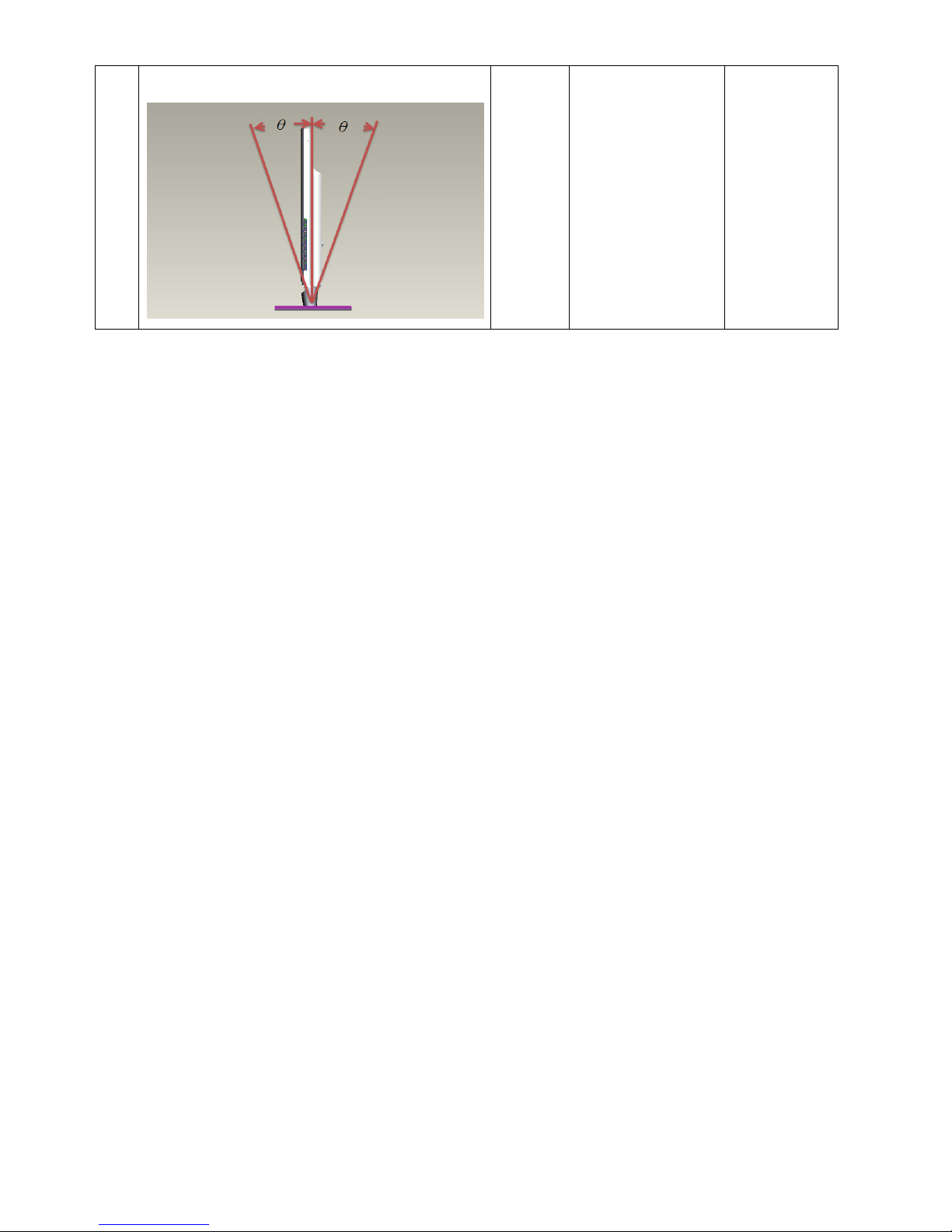
1
Bezel printing
Offset < =0.2mm
Tilt(θ) <= 0.2mm
Offset include
X/Y axis
2
Bezel printing
Offset < =0.2mm
Tilt(θ) <= 0.2mm
Offset include
X/Y axis
3
Component Mylar printing
Offset < =0.2mm
Tilt(θ) <= 0.2mm
Offset include
X/Y axis
Page 16
16
4
Rear cover printing
Offset < =0.2mm
Tilt(θ) <= 0.2mm
Offset include
X/Y axis
5
The height difference with left and right side
5 ARAL
6
machines Twist specifications
3 RL
7
Black side specifications
Shift Tolerance
2.1
2.1
2.1
''
DB
CA
CA
Tilt
0.1
0.1
0.1
0.1
'
'
'
'
DD
BB
CC
AA
Page 17
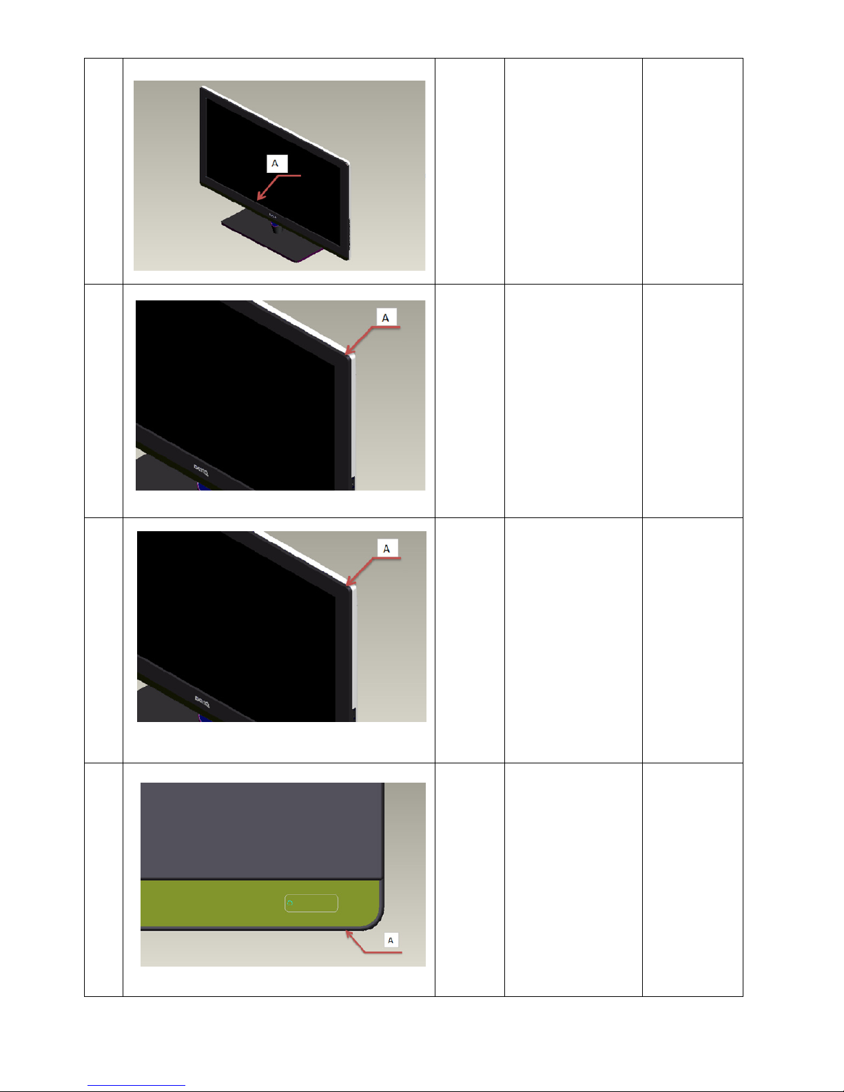
17
8
The gap of the Bezel and Panel
0.1
A
The Gap of the
panel and
bezel must be
symmetrical.
the difference
<= 0.5mm
9
The gap of the Bezel and rear cover
specification A = 0.5
3.0
1.0
AA
10
The STEP of the Bezel and rear cover
5.0
3.0
AA
11
The gap of the Bezel and decorations
ID SPEC Gap = 0.2 mm
2.0
2.0
AA
Page 18
18
12
The STEP of the Bezel and decorations
ID SPEC = 0.0
3.0
1.0
AA
The compages
accords to
bezel template
as a
benchmark.
13
The gap of the Bezel OSD and rear cover
ID SPEC =0.5 mm
2.0
15.0
AA
14
The step of the Bezel OSD and rear
cover
2.0
2.0
AA
The compages
accords to
bezel template
as a
benchmark.
After
compages the
rear cover is
under the
bezel.
15
The gap of the OSD BTN and bezel
ID SPEC =0.3 mm
15.0
15.0
AA
Page 19
19
16
The STEP of the OSD BTN and bezel
ID SPEC = 1.2 mm
2.0
2.0
AA
The height of
the key-press
and bezel
must be evenly
when
assembled the
key-press.
17
The gap of the Rear cover VESA Hole
position
4.0 RL
4.0 BT
18
The gap of the Mylar and rear cover
compages
3.0
RL
AA
3.0
BT
AA
19
The gap of the tuner connector and rear
cover
7.0
RL
AA
7.0
BT
AA
Cable can't
Insert no
bottom
Page 20
20
20
The gap of the component connector and
rear cover
7.0
RL
AA
7.0
BT
AA
Cable can't
Insert no
bottom
21
The gap of the Scart Connector and rear
cover
7.0
RL
AA
7.0
BT
AA
Cable can't
Insert no
bottom
22
The gap specification of the S-Video /
Audio in and rear cover
7.0
RL
AA
7.0
BT
AA
Cable can't
Insert no
bottom
23
The gap specification of the HDMI and
rear cover
7.0
RL
AA
7.0
BT
AA
Cable can't
Insert no
bottom
Page 21
21
24
The gap of the Side HDMI and rear
cover
0.1
RL
AA
4.0
BT
AA
25
The gap of the Side Headphone and rea
r
cover
0.1
RL
AA
0.1
BT
AA
26
0.1
RL
AA
4.0
BT
BB
27
0.1
RL
AA
4.0
BT
BB
Page 22
22
28
The gap of the AC-Socket and rear cover
compages
ID SPEC = 0.5 mm
6.0
RL
AA
6.0
BT
AA
29
The STEP of the AC-Socket and rear cover
compages
ID SPEC
=
E24
=
1.2mm
2.1
2.0
AA
Do not see the
internal bracket
30
The gap of the Hinge Cover and rea
r
cover
Gap Spec A = 0.15 mm
15.0
15.0
AA
31
The Step of the Hinge Cover and rear
cover
Below the template<
0.3
Page 23
23
32
The gap of the aluminum plaque and
stand
Gap Spec A = 0.2 mm
2.0
2.0
AA
33
The STEP of the aluminum plaque and
stand
ID SPEC = 0.5 mm
15.0
15.0
AA
34
Backward force M
3.05.1
Forward force N
3.05.1
35
Machine stress shaking seconds. Time = T
)(6 SECT
Page 24
24
36
degrees of pitch and lean back
00
00
5.15.15:l
5.15.5:p
eanback
itch
Page 25
25
Software/Firmware Upgrade Process
Step 1: Ready for F/W Upgrade
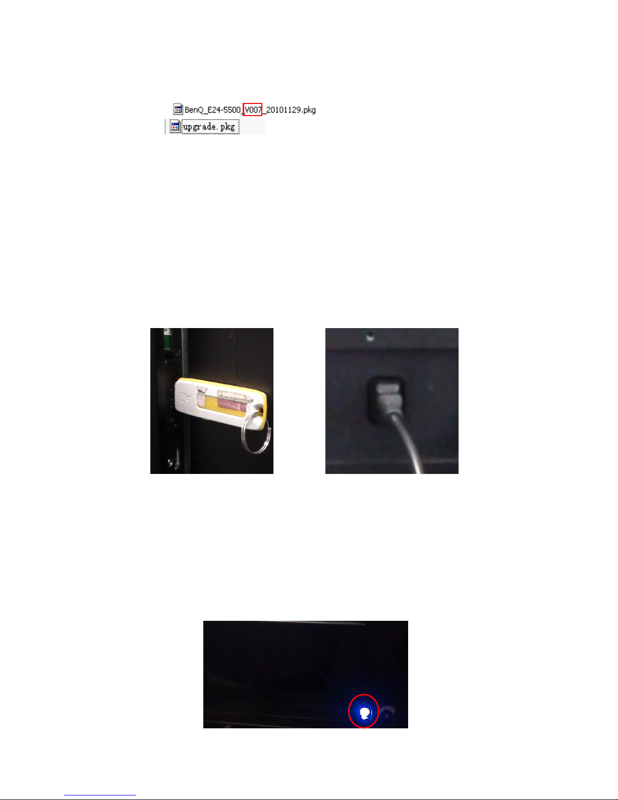
1.1 Change the software file name to ” upgrade.pkg” ,eg:
Before change:
After change:
1.2 Prepare a USB memory (The file system of USB memory must be FAT16 or FAT 32).
1.3 Copy the file (upgrade.pkg) from your computer to the U-disk root path, and remove it from computer’s
USB port!
Note: 1). Note the version of this F/W is V007 before you change the software file name.
2). The software file name must be changed, or TV can’t detect the F/W.
Step 2: F/W Upgrade (There are two methods to upgrade, I will introduce them separately.)
Method 1:
2.1 Plug the USB memory on the USB port on the side I/O port of TV as figure 2.1.
2.2 AC on (Power plug as Figure 2.2)
Figure 2.1 Figure2.2
2.3. After TV monitor AC on, the logo LED color starts to flash as figure2.3, which indicates the TV is upgrading,
forbid to unplug power or U-disk from TV.
Figure 2.3
Page 26
26
2.4. When the monitor screen becomes lights, the upgrade is completed. Unplug the U-disk from TV monitor and
press “power” on remote control or right side power button of TV monitor to restart it as figure2.4.
Figure2.4
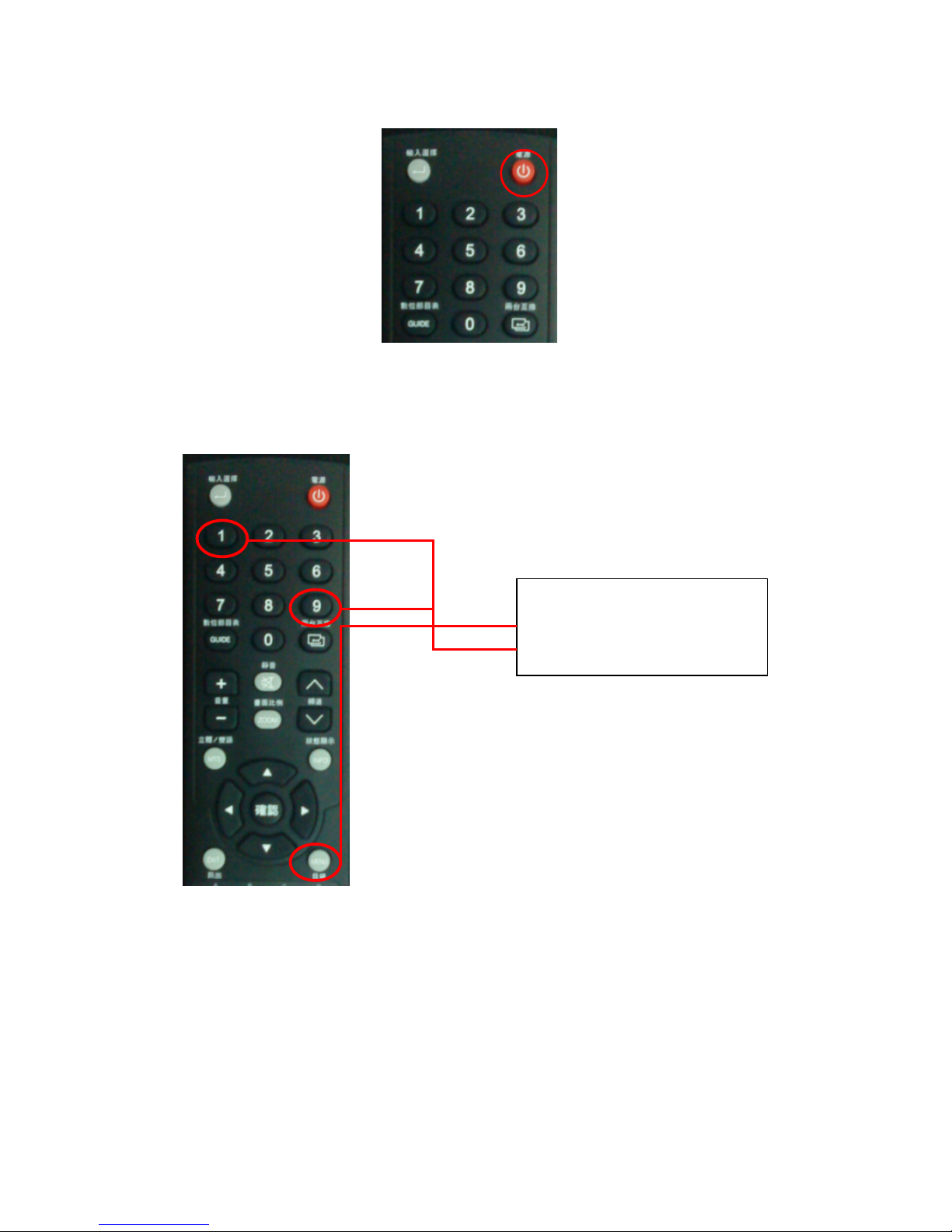
Step 3: Check the F/W version and reset to default.
3.1 Unplug the U-disk. And press “menu+1999” to enter factory model to check whether the TV present FW
Version is the same as the upgrade FW version. Do as the figure3.1.
Figure 3.1
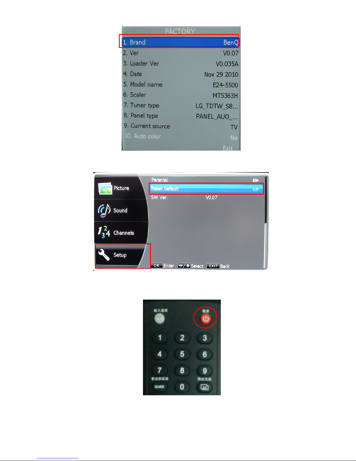
3.2. Check the F/W version on the second item of the factory mode info as figure3.2.
Do the following steps rapidly:
1. Press “MENU”;
2. Press”1”+”9” +”9” +”9”;
Page 27
27
Figure 3.2
3.2 If the FW version is correct, then do factory reset in user menu as figure3.6, else skip to step2 to redo upgrade.
Method 2:
Step1. AC on and turn on TV by remote control or right side “power” button of TV monitor as figure2.1.1.
Figure2.1.1
Step2. Plug U-disk with “upgrade.pkg” file to TV monitor, and it will detect the U-disk as figure2.2.1.
Page 28

28
Figure2.2.1
2.1 Select “YES” and press “ok” to automatic upgrade as figure2.2.2.
Fig2.2.2
2.2 After the progress is 100%, unplug U-disk from TV and enter factory model to check whether the FW version is
correct and do factory in user menu. As to the other details, please refer to the method 1.
Page 29

29
Adjustment / Alignment Procedure
The Control Panel
No. Name Remote Control Description
1 MENU button
Enters or exits the OSD menu.
2
VOL (Volume)
+/- button
• +: Volume up / Navigates to the right
(OSD)
• -: Volume down / Navigates to the left
(OSD)
3
CH (Channel)
▲/▼button
• ▲: Channel up / Moves up (OSD)
• ▼: Channel down / Moves down
(OSD)
4 INPUT button
• Selects an input source.
• In the OSD menu, executes
selections or to enter a submenu you
have selected.
5
Power
Turns on/off the TV.
Page 30

30
Adjusting aspect ratio
The TV can resize and reshape an image to suit your requirements. The visual result depends upon the setting your
have chosen, and the original aspect ratio of the input image. Press Zoom on the remote control to cycle through
different aspect ratios.
Auto Normal 4:3 Wide
Video source
(HD) 4:3
X
Video source
(HD) 16:9
X
Video source
(SD) 4:3
X
Video source
(SD) 16:9
X
Computer
source 4:3
X X
X
Computer
source 16:9
X X
X
Page 31

31
Zoom 1 Zoom 2 Panorama Full Screen
Video source
(HD) 4:3
X X X X
Video source
(HD) 16:9
X X X X
Video source
(SD) 4:3
X
Video source
(SD) 16:9
X
Computer
source 4:3
X X X
Computer
Source 16:9
X X X
• “X” means that the related aspect ratio is not available.
• Available aspect ratio options are dependent on the type of input signal being selected. When the TV is
connected to a computer (via D-Sub or HDMI), only 16:9 and 4:3 are available for selection.
• If the input video signal is in letter box format, select “Zoom” to obtain a wider viewable area.
• To avoid possible “image retention” or “screen burn-in” on the LCD screen of your TV, it is recommended that
you change the aspect ratio from time to time and prevent the TV from displaying a static image for a
prolonged period of time.
• The available menu items are dependent on the input source being selected. Unavailable items will be
grayed out or not displayed.
Page 32

32
Navigating the OSD menu
To enter the On-Screen Display (OSD) menu, press MENU on the remote control or MENU on the TV. Next, follow
the navigation guides shown on the screen bottom.
For example, you can:
1. Press ▲ or ▼on the remote control or CH ▲/▼on the TV to move among 4 different main menus: Picture, Sound,
Channels, and Setup.
2. Press OK on the remote control to enter the submenu of a selected (as highlighted on the screen) menu.
3. Press ▲ or ▼ on the remote control to select an item in the submenu.
4. Press ◄, ◄, ▲ or ▼ on the remote control to adjust settings.
5. Press EXIT on the remote control to return to the previous menu or close the OSD menu (pressing MENU on the
TV closes the OSD menu directly).
See the following section for more information on OSD.
Available menu items may vary depending on the selected input source.
Picture menu
Item Function
Picture Mode
• Vivid: Suitable for viewing in brighter environments. Color, contrast, and brightness of
the image are increased to suit the brighter lighting condition.
• Standard: Suitable for viewing in environments with normal lighting condition. This most
closely represents the broadcast standard quality. No alteration to color, contract or
brightness has been made.
• Cinema: Suitable for viewing movies in darker environments.
Colors have been adjusted to more accurately represent natural skin tones.
• Eco: Saves electricity with low power consumption by providing minimum brightness.
• User: Your own customized picture mode.
Brightness Adjusts the balance between light and dark shades.
Contrast Adjusts the degree of difference between lightness and darkness.
Backlight Adjusts backlight intensity.
Colour Adjusts image color intensity.
Page 33

33
Tint Adjusts color balance.
Sharpness
Adjusts image sharpness level.
When viewing text-rich contents from the VGA or DVI input, you may need to set the
sharpness level to 0 for a suitable display result.
Colour Temperature
Adjusts the color temperature of the black and white part of the image. You can choose
from Normal, Cool, Warm, or User.
Senseye Setting
Adjusts settings in Noise Reduction, Flesh Tone, ACE (Auto Contrast Enhancement),
and Dynamic Backlight.
Picture menu (if connected to a computer via VGA)
Item Function
Brightness Same as above
Contrast Same as above
Colour Temperature Same as above
Auto Configuration Adjusts all related settings automatically by the TV itself.
Position
Adjusts the horizontal and vertical positions of the image in order to center it on the
screen.
Phase Adjusts the display phase to correct shimmering or distortion of the image.
Clock Adjusts the display clock frequency to correct shimmering or distortion of the image.
Sound menu
Item Function
Sound Mode Selects a sound effect.
Equalizer Adjusts sound signals in various frequency ranges.
Treble Adjusts the high tones in sound.
Bass Adjusts the low tones in sound.
Balance
Adjusts the distribution of sounds between the left and the right audio channels of the
built-in speakers, headphone, or SPDIF audio output.
Page 34

34
SRS Surround
Turns on/off the SRS TruSurround HD sound effect, which creates an immersive,
feature-rich surround sound experience from two speakers, complete with rich bass, high
frequency detail and clear dialog.
TV Speaker Turns on/off the built-in speakers.
Digital Audio Out Toggles among Dolby Digital, PCM, and Off.
SPDIF Delay Adjusts the delay time of SPDIF output.
Lip-Sync Sets the delay time of audio output to adjust lip synchronization.
Steady Sound
When Steady Sound is on, it suppresses the possible volume fluctuation between
programming and commercials.
Type
Toggles among Normal, Hard of Hearing (for hearing impaired), and Audio Description
(for visually impaired).
Audio Description Adjusts the volume of Audio Description.
Channels menu
Item Function
Tuner Mode Toggles between two signal sources: Antenna and Cable.
Country Selects the area where this TV is installed.
1st Audio Selects the main audio channel.
2nd Audio Selects the auxiliary audio channel.
Channels
• Channel Scan: Press OK to start automatic channel scanning. All detected channels
will be automatically stored on the TV.
• Update Scan: Scan all channels again to refresh the current stored channel list.
• Signal RF Scan: Used for scanning modulated radio frequency signals.
• Analog Manual Scan: Scans analog TV channels manually.
• Favorites Network Select: Chooses the network you want to watch if more than one
TV network uses the same signal frequency.
• Channel Skip: Omits a selected (already scanned) TV channel.
• Channel Sort: Decides the order of how all scanned channels are displayed.
Page 35

35
• Channel Edit: Customizes the number and name of a channel.
• Decoder: Decides what channels to use if these channels are from a set-top box
connected to the TV via SCART.
• Analog CH Fine Tune: Manually adjusts the frequency used by a channel.
• Clean Channel List: Removes all scanned channels.
Setup menu
Item Function
Menu Language Selects the language for the OSD menu.
Picture Format
Toggles among different aspect ratios: Auto, Normal, Zoom1, Zoom2, Wide, and
Panorama.
• Zoom 1 sets the TV screen image to 14:9 (the screen image is also cut off by 3% from
the top and the bottom respectively).
• Zoom 2 sets the TV screen image to 16:9 (the screen image is also cut off by 13% from
the top and the bottom respectively and by 3% from the left and the right respectively).
• When a computer is connected, only two picture formats (Full Screen and 4:3) are
available.
Time Sets the local date and time depending on your time zone.
Sleep Timer
Sets the timer for the TV to automatically enter the standby mode.
To quit the standby mode, press the Power key on the remote control.
SCART Toggles among different signals when SCART is in use.
Subtitle Sets what text translations are displayed.
Teletext Language Selects the language for Teletext.
Common Interface Displays the status and information when Common Interface is in use.
Auto (CEC) Turns on/off automatic CEC (Consumer Electronics Control) when HDMI is in use.
OAD
Turns on/off OAD (Over Air Download). When OAD is on, updated service or firmware
upgrade can be done.
HDMI Mode Toggles among different HDMI timing modes: Auto, Graphic, and Video.
Page 36

36
HDMI Scan Info
Sets underscan or overscan info to avoid possible black border on the screen when
HDMI is use.
Shop
• On: sets to the Shop mode.
• Off: sets to the Home mode (less power consumption).
E-sticker Displays BenQ TV features.
Demo
When the Shop mode is on, turning on the Demo mode displays a second screen
showing color enhancement effects.
Parental
Helps concerned parents control the access (such as limited time and channels) to the
TV.
Reset Default
Restore all settings to their default values.
The TV channel memory will not be cleared. That is, you do not need to scan and
store the TV channels again after reset.
Software Version Displays the current TV firmware version information.
Available OSD options may vary depending on the model you purchase and may be changed for further
improvement without prior notice.
Time-shift
Time-shift is a convenient tool for you to record the current program shown on TV if you need to be away from the
TV for a while:
1. While you are watching a digital TV channel, plug a USB device into the USB port of the TV.
2. Press
on the remote control to start Time-shift recording. If this is the first time you use the USB device,
the TV will perform the following tasks (please follow the on-screen instructions):
• Detects whether the available empty space is more than 1GB and the USB transmission speed is at least 5. 0
MB/sec.
• Formats the USB device at your choice. If you choose not to format the USB device, all current data on the USB
device will not be removed.
3. If all the above conditions are met, the TV will then start time-shift recording automatically.
4. Once you are back, press
to start time-shift playback. You can press ◄or► on the remote control to fast
rewind/forward at the speed (2X, 4X, 8X, 16X, or 32X). (Press
to resume playback.). Also, you can press
/ to move forward/backward playback a little.
5. To exit time-shift playback, press
. Note that all recorded videos will be automatically removed from the USB
device.
• The USB device must be in the FAT32 file system. Plus, transmission speed of the USB device must be at
least 5.0 MB/sec and the available empty space should be at least 1 GB.
• Once the USB device is full during time-shift recording, time-shift recording will stop automatically.
Viewing images/videos or listening to the music
If you have images, videos, or music stored in a USB device, you can view/ listen to them on the TV:
Page 37

37
1. Turn on the TV, and then plug a USB device into the USB port of the TV.
2. Repeated press Input on the remote control until USB is selected. A folder view of the USB device will then
display on the screen.
3. Press
on the remote control to select a media type: Photo, Music, or Video.
4. Press
and to select other options (such as effects) as needed.
5. Press ◄, ►, ▲ or ▼on the remote control to move to a file you wish to start and press
on the remote
control. All files will automatically be played backed in a sequence.
The USB external storage device must be in the FAT32 file system.
Hotel Mode (Menu + 100108)
Note: When there is any change from OSD settings, the system need to be DC rebooted
Function Option
Power key lock Default
Maximum volume Default
Volume fixed Default
Volume fixed level 30
Remote control enable Yes
Keypad control enable Yes
MENU key enable Yes
Input mode start Default
Input mod fixed Default
Hotel mode off
Reset
Exit
Copy Settings To SUB Press
Copy Settings To TV Press
Factory Mode (Menu + 1999)
Brand BENQ
Main-MCU Ver V0.01
Ver V0.11
Loader Ver V0.029A
Date Dec 31 2010
Model name E24-5500
Scaler MT5363H
Tuner type LG_TDTW_S8…
Panel type PANEL_AUO…
Current source VGA
Auto color NO
ADC R Gain 83
Page 38

38
ADC G Gain 82
ADC B Gain 79
ADC R Offset 113
ADC G Offset 109
ADC B Offset 100
Color temp Cool
Scaler R Gain 77
Scaler G Gain 107
Scaler B Gain 128
Scaler R Offset 125
Scaler G Offset 125
Scaler B Offset 125
Burn in No
EEPROM Init. Press
Back LIT time 131Hr
BlackLight Max 0
BlackLight Max 196
Language English
Preset Press
OAD Enable Yes
VGA Switch EDID
BAUD RATE 115200
VGA UART DISABLE
EFUSE ENABLE
Rotate Screen DISABLE
Up Sync SPK 0
Up Sync HP 0
Up Sync SPDIF 0
ORT mode LAST_STATUS
Gamma ENABLE
DFM MODE No
Exit
Page 39

39
Supported HDMI video timing
Timing Resolution
Horizontal Freq.
(kHz)
Vertical Freq.
(Hz)
Pixel Freq.
(MHz)
Note
480i 720 x 480 (1440 x 480) 15.735 60i 27 HDMI & DVI
576i 720 x 576 (1440 x 576) 15.625 50i 27 HDMI & DVI
480p 720 x 480 31.47 60p 27 HDMI & DVI
576p 720 x 576 31.25 50p 27 HDMI & DVI
720p60 1280 x 720 45.00 60p 74.25 HDMI & DVI
720p50 1280 x 720 37.50 50p 74.25 HDMI & DVI
1080i60 1920 x 1080 33.75 60i 74.25 HDMI & DVI
1080i50 1920 x 1080 28.13 50i 74.25 HDMI & DVI
1080p60 1920 x 1080 67.5 60p 148.5 HDMI & DVI
1080p50 1920 x 1080 56.25 50p 148.5 HDMI & DVI
1080p24 1920 x 1080 27 24 74.25 HDMI
1080p25 1920 x 1080 28.125 25 74.25 HDMI
1080p30 1920 x 1080 33.75 30 74.25 HDMI
Supported computer (D-sub/VGA) input signal resolutions
Resolution Horizontal Freq. (kHz) Vertical Freq. (Hz) Pixel Freq. (MHz) Note
640 x 480 60 31.5 25.7 VESA
640 x 480 72 37.86 31.50 VESA
640 x 480 75 37.5 31.5 VESA
720 x 400 70 31.469 28.322 VESA
800 x 600 60 37.9 40.00 VESA
800 x 600 72 48.08 50.00 VESA
800 x 600 75 46.9 49.50 VESA
1024 x 768 60 48.4 65.00 VESA
1024 x 768 70 56.48 75.00 VESA
1280 x 720 60 44.77 74.50
1280 x 800 60 49.70 83.5
1280 x 1024 60 64.0 108.00 VESA
1366 x 768 60 47.712 85.5 VESA
1440 x 900 60 55.935 106.5 VESA
1680 x 1050 60 65.29 146.25 VESA
1920 x 1080 60 67.5 148.5
• Resolutions outside of these tables are not recognized and will not be displayed.
• When you connect the TV to a computer, you should adjust the resolution in the display properties of the
computer to closely match the native resolution of the TV. For example, 1920×1080@60Hz.
Page 40

40
Level 2 Circuit Board and Standard Parts Replacement
Product Exploded View
Note: The parts information listed below are for reference only, and are subject to change without notice. Please
go to http://cs.tpv.com.cn/hello1.asp
for the latest information.
Item Description Qty Unit
1 DECO L24WTV-TBENQ4 1 PCS
2 LOGO BENQ 1 PCS
3 BEZEL L24WTV-TBENQ4 1 PCS
4 SPEAKER 1 PCS
6 PANEL 1 PCS
7 IR BOARD 1 PCS
9 KEY 1 PCS
10 KEY BOARD 1 PCS
12 MAIN BOARD 1 PCS
13 POWER BOARD 1 PCS
15 MAIN_FRAME 1 PCS
16 INSULATING SHEET 1 PCS
17 REAR COVER 1 PCS
18 BKT-VESA 1 PCS
19 IR LABEL 1 PCS
20 COVER-HINGE 1 PCS
Page 41

41
21 HINGE 1 PCS
23 DECO L26WTV-TBENQ4 1 PCS
24 STAND L26WTV-TBENQ4 1 PCS
26 BASE L26WTV-TBENQ4 1 PCS
27 PLATE_BASE 1 PCS
32 FOOT PAD 1 PCS
33 SHEET 1 PCS
SCREW
Item Part No. Description Qty Unit
5 0Q1G1040 6120 SPEAKER & BEZEL 4 PCS
8 0D1G1030 8120 IR BOARD & BEZEL 1 PCS
11 0D1G1030 8120 MAIN BOARD & MAINFRAME 4 PCS
14 0M1G1740 6120 POWER BOARD & MAINFRAME 1 PCS
22 0M1G1740 10225 CR3 HINGE & REAR COVER 4 PCS
25 0Q1G 130 6120 STAND & HINGE 1 PCS
28 0Q1G 130 6120 PLATE_BASE & BASE 8 PCS
29 0M1G1140 12125 STAND & BASE 3 PCS
30 0M1G 930 6 47 CR3 HDMI & MAINFRAME 1 PCS
31 0M1G 930 8120 HINGE BKT & BEZEL 2 PCS
34 0M1G 130 6 47 CR3 HDMI & REAR COVER 2 PCS
35 0Q1G 930 8 47 CR3 MAIN BOARD & REAR COVER 3 PCS
ART.
Part No. Description Qty Unit
Q44GK044101 EPS 1 PCS
Q44GK044201 EPS 1 PCS
Q44G6000 491A CARTON 1 PCS
Page 42

42
Six Angles’ View
Page 43

43
Product Disassembly
1) Remove the base
Place the monitor face down on a smooth surface. Be careful to avoid scratch and injury during the process of
uninstall. And then remove the base.
2) Remove the stand
Remove the hinge cover and the screws in red to remove the stand.
Pls use a little force when remove
the hinge cover by hand.
Note: If you can’t remove it, you can
use flathead screwdriver (push
down along the direction of arrow),
but you must be careful.
Page 44

44
3) Remove the rear cover
Remove the rear cover as follow:
Note: The BEZEL CLIP is easy to break.
Page 45

45
4) Remove the key board, IR board and speakers from the bezel; remove the main frame from the panel.
5) Remove the boards from the main frame.
Note: The KEY CLIP is easy to break.
Page 46

46
6) The panel
7) The Bezel.
Page 47

47
Assembly SOP
1) Stick the non-woven fabric on the mainframe.
2) Assemble the main board, power board and FFC wire.
Page 48

48
3) Stick the non-woven fabric and Mylar on the panel.
Note: Non-woven Fabric needs to stick from the front of panel metallic edging which couldn’t be
exceeded; And Non-woven Fabric need to be smoothed up and stuck in prison.
4) Assemble the bezel and the panel.
Note: Put the wire on the panel. Don’t pin it.
Non-Woven
Fabric
Page 49

49
5) Assemble the mainframe on the panel. Insert the pin and tidy the wire.
6) Assemble the rear cover.
Stick the non-woven fabric on the rear cover.
Lock the rear cover.
Page 50

50
7) Assemble the hinge.
8) Assemble the base.
9) Assemble the hinge-cover.
Page 51

51
Block Diagram
Main Board
Page 52

52
Power Board
Converter Board
EMI filter
Start Resistor
(R905,R908,R909)
PWM Control
(IC901)
Transformer
AC input
5V
Bridge
Rectifier
and Filter
Feedback
Circuit
Rectifier
diodes
Power Switch
(Q901)
Photo coupler
(IC902)
16V
D801
LED
(CN804)
PWM Control
MP3389EF
(U801)
16V
DIM
ON/OFF
L801
Page 53

53
Schematic Diagram
Main Board
715G3988M0D001005K
FB702 120R/3000mA
1 2
R735
24K1/16W
PWR_5V_13,8, 11,13
PWR_16V_1
R710
NC
DV33SB
C4209
100N 50V
R4303
NC
R708
10K+-5%1/16W
U751
IC G903T63UF 0.6A/3.3V SOT-223
3 2
1
4
VIN VOUT
GND
4
SMD
2.3A
INVERTER_ON_OFF14
C701
NC
POWER_DETECT
+
C702
470uF 16V
﹁
0603
MPS
C765
10U 16V
C767
10U 16V
C720
10N 50V
+5V_SW3,4,6,9,11, 12,13,14
INVERTER_ON_OFF
FB4203120R/3000mA
1 2
Q705
NC
3
1
2
C4210
NC
C704
10N 50V
+16V
R711
56K 1/16W
FB4204 120R/3000mA
1 2
R4306
100K1/16W
MCU_5V_POWER_ON15
C712
1UF16V
C719
10U 16V
PWR_5V15
Q704
AO4411
123
4
876
5
SSS
G
DDD
D
STAND_BY
C732
1uF 25V
PWR_5V_1
FB705
220R/2000mA
12
C735
100N 16V
R731
0R05 1/10W
R729
56K 1/16W
R721
10.2K 1/10W
DV333,4,5,6,8,9,10 ,12,13,14
R4308
NC
R705
22K1/16W
C705
100N 50V
R4309
NC
DV115
R724
22K1/16W
POWER_DETECT9
R725
NC
R713
NC
PWR_5V_1
Q706
LMBT3904LT1G
3
1
2
R4304
4.7K1/16W
Q1157
NC
123
4
876
5
SSS
G
DDD
D
C718
1500P50V
OPWRSB8
C716
NC/180P 50V
PWR_5V_1
R733
10K 1/10W
PWR_5V_1
FB701120R/3000mA
1 2
DV33SB8,12, 13,15
Q702
LMBT3904LT1G
3
1
2
BRIGHT_ADJ14
D701
NC/SS3P4
1 2
PWR_5V_1
POWER_ON
C708
100N 16V
CN701
CONN
1
2
3
4
5
6
7
8
9
10
R720
4K12 +-1% 1/10W
PWR_5V
PWR_16V
C707
100N 16V
PWR_5V
R718
3.3K 1/16W
OPWRSB
+16V13
R730
10K 1/10W
POWER_ON8,15
PWR_16V_13,13
C4211
NC
PWR_5V_1
U701
MP9403EN-LF-Z
1
2
3
4 5
6
7
8
9
BS
IN
SW
GND FB
COMP
EN
SS
Therm al Pad
Q1158
NC
3
1
2
PWR_16V_1
DV11
R4310
NC
1
Custom
114Thursday, December 16, 2010
715G3988M0B0010050
01. POWER-1
G3988-M0B-001-0050-2-101216
OEM MOD EL Size
Rev
Date
Sheet
of
TPV MODE L
PCB NAME
称爹
T P V ( Top Victory Electronics Co . , Ltd. )
Key Component
絬 隔 瓜 絪 腹
PWR_5V
C4212
NC
+5V_SW
C717
100N 16V
R736
100K1/16W
STAND_BY9
BRIGHT_ADJ
R728
4.7K1/16W
R4305
10K+-5%1/16W
R4311
NC
PWR_16V_1
C709
1UF16V
SMD/0402
R714
4.7K1/16W
L701
15uH
C715
100N 16V
PWR_5V_1
+
C4208
330uF 35V
+
C713
470uF 16V
confirm function_Jason
+16V
Q707
AO4411
123
4
876
5
SSS
G
DDD
D
C731
1uF 25V
R4312
NC
DV11
GMT
0.6A
SOT223
MCU_5V_POWER_ON
R4307
NC
Page 54

54
PWR_5V_1
+
C714
100uF25V
R751
10K+-5%1/16W
1
Custom
214Friday , Novem ber 05, 2010
715G3988M0B0010050
02. POWER-2
G3988-M0B-001-0050-2-101105
OEM MOD EL Size
Rev
Date
Sheet
of
TPV MOD EL
PCB NAME
称爹
T P V ( Top Victory Electronics Co . , Ltd. )
Key Component
絬 隔 瓜 絪 腹
PANEL_VCC14
FB4215 N C/120R/3000m A
1 2
C436
1UF16V
0603
C724
1UF16V
PANEL_PWR
C764
10U 16V
C758
10U 16V
D703
NC
DV18_DDR7
D702
NC
+5V_SW2,4,6,9, 11,12,13,14
U753
3 2
1
VIN VOUT
GND/AD J
Q750
AO4411
123
4
876
5
SSS
G
DDD
D
+
C721
470uF 16V
PWR_16V_12,13
D705
RGP15D
R756
120R 1% 1/10W
AV33
+5V_TUN ER
R719
56R 1/10W 1%
C761
1UF16V
+
C753
100UF 16V
C759
100N 16V
C754
100N 50V
FB4213 120R/3000mA
1 2
PANEL_PWR
DV18_DDR
C4214
100N 16V
C763
1UF16V
DV33
R758
NC
R757
1R 1%
4.95
R753
4.7K1/16W
DV33SB2, 8,12,13,15
+
C752
100UF 16V
R750
22K1/16W
1104
PANEL_VCC
R755
56K 1/16W
D704
RGP15D
PANEL_VCC_ON/ OFF
FB4214 120R/3000mA
1 2
Q751
LMBT3904LT1G
3
1
2
FB752
220R/2000mA
1 2
U702
G1084T43Uf
23
1
VOUTVIN
ADJ
R717
120R 1% 1/10W
U75 4
SC4215HSETRT
1
2
3
4
8
7
6
5
9
NC
EN
VIN
NC
GND
FB
VO
NC
TH1
C711
10U 16V
C4213
100N 16V
AV12
AV336,12,14
FB4216 N C/120R/3000m A
1 2
U750
G1117-33T43UF
123
ADJ(GND)
VOUT(TAB)
VIN
FB751
NC/220R /2000mA
1 2
+
C755
100uF 16V
R761
5K1 1/10W 1%
PANEL_VCC_ON/ OFF6
U752
G1117-33T43UF
123
ADJ(GND )
VOUT(TAB)
VIN
PANEL_PWR
R760
43K 1/10W 1%
R759
2.4K 1/10W
AV124,5,6, 7,12,14
C722
10U 16V
+5V_SW
PWR_5V_12,8,11,13
+
C762
100UF 16V
1104
PWR_16V_1
DV334,5,6, 8,9,10,12,13, 14
1%
R765
10K+-5%1/16W
伦猾
6.3x5.5 SMD
105 2000hr
+5V_TUN ER4
DV33
C757
NC/10U 16V
FB706
220R/2000mA
12
Page 55

55
CI_IND ATA1
CVBS0P
R1036
NC/4.7K1/16W
C1041
100N 16V
DV33_DVBC
GND_Tuner
CI_INDATA69
R1011
300R
C1006
30PF 50V
R1017
0R05 OHM
R1018
0R05 OHM
GND_Tuner
GND_Tuner
FAT_IN-6
CI_INSYNC9
CI_INDATA09
R1005
10K+-5%1/16W
TCK_19
DV12_VADC
FB1002
120R/3000mA
1 2
TU102
NC/TUNER
1
2
3
4
5
6
7
8
9
10
11
12
13
14
15
16
17
18
19
20
21
22
23
24
252627
28
RF Pin In/Out
Ant Pwr
GND
NC
RF AGC
GND
VP(TUN)
VT
GND
NC
AS
SCL
SDA
NC
IF_AGC
DIF1
DIF2
WIF OUT
NC
NC
NC
NC
NC
NC
TH1
TH2
TH3
TH4
TP1000
1
CVBS0P6
TU_FAT_IN2-_T
TVAVLID
C1039
100N 16V
C1034
100N 16V
C1028
NC/10N 16V
+5V_T1
C1040
10U 16V
R1016
NC/4.7K1/16W
+5V_SW
TUNER_CLK_Demod
TUNER_DATA_Demod
MPX_N
RP1002
0OHM 1/16W
1
2
3
4
8
7
6
5
RF_AGC_NXP
C1036
100N 16V
RF_AGC_TUNER9
MPX_P6
CI_INSYNC
R1049
51R 1%
R1030
NC/100R 1/ 16W 5%
TUNER_CLK
C4235
10U 16V
TSYN C
+5V_TUNER3
+5V_TUNER
GND_Tuner
U101
Si2163
123456789
10
29
30
31
33
32
34
35
36
282726252423222120
19
11
12
13
15
16
17
14
18
37
GND
AGC_IF
AGC_RF
SCL_HOST
SDA_HOST
VDD_CORE
TS_VAL
TS_SYNC
TS_CLK
GND
ADC_IP
ADC_IN
ADC_CP
SDA_MAST
ADC_CN
SCL_MAST
RESSI_ADC
GPIO_0
VDD_VADC
VDDH_ANA
ADDR
XTAL_I
XTAL_O
VDD_VCORE
RESETB
TS_ERR/GPIO_2
TS_DATA7
GND
TS_DATA0
TS_DATA1
TS_DATA2
VDD_HVIO
TS_DATA4
TS_DATA5
TS_DATA3
TS_DATA6
GND
R1038
NC/0R05OHM1/16W
C1037
100N 16V
FB1014
120R/3000mA
1 2
GND_Tuner
M_AOLRC K5,6
GND_Tuner
TCK_1
R1001
NC/75OHM1/16W
R1006
10K+-5%1/16W
FB1005
120R/3000mA
1 2
TU_FAT_IN2-
L1003
0.33uH 10%
FB1003
120R/3000mA
1 2
C1022
33P 50V
C1013
47N16V
C1026
NC/47pF 50V
TU_F AT_IN 2+_ T
C1005
30PF 50V
X1000
16MHZ 20P
1 2
C1004
100N 16V
FAT_IN-
IF_AGC_C
GND_Tuner
TU_FAT_IN2+
TDO
TUNER_CLK_Demod
R1041 0R05 OHM
C1008
100N 16V
FAT+
C1019 33P 50V
+
C1000
330uF 10V
TDO9
R1010
0R05 OHM
TSYN C
DV33SB2,8,12, 13,15
TU_FAT_IN2+
R1033
10K+-5%1/16W
R1042 0R05 OHM
FB1013 120R /500mA
1 2
CI_INDATA39
C1049
10P 50V
R1002
4.7K1/16W
TUNER_DATA6
LNA_ON/OFF9
IF_AGC
GND_Tuner
TUNER_BYPASS_I n6
T_SC L
DV12_DVBC
RP1000
0OHM 1/16W
1
2
3
4
8
7
6
5
R1037
NC/4.7K1/16W
C1014
47N16V
T_SD A
C1038
100N 16V
R1035
100OHM1/16W
DV112,5
+5V_T1
TU_MPX_P2
GND_Tuner
TUNER_DATA
1
Custom
314Monday, Nov ember 01, 2010
715G3988M0B0010050
03. TUNER
G3988-M0B-001-0050-2-101101
OEM MOD EL Size
Rev
Date
Sheet
of
TPV MODEL
PCB NAME
称爹
T P V ( Top Victory Electronics Co . , Ltd. )
Key Component
絬 隔 瓜 絪 腹
FAT_IN+_C
C1010
39pF 50V
LNA_ON/OFF
MPX_P1
C1012
47N16V
DV33_DVBC
CI_INVALID9
TU_FAT_IN2-
U103
TS5A3157DCKR
1
2
3 4
5
6
NO
GND
NC COM
V+
IN
R1025
0R05 OHM
RP1001
0OHM 1/16W
1
2
3
4
8
7
6
5
C1009
1N 50V
FAT+
TU_FAT_IN2-
FB1004
120R/3000mA
1 2
R1007
10K+-5%1/16W
C1017
220pF 50V
IF_AGCT_T
FB1008
120R/3000mA
1 2
SYSTEM_REST
CI_INVALI D
R1012
300R
AV123,5,6,7, 12,14
RF_AGC
R1028
NC/0R05OHM1/16W
IF_AGC
TUNER_BYPASS_I n
DV333,5,6,8,9,10,12, 13,14
FAT-
FB1001
120R/3000mA
1 2
C1031 100P 50V
DV33_DVBC
C1025
NC/15PF50V
FB1022
120R/3000mA
1 2
CI_IND ATA5
R1047
0R05 OHM
FB1019
120R/3000mA
1 2
R1043
0R05 OHM
FAT-
GND_Tuner
GND_Tuner
TUNER_CVBS1
C1029
NC/1N 50V
SYSTEM_REST9
C1015
47N16V
R1008
10K+-5%1/16W
R1044
0R05 OHM
L1008
NC
TUNER_CLK6
AV12
IF_AGCT
FAT_IN+_C
TUNER_CLK_Demod
R1045
0R05 OHM
Back
TUNER_CVBS1
MPX_P
FB1006
220R/2000mA
1 2
C1003
100N 16V
TVAVLID9
M_AOLRC K
+5V_TUNER
C1021
22P 50V
R1029
NC/100R 1/16W 5%
DV33
CI_IND ATA6
C1001
10U 16V
CI_INDATA79
T_SD A
C1018
33P 50V
IF_AGCT6
CI_IND ATA0
TUNER_DATA
FAT_IN+6
TCK_1
TU101
TUNER
1
2
3
4
5
6
7
8
9
10
11
12
13
14
15
16
171819
20
ANT[+5V]
LNA ON/OFF
GND
+B(5V)
RF AGC
GND
SDA
SCL
TU AS
DIF[+]
DIF[-]
IF AGC
NC
NC
NC
NC
TH1
TH2
TH3
TH4
RF_AGCT
GND_Tuner
R1021
0R05 OHM
CI_INCLK9
TU_F AT_IN 2-_ T
FB1000
120R/3000mA
1 2
TUNER_DATA_Demod
C1011
39pF 50V
R1040
NC/0R05OHM1/16W
L1001
0.22uH 10%
C1097
10N 50V
MPX_N1
L1002
0.33uH 10%
R1023
4.7K1/16W
CI_INDATA19
TU_FAT_IN2+
C1035
100N 16V
DV12_DVBC
R1046
0R05 OHM
DV33_DVBC
R1027
NC/0R05OHM1/16W
C1007
100N 16V
C1046
NC
C4233
10N 50V
GND_Tuner
CI_INDATA29
RF_AGC_NXP
TVAVLID
DV33_DVBC
CI_IND ATA2
RP1003
0OHM 1/16W
1
2
3
4
8
7
6
5
FB1017
120R/3000mA
1 2
R1039
100OHM1/16W
FAT_IN+
CI_IND ATA3
FB1015
120R/3000mA
12
C4232
10N 50V
R1026
NC/0R05OHM1/16W
SMD/0402
TUNER_CVBS
FAT_IN-_C
FB1011
120R/3000mA
1 2
R1000
NC/75OHM1/16W
R1048
51R 1%
R1003
4.7K1/16W
C1002
10U 16V
C4236
100N 16V
FB1023
60 OHM
12
GND_Tuner
IF_AGCT_T
RF_AGC_TUNER
TCK_0
Q1001
NC/BC857C
RF_AGCT6
+5V_SW2,3,6, 9,11,12,13, 14
DV12_DVBC
C1016
220pF 50V
C4234
100N 16V
GND_TunerGND_Tuner
L1000
0.22uH 10%
GND_Tuner
MPX_N6
CI_IND ATA4
TU_FAT_IN2+_T
R1024
NC/100K1/16W
R1034
NC/0R05OHM1/16W
R1019
1K 1/16W
C1042
NC/10P 50V
AV12
TSYN C9
CI_INCLK
TUNER_CLK
T_SC L
IF_AGC_C
C1033
100N 16V
Front
FB1016
120R/3000mA
1 2
GND_Tuner
TDO
TUNER_DATA_Demod
FAT_IN-_C
DV12_VADC
CI_INDATA49
CI_INDATA59
TU_MPX_P2
C1030
NC/1N 50V
FB1012
120R/3000mA
1 2
C1027
NC/10N 16V
CI_IND ATA7
L1005
NC/0.22uH 10%
FB1009
120R/3000mA
1 2
FB1007
120R/3000mA
1 2
C1020
22P 50V
Page 56

56
R4005
4.7K1/16W
C4005
100N 16V
SMD/0402
R4006
4.7K1/16W
AV12
SMD/0402
DV11
FB4000
120R/3000mA
1 2
DV11
C4013
100N 16V
SMD/0402
R4003
4.7K1/16W
SMD/0402 SMD/0402
M_AOL RC K
C4011
100N 16V
C4014
100N 16V
AV123,4,6,7,12,14
DV33
C4001
100N 16V
R4004
4.7K1/16W
M_AOB CK
C4008
100N 16V
R4002
NC/4.7K1/16W
SMD/0402
M_AOSDATA0
Power
&
Ground
U401A
MT5363LIMG
AF29
AG32
AH33
AG30
Y3
J4
L4
W4
J6
L6
W6
C8
E8
G8
AE8
D9
F9
AF9
G10
AB13
AD13
N14
R14
W14
AC14
P15
T15
V15
AB15
U16
W16
AA16
AC16
T17
V17
Y17
AB17
R18
U18
W18
AA18
AC18
T19
V19
Y19
AB19
N20
R20
U20
W20
AA20
AC20
B21
D21
P21
T21
V21
Y21
AB21
AD21
E22
G22
R22
U22
W22
AA22
AC22
AM1
AL2
AN2
AM3
AL4
AN4
AK5
AM5
AJ6
AL6
AH7
AK7
AM7
AJ8
AL8
AG12
V13
Y13
U14
AA14
AE14
Y15
AD15
R16
AE16
AD17
AE18
AD19
AE20
N22
AE22
N24
W24
AA24
T25
V25
H23
J30
H31
V31
W32
W34
W36
AF13
AH29
AH31
P23
T23
V23
Y23
AB23
AD23
R24
U24 AC24
AE24
P25
AD25
Y25
AB25
AF15
AVDD12_TVDPLL
AVDD12_SY SPLL
AVDD12_ADC PLL
AVDD12_APLL
DVSS
DVSS
DVSS
DVSS
DVSS
DVSS
DVSS
DVSS
DVSS
DVSS
DVSS
DVSS
DVSS
DVSS
DVSS
DVSS
DVSS
DVSS
DVSS
DVSS
DVSS
DVSS
DVSS
DVSS
DVSS
DVSS
DVSS
DVSS
DVSS
DVSS
DVSS
DVSS
DVSS
DVSS
DVSS
DVSS
DVSS
DVSS
DVSS
DVSS
DVSS
DVSS
DVSS
DVSS
DVSS
DVSS
DVSS
DVSS
DVSS
DVSS
DVSS
DVSS
DVSS
DVSS
DVSS
DVSS
DVSS
DVSS
DVSS
DVSS
DVSS
DVSS
DVSS
VCCK
VCCK
VCCK
VCCK
VCCK
VCCK
VCCK
VCCK
VCCK
VCCK
VCCK
VCCK
VCCK
VCCK
VCCK
VCCK
VCCK
VCCK
VCCK
VCCK
VCCK
VCCK
VCCK
VCCK
VCCK
VCCK
VCCK
VCCK
VCCK
VCCK
VCCK
VCCK
VCCK
VCCK
VCCK
VCCK
VCCIO33
VCCIO33
VCCIO33
VCCIO33
VCCIO33
VCCIO33
VCCIO33
VCCIO33
AVSS12_PLL
AVSS12_PLL
DVSS
DVSS
DVSS
DVSS
DVSS
DVSS
DVSS
DVSS DVSS
DVSS
DVSS
DVSS
VCCK
VCCK
VCCIO33
DV333,4,6, 8,9,10,12, 13,14
SMD/0402
C4000
100N 16V
M_OPCTRL3
SMD/0402
1
Custom
414Friday , September 10, 2010
715G3988M0B0010050
04. MT5362 BYPASS/TRAP.
G3988-M0B-001-0050-1-100901
OEM MOD EL Size
Rev
Date
Sheet
of
TPV MODEL
PCB NAME
称爹
T P V ( Top Victory Electronics Co . , Ltd. )
Key Component
絬 隔 瓜 絪 腹
M_AOL RC K4,6
M_SPDIF_Out6,11
M_AOBCK6
M_OPW M1
C4004
100N 16V
SMD/0402
R4000
4.7K1/16W
C4006
100N 16V
SMD/0402
SMD/0402
DV112
C4002
100N 16V
M_OPW M19
SMD/0402
C4012
100N 16V
SMD/0402
C4015
100N 16V
SMD/0402
M_SPD IF _Ou t
DV33
SMD/0402
C4007
100N 16V
M_AOSDATA06
SMD/0402
AVDD1V25_PLL
C4010
100N 16V
DV33
C4003
100N 16V
R4001
4.7K1/16W
C4009
100N 16V
M_OPCTRL38,11,12
AVDD1V25_PLL
Page 57

57
1
Custom
514Friday , September 10, 2010
715G3988M0B0010050
05. MT5362 PERIPHERAL/USB2.0
G3988-M0B-001-0050-1-100901
OEM MOD EL Size
Rev
Date
Sheet
of
TPV MODEL
PCB NAME
称爹
T P V ( Top Victory Electronics Co . , Ltd. )
Key Component
絬 隔 瓜 絪 腹
SOY111
GP11
USB_DM
FB4058
120R/500mA
1 2
R4054
4.7K1/16W
HSYNC11,15
M_AOLRCK4,5
Y0P
COM1
RF_AGCT4
Tuner_ByPas s_Out10
AVDD3V3_ADAC0
VSYNC
CN103
CONN
3
2
1
65
4
AVDD3V3_SIF
AV1_R_In
---><---|>
Line_Out_R13
SMD/0402
SMD/0402
SCART1_R_In10
YPbPr_L_In
AVDD3V3_DIG
MPX_N
C4052
100N 16V
FB4057
120R/500mA
1 2
CVBS0N11
HP_Out_L
FAT_IN-
SMD/0402
COM010
C4064
10U 16V
R4056
0R05 1/10W
R4063
0R05 1/10W
C4059
100N 16V
SMD/0402
USB_PWR_OCP9
USB_PWR_EN9
HP_Out_R
CVBS0N
TP4155
1
PB1P11
Audio I/F
MT5363LIMG
U401F
W30
Y29
AA30
Y31
T31
U30
AB33
AD33
V35
Y33
AC32
AC34
V37
AA32
AB31
AE34
U34
Y35
AB35
U32
AE36
AA34
AD35
AF33
U36
Y37
AB37
AF35
V33
AA36
AC36
AF37
AJ30
AK29
AK31
AL30
AM33
AN36
AN34
L32
M37
K31
K33
L34
N32
P35
L36
M35
P37
AVDD33_REF_AADC
AVSS33_REF_AADC
VMID_AADC
AVDD33_AADC
AVDD33_ADAC1
AVSS33_ADAC1
AIN4_R_AAD C
AIN0_L_AADC
AL2
AVSS33_AADC
AIN1_R_AAD C
AIN0_R_AAD C
AL3
AIN4_L_AADC
AIN1_L_AADC
AVSS33_ADAC0
AR2
AIN5_R_AAD C
AIN2_R_AAD C
AL1
AR0
AIN5_L_AADC
AIN2_L_AADC
AVDD33_ADAC0
AR3
AIN6_R_AAD C
AIN3_R_AAD C
AVICM
AR1
AIN6_L_AADC
AIN3_L_AADC
AL0
AVSS33_DIG
AVSS33_SIF
AVDD33_DIG
AVDD33_SIF
AF
MPXN
MPXP
ALIN
AOLRCK
AOSDATA3
ASPDIF
AOBCK
AOSDATA4
AOSDATA1
AOSDATA0
AOMCLK
AOSDATA2
R4060
0R05 1/10W
SY0
C4051
100N 16V
USB_DP12
AV1_L_In
R4053
4.7K1/16W
M_AOSDATA0
COM0
DV333, 4,5,8,9,10,12,13,14
VGA_L_In11
VSYNC11,15
GP
D4050
BAV99
3
1
2
+
C4063
100UF 16V
Monitor_Out_L
TUNER_DATA
Y1P11
Monitor_Out_R
C4069
1uF 16V
USB_DM12
SOY1
CVBS0P4
SMD/0402
PB0P10
AVDD1V25_RGB
VGA_R_In11
PANEL_VCC_ON/OF F3
M_SPDIF_Out
SMD/0402
R4050
560R 1/10W 1%
MPX_N4
U105
G5250M1T1U
1
2
34
5
OUT
GND
OCEN
IN
C4055
100N 16V
SCART1_Out_R10
R4052 0R05 OHM
RP
AVDD3V3_SIF
PANEL_VCC_ON/OF F
YPbPr_R_In11
+5V_SW
DV33
AMP_MUTE13
VGA_R_In
AVDD3V3_ADAC0
AVDD3V3_ADAC1
TUNER_BYPASS_In4
BP11
AV33
Inverter
C4067
1UF16V
AV33
PR1P11
C4068
1uF 16V
SMD/0402
SMD/0402
AV33
IF_AGCT4
R4051 0R05 OHM
TUNER_BYPASS_In
M_AOBCK
C4054
100N 16V
+5V_SW2,3, 4,9,11,12,13,14
PB0P
VGA_L_In
SMD/0402
VIMD_AADC
SMD/0402
AV33
HP_Out_L13
RP11
AV123,4,5,7,12,14
SCART1_L_In10
PR1P
SOG11
AVDD3V3_REFP_AADC
BL_ON/OFF14
C4061
100N 16V
M_SPDIF_Out5,11
FB4060
220R/2000mA
1 2
AVDD3V3_DIG
RF_AGCT
SOY0
TUNER_CLK
Video I/F
MT5363LIMG
U401D
AR32
AN32
AR34
AU34
AP33
AT33
AP35
AT35
AR36
AU36
AM31
AT37
AP37
AG34
AH35
AH37
AG36
AR30
AN30
AM29
AP31
AT31
AR22
AU22
AP23
AT23
AR24
AU24
AP25
AT25
AM25
AR26
AU26
AP27
AT27
AN26
AR28
AU28
AP29
AT29
AU30
N34
M31
M33
N36
AVSS33_CVBS
AVDD33_CVBS
SY1
SC1
SY0
SC0
CVBS2P
CVBS3P
CVBS0N
CVBS1P
BYPASS0
CVBS0P
TUNER_BYPASS
AVDD33_DEMOD1
ADCINN_DEMOD
ADCINP_DEMOD
AVSS33_DEMOD1
AVSS33_VDAC
AVDD33_VDAC
FS_VDAC
VDAC_OUT1
VDAC_OUT2
HSYNC
VSYNC
SOG
BP
COM
GP
SOY1
RP
AVDD12_RGB
COM1
Y1P
PR1P
PB1P
AVSS12_RGB
Y0P
SOY0
PB0P
COM0
PR0P
TUNER_DATA
IF_AGC
RF_AGC
TUNER_CLK
SMD/0402
SMD/0402
AVDD3V3_CVBS
USB_PWR_EN
R4057
0R05 1/10W
SMD/0402
AVDD3V3_VDAC
HP_Out_R13
M_AOLRC K
TP41591
R4058
0R05 1/10W
SMD/0402
Y0P10
ADAC_VCM
BP
TP4050
1
VIMD_AADC
SMD/0402
SCART1_Out_L10
TUNER_DATA4
AMP_MUTE
Line_Out_L13
CVBS3P
C4050
100N 16V
CVBS0P
CVBS1P
AVDD1V25_RGB
AV1_R_In11
SCART1_Out_L
Y1P
C4060
100N 16V
C4057
100N 16V
AVDD3V3_AADC
SOG
MPX_P
SC0
AV33
COM
AV33
AVDD3V3_ADAC1
C4053
100N 16V
AVDD3V3_REFP_AADC
BL_ON/OFF
COM11
SCART1_Out_R
R4055
NC/10K1/16W
TUNER_CLK4
+5V_SW
TX_RX_ON /O FF11
Line_Out_L
R4059
0R05 1/10W
PR0P10
D4051
BAV99
3
1
2
AV333,12,14
HSYNC
YPbPr_R_In
SY011
SOY010
AVDD3V3_VDAC
AV33
SCART1_L_In
PR0P
Tuner_ByPass_Out
MPX_P4
FAT_IN+
R4062
0R05 1/10W
CVBS3P10
COM111
TX_RX_ON/ OFF
C406510U 16V
---><---|>
AV1_L_In11
PB1P
AV33
ADAC_VCM
AVDD3V3_CVBS
TP41601
USB_DP
AVDD3V3_DEMOD
R4061
0R05 1/10W
SCART1_R_In
C4062
1uF 16V
AV12
t
TH4050
NC/PTCR
1 2
AVDD3V3_AADC
SMD/0402
FAT_IN-4
YPbPr_L_In11
C4058
100N 16V
SC011
C4066
100N 16V
61G 56A050 WT
M_AOSDATA05
M_AOBCK5
Line_Out_R
CVBS1P11
AVDD3V3_DEMOD
FAT_IN+4
USB_PWR_OCP
IF_AGCT
C4056
100N 16V
Page 58

58
1_A12
RP4104
56R
1
2
3
4
8
7
6
5
C4104
100N 16V
RBA2
RBA0
RA2
1_ODT
1_A2
1_CS#
RDQ20
RODT
DV18_DDR
RDQM2
RRAS#
RA9
RWE#
RA10
RCLK0
R4108 100OHM1/16W
DV18_DDR
RDQ4
RVREF1
RDQ7
RDQ13
1_A11
C4120
100N 16V
DV18_DDR
RDQS0#
RCS#
RBA01_A12
RCAS#
RBA2
RBA1
1_ODT
+
C4102
NC/100uF 16V
R4104
1K1/10W
C4116
1uF 16V
RA2
RDQ31
RDQ13
RDQS1
DV18_DDR3
RVREF2RCLK0
1%
1_CKE
C4127
100N 16V
AV1V25_MEMPLL
RP4103
56R
1
2
3
4
8
7
6
5
SMD/0402
2_CAS#
1_RAS#
1%
1_A7
RDQ25
C4106
100N 16V
RA0
RDQS3
RCKE
2_BA2
RRAS#
C4108
100N 16V
RDQ26
RDQ6
RDQ26
RCS#
C4117
100N 16V
C4101
100N 16V
RA7
RVREF3
2_A8
R4103
1K1/10W
2_A3
CLK0
C4112
100N 16V
DV18_DDR
RA13
2_A5
RDQ22
RP4105
56R
1
2
3
4
8
7
6
5
2_ODT
RDQ27
DV18_DDR
1_A6
RA5
1_BA0
RVREF2
RDQ28
RA3
RDQ23
1_A8
RDQ19
TP4100 1
RA0
CLK1
C4122
100N 16V
RA0
RODT
RDQS0#
TP4101 1
2_A6
1_BA2
1_A10
1_A5
R4105
1K1/10W
DV18_DDR
RCLK1#
2_A8
RDQ2
C4128
100N 16V
RA3
1_A13
RA4
RDQ19
1_WE#
RA8
CLK0
RA1
C4113
100N 16V
RDQS2#
1_A0
RP4107
56R
1
2
3
4
8
7
6
5
C4115
100N 16V
RVREF3
1_A4
2_A5
CLK0#
C4110
10U 16V
1%
1
Custom
614Friday, September 10, 2 010
715G3988M0B0010050
06. DDR2 MEMORY
G3988-M0B-001-0050-1-100901
OEM MODEL Size
Rev
Date
Sheet
of
TPV MODEL
PCB NAME
称爹
T P V ( Top Victory Electronics Co . , Ltd. )
Key Component
絬 隔 瓜 絪 腹
RDQ17
1_A2
1_BA2
RA9
R4102
1K1/10W
1_A9
RCLK1
RA12
RA5
1%
RDQS2
2_A7
RWE#
2_BA2
RP4102
56R
1
2
3
4
8
7
6
5
RDQ18
2_A0
C4111
1uF 16V
RDQ18
C4109
100N 16V
RA11
RDQ14
RDQ8
FB4100
120R/500mA
1 2
R4109
22 OHM 1/16W
DV112,5
1_A3
2_A4
RA13
RDQ16
2_A12
RDQS2#
RDQ5
RA12
RDQ30
2_A3
0603
1_WE#
C4114
100N 16V
RDQS3
RDQ1
1_A1
2_A6
C4121
100N 16V
RA5
RDQ8
RDQS1#
RDQ21
C4118
100N 16V
R4107
100OHM1/16W
RDQS1#
1_A8
1_A13
R4100
1K1/10W
RDQ15
2_A10
CLK1#
RDQ24
RDQ17
2_RAS#
2_A13
DV18_DDR
RDQ25
RDQS1
2_A10
RDQ27
RA9
RDQ7
NEAR IC
RA4
RDQ30
RDQ31
1_A4
2_BA0
2_A11
RP4110
56R
1
2
3
4
8
7
6
5
C4119
100N 16V
RDQM1
1_A9
2_A1
RCLK1#
RRAS#
CLK0#
RDQS2
RDQ15
1_A3
2_A1
RDQ12
1_CAS#
1%
RVREF1
2_BA1
RDQ29
RA1
RA11
RA8
RDQ9
U402
NT5TU32M16CG-BD
A1
A2
A3
A7
A8
A9
B1
B2
B3
B7
B8
B9
C1
C2
C3
C7
C8
C9
D1
D2
D3
D7
D8
D9
E1
E2
E3
E7
E8
E9
F1
F2
F3
F7
F8
F9
G1
G2
G7
G8
G9
H1
H2
H3
H7
H8
H9
J1
J2
J3
J7
J8
J9
K2 K3
K7
K8
K9
L1
L2
L3
L7
L8
M2
M3
M7
M8
M9 N1
N2
N3
N7
N8
P2
P3
P7
P8
P9R1
R2
R3
R7
R8
G3
VDDNCVSS
VSSQ
UDQS
VDDQ
DQ14
VSSQ
UDM
UDQS
VSSQ
DQ15
VDDQ
DQ9
VDDQ
VDDQ
DQ8
VDDQ
DQ12
VSSQ
DQ11
DQ10
VSSQ
DQ13
VDDNCVSS
VSSQ
LDQS
VDDQ
DQ6
VSSQ
LDM
LDQS
VSSQ
DQ7
VDDQ
DQ1
VDDQ
DQ0
VDDQ
DQ4
VSSQ
DQ3
DQ2
VSSQ
DQ5
VDDL
VREF
VSS
VSSDL
CK
VDD
CKE WE
RAS
CK
ODT
NC/BA2
BA0
BA1
CAS
CS
A10/AP
A1
A2
A0
VDD VSS
A3
A5
A6
A4
A7
A9
A11
A8
VSSVDD
A12
NC/A14
NC/N15
NC/A13
VDDQ
RDQ23
2_CS#
2_A9
RDQ2
C4124
100N 16V
RDQS3#
RCLK0#
RDQM3
RA7
2_WE#
RP4101
56R
1
2
3
4
8
7
6
5
C4129
100N 16V
RDQ22
1_A5
1_BA1
RDQ1
RA6
RCKE
1_BA0
1_A7
R4112
22 OHM 1/16W
RDQS0
1_CKE
C4107
100N 16V
RDQ20
RA7
DV18_DDR
RDQ4
RDQ28
2_ODT
AV12
RWE#
RA10
RA6
2_A0
RA13
RDQM1
RDQ0
RDQ14
1_CAS#RDQ3
RDQ0
C4130
10N 50V
C4123
100N 16V
RDQ3
RDQM2
CLK1
RDQ29
C4105
100N 16V
2_A9
RP4106
56R
1
2
3
4
8
7
6
5
RDQ12
RCAS#
R4110
22 OHM 1/16W
R4111
22 OHM 1/16W
2_WE#
2_CS#
RDQ10
2_CKE
1_RAS#
RA4
RODT
RDQM0
CLK1#
RCKE
RDQ10
1_BA1
RP4111
56R
1
2
3
4
8
7
6
5
1%
C4100
100N 16V
C4125
100N 16V
DV18_DDR
RDQ11
+
C4103
NC/100uF 16V
RBA0
2_A11
2_CAS#
RA1
RCLK1
DRAM
MT5363LIMG
U401B
N6
L2
N2
D1
K3
T3
V1
Y1
U4
AD3
P5
M5
H5
G2
U2
W2
AA2
AC4
P3
P1
K1
H1
AC2
V3
T1
AD1
A2
N4
J2
F1
AB3
T7
AB1
B3
M7
E2
G4
V5
U6
V7
AB5
B5
A4
M3
H3
AA4
Y5
D11
D7
F3
T5
Y7
AA6
C6
B11
D5
B7
F11
G12
A8
B9
E10
E6
A6
C10
H13
F7
C4
A10
H11
A12
B1
AF1
C2
R2
AE2
D3
AF3
E4
R4
AE4
F5
AD5
G6
R6
AC6
H7
AD7
C12
E12
B13
D13
F13
E14
G14
M1
P7
N8
P13
T13
K7
K5
J14
RODT
RCAS#
RA11
RA9
RWE#
RDQ20
RDQM2
RDQS3
RDQ17
RCLK1#
RRAS#
RA4
RA1
RA10
RDQ22
RDQS2#
RDQS3#
RDQ18
RCS#
RA8
RCKE
RBA2
RDQ21
RDQS2
RDQ19
RCLK1
RCLK0#
RA0
RBA1
RA5
RDQ23
RDQ25
RDQ16
RCLK0
RA6
RA12
RA3
RDQ28
RDQM3
RDQ27
REXTDN
RDQ8
RDQ10
RA2
RBA0
RDQ29
RDQ24
RDQ9
RDQ0
RA7
RDQ30
RDQ31
RDQ26
RDQS1#
RDQ11
RDQ5
RDQS1
RDQ6
RDQ3
RDQS0#
RDQS0
RDQM0
RDQ2
RDQ15
RDQM1
RDQ4
RDQ7
RDQ13
RDQ14
RDQ1
RDQ12
VCC2IO
VCC2IO
VCC2IO
VCC2IO
VCC2IO
VCC2IO
VCC2IO
VCC2IO
VCC2IO
VCC2IO
VCC2IO
VCC2IO
VCC2IO
VCC2IO
VCC2IO
VCC2IO
VCC2IO
VCC2IO
VCC2IO
VCC2IO
VCC2IO
VCC2IO
VCC2IO
VCC2IO
RA13
RVREF
RVREF
AVDD12_MEMPLL
AVSS12_MEMPLL
MEMTP
MEMTN
VCC2IO
2_A4
RCS#
RCLK0#
2_A2
2_A7
RA8
RA11
R4106
100OHM1/16W
1_A1
2_A12
2_A13
U403
NT5TU32M16CG-BD
A1
A2
A3
A7
A8
A9
B1
B2
B3
B7
B8
B9
C1
C2
C3
C7
C8
C9
D1
D2
D3
D7
D8
D9
E1
E2
E3
E7
E8
E9
F1
F2
F3
F7
F8
F9
G1
G2
G7
G8
G9
H1
H2
H3
H7
H8
H9
J1
J2
J3
J7
J8
J9
K2 K3
K7
K8
K9
L1
L2
L3
L7
L8
M2
M3
M7
M8
M9 N1
N2
N3
N7
N8
P2
P3
P7
P8
P9R1
R2
R3
R7
R8
G3
VDDNCVSS
VSSQ
UDQS
VDDQ
DQ14
VSSQ
UDM
UDQS
VSSQ
DQ15
VDDQ
DQ9
VDDQ
VDDQ
DQ8
VDDQ
DQ12
VSSQ
DQ11
DQ10
VSSQ
DQ13
VDDNCVSS
VSSQ
LDQS
VDDQ
DQ6
VSSQ
LDM
LDQS
VSSQ
DQ7
VDDQ
DQ1
VDDQ
DQ0
VDDQ
DQ4
VSSQ
DQ3
DQ2
VSSQ
DQ5
VDDL
VREF
VSS
VSSDL
CK
VDD
CKE WE
RAS
CK
ODT
NC/BA2
BA0
BA1
CAS
CS
A10/AP
A1
A2
A0
VDD VSS
A3
A5
A6
A4
A7
A9
A11
A8
VSSVDD
A12
NC/A14
NC/N15
NC/A13
VDDQ
RDQ5
1_CS# R A3
C4126
100N 16V
RDQ9
RDQS0
RA2
2_CKE
1_A11
RBA1
2_RAS#
RP4109
56R
1
2
3
4
8
7
6
5
RDQM0
RCAS#
1_A6
AV123,4,5,6,12,14
RDQ24
RDQ16
RDQM3
2_A2
2_BA1
RP4108
56R
1
2
3
4
8
7
6
5
NEAR DRAM
AV1V25_MEMPLL
1_A10
1_A0
RBA1
RBA2
RA6
RDQ21
RA10
R4101
1K1/10W
RDQ6
RA12
2_BA0
RDQS3#
RDQ11
RP4100
56R
1
2
3
4
8
7
6
5
Page 59

59
PWR_5V_12,3,11,13
R417410K+-5%1/16W
R4162
100 OHM 1/10W
RST_N
PAALE
U0TX
TP41621
LED_G9,15
SCART_FS010
R4399
NC/100R 1/16W 1%
R4161
NC/1K 1/ 16W
C4166
100N 16V
OSDA1
R4170
10K+-5%1/16W
R4301
4.7K1/16W
R4186
4.7K1/16W
Touch_IRQ15
OSCL1
PDD5
CN401
CONN
1
2
3
4
5
6
7
8
9
10
11
12
13
14
15
R4172
100R 1/10W 1%
C4151
1UF16V
U0RX11
OXTALI
JTRST#
POCE0#
RC615
3V3_EX_MCU15
KEY2
RST_N15
POCE1#
PARB#
JTMS
KEY2
ZD1177
NC/VPORT0603100KV05
12
DV33SB
AVDD3V3_XTAL
U0TX
OPWRSB
POOE#
PDD2
PDD1
R4171
NC/3. 9K1/16W
R4180
100K1/16W
USB_PWR_OCP6,9
D4152
BAV99
3
1
2
RC6_115
AUDIO_MUTE
R4313
0R05 OHM
DV33
PDD1
JTCK
R4155
0R05 1/10W
POOE#
JTMS
PDD1
R4009
NC/0R05 OHM
V33
LED_G
POCE0#
C4167
10U 16V
C4155
100N 16V
POWE#
R4153
1.2KOHM 1%
JTRST#
R4376
100OHM1/16W
PDD4
GPO15
Flash_WP#
U410
MAX809STRG
1
2
3
GND
RESET
VCC
R4194 10K+-5%1/16W
PWR_5V_1
C4154
100N 16V
PWR_5V_1
PDD0
POOE#
R4374
0R05 OHM
OXTALO
JTDI
AVDD3V3_R EG
R4176
33 OHM 1/16W
Touch_IRQ_115
AVDD3V3_XTAL
DV33
PDD3
1
Custom
714Monday, Nov ember 01, 2010
715G3988M0B0010050
07. FLASH/JTAG/UART/IR
G3988-M0B-001-0050-2-101101
OEM MOD EL Size
Rev
Date
Sheet
of
TPV MODEL
PCB NAME
称爹
T P V ( Top Victory Electronics Co . , Ltd. )
Key Component
絬 隔 瓜 絪 腹
POWER_ON2,15
POWER_ON
OSDA1
2
JTAG_DBGACK
---><---|>
OSDA0
R4163
1K 1/16W
C4153
10N 50V
OSCL1_1
R4157 100 OHM 1/10W
DV33SB
R4165
1K 1/16W
FB4206
NC/600R/200m A
12
POCE0#
KEY1
Touch_IRQ
R4375
0R05 OHM
R4187
4.7K1/16W
CN703
Wafer 2P 3
1
2
3
R4159
100 OHM 1/10W
E_FUSE
KEY1
C4169
100N 16V
DV33SB
LED_R
R4007
10K 1%
PDD6
PDD7
DV33SB
DV33SB
SYS_EEPROM_WP
L4150
0U82
1V0SB
E_FUSE
JTDI
DV33SB
Touch_IRQ_1
1
R4191
4.7K1/16W
M_OPCTRL3
CN406
NC/60947 20P 1.25MM
1
3
5
7
9
11
13
15
17
19
2
4
6
8
10
12
14
16
18
20
2122
PDD5
KEY_UP_DN_DCSW
1V0SB
DV33SB
AUDIO_MU TE13
R417710K+-5%1/16W
R4192
100OHM1/16W
3V3_EX_MCU
C4165
1000pF 50V
R4156
100OHM1/16W
OSDA0
R4167
10K+-5%1/16W
FB4205
600R/200mA
12
PWR_5V_1
R4314 NC
DV33SB
U0RX
PACLE
KEY_MENU_L_R_SOURCE
PDD3
DV33SB
LED_R
R4377
100OHM1/16W
Q403
LMBT3904LT1G
R4182
4.7K1/16W
C4152
100N 16V
C4163
10pF 50V
DV33
PACLE
OSCL1_1
20091230 Del,
because no place to layout
GPO
R4154
2.4KOHM +-1% 1/10W
OXTALO
R416410K+-5%1/16W
JTDO
RST_N
POCE1#
X4150
54.000MHZ
1 2
R4189
4.7K1/16W
OSDA1_1
U0RX
C4150
1UF16V
R4185
4.7K1/16W
DV33
DV33
PAALE
JTAG_DBGRQ
V33
C4161
100N 16V
R4229
0R05 1/10W
R416910K+-5%1/16W
R4391 NC/10K1/16W
R4300 NC
OXTALI
KEY_MENU_L_R_SOURCE
Flash_WP#
C4160
NC/10N 50V
AVDD3V3_REG
CN410
Wafer 2P 3
1
2
3
JTCK
FB4152
600R/200mA
12
SCART_FS0
R4184
4.7K1/16W
DV33
PDD6
JTDO
TP4156
1
DV33SB2,12,13, 15
1V0SB
R4199
10K+-5%1/16W
GPO_115
GPO_1
OSCL0
RC6_1
PDD0
POWE#
KEY_UP_DN_DCSW
OSCL1
---><---|>
SP_AMP_MUTE13
R4152
1R 1/10W 5%
R4302
NC/0R05OHM1/16W
DV33
U0TX11
OSDA1
R4179
100OHM1/16W
DV33SB
RC6
DV33SB
OSCL0
POWER_ON
R4188
4.7K1/16W
STB I/F &
Peripheral
MT5363LIMG
U401C
AM23
AN24
AL24
AK37
AK35
AJ34
AM35
AM37
AL32
AJ36
AL34
AL36
AK33
AT1
AR2
AU2
AP5
AN6
L30
AT3
AT5
AU4
AR4
AU6
AR6
AT7
AP7
AU8
AR8
AP1
AP3
P33
P31
R32
R34
AK1
AJ2
AK3
AJ4
AH5
T35
R36
T37
AM19
AN20
AM21
AR20
AU20
AN22
AL20
AL22
AP21
AT21
AVDD10_LDO
AVDD33_VGA_STB
AVSS33_VGA_STB
AVSS33_XTAL
AVDD33_XTAL_STB
XTAL O
ADIN2_SRV
ADIN4_SRV
ADIN0_SRV
XTALI
ADIN3_SRV
ADIN5_SRV
ADIN1_SRV
POCE0#
PDD0
POOE#
PDD1
POCE1#
FSRC_WR
POWE#
PARB#
PACLE
PAALE
PDD3
PDD2
PDD5
PDD4
PDD7
PDD6
OSDA0
OSCL0
OSDA2
OSCL2
OSDA1
OSCL1
JTRST#
JTDI
JTCK
JTMS
JTDO
U1TX
U1RX
VCXO
OPCTRL1
OPCTRL2
OPCTRL0
OPCTRL3
OPCTRL4
OIRI
OPWRSB
ORESET#
U0TX
U0RX
OSCL1
C4158
2.2UF 16V
C4156
100N 16V
TVTREF #1
C4237
NC(1UF16V)
DV33
DV33
SP_AMP_MUTE
R4008
4.7K1/16W
OPWRSB2
DV333,4,5,6,9, 10,12,13,14
USB_PWR_EN6,9
U4051
HY27US08561A-TPCB
39
1
2
3
4
5
46
17
16
18
26
11
19
7
14
15
27
28
20
21
22
32
33
36
12
8
37
31
30
29
13
45
44
43
42
41
40
23
24 25
9
34
35
47
38
6
10
48
NC23
NC1
NC2
NC3
NC4
NC5
NC26
ALE
CLE
WE
NC17
NC8
WP
RY/BY1
NC9
NC10
NC18
NC19
NC11
NC12
NC13
I/O3
NC20
VSS2
VCC1
RE
VCC2
I/O2
I/O1
I/O0
VSS1
NC25
I/O7
I/O6
I/O5
I/O4
NC24
NC14
NC15 NC16
CE1
NC21
NC22
NC27
PRE
NC6
NC7
NC28
C4168
4.7UF 10V
C4164
10pF 50V
30ppm: 1vdc level,
amp: 1.4V
PDD2 SYS_EEPROM_WP
DV33
M_OPC TRL35,11,12
PDD4
PDD7
D4151
BAV99
3
1
2
ORESET#
PDD0
LED_R15
C4159
NC/10N 50V
C4157
100N 16V
OSCL1_115
R4175
100R 1/10W 1%
OSDA1_115
D4154
BAV99
3
1
2
R4166
10K+-5%1/16W
R4392 NC/10K1/16W
D4153
BAV99
3
1
2
PARB#
OSDA1_1
C4238
NC(1UF16V)
U409
M24C64-WMN6P
1
2
3456
7
8
E0
E1
E2
VSSSDA
SCL
WC
VCC
R4158
330R
R4168
10K+-5%1/16W
R4173
NC/3.9K1/16W
R4190
4.7K1/16W
Page 60

60
C4203
100N 16V
CI_INDATA34
M_CI _IN DATA 0
C420210U 16V
DV33
CI_A5
CI_A11
M_CI_OUTDATA0
CI_A7
CI_D5
CI_IREQ#
M_CI_INDATA6
CI_D7
CI_A11
R4219 22 OHM 1/16W
M_CI_OUTDATA7 C I_RESET
M_CI _I ND ATA7
C4205
10P 50V
CI_CE2#
M_CI _I ND ATA1
R4371
22 OHM 1/16W
CI_OUTDATA3
CI_OUTSYNC
R4206 22 OHM 1/16W
+5V_SW
CI_A1
STAND_BY
TCK_1
CI_A1
CI_D7
CI_IN DATA7
R4214 22 OHM 1/16W
TDO
CI_INSYNC
CI_OUTDATA7
CI_OUTDATA2
CI_INDATA2
SYSTEM_REST
CI_A10
CI_IN DATA5
R4220 22 OHM 1/16W
CI_A8
CI_INDATA3
M_CI _I ND ATA5
CI_D4
CI_CD2#
CI_CD1#
CI_D1
CI_INVALID
CI_IN DATA3
CI_INSYNC
R4203 22 OHM 1/16W
CI_A9
1
Custom
814Friday , September 10, 201 0
715G3988M0B0010050
08. MT8295/CI CAR D
G3988-M0B-001-0050-1-100901
OEM MOD EL Size
Rev
Date
Sheet
of
TPV MOD EL
PCB NAME
称爹
T P V ( Top Victory Electronics Co . , Ltd. )
Key Component
絬 隔 瓜 絪 腹
RF_AGC_TUNER
CI_OUTDATA4
CI_OUTSYNC
TSYN C
M_CI_OUTDATA5
M_CI _OU TVA LI D
CI_OUTDATA4
M_CI _I NV ALI D
CI_D1
CI_OE#
R4215 22 OHM 1/16W
CI_A6
CI_IREQ#
R4216 22 OHM 1/16W
TVAVL ID4
M_AOSDATA05, 6
R4222
10K+-5%1/16W
USB_PWR_EN6
POWER_DETECT2
M_OPW M1
CI_OUTDATA6
CI_OUTDATA0
GPIO/
Int. CI/
MII
MT5363LIMG
U401H
F23
D23
A22
C22
E24
J24
B23
B25
D25
C24
G24
C26
J26
F25
H25
D27
G26
E26
A26
G28
H27
F27
B27
D29
C28
E28
J28
E30
H29
F29
B29
A30
C30
G30
F31
B31
D31
G32
A32
C32
E32
B33
D33
F33
H33
A34
C34
E34
G34
B35
D35
G36
H35
A36
C36
E36
H37
B37
D37
F37
F35
AH1
AG2
AF5
AH3
AG4
AE6
AG6
AF7
J32
K35
K37
J34
T33
J36
GPIO33
GPIO34
GPIO35
GPIO36
GPIO30
GPIO31
GPIO32
GPIO26
GPIO27
GPIO28
GPIO29
GPIO22
GPIO23
GPIO24
GPIO25
GPIO18
GPIO19
GPIO20
GPIO21
GPIO14
GPIO15
GPIO16
GPIO17
GPIO10
GPIO11
GPIO12
GPIO13
GPIO6
GPIO7
GPIO8
GPIO9
GPIO3
GPIO4
GPIO5
ETPHYCLK
ETTXD3
ETTXEN
ETCOL
ETTXD0
ETTXD1
ETTXD2
ETRXCLK
ETTXCLK
CI_MCLKO
CI_MISTRT
ETRXD2
ETRXD3
ETTXER
CI_MIVAL
ETRXD1
ETRXER
CI_MOVAL
CI_MDI0
ETRXD0
ETCRS
ETMDC
CI_MDO0
ETRXDV
ETMDIO
CI_MOSTRT
CI_MCLKI
GPIO44
GPIO38
GPIO37
GPIO43
GPIO41
GPIO39
GPIO42
GPIO40
GPIO2
GPIO0
GPIO1
OPWM0
OPWM2
OPWM1
CI_INDATA14
CI_INVALID4
CI_OUTVALID
M_CI_OUTDATA6
CI_A9
CI_CD1#
M_CI _I NC LK
R4217 22 OHM 1/16W
CI_D6
CI_A12
M_CI_OUTDATA2
M_CI _I NS YN C
CI_INVALID
M_CI _I ND ATA4
CI2_VCC
+5V_SW2,3,4,6, 11,12,13, 14
M_CI_OUTDATA1
CI_IN DATA6
CI2_VCC
LED_G8,15
CI_D5
CI_D6
M_CI_OUTDATA3
CI_OUTDATA2
R4231 100K1/1 6W
CI_IN CLK
CI_VS1#
M_CI_OUTDATA7
CI_A6
R4224 10K+-5%1/16W
R4386
4.7K1/16W
M_CI_INVALID
M_CI_OUTDATA0
M_CI_INDATA4
M_CI_INDATA5
CI_IN DATA0
R4205 22 OHM 1/16W
PCMCIA
CN159
JACK
20
19
7
9
15
16
1
34
30
31
32
2
3
4
5
6
29
28
27
26
25
24
23
22
12
11
8
10
21
13
14
33
18
17
68
67
66
65
64
63
62
35
36
37
38
39
40
41
42
43
44
45
46
47
48
49
50
51
52
53
54
55
56
57
58
59
60
61
697071
72
A15
A16
CE1#
OE#
WE#
RDY/BSY
GND
GND
D0
D1
D2
D3
D4
D5
D6
D7
A0
A1
A2
A3
A4
A5
A6
A7
A8
A9
A10
A11
A12
A13
A14
WP
VPP1
VCC
GND
CD2#
D10
D9
D8
BVD1
BVD2
GND
CD1#
D11
D12
D13
D14
D15
CE2#
RFSH
RFU
RFU
A17
A18
A19
A20
A21
VCC
VPP2
A22
A23
A24
A25
RFU
RESET
WAIT#
RFU
REG#
697071
72
USB_PWR_EN
POWER_DETECT
R4218 22 OHM 1/16W
SYSTEM_REST4
CI_VS1#
CI_IN DATA4
M_CI_INDATA7
CI_A3
CI_WAIT#
CI_PWR_EN
R4208 22 OHM 1/16W
R4204 22 OHM 1/16W
CI_OUTDATA7
CI_A14
R422610K+-5%1/16 W
R4210 22 OHM 1/16W
M_CI_INDATA1
CI_INCLK
M_CI_OUTDATA1
+
C4200
100uF 16V
LNA_ON/OFF4
STAND_BY2
LED_G
CI_A14
CI_D3
CI_A4
CI_D0
CI2_VCC
CI_OUTDATA1
C4204
100N 16V
FB4200 220R/2000mA
1 2
HP_AMP_MUTE13
CI_OUTDATA5
R4367
M_CI_OUTCLK
CI_IN DATA2
CI_OUTDATA3
R4212 22 OHM 1/16W
CI_INDATA54
R4232
CI_INDATA7
CI_INDATA24
M_CI_OUTDATA4
CI_IN DATA1
M_CI_OUTCLK
CI2_VCC
CI_IOWR#
1104
CI_INDATA44
CI_OUTVALID
CI_IREQ#
CI_INDATA5
USB_PWR_OCP6
C0805
BL_DIMMING
R4225 10K+-5%1/16W
R4202 22 OHM 1/16W
M_CI_INDATA2
BL_DIMMING14
CI_D3
U411
G5250M1T1U
1
2
34
5
OUT
GND
OCEN
IN
CI_A2
CI_WAIT#
CI_REG#
CI2_VCC
USB_PWR_OCP
CI_WE#
M_CI _I ND ATA3
R4221 22 OHM 1/16W
DV33
TSYN C4
R4200
4.7K1/16W
M_CI_INCLK
CI_CE2#
CI_INDATA74
M_CI _I ND ATA6
CI_OUTDATA6
CI_A13
CI_D4
CI_D2
TVAVLI D
CI_OUTDATA5
CI2_VCC
CI_OCP
DV33
CI_REG#
CI_A0
CI_VS1#
M_CI_OUTDATA3
M_CI_OUTSYNC
CI_IOWR#
R4223
10K+-5%1/16W
DV33
R4207 22 OHM 1/16W
M_CI_OUTDATA5
C4207100N 16V
R4233
10K 1/10W
HP_DET#13
RF_AGC_TUNER4
DV33SB2,8,12, 13,15
M_AOBCK5,6
CI_INSYNC4
CI_WE#
CI_A5
CI_OUTCLK
M_CI _I ND ATA2
R4211 22 OHM 1/16W
R4213 22 OHM 1/16W
CI_CE1#
CI_A13
CI_OUTCLK
M_CI _I ND ATA0
R4228 NC/10K 1/16W 5%
M_CI_INDATA3
HP_DET#
CI_INDATA6
DV33
CI_INCLK4
M_OPW M15
TDO4
CI_INDATA1
CI_A4
CI_OE#
C4206
10P 50V
CI_A7
CI_CD2#
DV33
HP_AMP_MUTE
C4201
10U 16V
CI_IORD#
CI_A2
M_CI_OUTDATA6
DV333, 4,5,6,8, 10,12,13, 14
TCK_14
CI_PWR_EN
CI_D0
CI_OUTCLK
CI_INDATA4
CI_INDATA0
CI_CE1#
CI_A3
R422710K+-5%1/16 W
CI_D2
M_CI _IN SY NC
CI_RESET
CI_OCP
C1206
CI_INDATA64
M_CI_OUTDATA4
CI_A8
CI_A0
M_CI_OUTDATA2
CI_OUTDATA1
CI_A10
CI_IORD#
M_CI_OUTVALID
CI_A12
R4201
4.7K1/16W
DV33
CI_CD1#
CI_CD2#
CI_OUTDATA0
CI_WAIT#
R4209 22 OHM 1/16W
CI_INDATA04
LNA_ON/OF F
M_CI_OUTSYNC
Page 61

61
CVBS3P6
SCART1_Out_L
R1138
75R 1/16W 1%
FB1054
80 OHM
1 2
DV333,4,5,6,8,9, 12,13,14
COM0
SCART_FS0
SCT1_AUR_IN
C1053
10N 50V
R1100
0R05 OHM
SCART1_Out_R
R1087
47K 1/16W
R1099
75R 1/16W 1%
R1061
75R 1/16W 1%
Y0P6
SCT1_FB_IN
R1067
30Kohm 1/16W +/-5%
SCT1_AUL_OUT
R1085
330 OHM
ZD1050
NC/VPORT0603100KV05
1 2
SCT1_AUR_OUT
C1065
47N16V
C1068
10N 50V
FB1050
120R/3000mA
1 2
SCART1_Out_L6
C1099
15PF50V
R1073
100OHM1/16W
C1114
33P 50V
R1107
33K 1/16W
R1
Q1051
DTC623TK
2
31
SOY0
R1078
0R05 OHM
R1
Q1050
DTC623TK
2
31
SCT1_FB_IN
PR0P
R1081
0R05 OHM
R1129
75R 1/16W 1%
SCT1_AUL_IN
SCT1_AUL_OUT
SCT1_AV1_GND
R1065
30Kohm 1/16W +/-5%
SCART1_LEFT
R1134
10K+-5%1/16W
C1083
47pF 50V
C1095
10U 16V
SCT1_AUR_IN
SCT1_FS_IN
SCT1_R_IN
ZD1052
VPORT0603100KV05
1 2
C1084
NC/47pF 50V
ZD1066
VPORT0603100KV05
1 2
R1088
330 OHM
R1084
47K 1/16W
R1108
5.1 OHM +-1% 1/10W
C1094
1UF16V
R1063
68 OHM +-5% 1/16W
---><---|>
ZD1067
VPORT0603100KV05
1 2
SCT1_AV_OUT
Tuner_ByPass _Out
C1056
15PF50V
R1086
0R05 OHM
C1079
10N 50V
ZD1068
VPORT0603100KV05
1 2
R1064
68 OHM +-5% 1/16W
R1105
68KOHM 1/16W +/-5%
UVP
C1055
10N 50V
C1088
10U 16V
C1091
1UF16V
DV33
R1135
68 OHM +-5% 1/16W
C1082
47pF 50V
C1070
NC/10N 50V
C1064
47pF 50V
-------><-------
2
Custom
914Friday, Septem ber 10, 2010
715G3988M0B0010050
CL90016
09. SCART1
G3988-M0B-001-0050-1-100901
OEM MOD EL Size
Rev
Date
Sheet
of
TPV MOD EL
PCB NAME
称爹
T P V ( Top Victory Electronics Co . , Ltd. )
Key Component
絬 隔 瓜 絪 腹
SCT1_AUL_IN
C1093
10U 16V
C1096
1UF16V
SCART1_RIGH T
R1110
100K1/16W
R1139
51K 1/16W 5%
C1078
10N 50V
SCART1_L_In
CVBS3P
C1115
33P 50V
R1080
0R05 OHM
PB0P
SCT1_R_IN
PB0P6
R1131
51K 1/16W 5%
R1106
47K 1/16W
R1101
4.7K1/16W
ZD1059
NC/VPORT0603100KV05
1 2
ZD1063
VPORT0603100KV05
1 2
SCT1_G_IN
HP_SC_MUTE13
OFF_MUTE13
C4216
1UF16V
---><---|>
R1098
7.5K 1/16W
C1059
10U 16V
C1092
15PF50V
-------><-------
HP_SC_MUTE
SCT1_AV_IN
SCART
CN151
1
2
3
4
5
6
7
8
9
10
11
12
13
14
15
16
17
18
19
20
21
2223
R1062
75R 1/16W 1%
DV33
SCART1_LEFT
R1071
0R05 OHM
R1137
100OHM1/16W
C1058
10N 50V
R1077
5K1 1/16W 5%
---><---|>
---><---|>
-------><-------
R1111
68KOHM 1/16W +/-5%
SCART_FS08
DV33
HP_SC_MUTE
R1072
0R05 OHM
C1100
1UF16V
R1060
75R 1/16W 1%
FB1053
80 OHM
1 2
SCT1_AVO_GND
OFF_MUTEC1119
150pF 50V
SCART1_Out_R6
SCART1_L_In6
C1057
15PF50V
ZD1065
VPORT0603100KV05
1 2
SCART1_RIGHT
C1069
NC/10N 50V
UVP
R1103
33K 1/16W
Y0P
SCT1_G_IN
C1060
10U 16V
R1104
100K1/16W
R1126
5.1 OHM +-1% 1/10W
SCT1_AV_IN
COM06
Tuner_ByPass _Out6
ZD1069
NC/VPORT0603100KV05
1 2
SCT1_B_IN
FB1052
80 OHM
1 2
---><---|>
C1118
150pF 50V
L1050
1.8uH
SCT1_FS_IN
R1133
0R05 OHM
R1109
47K 1/16W
C4215
1UF16V
PR0P6
SCT1_AV_OUT
---><---|>
SCT1_B_IN
SOY06
R1079
0R05 OHM
C1098
15PF50V
C1054
15PF50V
U106
DRV603PWR
1
2
121196
543147 8
10
13
+INR
-INR
OUTL
UVP
PVDDPVSS
EN
SGND
OUTR
+INL
CN CP
PGND
-INL
SCART1_R_In6
SCT1_AUR_OUT
C1090
15PF50V
ZD1060
NC/VPORT0603100KV05
1 2
OFF_MUTE
---><---|>
SCART1_R_In
ZD1051
VPORT0603100KV05
1 2
---><---|>
Page 62

62
R1155
30Kohm 1/16W +/-5%
C1160
15PF50V
1
Custom
10 14Monday, November 01, 2010
715G3988M0B0010050
10. YPBPR/VGA INPUT
G3988-M0B-001-0050-2-101101
OEM MODEL Size
Rev
Date
Sheet
of
TPV MODEL
PCB NAME
称爹
T P V ( Top Victory Electronics Co . , Ltd. )
Key Component
絬 隔 瓜 絪 腹
AV3_SC_IN
C1154
10N 50V
-------><-------
R1174
75R 1/16W 1%
ZD1168
VPORT0603100KV05
1 2
20091230
PR_IN_1
VGA_R_In
D1159
BAT54C
132
VGA_R_In6
BLU
C1191
47N16V
YPbPr_R_In6
R4394 NC/100OHM1/16W
C1171
5PF 50V
---><---|>
GP6
VGA_5V
HSYNC#
BP6
R1162
100OHM1/16W
---><---|>
ZD1165
VPORT0603100KV05
1 2
R1156
0R05 OHM
C1188
47N16V
SOG
VGASDA_IN
C1166
NC/10N 50V
R1170
18OHM1/16W
COM
AV3_AudioLIN
FB1168
600R/200mA
1 2
R1181
100OHM1/16W
ZD1152
VPORT0603100KV05
12
ZD1164
MM3Z5V6B
CVBS1P6
VSYNC6,15
SOY1
YPbPrL_IN
R1201
0R05 OHM
---><---|>
R1171
68 OHM +-5% 1/16W
ZD1160
VPORT0603100KV05
1 2
R1189
240 OHM +-1% 1/16W
CN101
CONN
1
6
2
7
3
8
4
9
5
11
12
13
14
15
10
1716
18 19
C1190
47pF 50V
---><---|>
MPX_P4,6
CVBS1P
C1172
5PF 50V
VGA_PLUGPWR
Y_IN_1
C1173
1.5nF 50V
PB_IN_1
RED GND
ZD1159
VPORT0603100KV05
1 2
ZD1154
VPORT0603100KV05
1 2
R1150
30Kohm 1/16W +/-5%
YPbPr_L_In
M_SPDI F _Ou t5, 6
GRN_GND
R1176
75R 1/16W 1%
RED
R1159
10K+-5%1/16W
AV1_L_In6
VGA_L_In
R1185
2.2K1/16W
VGA_PLUGPWR
U0RX8
AV3_AudioLIN
M_OPCTRL3
BP
R1153
30Kohm 1/16W +/-5%
R1177
0R05 OHM
C1153
1.5nF 50V
ZD1153
VPORT0603100KV05
1 2
-------><-------
C1184
NC/10N 50V
---><---|>
COM1
VGA_AudioLIN
SY0
FB1167
600R/200mA
1 2
C1178
10N 50V
U0TX#
C1161
220N16V
C1185
47N16V
---><---|>
R1168
18OHM1/16W
SMT
ZD1169
VPORT0603100KV05
1 2
---><---|>
PR1P6
VGASDA15
YPbPrR_IN
VGASCL
CN131
CONN
45
23
1
R1169
56R 1/16W 1%
R1179
75R 1/16W 1%
R4390
NC
R1193
100OHM1/16W
ZD1170
VPORT0603100KV05
1 2
YPbPr_R_In
ZD1157
VPORT0603100KV05
1 2
R1151
30Kohm 1/16W +/-5%
ZD1163
VPORT0603100KV05
1 2
VGASCL
SC0
C1155
5PF 50V
PWR_5V_12,3,8, 13
R1199
75R 1/16W 1%
R1190
75R 1/16W 1%
R1158
68 OHM +-5% 1/16W
BLU GND
GRN
R1166
56R 1/16W 1%
R1154
30Kohm 1/16W +/-5%
M_OPCTRL35,8,12
C1162
15PF50V
R4387
0R05 OHM
HSYNC
ZD1167
VPORT0603100KV05
1 2
U110
M24C02-WMN6TP
1
2
3
4 5
6
7
8
A0
A1
A2
VSS SDA
SCL
WP
VCC
U0RX
VGASCL15
PB_IN_1
---><---|>
VGA_L_In6
BLU
---><---|>
VGASDA
AV3_SY_IN
R1167
100OHM1/16W
---><---|>
C1174
10U 16V
C1170
5PF 50V
C1163
10N 50V
C1159
10N 50V
SPDIF_OUT
C1164
10U 16V
R1161
56R 1/16W 1%
-------><-------
---><---|>
U0TX8
ZD1162
VPORT0603100KV05
1 2
R1198
100OHM1/16W
TX_RX_ON/OFF_1
FB1160
80 OHM
1 2
R1183
100OHM1/16W
C1180
10U 16V
PR_IN_1
YPbPrL_IN
Philips
200mA
R1200
0R05 OHM
C1183
10U 16V
R1191
75R 1/16W 1%
UART on: Hi
UART off: Low
HSYNC6,15
R1157
10K 1/10W
C1192
47pF 50V
R1175
68 OHM +-5% 1/16W
VGA_5V
YPbPrR_IN
R1173
0R05 OHM
R1195
0R05 OHM
C1195
NC/10N 50V
---><---|>
COM6
VSYNC#
TX_RX_ON/OFF_1
C1179
10N 50V
R4393 NC/100OHM1/16W
COM16
Q1167
LMBT3904LT1G
3
1
2
R1196
0R05 OHM
AV1_R_In6
Y1P6
HSYNC#
R4388
NC
CVBS0N6
U0TX
R1192
100OHM1/16W
C1156
15PF50V
ZD1150
VPORT0603100KV05
1 2
ZD1151
VPORT0603100KV05
1 2
---><---|>
HSYNC6,15
VGA_AudioRIN
U0RX#
R1187
75R 1/16W 1%
PB1P6
VSYNC
PWR_5V_1
VSYNC6,15
GRN
C1177
NC/10N 50V
RP
AV3_SY_IN
R1180
68 OHM +-5% 1/16W
ZD1161
VPORT0603100KV05
1 2
FB1159
80 OHM
1 2
MPX_N4,6
GP
A
B
C
CN136
JACK
2
1
4
3
5
6
R1178
68 OHM +-5% 1/16W
C1187
100N 16V
---><---|>
+5V_SW2,3, 4,6,9,12,13,14
VGASDA
AV3_AudioRIN
20100329
VGA_PLUGPWR
VGA_AudioRIN
CVBS0N
CN102
PHONEJACK
1
2
3
Y_IN_1
M_SPDI F _Ou t
BLU_GND
Q1150
LMBT3904LT1G
3
1
2
---><---|>
C1181
10U 16V
A
B
C
CN116
JACK
2
1
4
3
5
6
R4389
0R05 OHM
L: 0V
糶
H: 3.3V
玂臔
YPbPr_L_In6
R1152
30Kohm 1/16W +/ -5%
FB1170
80 OHM
1 2
R1164
68 OHM +-5% 1/16W
FB1158
80 OHM
1 2
AV1_R_In
ZD1166
VPORT0603100KV05
1 2
R1182
10K+-5%1/16W
C1152
1UF16V
U0RX#
C1182
NC/10N 50V
RED_GND
C1157
10N 50V
ZD1172
VPORT0603100KV05
1 2
C1189
100P 50V
A
B
C
CN111
JACK
2
1
4
3
5
6
C1176
10N 50V
VGASDA_IN
C1186
47pF 50V
R1165
100OHM1/16W
FB1163
80 OHM
1 2
R1186
0R05 OHM
SOG6
C1175
10N 50V
R4398
4.7K1/16W
AV3_CVBS_IN
R1184
2.2K1/16W
C1169
NC/10N 50V
RP6
SC06
AV3_SC_IN
R1172
18OHM1/16W
PB1P
VGA_AudioLIN
Q1156
AO3401A
R1197
75R 1/16W 1%
Q1155
AO3401A
AV3_CVBS_IN
FB1162
80 OHM
1 2
R1163
10K+-5%1/16W
ZD1171
VPORT0603100KV05
1 2
TX_RX_ON/O FF6
TX_RX_ON /O FF
ZD1158
VPORT0603100KV05
1 2
R4397
4.7K1/16W
ZD1156
VPORT0603100KV05
1 2
R1194
100OHM1/16W
SY06
VSYNC#
C1158
5PF 50V
AV3_AudioRIN
ZD1155
VPORT0603100KV05
1 2
---><---|>
VGASCL_IN
GRN GND
C1167
10U 16V
Y1P
RED
R1160
100OHM1/16W
FB1161
80 OHM
1 2
+5V_SW
SOY16
PR1P
U0TX#
VGASCL_IN
---><---|>
AV1_L_In
FB1169
80 OHM
1 2
FB4211
120R/500mA
1 2
Page 63

63
HDMI1_SCL#
RX2_C+
C506
100N 16V
C503
100N 16V
RX2_0+
RX2_C-
RX1_2+
RX1_C+
R515 1K 1/ 16W
----> <------->>
---------> <-------->>
DV33
CEC_2
SCL_1
R511 100OHM1/16W
U505
NC/AOZ8804DI
1
2
3
4
5 6
7
8
9
10
CH1
CH2
VN
CH3
CH4 NC
NC
VN
NC
NC
FB4209
120R/3000mA
1 2
SDA_2
SCL_1
CN502
HDMI
20
21
1
2
3
4
5
6
7
8
9
10
11
12
13
14
15
16
17
18
19
22
23
TH1
TH2
D2+
D2 Shield
D2D1+
D1 Shield
D1D0+
D0 Shield
D0-
CK+
CK Shield
CK-
CE Remote
NC
DDC CLK
DDC DATA
GND
+5V
HP DET
TH3
TH4
U506
NC/AOZ8804DI
1
2
3
4
5 6
7
8
9
10
CH1
CH2
VN
CH3
CH4 NC
NC
VN
NC
NC
RX1_C+
R524
33 OHM 1/16W
R540
4.7K1/16W
RX1_1+
HDMI2_SCL
R503
0R05 OHM
HDMI &
USB I/F
MT5363LIMG
U401E
AP11
AN12
AR12
AU12
AM13
AP13
AT13
AL12
AN14
AR14
AU14
AP15
AT15
AR16
AU16
AP17
AT17
AR18
AU18
AP19
AT19
AL14
AM15
AN16
AM17
AL18
AN18
AM9
AL10
AM11
AN10
AU10
AR10
AL16
AP9
AT9
AT11
AVDD12_HDMI
AVSS33_HDMI
RX2_C
RX2_CB
AVDD33_HDMI
RX2_0
RX2_0B
HDMI_SCL2
HDMI_CEC
RX2_1
RX2_1B
RX2_2
RX2_2B
RX1_C
RX1_CB
RX1_0
RX1_0B
RX1_1
RX1_1B
RX1_2
RX1_2B
HDMI_SDA2
PWR5V_2
HDMI_HPD2
HDMI_SCL1
HDMI_HPD1
HDMI_SDA1
AVSS12_USB
AVDD12_USB
AVDD33_USB
USB_VRT
USB_DP
USB_DM
PWR5V_1
AVSS33_USB
AVSS33_USB
AVSS33_USB
R505 N C/0R05OH M1/16W
ZD1176
VPORT0603100KV05
1 2
HPLUGP2_5V
SMD/0402
CEC_1
RX2_C-
R523
0R05 1/10W
+5V_SW
RX1_1-
HDMI1_SCL#
R513
0R05 1/10W
USB_DP
RX2_0-
DV333,4,5,6,8,9,10, 13,14
HDMI2_SCL
CEC_2
RX1_2-
---------> <-------->>
RX2_2-
HDMI1_SCL
AVDD3V3_USB
HDMI2_SCL
R4380 NC
HDMI1_SDA
-----------> <-------->>
RX2_C-
M_OPCTRL3
HDMI_CEC15
FB4212
120R/3000mA
1 2
AV12
D503
BAT54C
132
HPLUGP2_5V
D502
BAS316
12
AK
RX2_1-
HDMI2_SDA
AVDD3V3_HDMI
Q508
2SK1828
312
SCL_2
HDMI1_SDA#
CN501
HDMI
20
21
1
2
3
4
5
6
7
8
9
10
11
12
13
14
15
16
17
18
19
22
23
24
TH1
TH2
D2+
D2 Shield
D2D1+
D1 Shield
D1D0+
D0 Shield
D0CK+
CK Shield
CK-
CE Remote
NC
DDC CLK
DDC DATA
GND
+5V
HP DET
TH3
TH4
TH5
R562
5K1 1/10W 1%
DV33
RX1_2+
RX1_0+
HDMI1_SDA#
AV123,4,5,6,7,14
-----------> <-------->>
1
Custom
11
14Friday, Sept ember 10, 2010
715G3988M0B0010050
11. HDMI1/HDMI2/HDMI3 INPUT
G3988-M0B-001-0050-1-100901
OEM MODE L Si ze
Rev
Date
Sheet
of
TPV MODE L
PCB NAME
称爹
T P V ( Top Victory Electronics Co . , Ltd. )
Key Component
絬 隔 瓜 絪 腹
DV33
SCL_2
U507
NC/AOZ8804DI
1
2
3
4
5 6
7
8
9
10
CH1
CH2
VN
CH3
CH4 NC
NC
VN
NC
NC
AVDD1V25_HDMI
R506 N C/0R05OH M1/16W
HPLUGP2_ESD
R4379
4.7K1/16W
RX2_0-
SCL_2
R510 100OHM1/16W
----> <------->>
PWR5V_1
ZD1174
VPORT0603100KV05
1 2
-----------> <-------->>
HDMI_CEC
C507
100N 16V
R528
4.7K1/16W
R516
4.7K1/16W
RX1_C-
HPLUGP2_5V
R4381
4.7K1/16W
RX1_C-
CEC_2
HPLUGP1_5V
-----------> <-------->>
RX2_C+
RX1_2-
------> <------->>
----> <------->>
AVDD1V25_USB
+5V_SW2,3, 4,6,9,11, 13,14
SDA_2
----> <------->>
RX2_1+
RX2_C+
R517
1K 1/16W
RX1_1-
DV33
RX1_C+
C509
100N 16V
R531
100K1/16W
+5V_SW
HPD1
RX2_C+
RX1_1+
RX1_0-
RX1_0+
HDMI1_SCL#
RX2_2-
---------> <-------->>
USB_DM6
USB_DP6
RX1_0-
RX2_1-
----> <------->>
DV33SB
RX2_2+
SCL_1
------> <------->>
------> <------->>
FB501
120R/6000mA
1 2
D506
BAT54C
132
RX1_0-
PWR5V_2
---------> <-------->>
HDMI_CEC_1
HDMI1_SDA
CEC_1
HDMI2_SDA
HPLUGP2_5V
R512
33 OHM 1/16W
RX2_2-
R526
1K 1/16W
C508
220N16V
C510
4.7UF 10V
R519
4.7K1/16W
HPLUGP1_5V
U502
M24C02-WMN6TP
1
2
3
4 5
6
7
8
A0
A1
A2
VSS SDA
SCL
WP
VCC
------> <------->>
HPLUGP1_5V
RX2_C-
RX2_0-
Q504
LMBT3904LT1G
3
1
2
-----------> <-------->>
AVDD3V3_HDMI
PWR5V_1
HPLUGP2_5V_0
Q503
LMBT3904LT1G
3
1
2
U511
NC/AOZ8804DI
1
2
3
4
5 6
7
8
9
10
CH1
CH2
VN
CH3
CH4 NC
NC
VN
NC
NC
M_OPCTRL35,8,11
RX1_C+
R4378 NC/0R05O HM1/16W
AVDD1V25_HDMI
R541
4.7K1/16W
R508
4.7K1/16W
RX2_1+
Q501
LMBT3904LT1G
3
1
2
-----------> <-------->>
HPD2
---------> <-------->>
RX1_2+
RX1_2-
HPLUGP1_5V
AVDD3V3_USB
AVDD1V25_USB
R529
0R05 1/10W
RX2_0+
RX2_1-
HPLUGP2_5V
R509
4.7K1/16W
SDA_1
RX2_1+
HPLUGP1_5V
RX1_1+
R518
10K+-5%1/16W
ZD1175
VPORT0603100KV05
1 2
------> <------->>
RX2_2+
CEC_1
U512
NC/AOZ8804DI
1
2
3
4
5 6
7
8
9
10
CH1
CH2
VN
CH3
CH4 NC
NC
VN
NC
NC
U513
NC/AOZ8804DI
1
2
3
4
5 6
7
8
9
10
CH1
CH2
VN
CH3
CH4 NC
NC
VN
NC
NC
SDA_2
R504
0R05 OHM
RX2_1-
CEC_2
----> <------->>
RX1_0+
Q502
2SK1828
312
M_OPCTR L3
HDMI1_SDA#
RX1_0-
HDMI_CEC_1
RX1_C-
R532
0R05 1/10W
R522 100OH M1/16W
RX2_0-
FB502
120R/6000mA
1 2
AV333,6,14
USB_VRT
C504
100N 16V
------> <------->>
USB_DM
RX1_C-
R502
27K 1/16W 5%
HPD1
R521 100OH M1/16W
HPLUGP1_5V_0
C505
100N 16V
RX1_1-
R527
1K 1/16W
ZD1173
VPORT0603100KV05
1 2
R43951K 1/16W
RX1_1-
RX1_2-
RX2_2+
CEC_1
U504
M24C02 -WMN 6TP
1
2
3
4 5
6
7
8
A0
A1
A2
VSSSDA
SCL
WP
VCC
R43961K 1/16W
R520
4.7K1/16W
---------> <-------->>
PWR5V_2
C4239
220N16V
RX1_1+
HDMI2_SDA
RX1_0+
USB_VRT
ZD501
VPORT0603100KV05
1 2
HPLUGP1_ESD
AV33
RX2_0+
FB4210 120R/3000mA
1 2
RX1_2+
SDA_1
Q505
LMBT3904LT1G
3
1
2
SDA_1
C511
220N16V
R530
100K1/16W
RX2_1+
HPD2
RX2_2+
DV33SB2,8,13,15
HDMI1_SCL
RX2_0+
RX2_2-
R507
10K+-5%1/16W
Page 64

64
GND_SOUND
LOUT+
GND_SOUND
R628
NC/47K1/16W
C614
1N 50V
-------><-------
C623
1UF16V
C627
220NF 25V
C646
10U 16V
PWR_5V_12,3,8,11
HPOUTL
R648
100OHM1/16W
-------><-------
+5V_SW
FB607NC/120R/6A
1 2
R624
NC/47K1/16W
+5V_SW
HP_AMP_MUTE
HP_out_L1
GND_SOUND
C638
1N 50V
Q602
MMBT3906 PNP
LOUT-
GND_SOUND
GND_SOUND
C628
220NF 25V
GND_SOUND
DV33
GND_SOUND
OFF_MUTE
R636
100OHM1/16W
R629
100K 1/16W
D4155
BAS316
1 2
AK
GND_SOUND
HP_Out_L
C622
1UF16V
TP603
1
R611
0R05 OHM
R614
4.7K1/16W
GND_SOUND
R608
1K 1/16W
DV33
R644
0R05 OHM
C610
1UF16V
+
C634
220uF/35V
+16V
AUDIO_VDD
D603
BAS316
1 2
AK
CN602
PHONEJACK
1
7
6
2
3
4
5
C644
10N 50V
C615
1uF 25V
+5V_SW
R609
9R1 1/10W 1%
R649
0R05 OHM
R607
0R05 OHM
HP_DET#9
C629
220NF 25V
Line_Out_R6
C635
NC/1N 50V
FB609 NC/120R/6A
1 2
ROUT-
R666
10K+-5%1/16W
GND_SOUND
GND_SOUND
C637
NC/1N 50V
DV33
+5V_SW2,3,4,6, 9,11,12,14
ROUT-
#SD
L601 33uH
C603
100N 16V
AUDIO_VDD
LOUT+
C4219
100N 16V
+
C604
330UF 20% 35V
C631
1U 25V
R603
100OHM1/16W
GND_SOUND
R652
27K 1/16W 1%
C647
10U 16V
GND_SOUND
HP_out_R1
R635
NC/100K1/16W
R645
0R05 OHM
C641
1N 50V
FB606
220R/3000mA
1 2
HP_AMP_MUTE9
AUDIO_VDD
FB610 NC/120R/6A
1 2
ROUT+SP_AMP_MUTE
C620
1U 25V
ROUT+
TP602
1
C632
1N 50V
GND_SOUND
GND_SOUND
L602 33uH
+16V2
R615
4.7K1/16W
DV33
LOUT+
1
Custom
12 14Friday , Nov ember 05, 2010
715G3988M0B0010050
12 AUDIO AMP/HEADPHONE OUT
G3988-M0B-001-0050-2-101105
OEM MODE L S ize
Rev
Date
Sheet
of
TPV MOD EL
PCB NAME
称爹
T P V ( Top Victory Electronics Co . , Ltd. )
Key Component
絬 隔 瓜 絪 腹
FB605
220R/3000mA
1 2
R606
NC/100K1/16W
R630
10 OHM 1/4W
HP_SC_MUTE
R613
NC/10K1/16W
-------><-------
LOUT-
C612
0.47uF 16V
GND_SOUND
L604 33uH
C605
0.47uF 16V
C642
10N 50V
HP_Out_R6
HP_SC_MUTE
GND_SOUND
GND_SOUND
C611
NC/100N 16V
Q601
LMBT3904LT1G
3
1
2
R621
NC/10K1/16W
L603 33uH
C608
2.2UF 16V
-------><-------
D606
BAS316
1 2
AK
DV33SB
AUDIO_MUTE
U602
TPA6132A2RTER
1
3
2
16
12
8
645
11
9
131514
10
7
17
INL-
INR+
INL+
OUTL
HPVDD
HPVSS
G0
INR-
OUTR
CPP
CPN
EN
SGND
AVDD
PGND
G1
Thermal Pad
R637
0R05 OHM
C630
220NF 25V
D604
BAS316
1 2
AK
FB601
120R/3000mA
1 2
C645
10N 50V
AMP_MUTE
C619
1N 50V
FB608NC/120R/6A
1 2
C616
1UF16V
GND_SOUND
HPOUTL
R639
10OHM1/16W
R641
10OHM1/16W
Line_Out_R
GND_SOUND
HP_Out_L6
+
C633
220uF/35V
GND_SOUND
OFF_MUTE
C613
100N 50V
R646
0R05 OHM
AUDIO_MUTE8
HPOUTR
Shutdown
C606
0.47uF 16V
PWR_16V_12,3
R650
NC
C640
NC/1N 50V
R640
10OHM1/16W
R623
NC/0R05OHM1/16W
R618
9R1 1/10W 1%
C639
NC/1N 50V
Q605
LMBT3904LT1G
3
1
2
C643
10N 50V
GND_SOUND
AMP_MUTE6
R631
1K 1/16W
OFF_MUTE10
R647
100OHM1/16W
C626
1U 25V
R612
10K+-5%1/16W
C601
2.2UF 16V
SMD/0402
GND_SOUND
Line_Out_L6
DV333,4,5,6,8, 9,10,12,14
R622
0R05 OHM
R617
0R05 OHM
R651
43K 1%
U601
TPA3113D2PWPR
1
2
3
4
5
6
7
8
9
10
11
12
13
14
28
27
26
25
24
23
22
21
20
19
18
17
16
15
29
SDZ
FAULTZ
LINP
LINN
GAIN0
GAIN1
AVCC
AGND
GVDD
PLIMIT
RINN
RINP
NC
PBTL
PVCCL
PVCCL
BSPL
OUTPL
PGND
OUTNL
BSNL
BSNR
OUTNR
PGND
OUTPR
BSPR
PVCC
PVCC
Thermal Pad
C621
1UF16V
C624
1UF16V
Shutdown
GND_SOUND
R643
0R05 OHM
TP605
1
PWR_5V_1
Close to end of terminal
TP604
1
R620
10K+-5%1/16W
R638
100K1/16W
GND_SOUND
C625
1U 25V
C607
0.47uF 16V
GND_SOUND
D608
NC/BAS316
1 2
AK
R626
NC/100 OHM 1/10W
R627
100 OHM 1/10W
-------><-------
R601
4.7K1/16W
R605
47 OHM 1/16W
HPOUTR
R610
NC/10K1/16W
SP_AMP_MUTE8
TP601
1
HP_Out_R
D607
BAS316
12
AK
CN601
CONN
1
2
3
4
Line_Out_L
C602
100N 16V
HP_DET#
R633
NC/0R05 OHM
R616
NC/0R05OHM1/16W
C648
1UF16V
-------><-------
HP_SC_MUTE10
C636
1N 50V
R642
10OHM1/16W
DV33SB2,8,12,15
C609
1UF16V
R634
0R05 OHM
SMD/0402
PWR_16V_1
C618
100N 50V
Page 65

65
R413
4.7K1/16W
TP411
1
E3N
O3P
OCKN#
TP4161
R404
NC/4.7 K1/16W
OCKP#
+PANEL_VCC
OCKP#
TP4041
BL_ON/OFF
E3P
O3P
AVDD3V3_LVDS
OCKP
AVDD1V25_LVDS
E0P
E2N
E2N
E0P
O3N
E2P
AV33
ECKN
LVDS Output
MT5363LIMG
U401G
E16
J18
D15
B15
G16
F17
N16
C16
A16
H17
F15
P17
D17
B17
G18
E18
H15
N18
C18
A18
H19
F19
P19
D19
B19
G20
E20
C20
A20
H21
F21
M19
AE0N
AVSS33_LVDS
AO0P
AO0N
AE0P
AE1N
AVDD12_LVD S
AO1P
AO1N
AE1P
AVDD33_LVD S
AVSS12_LVDS
AO2P
AO2N
AE2P
AE2N
AVDD33_LVD S
AVDD12_VPLL
AOCKP
AOCKN
AECKP
AECKN
AVSS12_VPLL
AO3P
AO3N
AE3P
AE3N
AO4P
AO4N
AE4P
AE4N
TP_VPLL
C402
100N 16V
SMD/0402
O2P
AV333,6, 12
E2N
ECKN#
OCKN#
OCKN
TP4191
R406
4.7K1/16W
OCKN#TP4151
DV33
AV12
O0N
O2P
R410
NC/4.7K1/16W
E1N
+5V_SW2,3,4,6,9,11,12,13
O2N
E1P
O3P
C401
100N 16V
E2N
Q402
LMBT3904LT1G
3
1
2
O0P
R418
0R05 1/10W
R408
100OHM1/16W
O1N
E3P
R416
0R05 1/10W
R409
4.7K1/16W
C404
100N 16V
E1P
FB406
120R/3000mA
12
E1N
CN409
CONN
1
2
3
4
5
6
7
8
9
10
11
12
13
14
15
16
17
18
19
20
21
22
23
24
25
26
27
28
29
30
O2N
BL_D IMMI NG9
E2P
TP4031
TP4171
R405
NC/4.7K1/16W
O1N
L402
90R/400mA
124
3
O1P
E3P
INVERTER_ON_OFF2
Q401
LMBT3904LT1G
3
1
2
ECKP#
E3N
E2P
DV33
TP420
1
TP4071
DV112,5
AVDD3V3_LVDS
E3N
ECKP#
ECKP#
O0P
O3N
O2N
L401
90R/400mA
124
3
TP4091
O3P
C403
100N 16V
O1P
TP421
1
ECKN
TP4181
1
Custom
13 14Monday, Nov ember 01, 2010
715G3988M0B0010050
13. LVDS OUTPUT
G3988-M0B-001-0050-2-101101
OEM MOD EL Size
Rev
Date
Sheet
of
TPV MODE L
PCB NAME
称爹
T P V ( Top Victory Electronics Co . , Ltd. )
Key Component
絬 隔 瓜 絪 腹
+5V_SW
O2P
BL_ON/OFF6
TP4081
TP4061
DV333, 4,5,6, 8,9,10, 12,13
ECKP
TP4141
SMD/0402
OCKP#
AVDD1V25_VPLL
C406
100N 16V
TP4051
OCKN
TP401
1
DV33SB2,8,12,13,15
E0P
INVERTER_ON_OFF
O0N
E0N
R417
0R05 1/10W
+5V_SWDV33
BL_DIMMING
BRIGHT_ADJ
AVDD1V25_LVDS
BRIGHT_ADJ2
E1P
O1P
O0N
E1NE1P
ECKN#
O0P
O3N
R407
4.7K1/16W
E2P
E0N
ECKP
E1N
AV12
AV123,4,5, 6,7,12
O0P
TP410
1
R411
2K OHM
TP4021
O1N
E3N
TP4131
DV33
ECKN#
R4320
220 OHM 1/4W
FB402
120R/3000mA
12
E3P
O2N
CN408
2
4
6
8
10
12
14
16
18
20
22
24
26
28
30
1
3
5
7
9
11
13
15
17
19
21
23
25
27
29
PANEL_VCC3
O1P
+
C407
100UF 25V
O3N
O0N
SMD/0402
PANEL_VCC
O2P
AVDD1V25_VPLL
OCKP
E0P
E0N
TP4121
C405
NC/10U 16V
E0N
O1N
Page 66

66
RST_N8
R4370 NC
MCU_5V_POWER_ON2
LED_R_M
MCU_ TR
PWR_5V_MCU
Q1159
NC
RC6_1
FB4208
NC
1 2
VGASDA11
3V3_EX_MCU
R4365 NC
R4346 NC
PWR_5V_MCU
R4347 NC
71G 59A121 TA
R4357 NC
GND
OSCI
R4366 NC
PWR_5V2
R4339
NC/0R 05OHM1/16W
U4055
NC
3 2
1
4
VIN VOU T
GND
4
LED_R_M
LED_G_M
GPO8
R4335 NC
R4328 NC
GPO_1
R4364 NC
R4321
NC/0R 05OHM1/16W
C4223
NC
RC6_18
R4362 NC
C4224
NC/10uF 10V
OSDA1_1
Q1166
NC
DV33SB2,8,12,13
R4340 NC
R4382 NC/ 0R05OHM1/16W
MCU_ TR
FB4207 N C/120R/ 3000mA
1 2
GPO_18
Touch_IRQ_1
R4351 NC
3V3_EX_MCU
HDMI_CEC12
VGASDA
R4323
NC/0R 05OHM1/16W
X4151
NC
1 2
C4231
NC
R4373 0R05 OHM
R4359 NC
MCU_5V_POWER_ON
OSDA1_18
Touch_IRQ
HDMI_CEC
HDMI_CEC_112
R4324
NC
TXD1
LED_G_M
C4226
NC
3V3_EX_MCU
R4344 NC
R4384 NC
OSCL_MCU
R4356
NC/10K1/16W
VSYNC
RST_N 8
VGASCL
R4361 NC
Touch_IRQ
LED_G
R4354 NC
OSCL1_1
C4227
NC
C4221
NC
R4331 NC
C4230
NC
R4325 0R05 OHM
POWER_ON2, 8
R4350 NC
R4352 NC
POWER_ON
RXD1
RC68
R4338 NC
CEC_IRQ
Q1160
NC
GND
OSCL1_18
PWR_5V_MCU
R4342 NC
R4333 NC
3V3_EX_MCU
LED_R8
R4369 NC
DV33SB
U4056
NC
2
1
22
21
20
19
6
5
24
9
18
17
8
10
23
3
12
11
7
4
13
14
16
15
32KOSCI
32KOSCO
GPIOA0/AD 0
GPIOA1/AD 1
GPIOA2/AD 2
GPIOA3/AD3/IR
GPIOC0/PWM0
GPIOC1/PWM1
VDD_RTC
GPIOB5/HIN
GPIOA4/SC L3
GPIOA5/SD A3
GPIOB6/I RQ2/TXD
GPIOB4/VIN
VDD
VSS
GPIOB2/I RQ0
GPIOB3/I RQ1
GPIOB7/I RQ3/RXD
NPST
GPIOB1/SD A2
GPIOB0/SC L2
GPIOA6/SC L1
GPIOA7/SD A1
C4222
NC
C4229
NC
OSCO
R4326
NC/0R 05OHM1/16W
C4228
NC
R4349 0R05 OHM
PWR_5V
R4327 NC
VSYNC6, 11
LED_G8, 9
RC6
HSYNC
R4372
NC/0R 05OHM1/16W
OSDA_MCU
R4345 NC
1
Custom
14 14Friday , September 10, 2010
715G3988M0B0010050
14. LVDS OUTPUT
G3988-M0B-001-0050-1-100901
OEM MOD EL Size
Rev
Date
Sheet
of
TPV MODEL
PCB NAME
称爹
T P V ( Top Victory Electronics Co . , Ltd. )
Key Component
絬 隔 瓜 絪 腹
C4220
NC
CEC_IRQ
R4322 0R05 OHM
DIP 0.05
(SMD 0.3
ら╰
KDS)
R4343 NC
HDMI_CEC
RXD1
Touch_IRQ_18
R4358
NC
R4363 NC
R4336
NC
R4383 NC/ 0R05OHM1/16W
RC6
LED_R
R4348 NC
Touch_IRQ8
R4334 0R05 OHM
HSYNC6,11
GPO
R4368
NC
RESET_MCU
Q1161
NC
CN702
NC/CONN
1
2
3
4
C4225
NC
R4341 NC
3V3_EX_MCU
3V3_EX_MCU8
TXD1
Q1162
NC
R4360 NC
R4329 NC
R4337 NC
R4330 NC
VGASCL11
GPO
HDMI_CEC_1
Q1164
NC
3
1
2
R4332
NC
Page 67

67
Power Board
Adapter 715G3973P0BW320030
C912
100N50V
C929
100N 50V
t
NR903
SCK101R55LGY
12
+16V
R916
620K 1/4W
L903
Coil
C925
2N2 500V
CN902
CONN
1
2
3
4
5
6
7
8
9
10
R928
NC
FB902
BEAD
1 2
D905
FR103
t
NR901
NTCR
1 2
C926
100N 50V
R905
8.2K 1/4W
A
A3
11Wednesday , December 15, 2010
715G3973-P0A-W32
ODM MOD EL
01.POWER
G3973-P0A-W32-X-1-101215
OEM MOD EL Size
Rev
Date
Sheet
of
TPV MODE L
PCB NAME
称爹
T P V ( Top Victory Electronics Co . , Ltd. )
Key Component
絬 隔 瓜 絪 腹
C923
0.1uF 50V
D902
DIODE 1N4007
C915
47N 50V
C901
2N2 500V
+
C910
1000UF 10V
C933
470pF/250V
+
C916
47UF 35V
+
C909
220UF 35V
C914
0.47UF
R908
8.2K 1/4W
Q901
STP10NK70ZFP
IC902
PC123X2YFZOF
12
43
R930
NC
C906
1500pF K 2KV
R921
2K 1/8W 1%
R929
NC
R931
NC
R903
100K 1/4W
F902
JUMPER WI RE
R906
100K 1/4W
C924
2N2 500V
R912
10K 1/8W
C921
680pF
+
C902
68UF 450V
ON/OFF
+
C911
470uF 16V
+
C908
220UF 35V
C920
680pF
t
NR902
SCK101R55LGY
1 2
R913
47 OHM 1/4W
+
C907
220UF 35V
R914
47 OHM 1/4W
+
C927
330uF 35V
R934
1K 1/8W
+5V
T901
POWER X'FMR
1
2
3
4
5
6
7
9
10
8
R919
0.39R
R917
620K 1/4W
+16V
C931
1000pF 2KV
C932
0.001uF/250V
SG901
SPARK GAP
D903
MBR30L60CT
1
2
3
R935
680R 5% 2WS
R920
220R 1/8W 5%
FB903
BEAD
1 2
R904
100K 1/4W
FB901
BEAD
1 2
R922
100 OHM 1/4W
CN901
SOCKET
12
3
L902
Coil
R926
11K 1/8W 1%
R933
510OHM +-5% 1/8W
+
C903
68UF 450V
C917
100N 50V
C918
470pF/250V
R902
100 OHM 1/4W
R910
2.2 OHM 1/4W
L901
10MH
124
3
R927
9K1 1/8W 1%
ZD902
GDZJ20C
1 2
D904
1N4148-B4006
D901
SBR30200R
1
2
3
R923
10K 1/8W 1%
IC901
LD7576
1
2
3
4 5
6
7
8
CT
COMP
CS
GNDOUT
VCC
NC
HV
R924
10 OHM 1% 1/4W
FB904
BEAD
1 2
DIM
Q903
2SD1623S-TD-E
C922
220P 50V
R901
100 OHM 1/4W
C913
2N2 500V
IC903
AS431
056G 158 10 HF
R911
22 OHM 1/4W
-
+
BD902
GBL408
2
1
3
4
R909
8.2K 1/4W
R907
100K 1/4W
C919
1nF50V
F901
FUSE
R915
510 OHM +-1% 1/8W
+5V
R925
100 OHM 1/4W
-
+
BD901
GBL408
2
1
3
4
R918
620K 1/4W
Page 68

68
Converter 715G3977P02000004L
R812
0.15 OHM +-1% 1/4W
R825
NC(2KOHM)
Q805
NC(2N7002)
R801
10 OHM 1% 1/4W
C806
100pF 50V
OVP
+
C809
100UF 35V
R803
0R1OHM +-1% 1/10W
Gate
R832
1 OHM +-5% 1/8W
ON/OFF
R831
1 OHM +-5% 1/8W
R823
NC(0 OHM)
R804
100KOHM +-1% 1/10W
D801
B3100B 3A 100V SMB
1 2
R807
20K 1/10W
Q803
NC(MMBT3906)
C808
NC
R816
0.15 OHM +-1% 1/4W
+16V
+16V
ON/OFF
CN802
CONN
1
2
R821
NC
(
0 OHM
)
C801
0.47uF 16V
R806
1K 1/10W
R805
300KOHM 1/10W
Q802
NC(MMBT3904)
R830
1 OHM +-5% 1/8W
R826 3. 3R 1/8W 5%
Q806
P8008HV
123
4
876
5
S1G1S2
G2
D1D1D2
D2
R810
20K 1/10W
DR
R811
NC(3K9 1/10W)
DIM
R820
NC
+
C807
4.7UF 100V
Q804
NC(2N7002)
CN801
CONN
1
2
3
4
5
R819
36KOHM +-1% 1/10W
CN804
CONN
1
2
3
4
5
6
7 8
R802
180K 1/10W
R824
NC(2KOHM)
R822
10K 1%
OVP
R808
1K 1/10W
R834
0R05 1/10W
DR
R836
0R05 1/10W
L801
22uH
U801
MP3389EF
1
2
3
4
5
6
7
8
9
10
11
12
13
14 15
16
17
18
19
20
21
22
23
24
25
26
27
28
29
NC
VIN
VCC
COMP
EN
DBRT
GND
OSC
ISET
BOSC
LED12
LED11
LED10
LED9 LED8
LED7
LED6
LED5
LED4
LED3
LED2
LED1
OVP
ISENSE
PGND
GATE
VFAULT
NC
E-Pad
DIM
C803
0.47UF 50V
R818
0R05 1/4W
R829 1 OHM +-5% 1/8W
C802
68NF 50V
R809
6.2KOHM +-1% 1/10W
R813
0R05 4A 1/4W
A
Custom
11Friday , Novem ber 12, 2010
715G3977-P02-000-0040
ODM MO DEL
01.CONVER TER
G3977-P02-000-0040-19-101112
OEM MOD EL Size
Rev
Date
Sheet
of
TPV MODEL
PCB NAME
称爹
T P V ( Top Victory Electronics Co . , Ltd. )
Key Component
絬 隔 瓜 絪 腹
DR
C804
0.47UF 50V
C805
220P 100V
Q801
NC(AOD4126)
Page 69

69
Key Board
715G4516K01000004S
0.67V
R008
68K 1%
SW0
7
SW002
SW
3 4
21
5
6
SW0
1
CH-
2.53V
Power
SW0
3
VOL
-
29(24~33)
+3.3V
R001
47K 1%
R003
160KOHM 1/10W
POWER
C001
100N 50V
R004
68K 1/10W
CH+
SW005
SW
3 4
21
5
6
SW0
5
SW001
SW
3 4
21
5
6
R002
47K 1%
1.27V
SW004
SW
3 4
21
5
6
1.93V
KEY2
44(38~47)
SW006
SW
3 4
21
5
6
ZD002
NC/UDZSNP5.6B
1 2
CN001
CONN
1
2
3
4
65
29(24~33)
VOL
-
SW0
2
57(51~60)
R005
30K 1/10W 1%
R006
12K 1/10W 1%
CH-
CH+
R007
160KOHM 1/16W
SW0
6
2.53V
R009
30K 1/10W 1%
1.27V
C002
100N 50V
VOL
+
SW0
4
MEN
U
SOURC
E
MEN
U
44(38~47)
15(10~20)
VOL
+
ADC 57(51~60)
1.93V
CN0
1
+3.3V
ZD001
NC/UDZSNP5.6B
1 2
SOURC
E
PCB-H=1.0mm
C
B
11Tuesday, November 16, 2010
715G4516K0C000004001.CIR CUIT
G4516-K0C-X-X-1-101116
OEM MODEL Size
Rev
Date
Sheet
of
TPV MOD EL
PCB NAME
称爹
T P V ( Top Victory Electronics Co . , Ltd. )
Key Component
絬 隔 瓜 絪 腹
SW003
SW
3 4
21
5
6
SW007
SW
3 4
21
5
6
KEY1
Page 70

70
IR Board
715G4517R01000004S
Q201
LMBT3906LT1G
5V_S0
R201
10K 1/16W 5%
C
11Friday , December 17, 2010
715G4517-R0C-000-004000.Main
IR BOAR D G4517-R0C -X-X-1-101207
OEM MO D EL Size
Rev
Date
Sheet
of
TPV MODEL
PCB NAME
称爹
T P V ( Top Victory Electronics Co . , Ltd. )
Key Component
絬 隔 瓜 絪 腹
SUB UY
LED201
269-3UY SUBC/S530-A3-X6/T3
123
R207 10K 1/10W 5%
IR_OUT
R202
100R 1/16W 5%
R203
0R05 OHM
R204
2K2 1/10W 5%
Q202
LMBT3906LT1G
C202
NC
----><----|
----><----|
5V_S0
C203
10uF 16V
R208
2.2K 1/10W
R206 10K 1/10W 5%
NC/100N 50V
----><----|
5V_S0
CN201
CONN
1
2
3
4
76
5
R209
2.2K 1/10W
R205
750R 1/10W 5%
----><----|
C201
NC
IR201
KSM-603TM2M
1
2
3
VOUT
GND
VCC
Page 71

71
Troubleshooting
Frequently asked questions (FAQ)
The image is blurred:
Read the instructions on the link "Adjusting the Screen Resolution" on the CD, and then select the correct
resolution, refresh rate and make adjustments based on these instructions.
How do you use a VGA extension cable?
Remove the extension cable for the test. Is the image now in focus? If not, optimize the image by working
through the instructions in the "Adjusting the refresh rate" section on the link "Adjusting the Screen
Resolution". It is normal for blurring to occur due to conduction losses in extension cables. You can minimize
these losses by using an extension cable with better conduction quality or with a built-in booster.
Does the blurring only occur at resolutions lower than the native (maximum) resolution?
Read the instructions on the link "Adjusting the Screen Resolution" on the CD. Select the native resolution.
Pixel errors can be seen:
One of several pixels is permanently black, one or more pixels are permanently white, one or more pixels are
permanently red, green, blue or another color.
Clean the LCD screen.
Cycle power on-off.
These pixels are permanently on or off and that is a natural defect occurs in LCD technology.
The image has a faulty coloration:
It has a yellow, blue or pink appearance.
Select MENU > PICTURE > Color > Reset Color, and then choose “YES” in the “Caution” message box to
reset the color settings to the factory defaults.
If the image is still not correct and the OSD also has faulty coloration, this means one of the three primary
colors is missing in the signal input. Now check the signal cable connectors. If any pin is bent or broken off,
please contact your dealer to get necessary support.
No image can be seen:
Is the prompt on the display illuminated in green?
If the LED is illuminated in green and there is a message “Out of Range” on the screen, this means you are
using a display mode that this monitor does not support, please change the setting to one of the supported
mode. Please read the “Preset display modes” section from the link "Adjusting the Screen Resolution".
Faint shadow from the static image displayed is visible on the screen:
Activate the power management function to let your computer and monitor go into a low power "sleep"
mode when not actively in use.
Use a screensaver to prevent the occurrence of image retention.
Page 72

72
Is the prompt on the display illuminated in orange?
If the LED is illuminated in orange, the power management mode is active. Press any button on the computer
keyboard or move the mouse. If that does not help, check the signal cable connectors. If any pin is bent or
broken off, please contact your dealer to get necessary support.
Is the prompt on the display not illuminated at all?
Check the power supply mains socket, the external power supply and the mains switch.
The image is distorted, flashes or flickers:
Read the instructions on the link "Adjusting the Screen Resolution" on the CD, and then select the correct
resolution, refresh rate and make adjustments based on these instructions.
You are running the monitor at its native resolution, but the image is still distorted.
Images from different input sources may appear distorted or stretched on the monitor running at its native
resolution. To have the optimal display performance of each type of input sources, you can use the "Display
Mode" function to set a proper aspect ratio for the input sources.
The image is displaced in one direction:
Read the instructions on the link "Adjusting the Screen Resolution" on the CD, and then select the correct
resolution, refresh rate and make adjustments based on these instructions.
The OSD controls are inaccessible:
To unlock the OSD controls when the OSD is preset to be locked, press and hold the “MENU” key for 15
seconds to enter the “OSD Lock” option and make changes.
Alternatively, you may use
or keys to select “NO” in the “OSD Lock” submenu from the “OSD
Settings” menu (under SYSTEM), and all OSD controls will be accessible.
If your problems remain after checking this manual, please contact your place of purchase or e-mail us at:
Support@BenQ.com
Page 73

73
No Power
OK
NG
No power
Check power cable is
tightened?
Check Power “On/Off”
is “On”?
Re-plug the power cable
Replace main board and check connections
Check the LED
indicates is OK?
Check the AC power
Replace the converter board
OK
NG
OK
NG
NG
Turn on the Power “On/Off” switch
Replace key board and check connections
NG
Page 74

74
No Video
No Video
Press the power
button is
O
K?
Check the LVDS/FFC
cable or panel
The end
NG
OK
OK
NG
Replace the main board
Replace the converter
board
Replace the LVDS/FFC
cable or panel
NG
The end
Replace the key board
NG
OK
Replace the main
board and connection
OK
Page 75

75
DIM
OK
The end
OK
The end
OK
The end
DIM (image overlap, focus or flicker)
Reset in factory mode
Set to the optimal
frequency, select the
recommended fre
q
uenc
y
Pull out signal cable and
check “Self Test Feature
Check” is ok?
Check the signal cable
and the PC
Readjust the phase and pixel
clock in the user mode
Replace the main board
Replace the panel
NG
NG
NG
OK
NG
NG
OK
The end
OK
NG
Page 76

76
Color is not optimal
NG
Color is not optimal
Miss color
Color shift
Replace the signal cable
Pull out the signal cable
and check the screen
color display is normal?
The end
Replace the signal cable or PC
Reset the factory mode
In the user mode, set the” color
settin
g
s” until customer satisfy
Replace the main board
NG
OK
NG
OK
NG
Page 77

77
PCB LAYOUT
Main Board
715G3988M0D001005K
Page 78

78
Page 79

79
Page 80

80
Page 81

81
Power Board
Adapter 715G3973P0BW320030
Page 82

82
Page 83

83
Page 84

84
Converter 715G3977P02000004L
Page 85

85
Key Board
715G4516K01000004S
Page 86

86
IR Board
715G4517R01000004S
Page 87

87
Appendix 1 – Screw List / Torque
Part No. Type Description Quantity Torque
0Q1G1040 6120 Q4*6 SPEAKER & BEZEL 4 9 ± 1kgf.cm
0D1G1030 8120 M3*8 IR BOARD & BEZEL 1 4 ± 1kgf.cm
0D1G1030 8120 M3*8 MAIN BOARD & MAINFRAME 4 6 ± 1kgf.cm
0M1G1740 6120 M4*6 POWER BOARD & MAINFRAME 1 6 ± 1kgf.cm
0M1G1740 10225 CR3 M4*10 HINGE & REAR COVER 4 12 ± 2kgf.cm
0Q1G 130 6120 Q3*6 STAND & HINGE 1
0Q1G 130 6120 Q3*6 PLATE_BASE & BASE 8
0M1G1140 12125 M4*12 STAND & BASE 3 12 ± 2kgf.cm
0M1G 930 6 47 CR3 M3*6 HDMI & MAINFRAME 1 6 ± 1kgf.cm
0M1G 930 8120 M3*8 HINGE BKT &BEZEL 2
0M1G 130 6 47 CR3 M3*6 HDMI & REAR COVER 2 6 ± 1kgf.cm
0Q1G 930 8 47 CR3 M3*8 MAIN BOARD & REAR COVER 3 6 ± 1kgf.cm
Page 88

88
Appendix 2 –CODE LIST: IR
1
INPUT
• Selects an input source.
• Enters a sub menu.
2 Power
3
Number / Alphabet
• EPG: Enters or exits the Electronic Program Guide.
• PRE CH: Returns to the previously selected channel.
4
TV
Switches to the television mode.
5
YPbPr
Switches to the YPbPr (Component Video) mode.
6
AV
Switches to the Composite Video or the SCART mode.
7
HDMI / VGA
Switches to the HDMI or the computer (VGA) mode.
8 MUTE
9 VOLUME
10 CHANNEL
11
ZOOM
Toggles among different picture formats (in various display aspect
ratios).
12
DUAL
Toggles among different sound channels.
13
SOUND
Toggles among different sound effects.
14
PICTURE
Toggles among different picture modes.
15
SLEEP
Sets the countdown timer for the TV to enter the standby mode.
16
OK
Confirms an input or setting.
17
Navigation controls
Moves through menus or program guides.
Fast rewind / Fast forward
The left and right keys toggle among different speeds for rapid
advancement during time-shift playback.
Page 89

89
18
MENU
Enters/exits the on-screen display (OSD) menu.
19
EXIT
Returns to the upper level of the On-Screen Display (OSD) menu.
20
Options (depicted by 4 colors)
Provides controls when Teletext or USB device is in use.
21
TELETEXT
Displays or hides Teletext.
22
SUBTITLE
Turns on/off subtitles.
23
SIZE
Toggles among different Teletext display modes.
24
SUBPAGE
Displays Teletext information on other pages.
25
INDEX
Displays the Teletext index page.
TV programming list
Displays the current TV programming list for you to choose from.
26
INFO
Displays resolution information or more information on Teletext.
27
FREEZE
Turns on/off the frozen TV picture screen.
HOLD
Stops loading more Teletext.
28
AD (Audio Description)
Provides additional audio commentary (if available).
REVEAL
Displays hidden Teletext information.
29
Play backward
Moves backward a little during time-shift playback.
30
Stop
Exits the time-shift mode.
31
Play forward
Moves forward a little during time-shift playback.
32
Record / Play / Pause
• Starts time-shift recording
• Starts time-shift playback
• Temporarily stops playback during time-shift playback.
Page 90

90
Button key Function Code Button key Function Code
01 SOURCE 08F7 27 PICTURE 03FC
02 POWER 01FE 28 SLEEP 13EC
03 1 15EA 29 < 49B6
04 2 16E9 30
^
0BF4
05 3 17E8 31 OK 0DF2
06 4 19E6 32 V 0FF0
07 5 1AE5 33 > 4AB5
08 6 1B 4 34 MENU 0AF5
09 7 1DE2 35 EXIT 07F8
10 8 1EE1 36 4CB3
11 9 1FE0 37 4DB2
12 EPG 58A7 38 4EB1
13 0 41BE 39 4FB0
14 PRE CH 44BB 40 TELETEXT 50AF
15 TV 46B9 41 SUBTITLE 55AA
16 YPBPR 47B8 42 SIZE 52AD
17 VIDEO 05FA 43 SUBPAGE 4BB4
18 HDMI/VGA 06F9 44 INDEX 54AB
19 VOL + 0CF3 45 INFO 02FD
20 VOL - 10EF 46 HOLD 56A9
21 MUTE 04FB 47 REVEAL 57A8
22 ZOOM 14EB 48 |<< 5CA3
23 CH + 18E7 49
■
5DA2
24 CH - 1CE3 50 ►/|| 5EA1
25 DUAL 40BF 51 >>| 5FA0
26 SOUND 09F6
 Loading...