Benq AWL700 Users Manual

TM
ISL3873
Data Sheet February 2001
Wireless LAN Integrated Medium Access
Controller with Baseband Processor
The Intersil ISL3873 Wireless LAN
IntegratedMediumAccess Controller
with Integrated Baseband Processor
is part of the PRISM® 2.4GHz radio
chip set. TheISL3873 directly interfaces with the Intersil’s IF
QMODEM (HFA3783). Adding Intersil’ s RF/IF Con v erter
(ISL3685) and Intersil’s P o wer Amp (HFA3983) off ers the
designer a complete end-to-end WLAN Chip Set solution.
Protocol and PHY support are implemented in firmware
thus, supporting customization of the WLAN solution.
Firmware implements the full IEEE 802.11 Wireless LAN
MAC protocol. It supports BSS and IBSS operation under
DCF, and operation under the optional Point Coordination
Function (PCF). Low level protocol functions such as
RTS/CTS generation and acknowledgment, fragmentation
and de-fragmentation, and automatic beacon monitoring are
handled without host intervention. Active scanning is
performed autonomously once initiated by host command.
Host interface command and status handshakes allow
concurrent operations from multi-threaded I/O drivers.
Additional firmware functions specific to access point
applications are also available.
The ISL3873 has on-board A/Ds and D/A for analog I and Q
inputs and outputs, for which the HFA3783 IF QMODEM is
recommended. Differential phase shift keying modulation
schemes DBPSK and DQPSK, with data scrambling
capability, are available along with Complementary Code
Keying to provide a variety of data rates. Both Receive and
Transmit AGC functions with 7-bit AGC control obtain
maximum performance in the analog portions of the
transceiver.
Built-in flexibility allows the ISL3873 to be configured
through a general purpose control bus, for a range of
applications. The ISL3873 is housed in a thin plastic BGA
package suitable for PCMCIA board applications.
The ISL3873 is designed to provide maximum performance
with minimum power consumption. External pin layout is
organized to provide optimal PC board layout to all user
interfaces including PCMCIA and USB.
Ordering Information
PART
NUMBER
ISL3873IK -40 to 85 192 BGA V192.14x14
ISL3873IK96 -40 to 85 Tape and Reel 1000 Units /Reel
TEMP.
RANGE (oC) PACKAGE
PART
NUMBER
File Number 4868.2
New Features of the ISL3873
• USB Host Interface Supports USB V1.1 at 12Mbps.
• New Start Up Modes Allow the PCMCIA Card Information
Structure to be Initialized From a Serial EEPROM. This
Allows Firmware to be Downloaded from the Host,
Eliminating the Parallel Flash Memory Device
• Firmware Can be Loaded from Serial Flash Memory
• Zero Glue Connection to 16-Bit Wide SRAM Devices
• Low Frequency Crystal Oscillator to Maintain Time and
Allow Baseband Clock Source to Power off During Sleep
Mode
• Improved Performance of Internal WEP Engine
• Improvements to Debug Mode Support Tracing Execution
From on Chip Memory
• Programmable MBUS Cycle Extension Allows Accessing
of Slow Memory Devices Without Slowing the Clock
• Complete DSSS Baseband Processor
• RAKE Receiver with Decision Feedback Equalizer
• Processing Gain. . . . . . . . . . . . . . . . . . . . FCC Compliant
• Programmable Data Rate. . . . . . . . 1, 2, 5.5, and 11Mbps
• Ultra Small Package. . . . . . . . . . . . . . . . . . . . .14 x 14mm
• Single Supply Operation. . . . . . . . . . . . . . . . .2.7V to 3.6V
• Modulation Methods. . . . . . . . DBPSK, DQPSK, and CCK
• Supports Full or Half Duplex Operations
• On-Chip A/D and D/A Converters for I/Q Data (6-Bit,
22MSPS), AGC, and Adaptive Power Control (7-Bit)
• Targeted for Multipath Delay Spreads 125ns at 11Mbps,
250ns at 5.5Mbps
• Supports Short Preamble and Antenna Diversity
Applications
• PC Card Wireless LAN Adapters
• USB PCMCIA Wireless LAN Adapters
• PCN / Wireless PBX / Wireless Local Loop
• High Data Rate Wireless LAN Systems Targeting IEEE
802.11b Standard
• Wireless LAN Access Points and Bridge Products
• Spread Spectrum WLAN RF Modems
• TDMA or CSMA Packet Protocol Radios
• PCI Wireless LAN Cards (Using Ext. Bridge Chip)
• ISA, ISA PNP WLAN Cards
Microsoft® and Windows® are registered trademarks of Microsoft Corporation.
1
CAUTION: These devices are sensitive to electrostatic discharge; follow proper IC Handling Procedures.
1-888-INTERSIL or 321-724-7143 | Intersil and Design is a trademark of Intersil Americas Inc.
PRISM® is a registered trademark of Intersil Americas Inc.
PRISM and design is a trademark of Intersil Americas Inc.
Copyright © Intersil Americas Inc. 2001, All Rights Reserved

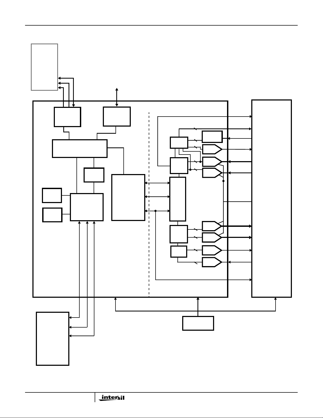
Simplified Block Diagram
HOST
COMPUTER
DAT A
ADDRESS
CONTROL
ISL3873
USB
ON-CHIP
ROM
ON-CHIP
RAM
PC CARD
HOST
INTERFACE
MICRO-
PROGRAMMED
MAC ENGINE
WEP
ENGINE
MEMORY
CONTROLLER
USB
HOST
INTERFACE
INTERFACE
SERIAL
CONTROL
PHY
(MDI)
(MMI)
ISL3873
DATA I/O
AGC
CTL
DEMOD
I/O
MOD
TX
ALC
1
1
7
6
6
6
6
7
6
THRESH.
DETECT
IF
DAC
I ADC
Q ADC
I DAC
Q DAC
TX
DAC
TX
ADC
ANT_SEL
RX_RF_AGC
RX_IF_DET
RX_IF_AGC
RXI±
RXQ±
V
REF
TXI±
TXQ±
TX_IF_AGC
TX_AGC_IN
PRISM RADIO
RF SECTION
ADDRESS
DAT A
SELECT
EXTERNAL
SRAM AND
FLASH
MEMORY
MEDIUM ACCESS
2
CONTROLLER
BASEBAND PROCESSOR
44MHz CLOCK
SOURCE †
†
THE ISL3873 MUST BE SUPPLIED WITH A
SEPARATE CLOCK WHEN USB IS USED.
RADIO AND SYNTH
SERIAL CONTROL

ISL3873
ISL3873 Signal Descriptions
HOST INTERFACE PINS
PIN NAME PIN I/O TYPE DESCRIPTION
HA0-9 5V tol, CMOS, Input, 50K Pull Down Host PC Card Address Input, Bits 0 to 9
HCE1- 5V tol, CMOS, Input, 50K Pull Up Host PC Card Select, Low Byte
HCE2- 5V tol, CMOS, Input, 50K Pull Up Host PC Card Select, High Byte
HD0-15 5V tol, BiDir, 2mA, 50K Pull Down Host PC Card Data Bus, Bit 0 to 15
HINPACK- CMOS Output, 2mA Host PC Card I/O Decode Confirmation
HIORD- 5V tol, CMOS, Input, 50K Pull Up Host PC Card I/O Space Read Strobe
HIOWR- 5V tol, CMOS, Input, 50K Pull Up Host PC Card I/O Space Write Strobe
HRDY/HIREQ- CMOS Output, 4mA Host PC Card interrupt Request (I/O Mode), also used as PC Card
Ready (Memory Mode) output which is asserted to indicate card
initialization is complete
HOE- 5V tol, CMOS, Input, 50K Pull Up Host PC Card Memory Attribute Space Output Enable
HREG- 5V tol, CMOS, Input, 50K Pull Up Host PC Card Attribute Space Select
RESET 5V tol, CMOS, ST Input, 50K Pull Up Hardware Reset. Self-asserted by internal pull-up at power-on. Clock
signal CLKIN or XTALIN must be available before negation of Reset.
Value of MD[15..0] copied to MDIR[15..0] and various control register
bits on the first MCLK following release of Reset
HSTSCHG- CMOS Output, 4mA Host PC Card Status Change
HWAIT- CMOS Output, 4mA Host Wait, asserted to indicate data transfer not complete and to force
force host bus wait states
HWE- 5V tol, CMOS Input, 50K Pull Up Host PC Card Memory Attribute Space Write Enable
USB INTERFACE PINS
PIN NAME PIN I/O TYPE DESCRIPTION
USB+ CMOS BiDir, 2mA, (Also USB Transceiver) USB, MBUS Address Bit 20, or I/O as PL5
USB- CMOS BiDir, 2mA, (Also USB Transceiver) USB, MBUS Address Bit 21, or I/O as PL6
USB_DETECT Input, 5V tolerant, pull-down Sense USB VBUS to indicate cable attachment
MEMORY INTERFACE PINS
PIN NAME PIN I/O TYPE DESCRIPTION
MUBE- / MA0 /
MWEH-
MA1-18 CMOS TS Output, 2mA MBUS Address Bits 1 to 18
PL4-MA19 CMOS BiDir, 2mA MBUS Address Bit 19
MLBE- CMOS TS Output, 2mA, 50K Pull Up MBUS Lower Byte Enable, or I/O as PM2
MOE- CMOS TS Output, 2mA Memory Output Enable
MWE- / MWEL- CMOS TS Output, 2mA Low (or only) Byte Memory Write Enable
RAMCS- CMOS TS Output, 2mA RAM Select
NVCS- CMOS TS Output, 2mA NV Memory Select
MD0-7 5V tol, CMOS, BiDir, 2mA, 100K Pull Up MBUS Low Data Byte, Bits 0 to 7
MD8-15 5V tol, CMOS, BiDir, 2mA
CMOS TS Output, 2mA MBUS Upper Byte Enable for x16 Memory; MBUS Address Bit 0 (byte)
for x8 Memory; High Byte Write Enable for 2 x8 Memories
MBUS High Data Byte, Bits 8 to 15
50K Pull-Downs on MD15, MD14, MD13, MD11,
MD10, MD09
50K Pull-Ups MD12, MD08
Default power up states are defined by pull-up and pull-down internal
resistors as shown. Device defaults to external EEPROM for boot up
mode. Using external 10K resistors, configure these pins according to
Table 4 to change power-up configuration
3

ISL3873
MAC RADIO INTERFACE AND GENERAL PURPOSE PORT PINS
DESCRIPTION OF FUNCTION
PIN NAME PIN I/O TYPE
PJ4 CMOS BiDir, 2mA PE1
PJ5 CMOS BiDir, 2mA, 50K Pull Up LE_IF
PJ6 CMOS BiDir, 2mA LED1
PJ7 CMOS BiDir, 2mA, 50K Pull Up RADIO_PE
PK0 CMOS BiDir, 2mA, ST, 50K Pull Down LE_RF
PK1 CMOS BiDir, 2mA, 50K Pull Down SYNTHCLK
PK2 CMOS BiDir, 2mA, 50K Pull Down SYNTHDATA
PK3 CMOS BiDir, 2mA PA_PE
PK4 CMOS BiDir, 2mA PE2
PK7 CMOS BiDir, 2mA CAL_EN
PL3 CMOS BiDir, 2mA TR_SW_BAR
PL7 CMOS BiDir, 2mA, Pull Down TR_SW
SERIAL EEPROM PORT PINS
PIN NAME PIN I/O TYPE DESCRIPTION
PJ0 CMOS BiDir SCLK, Serial Clock
PJ1 CMOS BiDir, 50K Pull Down SD, Serial Data Out
PJ2 CMOS BiDir, 50K Pull Down MISO, Serial Data IN
TCLKIN (CS_) CMOS BiDir CS_, Chip Select
(IF OTHER THAN I/O PORT)
CLOCKS PORT PINS
PIN NAME PIN I/O TYPE DESCRIPTION
CLKIN CMOS Input, 50K Pull Down External Clock Input to MCLK prescaler (at >= 2X Desired MCLK
Frequency, Typically 44-48MHz)
XTALIN Analog Input 32.768kHz Crystal Input
XTALOUT CMOS Output, 2mA 32.768kHz Crystal Output
CLKOUT CMOS, TS Output, 2mA Internal Clock Output (Selectable as MCLK, TCLK, or TOUT0)
BBP_CLK Input Baseband Processor Clock. The nominal frequency for this clock is
44MHz. This is used internally to generate divide by 2 and 4 for the
transceiver clock
BASEBAND PROCESSOR RECEIVER PORT PINS
PIN NAME PIN I/O TYPE DESCRIPTION
RX_IF_AGC O Analog drive to the IF AGC control
RX_RF_AGC O Drive to the RF AGC stage attenuator. CMOS digital
RX_IF_DET I Analog input to the receive power A/D converter for AGC control
RXI, ± I Analog input to the internal 6-bit A/D of the In-phase received data. Balanced differential 10+/11RXQ, ± I Analog input tothe internal 6-bit A/Dof the Quadraturereceived data. Balanceddifferential 13+/14-
BASEBAND PROCESSOR TRANSMITTER PORT PINS
PIN NAME PIN I/O TYPE DESCRIPTION
TX_AGC_IN I Input to the transmit power A/D converter for transmit AGC control
TX_IF_AGC O Analog drive to the transmit IF power control
TXI ± O TX Spread baseband I digitaloutputdata.Dataisoutput at the chip rate. Balanced differential 23+/24TXQ ± O TX Spread baseband Q digital output data. Data is output at the chip rate. Balanced differential
29+/30-
4

ISL3873
MISC CONTROL PORT PINS
PIN NAME PIN I/O TYPE DESCRIPTION
ANTSEL O The antenna select signal changes state as the receiver switches from antenna to
antenna during the acquisition process in the antenna diversity mode. This is a
complement for ANTSEL (pin 40) for differential drive of antenna switches
ANTSEL O The antenna select signal changes state as the receiver switches from antenna to
antenna during the acquisition process in the antenna diversity mode. This is a
complement for ANTSEL (pin 39) for differential drive of antenna switches
TestMode I/O Factory level test pin. This pin must be pulled low with a 10K resistor.
CompCap1 I Compensation Capacitor
CompCap2 I Compensation Capacitor
CompRes1 I Compensation Resistor
CompRes2 I Compensation Resistor
DBG(0-4) I/O Debug factory test signals. Do not connect
POWER PORT PINS
PIN NAME PIN I/O TYPE DESCRIPTION
V
DDA
V
DD
SUPPLY5V Power 5V Tolerant DC Power Supply
V
SSA
V
sub
GND Ground Digital Ground
VREF Input Voltage Reference for A/D’s and D/A’s
IREF Input CurrentReference for internal ADCand DAC devices. Requires 12K resistor to ground.
ST = Schmitt Trigger (Hysteresis), TS = Three-State. Signals ending with “-” are active low.
Power DC Power Supply 2.7 - 3.6V (Not Hardwired Together on Chip)
Power DC Power Supply 2.7 - 3.6V
Ground Analog Ground
Ground Analog Ground
ISL3873 PIN NUMBER ASSIGNMENTS
PIN NUMBER SIGNAL NAME PIN NUMBER SIGNAL NAME PIN NUMBER SIGNAL NAME PIN NUMBER SIGNAL NAME
A1 NC C7 HD4 F4 MA5 K16 V
DD
A2 MA10 C8 HD6 F13 HD9
A3 MA13 C9 HD14 F14 HD10 L1 MD8
A4 MA16 C10 HD11 F15 HA2 L2 MD7
A5 GND C11 HD7 F16 HA1 L3 MD10
A6 PL4_MA19 C12 HA7 L4 MD9
A7 DBG2 C13 GND G1 MD12 L13 GND
A8 V
DD
A9 HD3 C15 NC G3 V
C14 DBG3 G2 MD14 L14 RX_RF_AGC
DD
L15 ANT_SEL
A10 HCE2 C16 RESET G4 MA2 L16 ANT_SEL
A11 GND G13 GND
A12 HD15 D1 MA3 G14 HSTSCHG M1 MD5
A13 HA9 D2 MA8 G15 HD0 M2 V
A14 V
DD
D3 MA7 G16 BBP_CLK M3 GND
DD
A15 HA6 D4 MA14 M4 MD6
A16 NC D5 MA17 H1 V
DD
M13 V
DDA
D6 DBG0 H2 MLBE M14 COMPCAP1
B1 V
DD
D7 GND H3 MD11 M15 GND
5

ISL3873
ISL3873 PIN NUMBER ASSIGNMENTS (CONTINUED)
PIN NUMBER SIGNAL NAME PIN NUMBER SIGNAL NAME PIN NUMBER SIGNAL NAME PIN NUMBER SIGNAL NAME
B2 NC D8 HD5 H4 MD13 M16 V
B3 MA9 D9 HIREQ H13 HD2
B4 MA12 D10 HIOWR H14 HD1 N1 MD4
B5 V
DD
D11 HOE H15 HA0 N2 MD0
B6 MA18 D12 NC H16 HD8 N3 MD3
B7 DBG1 D13 HA5 N4 MD2
B8 HD12 D14 HWAIT J1 XTALIN N5 NC
B9 HCE1 D15 SUPPLY5V J2 XTALOUT N6 PJ7
B10 V
DD
D16 HREG J3 RAMCS N7 PK2
B11 HIORD J4 NVCS N8 VDDA
B12 HA8 E1 GND J13 USB_DET N9 V
B13 HWE E2 MA4 J14 V
DD
N10 V
B14 HA4 E3 GND J15 USB- N11 V
B15 NC E4 NC J16 USB+ N12 IREF
B16 DBG4 E13 HA3 N13 V
E14 V
DD
K1 CLKIN N14 NC
C1 MA6 E15 HINPACK K2 MOE N15 RX_IF_AGC
C2 NC E16 GND K3 MWEL N16 TX_IF_AGC
C3 MA11 K4 GND
C4 MA15 F1 MD15 K13 TESTMODE
C5 CLKOUT F2 MA1 K14 GND
C6 HD13 F3 MWEH_MA0 K15 GND
P1 MD1 R1 PJ1
(SDATA)
P2 PJ2
R2 NC T2 V
T1 PJ0
(SCLK)
DD
(MISO)
P3 TCLKIN R3 NC T3 PJ6
(LED1)
P4 PJ5
(LE_IF)
P5 GND R5 PK0
P6 PL7
(TR_SW)
P7 PK7
R4 PJ4
(PE1)
T4 PK1
(SYNTHCLK)
T5 PK4
(LE_RF)
R6 PK3
(PA_PE)
T6 PL3
(PE2)
(TR_SW_BAR)
R7 RXI+ T7 RXI-
(CAL_EN)
P8 V
DDA
R8 V
DDA
T8 V
DDA
P9 GND R9 RXQ+ T9 RXQP10 V
SUB
P11 VREF R11 V
P12 V
DDA
P13 COMPRES2 R13 COMCAP2 T13 V
R10 RX_IF_DET T10 TX_AGC_IN
DDA
T11 V
SSA
R12 TXI+ T12 TXI-
SSA
P14 N C R14 TXQ+ T14 TXQP15 NC R15 NC T15 COMPRES1
P16 NC R16 NC T16 NC
DD
(RADIO_PE)
(SYNTHDATA)
SSA
SUB
DD
SSA
6

ISL3873
Absolute Maximum Ratings Thermal Information
Supply Voltage, VCC . . . . . . . . . . . . . . . . . . . . . . . . . . . . . . . . . 3.6V
Input, Output or I/O Voltage. . . . . . . . . . . .GND -0.5V to VCC+0.5V
ESD Classification . . . . . . . . . . . . . . . . . . . . . . . . . . . . . . . . .Class 2
Operating Conditions
Voltage. . . . . . . . . . . . . . . . . . . . . . . . . . . . . . . . . . . . . . . . . . . +3.3V
Ambient Temperature Range. . . . . . . . . . . . . . . . . . . -40oC to 85oC
CAUTION: Stresses above those listed in “Absolute Maximum Ratings” may cause permanent damage to the device. This is a stress only rating and operation of the
device at these or any other conditions above those indicated in the operational sections of this specification is not implied.
NOTE:
1. θJA is measured with the component mounted on an evaluation PC board in free air.
DC Electrical Specifications
PARAMETER SYMBOL TEST CONDITIONS MIN TYP MAX UNITS
Power Supply Current I
CCOP
Input Leakage Current I
Output Leakage Current I
O
Logical One Input Voltage V
Logical Zero Input Voltage V
Logical One Output Voltage V
Logical Zero Output Voltage V
OH
OL
Input Capacitance C
Output Capacitance C
OUT
NOTE: All values in this table have not been measured and are only estimates of the performance at this time.
VCC = 3.6V, CLK Frequency 44MHz - - 175 mA
VCC = Max, Input = 0V or V
I
VCC = Max, Input = 0V or V
VCC = Max, Min 0.7V
IH
VCC = Min, Max - - 0.3V V
IL
IOH = -1mA, VCC = Min 0.9V
IOL = 2mA, VCC = Min - 0.1 0.1V
CLK Frequency 1MHz. All measurements
IN
referenced to GND. TA = 25oC
CLK Frequency 1MHz. All measurements
referenced to GND. TA = 25oC
Thermal Resistance (Typical, Note 1) θJA (oC/W)
BGA Package. . . . . . . . . . . . . . . . . . . . . . . . . . . . . . 55
Maximum Storage Temperature Range. . . . . . . . . . -65oC to 150oC
Maximum Junction Temperature . . . . . . . . . . . . . . . . . . . . . . .100oC
Maximum Lead Temperature (Soldering 10s) . . . . . . . . . . . . .300oC
(Lead Tips Only)
CC
CC
-10 1 10 mA
-10 1 10 mA
CC
CC
--V
--V
CC
V
- 5 10 pF
- 5 10 pF
AC Electrical Specifications
PARAMETER SYMBOL MIN TYP MAX UNITS
CLOCK SIGNAL TIMING
OSC Clock Period (Typ. 44MHz) t
High Period t
Low Period t
EXTERNAL MEMORY READ INTERFACE
MOE-Setup Time from RAMCS_ t
MOE_Setup Time from MA (17..0) t
MA (17..1) Hold Time from MOE_ Rising Edge t
RAMCS_ Hold from MOE_ Rising Edge t
MD (15..0) Enable from MOE_ Falling t
MO (15..0) Disable from MOE_ Rising Edge t
EXTERNAL MEMORY WRITE INTERFACE
MA (17..0) Setup to MWE_ Falling Edge t
RAMCS_ Setup to MWE t
MA (17..0) Hold from MWE_ Rising Edge t
RAMCS _ Hold from MWE_ Rising Edge t
MD (15..0) Setup to MWE_ Rising Edge t
MD (15..0) Hold from MWE_ Rising Edge t
SYNTHESIZER
SYNTHCLK(PK1) Period t
CYC
H1
L1
S1
S2
H1
H2
E1
D1
S3
S4
H3
H4
S5
H5
CYC
20 20.8 200 ns
10 10.4 - 10 10.4 - -
0--ns
0
-
-ns
20 - - ns
20 - - ns
5
-
-
-
-ns
100 ns
000ns
0--ns
15 - - ns
15 - - ns
40 - - ns
15 - - ns
83 - 4,000 ns
7

ISL3873
AC Electrical Specifications (Continued)
PARAMETER SYMBOL MIN TYP MAX UNITS
SYNTHCLK(PK1) Width Hi t
SYNTHCLK(PK1) Width Lo t
H1
L1
SERIAL PORT
SYNTHCLK(PK1) Clock Period t
CYC
Low Width tH1, t
Delay from Clock Falling Edge to SPCSx, SPAS, SPREAD,
t
CD
SYNTHDATA(PK2) Outputs
Setup Time of SYTHNDATA(PK2) Read to SYTHNCLK(PK1) Falling Edge t
Hold Time ofSYTHNDATA(PK2) Read from SYTHNCLK(PK1) Falling Edge t
Hold Time of SYTHNDATA(PK2) Write from SYTHNCLK(PK1) Falling Edge t
DRS
DRH
DWH
SYSTEM INTERFACE - PC CARD IO READ 16
Data Delay After HIORD- t
Data Hold Following HIORD- t
HIORD- Width Time t
Address Setup Before HIORD- t
Address Hold Following HIORD- t
HCE(1,2)- Setup Before HIORD- t
HCE(1,2)- Hold After HIORD- t
HREG- Setup Before HIORD- t
HREG- Hold Following HIORD- t
HINPACK- Delay Falling from HIORD- t
HINPACK- Delay Rising from HIORDN d
HWAIT- t
Data Delay from HWAIT- Rising t
HWAIT- Width Time t
DIORD
HIORD
WIORD
SUA
HA
SUCE
HCE
SUREG
HREG
DFINPACK
DRINPACK
DFWT
DRWT
WWT
SYSTEM INTERFACE - PC CARD IO WRITE 16
Data Setup Before HIOWR- t
Data Hold Following HIOWR- t
HIOWRN- Width Time t
Address Setup Before HIOWR- t
Address Hold Following HIOWR- t
HCE(1,2)- Setup Before HIOWR- t
HCE(1,2)- Hold Following HIOWR- t
HREG- Setup Before HIOWR- t
HREG- Hold Following HIOWR- t
HWAIT- Delay Falling from HIOWR- t
HWAIT- Width Time t
HIOWRN High from HWAIT- High t
SUIOWR
HIOWR
WIOWR
SUA
HA
SUCE
HCE
SUREG
HREG
DFWT
WWT
DRIOWR
BASEBAND SIGNALS
Full Scale Input Voltage (V
) 0.25 0.50 1.0 V
P-P
Input Bandwidth (-0.5dB) - 20 - MHz
Input Capacitance -5-pF
Input Impedance (DC) 5--kΩ
FS (Sampling Frequency) - - 22 MHz
L1
t
/2 - 10 - t
CYC
t
/2 - 10 - t
CYC
/2 + 10 ns
CYC
/2 + 10 ns
CYC
83ns - 4000 ns
t
/2 -10 - t
CYC
/2 + 10 ns
CYC
-10-ns
15 - - ns
0--
0--
- - 100 ns
0--ns
165 - - ns
70 - - ns
20 - - ns
5--ns
20 - - ns
5--ns
0--ns
0 - 45 ns
30 - 45 ns
- - 35 ns
--0ns
- - 12,000 ns
30 - 92 ns
20 - - ns
165 - - ns
70 - - ns
20 - - ns
5--ns
20 - - ns
5--ns
0--ns
- - 35 ns
- - 12,000 ns
0--ns
8

Waveforms
ADDRESS
MA(17..1)
RAMCS_
MOE_
MD(15..0)
ISL3873
t
H1
t
t
S1
t
S2
t
E1
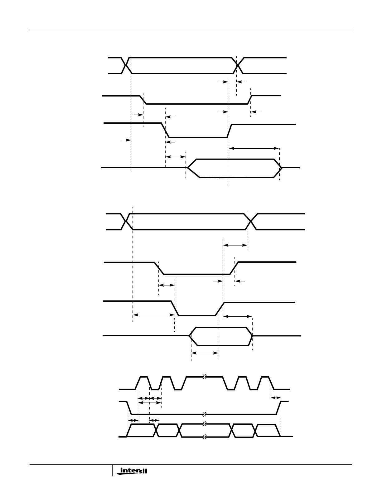
FIGURE 1. EXTERNAL MEMORY READ TIMING
H2
t
D1
ADDRESS
MA(17..1)
RAMCS_
MWE_
MD(15..0)
SYNTHCLK
t
H3
t
S4
t
S3
t
S5
t
H4
t
H5
FIGURE 2. EXTERNAL MEMORY WRITE TIMING
t
H1tL1
t
D3
SYNLE
SPCSPWR
SYNTHDATA
9
t
CYC
t
D1
D[n] D[n -1] D[n -2] D[2] D[1] D[0]
t
D2
FIGURE 3. SYNTHESIZER

Waveforms (Continued)
HA[15:0]
HREG-
t
SUREG
ISL3873
t
HREG
HCE(1, 2) -
HIORD-
HINPACK-
HWAIT-
HD[15:0]
HA[15:0]
t
SUA
I
SUCE
t
WIORD
t
DIORD
t
DFINPACK
t
DFWT
t
WWT
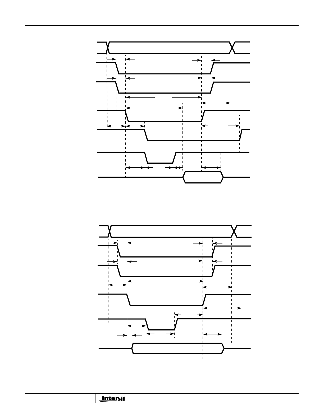
FIGURE 4. PC CARD IO READ 16
t
HCE
t
DRWT
t
DRINPACK
t
HIORD
t
HA
HREGN-
HCE (1, 2) -
HIOWR-
HWAIT-
HD[15:0]
t
SUIOWR
t
SUREG
t
SUCE
t
SUA
t
DFWT
t
WWT
t
WIOWR
FIGURE 5. PC CARD IO WRITE 16
t
HREG
t
HCE
t
DRIOWR
t
DRINPACK
t
HIOWR
t
HA
10
 Loading...