Beko Samsung V3 Service Manual

Beko Elektronik A.S Service Manual Plasma Display Module-Samsung V3
DATE: July 15, 2004
Beko
SERVICE MANUAL
107cm (42 Inch) Wide Plasma Display Module
MODEL : 42” S3.1 PDP
1 / 44

Beko Elektronik A.S Service Manual Plasma Display Module-Samsung V3
CONTENTS
1.Overview
1-1 Model Name of plasma Display
1-2 External View
1-3 Specifications
2. Precaution
2-1 Handling Precaution for Plasna Display,
2-2 Safety Precautions for Service (Handling, prevention of a electrical shock, measure against
power outage, etc)
3. Name & Function
3-1 Layout of Assemblies
3-2 Block Diagram:
3-3 Main function of Each Assembly
3-4 Product/Serial Label Location
4. Operation checking after rectification
4-1 Flow chart
4-2 Defects , Symptoms and Detective Parts
5. Disassembling / Assembling
5-1 Tools and measurement equipment
5-2 Exploded View
5-3 Disassembling & Re-assembling
6. Operation Check after Repair Service
6-1 Check Item
6-2 Check Procedure
7. Operation Check
7-1 Adjustment Specification, Checking Position etc.
7-2 Adjusting procedure
8. Spare part list for the panel
2 / 44
Beko Elektronik A.S Service Manual Plasma Display Module-Samsung V3
1. Overview
1-1 Model Name of Plasma Display
MODEL : 42” S3.1 PDP (S42SD-YD05)
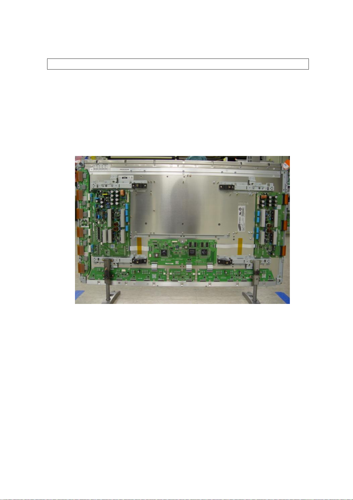
1-2 External View
【 M1 = X Board + Y Board + Logic Board 】
3 / 44

Beko Elektronik A.S Service Manual Plasma Display Module-Samsung V3
1-3 Specifications
No
Item Specification
1 Pixel 852 (H) × 480 (V) pixels (1 pixel = 1 R,G,B cells)
2 Number of Cells 2556 (H) × 480 (V)
3 Pixel Pitch 1.095 (H) ㎜ × 1.110 (V) ㎜
R 0.365 (H) ㎜ × 1.110 (V) ㎜
4
Cell Pitch
G 0.365 (H) ㎜ × 1.110 (V) ㎜
B 0.365 (H) ㎜ × 1.110 (V) ㎜
5 Display size
932.940 (H) ㎜ × 532.800(V) ㎜
[ 36.73 inch × 20.98 inch ]
6 Screen size Diagonal 42" Color Plasma Display Module
7 Screen aspect 16 : 9
8 Display color 16.77 million colors
Over 160°
9 Viewing angle
(Angle with 50% and greater brightness perpendicular to PDP
module)
10
11
12
13
14
Dimensions 982 (W) × 582 (H) × 52.9 (D) ㎜
Weight Module 1 About 16.6 kg
Packing weight Module 1
Packing size L 1175 * W 1140 * H 970 (mm) / 10pcs/BOX
Broadcasting reception
PL42SD003C 60Hz/ 50Hz, LVDS
Vertical frequency
and
Video/Logic Interface
4 / 44
240kg ± 5kg (including modules) /
10pcs/BOX

Beko Elektronik A.S Service Manual Plasma Display Module-Samsung V3
2. PRECAUTIONS
** To prevent the risks of unit damage, electrical shock and radiation, take the
following safety, service, and ESD precautions.
2-1 Handling Precautions for Plasma Display
n PDP module use high voltage that is
dangerous to human. Before operating
PDP, always check the dust to prevent
circuit short. Be careful touching the
circuit device when power is on.
n PDP module is sensitive to dust and
humidity. Therefore, assembling and
disassembling must be done in no dust
place.
n PDP module has a lot of electric
devices. Service engineer must wear
equipment(for example , earth ring) to
prevent electric shock and working
n PDP module use a fine pitch connector
which is only working by exactly
connecting with flat cable. Operator
must pay attention to a complete
connection when connector is
reconnected after repairing.
n The capacitor’s remaining voltage in
the PDP module’s circuit board
temporarily remains after power is off.
Operator must wait for discharging of
remaining voltage during at least 1
minute.
clothes to prevent electrostatic.
2-2 Safety Precautions for Service (Handling, prevention of a electrical shock, measure
against power outage, etc)
5 / 44

Beko Elektronik A.S Service Manual Plasma Display Module-Samsung V3
( Safety Precautions )
n Before replacing a board, discharge forcibly
The remaining electricity from board.
n When connecting FFC and TCPs to the
module, recheck that they are perfectly
connected.
n To prevent electrical shock, be careful not
to touch leads during circuit operations.
n To prevent the Logic circuit from being
damaged due to wrong working, do not
connect/disconnect signal cables during
circuit operations.
n Do thoroughly adjustment of a voltage label
and voltage-insulation.
n Before reinstalling the chassis and the
n If any parts of wire is overheats of damaged,
replace it with a new specified one
immediately, and identify the cause of the
problem and remove the possible
dangerous factors.
n Examine carefully the cable status if it is
twisted or damaged or displaced. Do not
change the space between parts and circuit
board. Check the cord of AC power
preparing damage.
n Product Safety Mark : Some of electric or
implement material have special
characteristics invisible that was related on
safety. In case of the parts are changed
with new one, even though the Voltage and
chassis assembly, be sure to use all
protective stuffs including a nonmetal
controlling handle and the covering of
partitioning type.
n Caution for design change : Do not install
any additional devices to the module, and
do not change the electrical circuit design.
n For example: Do not insert a subsidiary
audio or video connector. If you insert It, It
cause danger on safety. And, If you change
the design or insert, Manufactor guarantee
will be not effect. .
Watt is higher than before, the Safety and
Protection function will be lost.
n The AC power always should be turned off,
before next repair..
n Check assembly condition of screw, parts
and wire arrangement after repairing.
Check whether the material around the
parts get damaged.
6 / 44

Beko Elektronik A.S Service Manual Plasma Display Module-Samsung V3
( Precaution when repairing ESD )
n There is ESD which is easily damaged by
electrostatics.(for example Integrated circuit,
FET ) Electrostatic damage rate of product
will be reduced by the following technics
n Before handling semiconductor
parts/assembly, must remove positive
electric by ground connection, or must wear
the antistatic wrist-belt and ring. ( It must be
operated after removing dust on it – It
comes under precaution of electric shock.)
n After removing ESD assembly, put on it with
aluminum stuff on the conductive surface to
prevent charging.
n Do not use chemical stuff using Freon. It
n Must use anti-static solder removal device.
Most removal device do not have antistatic
which can charge a enough positive electric
enough damaging ESD.
n Before removeing the protective material
from the lead of a new ESD, bring the
protective material into contact with the
chassis or assembly that the ESD is to be
installed on.
n When handing an unpacked ESD for
replacement, do not move around too much.
Moving (legs on the carpet, for example)
generates enough electrostatic to damage
the ESD.
generates positive electric that can damage
ESD.
n Must use a soldering device for ground-tip
when soldering or de-soldering ESD.
n Do not take a new ESD from the protective
case until the ESD is ready to be installed.
Most ESD have a lead, which is easily
short-circuited by conductive materials
(such as conductive foam and aluminum)
7 / 44
Beko Elektronik A.S Service Manual Plasma Display Module-Samsung V3
3.NAME & FUNCTION
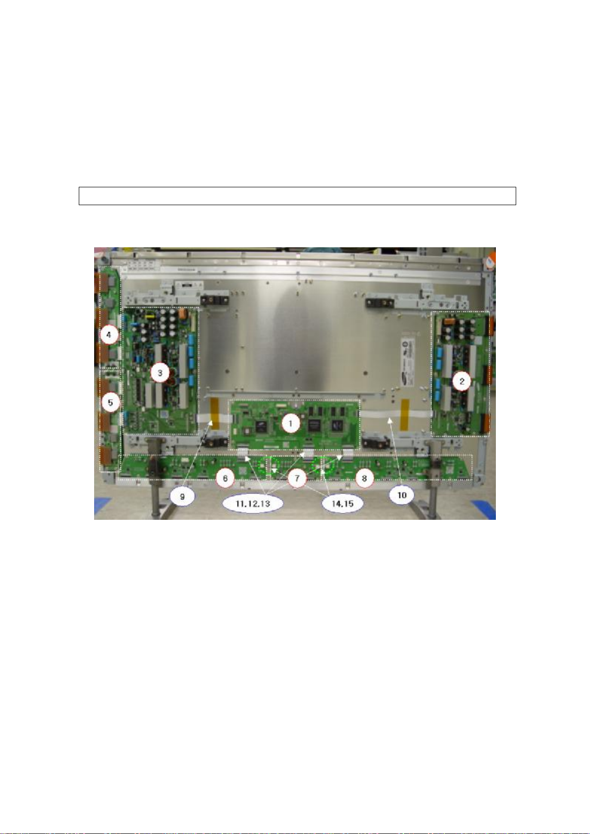
3-1 Layout of Assemblies
8 / 44
Beko Elektronik A.S Service Manual Plasma Display Module-Samsung V3
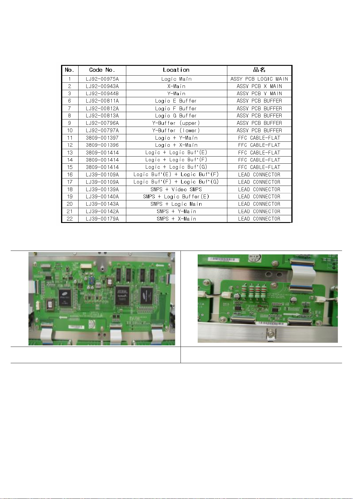
1. L-Main 7. F-Buffer
9 / 44
Beko Elektronik A.S Service Manual Plasma Display Module-Samsung V3
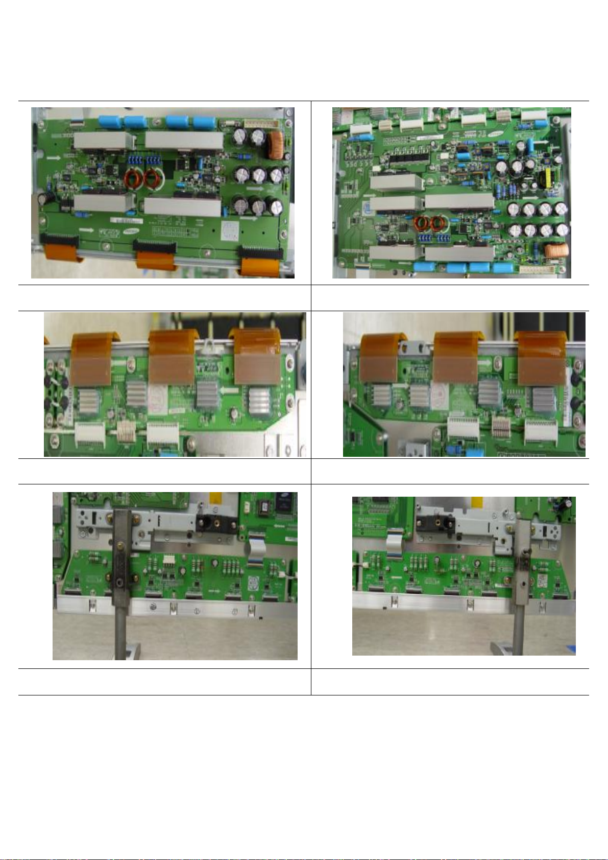
2. X-Main 3. Y-Main
4, Y-Buffer (upper) 5. Y-Buffer (lower)
6. E-Buffer 8. G-Buffer
10 / 44
Beko Elektronik A.S Service Manual Plasma Display Module-Samsung V3
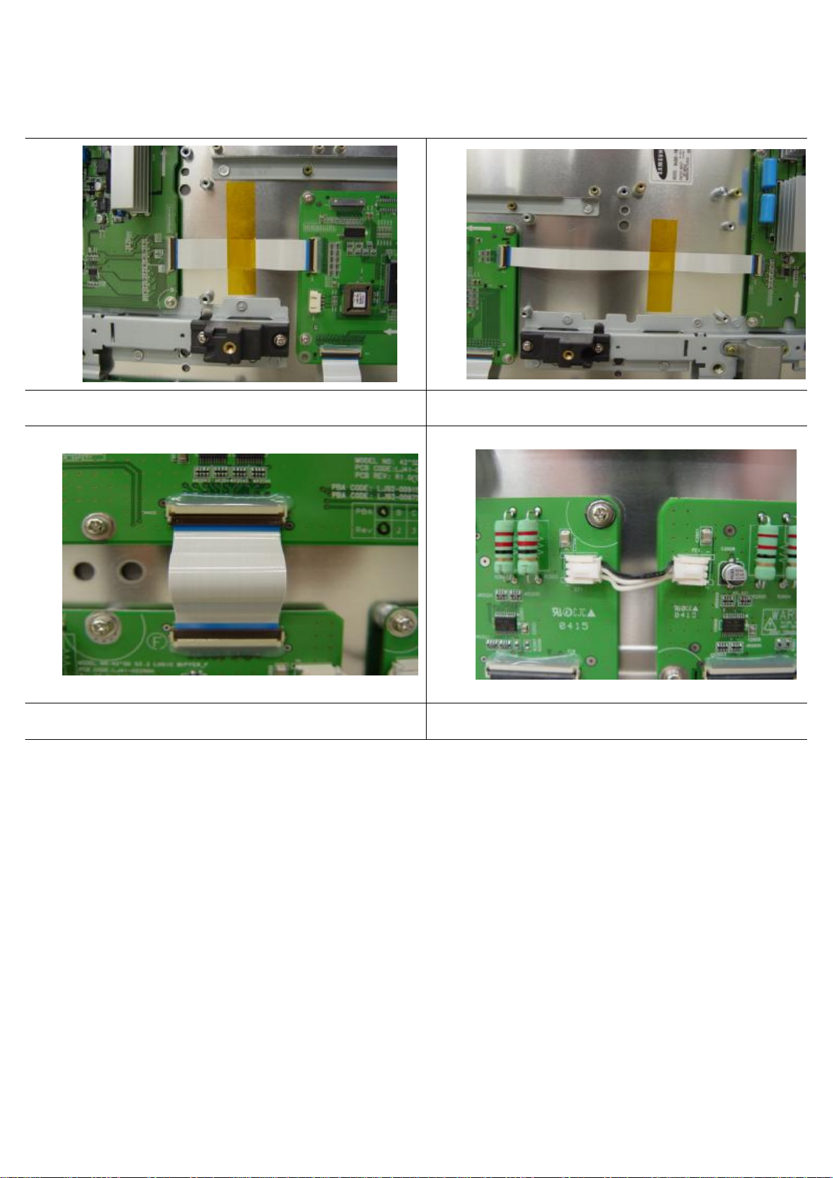
9. Logic + Y-Main 10. Logic + X-Main
11. 12. 13. Logic + Logic Buf’(E,F,G) 14. 15. Logic Buffer 間
3-2 BLOCK DIAGRAM
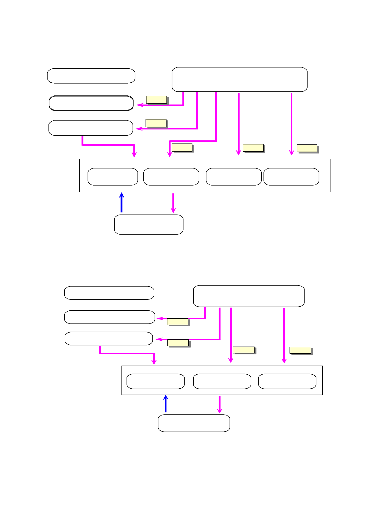
3-2-1 BLOCK DIAGRAM FOR DRIVE CIRCUIT OPERATION
11 / 44
Beko Elektronik A.S Service Manual Plasma Display Module-Samsung V3
Logic 신호입력부
SignalinputSection
Ysc,SIA,SIB,CLK,LESTB
(
(Ysc,SIA,SIB,CLK,LE,STB)
(5Vd,17Vcc,75Vsc,165Vs,220Vset)
PowerSupplyInput
Logic 신호 Buffer)
Logicsignalbuffer
FetGateDriver)
Recovery
Switching
5V
17V
165V
Main
Switching
Recoverycircuit
(RecoveryCap)
< DRIVE Y Board >
220V
Vset
Switching
Vscan
Switching
75V
Logic 신호입력부
Signalinputsection
(Xr,Xf,Xs,Xg)
(Xr,Xf,Xs,Xg)
Logic 신호 Buffer)
Logicsignalbuffer
FetGateDriver)
Recovery
Switching
5V
17V
Recoverycircuit
(RecoveryCap)
< DRIVE X Board >
Powersupplyinput
(5Vd,17Vcc,195Ve,165Vs)
165V
Main
Switching
Switching
195V
Ve
12 / 44
Beko Elektronik A.S Service Manual Plasma Display Module-Samsung V3
Vs
12
Vsc_h
Vset
12
Vs
Yr
Panel
Vset
Ysc_h
Ysc_l
Ysc
10us
Vsc
R5124
1k
Yfr
R5117R5118
RAMP
Ypn
RAMP
Yset
Ypp
RAMP
YDCL
Ys
YgYer
GND
1 2
GND
Vs
YDCH
bead
bead
12
12
YDr
12
YDf
Yf
GND
GND
Vsc_h
Vfr=Vsc_l+12V
30us
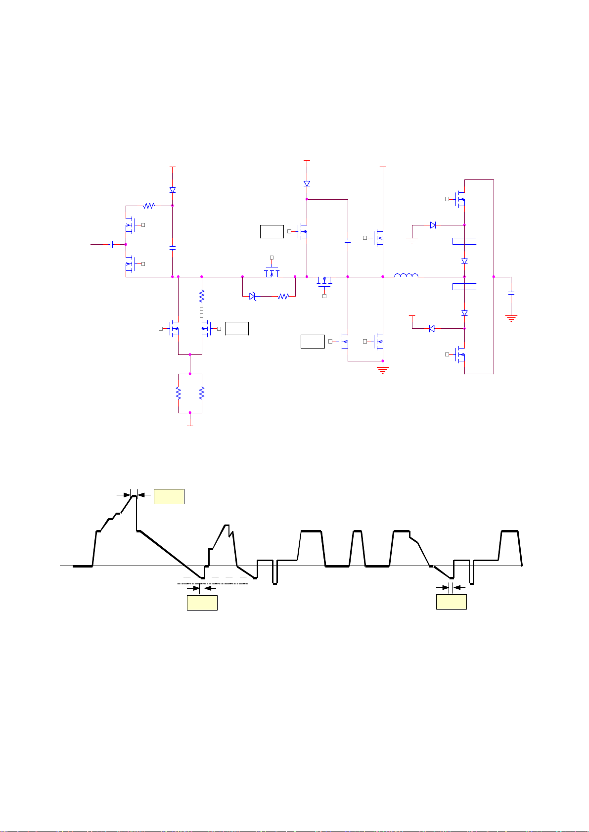
< Drive waveforms >
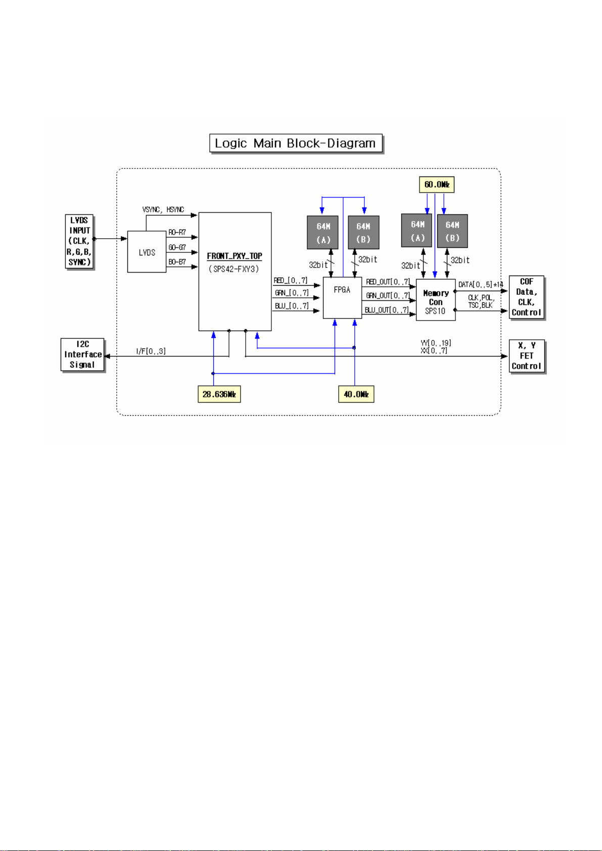
3-2-2 Block Diagram for Logic circuit
13 / 44
Vsc_l
Vs
30us
Beko Elektronik A.S Service Manual Plasma Display Module-Samsung V3
3-3 Main function of Each Assembly
■ X-main board : The X-main board generate a drive signal by switching the FET in synchronization with logic
main board timing and supplies the X electrode of the panel with the drive signal through the
connector.
1) Maintain voltage waveforms (including ERC)
2) Generate X rising ramp signal
3) Maintain Ve bias between Scan intervals
■.Y-main board : The Y-main board generate a drive signal by switching the FET in synchronization with the logic
Main Board timing and sequentially supplies the Y electrode of the panel with the drive signal
through the scan driver IC on the Y-buffer board. This board connected to the panel’s
Y terminal has the following main functions.
1) Maintain voltage waveforms (including ERC)
2) Generate Y-rising Falling Ramp
3) Maintain V scan bias
■ Logic main board : The logic main board generates and outputs the address drive output signal and the X ,Y
drive signal by processing the video signals. This Board buffers the address dirve output
14 / 44
 Loading...