

Page 1
Design Guide
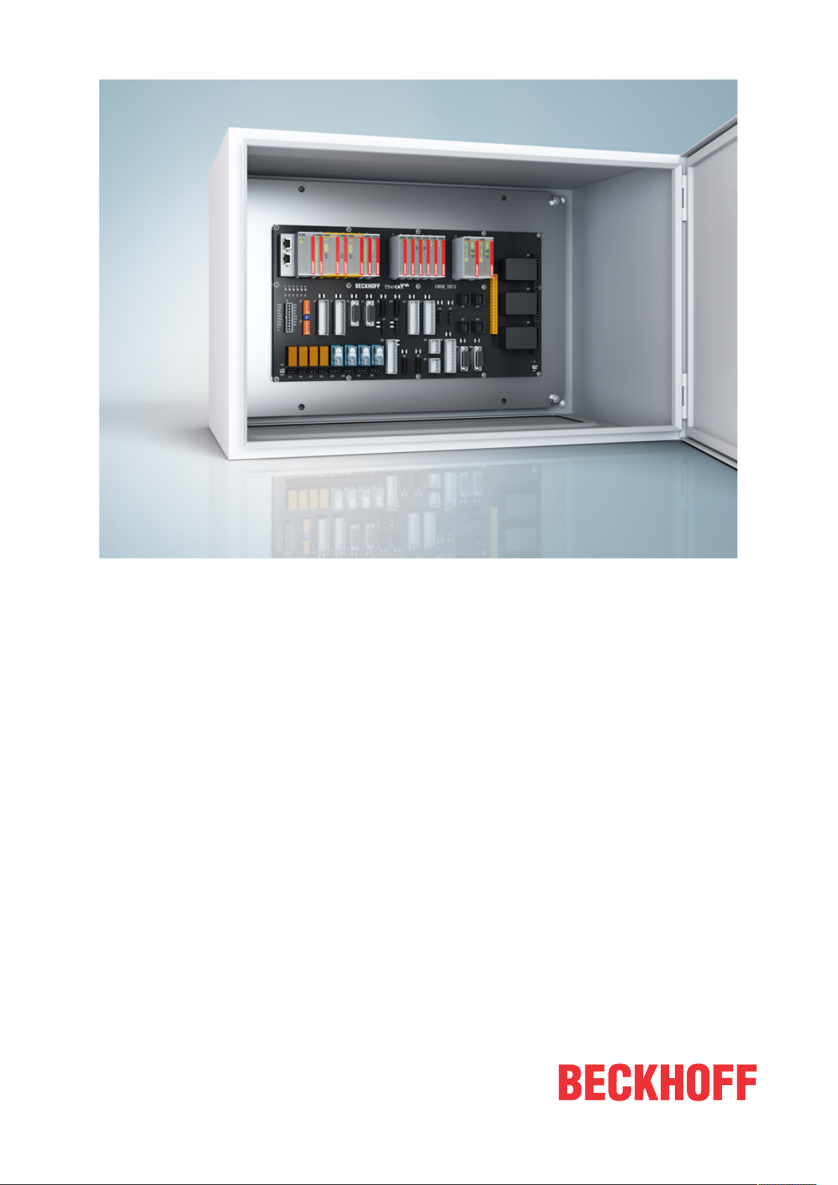
EJ8xxx
Signal-Distribution-Board for standard EtherCAT plug-in
modules
Version:
Date:
6.1
2019-11-22
Page 2

Page 3

Table of contents
Table of contents
1 Foreword ....................................................................................................................................................5
1.1 Notes on the documentation..............................................................................................................5
1.2 Safety instructions .............................................................................................................................6
1.3 Documentation issue status ..............................................................................................................7
1.4 Purpose and area of application........................................................................................................7
2 Technical data - Signal distribution board..............................................................................................8
3 Backplane mounting guidelines...............................................................................................................9
3.1 Minimum distances for ensuring installability ....................................................................................9
3.2 Installation positions ........................................................................................................................10
4 Module placement ...................................................................................................................................11
5 PCB - distances and footprint ................................................................................................................13
6 Structure of the PCB layers....................................................................................................................14
7 Design of power supply ..........................................................................................................................19
8 Physical Communication Layer .............................................................................................................21
9 Routing guildelines .................................................................................................................................22
9.1 EMC guidelines ...............................................................................................................................23
9.2 Impedance and Routing ..................................................................................................................23
10 Appendix ..................................................................................................................................................24
10.1 Support and Service ........................................................................................................................24
EJ8xxx 3Version: 6.1
Page 4

Table of contents
EJ8xxx4 Version: 6.1
Page 5

Foreword
1 Foreword
1.1 Notes on the documentation
Intended audience
This description is only intended for the use of trained specialists in control and automation engineering who
are familiar with the applicable national standards.
It is essential that the documentation and the following notes and explanations are followed when installing
and commissioning these components.
It is the duty of the technical personnel to use the documentation published at the respective time of each
installation and commissioning.
The responsible staff must ensure that the application or use of the products described satisfy all the
requirements for safety, including all the relevant laws, regulations, guidelines and standards.
Disclaimer
The documentation has been prepared with care. The products described are, however, constantly under
development.
We reserve the right to revise and change the documentation at any time and without prior announcement.
No claims for the modification of products that have already been supplied may be made on the basis of the
data, diagrams and descriptions in this documentation.
Trademarks
Beckhoff®, TwinCAT®, EtherCAT®, EtherCATG®, EtherCATG10®, EtherCATP®, SafetyoverEtherCAT®,
TwinSAFE®, XFC®, XTS® and XPlanar® are registered trademarks of and licensed by Beckhoff Automation
GmbH. Other designations used in this publication may be trademarks whose use by third parties for their
own purposes could violate the rights of the owners.
Patent Pending
The EtherCAT Technology is covered, including but not limited to the following patent applications and
patents: EP1590927, EP1789857, EP1456722, EP2137893, DE102015105702 with corresponding
applications or registrations in various other countries.
EtherCAT® is registered trademark and patented technology, licensed by Beckhoff Automation GmbH,
Germany.
Copyright
© Beckhoff Automation GmbH & Co. KG, Germany.
The reproduction, distribution and utilization of this document as well as the communication of its contents to
others without express authorization are prohibited.
Offenders will be held liable for the payment of damages. All rights reserved in the event of the grant of a
patent, utility model or design.
EJ8xxx 5Version: 6.1
Page 6
Foreword
1.2 Safety instructions
Safety regulations
Please note the following safety instructions and explanations!
Product-specific safety instructions can be found on following pages or in the areas mounting, wiring,
commissioning etc.
Exclusion of liability
All the components are supplied in particular hardware and software configurations appropriate for the
application. Modifications to hardware or software configurations other than those described in the
documentation are not permitted, and nullify the liability of Beckhoff Automation GmbH & Co. KG.
Personnel qualification
This description is only intended for trained specialists in control, automation and drive engineering who are
familiar with the applicable national standards.
Description of instructions
In this documentation the following instructions are used.
These instructions must be read carefully and followed without fail!
DANGER
Serious risk of injury!
Failure to follow this safety instruction directly endangers the life and health of persons.
WARNING
Risk of injury!
Failure to follow this safety instruction endangers the life and health of persons.
CAUTION
Personal injuries!
Failure to follow this safety instruction can lead to injuries to persons.
NOTE
Damage to environment/equipment or data loss
Failure to follow this instruction can lead to environmental damage, equipment damage or data loss.
Tip or pointer
This symbol indicates information that contributes to better understanding.
EJ8xxx6 Version: 6.1
Page 7

Foreword
1.3 Documentation issue status
Version Comment
6.1 • Update chapter Structure of the PCB layers
6.0 • Migration
• Update structure
1.4 Purpose and area of application
This document is meant for developers who would like to create a backplane or an EJ distribution board
upon which standard EtherCAT plug-in modules should be used.
This document gives information about the general design of an EJ distribution board for standard EtherCAT
plug-in modules.
When secure EJ modules should be used along with standard EtherCAT plug-in modules please note the
additional requirements and notes of the supplementary Design Guide EJ-Backplane for TwinSAFE-modules.
EJ8xxx 7Version: 6.1
Page 8
Technical data - Signal distribution board
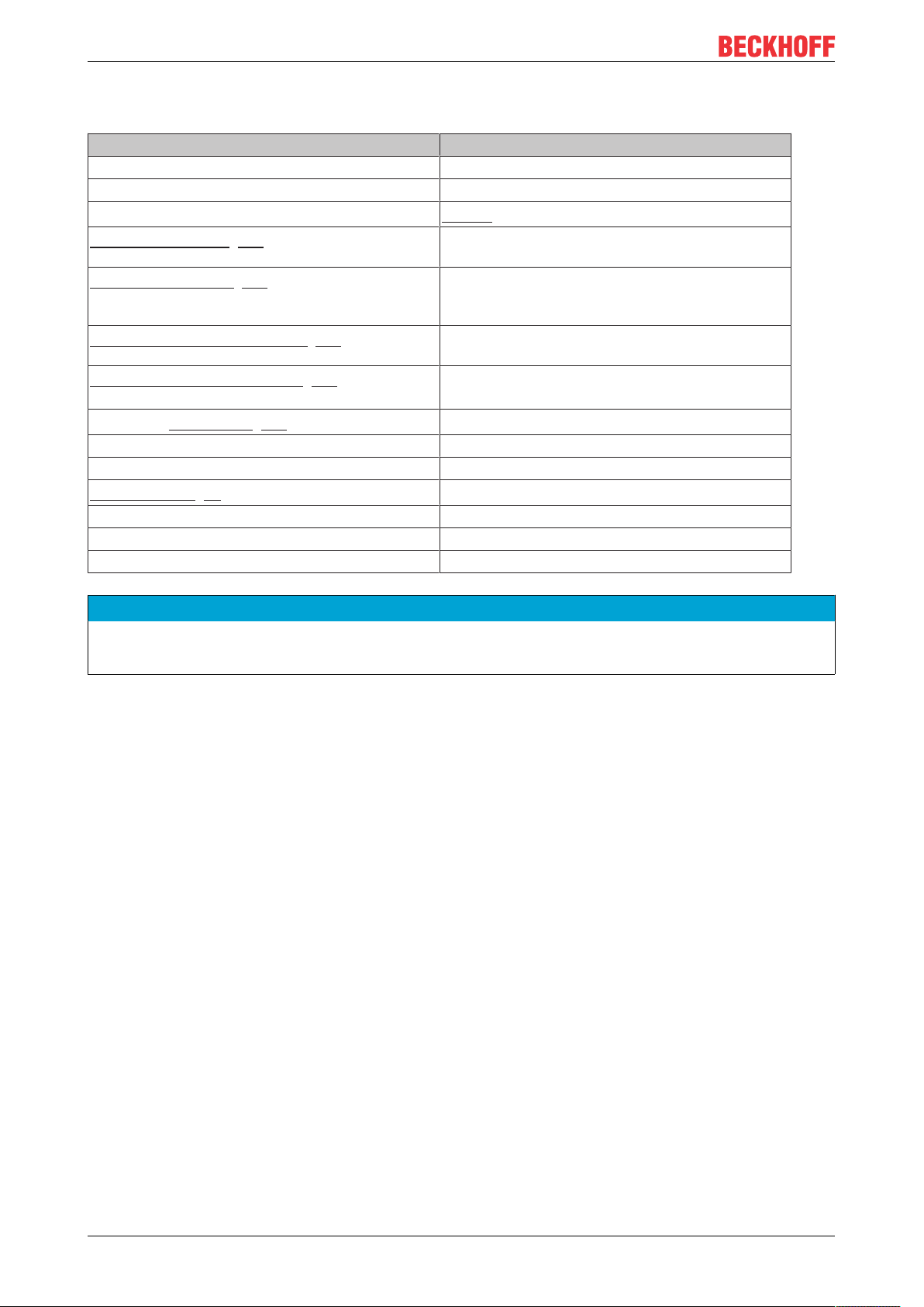
2 Technical data - Signal distribution board
Technical data Signal distribution board
PCB layer stack Multilayer PCB, min. 4 layers
PCB thickness 1.6mm ± 10%
Board connector
Placing of modules [}11]
E-bus power supply [}19]
Refresh of E-bus power supply [}20]
Air gap and leakage distances [}12] between E-
bus- and field signals
Differential impedance [}23] of the LVDS traces
SGND connection via mounting bolts
Mounting hole distances max. 100mm
Reaching area [}9]
Module depth above PCB min. 55mm
Distance between PCB and mounting surface min. 4mm
Mounting position Standard
Samtec: SSQ-120-01-L-D
Starting from the left:
Coupler, power supply module, EJ-modules
EJ1100 (2.2A)
EJ1101-0022 + (EJ9400 (2.5A) or EJ9404 (12A))
CX + EK1110-0043
EJ9400 (2.5A)
EJ9404 (12A)
typ. 1.2mm
100Ω
92mm
NOTE
Damage to devices possible
Note the specifications and notes for the components used!
EJ8xxx8 Version: 6.1
Page 9

Backplane mounting guidelines
3 Backplane mounting guidelines
In order to avoid physical stress on the backplane in the module installation process, the backplane pcb
should be mounted in the switch cabinet as described in the following figure.
Fig.1: Maximum distances between mounting holes and PCB
3.1 Minimum distances for ensuring installability
Note the dimensions shown in the following diagram for the design of the signal distribution board to ensure
safe latching and simple assembly / disassembly of the modules.
Fig.2: Mounting distances EJ module - PCB
Observing the reaching area
A minimum reaching area of 92mm is required for assembly / disassembly, in order to be able to
reach the mounting tabs with the fingers.
Adherence to the recommended minimum distances for ventilation (see section Installation position
[}10]) ensures an adequate reaching area.
The signal distribution board must have a thickness of 1.6mm and a minimum distance of 4mm from the
mounting surface, in order to ensure latching of the modules on the board.
EJ8xxx 9Version: 6.1
Page 10

Backplane mounting guidelines
3.2 Installation positions
NOTE
Constraints regarding installation position and operating temperature range
Please refer to the technical data for the installed components to ascertain whether any restrictions regarding the mounting position and/or the operating temperature range have been specified. During installation
of modules with increased thermal dissipation, ensure adequate distance above and below the modules to
other components in order to ensure adequate ventilation of the modules during operation!
The standard installation position is recommended. If a different installation position is used, check whether
additional ventilation measures are required.
Ensure that the specified conditions (see Technical data) are adhered to!
Optimum installation position (standard)
For the optimum installation position the signal distribution board is installed horizontally, and the fronts of
the EJ modules face forward (see Fig. “Recommended distances for standard installation position”). The
modules are ventilated from below, which enables optimum cooling of the electronics through convection.
"From below" is relative to the acceleration of gravity.
Fig.3: Recommended distances for standard installation position
Compliance with the distances shown in Fig. “Recommended distances for standard installation position” is
recommend. The recommended minimum distances should not be regarded as restricted areas for other
components. The customer is responsible for verifying compliance with the environmental conditions
described in the technical data. Additional cooling measures must be provided, if required.
EJ8xxx10 Version: 6.1
Page 11

Module placement
4 Module placement
The EJ-Module line shall begin on the left side of the single distribution board with the coupler (or RJ45
connectors) followed by a power supply and IO-modules.
In order to avoid electromagnetical interferences on the E-bus it is not recommended to route IO-connection
signals through the E-bus routing area marked in the following figures.
Notes for routing
Follow the instructions for routing in chapter Design of power supply [}20] and Routing guidelines
[}22]!
Example with coupler EJ1100
Fig.4: EJ module line starting with coupler EJ1100
Example with coupler EJ1101-0022 and power supply module EJ9400
An additional power supply module (e.g. EJ9400) and RJ45 sockets are required when using coupler
EJ1101-0022. The RJ45 sockets should be placed near the coupler.
Crossing the EtherCAT RX/TX lines between the coupler and the modular jacks with signals that may carry
electromagnetical interference shall be avoided.
Fig.5: EJ module line starting with coupler EJ1101-0022 (optional RJ45 sockets)
EJ8xxx 11Version: 6.1
Page 12

Module placement
Clearances and creepage distances
Between field and E-bus signals clearances and creepage distances have to be taken care of. A Clearence
of 1.2mm is recommended.
Fig.6: Clearance between bus- and field area
EJ8xxx12 Version: 6.1
Page 13

PCB - distances and footprint
C
B
C
A
B
C
A
B
D
C
A
B
C
B1
5 PCB - distances and footprint
In the following figure the footprint, position of coding pins (A), holes for the connector pins (B) and locking
holes (C) are shown.
The locking holes and the holes for the upper left contact pin of the module connector (B1) are in x-direction
0.03mm away.
Fig.7: Backplane layout, dimensions in mm
Long EtherCAT plug-in modules
The distance to neighboring modules should be at least 12.1mm, measured from the centre of one opening
to the next.
The technical drawings can be downloaded from the download finder. The
drawings are named as described in the
adjacent illustration
EJ8xxx 13Version: 6.1
Page 14

Structure of the PCB layers
6 Structure of the PCB layers
Requirements of the PCB
A multilayer PCB with at least four Layers is recommended for EJ-Backplane, in order to allow complete
covering of the differential pairs with copper (GND net) from both sides of the PCB.
NOTE
Avoid damage of backplane and components!
Short circuit condition has to be taken into account for cross section configuration.
The snap in mechanism of the EJ-Modules is designed for a PCB thickness of 1.6mm ±10%.
Fig.8: Requirements of the pcb (min. 4 layers, max. 1.6mm thickness)
The following figures show an example for a PCB with 4 layers with the routing in the individual layers.
NOTE
Note on routing
• Read the notes on routing in chapter Module placement [}11], Design of power supply [}19] and
Routing guildelines [}22]!
• If necessary, read the routing instructions in chapter pinout in the documentations of the modules used.
EJ8xxx14 Version: 6.1
Page 15

Top layer
Structure of the PCB layers
Fig.9: Top layer
• Keep 0VUs power supply as close as possible to the coupler in order to avoid unnecessary antennas.
• 0 V Us/Up and 24 V Us/Up should be routed at different layers.
• The SGND shield ground pins may be connected and routed on the top layer.
• SGND connection to the control cabinet shall be implemented as metal bolts building a direct
connection between back plane and control cabinet. The copper rings around the holes are connected
to SGND.
A cable based SGND connection to the control cabinet shall be avoided.
• It is recommended to route the signals SGND, 0 V Us/Up and 24 V Us/Up as an area.
EJ8xxx 15Version: 6.1
Page 16

Structure of the PCB layers
Inner layer 1
Fig.10: Inner layer1
• The E-bus traces have to be routed in inner layers, in order to allow complete covering of the
differential pairs with copper (GND net) from both sides of the PCB.
• On the E-bus TX and RX routing layer free space between the signals shall be filled with copper
connected to GND.
• Impedance and Routing
◦ The differential impedance of the LVDS traces shall be 100Ω.
◦ Width and spacing of the differential signal are depending on the concrete layer stack up and have
to be calculated individually.
◦ The differential signals should be routed as edge coupled traces.
◦ The distance between the differential pairs should be three times larger than their inner distance
(see Figure above).
◦ Differential pairs should be routed without Vias (vertical interconnect access), in order to avoid
impedance jumps.
◦ Maximum values for uncoupled trace and overall trace length can be found in the specification for
LVDS signals ANSI/TIA/EIA-644 "Electrical Characteristics of Low Voltage Differential Signaling
(LVDS)".
• It is recommended to route SGND as an area.
EJ8xxx16 Version: 6.1
Page 17

Inner layer 2
Structure of the PCB layers
Fig.11: Inner layer 2
• I/O Signals should be routed in the inner layers, as Covering of signal lines from both sides with SGND
can improve insensibility against EMC disturbances.
• Additionally the space between signal lines and signal groups should be filled with copper on SGND
potential.
• It is recommended to route SGND as an area.
EJ8xxx 17Version: 6.1
Page 18

Structure of the PCB layers
Bottom layer
Fig.12: Bottom Layer
• Keep 24V Us power supply as close as possible to the EJ1100 coupler in order to avoid unnecessary
antennas.
• 0 V Us/Up and 24 V Us/Up should be routed at different layers.
• 24V Us should be galvanically separated from 24V Up.
• It is recommended to route the signals SGND, 0 V Us/Up and 24 V Us/Up as an area.
EJ8xxx18 Version: 6.1
Page 19

Design of power supply
7 Design of power supply
WARNING
Power supply
A SELV/PELV power supply must be used to supply power for the EJ coupler and modules. Couplers and
modules have to be connected to SELV/PELV circuits exclusively.
The signal distribution board should have a power supply designed for the maximum possible current load of
the module string. Information on the current required from the E-bus supply can be found for each module
in the respective documentation in section “Technical data“, online and in the catalog. The power
requirement of the module string is displayed in the TwinCAT System Manager (see Current consumption of
the EJ modules from the E-bus).
E-bus power supply with EJ1100 or EJ1101-0022 and EJ940x
The EJ1100 Bus Coupler supplies the connected EJ modules with the E-bus system voltage of 3.3V. The
Coupler can accommodate a load up to 2.2A. If a higher current is required, a combination of the coupler
EJ1101-0022 and the power supply units EJ9400 (2.5A) or EJ9404 (12A) should be used. The EJ940x
power supply units can be used as additional supply modules in the module string.
Depending on the application, the following combinations for the E-bus supply are available:
Fig.13: E-bus power supply with EJ1100 or EJ1101-0022 + EJ940x
In the EJ1101-0022 coupler, the RJ45 connectors and optional ID switches are external and can be
positioned anywhere on the signal distribution board, as required. This facilitates feeding through a housing.
EJ8xxx 19Version: 6.1
Page 20

Design of power supply
Additional E-bus power supply with EJ940x
The power supply modules EJ940x can be used as additional supply modules in the module line.
When adding an additional power supply module in an EJ line only the supply voltages for the E-bus (U
EBUS
have to be separated into two or more nets. The E-bus GND is common for all EtherCAT plug-in modules in
the design.
As examples, two designs with additional power supply modules are shown below.
Fig.14: Example with Coupler EJ1100, with integrated power supply (2.2A), additional power supply with
EJ9404 (12A)
)
Fig.15: Example with Coupler EJ1101-0022, power supply module EJ9400 (2.5A), additional power supply
with EJ9400 (2.5A)
EJ8xxx20 Version: 6.1
Page 21

Physical Communication Layer
8 Physical Communication Layer
The EtherCAT plug-in modules use the E-bus for backplane communication.
The E-bus physical layer uses Low Voltage Differential Signaling (LVDS) according to the ANSI/TIA/EIA-644
„Electrical Characteristics of Low Voltage Differential Signaling (LVDS) Interface Circuits” standard.
The E-bus has a data rate of 100 Mbit/s to accomplish the Fast Ethernet data rate.
EJ8xxx 21Version: 6.1
Page 22

Routing guildelines
9 Routing guildelines
• Ground and U
• The differential E-bus signals have to be routed on internal layers.
• On the E-bus TX and RX routing layer free space between the signals shall be filled with copper
connected to GND.
12-mm modules E-bus routing
Fig.16: Routing for 12-mm-modules
power supply shall be routed as planes on separate layers.
EBUS
24-mm modules E-bus routing (e.g. EJ7342)
24-mm modules, where the E-bus has to be connected to the left or right connector either (e.g. EJ7342),
shall be routed in a way shown in the following Figure.
Fig.17: Routing for 24-mm modules
In the area of the module connectors, the trace width and spacing may be reduced, if necessary (see figure
above (A)).
If available in the design software the option Unused Pad Suppression may be helpful to generate more
routing space between the connector pins.
EJ8xxx22 Version: 6.1
Page 23

Routing guildelines
Signal ground routing
The signal ground pins may be connected and routed on the top layer of the PCB as shown in figure Top
layer [}15] .
Ensure proper connection of the SGND signal with the control cabinet!
9.1 EMC guidelines
EMC stability can be improved by the following points:
• Covering of signal lines from both sides with SGND can improve insensibility against EMC
disturbances. Additionally the space between signal lines and signal groups should be filled with
copper on SGND potential.
• Keep Us power supply as close as possible to the EJ1100 coupler in order to avoid unnecessary
antennas.
• SGND connection to the control cabinet shall be implemented as metal bolts building a direct
connection between back plane and control cabinet. A cable based SGND connection to the control
cabinet shall be avoided.
9.2 Impedance and Routing
The following points should be taken in to account during the PCB design phase:
• The E-bus traces have to be routed in inner layers.
• The differential impedance of the LVDS traces shall be 100Ω.
• Width and spacing of the differential signal are depending on the concrete layer stack up and have to
be calculated individually.
• The differential signals should be routed as edge coupled traces.
• The distance between the differential pairs should be three times larger than their inner distance (see
following Figure (D)).
• Differential pairs should be routed without Vias (vertical interconnect access), in order to avoid
impedance jumps.
• Maximum values for uncoupled trace and overall trace length can be found in the specification for
LVDS signals ANSI/TIA/EIA-644 „Electrical Characteristics of Low Voltage Differential Signaling
(LVDS)
Fig.18: Differential pair spacing
NOTE
Avoid shor circuits
Pay attention to short circuits when configuring the cross-section!
EJ8xxx 23Version: 6.1
Page 24

Appendix
10 Appendix
10.1 Support and Service
Beckhoff and their partners around the world offer comprehensive support and service, making available fast
and competent assistance with all questions related to Beckhoff products and system solutions.
Beckhoff's branch offices and representatives
Please contact your Beckhoff branch office or representative for local support and service on Beckhoff
products!
The addresses of Beckhoff's branch offices and representatives round the world can be found on her internet
pages:
http://www.beckhoff.com
You will also find further documentation for Beckhoff components there.
Beckhoff Headquarters
Beckhoff Automation GmbH & Co. KG
Huelshorstweg 20
33415 Verl
Germany
Phone: +49 5246 963 0
Fax: +49 5246 963 198
e-mail: info@beckhoff.com
Beckhoff Support
Support offers you comprehensive technical assistance, helping you not only with the application of
individual Beckhoff products, but also with other, wide-ranging services:
• support
• design, programming and commissioning of complex automation systems
• and extensive training program for Beckhoff system components
Hotline: +49 5246 963 157
Fax: +49 5246 963 9157
e-mail: support@beckhoff.com
Beckhoff Service
The Beckhoff Service Center supports you in all matters of after-sales service:
• on-site service
• repair service
• spare parts service
• hotline service
Hotline: +49 5246 963 460
Fax: +49 5246 963 479
e-mail: service@beckhoff.com
EJ8xxx24 Version: 6.1
Page 25

List of illustrations
List of illustrations
Fig. 1 Maximum distances between mounting holes and PCB.............................................................. 9
Fig. 2 Mounting distances EJ module - PCB ......................................................................................... 9
Fig. 3 Recommended distances for standard installation position......................................................... 10
Fig. 4 EJ module line starting with coupler EJ1100 ............................................................................... 11
Fig. 5 EJ module line starting with coupler EJ1101-0022 (optional RJ45 sockets) ............................... 11
Fig. 6 Clearance between bus- and field area ....................................................................................... 12
Fig. 7 Backplane layout, dimensions in mm .......................................................................................... 13
Fig. 8 Requirements of the pcb (min. 4 layers, max. 1.6mm thickness) ............................................... 14
Fig. 9 Top layer...................................................................................................................................... 15
Fig. 10 Inner layer1.................................................................................................................................. 16
Fig. 11 Inner layer 2................................................................................................................................. 17
Fig. 12 Bottom Layer ............................................................................................................................... 18
Fig. 13 E-bus power supply with EJ1100 or EJ1101-0022 + EJ940x...................................................... 19
Fig. 14 Example with Coupler EJ1100, with integrated power supply (2.2A), additional power supply
with EJ9404 (12A) ...................................................................................................................... 20
Fig. 15 Example with Coupler EJ1101-0022, power supply module EJ9400 (2.5A), additional power
supply with EJ9400 (2.5A) .......................................................................................................... 20
Fig. 16 Routing for 12-mm-modules ........................................................................................................ 22
Fig. 17 Routing for 24-mm modules ........................................................................................................ 22
Fig. 18 Differential pair spacing ............................................................................................................... 23
EJ8xxx 25Version: 6.1
 Loading...