

Page 1
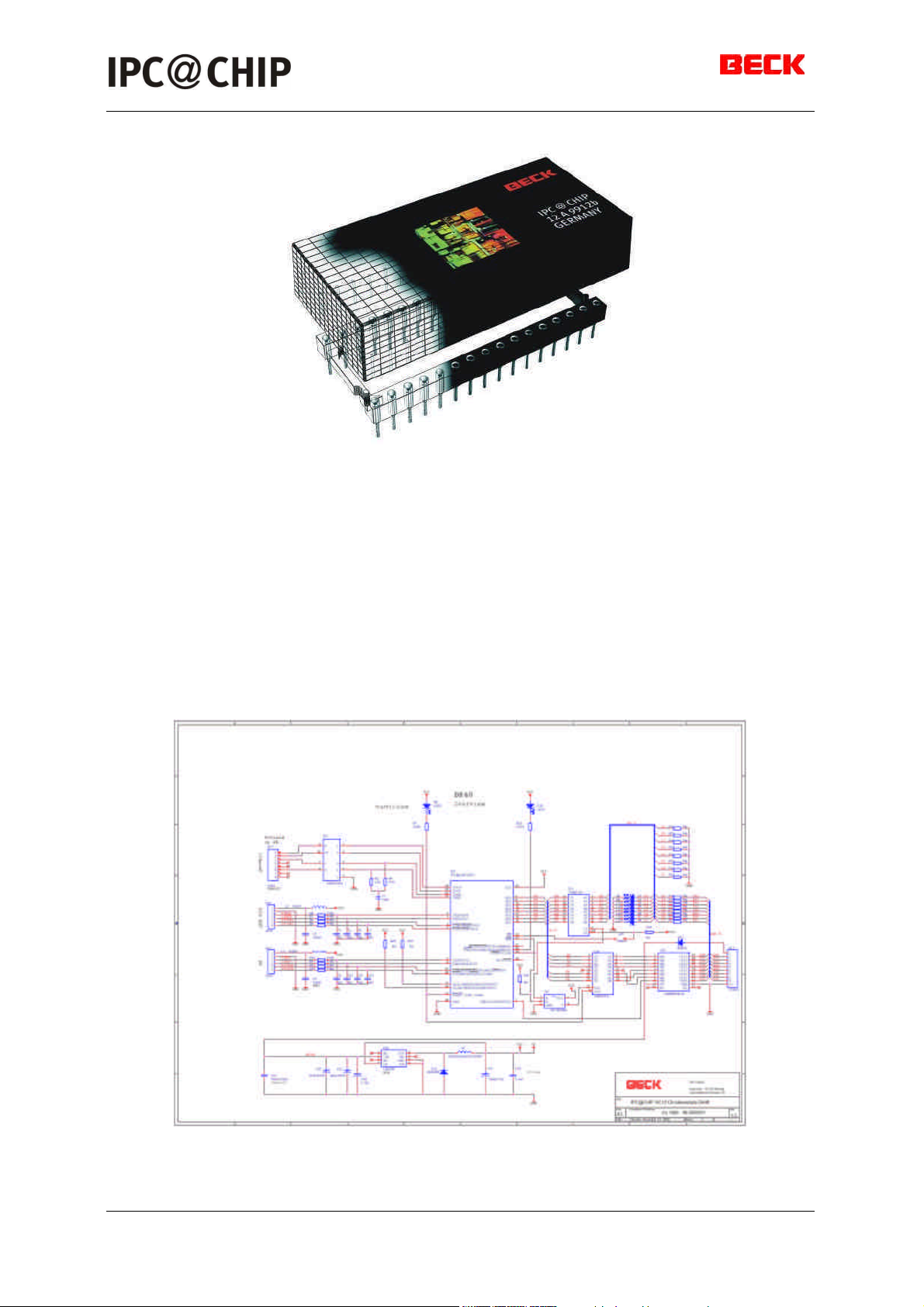
SC01/SC02/SC11/SC12
IPC GmbH
Preliminary
Hardware Manual
High Performance, 80186- and 80188-Compatible,
16-Bit Embedded Microcontroller
Single Chip PC with Ethernet 10Base-T
IPC@CHIP is a registered trademark of BECK IPC GmbH
Sc12hw09.doc page 1 of 37 24.11.1999 V0.9
TF/WB
Page 2

IPC GmbH
SC01/SC02/SC11/SC12
Table of Contents
page
1. BASIC SPECIFICATIONS . . . . . . . 3
2. PHYSICAL DIMENSIONS . . . . . . . 5
3. PIN CONFIGURATION . . . . . . . 5
4. PIN FUNCTIONS . . . . . . . . 6
4.1 Address / Data bus . . . . . . . 6
4.2 Programmable I/O Pins . . . . . . 7
4.3 Programmable Chip Selects . . . . . . 7
4.4 Interrupts . . . . . . . . 8
4.5 Timer . . . . . . . . . 8
4.6 10Base-T Interface . . . . . . . 9
4.7 Asynchronous Serial Ports . . . . . . 9
4.8 DMA . . . . . . . . . 10
4.9 Synchronous Peripheral Interface (SPI) . . . . 10
4.10 I2C-Bus . . . . . . . . 10
4.11 Reset, Power Fail Generator. . . . . . 10
5. FUNCTIONS THAT ARE MUTUAL EXCLUSIVE . . . . 12
6. SYSTEM OVERVIEW . . . . . . . . 14
6.1 Memory map . . . . . . . . 14
6.2 System interrupts . . . . . . . 14
7. CHARACTERISTICS . . . . . . . . 15
8. APPLICATION EXAMPLES . . . . . . . 16
8.1 Evaluation board DK40 . . . . . . 17
8.2 BECK FEC-FC34 . . . . . . . 18
8.2 Power-fail / Reset-out . . . . . . 19
8.3 NMI / Reset-in . . . . . . . 20
8.4 Link- and Traffic-LED. . . . . . . 21
9. HOW TO CONNECT ? . . . . . . . . 22
9.1 256x 8bit I/O-Extension using 74HCT373/245 . . . 23
9.2 8255 24bit I/O and 8254 timer/counter . . . . 24
9.3 Multimeter ADC MAX133CPL . . . . . 25
9.4 8259 peripheral interrupt controller . . . . 26
9.5 16C452/552 UART and printer port. . . . . 27
9.6 16C452/552 without additional address latch . . . 28
9.7 8250 UART with multiplexed address/data bus . . . 29
9.8 8251 UART . . . . . . . . 30
9.9 low-cost 8bit ADC . . . . . . . 31
9.10 µPD7004 up to 16x 10bit ADC . . . . . 32
9.11 DAC4815 4x 12bit . . . . . . . 33
9.12 LC-display . . . . . . . . 34
9.13 Ethernet to Ethernet router . . . . . . 35
9.14 compact flash disk 8bit . . . . . . 36
9.15 82527 CAN bus master . . . . . . 37
Sc12hw09.doc page 2 of 37 24.11.1999 V0.9
TF/WB
Page 3
IPC GmbH
SC01/SC02/SC11/SC12
1. BASIC SPECIFICATIONS
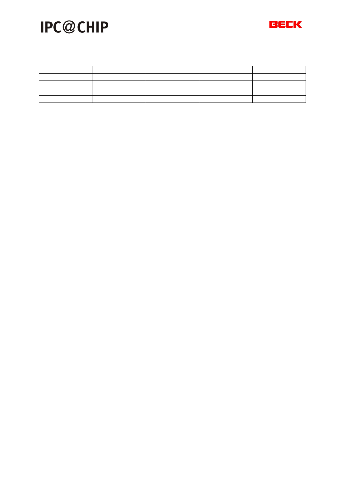
@CHIP CPU RAM FLASH Ethernet
SC01 80188 20MHz 128 Kbyte 128 Kbyte No
SC02 80188 20MHz 128 Kbyte 128 Kbyte 10Base-T
SC11 80186 20MHz 512 Kbyte 512 Kbyte No
SC12 80186 20MHz 512 Kbyte 512 Kbyte 10Base-T
IPC@CHIP® family 80186- and 80188-compatible
microcontroller with up to 512KB-RAM, 512KB-Flash and Ethernet on Chip
- Lower system cost with higher performance
High performance
- 20-MHz operating frequencies
- Zero-wait-state operation at 20 MHz
- 1-Mbyte internal memory space
- 6 x 256-byte I/O space
- Low-power CMOS process with single 5V power supply
Enhanced integrated peripherals
- 14 programmable I/O (PIO) pins
- Two full-featured asynchronous serial ports allow full-duplex, 7-bit, 8-bit, or 9-bit data
transfers, Serial port hardware handshaking with CTS,RTS, ENRX, and RTR selectable
for each port
Improved serial port operation enhances 9-bit DMA support
Independent serial port baud rate generators
DMA to and from the serial ports
- Ethernet controller for IEEE 802.3, 10Base-T,
Integrated 10Base-T transceiver (SC02 and SC12 only)
Auto-Polarity detection and correction
Loopback capability for diagnostics
Receiver and collision squelch circuit to reduce noise
Built-in pre-distortion resisters for 10Base-T application
- Watchdog timer
- Pulse-width demodulation option
- Reset configuration register
Familiar 80C186 peripherals
- Two independent DMA channels
- Programmable interrupt controller with up to six external and eight internal interrupts
- Three programmable 16-bit timers
- Programmable memory and peripheral chip-select logic
Software-compatible with the 80C186 and
80C188 microcontrollers with widely available
native development tools, applications, and
system software
Available in the following packages:
- 32-pin, plastic pack (DIL32)
Sc12hw09.doc page 3 of 37 24.11.1999 V0.9
TF/WB
Page 4
IPC GmbH
8 Bit Address-/Databus
The @CHIP SC01/SC02/SC11/SC12 microcontrollers are part of the Beck IPC@CHIP®
family of System on Chip microcontrollers and microprocessors based on the x86
architecture. The IPC@CHIP family microcontroller is the ideal upgrade for 80C186/188
designs requiring 80C186/188 compatibility, increased performance, serial
communications, Ethernet communications, a direct bus inter-face, and more than 64K of
memory.
The IPC@CHIP family microcontrollers integrates up to 512Kbyte DRAM with increased
performance and up to 512Kbyte FLASH in reducing memory subsystem costs.
The IPC@CHIP family microcontrollers also integrates the functions of the CPU,
multiplexed address bus, three timers, watchdog timer, chip selects, interrupt controller,
two DMA controllers, two asynchronous serial ports, programmable bus sizing, and programmable I/O (PIO) pins on one chip.
The @CHIP SC11/SC12 microcontroller is a highly integrated design that provides all
Media Access Control (MAC) and Encode-Decode (ENDEC) functions in accordance with
the IEEE 802.3 standard. Network interfaces including 10Base-T via the Twisted-pair. The
integrated 10Base-T transceiver makes @Chip SC11/SC12 more cost-effective.
Compared to the 80C186/188 microcontrollers, the IPC@CHIP family microcontrollers
enables designers to reduce the size, power consumption, and cost of embedded
systems, while increasing reliability, functionality, and performance.
The IPC@CHIP family microcontrollers has been designed to meet the most common
requirements of embedded products developed for the communications, office
automation, mass storage, and general embedded markets. Specific applications
including industrial controls, data collection, protocoll conversion, process monitoring and
internet connectivity.
SC01/SC02/SC11/SC12
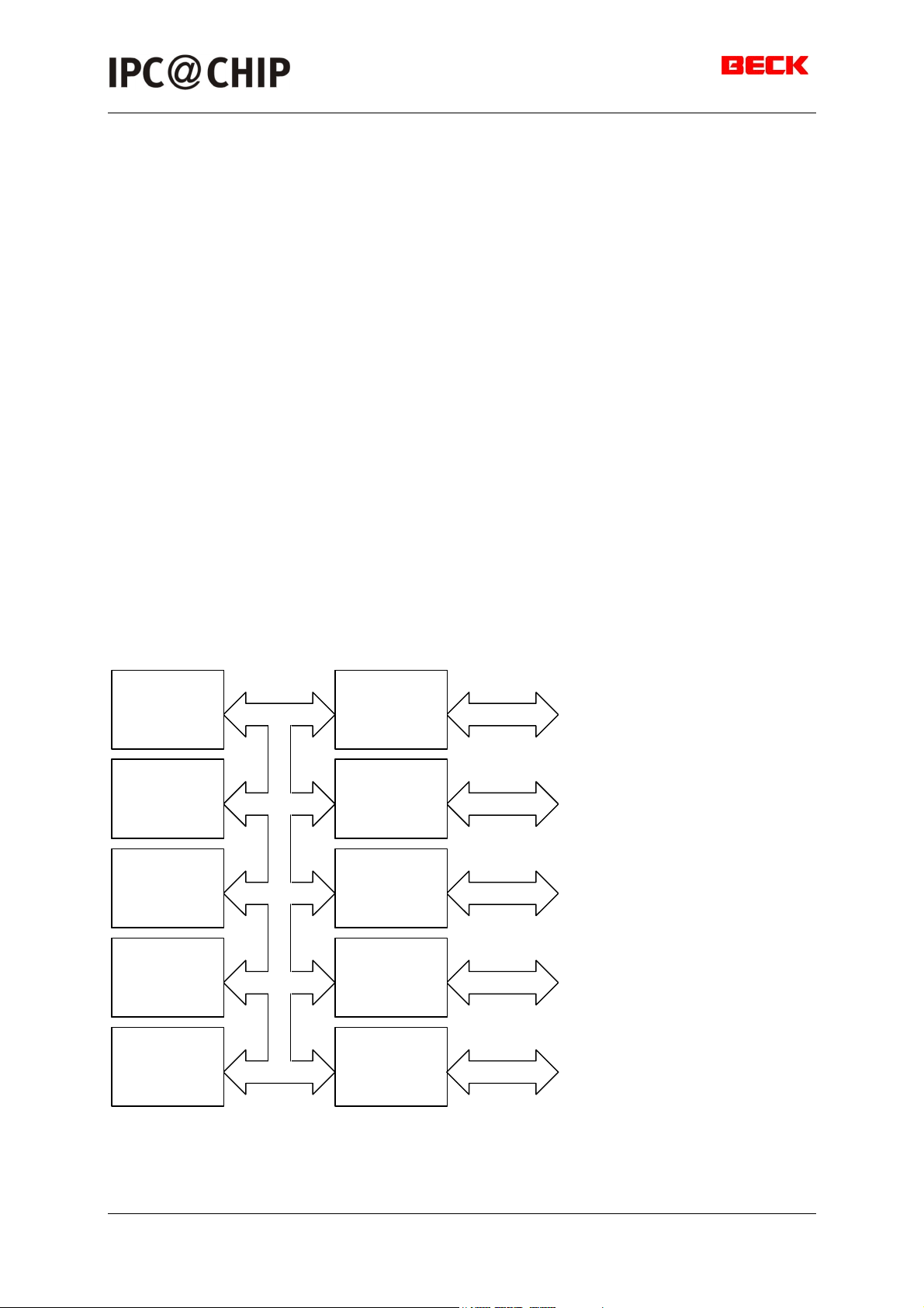
IPC@CHIP family microntroller block diagram
Oscilator
20MHz
Ethernet
MAC
Flash
512Kx8
128Kx8
DRAM
256Kx16
128Kx8
WATCH
DOG
CPU
80186
80188
Ethernet
PHY
UART
DMA
CORE
LOGIC
AD[0..7], ALE
A[0..2], RD#, WR#
INT[0,2..4], INTA#
10Base-T
TPTX+, TPTXTPRX+, TPRXLink/Traffic LED
TxD[0..1], RxD[0..1]
CTS[0..1], RTS[0..1]
ENRX0, RTR0
DRQ[0..1]
Programmable I/O
PIO[0..13]
PCS[0..3,5..6]
TMRIN[0..1]
TMROUT[0..1]
RESET#, NMI
Sc12hw09.doc page 4 of 37 24.11.1999 V0.9
TF/WB
Page 5
IPC GmbH
1 32
2
31
3
30
4
29
5
28
6
IPC@CHIP
27
7
26
8
25
9
24
10
23
11
22
12
21
13
20
14
19
15
18
16
17
SC01/SC02/SC11/SC12
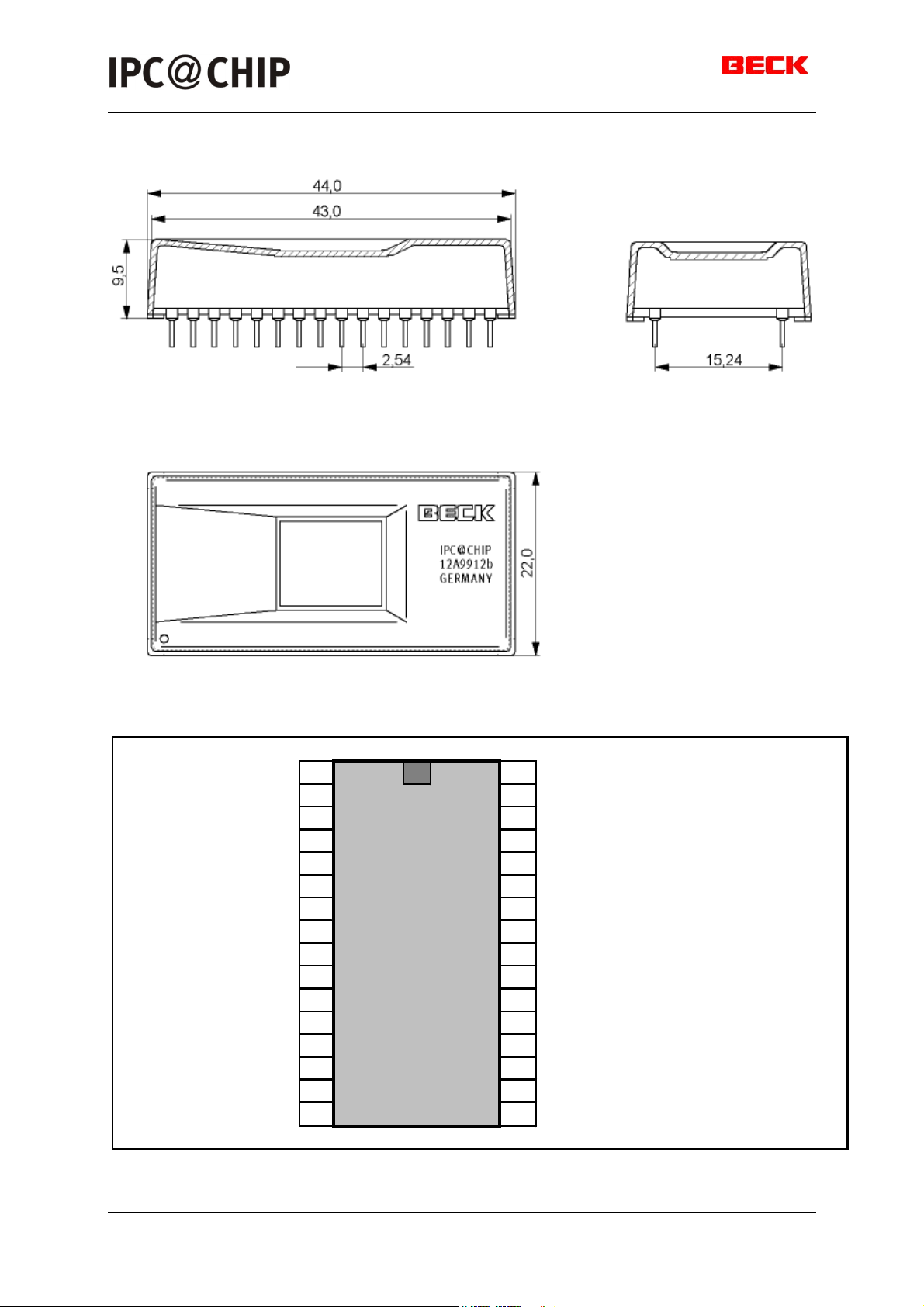
2. PHYSICAL DIMENSIONS
3. PIN CONFIGURATION
PIO7 / RXD0
PIO8 / TXD0
PIO9 / ENRX0 / CTS0
PIO10 / RTR0 / RTS0
PIO11 / TXD1
PIO12 / INT3 / RXD1
PIO13 / INT0 / TMROUT0
AD0
AD1
AD2
AD3
AD4
AD5
AD6
AD7
GND
VCC
I2CCLK / MSCK / DRQ1 / INT6 / PIO0
I2CDAT / MISO / DRQ0 / INT5 / PIO1
A2 / PCS6# / PIO2
A1 / PCS5# / TMRIN1 / TMROUT1 / PIO3
A0 / PCS1# / TMRIN0 / PIO4
RTS1# / MOSI / PCS3# / INT4 / PIO5
CTS1# / MEN / PCS2# / INT2 / INTA# / PIO6
ALE / PCS0#
WR#
RD#
TPRX- (SC02, SC12 only)
TPRX+ (SC02, SC12 only)
TPTX- (SC02, SC12 only)
TPTX+ (SC02, SC12 only)
RESET# / NMI / LINK LED
Sc12hw09.doc page 5 of 37 24.11.1999 V0.9
TF/WB
Page 6
IPC GmbH
SC01/SC02/SC11/SC12
4. PIN FUNCTIONS
Pins That Are Used by Emulators
The following pins are used by emulators for debugging purposes: TxD0, RxD0
Pin Terminology
The following terms are used to describe the pins:
Input (I) - An input-only pin.
Output (O) - An output-only pin.
Input/Output (I/O) - A pin that can be either input or output.
Synchronous - Synchronous inputs must meet setup and hold times in relation to CLK.
Synchronous outputs are synchronous to CLK.
Asynchronous - Inputs or outputs that are asynchronous to CLK.
4.1 Address / Data bus
Pin Name Type Function
A[0..2] O Address Bus (output, three-state, synchronous)
These pins supply nonmultiplexed memory or I/O addresses to
the system one half of a CLK period earlier than the multiplexed
address and data bus (AD7–AD0). During a bus hold or reset
condition, the address bus is in a high-impedance state.
While the IPC@CHIP family microntroller directly interfacing
DRAM, A2–A0 will serve as the nonmultiplexed address bus for
external SRAM, FLASH, PROM, EPROM, and peripherals.
AD[0..7] I/O Multiplexed Address and Data Bus (input/output, three-
state, synchronous, level-sensitive)
These time-multiplexed pins supply partial memory or I/O
addresses, as well as data, to the system. This bus supplies the
low-order 8 bits of an address to the system during the first
period of a bus cycle (t1), and it supplies data to the system
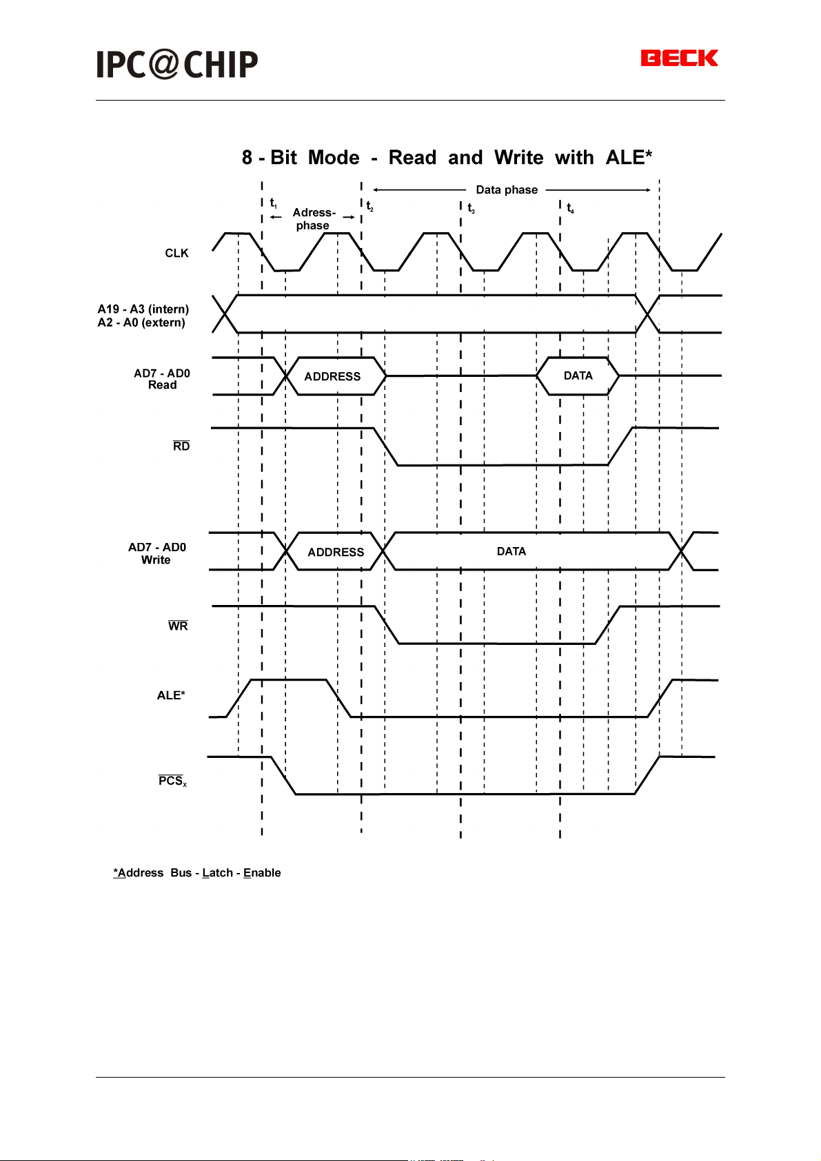
during the remaining periods of that cycle (t2 , t3 , and t4). In 8bit mode, AD7–AD0 supplies the data for both high and low bytes.
The address phase of these pins can be disabled.
During a bus hold or reset condition, the address and data bus is
in a high-impedance state.
ALE O Address Latch Enable (output, synchronous)
This pin indicates to the system that an address appears on the
address and data bus (AD7–AD0). The address is guaranteed to
be valid on the trailing edge of ALE. This pin is three-stated during
ONCE mode.
ALE is three-stated and held resistively Low during a bus hold
condition. In addition, ALE has a weak internal pulldown resistor
that is active during reset, when it is enabled by software.
RD# O Read Strobe (output, synchronous, three-state)
This pin indicates to the system that the microcontroller is
performing a memory or I/O read cycle. RD is guaranteed to not
be asserted before the address and data bus is floated during the
address-to-data transition. RD floats during a bus hold condition.
WR# O Write Strobe (output, synchronous)
This pin indicates to the system that the data on the bus is to be
written to a memory or I/O device. WR floats during a bus hold or
reset condition.
Sc12hw09.doc page 6 of 37 24.11.1999 V0.9
TF/WB
Page 7
IPC GmbH
SC01/SC02/SC11/SC12
4.2 Programmable I/O Pins
Pin Name Type Function
PIO[0..13] I/O Programmable I/O Pins (input/output, asynchronous,
open-drain)
The IPC@CHIP family microcontroller provides 14 individually
programmable I/O pins. Each PIO can be programmed with the
following attributes: PIO function (enabled/disabled), direction
(input/output), and weak pullup or pulldown.
PIO##After power-on reset, the PIO
pin defaults to
0 Input without pullup
1 Input without pullup
2 PCS6# pullup
3 Input with pullup pullup / pulldown
4 Input with pullup pullup
5 Output high pullup
6 Input with pullup pullup
7 RxD0 pullup
8 TxD0 pullup
9 Input with pullup pullup
10 Output high pullup
11 TxD1 pullup
12 RxD1 pullup
13 Output low pulldown
programmable as
Input with
4.3 Programmable Chip Selects
Pin Name Type Function
PCS[0..3] O Peripheral Chip Selects (output, synchronous)
These pins indicate to the system that an I/O memory access is in
progress to the corresponding region of the peripheral memory.
PCS3–PCS0 are three-stated and held resistively High during a
bus hold condition. In addition, PCS3–PCS0 each have a weak
internal pullup resistor that is active during reset. The PCS
outputs assert with the multiplexed AD address bus. Note also
that each peripheral chip select asserts over a 256-byte address
range, which is twice the address range covered by peripheral
chip selects in the 80C186 and 80C188 microcontrollers. PCS3–
PCS0 also have extended wait state options, default is 15 wait
states.
PCS[5..6] O Peripheral Chip Selects (output, synchronous)
These pins indicate to the system that an I/O memory access is in
progress to the corresponding region of the peripheral memory.
PCS6–PCS5 are three-stated and held resistively High during a
bus hold condition. In addition, PCS6–PCS5 each have a weak
internal pullup resistor that is active during reset. The PCS
outputs assert with the multiplexed AD address bus. Note also
that each peripheral chip select asserts over a 256-byte address
range, which is twice the address range covered by peripheral
chip selects in the 80C186 and 80C188 microcontrollers. PCS6–
PCS6 also have extended wait state options, default is 3 wait
states, on SC02 and SC12 changing is not allowed.
Sc12hw09.doc page 7 of 37 24.11.1999 V0.9
TF/WB
Page 8
IPC GmbH
SC01/SC02/SC11/SC12
4.4 Interrupts
Pin Name Type Function
INT[0,2-4] I Maskable Interrupt Request (input,asynchronous)
These pins indicate to the microcontroller that an interrupt
request has occurred. If the INT pin is not masked, the
microcontroller transfers program execution to the location
specified by the corresponding INT vector in the microcontroller
interrupt vector table.
Interrupt requests are synchronized internally and can be edgetriggered or level-triggered. To guarantee interrupt recognition,
the requesting device must continue asserting INT until the
request is acknowledged. INT2 becomes INTA when INT0 is
configured in cascade mode.
INTA# O Interrupt Acknowledge (output, synchronous)
When the microcontroller interrupt control unit is operating in
cascade mode, this pin indicates to the system that the
microcontroller needs an interrupt type to process the interrupt
request on INT0. The peripheral issuing the interrupt request
must provide the microcontroller with the corresponding interrupt
type.
PWD Pulse Width Demodulator (input, Schmitt trigger)
If pulse width demodulation is enabled, PWD processes a signal
through the Schmitt trigger. PWD is used internally to drive
TMRIN0 and INT2, and PWD is inverted internally to drive
TIMERIN1 and INT4. If INT2 and INT4 are enabled and timer 0
and timer 1 are properly configured, the pulse width of the
alternating PWD signal can be calculated by comparing the values
in timer 0 and timer 1.
In PWD mode, the signals TMRIN0, TMRIN1 and INT4 can be used
as PIOs. If they are not used as PIOs, they are ignored internally.
4.5 Timer
Pin Name Type Function
TMRIN[0..1] I Timer Input (input, synchronous, edge-sensitive)
These pins supply a clock or control signal to the internal
microcontroller timer 0 and 1. After internally synchronizing a
Low-to-High transition on TMRIN, the microcontroller increments
the corresponding timer. TMRIN must be tied High if not being
used. When PIO is enabled, TMRIN is pulled High internally.
TMRIN0 is driven internally by INT2/PWD when pulse width
demodulation mode is enabled. The TMRIN0 pin can be used as a
PIO when pulse width demodulation mode is enabled.
TMROUT[0..1] O Timer Output (output, synchronous)
These pins supplies the system with either a single pulse or a
continuous waveform with a programmable duty cycle. TMROUT is
floated during a bus hold or reset.
Sc12hw09.doc page 8 of 37 24.11.1999 V0.9
TF/WB
Page 9
IPC GmbH
SC01/SC02/SC11/SC12
4.6 10Base-T Interface
Pin Name Type Function
TPTX[+,-] O Twisted Pair Driver (outputs)
These two outputs provide the TP drivers with pre-distortion
capability
TPRX[+,-] I Twisted Pair Receive (inputs).
A differential receiver tied to the receive transformer pair of the
twisted-pair wire.
The receive pair of the twisted-pair medium is driven with 10
Mbits/s Manchester-encoded data
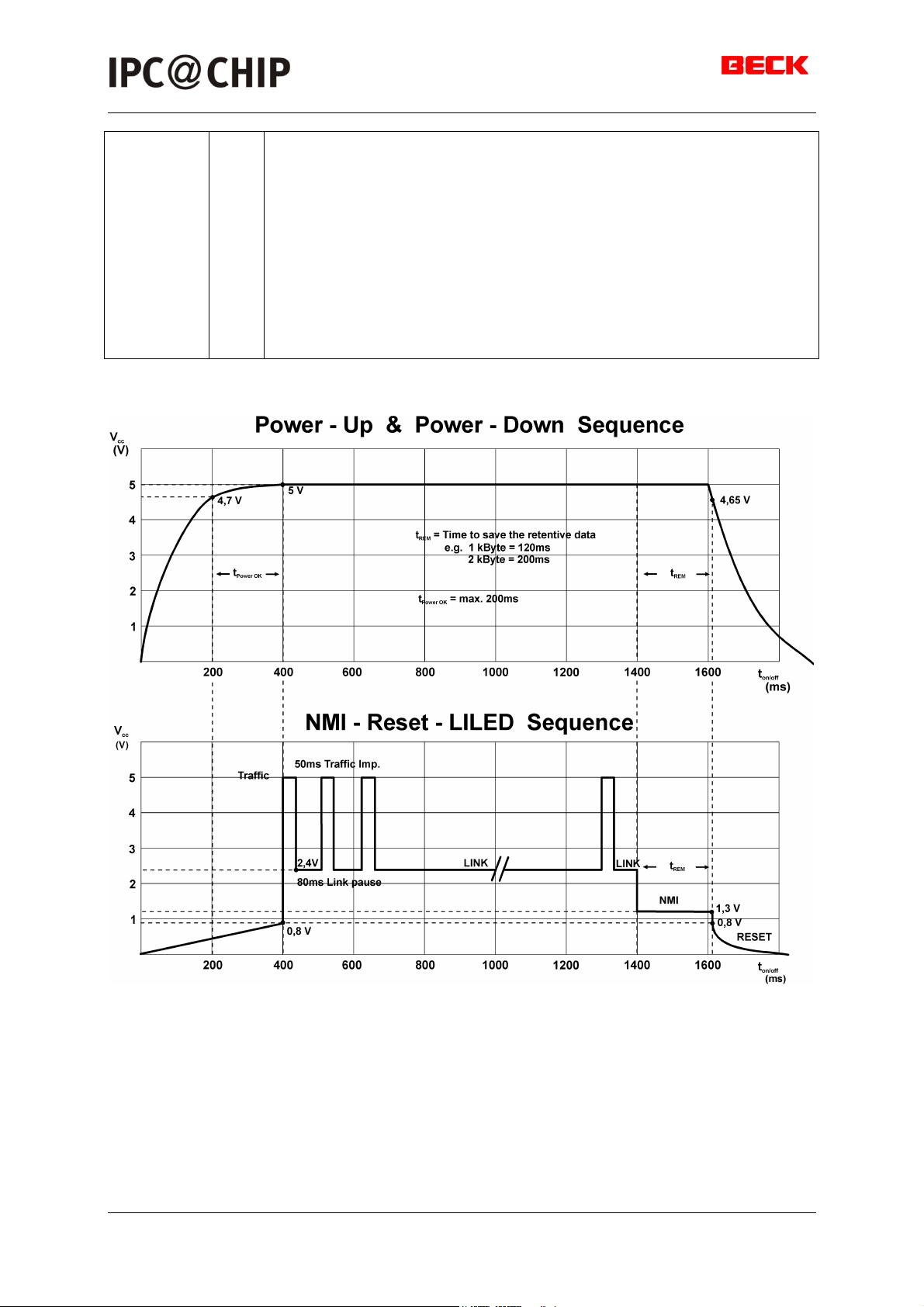
LINK LED O Link and Traffic LED Driver (output)
If TP is LINK-pass, this pin outputs 2.5V.
This pin will output 5V for 80ms to indicate the presence of traffic
on the network.
If no LED / 200Ω combination is connexted to this pin, 1K pullup
should be tied to this pin, to make shure RESET# and NMI
function is available.
4.7 Asynchronous Serial Ports
Pin Name Type Function
TxD[0..1] O Transmit Data (output, asynchronous)
These pins supply asynchronous serial transmit data to
the system from serial port 0 and 1.
RxD[0..1] I Receive Data (input, asynchronous)
These pins supply asynchronous serial receive data from the
system to asynchronous serial ports 0 and 1.
CTS[0..1] I Clear-to-Send (input, asynchronous)
These pins provide the Clear-to-Send signal for asynchronous
serial port 0 and 1 when hardware flow control is enabled for the
port. The CTS signals gate the transmission of data from the
associated serial port transmit register. When CTS is asserted, the
transmitter begins transmission of a frame of data, if any is
available. If CTS is deasserted, the transmitter holds the data in
the serial port transmit register. The value of CTS is checked only
at the beginning of the transmission of the frame.
ENRX0 I Enable-Receiver-Request 0 (input, asynchronous)
This pin provides the Enable Receiver Request for asynchronous
serial port 0 when hardware flow control is enabled for the port.
The ENRX0 signal enables the receiver for the associated serial
port.
RTS[0..1] O Ready-to-Send 0 (output, asynchronous)
These pins provide the Ready-to-Send signal for asynchronous
serial ports 0 and 1 when hardware flow control is enabled for the
port. The RTS signals are asserted when the associated serial port
transmit register contains data that has not been transmitted.
RTR0 O Ready-to-Receive 0 (output, asynchronous)
This pin provides the Ready-to-Receive signal for asynchronous
serial port 0 when hardware flow control is enabled for the port.
The RTR0 signal is asserted when the associated serial port
receive register does not contain valid, unread data.
Sc12hw09.doc page 9 of 37 24.11.1999 V0.9
TF/WB
Page 10
IPC GmbH
SC01/SC02/SC11/SC12
4.8 DMA
Pin Name Type Function
DRQ[0..1] I DMA Request (input, synchronous, level-sensitive)
These pins indicate to the microcontroller that an external device
is ready for DMA channel 0 or 1 to perform a transfer. DRQ0 is
edge-triggered and internally synchronized. DRQ is not latched
and must remain active until serviced.
4.9 Synchronous Peripheral Interface (SPI)
Pin Name Type Function
MEN O Not implemented yet
MSCK O Not implemented yet
MISO I Not implemented yet
MOSI O Not implemented yet
4.10 I2C-Bus
Pin Name Type Function
I2CCLK O I2C-Bus Clock (output)
This pin provides clock to an external I2C slave.
I2CDAT I/O I2C-Bus Data in/out (input/output)
This pin acts either as data input or data output. The IPC@CHIP
family microntroller handles up to 127 external slaves. Itself is
always master and cannot addressed as slave.
4.11 Reset, Power Fail Generator
Pin Name Type Function
RESET# I/O Reset (input/output, asynchronous, level-sensitive)
If voltage on this pin goes down below 0.8V this pin requires the
microcontroller to perform a reset. When RESET is asserted, the
microcontroller immediately terminates its present activity, clears it’s
internal logic, and transfers CPU control to the reset address,
FFFF0h.
If Vcc goes down below 4.5V or internal watchdog is released this
pin will be driven to GND.
NMI I Nonmaskable Interrupt (input, synchronous, edge-sensitive)
If voltage on this pin goes down below 1.5V it indicates to the
microcontroller that an interrupt request has occurred. The NMI
signal is the highest priority hardware interrupt and, unlike the
INT6–INT0 pins, cannot be masked. The microcontroller always
transfers program execution to the location specified by the
nonmaskable interrupt vector in the microcontroller interrupt vector
table when NMI is asserted.
Although NMI is the highest priority interrupt source, it does not
participate in the priority resolution process of the maskable
interrupts. There is no bit associated with NMI in the interrupt inservice or interrupt request registers. This means that a new NMI
request can interrupt an executing NMI interrupt service routine. As
Sc12hw09.doc page 10 of 37 24.11.1999 V0.9
TF/WB
Page 11
IPC GmbH
with all hardware interrupts, the IF (interrupt flag) is cleared when
the processor takes the interrupt, disabling the maskable interrupt
sources. However, if maskable interrupts are re-enabled by software
in the NMI interrupt service routine, via the STI instruction for
example, the fact that an NMI is currently in service does not have
any effect on the priority resolution of maskable interrupt requests.
For this reason, it is strongly advised that the interrupt service
routine for NMI should not enable the maskable interrupts. An NMI
transition from Low to High is latched and synchronized internally,
and it initiates the interrupt at the next instruction boundary. To
guarantee that the interrupt is recognized, the NMI pin must be
asserted for at least one CLK period.
SC01/SC02/SC11/SC12
Sc12hw09.doc page 11 of 37 24.11.1999 V0.9
TF/WB
Page 12
IPC GmbH
SC01/SC02/SC11/SC12
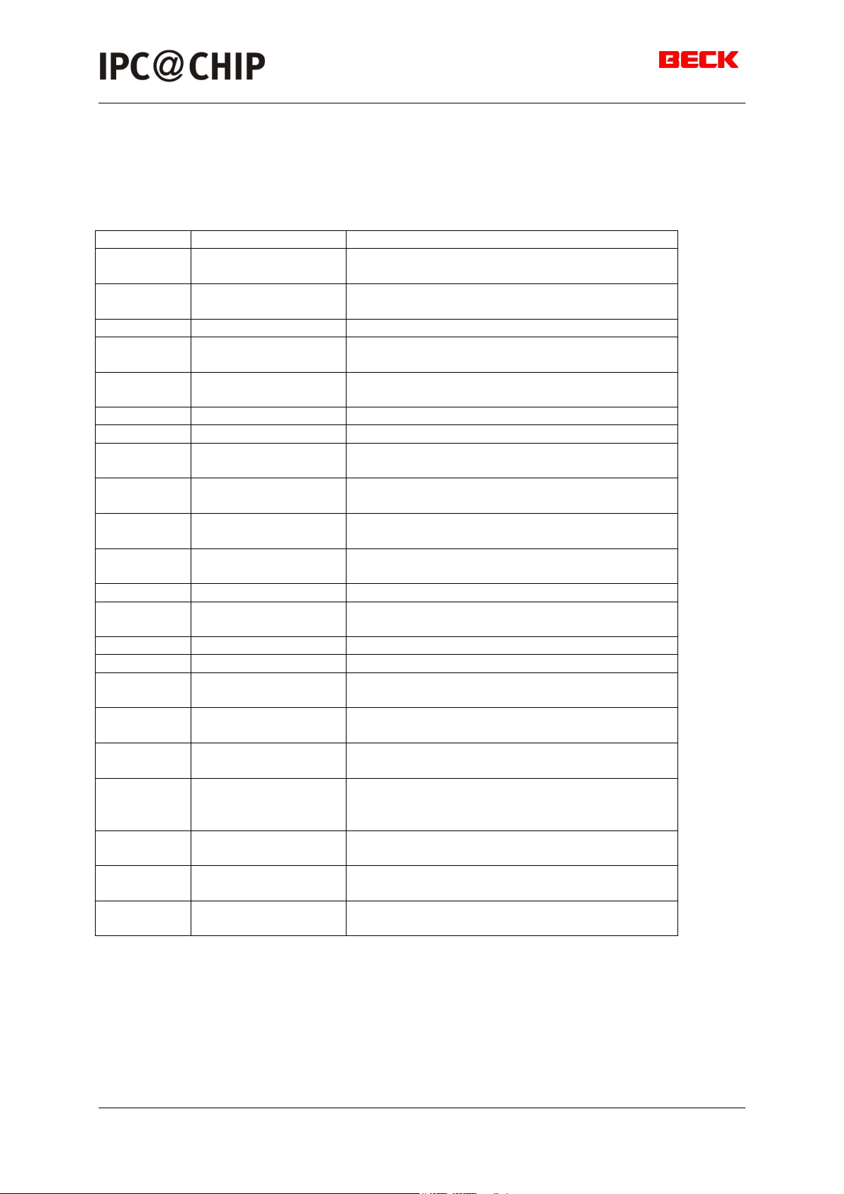
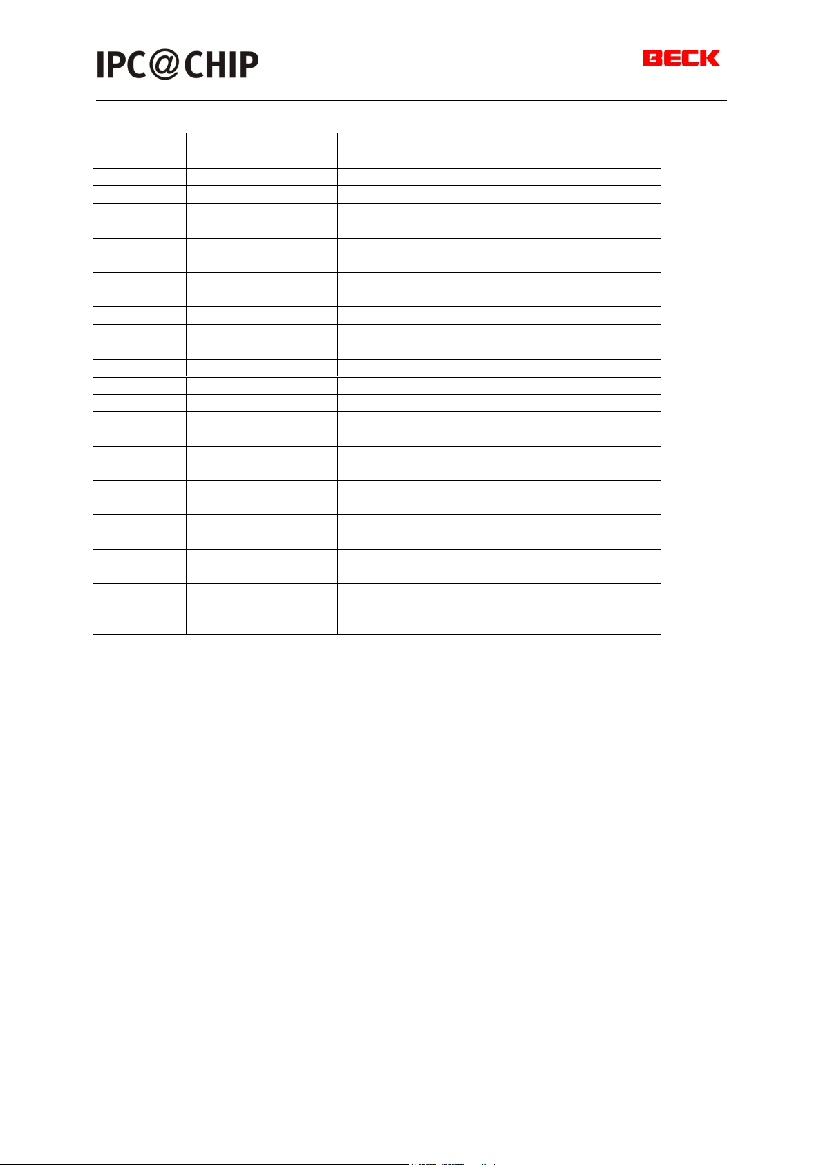
5. FUNCTIONS THAT ARE MUTUAL EXCLUSIVE
The IPC@CHIP family microcontroller provides a lot of different functions by several
multi-function pins. Choosing one function will result in disabling other functions. The
following table shows, which functions are mutual exclusive.
Pin Name Function Exclusion
A0 nonmultiplexed
address A0
A[1..2] nonmultiplexed
address A[1..2]
ALE Address / Data bus PCS0#
CTS0 /
ENRX0#
CTS1 hardware flow
DRQ0 DMA Request 0 PIO1, INT5, I2C-Bus, SPI
DRQ1 DMA Request 1 PIO0, INT6, I2C-Bus, SPI
I2CCLK,
I2CDAT
INT0 Interrupt Request 0 PIO13, TMROUT0, cascaded Interrupt
INT0 cascaded Interrupt
INT2 Interrupt Request 2 PIO6, PCS2#, INTA#, PWD, SPI, hardware
INT3 Interrupt Request 3 PIO12, Serial Port 1
INT4 Interrupt Request 4 PIO5, PCS3#, SPI, hardware flow control
INT5 Interrupt Request 5 PIO1, DRQ0, I2C-Bus, SPI
INT6 Interrupt Request 6 PIO0, DRQ1, I2C-Bus, SPI
INTA# cascaded Interrupt
PCS0# programmable chip
PCS1# programmable chip
PCS2# programmable chip
PCS3# programmable chip
PCS5# programmable chip
PCS6# programmable chip
hardware flow
control Serial Port 0
control Serial Port 1
I2C-Bus PIO[0..1], DMA, INT[5..6], SPI
Controller
Controller
select 0
select 1
select 2
select 3
select 5
select 6
PIO4, PCS1#, TMRIN0
PIO[2..3], PCS[5..6], Timer 1
PIO9
PIO6, PCS2#, INT2, INTA#, PWD, SPI
Controller
PIO6, PIO13, INT2, PCS2#, PWD, SPI,
TMROUT0, hw flow control Serial Port 1
flow control Serial Port 1
Serial Port 1
PIO6, PIO13, INT0, INT2, PCS2#, PWD,
TMROUT0, SPI, hw flow control Serial Port 1
Address/Data bus
A0, PIO4, TMRIN0, SPI
PIO6, INT2, INTA#, PWD, SPI, hw flow
control Serial Port 1, cascaded Interrupt
Controller
PIO5, INT4, SPI, hardware flow control
Serial Port 1
A[1..2], PIO3, Timer 1
A[1..2], PIO2
continued on next page ...
Sc12hw09.doc page 12 of 37 24.11.1999 V0.9
TF/WB
Page 13
IPC GmbH
Pin Name Function Exclusion
PIO0 programmable I/O DRQ1, INT6, I2C-Bus, SPI
PIO1 programmable I/O DRQ0, INT5, I2C-Bus, SPI
PIO2 programmable I/O A2, PCS6#
PIO3 programmable I/O A1, PCS#, Timer 1
PIO4 programmable I/O A0, PCS1#, TMRIN0, SPI
PIO5 programmable I/O PCS3#, INT4, SPI, hardware flow control
PIO6 programmable I/O PCS2#, INT2, cascaded Interrupt Controller,
PIO7 programmable I/O Serial Port 0
PIO8 programmable I/O Serial Port 0
PIO9 programmable I/O hardware flow control Serial Port 0
PI1O programmable I/O hardware flow control Serial Port 0
PI11 programmable I/O Serial Port 1
PI12 programmable I/O Serial Port 1, INT3
PI13 programmable I/O INT0, cascaded Interrupt Controller,
RxD0, TxD0 Serial Port 0 w/o
hw flow control
RxD0, TxD0
CTS0, RTS0
RxD1, TxD1 Serial Port 1 w/o
RxD1, TxD1
CTS1, RTS1
MEN, MSCK
MISO,MOSI
Serial Port 0 with
hw flow control
hw flow control
Serial Port 1 with
hw flow control
SPI (Synchronous
Peripheral Intf.)
SC01/SC02/SC11/SC12
Serial Port 1
PWD, SPI, hw flow control Serial Port 1
TMROUT0
PIO[7..8]
PIO[7..10]
PIO[11..12], INT3
PIO[5..6,11..12], INT3, PCS[2..3]#, INT2,
INT4, PWD, SPI, cascaded Intrpt. Controller
A0, PIO[0..1,4..5], PCS[1,3]#, INT[2,4..6],
DMA, I2C-Bus, PWD,TMRIN0, hw flow control
Serial Port 1, cascaded Intrpt. Controller
Sc12hw09.doc page 13 of 37 24.11.1999 V0.9
TF/WB
Page 14
IPC GmbH
FFFFFh
00000h
FF00h
Internal Register
PCS0#
PCS1#
PCS2#
PCS3#
PCS5#
PCS6#
SC01/SC02/SC11/SC12
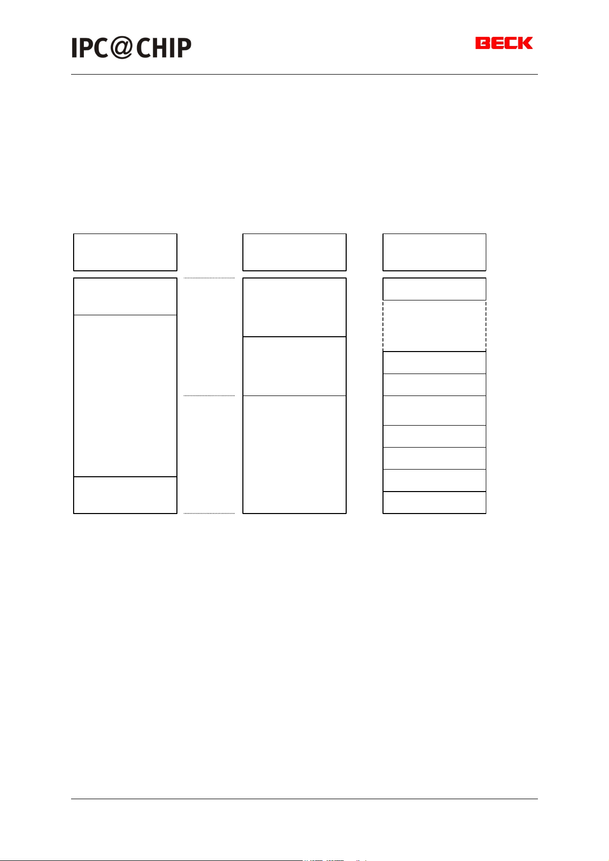
6. SYSTEM OVERVIEW
IPC@CHIP family microcontroller has a system configuration based on the ISA
architecture with some changes: No ISA-Bus, no Video-Interface, no Keyboard Interface,
programming of Serial Ports, DMA, PIC and Timer is different from standard IBM PC.
This section provides an overview of the system memory configuration and basic I/O.
6.1 Memory map
SC01/SC02
Memory
Embedded Code
128Kbyte Flash
Working Memory
128Kbyte RAM
80000h
7FFFFh
SC11/SC12
Memory
Firmware
256Kbyte ROM
Flash Disk
256Kbyte
Working Memory
512Kbyte RAM
I/O map
Ethernet MAC
FFFFh
06FFh
0600h
05FFh
0500h
04FFh
0400h
03FFh
0300h
02FFh
0200h
01FFh
0100h
00FFh
6.2 System interrupts
Interrupt Request 1 is internaly connected to Ethernet MAC and is not available extern.
Sc12hw09.doc page 14 of 37 24.11.1999 V0.9
TF/WB
Page 15
IPC GmbH
SC01/SC02/SC11/SC12
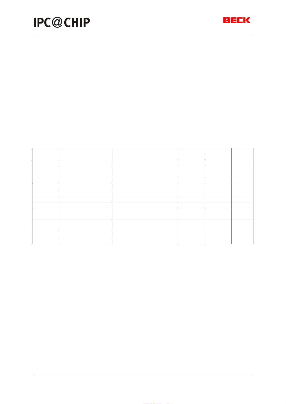
7. CHARACTERISTICS
ABSOLUTE MAXIMUM RATINGS
Storage temperature : -25°C to +70°C see IEC 68-2-1/2
Supply voltage (Vcc) : 5V +/- 10%
Supply current (Vcc = 5,5V) : 400 mA
Voltage on any pin with respect to ground: -0,5V to Vcc + 0,5V
OPERATING RANGES
Operating temperature (Case temp. tc) : 0°C to +55°C
Power supply current @ 20MHz : min. 350mA typ. 380mA max. 400mA
DC-CHARACTERISTICS
Symbol Parameter Test Condition Preliminary Unit
Description MIN. MAX.
IOH = [email protected]
VILO Voltage Input Low - -0.5 Vcc-0.3 V
VIHI Voltage Input High - 2.0 Vcc+0.5 V
VRESLO Voltage Reset Low TTL level with Appl. 1 - 0.8 V
VRESHI Voltage Reset High TTL level with Appl. 1 2.4 Vcc+0.5 V
VPFNMI Voltage Power fail TTL level with Appl. 1 - 0.8 V
VCRT Voltage Serial COM
Receive & Transmit
VICDC Voltage I²C Data &
Clock
VTPRX Voltage TP Receive Input 0.35 2.0 V
VTPTX Voltage TP Transmit Output 0.8 2.4 V
TTL High
TTL Low
TTL High
TTL Low
2.4
Vcc-0.5
2.4
-
2.4
-
Vcc+0.5
Vcc
Vcc+0.5
0.8
Vcc+0.5
0.8
V
V
V
V
V
V
Sc12hw09.doc page 15 of 37 24.11.1999 V0.9
TF/WB
Page 16
IPC GmbH
SC01/SC02/SC11/SC12
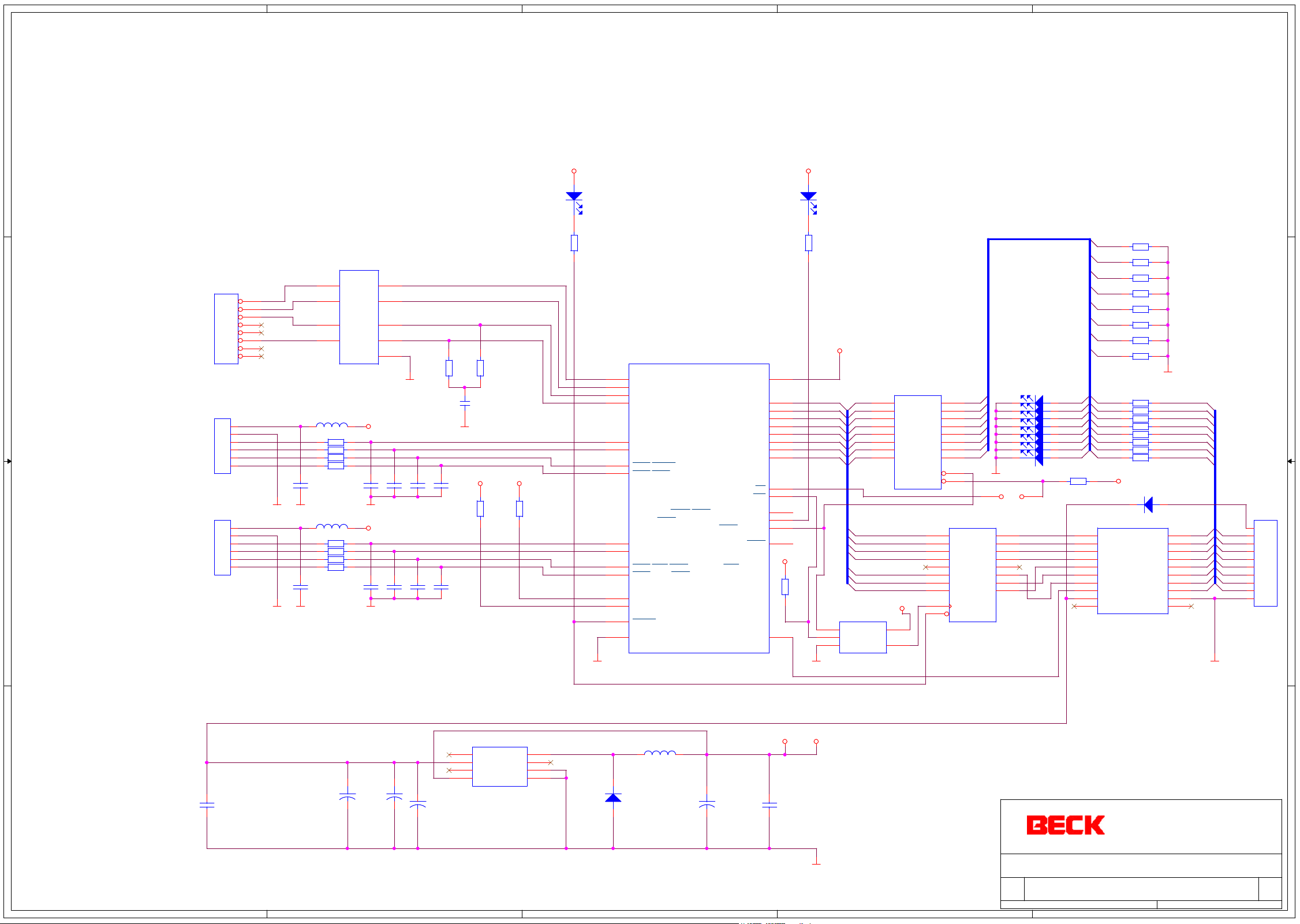
8. APPLICATION EXAMPLES
The following 5 pages contain schematics, showing the IPC@CHIP family microcontroller
in two applications (BECK-IPC GmbH: DK40 and FEC-FC34) and gives you three
solutions, how to handle the multi-function pin 17 RESET# / NMI / LINK-LED.
Sc12hw09.doc page 16 of 37 24.11.1999 V0.9
TF/WB
Page 17
5
D D
4
3
2
1
VCC
D9
Traffic/Link
R1
200R
Schield
on PE
ST1
1
2
3
4
5
6
RJ45
RJ45ST1
ST2
1
2
3
4
5
6
RJ12
ST3
1
2
3
4
5
6
RJ12
7
8
L2 100uH
ETXD0
ECTS0#
ERTS0#
GND
L3 100uH
ETXD1
ERXD1
ECTS1#
ERTS1#
GND
GND
GND
C C
SYS EXT10BaseT
PG
B B
IC1
9
9
10
10
7
7
8
8
FS22101Y4
R6 100R
R7 100R
R8 100R
R9 100R
C3
100nF
R10 100R
R11 100R
R12 100R
R13 100R
C8
100nF
0805
GND
GND
1
2
3
4
5
VCC
C4
2n2
VCC
C9
2n2
1
2
3
4
5
GND
C7
C6
C5
2n2
2n2
2n2
C10
2n2
C11
2n2
C12
2n2
R3
47R
GND
C1
10nF
VCC
R4
47R
R24
4k7
VCC
R25
4k7
LED2
GND
DK40
Overview
IC2
IPC@CHIP SC12
18
TPTX+
19
TPTX-
20
TPRX+
21
TPRX-
2
TXD0/PIO8
1
RXD0/PIO7
3
CTS0/ENRX0/PIO9
4
RTS0/RTR0/PIO10
MCS0/PCS1/PIO4/TMRIN0/A0
PCS5/PIO3/TMROUT1/TMRIN1/A1
5
TXD1/PIO11
6
RXD1/INT3/PIO12
25
CTS1/MEN/PCS2/PIO6/INT2/INTA/PW
26
RTS1/MOSI/PCS3/PIO5/INT4
31
I2CCLK/MSCK/DRQ1/INT6/PIO0
30
I2CDAT/MISO/DRQ0/INT5/PIO1
17
RESET_PFAIL_LILED
16 7
GND TMROUT0/INT0/PIO13
VCC
AD0
AD1
AD2
AD3
AD4
AD5
AD6
AD7
RD
WR
PCS6/PIO2/A2
ALE/PCS0
R22
470R
32
8
9
10
11
12
13
14
15
22
23
27
28
29
24
VCC
VCC
R35
4k7
GND
D10
LED1
VCC
D0
D1
D2
D3
D4 D4
D5
D6ERXD0
D7
D[0..7]
IC7
OR2
1
A
2
B
3 4
GND Y
NC7S32M5
E[0..7]
IC3
74ABT541
D0
18
D1
17
D2
16
D3
15
14
D5
13
D6 E6
12
D7 E7
11
D0
D1
D2
D3
D6
D5
D4
5
VCC
Y1
Y2
Y3
Y4
Y5
Y6
Y7
Y8
VCC
A1
A2
A3
A4
A5
A6
A7
A8
G1
G2
3
4
7
8
13
14
17
18
11
1
2
3
4
5
6
7
8
9
1
19
IC4
D1
D2
D3
D4
D5
D6
D7
D8
CLK
CLR
74ABT273
E0
E1
E2
E3
E4
E5
E6
E7
GND
JP1
JUMP2
2
Q1
5
Q2
6
Q3
9
Q4
12
Q5
15
Q6
16
Q7
19
Q8
E0
D1SL
E1
D2SL
E2 E2
D3LED
E3
D4LED R17 10k
E4
D5LED
E5
D6LED
E6
D7LED
E7
D8LED
R34
4k7
IC5
1
IN1
2
IN2
3
IN3
4
IN4
5
IN5
6
IN6
7
IN7
8
IN8
9 12
VS GND
10 11
NC NC
E0
R26 10k
E1
R27 10k
E2
R28 10k
E3
R29 10k
E4
R30 10k
E5
R31 10k
E6
R32 10k
E7
R33 10k
GND
D11
OUT1
OUT2
OUT3
OUT4
OUT5
OUT6
OUT7
OUT8
20
19
18
17
16
15
14
13
EA0
EA1
EA2
EA3
EA4
EA6
EA7
E0
R14 10k
E1
R15 10k
R16 10k
E3
E4
R18 10k
E5 EA5
R19 10k
R20 10k
R21 10k
VCC
1N4007
UDN2982SLW
EA0
EA1
EA2
EA3
EA4
EA5
EA6
EA7
EA[0..7]
GND
EA0
EA1
EA2
EA3
EA4
EA5
EA6
EA7
KL1
1
2
3
4
5
6
7
8
9
10
CON10
5V
IC6
INT24V
A A
5
C17
100nF/250V
Capacitor
C21
22uF/35VS
+
22uF/35VS
C22
+
0.1uF
4
7
VIN
3 6
NC GND
4 5
FB /ON
LM2594
SO8
81
OUTNC
2
NC
D12
30BQ040
L4
220uH/500mA/DO3308P
C15
+
100uF/10VC19
3
VCC
C20
0.1uF
5V/500mA
GND
IPC GmbH
Germany - 35578 Wetzlar
Garbenheimer Strasse 38
Title
Size Document Number Rev
2
Date: Sheet of
IPC@CHIP SC12 Circuitexample DK40
A3
Tuesday, November 23, 1999
(c) 1996 - 99 DK40D1
1
1
0.8
1
Page 18
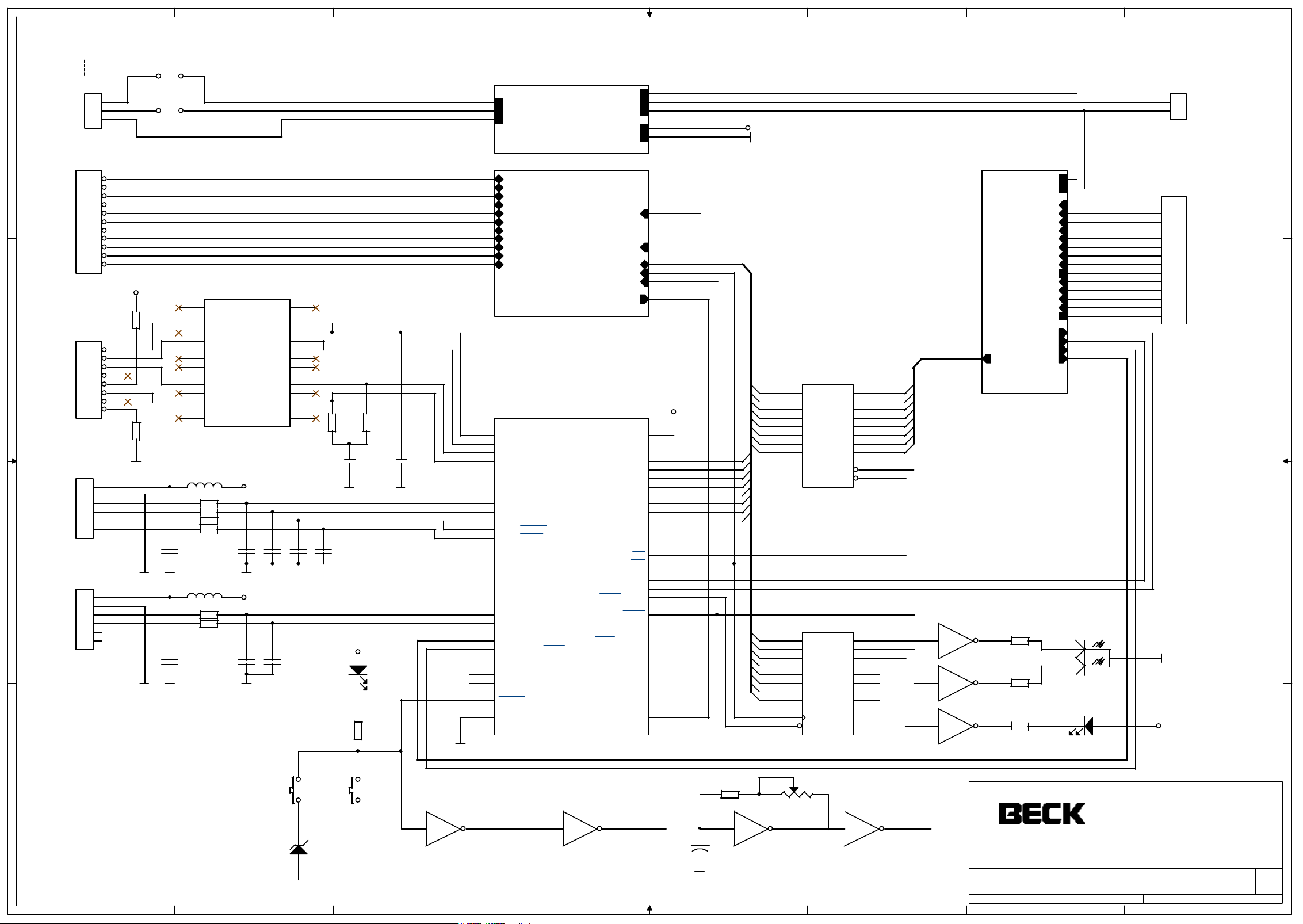
8
7
6
5
4
3
2
1
FC34
BR1
ST3
DC IN PGSYS EXT
D D
980-S-3
ST2
OUT RELAIS
10
11
980-S-11
Schirm
auf PE
ST7
C C
B B
10BaseT
CON8
RJ45ST1
ST45
1
2
3
4
5
6
RJ12
ST1
1
2
3
4
5
6
RJ12
V1
1
V2 IN0V
2
3
A0.01.COM
1
A0.0
2
A0.1
3
A0.2
4
A0.3
5
A0.4
6
A0.5
7
A0.6
8
A0.7
9
A0.2-7.COM
A0.0-7.GND
VCC
R6
0R
1
2
3
4
5
6
7
8
R7
0R
GND
L30 100uH
ETXD0
ERXD0
ECTS0#
ERTS0#
L31 100uH
ETXD1
ERXD1
GND
GND
JUMP2
BR2
JUMP2
19
18
17
16
15
14
13
11
R69 100R
R70 100R
R71 100R
R72 100R
100nF
GND
R? 100R
R? 100R
100nF
GND
IC24
19
18
17
NC
NC
14
13
NC
SF1012
VALORSMD
VCC
C36
2n2
GND
VCC
C?
2n2C?2n2
GND
NCNC
NC
NC
NC
C37
2n2
120
2
2
3
3
4
4
5
6
7
7
8
8
912
912
10
C38
C39
2n2
2n2
LED
Traffic/Link
IN24V OUT24V
PE
R8
R9
47R
47R
R62
470R
C8
10nF
GNDGND
INT2/PWD
INT4
GND
C9
10nF
VCC
L1
NETZTEIL 24V
IN24V
IN0V
PE
FC34D1B
Ausgabe-Elektronik
A0.01.COM
A0.0
A0.1
A0.2
A0.3
A0.4
A0.5
A0.6
A0.7
A0.2-7.COM
A0.0-7.GND D[0..15]
FC34D1D
IC?
IPC@CHIP SC12
18
TPTX+
19
TPTX-
20
TPRX+
21
TPRX-
2
TXD0/P8
1
RXD0/P7
3
CTS0/ENRX0/P9
4
RTS0/RTR0/P10
MCS0/PCS1/P4/TMRIN0/A0
PCS5/P3/TMROUT1/TMRIN1/A1
5
TXD1/P11
6
RXD1/INT3/P12
25
CTS1/MEN/PCS2/P6/INT2/INTA/PW
26
RTS1/MOSI/PCS3/P5/INT4
31
I2CCLK/MSCK/DRQ1/INT6/P0
30
I2CDAT/MISO/DRQ0/INT5/P1
17
RESET_PFAIL_LILED
16 7
GND TMROUT0/INT0/P13
REL24V
OUT24V
OUT0V
5V
0V
RESET#
TMROUT0
WR#
PCS3#
DIAG
VCC
AD0
AD1
AD2
AD3
AD4
AD5
AD6
AD7
RD
WR
PCS6/P2/A2
ALE/PCS0
RESET#
WD#
PCS0#
P10
VCC
32
8
9
10
11
12
13
14
15
22
23
27
28
29
24
D0
D1
D2
D3
D4
D5
D6
D7
RD#
WR#
TMRIN0
TMRIN1
PCS6#
PCS0#
P10
REL24V
OUT0V
VCC
GND
D0
D1
D2
D3
D4
D5
D6
D7
D0
D1
D2
D3
D4
D5
D6
D7
IC?
74AHCT541
18
17
16
15
14
13
12
11
3
4
7
8
13
14
17
18
11
1
Y1
Y2
Y3
Y4
Y5
Y6
Y7
Y8
IC?
D1
D2
D3
D4
D5
D6
D7
D8
CLK
G
74HCT377
A1
A2
A3
A4
A5
A6
A7
A8
G1
G2
Q1
Q2
Q3
Q4
Q5
Q6
Q7
Q8
DC
ST4
2
1
980-S-2
Eingabe-Elektronik
REL24V
OUT0V
E0.0
E0.1
E0.2
E0.3
E0.4
E0.5
E0.6
E0.7
E0.COM
E1.0
E1.1
E1.2
E1.3
E1.COM
TMRIN1
TMRIN0
R60
390E
R61
390E
R58
390E
INT2
INT4
E[0..7]
E0
2
E1
3
4
E2
E3
5
E4
6
E5
7
E6
8
E7
9
PCS0#
1
RD#
19
2
5
6
9
12
15
16
19
13 12
11 10
9 8
FC34D1A
POWER
* GRUEN+ROT PG DOWNLOAD
IC15F
74HCT14
IC15E
74HCT14
IC15D
74HCT14
E0.0
E0.1
E0.2
E0.3
E0.4
E0.5
E0.6
E0.7
E0.COM
E1.0
E1.1
E1.2
E1.3
E1.COM
TMRIN1
TMRIN0
INT2/PWD
INT4
D7
DUOLED
DUOLED5
ERROR
D6
LED
ST5
14
13
12
11
10
9
8
7
6
5
4
3
2
1
980-S-14
GND
VCC
OUT
IN
NPN/PNP
+
GND
R59
1K5
IC15A
1 2
C18
74HCT14
2u2F/6V3
1206
4
TP1
TP10K
IC15B
3 4
74HCT14
INT0
3
GND
S?
SW PFAIL
D?
ZD1V4
S?
SW MRESET
GND
IC?A
1 2
74HCT14
6
RESET
IC?A
1 2
74HCT14
5
RESET#
A A
8
7
IPC GmbH
Germany - 35578 Wetzlar
Garbenheimer Strasse 38
Title
IPC@CHIP SC12 circuit example (FC34 Rev. 1.1 )
Size Document Number Rev
A3
Tuesday, November 23, 1999
Date: Sheet of
2
(c) 1996 - 99 CHIPD1
1
1
1
0.5
Page 19
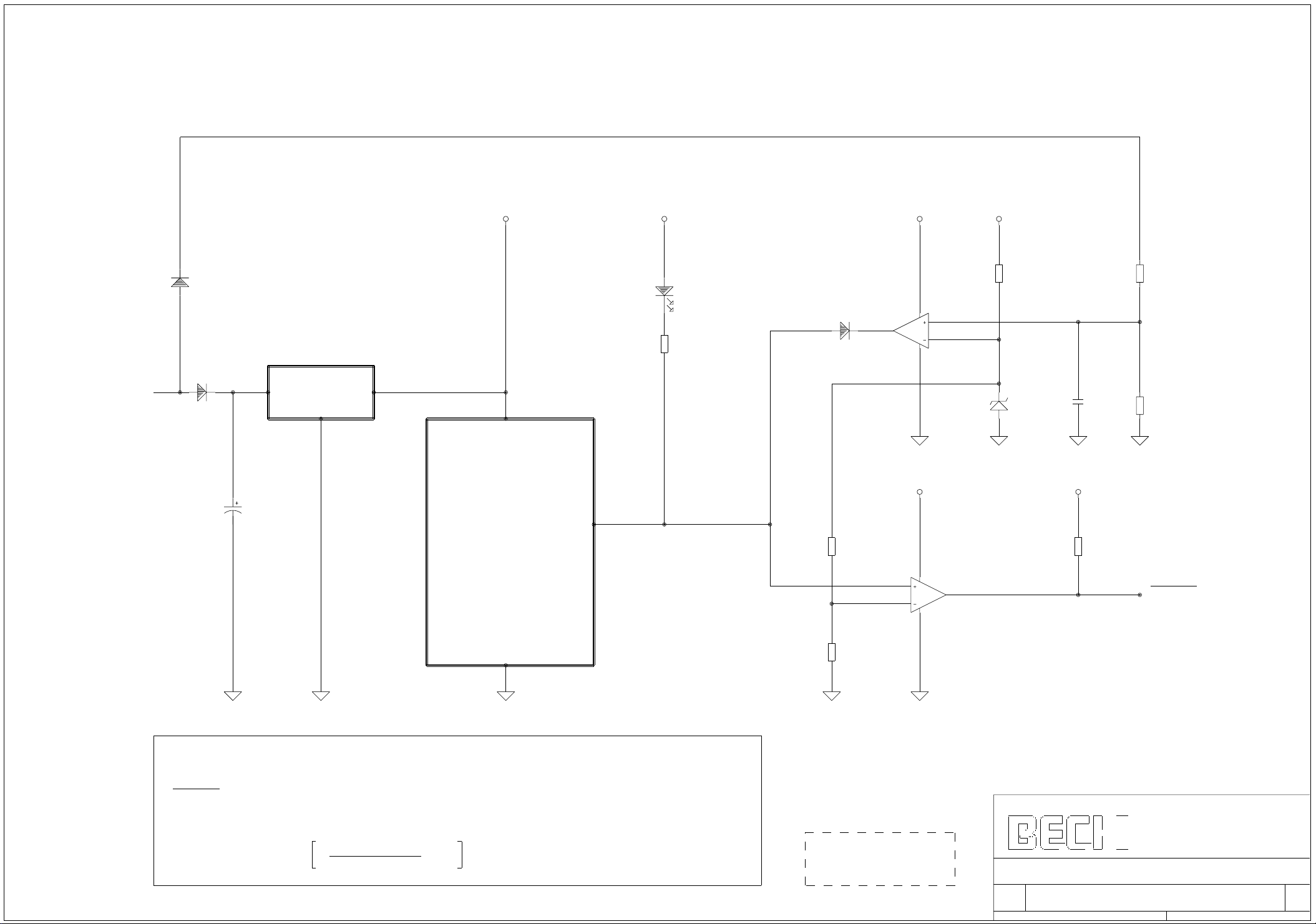
VCCVCC VCCVCC
Main
Supply
o
VPFAIL
1N4148
1N4007
DC Power supply
* CAP
5VDC
32
Vcc
@CHIP
1,2V = NMI active
0,8V = RES active
17
LINK & TRAFFIC LED
200E 1N4148
20K
1
5
6
VCC
8
4
8
4
U1A
3
2
LM393
U1B
7
LM393
1K
VREF=
2,5V
LM385 100nF 20K
VCC
1K
RES-OUT
** R1
GND
16
PFAIL = Power Fail is used to monitor main supply voltage, not main Vcc+5VDC.
This is an Analog-Comparator-Input that activates NMI.
RES-OUT = LOW active Reset Out to any external Logik.
* CAP = Value is dependent from the saveable amount of data.
** R1 = 20000 *
VPFAIL - 0,7V
2,5V
- 1
10K
Gez. : IB 16.11.99
Gepr.: JW 15.11.99
IPC GmbH
Germany - 35578 Wetzlar
Garbenheimer Strasse 38
Title
IPC@CHIP SC12 PIN17-PFAIL/RES-OUT
Size Document Number REV
A3 (C) 1995 - 1999 SC12APL1 01
Date: November 16, 1999 Sheet 1 of 1
Page 20
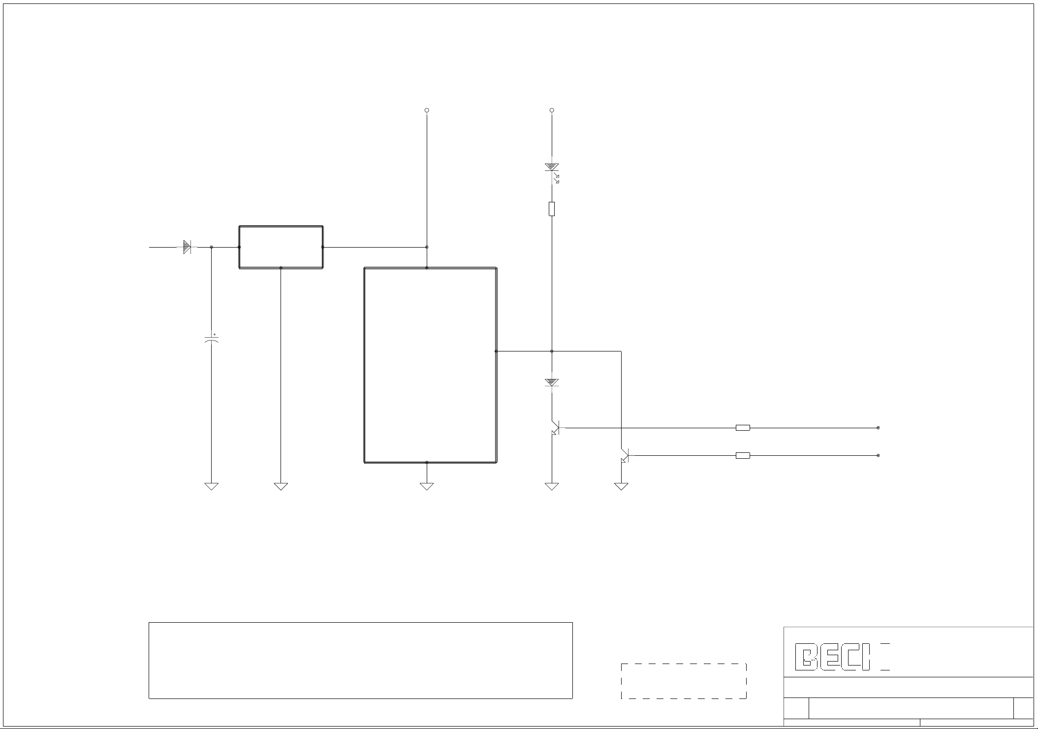
VCC
VCC
LINK & TRAFFIC LED
Main
Supply
DC Power supply
1N4007
o
5VDC
32
Vcc
200E
@CHIP
* CAP
1,2V = NMI active
0,8V = RES active
GND
16
17
1N4148
BC847
BC847
NMI-IN-EXT.
4K7
RES-IN-EXT.
4K7
NMI-IN-EXT = High active digital NMI - Input from any external Logic.
RES-IN-EXT = High active digital RES - Input from any external Logic.
* CAP = Value is dependent from the saveable amount of data. Gez. : IB 16.11.99
Gepr.: JW 15.11.99
IPC GmbH
Germany - 35578 Wetzlar
Garbenheimer Strasse 38
Title
IPC@CHIP SC12 PIN17 - NMI-IN/RES-IN
Size Document Number REV
A3 (C) 1995 - 1999 SC12APL2 01
Date: November 16, 1999 Sheet 1 of 1
Page 21
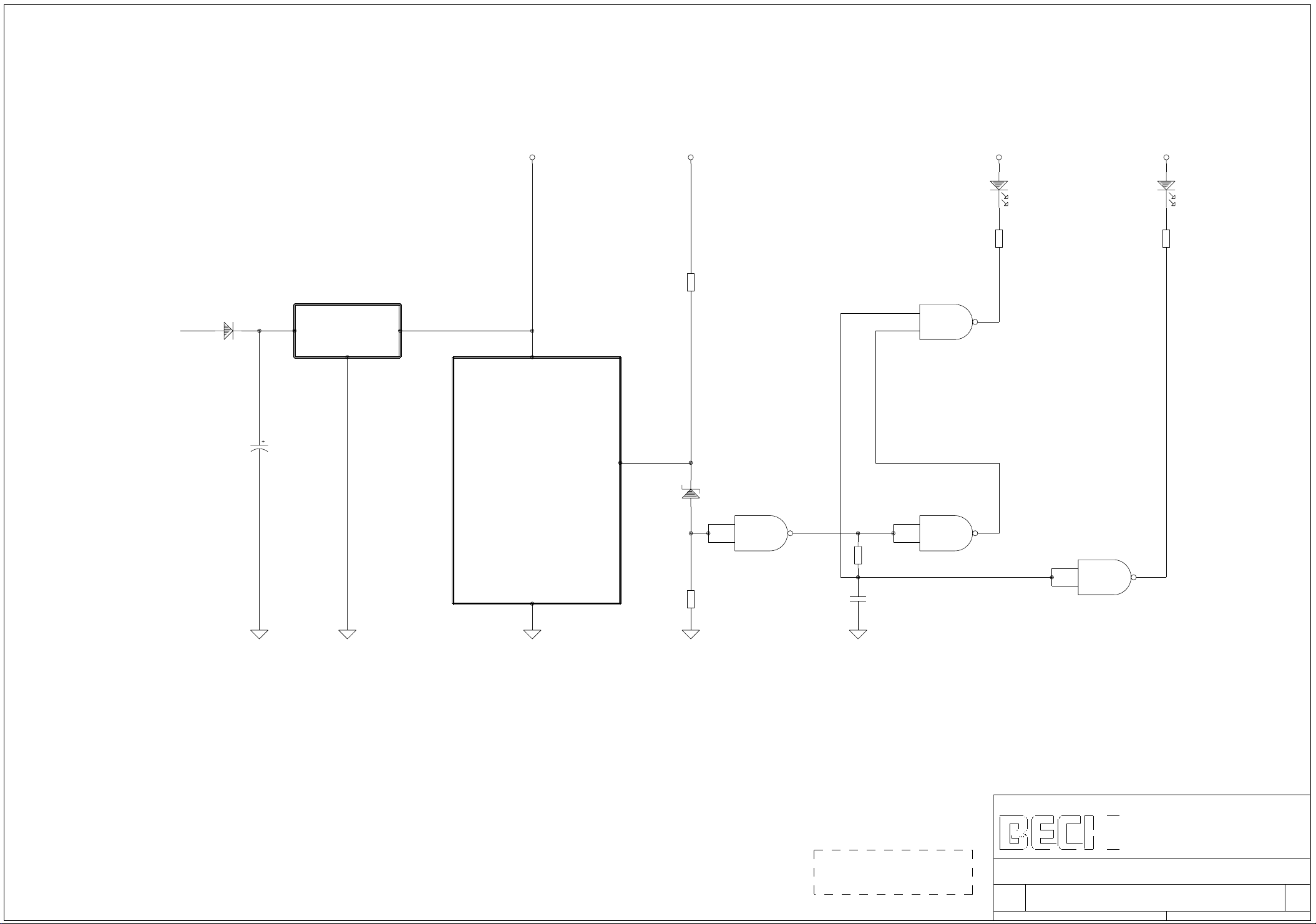
VCCVCC
VCC VCC
Traffic LED Link LED
470E 470E
Main
Supply
DC Power supply
?N400A
o
5VDC
32
Vcc
1K
9
10
U1C
8
74HCT132
@CHIP
* CAP
1,2V = NMI active
0,8V = RES active
GND
16
17
ZPD2V4
1
2
10K
U1A
74HCT132
3
100K
10uF
12
13
U1D
74HCT132
11
4
5
U1B
6
74HCT132
Gez. : IB 16.11.99
Gepr.: JW 15.11.99
IPC GmbH
Germany - 35578 Wetzlar
Garbenheimer Strasse 38
Title
IPC@CHIP SC12 PIN17-Link&Traffic LED separat
Size Document Number REV
A3 (C) 1995 - 1999 SC12APL3 01
Date: November 23, 1999 Sheet 1 of 1
Page 22

IPC GmbH
SC01/SC02/SC11/SC12
9. HOW TO CONNECT ?
The following pages contain schematics, that show different kind of ICs connected to the
IPC@CHIP family microcontroller.
Attention: These circuit examples are unevaluated! They will give you hints how to
connect different kind of ICs in different manner to the IPC@CHIP family
microcontroller.
Sc12hw09.doc page 22 of 37 24.11.1999 V0.9
TF/WB
Page 23
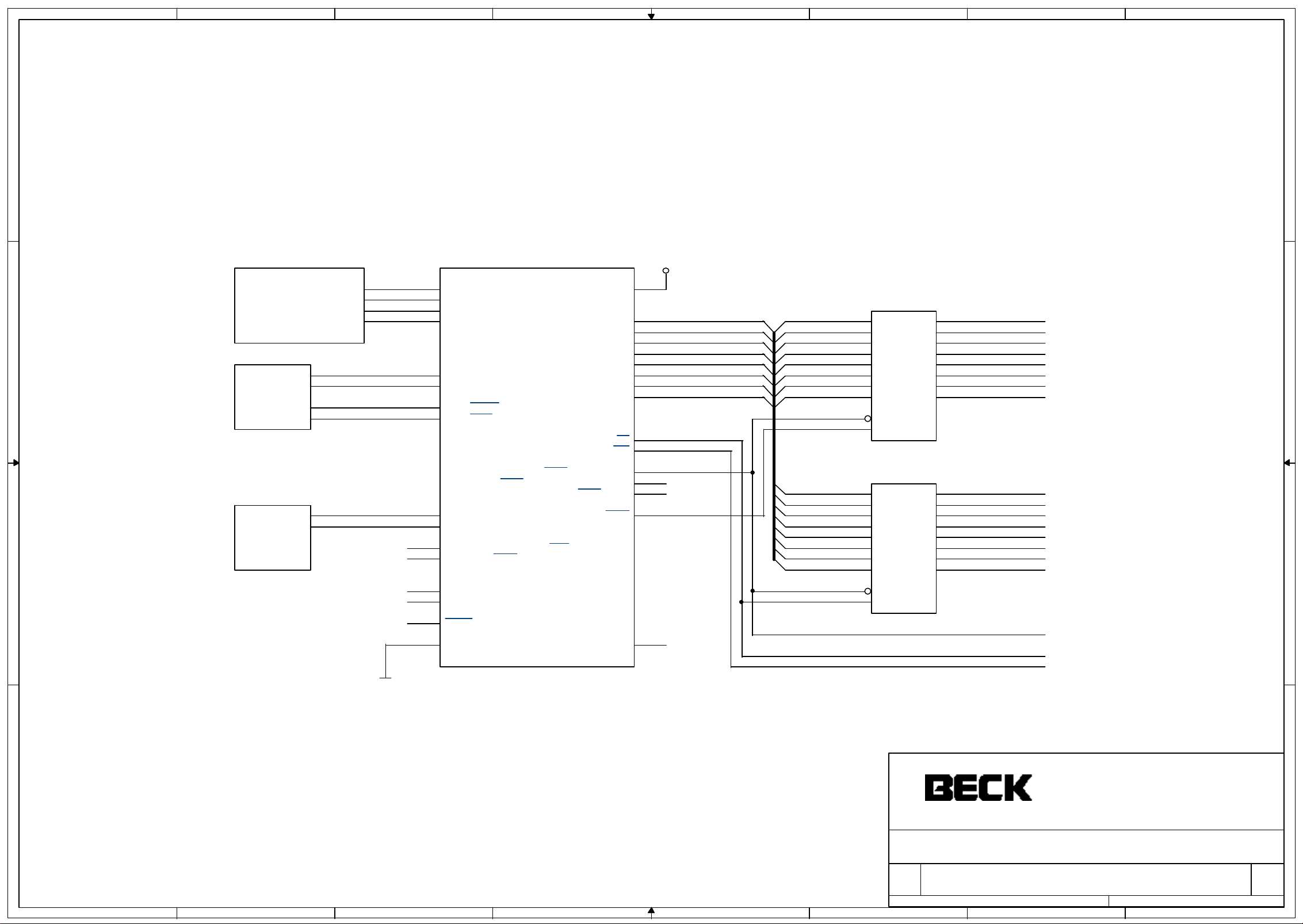
8
D D
7
6
5
4
3
2
1
256 x 8bit
I/O-Extension
IC1
IPC@CHIP SC12
VCC
18
TPTX+
19
TPTX-
20
TPRX+
21
10BaseTEXT0EXT1
C C
TPRX-
2
TXD0/P8
1
RXD0/P7
3
CTS0/ENRX0/P9
4
RTS0/RTR0/P10
MCS0/PCS1/P4/TMRIN0/A0
PCS5/P3/TMROUT1/TMRIN1/A1
PCS6/P2/A2
5
TXD1/P11
6
RXD1/INT3/P12
25
CTS1/MEN/PCS2/P6/INT2/INTA/PW
26
RTS1/MOSI/PCS3/P5/INT4
B B
31
I2CCLK/MSCK/DRQ1/INT6/P0
30
I2CDAT/MISO/DRQ0/INT5/P1
17
RESET_PFAIL_LILED
16 7
GND TMROUT0/INT0/P13
ALE/PCS0
VCC
AD0
AD1
AD2
AD3
AD4
AD5
AD6
AD7
RD
WR
32
8
9
10
11
12
13
14
15
22
23
27
28
29
24
IC2
74HCT373
AD0 AD0 A0
AD1 AD1 A1
AD2 AD2 A2
AD3 AD3 A3
AD4 AD4 A4
AD5 AD5 A5
AD6 AD6 A6
AD7 AD7 A7
PCS1#
ALE
RD#
13
14
17
18
11
3
D0
4
D1
7
D2
8
D3
D4
D5
D6
D7
1
OC
Q0
Q1
Q2
Q3
Q4
Q5
Q6
Q7
2
5
6
9
12
15
16
19
G
WR#
PCS1#
IC3
74HCT245
ALE
AD0 D0
AD1 D1
AD2 D2
AD3 D3
AD4 D4
AD5 D5
AD6 D6
AD7 D7
PCS1#
RD#
19
2
A1
3
A2
4
A3
5
A4
6
A5
7
A6
8
A7
9
A8
G
1
DIR
B1
B2
B3
B4
B5
B6
B7
B8
18
17
16
15
14
13
12
11
PCS1#
RD#
WR#
GND
IPC GmbH
A A
Germany - 35578 Wetzlar
Garbenheimer Strasse 38
Title
IPC@CHIP SC12 circuit example
Size Document Number Rev
A4
8
7
6
5
4
Date: Sheet of
3
(c) 1996 - 99 CHIPD1
2
1 1Tuesday, November 23, 1999
1
0.5
Page 24
5
4
3
2
1
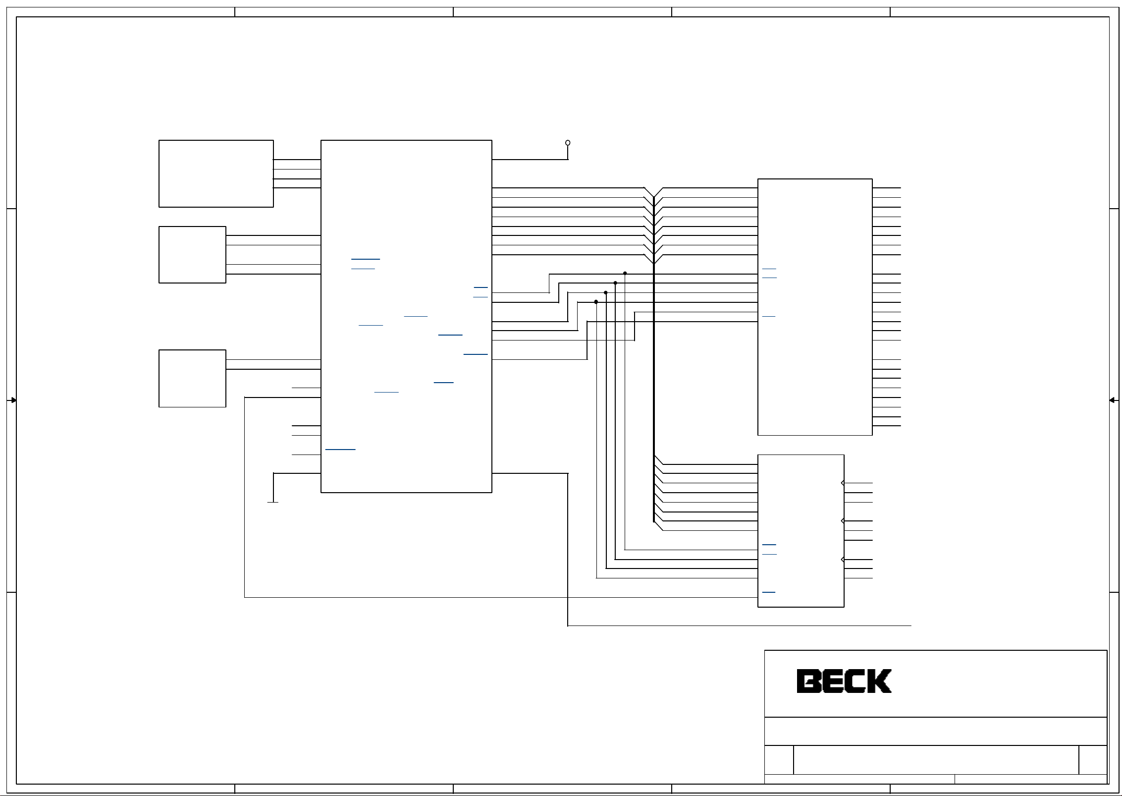
8255 24 bit I/O-Extension and
8254 Timer/Counter
D D
IC1
IPC@CHIP SC12
VCC
18
TPTX+
19
TPTX-
20
TPRX+
21
TPRX-
2
TXD0/P8
1
RXD0/P7
3
CTS0/ENRX0/P9
4
RTS0/RTR0/P10
C C
MCS0/PCS1/P4/TMRIN0/A0
PCS5/P3/TMROUT1/TMRIN1/A1
PCS6/P2/A2
5
TXD1/P11
6
RXD1/INT3/P12
EXT1 10BaseTEXT0
B B
PCS3#
25
CTS1/MEN/PCS2/P6/INT2/INTA/PW
26
RTS1/MOSI/PCS3/P5/INT4
31
I2CCLK/MSCK/DRQ1/INT6/P0
30
I2CDAT/MISO/DRQ0/INT5/P1
17
RESET_PFAIL_LILED
16 7
GND TMROUT0/INT0/P13
ALE/PCS0
GND
VCC
AD0
AD1
AD2
AD3
AD4
AD5
AD6
AD7
RD
WR
32
8
AD0
AD1
9
AD2
10
AD3 AD3
11
AD4
12
13
AD5
AD6
14
AD7
15
RD#
22
WR#
23
A0
27
28
A1
Res et
29
PCS0#
24
TMROUT1
AD0
AD1
AD2
AD4
AD5
AD6
AD7
RD#
WR#
A0
A1
Reset
PCS0#
AD0
AD1
AD2
AD3
AD4
AD5
AD6
AD7
RD#
WR#
A0
A1
PCS3#
34
33
32
31
30
29
28
27
36
35
22
23
19
20
21
5
9
8
6
8
7
6
5
4
3
2
1
IC2
D0
D1
D2
D3
D4
D5
D6
D7
RD
WR
A0
A1
RESET
CS
8255
IC3
D0
D1
D2
D3
D4
D5
D6
D7
RD
WR
A0
A1
CS
CLK0
G0
OUT0
CLK1
G1
OUT1
CLK2
G2
OUT2
PA0
PA1
PA2
PA3
PA4
PA5
PA6
PA7
PB0
PB1
PB2
PB3
PB4
PB5
PB6
PB7
PC0
PC1
PC2
PC3
PC4
PC5
PC6
PC7
9
11
10
15
14
13
18
16
17
4
3
2
1
40
39
38
37
18
19
20
21
22
23
24
25
14
15
16
17
13
12
11
10
8254
IPC GmbH
A A
Germany - 35578 Wetzlar
Garbenheimer Stra sse 38
Title
IPC@CHIP SC12 circuit example
Size Document Num ber Rev
A4
5
4
3
Date: Sheet of
2
(c) 1996 - 99 CHIP D1
1 1Tuesday, November 23, 1999
1
0.5
Page 25
5
D D
4
3
2
1
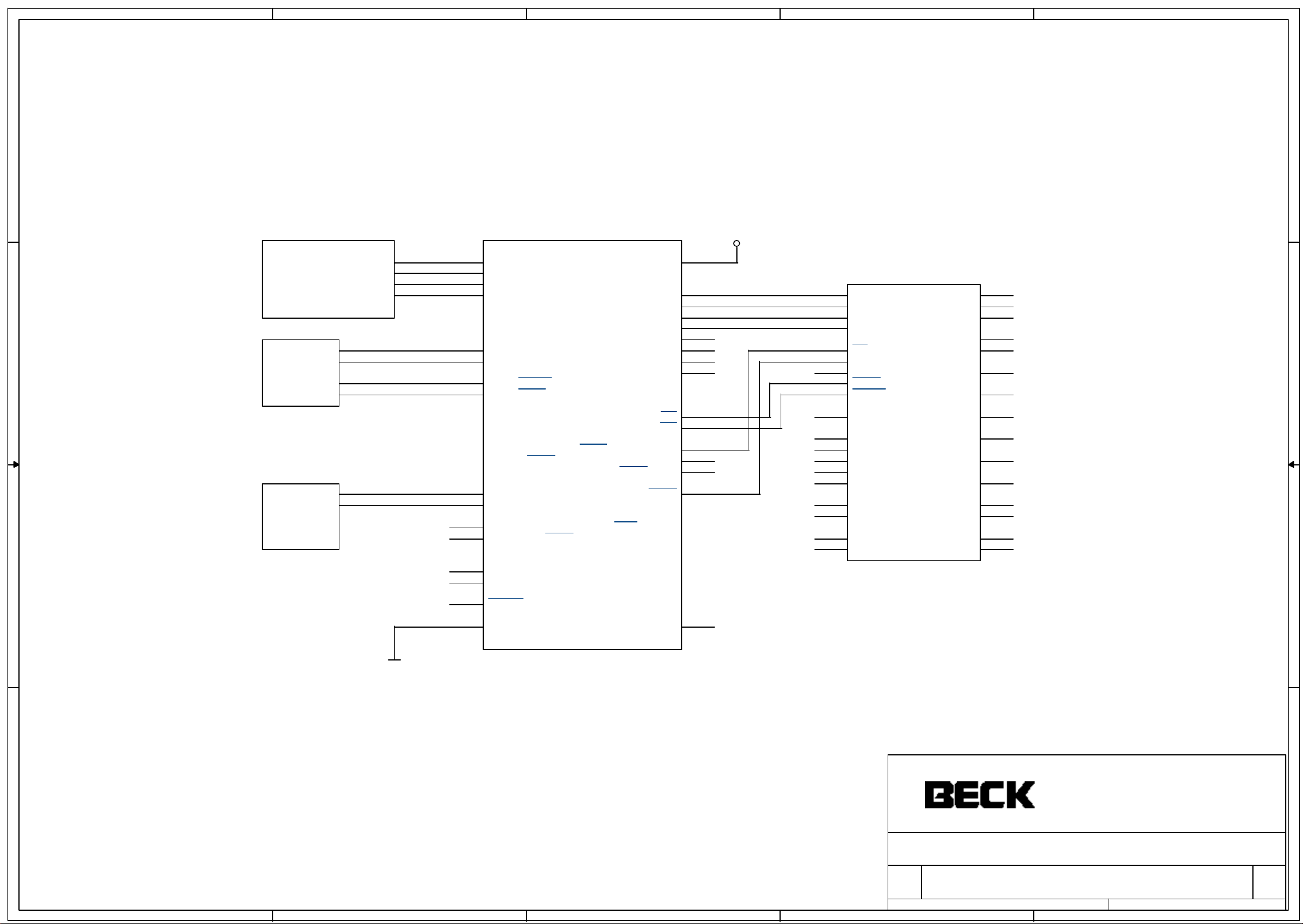
Multimeter ADC MAX133CPL
IC1
IPC@CHIP SC12
VCC
18
TPTX+
19
TPTX-
20
TPRX+
21
TPRX-
2
C C
TXD0/P8
1
RXD0/P7
3
CTS0/ENRX0/P9
4
RTS0/RTR0/P10
MCS0/PCS1/P4/TMRIN0/A0
PCS5/P3/TMROUT1/TMRIN1/A1
PCS6/P2/A2
5
TXD1/P11
6
RXD1/INT3/P12
EXT1 10BaseTEXT0
B B
25
CTS1/MEN/PCS2/P6/INT2/INTA/PW
26
RTS1/MOSI/PCS3/P5/INT4
31
I2CCLK/MSCK/DRQ1/INT6/P0
30
I2CDAT/MISO/DRQ0/INT5/P1
17
RESET_PFAIL_LILED
16 7
GND TMROUT0/INT0/P13
ALE/PCS0
VCC
AD0
AD1
AD2
AD3
AD4
AD5
AD6
AD7
RD
WR
32
8
9
10
11
12
13
14
15
22
23
27
28
29
24
AD0
AD1
AD2
AD3
RD#
WR#
ALE
39
38
37
36
3
4
5
40
1
11
16
17
18
19
20
27
33
7
8
IC2
AD0
AD1
AD2
AD3
CS
ALE
BCO
READ
WRITE
IN LO
10M
1.11M
101K
10K
1K
400MV
CURRENT
OSC1
OSC2
MAX133CP L
OHMS
COMMON
VREF
EOC
BEEP
FRI
FRO
FAI
FAO
EAI
EAO
INT IN
INT OUT
BUFF 1
BUFF 2
32
22
26
9
10
31
23
14
15
29
28
13
12
34
35
GND
IPC GmbH
A A
Germany - 35578 Wetzlar
Garbenheimer Stra sse 38
Title
IPC@CHIP SC12 circuit example
Size Document Num ber Rev
A4
5
4
3
Date: Sheet of
2
(c) 1996 - 99 CHIPD1
1 1Tuesday, November 23, 1999
1
0.5
Page 26
5
4
3
2
1
D D
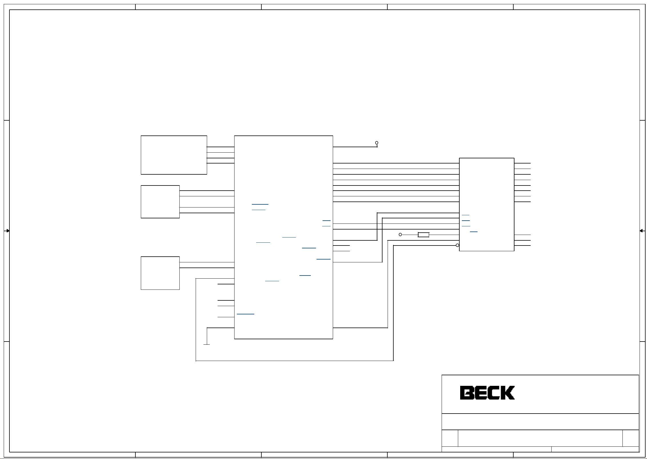
8259 peripheral interrupt controller
IC1
IPC@CHIP SC12
18
TPTX+
19
TPTX-
20
TPRX+
21
TPRX-
C C
2
TXD0/P8
1
RXD0/P7
3
CTS0/ENRX0/P9
4
RTS0/RTR0/P10
MCS0/PCS1/P4/TMRIN0/A0
PCS5/P3/TMROUT1/TMRIN1/A1
PCS6/P2/A2
5
TXD1/P11
6
RXD1/INT3/P12
EXT1 10BaseTEXT0
B B
INTA#
25
CTS1/MEN/PCS2/P6/INT2/INTA/PW
26
RTS1/MOSI/PCS3/P5/INT4
ALE/PCS0
VCC
AD0
AD1
AD2
AD3
AD4
AD5
AD6
AD7
RD
WR
32
8
9
10
11
12
13
14
15
22
23
27
28
29
24
AD0
AD1
AD2
AD3
AD4
AD5
AD6
AD7
RD#
WR#
A0
PCS0#
VCC
VCC
R1 1K
11
10
27
16
17
26
9
8
7
6
5
4
1
3
2
IC2
8259A
D0
D1
D2
D3
D4
D5
D6
D7
A0
CS
RD
WR
SP/EN
INT
INTA
IR0
IR1
IR2
IR3
IR4
IR5
IR6
IR7
CAS0
CAS1
CAS2
18
19
20
21
22
23
24
25
12
13
15
31
I2CCLK/MSCK/DRQ1/INT6/P0
30
I2CDAT/MISO/DRQ0/INT5/P1
17
RESET_PFAIL_LILED
16 7
GND TMROUT0/INT0/P13
INT0
GND
IPC GmbH
A A
Germany - 35578 Wetzlar
Garbenheimer Str asse 38
Title
IPC@CHIP SC12 circuit example
Size Document Num ber Re v
A4
5
4
3
Date: Sheet of
2
(c) 1996 - 99 CHIP D1
1 1Tuesday, November 23, 1999
1
0.5
Page 27
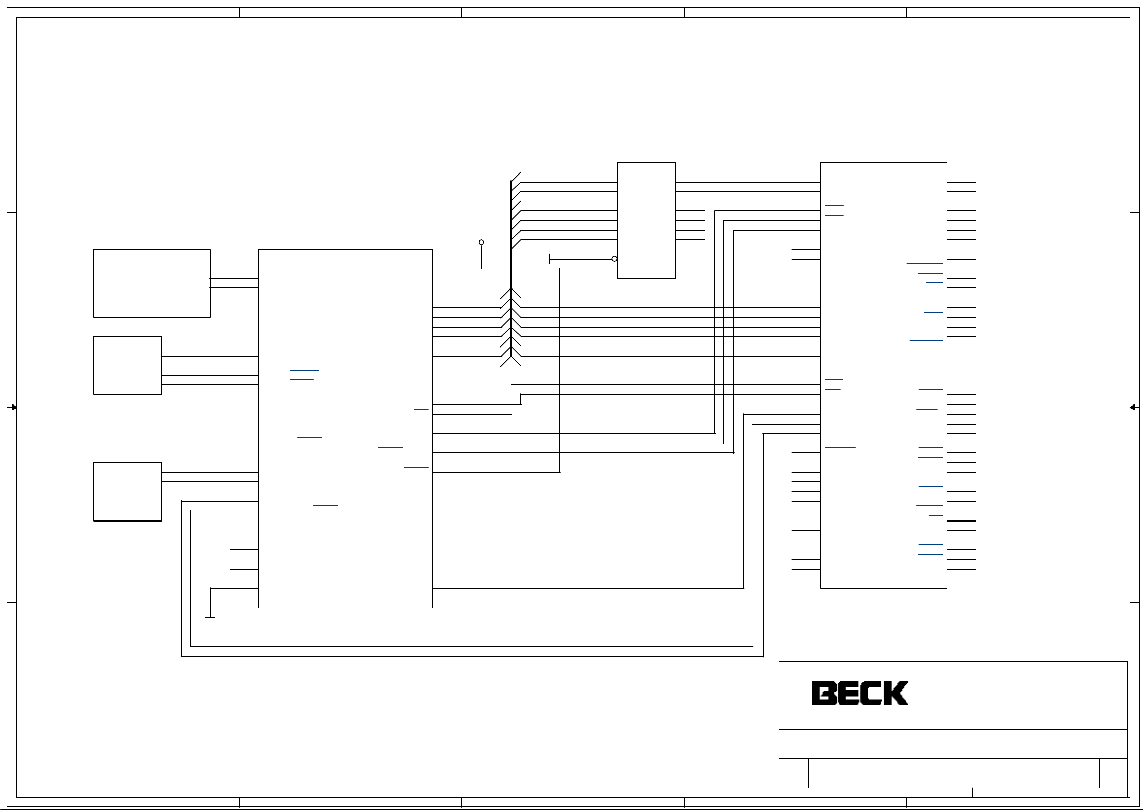
5
4
3
2
1
16C452/552 2 UART with FIFO
D D
IC1
IPC@CHIP SC12
18
TPTX+
19
TPTX-
20
TPRX+
21
TPRX-
C C
2
TXD0/P8
1
RXD0/P7
3
CTS0/ENRX0/P9
4
RTS0/RTR0/P10
5
TXD1/P11
6
RXD1/INT3/P12
B B
EXT1 10BaseTEXT0
INT2
INT4
25
CTS1/MEN/PCS2/P6/INT2/INTA/PW
26
RTS1/MOSI/PCS3/P5/INT4
31
I2CCLK/MSCK/DRQ1/INT6/P0
30
I2CDAT/MISO/DRQ0/INT5/P1
17
RESET_PFAIL_LILED
16 7
GND TMROUT0/INT0/P13
and Printer Port
VCC
32
VCC
AD0
8
AD0
AD1
AD2
AD3
AD4
AD5
AD6
AD7
RD
WR
MCS0/PCS1/P4/TMRIN0/A0
PCS5/P3/TMROUT1/TMRIN1/A1
PCS6/P2/A2
ALE/PCS0
9
10
11
12
13
14
15
22
23
27
28
29
24
AD1
AD2
AD3
AD4
AD5
AD6
AD7
RD#
WR#
PCS1#
PCS5#
PCS6#
ALE
INT0
AD0
AD1
AD2
AD3
AD4
AD5
AD6
AD7
GND
AD0
AD1
AD2
AD3
AD4
AD5
AD6
AD7
ALE
IC3
74HCT373
3
4
7
8
13
14
17
18
1
11
D0
D1
D2
D3
D4
D5
D6
D7
OC
G
Q0
Q1
Q2
Q3
Q4
Q5
Q6
Q7
2
5
6
9
12
15
16
19
A0
A1
A2
INT0
INT4
INT2
35
34
33
32
3
38
44
2
14
15
16
17
18
19
20
21
36
37
45
60
59
39
9
61
22
42
4
43
1
IC2
A0
A1
A2
CS0
CS1
CS2
BD0
TRI
D0
D1
D2
D3
D4
D5
D6
D7
IOW
IOR
INT0
INT1
INT2
RESET
RXRDY0#
RXRDY1#
TXRDY0#
TXRDY1#
CLK
ENIRQ
LPTOE
16C452/552
P0
P1
P2
P3
P4
P5
P6
P7
STROB
AUTOFD
SLCT
INIT
BUSY
ACK
PE
SLCT
ERROR
CTS1
DSR1
DCD1
RI1
SIN1
RTS1
DTR1
SOUT1
CTS2
DSR2
DCD2
RI2
SIN2
RTS2
DTR2
SOUT2
53
52
51
50
49
48
47
46
55
56
58
57
66
68
67
65
63
28
31
29
30
41
24
25
26
13
5
8
6
62
12
11
10
GND
IPC GmbH
A A
Germany - 35578 Wetzlar
Garbenheimer Stra sse 38
Title
IPC@CHIP SC12 circuit example
Size Document Num ber Rev
A4
5
4
3
Date: Sheet of
2
(c) 1996 - 99 CHIP D1
1 1Tuesday, November 23, 1999
1
0.5
Page 28
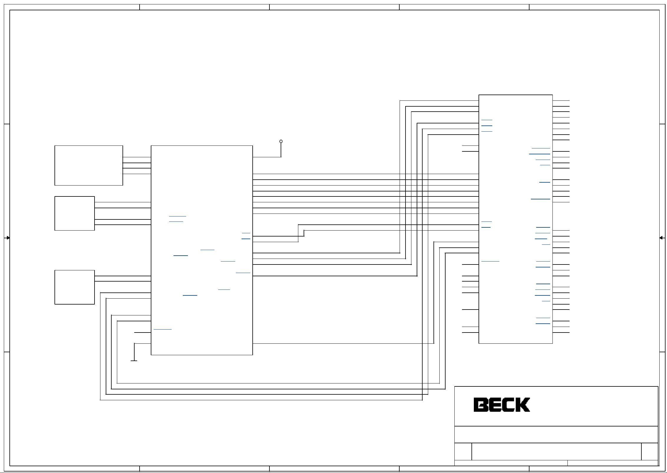
5
4
3
2
1
16C452/552 2 UART with FIFO
D D
and Printer Port
A0
A1
A2
PCS0#
PCS2#
IC1
IPC@CHIP SC12
18
TPTX+
19
TPTX-
20
TPRX+
21
TPRX-
C C
2
TXD0/P8
1
RXD0/P7
3
CTS0/ENRX0/P9
4
RTS0/RTR0/P10
MCS0/PCS1/P4/TMRIN0/A0
PCS5/P3/TMROUT1/TMRIN1/A1
PCS6/P2/A2
5
TXD1/P11
6
RXD1/INT3/P12
B B
EXT1 10BaseTEXT0
PCS2#
PCS3#
INT6
INT5
25
CTS1/MEN/PCS2/P6/INT2/INTA/PW
26
RTS1/MOSI/PCS3/P5/INT4
31
I2CCLK/MSCK/DRQ1/INT6/P0
30
I2CDAT/MISO/DRQ0/INT5/P1
17
RESET_PFAIL_LILED
16 7
GND TMROUT0/INT0/P13
ALE/PCS0
VCC
AD0
AD1
AD2
AD3
AD4
AD5
AD6
AD7
RD
WR
32
8
9
10
11
12
13
14
15
22
23
27
28
29
24
VCC
AD0
AD1
AD2
AD3
AD4
AD5
AD6
AD7
RD#
WR#
A0
A1
A2
PCS0#
INT0
PCS3#
INT0
INT5
INT6
35
34
33
32
3
38
44
2
14
15
16
17
18
19
20
21
36
37
45
60
59
39
9
61
22
42
4
43
1
A0
A1
A2
CS0
CS1
CS2
BD0
TRI
D0
D1
D2
D3
D4
D5
D6
D7
IOW
IOR
INT0
INT1
INT2
RESET
RXRDY0#
RXRDY1#
TXRDY0#
TXRDY1#
CLK
ENIRQ
LPTOE
16C452/552
P0
P1
P2
P3
P4
P5
P6
P7
STROB
AUTOFD
SLCT
INIT
BUSY
ACK
PE
SLCT
ERROR
CTS1
DSR1
DCD1
RI1
SIN1
RTS1
DTR1
SOUT1
CTS2
DSR2
DCD2
RI2
SIN2
RTS2
DTR2
SOUT2
53
52
51
50
49
48
47
46
55
56
58
57
66
68
67
65
63
28
31
29
30
41
24
25
26
13
5
8
6
62
12
11
10
IC2
GND
IPC GmbH
A A
Germany - 35578 Wetzlar
Garbenheimer Stra sse 38
Title
IPC@CHIP SC12 circuit example
Size Document Num ber Rev
A4
5
4
3
Date: Sheet of
2
(c) 1996 - 99 CHIP D1
1 1Tuesday, November 23, 1999
1
0.5
Page 29
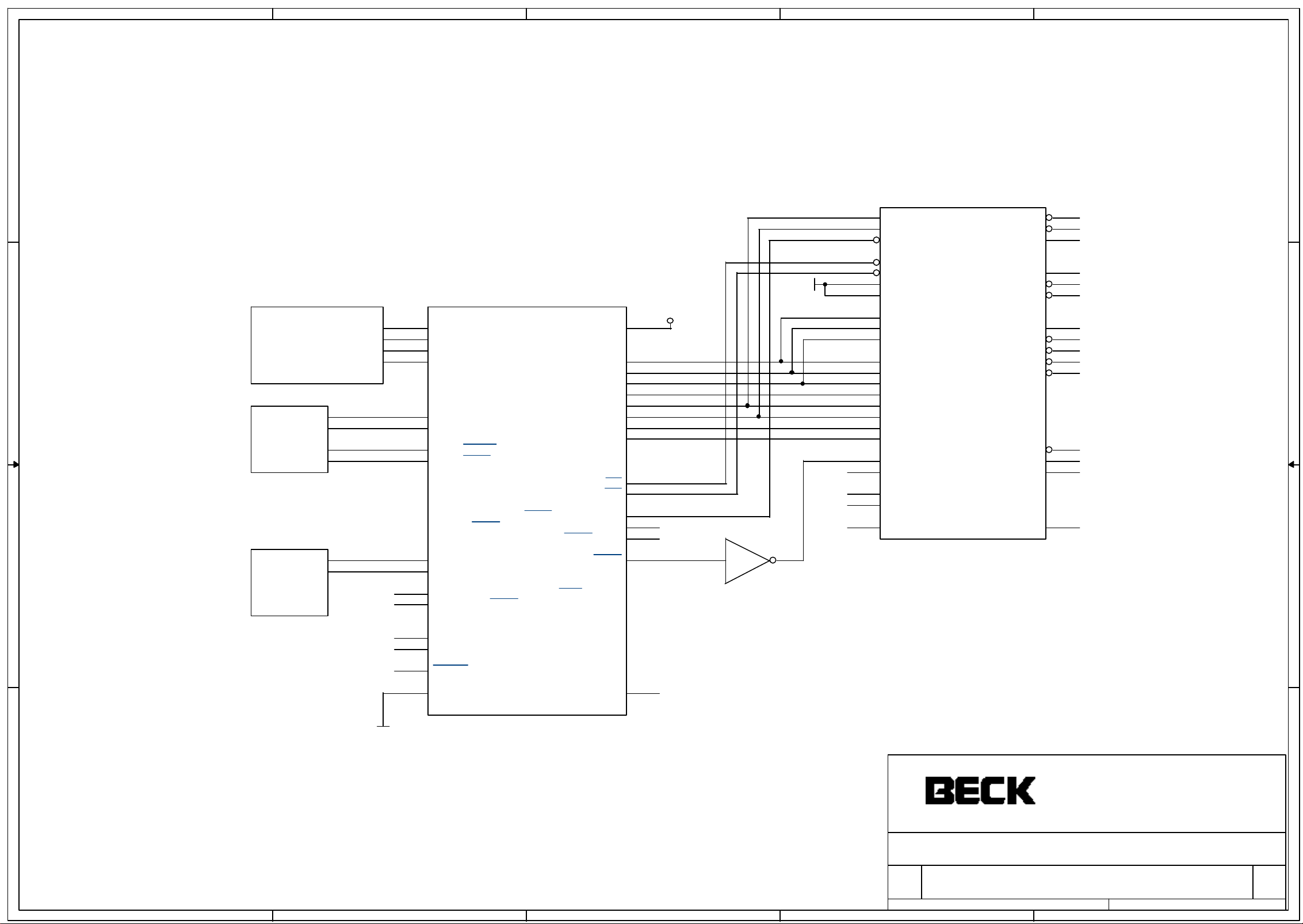
5
D D
4
3
2
1
UART 8250 with
multiplexed
address/data bus
IC1
IPC@CHIP SC12
18
TPTX+
19
TPTX-
20
C C
B B
EXT1 10BaseTEXT0
TPRX+
21
TPRX-
2
TXD0/P8
1
RXD0/P7
3
CTS0/ENRX0/P9
4
RTS0/RTR0/P10
MCS0/PCS1/P4/TMRIN0/A0
PCS5/P3/TMROUT1/TMRIN1/A1
5
TXD1/P11
6
RXD1/INT3/P12
25
CTS1/MEN/PCS2/P6/INT2/INTA/PW
26
RTS1/MOSI/PCS3/P5/INT4
PCS6/P2/A2
VCC
AD0
AD1
AD2
AD3
AD4
AD5
AD6
AD7
RD
WR
ALE/PCS0
32
8
9
10
11
12
13
14
15
22
23
27
28
29
24
VCC
AD0
AD1
AD2
AD3
AD4
AD5
AD6
AD7
RD#
WR#
PCS1#
IC3A
1 2
74HCT04
GND
12
13
14
21
18
22
19
28
27
26
1
2
3
4
5
6
7
8
25
35
16
17
9
IC2
CS0
CS1
CS2
RD
WR
RD
WR
A0
A1
A2
D0
D1
D2
D3
D4
D5
D6
D7
ADS
RESET
XTAL1/CLK
XTAL2
RCLK
8250
OUT1
OUT2
INT
TXD
RTS
DTR
RXD
DCD
DSR
CTS
CSOUT
DDIS
NC
BAUDOUT
RI
34
31
30
11
32
33
10
38
37
36
39
24
23
29
15
31
I2CCLK/MSCK/DRQ1/INT6/P0
30
I2CDAT/MISO/DRQ0/INT5/P1
17
RESET_PFAIL_LILED
16 7
GND TMROUT0/INT0/P13
GND
IPC GmbH
A A
Title
Germany - 35578 Wetzlar
Garbenheimer Stra sse 38
IPC@CHIP SC12 circuit example
Size Document Num ber Rev
A4
5
4
3
Date: Sheet of
2
(c) 1996 - 99 CHIP D1
1 1Tuesday, November 23, 1999
1
0.5
Page 30
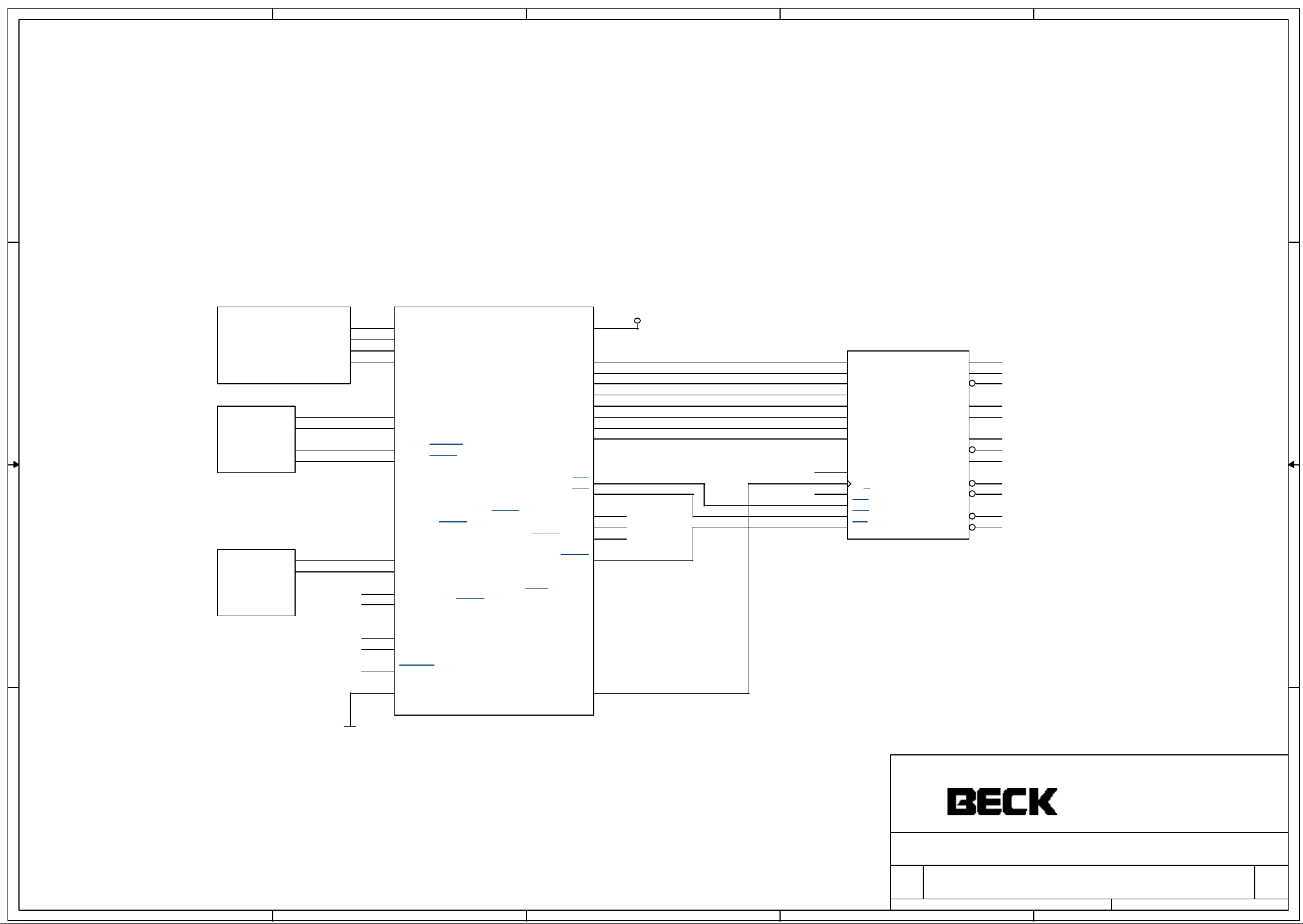
5
D D
4
3
2
1
UART 8251
IC1
IPC@CHIP SC12
18
TPTX+
19
TPTX-
20
C C
TPRX+
21
TPRX-
2
TXD0/P8
1
RXD0/P7
3
CTS0/ENRX0/P9
4
RTS0/RTR0/P10
MCS0/PCS1/P4/TMRIN0/A0
PCS5/P3/TMROUT1/TMRIN1/A1
PCS6/P2/A2
5
TXD1/P11
6
B B
EXT1 10BaseTEXT0
RXD1/INT3/P12
25
CTS1/MEN/PCS2/P6/INT2/INTA/PW
26
RTS1/MOSI/PCS3/P5/INT4
31
I2CCLK/MSCK/DRQ1/INT6/P0
30
I2CDAT/MISO/DRQ0/INT5/P1
17
RESET_PFAIL_LILED
16 7
GND TMROUT0/INT0/P13
ALE/PCS0
VCC
AD0
AD1
AD2
AD3
AD4
AD5
AD6
AD7
RD
WR
32
8
9
10
11
12
13
14
15
22
23
27
28
29
24
AD0
AD1
AD2
AD3
AD4
AD5
AD6
AD7
RD#
WR#
27
28
21
20
12
13
10
11
1
2
5
6
7
8
IC2
D0
D1
D2
D3
D4
D5
D6
D7
RESET
CLK
C/D
RD
WR
CS
8251
TXRDY
TXE
TXC
TXD
RXD
RXRDY
RXC
SY/BR
DSR
DTR
CTS
RTS
15
18
9
19
3
14
25
16
22
24
17
23
VCC
GND
IPC GmbH
A A
Germany - 35578 Wetzlar
Garbenheimer Stra sse 38
Title
IPC@CHIP SC12 circuit example
Size Document Numb er Rev
A4
5
4
3
Date: Sheet of
2
(c) 1996 - 99 CHIP D1
1 1Tuesday, November 23, 1999
1
0.5
Page 31
5
D D
4
3
2
1
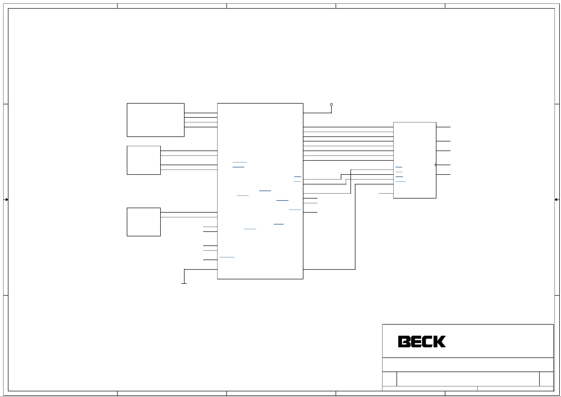
low-cost 8bit ADC
IC1
IPC@CHIP SC12
VCC
18
TPTX+
19
TPTX-
20
TPRX+
21
10BaseTEXT0EXT1
C C
TPRX-
2
TXD0/P8
1
RXD0/P7
3
CTS0/ENRX0/P9
4
RTS0/RTR0/P10
VCC
MCS0/PCS1/P4/TMRIN0/A0
PCS5/P3/TMROUT1/TMRIN1/A1
PCS6/P2/A2
5
TXD1/P11
6
RXD1/INT3/P12
25
CTS1/MEN/PCS2/P6/INT2/INTA/PW
26
RTS1/MOSI/PCS3/P5/INT4
31
I2CCLK/MSCK/DRQ1/INT6/P0
B B
30
I2CDAT/MISO/DRQ0/INT5/P1
17
RESET_PFAIL_LILED
16 7
GND TMROUT0/INT0/P13
ALE/PCS0
AD0
AD1
AD2
AD3
AD4
AD5
AD6
AD7
RD
WR
32
8
9
10
11
12
13
14
15
22
23
27
28
29
24
AD0
AD1
AD2
AD3
AD4
AD5
AD6
AD7
RD#
WR#
PCS1#
INT0
18
17
16
15
14
13
12
11
1
2
3
5
8
IC2
DB0
DB1
DB2
DB3
DB4
DB5
DB6
DB7
CS
RD
WR
INTR
AGND
ADC0804
VI+
VI-
CLKR
CLK
VREF
6
7
19
4
9
GND
IPC GmbH
A A
Germany - 35578 Wetzlar
Garbenheimer Stra sse 38
Title
IPC@CHIP SC12 circuit example
Size Document Num ber Rev
A4
5
4
3
Date: Sheet of
2
(c) 1996 - 99 CHIPD1
1 1Tuesday, November 23, 1999
1
0.5
Page 32
5
4
3
2
1
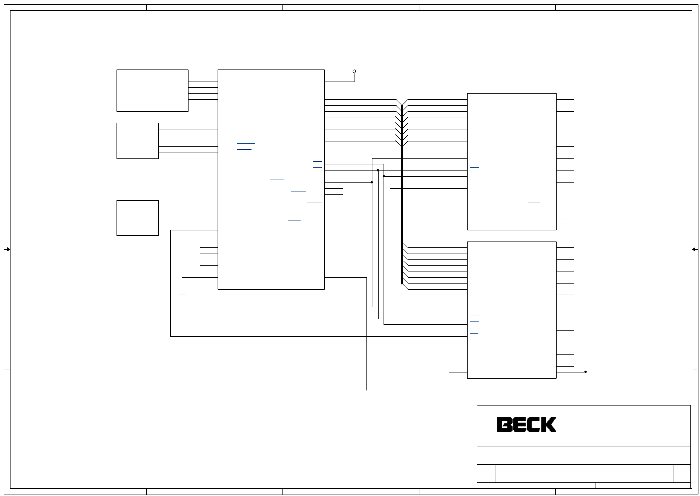
16x 10bit ADC with 2x µPD7004
IC1
IPC@CHIP SC12
D D
18
TPTX+
19
TPTX-
20
TPRX+
21
TPRX-
2
TXD0/P8
1
RXD0/P7
3
CTS0/ENRX0/P9
4
RTS0/RTR0/P10
VCC
MCS0/PCS1/P4/TMRIN0/A0
C C
5
TXD1/P11
6
RXD1/INT3/P12
EXT1 10BaseTEXT0
PCS3#
25
CTS1/MEN/PCS2/P6/INT2/INTA/PW
26
RTS1/MOSI/PCS3/P5/INT4
31
I2CCLK/MSCK/DRQ1/INT6/P0
30
I2CDAT/MISO/DRQ0/INT5/P1
17
RESET_PFAIL_LILED
16 7
GND TMROUT0/INT0/P13
PCS5/P3/TMROUT1/TMRIN1/A1
PCS6/P2/A2
ALE/PCS0
AD0
AD1
AD2
AD3
AD4
AD5
AD6
AD7
RD
WR
32
8
9
10
11
12
13
14
15
22
23
27
28
29
24
GND
B B
VCC
AD0
AD1
AD2
AD3
AD4
AD5
AD6
AD7
RD#
WR#
A0
PCS0#
TMROUT0
AD0
AD1
AD2
AD3
AD4
AD5
AD6
AD7
A0
WR#
RD#
PCS0#
AD0
AD1
AD2
AD3
AD4
AD5
AD6
AD7
A0
WR#
RD#
PCS3#
14
13
12
11
10
9
8
7
20
19
21
22
5
14
13
12
11
10
9
8
7
20
19
21
22
IC2
DB0
DB1
DB2
DB3
DB4
DB5
DB6
DB7
A0
WR
RD
CS
V REF
UPD70 04
IC3
DB0
DB1
DB2
DB3
DB4
DB5
DB6
DB7
A0
WR
RD
CS
ACH0
ACH1
ACH2
ACH3
ACH4
ACH5
ACH6
ACH7
EOC OUT
MODE
CLKIN
ACH0
ACH1
ACH2
ACH3
ACH4
ACH5
ACH6
ACH7
25
26
27
28
1
2
3
4
16
18
17
25
26
27
28
1
2
3
4
EOC OUT
5
V REF
MODE
CLKIN
16
18
17
UPD70 04
IPC GmbH
A A
Germany - 35578 Wetzlar
Garbenheimer Stra sse 38
Title
IPC@CHIP SC12 circuit example
Size Document Num ber Rev
A4
5
4
3
Date: Sheet of
2
(c) 1996 - 99 CHIP D1
1 1Tuesday, November 23, 1999
1
0.5
Page 33
5
4
3
2
1
D D
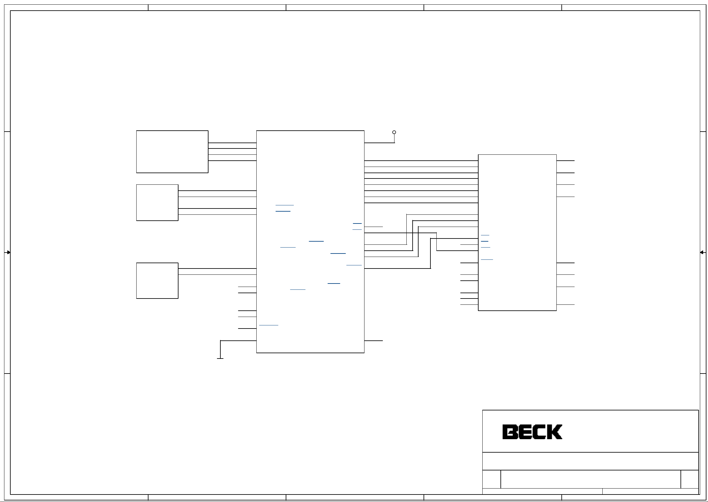
DAC4815 4x 12bit
IC1
IPC@CHIP SC12
18
TPTX+
19
TPTX-
20
TPRX+
21
TPRX-
2
C C
TXD0/P8
1
RXD0/P7
3
CTS0/ENRX0/P9
4
RTS0/RTR0/P10
MCS0/PCS1/P4/TMRIN0/A0
PCS5/P3/TMROUT1/TMRIN1/A1
PCS6/P2/A2
5
TXD1/P11
6
RXD1/INT3/P12
EXT1 10BaseTEXT0
B B
25
CTS1/MEN/PCS2/P6/INT2/INTA/PW
26
RTS1/MOSI/PCS3/P5/INT4
31
I2CCLK/MSCK/DRQ1/INT6/P0
30
I2CDAT/MISO/DRQ0/INT5/P1
17
RESET_PFAIL_LILED
16 7
GND TMROUT0/INT0/P13
ALE/PCS0
VCC
AD0
AD1
AD2
AD3
AD4
AD5
AD6
AD7
RD
WR
32
8
9
10
11
12
13
14
15
22
23
27
28
29
24
VCC
AD0
AD1
AD2
AD3
AD4
AD5
AD6
AD7
WR#
A0
A1
A2
PCS0#
18
19
20
21
22
23
24
25
26
27
28
16
17
15
14
11
10
8
9
7
IC?
D0
D1
D2
D3
D4
D5
D6
D7
A0
A1
A2
CS
LE
WR
CLR
+5V
DGND
+15V
AGND
-15V
DAC4815
VOUTA
VOUTB
VOUTC
VOUTD
-REFOUT
-REFIN
+REFOUT
BPO
2
1
13
12
3
4
5
6
GND
IPC GmbH
A A
Germany - 35578 Wetzlar
Garbenheimer Stra sse 38
Title
IPC@CHIP SC12 circuit example
Size Document Num ber Rev
A4
5
4
3
Date: Sheet of
2
(c) 1996 - 99 CHIP D1
1 5Tuesday, November 23, 1999
1
0.5
Page 34
5
4
3
2
1
D D
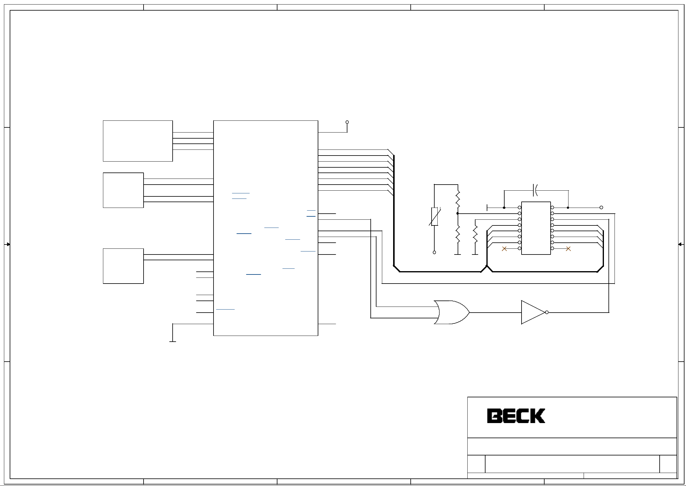
LC-Display
IC1
IPC@CHIP SC12
VCC
18
TPTX+
19
TPTX-
20
TPRX+
21
10BaseTEXT0
C C
TPRX-
2
TXD0/P8
1
RXD0/P7
3
CTS0/ENRX0/P9
4
RTS0/RTR0/P10
VCC
MCS0/PCS1/P4/TMRIN0/A0
PCS5/P3/TMROUT1/TMRIN1/A1
PCS6/P2/A2
EXT1
5
TXD1/P11
6
RXD1/INT3/P12
25
CTS1/MEN/PCS2/P6/INT2/INTA/PW
26
RTS1/MOSI/PCS3/P5/INT4
ALE/PCS0
AD0
AD1
AD2
AD3
AD4
AD5
AD6
AD7
RD
WR
32
8
9
10
11
12
13
14
15
22
23
27
28
29
24
AD0
AD1
AD2
AD3
AD4
AD5
AD6
AD7
WR#
A0
PCS5#
TS2
NTC10K
12
VCC
R17
1k6
GND GND
DISPLAY 20x2
C10
R16
6k
GND VCC
0V +5V
V0
ST14
R_W PCS5_WR
D0 D1
D2
R82
1k
A_LED K_LED
MICRO-MATCH16
100nF
12
34
56
78
910
1112
1314
1516
RSEL
D3
D5D4
D7D6
31
I2CCLK/MSCK/DRQ1/INT6/P0
30
B B
I2CDAT/MISO/DRQ0/INT5/P1
17
RESET_PFAIL_LILED
16 7
GND TMROUT0/INT0/P13
PCS5#
WR#
13
11
12
74HCT32
IC20D
IC13F
13 12
74HCT1 4
SO14S
GND
IPC GmbH
A A
Germany - 35578 Wetzlar
Garbenheimer Stra sse 38
Title
IPC@CHIP SC12 Beschaltungsbeispiel
Size Document Num ber Rev
A4
5
4
3
Date: Sheet of
2
(c) 1996 - 99 CHIP D1
1 1Tuesday, November 23, 1999
1
0.5
Page 35
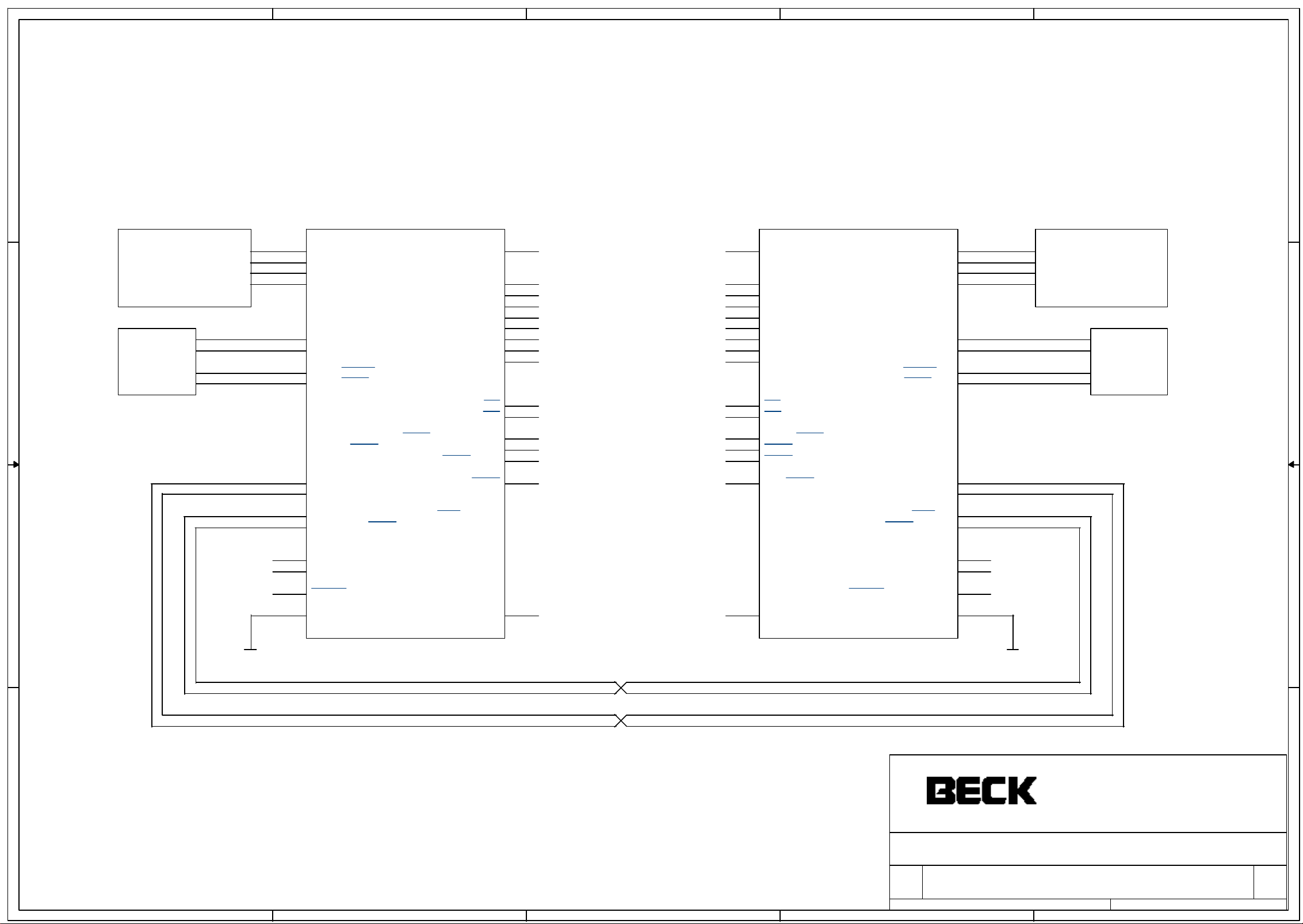
5
4
3
2
1
Ethernet to Ethernet Router
D D
IC1
IPC@CHIP SC12
18
TPTX+
19
TPTX-
20
TPRX+
21
TPRX-
IC1
10BaseT
2
TXD0/P8
1
C C
IC1
EXT0
RXD0/P7
3
CTS0/ENRX0/P9
4
RTS0/RTR0/P10
MCS0/PCS1/P4/TMRIN0/A0
PCS5/P3/TMROUT1/TMRIN1/A1
5
TXD1/P11
6
RXD1/INT3/P12
25
CTS1/MEN/PCS2/P6/INT2/INTA/PW
26
RTS1/MOSI/PCS3/P5/INT4
PCS6/P2/A2
ALE/PCS0
VCC
AD0
AD1
AD2
AD3
AD4
AD5
AD6
AD7
RD
WR
32
8
9
10
11
12
13
14
15
22
23
27
28
29
24
IC2
IPC@CHIP SC12
32
VCC
8
AD0
9
AD1
10
AD2
11
AD3
12
AD4
13
AD5
14
AD6
15
AD7
22
RD
23
WR
27
MCS0/PCS1/P4/TMRIN0/A0
28
PCS5/P3/TMROUT1/TMRIN1/A1
29
PCS6/P2/A2
24
ALE/PCS0
CTS1/MEN/PCS2/P6/INT2/INTA/PW
RTS1/MOSI/PCS3/P5/INT4
TPTX+
TPTX-
TPRX+
TPRX-
TXD0/P8
RXD0/P7
CTS0/ENRX0/P9
RTS0/RTR0/P10
TXD1/P11
RXD1/INT3/P12
18
19
20
21
2
1
3
4
5
6
25
26
IC2
10BaseT
IC2
EXT0
31
I2CCLK/MSCK/DRQ1/INT6/P0
30
B B
GND
I2CDAT/MISO/DRQ0/INT5/P1
17
RESET_PFAIL_LILED
16 7
GND TMROUT0/INT0/P13
IC1_RTS1
IC1_CTS1
IC1_RXD1
IC2_RTS1
IC2_CTS1
IC2_RXD1
IC2_TXD1IC1_TXD1
I2CCLK/MSCK/DRQ1/INT6/P0
I2CDAT/MISO/DRQ0/INT5/P1
RESET_PFAIL_LILED
GNDTMROUT0/INT0/P13
31
30
17
167
GND
high speed communication
A A
with serial port DMA
Title
IPC@CHIP SC12 circuit example
Size Document Num ber Re v
A4
5
4
3
Date: Sheet of
2
(c) 1996 - 99 CHIP D1
IPC GmbH
Germany - 35578 Wetzlar
Garbenheimer Str asse 38
0.5
1 1Tuesday, November 23, 1999
1
Page 36
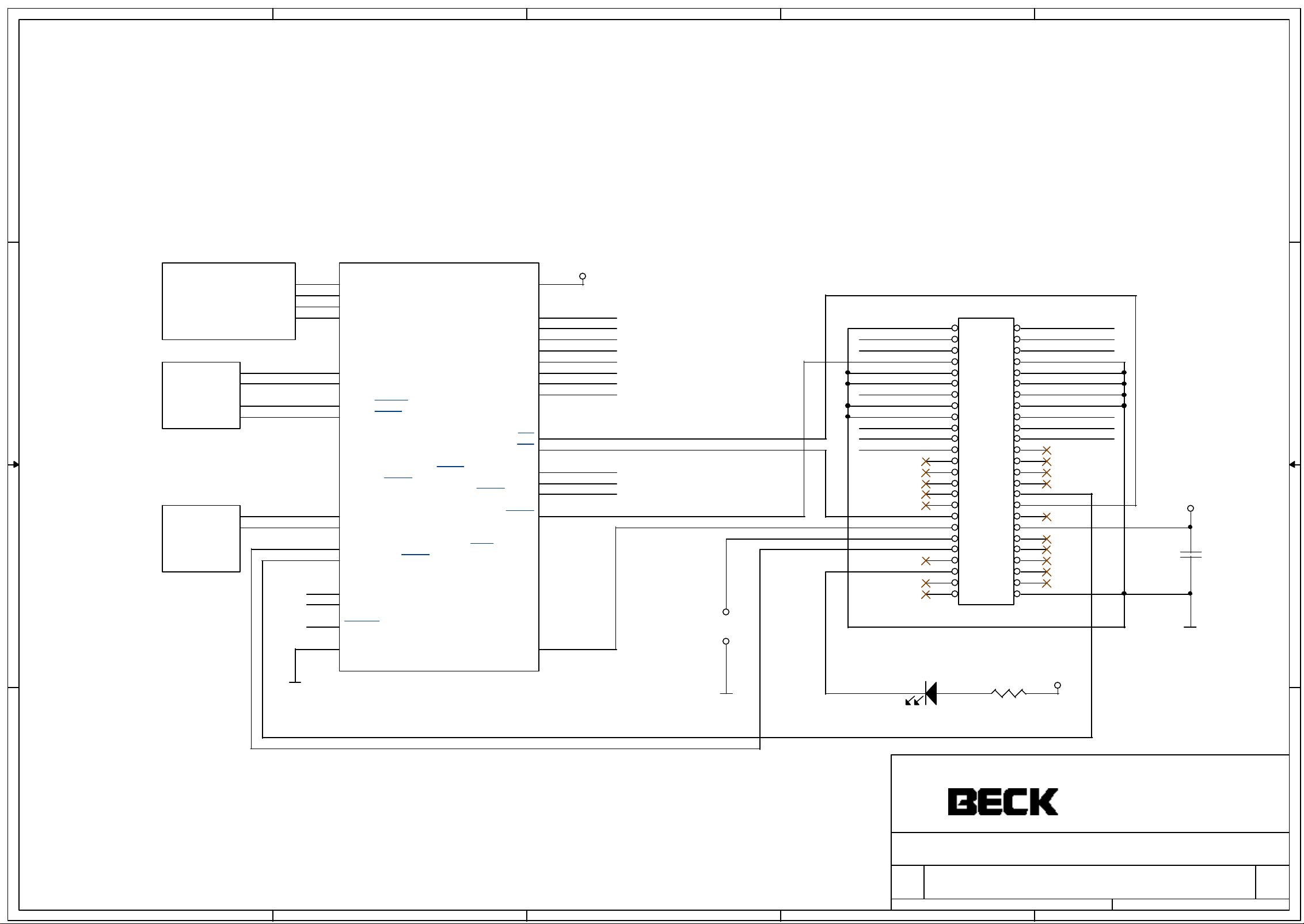
5
4
3
2
1
8bit compact
D D
flash disk
IC1
IPC@CHIP SC12
18
TPTX+
19
TPTX-
20
TPRX+
21
TPRX-
C C
2
TXD0/P8
1
RXD0/P7
3
CTS0/ENRX0/P9
4
RTS0/RTR0/P10
VCC
MCS0/PCS1/P4/TMRIN0/A0
PCS5/P3/TMROUT1/TMRIN1/A1
PCS6/P2/A2
5
TXD1/P11
6
RXD1/INT3/P12
EXT1 10BaseTEXT0
B B
RESET#
PCS3#
25
CTS1/MEN/PCS2/P6/INT2/INTA/PW
26
RTS1/MOSI/PCS3/P5/INT4
31
I2CCLK/MSCK/DRQ1/INT6/P0
30
I2CDAT/MISO/DRQ0/INT5/P1
17
RESET_PFAIL_LILED
16 7
GND TMROUT0/INT0/P13
ALE/PCS0
AD0
AD1
AD2
AD3
AD4
AD5
AD6
AD7
RD
WR
32
8
9
10
11
12
13
14
15
22
23
27
28
29
24
D0
D1
D2
D3
D4
D5
D6
D7
RD#
WR#
A0
A1
A2
CE1#
INT0
JP1
JUMP2
ON = Master
GND
D4 D5
D6 D7
CE1#
OE#
A8 A7
+5V
A5 A4
A3
A1 A0
D0 D1
D2
BD11
BD13
BD15
WR#
INT0
M_SLAVE
RESET#
DASP
BD8
BD10
1 2
3 4
5 6
7 8
9 10
11 12
13 14
15 16
17 18
19 20
21 22
23 24
25 26
27 28
29 30
31 32
33 34
35 36
37 38
39 40
41 42
43 44
45 46
47 48
49 50
A10
A9
A6
IOIS16#
BD12
BD14
IORDY
PDIAG#
BD9
CFD50A
ST1
D3
A2
CE2#
RD#
+5V
GND
VCC
C1
0.1uF
GND
VCC
L1
R1
VCC
GNDGND
LEDGR390
390E
IPC GmbH
A A
Germany - 35578 Wetzlar
Garbenheimer Stra sse 38
Title
IPC@CHIP SC12 circuit example
Size Document Numb er Rev
A4
5
4
3
Date: Sheet of
2
(c) 1996 - 99 CHIP D1
1 1Tuesday, November 23, 1999
1
0.5
Page 37
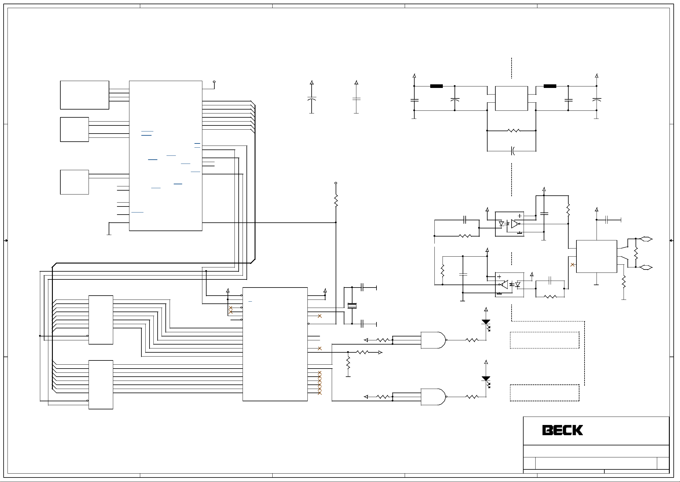
5
4
3
2
1
82527 CAN bus master
D D
10BaseTEXT0EXT1
C C
GND
IC2
B B
A A
AD0
AD1
AD2
AD3
AD4
AD5
AD6
AD7
PCS1#
ALE
AD0
AD7
PCS1#
RD#
3
4
7
8
13
14
17
18
1
11
2
3
4
5
6
7
8
9
19
1
74HCT373
D0
D1
D2
D3
D4
D5
D6
D7
OC
G
IC3
74HCT245
A1
A2
A3
A4
A5
A6
A7
A8
G
DIR
Q0
Q1
Q2
Q3
Q4
Q5
Q6
Q7
B1
B2
B3
B4
B5
B6
B7
B8
IC1
IPC@CHIP SC12
18
TPTX+
19
TPTX-
20
TPRX+
21
TPRX-
2
TXD0/P8
1
RXD0/P7
3
CTS0/ENRX0/P9
4
RTS0/RTR0/P10
MCS0/PCS1/P4/TMRIN0/A0
PCS5/P3/TMROUT1/TMRIN1/A1
5
TXD1/P11
6
RXD1/INT3/P12
25
CTS1/MEN/PCS2/P6/INT2/INTA/PW
26
RTS1/MOSI/PCS3/P5/INT4
31
I2CCLK/MSCK/DRQ1/INT6/P0
30
I2CDAT/MISO/DRQ0/INT5/P1
17
RESET_PFAIL_LILED
16 7
GND TMROUT0/INT0/P13
2
5
6
9
12
15
16
19
18
17
16
15
14
13
12
11
PCS6/P2/A2
ALE/PCS0
A0
A1
A2
A3
A4
A5
A6
A7
D0
D1
D2
D3
D4
D5
D6
D7
VCC
AD0
AD1
AD2
AD3
AD4
AD5
AD6
AD7
RD
WR
32
8
9
10
11
12
13
14
15
22
23
27
28
29
24
VCC
PCS1#
WR#
AD0
AD1
AD2
AD3
AD4
AD5
AD6
AD7
RD#
WR#
PCS1#
ALE
INT0
VCC
VCC +5V
VCCVCC
+ C58
4u7/10V
VCC
R13
10k
IC4
8
CS
6
E
7
R/W
9
DSACK0
28
READY
5
AS
29
RESET
4
A0
3
A1
2
A2
43
A3
42
A4
41
A5
40
A6
39
A7
38
D0
37
D1
36
D2
35
D3
34
D4
33
D5
32
D6
31
D7
82527
MODE0
MODE1
XTAL1
XTAL2
CLKOUT
TX0
RX0
TX1
RX1
P2.0
P2.1
P2.2
P2.3
P2.4
P2.5
P2.6
P2.7
INT
VCC
44
30
18
19
27
24
26
22
25
21
17
16
15
14
13
12
11
10
R21
47k
GND
GNDGND
12
C59
22p
16.00MHz
C64
22p
VCC
47k
VCC
C65
100N
Q1
QUARZ
R22
10k
GND 0V
GND
GND
R24
10k
VCC
R23
10
11
3
4
5
9
C67
100n
IC19B
74HCT10
IC19C
74HCT10
L2
100uH
6
8
R20
1k
+ C68
4u7/10V
R16
390
GND
C57
56p
R19
390
R18
390
C62
100n
VCC
VCC
VCC
VCC
IC5
2
VCC
1
GND
NME0505_SIL
OP2
2
3
HCPL2601
OP1
8
7
6
5
HCPL2601
D7
LED
D8
LED
R14
1M
C60
2n2/400V
L1
suppression filter
4
+V
3
0V
+5V
8
7
6
5
+5V
2
3
red error LED
yellow indication LED
Title
C61
100n
0V
C56
56p
R17
390
+ C55
C66
100n
R15
1k
IC6
82C250
1
TXD
4
RXD
5 8
REF RS
4u7/10V
+5V
C63
100n
CANH
CANL
GND VCC
2 3
0V
R26
10
IPC GmbH
Germany - 35578 Wetzlar
Garbenheimer Strasse 38
0V
CANH
7
6
0V
R25
150
CANL
IPC@CHIP SC12 circuit e xample
Size Document Number Rev
A3
5
4
3
2
Date: Sheet of
(c) 1996 - 99 CHIPD1
1
1 1Tuesday, November 23, 1999
0.5
 Loading...