

Page 1
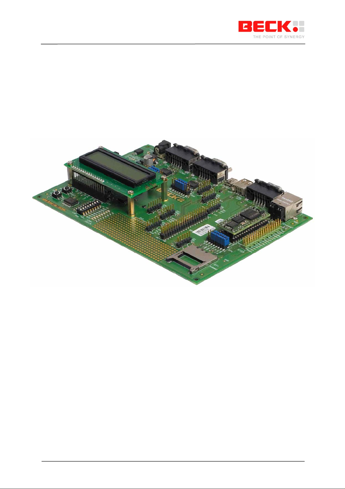
IPC@CHIP DB54
Hardware Manual V1.1 [04.10.2007]
Hardware Manual
IPC@CHIP Development Board
DB54
High Performance IPC@CHIP SC23
Embedded Web Controller
Order No. IPC@CHIP
Development Board DB54:
Development Kit DK55:
©2000-2008 Beck IPC GmbH Page 1 of 24
553946
553947
Page 2

IPC@CHIP DB54
Hardware Manual V1.1 [04.10.2007]
Copyright & Trademark
IPC@CHIP® is a registered trademark of Beck IPC. Ethernet is a
registered trademark of Xerox Corporation. All other product names,
company names, logos or other symbols referred to herein are trademarks
of their respective owners.
Ethernet is a registered trademark of Xerox Corporation.
SPI is a trademark of Motorola, Inc.
No part of this guide may be reproduced or transmitted in any form for any
purpose whatsoever other than the purchaser's personal use, without the
express written permission of Beck IPC.
Beck IPC GmbH
Grüninger Weg 24
35415 Pohlheim-Garbenteich / Germany
Phone: +49 6404 695-0
Fax: +49 6404 695-500
Technical Support
Phone: +49 6404 695-200
Fax: +49 6404 695-515
Online:
www.beck-ipc.com
E-mail: [email protected]
©2000-2008 Beck IPC GmbH Page 2 of 24
Page 3

IPC@CHIP DB54
Hardware Manual V1.1 [04.10.2007]
Table of Contents
1. OVERVIEW...................................................................................................................................................... 4
1.1 INTRODUCTION .............................................................................................................................................. 4
1.2 ACCESSORIES.................................................................................................................................................4
1.3 GETTING STARTED.........................................................................................................................................4
2. BLOCK DIAGRAM......................................................................................................................................... 5
3. PLACEMENT DIAGRAM .............................................................................................................................. 6
4. ELECTRICAL FUNCTIONS / INTERFACES.............................................................................................7
4.1 POWER SUPPLY...............................................................................................................................................7
4.2 ST12 & S1 - POWER SUPPLY CONNECTOR...................................................................................................... 7
4.3 SW1 - 24V SWITCH........................................................................................................................................ 7
4.4 SW18 - POWER-FAIL BUTTON ........................................................................................................................ 8
4.5 SW19 - RESET BUTTON.................................................................................................................................. 8
4.6 LED’S AND DIP SWITCH................................................................................................................................8
4.7 LC-DISPLAY .................................................................................................................................................. 9
4.8 S39 - PIN HEADER WITH POWER SUPPLIES .................................................................................................... 10
4.9 IC11 - IPC@CHIP SC23 SOCKET................................................................................................................ 10
4.10 ST23 - IPC@CHIP SC23 PIN HEADER ....................................................................................................... 11
4.11 S9, S31, S32 - WLAN SUPPORTING PIN HEADERS ...................................................................................... 11
4.12 S30 - I2C INTERFACE ................................................................................................................................. 13
4.13 ST15 - RS232 INTERFACE COM1 .............................................................................................................. 13
4.14 S41 - JUMPER ARRAY COM1 ..................................................................................................................... 14
4.15 ST14 - RS232 INTERFACE COM2 .............................................................................................................. 15
4.16 S40 - JUMPER ARRAY COM2 ..................................................................................................................... 15
4.17 S42 - DCD, DTR, DSR CONNECTOR ......................................................................................................... 16
4.18 S32 - SERIAL INTERFACE COM3 / SPI........................................................................................................ 16
4.19 ST1 - SD/MMC INTERFACE ....................................................................................................................... 17
4.20 ST4 - PIO JUMPER ARRAY.......................................................................................................................... 17
4.21 ST3 - ETHERNET INTERFACE ...................................................................................................................... 18
4.22 S6 - CAN0 INTERFACE............................................................................................................................... 18
4.23 S38 - CAN1 (COM2) INTERFACE............................................................................................................... 19
4.24 ST16 & ST13 - USB INTERFACE................................................................................................................ 20
5. TECHNICAL DATA...................................................................................................................................... 22
5.1 CLIMATIC DATA ........................................................................................................................................... 22
5.2 MECHANICAL DATA ..................................................................................................................................... 22
5.3 ELECTROMAGNETIC DATA............................................................................................................................ 22
5.4 ELECTRICAL DATA ....................................................................................................................................... 22
6. GENERAL CONDITIONS OF USE............................................................................................................. 23
6.1 SCOPE OF APPLICATION................................................................................................................................23
7. EXCLUSION OF WARRANTY AND LIABILITY.................................................................................... 23
8. HISTORY........................................................................................................................................................ 24
©2000-2008 Beck IPC GmbH Page 3 of 24
Page 4

IPC@CHIP DB54
Hardware Manual V1.1 [04.10.2007]
1. Overview
1.1 Introduction
The IPC@CHIP® SC23 Embedded Web Controller has been d esigned to meet the most common requirements
of embedded products developed for the communication, office automation, mass storage, and general
embedded markets. Specific applications would inclu de industrial controls, data collection, protocol conversion,
process monitoring and Internet connectivity.
The IPC@CHIP® SC1X3 family is a combination of hardware and software including the preinstalled real-time
Operating System, TCP/IP stack, web server, FTP server and Telnet server. It offers increased reliability,
functionality and performance, and considerabl y reduced time to market, and also enables designers to reduce
the size, power consumption and cost of the embedded system.
The IPC@CHIP® SC23 microcontrollers also integrate the functions of the CPU, two independent timers,
watchdog timer, interrupt controller, DMA controller, three asynchronous serial ports, and programmable I/O pins
on one chip. It also supports the I²C bus and SPI (Serial Peripheral Interface). The USB interface supports userspecific connections to standard USB hosts like PCs (USB device mode) or memory expansion with USB sticks
(USB host mode).
The DB54 development board is designed to provide an easy introduction to the SC23 technology, both for
software development in C/C++ and in IEC61131. It also provides a hardware basis for quickly developing a
functional prototype for your product. The DB54 can also be expanded ea sily using a plug-in board.
including a breadboard area for customer-specific extensions
1.2 Accessories
The following accessories are not supplied with the Development Board DB54, but can be order ed separately:
Order number: Accessories:
195837 ZK14 serial programming cable
538934 PSE10 power supply for DB54
541522 Paradigm C/C++ Beck IPC Edition
1.3 Getting Started
The initial commissioning of the DB54 and the software and tools required for this are described in the document
IPC@CHIP® SC123 “Getting Started”. This is available from the Internet at:
http://www.beck-ipc.com/ipc/gettingstarted
This web page also provides links to the required tools as well as other useful docume ntation (SC1xx Hardware
Manual; RTOS API documentation).
©2000-2008 Beck IPC GmbH Page 4 of 24
Page 5
IPC@CHIP DB54
Hardware Manual V1.1 [04.10.2007]
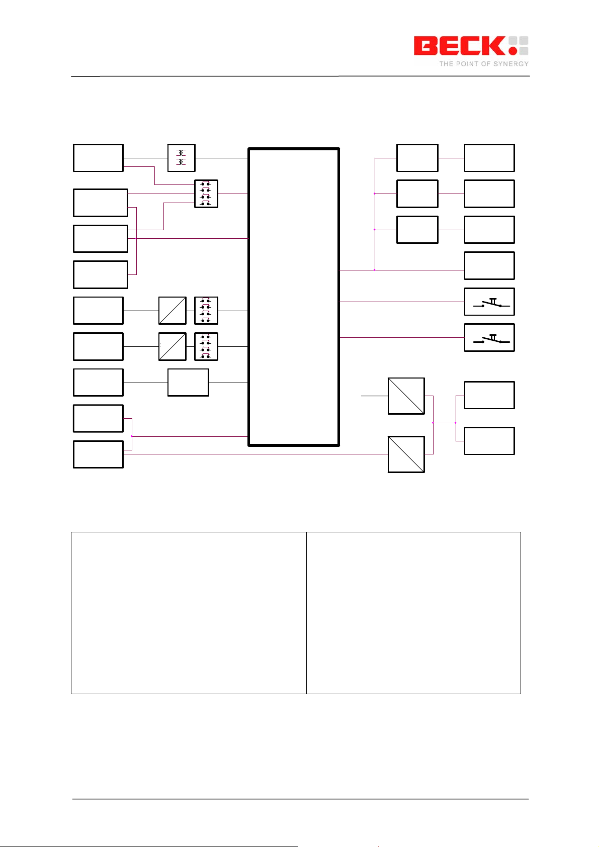
2. Block diagram
ETH0
100/10 Base T
FK61-WL01
support
MMC/SD-Card
Interface
COM3/SPI/GPIO
COM2
Serial RS232
Interface
DSUB male
COM1
Serial RS232
Interface
DSUB male
DSUB female
USB Device
LED
pin header
CAN0
USB-B
USB Host
USB-A
GPIO
GPIO
GPIO
RS232
CAN-Bus
pinheader/jumper
5V
SPI
RS232
TTL
RS232
TTL
CAN
Transceiver
USB
Ethernet
pinheader/
jumper
pinheader/
jumper
GPIO
TTLRS232
TTL
TTL
IPC@CHIP
SC23
I2C-Bus
reset
PFI
+3V3 / 1A
+5V / 500mA
I2C Port
Expander
I2C Port
Expander
I2C Port
Expander
DC-Converter
9..30V DC
3V3/1A
DC-Converter
9..30V DC
5V/500mA
8 bit IN
switch
8-bit in-/out port
8 bit OUT
LED's
LC-Display
I2C/GPIO
pin header
Reset-Button
Power-Fail-Button
DC-Connector
Alternate DC
Connector
DB54 features are:
• Embedded Web Controller SC23
• 9..30V power supply input, protected against
reverse polarity
• Power LED
• 3.3V and 5V power supply
• Reset button
• Power-fail button (for power fail emulation)
• 3 serial interfaces (of which two with RS232 level)
• 2 CAN interfaces (one with CAN transceiver)
• USB interface (host / device)
• SPI interface
• I2C interface
• 10/100 Base-T Ethernet interface with
status LEDs
• SD/MMC socket
• 8-way LEDs port
• 8-way DIP switch
• Expansion pin header
• GPIO pins
• LC-Display
©2000-2008 Beck IPC GmbH Page 5 of 24
Page 6
IPC@CHIP DB54
Hardware Manual V1.1 [04.10.2007]
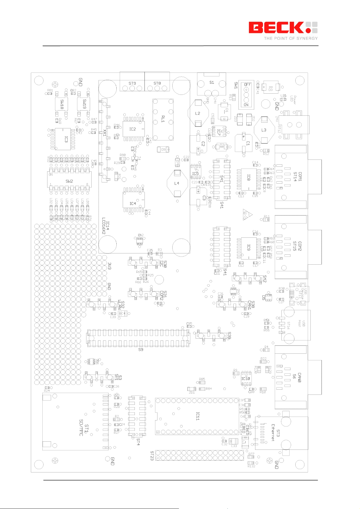
3. Component layout diagram
©2000-2008 Beck IPC GmbH Page 6 of 24
Page 7
IPC@CHIP DB54
Hardware Manual V1.1 [04.10.2007]
4. Electrical Functions / Interfaces
4.1 Power supply
The 24V power supply input of the DB54 is protected against reverse polarity and transient over-voltages. An
operating voltage indication (LD1) is located near the power supply socket. Dimming of th e power indication LED
signals reset of the SC23.
A switching controller from the 9...30V DC power supply of the DB54 is used to provide the internal 3.3V po wer
supply. This voltage is also provided at different pin header for external expansions, the 3.3V s witching controll er
can supply 600mA for external expansions. In the basic configuration, the maximum internal load of the 3.3V
power supply is 400mA. An additional switching controller provides 5V/500mA from the 24V operating voltage of
the DB54 for the USB host function.
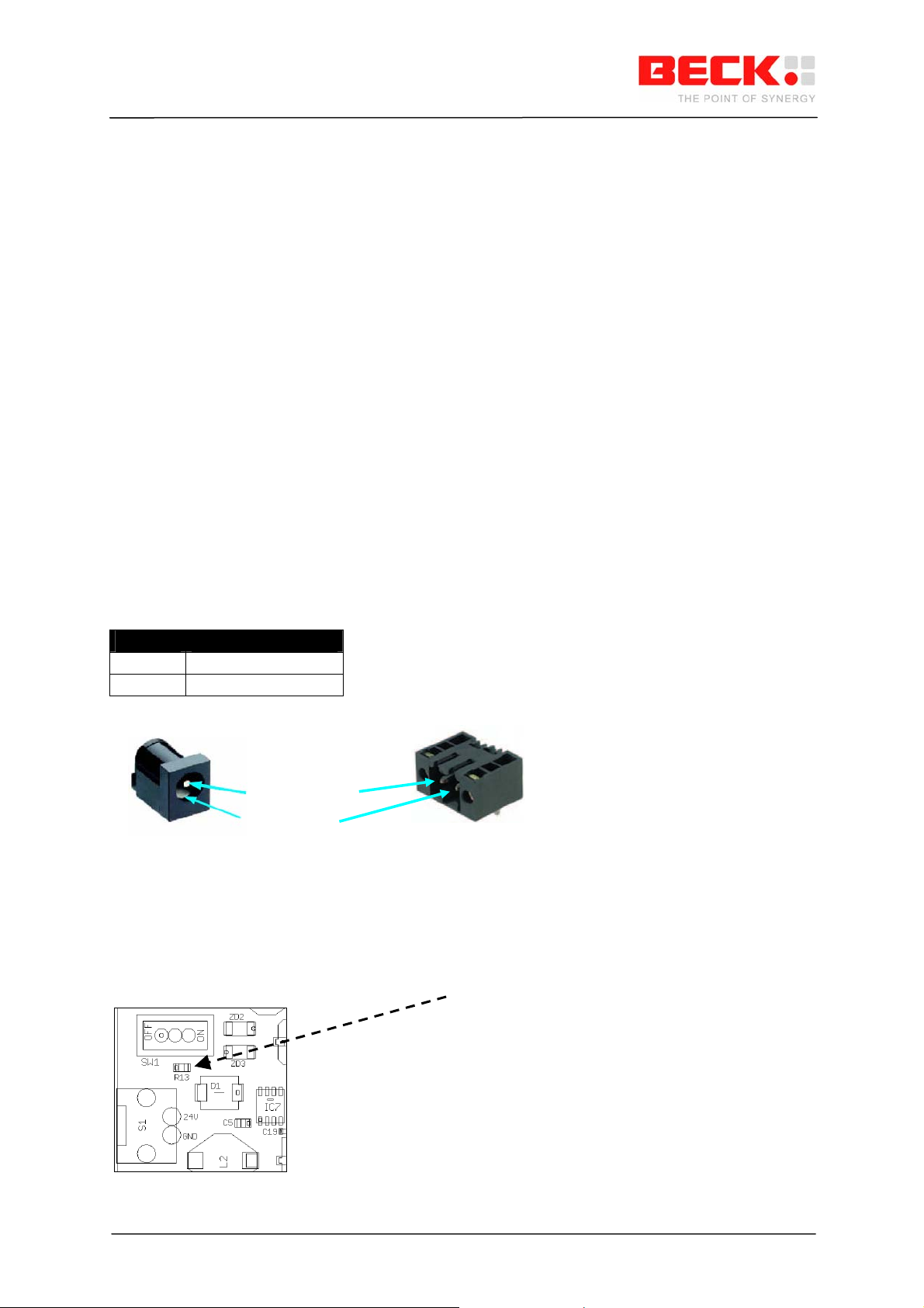
4.2 ST12 & S1 - Power supply connector
Power supply connectors for the DB54
Pin assignment:
Pin No. Designation
1 (pin) 24V DC (9..30V DC)
2 (shield) GND
9..30V DC (pin)
GND (shiel
d)
4.3 SW1 - 24V switch
Switch for the operating voltage of the DB54
Not assembled / optional assignment: e.g. APEM 25136NAH silver ON-ON
If the switch is to be assembled later, the 0 Ohm R13 resistor near the SW1must be removed.
Top view
©2000-2008 Beck IPC GmbH Page 7 of 24
Page 8
IPC@CHIP DB54
Hardware Manual V1.1 [04.10.2007]
4.4 SW18 - Power-fail button
Pressing the PFI button (SW18) emulates a power-fail event if the Power-fail function is enabled in the SC23, and
calls a power-fail software routine. This routine can write data to the Flash memory area of the SC23. The Powerfail function must be software-enabled (CHIP.INI or software interrupt). Using the PIO9 function of the PFI/PIO9
signal, the PFI button can also be used as a push-button for input.
4.5 SW19 - Reset button
Power-on reset and the reset button (SW19) generate a low active reset pulse for the SC23 processor.
4.6 LED’s and DIP switch
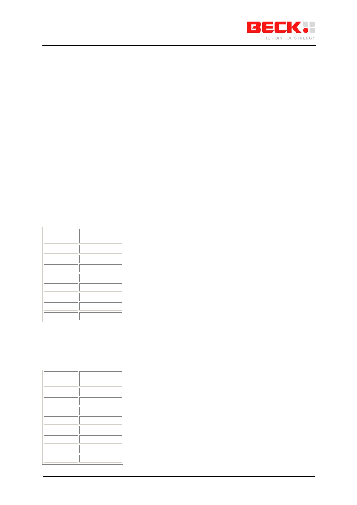
For digital input and output simulation
The DIP-switch is connected to an I2C I/O port expander (PCF8574A). It is coded to the I2C base
address 72hex. A switch in the ON position will read out logic 0, and a switch in the OFF position will
read out logic 1. Using the I2C port expander it ispossible to have a practical expansion of input and
output signals for the SC23.
switch
BIT7 D7
BIT6 D6
BIT5 D5
BIT4 D4
BIT3 D3
BIT2 D2
BIT1 D1
BIT0 D0
PCF8574A
I/O expander
The LED’s are connected to an I2C I/O port expander (PCF8574A). It is coded t o the I2C base
address 70hex. To light up an LED you have to write logic 0 to the correspondi ng port bit, and to
switch the LED off you need a logic 1 at the port bit.
LED
BIT7 D7
BIT6 D6
BIT5 D5
BIT4 D4
BIT3 D3
BIT2 D2
BIT1 D1
BIT0 D0
©2000-2008 Beck IPC GmbH Page 8 of 24
PCF8574A
I/O expander
Page 9
IPC@CHIP DB54
Hardware Manual V1.1 [04.10.2007]
A sample program for handling the LED’s and DIP-switch can be obtained from the BECK IPC
website.
4.7 LCD Display
For more complex visualization, a two-row, 16 character dot matrix, LCD (without backlight) with
KS0066 controller/driver is provided on the DB54.
This is an easy way to interface 5V technology and expand the I/O capabilities of the SC23.
The LCD is interfaced to an I2C port expander to the SC23 and uses the 4-bit mode. The I2C address
of the LCD interface is 74hex.
Sample programs for handling the LCD can be obtained from the BECK IPC website.
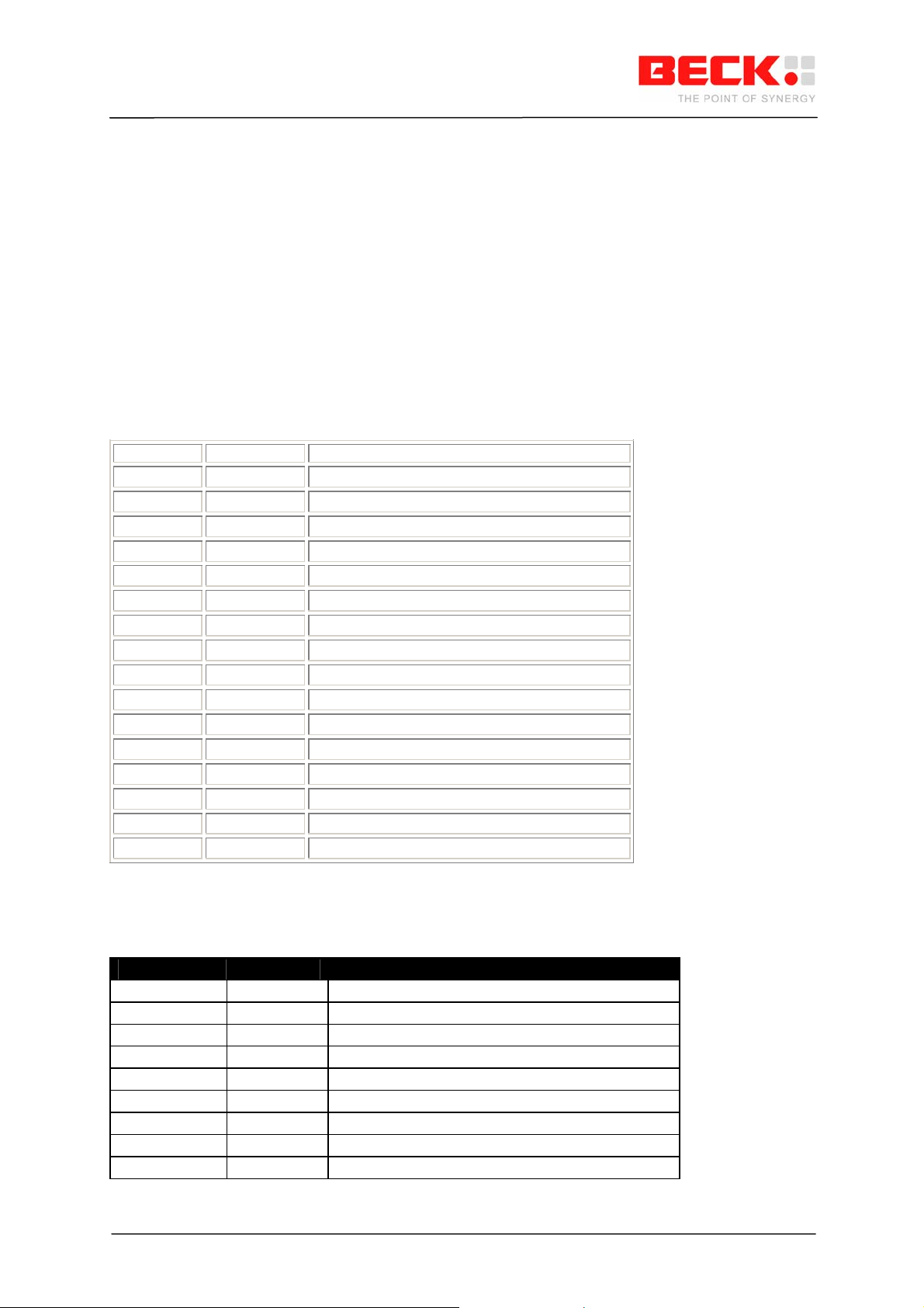
Pin assignment (Display pins)
Board Pin Display Pin Name
1 14 D7
2 16 D6
3 1 D5
4 2 D4
5 3 D3
6 4 D2
7 5 D1
8 6 D0
9 7 E
10 8 R/W
11 9 RS
12 10 VEE
13 11 VDD
14 12 GND
15 13 LCD_LED_K
16 15 LCD_LED_A
Signal descriptions of the asynchronous serial interface:
Signal name Direction Description
Vss GND
Vdd +5V power supply
Vee Display voltage (contrast)
RS Input Register select
R/W Input
E Input
DB0..DB7 Input/Output
LED_A Backlight LED + (Not assembled)
LED_K Backlight LED - (Not assembled)
©2000-2008 Beck IPC GmbH Page 9 of 24
Page 10
IPC@CHIP DB54
Hardware Manual V1.1 [04.10.2007]
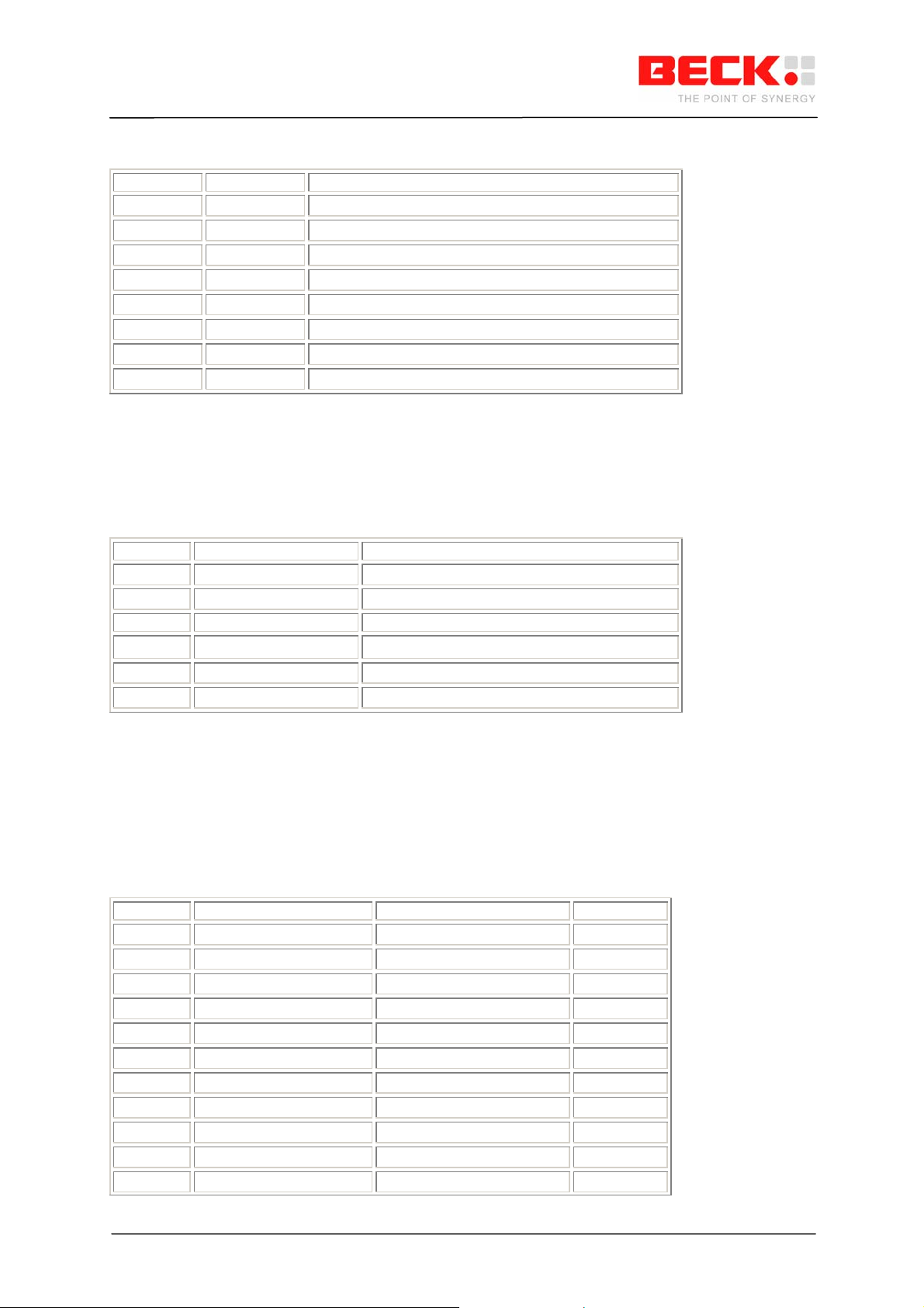
I2C I/O port expander PCF8574A to LCD assignment:
I2C Port Display Name
D0 LCD_D4 D4
D1 LCD_D5 D5
D2 LCD_D6 D6
D3 LCD_D7 D7
D4 LCD_R/W 1 = read from LCD / 0 = write to LCD
D5 LCD_RS Register select
D6 LCD_E 1 = data enable. LCD reads data with falling edge
D7 LCD_LED (No function) Backlight
4.8 S39 - Pin header with power supplies
This pin header can be used for accommodating all the power supp lies of the DB54.
Pin assignment (1x6 pin header, pitch 2.54mm)
Pin No. Name Description
1 +24V (9..30V DC) DB54 board power supply
2 GND
3 +5V 5V power supply for USB host, CAN
4 VCC_USB_DEVICE Voltage input of USB Device Interface
5 +3.3V 3.3V logic voltage
6 GND
4.9 IC11 - IPC@CHIP SC23 Socket
Socket for the IPC@CHIP SC23 module
The SC23 is described in the SC2x Hardware Manual
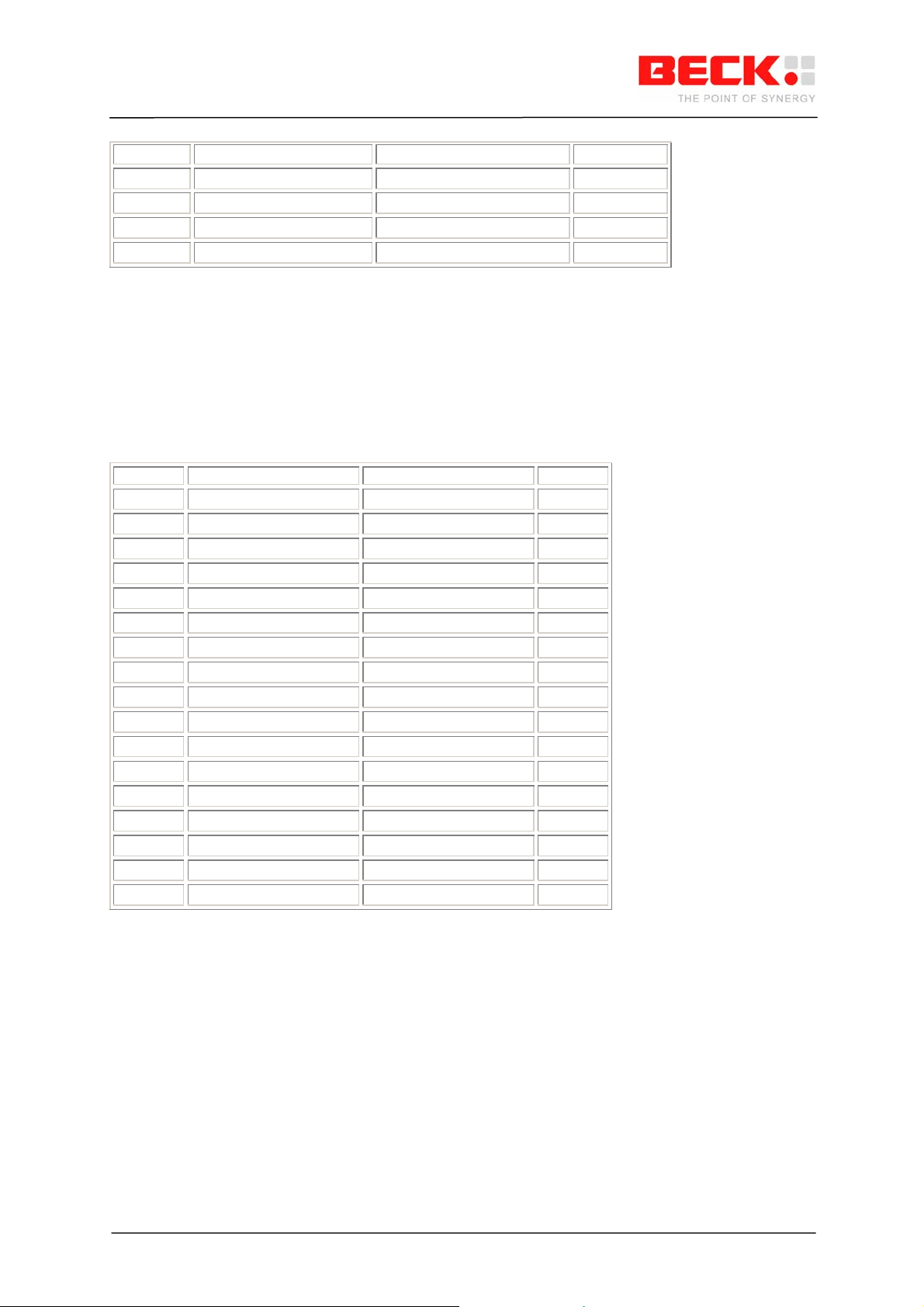
Pin assignment (32 pin IC socket)
Pin No. Name Description Pin No.
1 RXD1 PFI/PIO9 32
2 TXD1 TMRIN1/INT5#/PIO0 31
3 CTS1#/PIO12 TMROUT1/INT3/PIO1 30
4 RTS1 TMROUT0/PIO10 29
5 TXD2/PIO22 TMRIN0/PIO11 28
6 RXD2/PIO23 INT1/PIO2 27
7 CTS2#/CAN1RX/PIO12 RESETOUT# 26
8 RTS2#/CAN1TX/PIO20 I2CCLK/PIO31 25
9 RXD3/SDI/PIO28 I2CSDA/PIO13 24
10 TXD3/SDO/PIO27 CAN0RX 23
11 RTS3#/SCK/PIO19 CAN0TX 22
©2000-2008 Beck IPC GmbH Page 10 of 24
Page 11
IPC@CHIP DB54
Hardware Manual V1.1 [04.10.2007]
12 CTS3/SEL/PIO18 TPRX- 21
13 USBP TPRX+ 20
14 USBN TPTX- 19
15 3V3 TPTX+ 18
16 GND RESETIN#/TRAFFIC 17
4.10 ST23 - IPC@CHIP SC23 pin header
Pin header for SC23 expansion or measurement.
To avoid low Ethernet quality, the Ethernet signals are not connected to this pin header.
Pin assignment (2x17 pin header, pitch 2.54mm)
Pin No. Name Description Pin No.
1 RXD1 PFI/PIO9 34
2 TXD1 TMRIN1/INT5#/PIO0 33
3 CTS1#/PIO12 TMROUT1/INT3/PIO1 32
4 RTS1 TMROUT0/PIO10 31
5 TXD2/PIO22 TMRIN0/PIO11 30
6 RXD2/PIO23 INT1/PIO2 29
7 CTS2#/CAN1RX/PIO12 RESETOUT# 28
8 RTS2#/CAN1TX/PIO20 I2CCLK/PIO31 27
9 RXD3/SDI/PIO28 I2CSDA/PIO13 26
10 TXD3/SDO/PIO27 CAN0RX 25
11 RTS3#/SCK/PIO19 CAN0TX 24
12 CTS3/SEL/PIO18 NC 23
13 USBP NC 22
14 USBN NC 21
15 3V3 NC 20
16 GND RESETIN#/TRAFFIC 19
17 NC NC 18
4.11 S9, S31, S32 - WLAN supporting pin headers
The S9 pin header in conjunction with S31 and S32 supports the usability of the FK61-WL01 WLAN
module with the DB54 Board. The FK61-WL01 WLAN module uses the SPI interface at S32 and three
PIO pins at S9. To allow WLAN and SD/MMC to coexist at the SPI bus, the WLAN interface uses a
different SPI slave select signal (PIO12 / CTS1), so the CTS1 jumper must be removed from S41 for
the use of the FK61-WL01 module.
©2000-2008 Beck IPC GmbH Page 11 of 24
Page 12
IPC@CHIP DB54
Hardware Manual V1.1 [04.10.2007]
Pin assignment of S9 (2x20 pin header, pitch 2.54mm):
Pin No. Name Description Pin No.
1 VCC (+3.3V) NC 2
3 GND NC 4
5 NC NC 6
7 Reserved NC 8
9 Reserved NC 10
11 Reserved NC 12
13 NC NC 14
15 NC NC 16
17 WLAN_INT# NC 18
19 NC NC 20
21 NC NC 22
23 NC NC 24
25 NC NC 26
27 NC NC 28
29 NC NC 30
31 NC NC 32
33 NC NC 34
35 WLAN_SEL# NC 36
37 WLAN_RES# NC 38
39 NC NC 40
Signal descriptions of the expansion interface:
Signal name Direction Description
WLAN_INT# Input INT5# (PIO0 / TMRIN1)
WLAN_SEL# Output PIO12 (CTS1)
WLAN_RES# Output PIO2 (INT1)
WLAN SPI Connector
Pin assignment (1x6 pin header, pitch 2.54mm)
Pin No. Name
1 VCC
2 GND
3 SDO (TXD3 / PIO27)
4 SDI (RXD3 / PIO28)
5 PIO12 (CTS1)
6 SCK (RTS3 / PIO19)
©2000-2008 Beck IPC GmbH Page 12 of 24
Page 13
IPC@CHIP DB54
Hardware Manual V1.1 [04.10.2007]
Signal descriptions:
Signal name Direction Description
TXD3
PIO27
SDO
Output
Bi-directional
Output
Serial data Transmit line. TTL level
PIO27
SDO (serial data out)
SC23 as SPI master: MOSI
SC23 as SPI slave: MISO
RXD3
PIO28
SDI
PIO12
CTS1
RTS3
PIO19
SCK
VCC 3.3 power supply
GND GND, Signal reference
Input
Bi-directional
Input
Bi-directional
Input
Output
Bi-directional
Output
Serial data Receive line. TTL level
PIO28
SDI (serial data in)
SC23 as SPI master: MISO
SC23 as SPI slave: MOSI
SPI Slave Select
Handshake line. Clear To Send. TTL level
Handshake line. Request To Send. TTL level
PIO19
SPI clock
(e.g. for externally connected level converter)
4.12 S30 - I2C Interface
Alternatively PIO signals can also be configured on the signals of the I2C interface.
1 K Ohm pull-up resistors are connected on SDA and SCL
Pin assignment (pin header pitch 2.54mm):
Pin No. Name
1 VCC
2 GND
3 I2CSDA (P13)
4 I2CCLK (P31)
5 NC
6 NC
Signal descriptions of the I2C interface:
Signal name Direction Description
I2CDTA
P13
I2CCLK
P31
VCC 3.3V power supply for externally connected
GND Signal reference
Bi-directional
Bi-directional
Output
Bi-directional
Serial data
PIO13
Clock
PIO31
expansion
4.13 ST15 - RS232 interface COM1
Asynchronous serial interface with RS232 / V24 level and transfer rates up to max. 115200 baud.
©2000-2008 Beck IPC GmbH Page 13 of 24
Page 14
IPC@CHIP DB54
Hardware Manual V1.1 [04.10.2007]
The default function of this interface is the terminal interface (19200 baud, lines used: TXD, RXD)
This interface can also be used for RTOS update (Interface settings for RTOS update 115 KBaud,
lines used: TXD, RXD)
Pin assignment (D-SUB 9-pole male connector):
Pin No. Name
1 NC
2 RXD1
3 TXD1
4 NC
5 GND
6 NC
7 RTS1
8 CTS1 (PIO12)
9 NC
Signal descriptions of the asynchronous serial interface:
Signal name Direction Description
TXD1 Output Serial data Transmit line. RS232/V24 level
RXD1 Input Serial data Receive li ne. RS232/V24 level
CTS1 Input Handshake line. Clear To Send. RS232/V24 level
RTS1 Output Handshake line. Request To Send. RS232/V24 level
GND GND, Signal reference
4.14 S41 - Jumper array COM1
A jumper placed at this pin header allows the serial interfaces of the SC23 to be used with an RS232
level. Removing the jumpers allows the serial signals to be used directly as TTL levels e.g. for RS485
driver.
Pin assignment (2x8 pin header, pitch 2.54mm)
Pin No. Name Description Pin No.
1 NC VCC (3.3V) 2
3 NC GND 4
5 TXD1 to RS232 level converter TXD1-TTL 6
7 RXD1 from RS232 level converter RXD1-TTL 8
9 CTS1 from RS232 level converter CTS1-TTL (PIO12) 10
11 RTS1 to RS232 level convert er RTS1-TTL 12
13 NC NC 14
15 NC NC 16
©2000-2008 Beck IPC GmbH Page 14 of 24
Page 15
IPC@CHIP DB54
Hardware Manual V1.1 [04.10.2007]
4.15 ST14 - RS232 Interface COM2
Asynchronous serial interface with RS232 / V24 level and transfer rates up to max. 115200 baud.
Two jumpers at S42 can be used to connect pins 1, 4 and 6 (DCD, DTR, DSR) of the DSUB plug
(required for modem connections). These signal s are not functionally connected with the SC23.
The RTS2 and CTS2 signals are shared with the CAN signals CAN1 TX and CAN1RX.
Pin assignment (DSUB 9-pole male connector)
Pin No. Name
1 DCD
2 RXD2
3 TXD2
4 DTR
5 GND
6 DSR
7 RTS2
8 CTS2
9 NC (RI)
Signal descriptions of the asynchronous serial interface:
Signal name Direction Description
TXD2 Output Serial data Transmit line. RS232/V24 level
RXD2 Input Serial data Receive li ne. RS232/V24 level
CTS2 Input Handshake line. Clear To Send. RS232/V24 level
RTS2 Output Handshake line. Request To Send. RS232/V24 level
DCD No function, connected to S42
DTR No function, connected to S42
DSR No function, connected to S42
GND GND, Signal reference
4.16 S40 - Jumper array COM2
This jumper array allows the serial interfaces of the SC23 to be used with an RS232 level. Removing
the jumpers allows the serial signals to be used directly as TTL levels e.g. for RS485 driver. The RTS2
and CTS2 signals are shared with the CAN signals CAN1TX and CAN1RX.
Pin assignment (2x8 pin header, pitch 2.54mm)
Pin No. Name Description Pin No.
1 NC VCC (3.3V) 2
3 NC GND 4
5 TXD2 to RS232 level converter TXD2-TTL (PIO22) 6
7 RXD2 from RS232 level converter RXD2-TTL (PIO23) 8
9 CTS2 from RS232 level converter CTS2-TTL (CAN1RX / PIO21) 10
11 RTS2 to RS232 level converter RTS2-TTL (CAN1TX / PIO20) 12
13 NC NC 14
15 NC NC 16
©2000-2008 Beck IPC GmbH Page 15 of 24
Page 16
IPC@CHIP DB54
Hardware Manual V1.1 [04.10.2007]
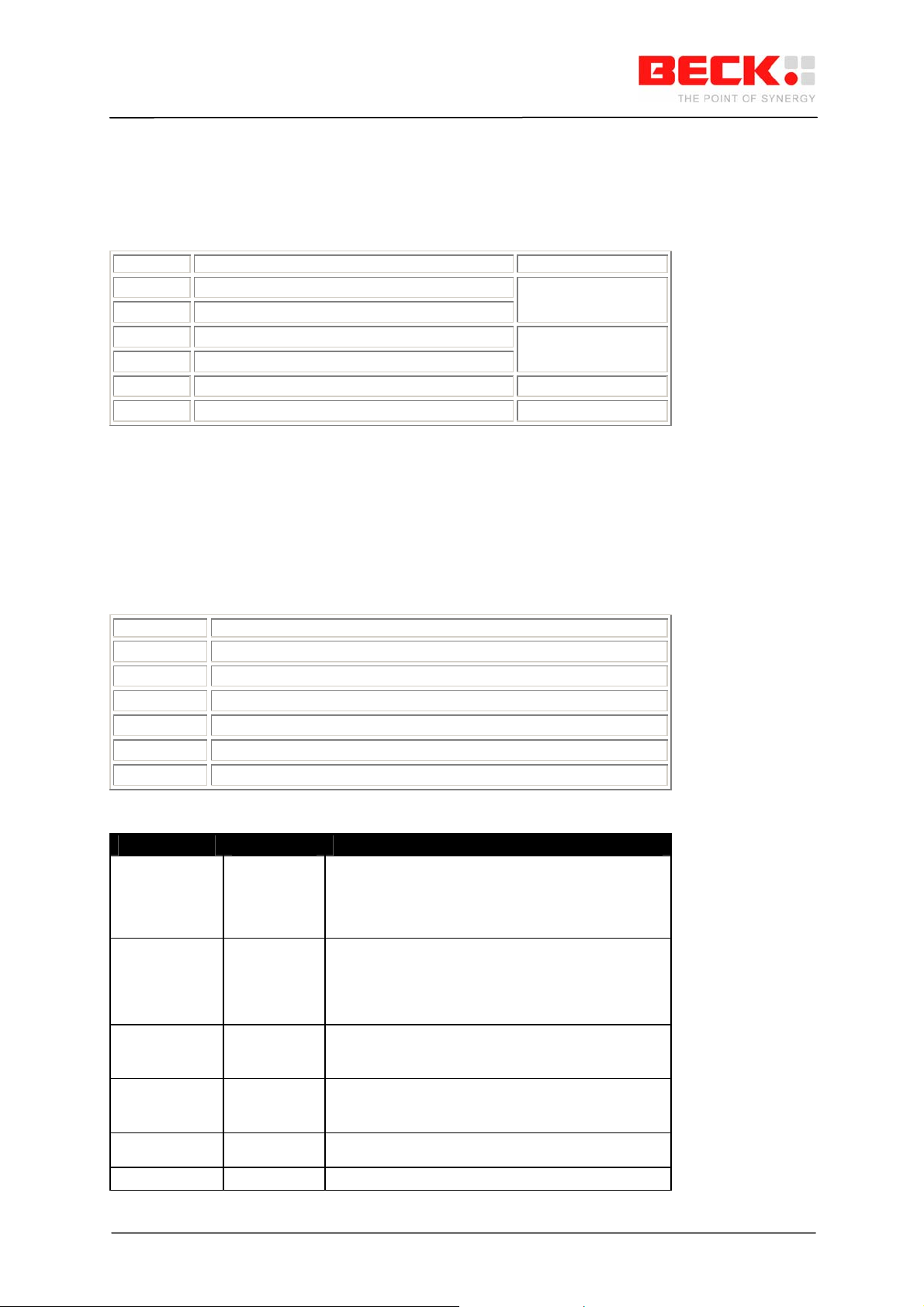
4.17 S42 - DCD, DTR, DSR Connector
This pin header is required for modem connections at COM2. With two jumpers it can connect pins 1,
4 and 6 (DCD, DTR, DSR) of the DSUB plug ST14 (COM2).
Pin assignment (1x6 pin header, 2.54mm pitch):
Pin No. Name
1 DCD (can be bridged via jumper with DTR)
2 DTR (can be bridged via jumper with DCD)
3 DTR (can be bridged via jumper with DSR)
4 DSR (can be bridged via jumper with DTR)
5 NC
6 NC
4.18 S3 - Serial interface COM3 / SPI
] Jumper
] Jumper
Asynchronous serial interface and synchronous serial interface with TTL signal level. The COM3
interface can also be used alternatively as an SPI interface or as a PIO function.
4.7k Ohm pull-up resistors at SDO and SDI enable the SPI interface to run in slave mode.
Pin assignment (1x3 pin header, pitch 2.54mm)
Pin No. Name
1 VCC
2 GND
3 TXD3/SDO/P27
4 RXD3/SDI/P28
5 CTS3/SEL/P18
6 RTS3/SCK/P19
Signal descriptions:
Signal name Direction Description
TXD3
P27
SDO
RXD3
P28
SDI
CTS3
P18
SEL
RTS3
P19
SCK
VCC 3.3 power supply
GND GND, Signal reference
Output
Bi-directional
Output
Input
Bi-directional
Input
Input
Bi-directional
Output
Output
Bi-directional
Output
Serial data Transmit line. TTL level
PIO27
SDO (serial data out)
SC23 as SPI master: MOSI
SC23 as SPI slave: MISO
Serial data Receive line. TTL level
PIO28
SDI (serial data in)
SC23 as SPI master: MISO
SC23 as SPI slave: MOSI
Handshake line. Clear To Send. TTL level
PIO18
Device Select
Handshake line. Request To Send. TTL level
PIO19
SPI clock
(e.g. for externally connected level converter)
©2000-2008 Beck IPC GmbH Page 16 of 24
Page 17
IPC@CHIP DB54
Hardware Manual V1.1 [04.10.2007]
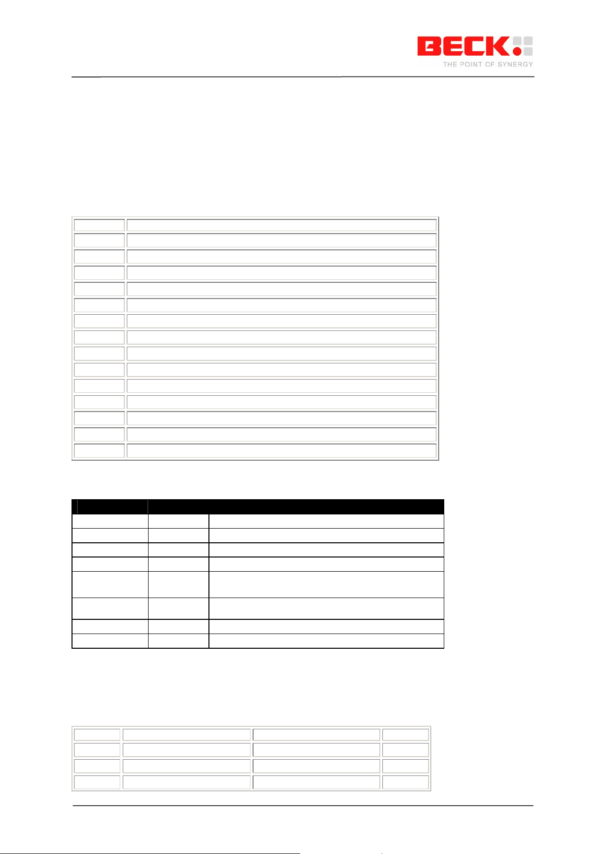
4.19 ST1 - SD/MMC interface
The SD/MMC interface uses the SPI interface of the SC23.
As several devices can be connected to the SPI interface, a PIO signal is required as a device-select
signal (SPI slave select, SEL) for each SPI device. The device-select signals are configured via the
software. PIO18 is reserved as the device-select signal for the SD/MMC interface on the DB54. The
appropriate MMC/SD driver must be installed in order to use the SD/MMC interface. This driver can be
obtained from the BECK IPC GmbH website.
Pin assignment of the SD/MMC connector:
Pin No. Name
1 SLVSEL# (CTS3/PIO18)
2 SDO (TXD3/PIO27)
3 GND
4 +3,3V
5 SCK (RTS3/PIO19)
6 GND
7 SDI (RXD3/PIO28)
8 GND
9 NC
10 WP (PIO10)
11 CD (PIO11)
12 COMMON (GND)
13 GND (shield)
14 NC
Signal descriptions of the SD/MMC interface:
Signal name Direction Description
SDO Output Serial synchronous data output
SDI Input Serial synchronous data input
SLVSEL# Output SPI Slave Select
SCK Output SPI clock
CD (PIO11) Input Card Detect: 0 = Card present
1 = Card not present
WP (PIO10) Input Write Protect: 0 = unlocked
1 = locked
VCC 3.3V power supply
GND GND, Signal reference
4.20 ST4 - PIO Jumper array
This jumper array is used to disable DB54 functions if the corresponding PIO should be used for other
purposes.
Pin assignment (2x8 pin header, pitch 2.54mm)
Pin No. Name Description Pin No.
1 PIO12 (CTS1) WLAN_SELECT# 2
3 PIO2 (INT1) WLAN_RESET 4
5 PIO1 (TMROUT1 / INT3) LED (at ST3 Ethernet Jack) 6
©2000-2008 Beck IPC GmbH Page 17 of 24
Page 18
IPC@CHIP DB54
Hardware Manual V1.1 [04.10.2007]
7 PIO0 (TMRIN1 / INT5#) WLAN_INT# 8
9 PIO10 (TMROUT0) SD/MMC_WP 10
11 PIO11 (TMRIN0) SD/MMC_CD 12
13 NC NC 14
15 NC NC 16
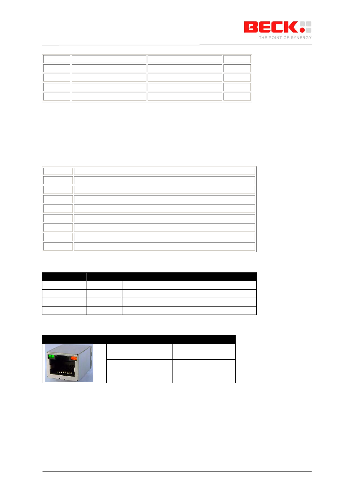
4.21 ST3 - Ethernet Interface
10/100 Base-T Ethernet interface
Activity of the Ethernet interface is indicated by the orange LEDs that are lit up by the SC23. The other
green LED is connected to a PIO of the SC23 and is freely programmable.
Assignment of the RJ45 Ethernet connector:
Pin No. Name
1 TPTX+
2 TPTX3 TPRX+
4 NC
5 NC
6 TPRX7 NC
8 NC
Signal descriptions of the Ethernet interface:
Signal name Direction Description
TPTX+ Output Differential 10/100 Base T transmit signal from SC23
TPTX- Output Differential 10/ 100 Base T transmit signal from SC23
TPRX+ Input Differential 10/100 Base T receive signal from SC23
TPRX- Input Differential 10/100 Base T receive signal from SC23
Ethernet Jack with integrated LED’s:
RJ45 Ethernet Jack LED Description
green LED
TMROUT0/PIO1
(right side)
Activity Status
orange LED
(left side)
On: activity
Off: no activity
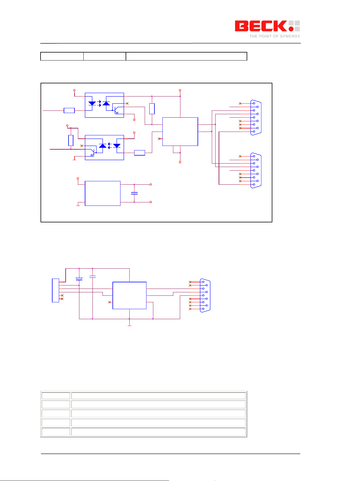
4.22 S6 - CAN0 Interface
The CAN0 interface is equipped with a CAN transceiver module and is not isolated. A 120-Oh m
terminating resistor (R22) is provided between the CANLOW and CANHIGH si gnal (DSUB 9 female).
Additionally it is possible to connect the power supply to pin 9 of the DSUB connector S6 by placing a
0 Ohm resistor at R10. #
©2000-2008 Beck IPC GmbH Page 18 of 24
Page 19
IPC@CHIP DB54
Hardware Manual V1.1 [04.10.2007]
Pin assignment (2x8 pin header, pitch 2.54mm)
Pin No. Name
1 NC
2 CANLOW
3 GND
4 NC
5 CAN_SHLD
6 NC
7 CANHIGH
8 NC
9 NC
Signal descriptions of the CAN interface:
Signal name Direction Description
CAN_LOW Bi-directional Differential CAN Signal
CAN_HIGH Bi-directional Differential CAN signal
CAN_SHLD Shielding of the CAN socket
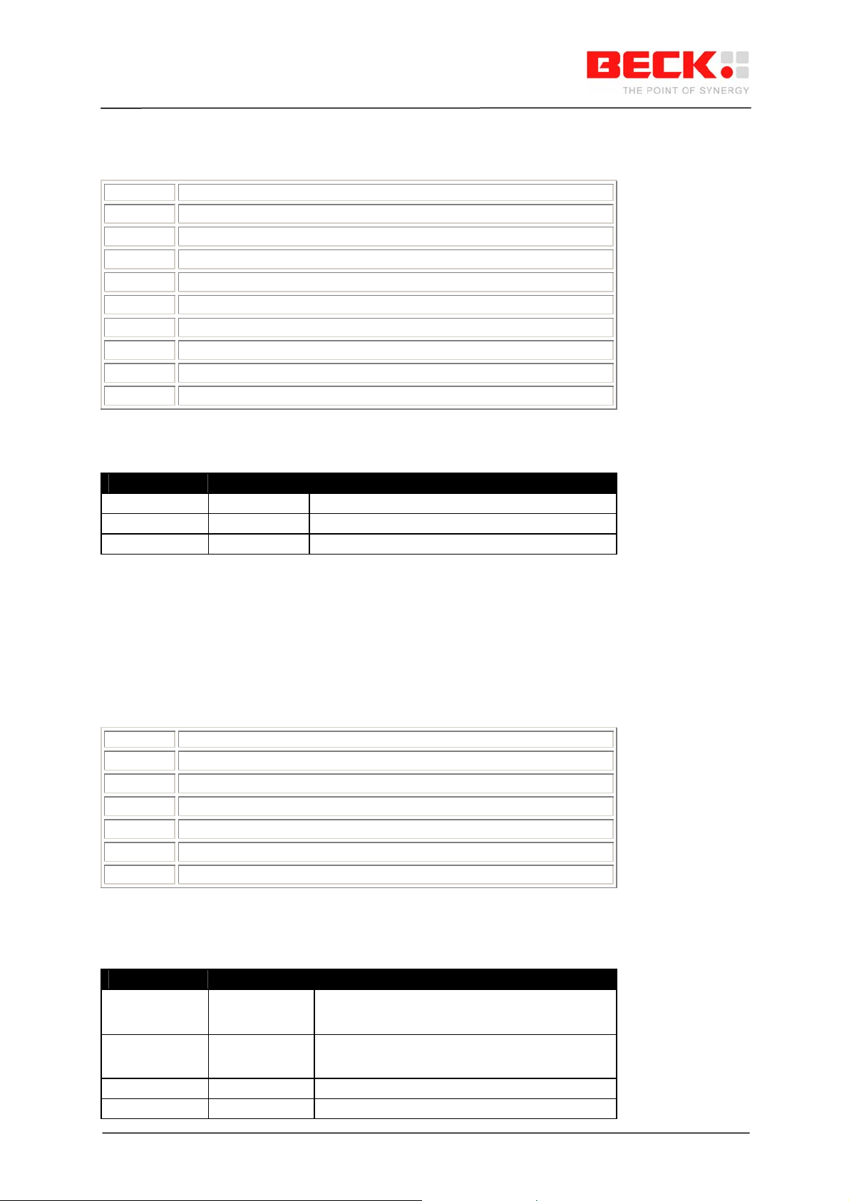
4.23 S38 - CAN1 (COM2) Interface
The second CAN interface is not provided with a CAN transceiver. 3.3 V and 5V are provided on the
pin header for expansion with a CAN transceiver. Alternatively, the signal lines of the CAN1 interface
can also be used as PIO functions. The CAN1TX and CAN1RX signals are shared with the si gnals
RTS2 and CTS2.
Pin assignment (pin header 6-pole, pitch 2.54mm):
Pin No. Name
1 VCC
2 GND
3 CAN1T (CTS2/PIO20)
4 CAN1R (RTS2/PIO21)
5 NC
6 5V
Signal descriptions of the CAN interface:
Signal name Direction Description
CAN_TXD
PIO20
CTS2
CAN_HIGH
PIO21
RTS2
VCC 3.3V power supply for external expansions
5V 5V power supply for external expansions
©2000-2008 Beck IPC GmbH Page 19 of 24
Bi-directional
Bi-directional
Input
Bi-directional
Bi-directional
Output
Differential CAN signal
PIO20
Handshake signal. Clear To Send. TTL level
Differential CAN signal
PIO21
Handshake signal. Request To Send. TTL level
Page 20
IPC@CHIP DB54
Hardware Manual V1.1 [04.10.2007]
GND Signal reference
Example of galvanic isolation of the CAN interface:
CAN_TXD
CAN_RXD
VCC
2 8
R28
390R
3
VCC
R7
8
1k
7
6
5
GND
VCC
1
+Vin
+5V +5V
2 4
-Vin -Vout
GND
DC/DC converter
U20
6N135
6N135
+Vout
ISO2
ISO1
7
6
5
CAN_GND
CAN_VCC
2
3
6
R15
390R
C16
100n
CAN_VCC
CAN_GND
CAN_VCC
R19
1k
1 7
TXD
4 6
RXD
5
REF
RS
8
CAN_GND
Example of the CAN interface without galvanic isolation:
P2
1
CAN_GND
6
2
3
IC1
CANH
CANL
GND VCC
82C250
2
CAN_SHLD
CAN_GND
CAN_GND
CAN_GND
7
3
8
4
9
5
1
6
2
7
3
8
4
9
5
CAN
D-SUB-9f
P1
CAN
D-SUB-9m
P2
1
6
2
7
3
8
4
9
5
D-SUB-9f
CAN
3V3
GND
CANTX
CANRX
NC
5V
CAN1
1
2
3
4
5
6
S38
+
C2
10uF
C1
IC1
100uF
1
TXD
4
RXD
5 8
REF RS
SN65HVD231
GND
CANL
CANH
GND VCC
2 3
CANH
7
CAN_GND
CANL
6
4.24 ST16 & ST13 - USB Interface
The USB interface of the DB54 has the ability to work in host or device mode. A software driver is
needed to use the USB, which can be obtained from the BECK IPC GmbH website. It is not possible
to operate the USB in host mode and device mode at the same time.
ST16 USB host Pin assignment (USB-A connector)
Pin No. Name
1 5V
2 USBN
3 USBP
4 GND
©2000-2008 Beck IPC GmbH Page 20 of 24
Page 21
IPC@CHIP DB54
Hardware Manual V1.1 [04.10.2007]
Signal descriptions of the USB host interface:
Signal name Direction Description
USBN Bi-directional Differential USB signal
USBP Bi-directional Differential USB signal
5V 5V (max. 500mA) power supply for devices
connected to the USB host interface.
GND Signal reference
The external USB voltage can be taken from pin header S39 pin 4
ST13 USB device pin assignment (USB-B mini connector)
Pin No. Name
1 VCC_USB_DEVICE (connected to S39 pin 4)
2 USBN
3 USBP
4 AB_DETECTION
5 GND
Signal descriptions of the USB device interface:
Signal name Direction Description
USBN Bi-directional Differential USB signal
USBP Bi-directional Differential USB signal
AB_DETECTION Not connected
VCC_USB_DEVICE USB voltage input
GND Signal reference
©2000-2008 Beck IPC GmbH Page 21 of 24
Page 22

IPC@CHIP DB54
Hardware Manual V1.1 [04.10.2007]
5. Technical dat a
5.1 Climatic data
Storage temperature: -25°...+70° C
Operational ambient temperatures: 0°....55° C
5.2 Mechanical data
DB54 board module dimensions (H x L x D): 31mm x 135mm x 195mm (+/-1 mm)
5.3 Electromagnetic data
This product is a development board without the CE mark.
5.4 Electrical data
Input voltage: 9…30 VDC
Current consumption (DB54 without expansions): max. 1.7 W
©2000-2008 Beck IPC GmbH Page 22 of 24
Page 23

IPC@CHIP DB54
Hardware Manual V1.1 [04.10.2007]
6. General conditions of use
6.1 Scope of application
Use of the DB54 Development Board or DK55 Devel opment Kit is permissible exclusive ly in accordance with the
terms and conditions stated below. These terms and conditions of use shall be deemed as accepte d with the
commissioning of the development board.
7. Exclusion of warranty and liability
This product is a development board without the CE mark. The board must therefore only be used for
hardware/software development. Use of the development board outside the specified environment is the
responsibility of the user and shall be carried out at his or her own risk, exempting Beck from any liability.
Claims by the user for compensation against Beck in conjunction with the use of this product shall be excluded.
Insofar that information, hardware, software and documentation is transferred without charge, liability is excl uded
for any material defects and deficiencies in title of the information, hardware, software and documentation, in
particular for their correctness or absence of errors, completeness and/or usability.
©2000-2008 Beck IPC GmbH Page 23 of 24
Page 24

IPC@CHIP DB54
Hardware Manual V1.1 [04.10.2007]
8. History
Rev. Date Author Comments
0.90 xx.xx.2007 S. Perzborn Initial preliminary revision
1.00 04.10.2007 S.Perzborn First version
1.10 24.04.2008 S.Perzborn correction of the SPI Pin header name (chapter 4.18) correction
©2000-2008 BECK IPC GmbH All rights reserved. No part of
this document may be copied or reproduced in any form or by
any means without the prior written consent of BECK IPC
GmbH. The information in this document is subject to change
without notice. Devices sold by BECK IPC GmbH are covered
by warranty and patent indemnification provisions, which are
given in the BECK IPC GmbH Terms and Conditions of Sale
only.
BECK IPC GmbH MAKES NO WARRANTY, EXPRESS,
STATUTORY, IMPLIED OR BY DESCRIPTION, REGARDING
THE INFORMATION SET FORTH HEREIN OR REGARDING
THE FREEDOM OF THE DESCRIBED DEVICES FROM
INTELLECTUAL PROPERTY INFRINGEMENT. BECK IPC
GmbH MAKES NO WARRANTY OF MERCHANTABILITY OR
SUITABILITY FOR ANY PURPOSE.
BECK IPC GmbH shall not be responsible for any errors that
may appear in this document. BECK IPC GmbH makes no
commitment to update or keep current the information
contained in this document.
Life critical applications - BECK products are not authorised for
use as critical components in life-support devices or systems
unless a specific written agreement pertaining to such intended
use is executed between the customer and BECK prior to use.
Life-support devices or systems are those, which are intended for
surgical implantation in the body, or which sustain life, and whose
failure to perform, when properly used in accordance with
instructions for use provided in the Operation Manual, can be
reasonably expected to result in significant injury to the user.
BECK IPC GmbH customers using or selling these products for
use in such applications do so at their own risk and agree to fully
indemnify BECK IPC GmbH for any damages resulting from such
application.
Right to make changes - Beck IPC GmbH reserves the right to
make changes without notice in the products, including software,
described or contained herein in order to improve design and/or
performance. Beck IPC GmbH assumes no responsibility or
liability for the use of any of these products.
©2000-2008 Beck IPC GmbH Page 24 of 24
 Loading...