

Page 1

X23(RU)
service manual
Page 2

Catalog
Chapter One About Maintenance
1.1 Safety precautions
1.1.1 Precautions for antistatic
1.1.2 About placement position
1.2 Maintenance method
1.2.1 Visualized method
1.2.2 Electric resistance method
1.2.3 Voltage method
1.2.4 Current method
1.2.5 Cutting method
1.2.6 Element substitution method
1.2.7 Comparison method
1.3 Required device for maintenance
Chapter Two Functions and Operation Instructions
1
1
1
1
1
1
2
2
2
2
2
2
3
4
2.1 USAGE INTRODUCTION
2.1.1 FUNCTIONS AND FEATURES
2.1.2 BUTTONS AND JACKS ILLUSTRATION
2.1.3 MAIN MENU ILLUSTRATION
2.1.4 PLAYING INTERFACE ILLUSTRATION
2.1.5 TUNING INTERFACE ILLUSTRATION
2.1.6 RECORDING INTERFACE ILLUSTRATION
2.2 BASIC OPERATIONl
2.2.1 INSTALL USB DRIVE PROGRAM
2.2.2 USE MOBILE STORAGE FUNCTION
2.2.3 DISCONNECT USB SAFELY
2.2.4 BROWSE/CANCEL FILE
2.2.5 PLAY MUSIC
2.2.6 A-B REPEAT FUNCTION
2.2.7 RECORDING
4
4
4
5
5
6
6
6
6
6
6
6
7
7
7
Page 3

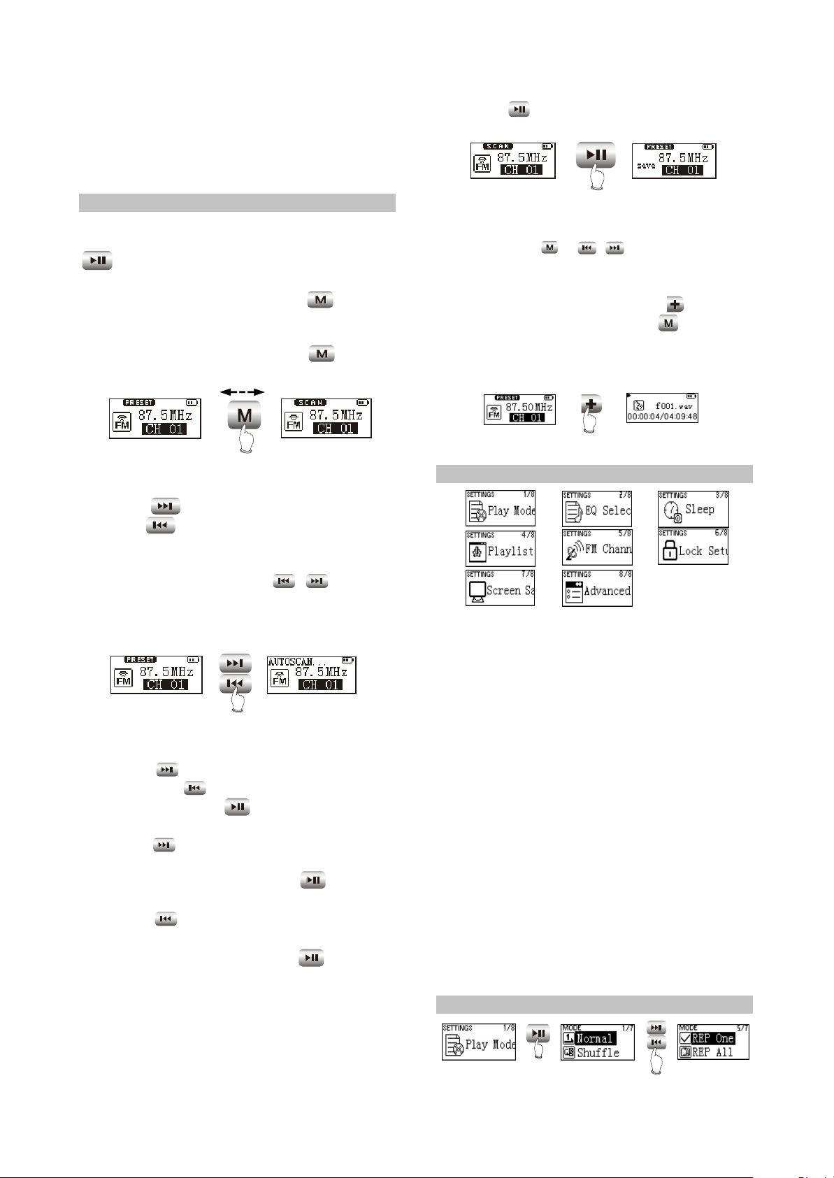
2.2.8 TUNING
8
2.3 SETTINGS
2.3.1 SETTINGS
2.3.2 PLAY MODE
2.3.3 EQ SELECT
2.3.4 SLEEP
2.3.5 PLAYLIST
2.3.6 FM CHANNEL
2.3.7 LOCK SETUP
2.3.8 SCREEN SAVE
2.3.9 ADVANCED
2.3.10 ADVANCED
2.4 SSPECIFICATION
Chapter Three Principle and Servicing
section One Principle of the Player
8
8
8
9
9
9
9
9
10
10
10
11
12
12
3.1.1 Function introduction
3.1.2 Block diagram of the player
3.1.3 Introduction to IC of the player
Section Two Unit Circuit Principle
3.2.1 FLASH circuit
3.2.2 FM tuning circuit
3.2.3 OLED module circuit
3.2.4 USB jack circuit
3.2.5 Button circuit
3.2.6 Headphone jack circuit
3.2.7 Power on/off control circuit
3.2.8 Reset circuit
3.2.9 MIC circuit
3.2.10 Low voltage detecting circuit
Section Three Servicing Cases
12
12
13
14
14
15
16
17
18
18
19
20
20
21
22
3.3.1 Servicing cases
3.3.2 Troubleshooting flow chart
Section Four Waveform diagram
22
26
31
Page 4

Section Five Function Introduction to IC
38
3.5.1 Function introduction to PNX0101ET
3.5.2 Function introduction to K9F2G08U0M
3.5.3 Function introduction to TCM809ZVBN713
3.5.4 Function introduction to PQ1X281M2ZP
3.5.5 Function introduction to Si1912
3.5.6 Function introduction to Lm2713
3.5.7 Function introduction to TEA5767HN
Chapter Four Disassembly and Assembly Process
4.1 Disassembly process of the player
4.2 Assembly process of the player
4.3 Disassembly and assembly process for OLED screen
4.4 Disassembly and assembly process for USB jack
Chapter Cinque PCB board & Circuit diagram
38
49
51
52
53
53
54
57
57
59
59
59
60
Section One PCB board
Section Two circuit diagram
Chapter six BOM List
60
62
65
Page 5

Chapter One About Maintenance
1.1 Safety precautions
1.1.1 Precautions for antistatic
Movement and friction will both bring static electricity which causes serious damages to integrated
IC. Though static charge is little, when a limited quantity of electric charge is added to large-
scaleintegrated IC, as the capacitance is very small in the meantime, now the integrated IC is very much
easy to be struck through by static electricity or the performance will decrease. Thus static electricity
prevention is of extraordinary importance. The following are several measures to prevent static
electricity:
1. Use a piece of electric conduction metal with the length of about 2 metres to insert into the earth,
and Fetch the lead wire from the top of the surplus metal and connect to the required static electricity
device. The length and depth of the metal embedded under the earth should be determined according to
the wettability of the local soil. For humid places, it may be shorter, and longer and deeper for dry places.
If possible, it can be distributed and layed in terms of “#” shape.
2. On operating table-board, the antistatic table cushion should be covered and grounded.
3. All devices and equipments should be placed on the antistatic table cushion and grounded.
4. Maintenance personnel should wear antistatic wrist ring which should be grounded.
5. Places around the operating position should also be covered with electric conduction cushion or
Painted with antistatic paint.
1.1.2 About placement position
1. Audio power amplifier cannot be installed in places with high temperature and humidity.
2. Positions for placement should be stable and secure.
1.2 Maintenance method
1.2.1 Visualized method
Directly view whether abnormalities of collision, lack of element, joint welding, shedding welding,
rosin joint, copper foil turning up, lead wire disconnection and elements burning up among pins of
- 1 -
Page 6

Elements appear. Check power supply of the machine and then use hands to touch the casing of part of
elements and check whether they are hot to judge the trouble spot. You should pay more attention when
using this method to check in high voltage parts.
1.2.2 Electric resistance method
Set the multimeter in resistance position and test whether the numerical value of resistance of each
point in the circuit has difference from the normal value to judge the trouble spot. But in the circuit the
tested numerical value of resistance is not accurate, and the tested numerical value of integrated IC's
pins can only be used for reference, so the elements should be broken down for test.
1.2.3 Voltage method
Voltage method is relatively convenient, quick and accurate. Set the multimeter in voltage position
and test power supply voltage of the player and voltage of a certain point to judge the trouble spot
according to the tested voltage variation.
1.2.4 Current method
Set the multimeter in current position and test current of the player of a certain point to judge the
trouble spot. But when testing in current method, the multimeter should be series connected in the
circuit, which makes this method too trivial and troublesome, so it is less frequently used in reality.
1.2.5 Cutting method
Cutting method should be combined with electric resistance method and voltage method to use.
This method is mainly used in phenomena of short circuit and current leakage of the circuit. When
cutting the input terminal voltage of a certain level, if voltage of the player rises again, it means that the
trouble lies in this level.
1.2.6 Element substitution method
When some elements cannot be judged good or bad, substitution method may de adopted directly.
1.2.7 Comparison method
A same good PC board is usually used to test the correct voltage and waveform. Compared these
data with those tested through fault PC board, the cause of troubles may be found.
Through the above maintenance method, theoretical knowledge and maintenance experience, all
difficulties and troubles will be readily solved.
- 2 -
Page 7

1.3 Required device for maintenance
Audio Generator
Digital oscillograph ( 100MHE)
SMD rework station
Multimeter
Soldering iron
Pointed-month pincers
Cutting nippers
Forceps
Electric screw driver
Terminals connecting cord
Headphone
Microphone
- 3 -
Page 8
Chapter Two
Functions and Operation Instructions
2.1 USAGE INTRODUCTION
2.1.1 FUNCTIONS AND FEATURES
#Philips PNX0101 audio decode chip
Adopt famous Plilips PNX0101 audio decode chip, special for Hi-Fi MP3 player, forcefully making
up audio signal loss when compressing MP3 to revert audio signal better.
#Play MP3/WMA/WAV files
Support 16kbps ~ 320kbps MP3 file and 8kbps ~ 192kbps WMA file.
#Mobile storage function
Capable of downloading files from Windows resource manager.
#FM tuning
Full-auto, automanual and manual scanning function may listen to FM radio station program more
easily.
#Voice recording function
May be used to record in class, meeting and interview.
#USB 2.0 transmission (full speed)
USB2.0 full speed data transmission.
#Support firmware upgrading function
Support upgrading function. You may add new function to the built-in program of this player
conveniently.
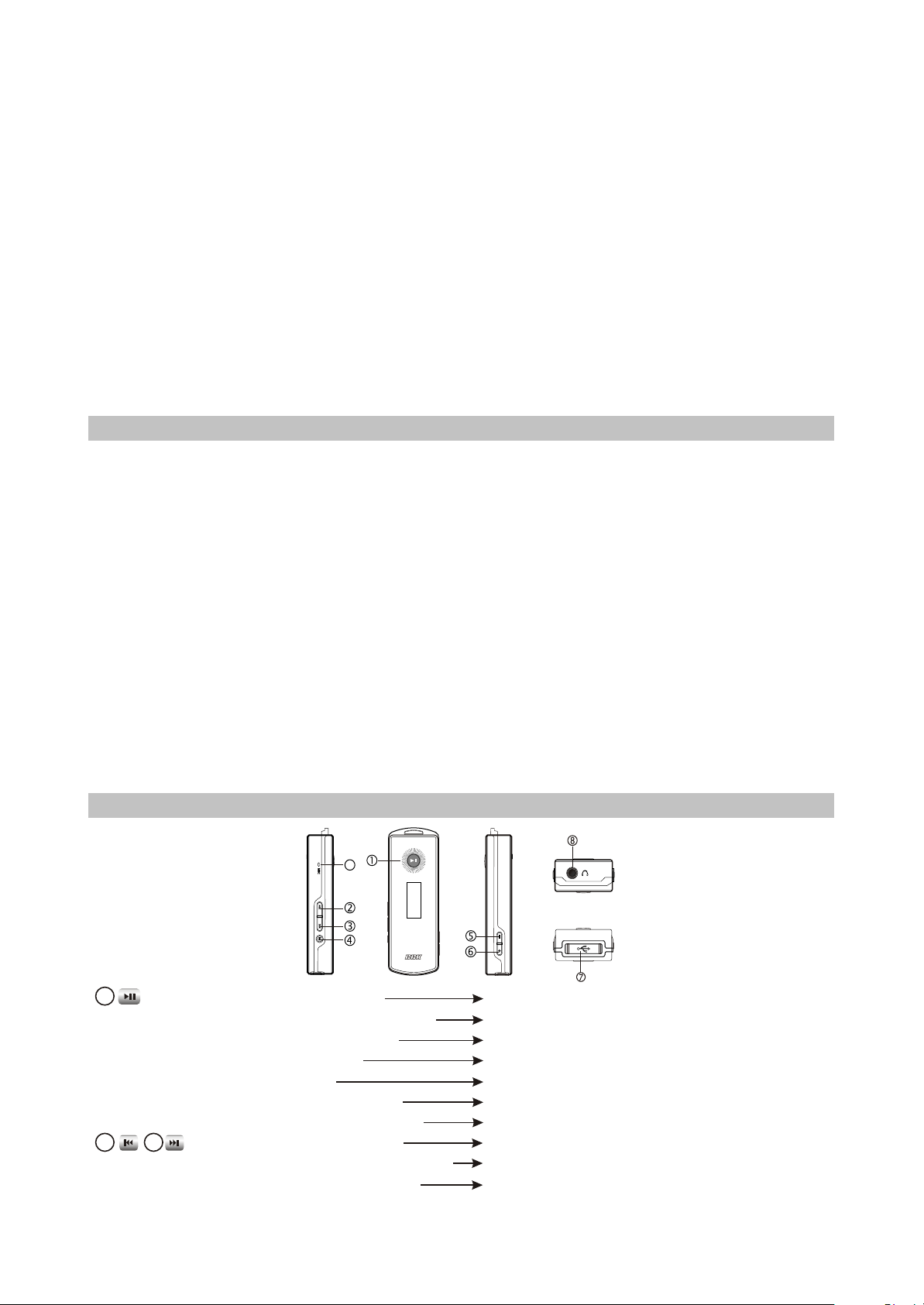
2.1.2 BUTTONS AND JACKS ILLUSTRATION
9
1
2
#Press in power off mode
#Press for long in power on mode
#Press in playback interface
#Press when recording
#press when tuning
#press in tuning SCAN mode
#press when operating in menu
3
#Press in playback interface
#Press for long in playback interface
#Press in tuning PRESET mode
power on
power off
switch in pause/play
pause recording
mute
save radio station and switch mode to PRESET
enter selected item or confirm setup
the previous/next track
fast backward/forward
select channel
- 4 -
Page 9
#Press for long in tuning PRESET mode
#Press in tuning SCAN mode
#Press for long in tuning SCAN mode
#When operating in menu
#Press or for long in “My EQ”
M
4
#Press for long in any mode
#Press when tuning
#Press for long when recording
#Press when operating in menu
5
6
Press when playing
#
#Press in playback interface or when tuning
#Press in "My EQ"
#Press "-" button when browsing file
#Press "+" button for long when tuning
7
USB jack
8
Headphone jack
9
MIC: microphone
2.1.3 MAIN MENU ILLUSTRATION
full auto scanning
manual scanning
automanual scanning
move cursor or set item
select the frequency point you want
to set
enter main menu
switch in PRESET and SCAN mode
quit recording
not save the setup and return to the
previous menu
Set A-B reread
adjust volume
adjust dB value
enter cancelling file dialogue box
enter FM recording
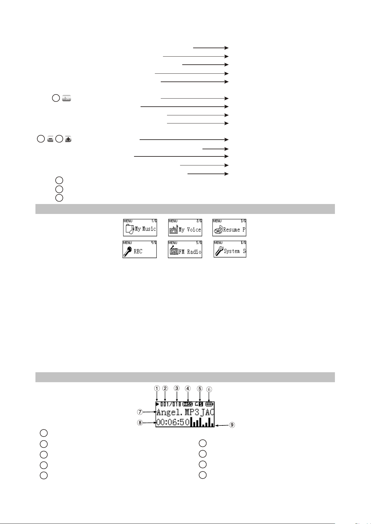
#My music
Memorize music file.
#My Voice
Memorize microphone recording file, such as meeting, classroom and interview recording, etc.
#Resume Play
Select "Resume Play" and the player begins to play from the position that music stopped playing
ast time.
#REC
Select "REC"to enter recording mode.
#FM Radio
Select " FM Radio"to enter radio setmode.
#System Setup
Select " System Setup" to set system items.
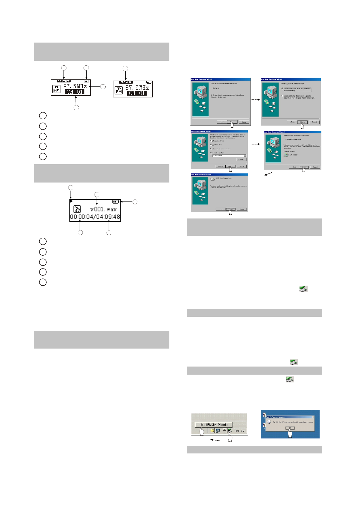
2.1.4 PLAYING INTERFACE ILLUSTRATION
1
Playback state
6
Serial number of the current track
2
Number of all tracks
3
Sound effect mode
4
5
Playback mode
Battery capacity
7
ID3 information/singer/lyrics display
8
Time that has been played of the current track
9
Spectrum of the currenttrack
- 5 -
Page 10
2.1.5 TUNING INTERFACE
ILLUSTRATION
1
1
PRESET mode (normal receiving)
Battery capacity
2
Frequency of the current radio station
3
4
PRESET channel display
5
SCAN mode (scanning)
2
3
4
5
2.1.6 RECORDING INTERFACE
ILLUSTRATION
5
1
3. After installation finishes, restart the computer
and you may use the mobile storage function
normally.
Shown as the following figure:
2
3
1
Name of recorded file
Battery capacity
2
Time that has been recorded
3
4
The left recordable time
5
Recording state
4
As for the name of recorded file"V001.WAV":
001 is serial number of the current recorded
track and arranged according to sequence; WAV
is file format after recording.
2.2 BASIC OPERATION
2.2.1 INSTALL USB DRIVE
PROGRAM
If your computer is Windows 98, you must
install drive program if you want to use the
mobile storage function of MP3 player in
computer.
1. Place USB drive disc into CD-ROM driver of
computer.
2. Connect MP3 player to computer, and the
computer will automatically indicate that new
firmware device has been found, and run the
installation guide, shown as the following
figure. You only need to find the drive
information file on disc according to prompt
information to finish the installation of drive
program.
2.2.2 USE MOBILE STORAGE
FUNCTION
This player can be used as mobile storage
in Windows ME/2000/XP operating system. In
Windows 98SE and Mac operating system, drive
program must be installed firstly and then used
as mobile storage.Connect MP3 PLAYER and
computer with USB transmission line. After the
bottom right corner of desktop appears “ ”
symbol, the mobile storage function of Mp3
PLAYER may be used normally.
NOTE:
#To avoid abnormality of the player appears, you
are suggested to power off firstly before
connecting MP3 PLAYER with computer, and
then use USB transmission line to connect
MP3 PLAYER, then connect computer.
#In Windows 98 system, there is no “ ”symbol.
2.2.3 DISCONNECT USB SAFELY
After operation finishes, click " " symbol
on bottom right corner of Windows desktop with
right button of mouse, and disconnect USB
safely according to the computer prompt.
2.2.4 BROWSE/CANCEL FILE
#BROWSE FILE
- 6 -
Page 11
In any case, press button for long to
enter "Main Menu". Music fileand recording file
are separately saved in the first two items of
main menu, "My Music" and "My Voice". Press
/
button to select upward or downward
and then press button to enter files browsing.
are only for the current track. After fast
backward/forward to the beginning/ending of
track, it switches into normal playback
automatically
#ADJUST VOLUME
PRESS
FOR LONG
PRESS
PRESS
display of adjusting volume in music playback
#CANCEL FILE
interface is shown as follows:
When browsing files, press button and
the cancel dialogue box will pop up.
Press button to select "YES" and
/
then press button to cancel the file.
Select "NO" or press button to exit.
#Music playback will be paused when browsing
PRESS
PRESS
#In some operating system (such as complex
2.2.5 PLAY MUSIC
#PLAY MUSIC
Press button to select song In
"My Music". Press button or select
playback in main menu to begin playing music,
meanwhile the playback interface displays.
#PAUSE PLAYING MUSIC
When playing, press button to switch to
pause state. Press button again to
continue playing.
#NEXT and PREV
When playing, pressing button may skip
to the next track to play. If playback time of the
current track is less than 5 seconds, pressing
button may skip to the previous track to play,
otherwise the current track will be played again if
playback time is more than 5 seconds.
#3FF and FB
When playing, pressing button for long
may realize fast forward.
/
pressing buttons may probably has slow
response or has no lyrics display. When playing
some non standard songs or songs with special
format, noise may probably occur.
certain segment repeatedly, please use A-B
repeat function.Press button for the first time
to select the beginning point that you desire
PRESS
to repeat play and screen displays " ";press it
for the second time to select the ending
point that you desire to repeat play and screen
displays " “, and system begins to repeat
play between A-B segment. Press button for
the third time to cancel repeat and
continue to play.
and press button for long to exit recording
PRESS
FOR LONG
and then make files.
.
CAUTION:
Fast forward and fast backward operation
When playing or tuning or tuning, pressing
button or for long way adjust volume. The
/
CAUTION:
file.
font Windows), the operation of copying
lyrics/song file and changing song's name may
probably lead to incorrect display.
When playing WMA songs of VBR ,
2.2.6 A-B REPEAT FUNCTION
When playing, if you want to listen to a
PRESS PRESS PRESS
2.2.7 RECORDING
When recording, press button to pause
When playing, pressing button for long
may realize fast backward.
PRESS
FOR LONG
PRESS
PRESS
FOR LONG
CAUTION:#To avoid sudden power-off
when recording, you cannot record when in low
battery and when disc is fully written.
- 7 -
Page 12
If you are recording, it indicates "FULL
DISC" and exits recording.
#When recording with microphone, if you press
buttons and the sound of pressing may
probably be recorded.
2.2.8 TUNING
#ENTER TUNING MODE
Select "FM Radio" in main menu and press
button to listen to radio.
#EXIT TUNING MODE
When listening to radio, press button
for long to return to main menu.
#PRESET/SCAN MODE SWITCH
When listening to radio, press button
to switch between PRESET and SCAN mode.
PRESS
1. PRESET mode
#ADJUST CHANNEL
Press button to enter the next channel,
and press button to enter the
previous channel.
#FULL AUTO SCANNING
In PRESET mode, press button
for long to begin full auto scanning. All
scanned radio stations will be saved in PRESET
channel automatically.
PRESS
FOR LONG
2. SCAN MODE
#MANUAL/AUTOMANUAL SCANNING
Press button to increase 0.1MHz each
time; and press button to decrease 0.1
Mhz each time. Press button to save radio
station.
Press button for long to increase
frequency continuously and stop until radio
station has been searched. Press button to
save radio station.
Press button for long to decrease
frequency continuously and stop until radio
station has been searched. Press button to
save radio station.
#SAVE RADIO STATION
Select channel in PRESET mode firstly, and
then switch to SCAN mode to adjust fre quency
(manually or auto manually). After scanning
desired frequency.
/
press button to save into the current
PRESET channel.
PRESS
CAUTION:
In the course of full auto/automanual
scanning, press or button to stop
/
scanning.
#FM RECORDING
When listening to radio , press button for
long to enter FM recording . Press button for
long to stop recording and generate into
recording file.The generated file of FM recording
is wav format.
PRESS
FOR LONG
2.3 SETTINGS
2.3.1 SETTINGS
#Play Mode
Normal
Shuffle
Playlist
Intro
REP One
REP ALL
REP DIR
#EQ Select
Normal
PURE
POP
Clas
Jazz
Rock
Dbass
Disco
My EQ
#Sleep
Disable~120Min
2.3.2 PLAY MODE
PRESS
#Playlist
Browse
Edit
Delete
#FM Channel
Auto
Mono
#Lock Setup
Lock Disable
Lock Enable
#Screen Save
Disable~5Min
#Advanced
My EQ
REC Set
Format
Load Default
System Info
Language
PRESS
- 8 -
Page 13
The playback symbol displays on playback
interface is shown as follows:
play according to track sequence.
random play any one track.
play the track edited in program list.
browse play each track for 10 seconds.
repeat play single track.
repeat play all tracks.
repeat play all tracks in this Folder.
CAUTION:
#Play mode is defaulted to "Normal" each time
when power on.
#Files in "My Voice" only support sequence
playback.
#When playing files in "My Voice", there is no
"Play mode" item.
2.3.3 EQ SELECT
Press button to enter "EQ SELECT",
and then use to move cursor, shown
/
as follows:
PRESS
The corresponding icons of each EQ mode
in playback mode are shown as follows:
NORMAL
PURE
POP
CLAS
JAZZ
ROCK
DBASS
DISCO
My EQ
Select "MY EQ", and correspond with the
sound effect that you have preset in "MAIN
MENU->SYSTEM SETUP->ADVANCED". If you
have not set it, it defaults "MY EQ" to NORMAL"
sound effect.
When the cursor moves to a certain sound
effect mode, the sound effect mode played by
MP3 player will switch to that in the cursor for the
moment to facilitate you to select your desired
sound effect mode. Press button to confirm
this sound effect mode.
CAUTION:
When playing files in "REC", there is no”EQ
SELECT" item.
2.3.4 SLEEP
Press or button to adjust the
timing power-off time. After setup finishes, press
button to save and then exit, and press
button not to save and then exit. If timing power
off time is 15 minutes, after 15 minutes, MP3
PLAYER will power off automatically.
PRESS
PRESS
CAUTION:
#It is defaulted to be invalid each time when
power on.
#Timing power-on time is a rough time, and may
have difference.
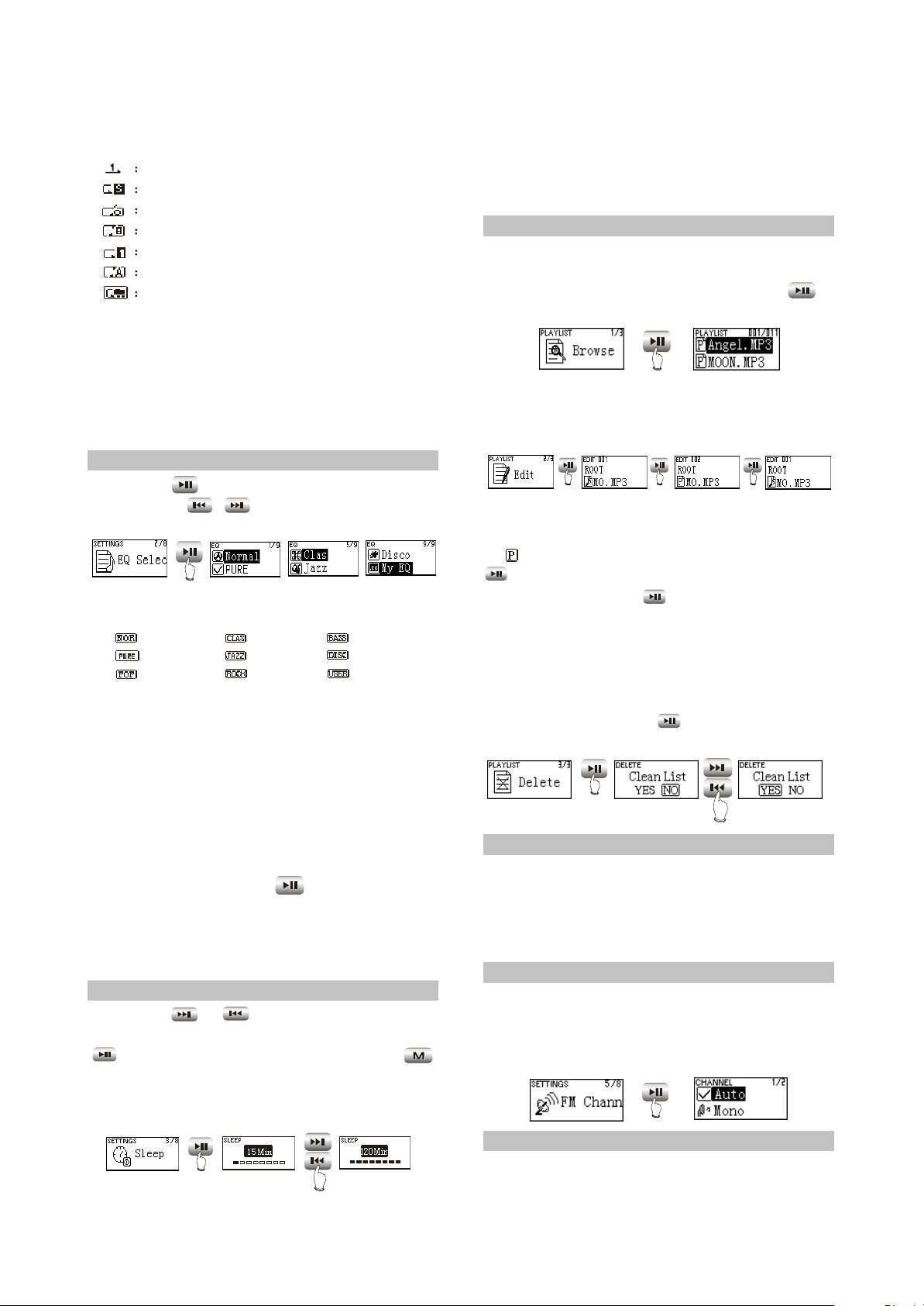
2.3.5 PLAYLIST
Select "Browse" , and you may check how
many songs have been program-med into
playlist. When browsing play list. Pressing
button may begin playing.
PRESS
Note: Playback will be paused when in
"Browse" or "Edit list".
#Edit
PRESS PRESS PRESS
As in the above illustration, enter "Edit" and
browse files.The icon before songs in the playlist
is " ". Select a song not in the playlist and press
button to add it intothe list. Select a song in
the playlist ,and press button to cancel it from
the playlist
You can add 15 songs into the playlist at
most.
#Delete
Select "Delete". After dialogue box pops up,
select "YES", and press button to confirm
and the playlist is cleared.
PRESS
PRESS
NOTE:
#If the operation of adding or cancelling music
files is detected, MP3 PLAYER will clear
the playlist automatically.
#You cannot enter "Edit list" and "Clear list"
when in program playback.
2.3.6 FM CHANNEL
You can select the FM channel in settings.
When select Auto, it changes the channel
automatically. When select Mono, it tunes at
Mono channel all the time.
PRESS
2.3.7 LOCK SETUP
Entering this menu may open or close auto
buttons lock function.
- 9 -
Page 14
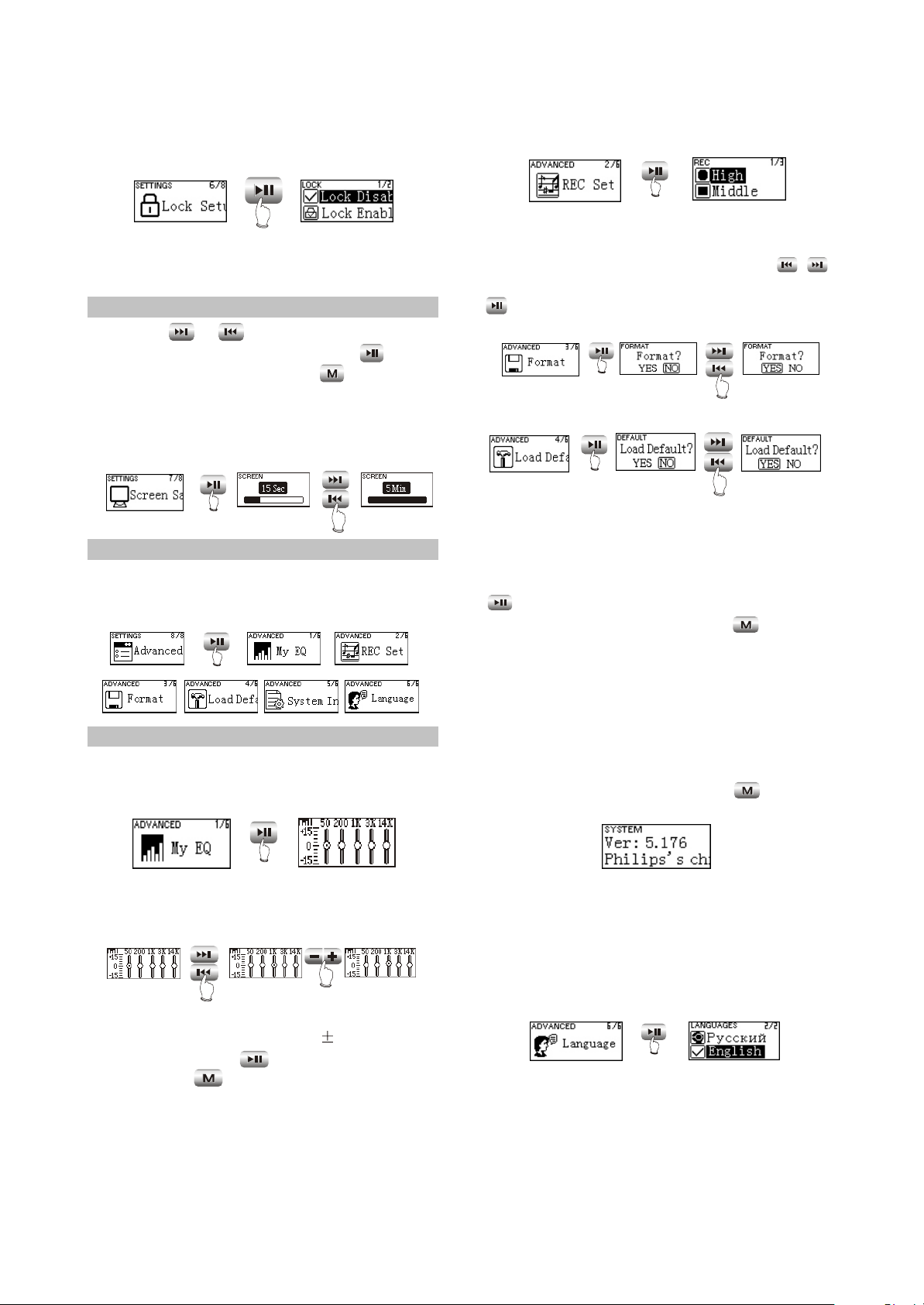
If “Lock Enable” is selected and not any
button is operated during 30 seconds, all button
functions will be locked automatically.
Three kinds of recording quality adopt IMA-
ADPCM format coding.
PRESS
PRESS
CAUTION:
Lock is only effective in playback, recording
and tuning modes.
2.3.8 SCREEN SAVE
Press or button to adjust the screen
saver time. After setup finishes, press button
to save and then exit, and press button not
to save and then exit. If the screen saver setup
time is 3 minutes and no operation occurs within
3 minutes, MP3 PLAYER will enter screen saver
state automatically.
PRESS
PRESS
2.3.9 ADVANCED
Advanced items include some other system
internal setup, such as user sound effect setup,
default setup and system information.
PRESS
2.3.10 ADVANCED
#My EQ
In "My EQ" interface, you may see the
decibel (dB) of each frequency.
#Formatting
Enter this menu, and you may format hard
disk. When dialogue box pops up, press
/
button to move cursor to “YES”, and then press
button to confirm to finish formatting
operation.
PRESS
PRESS
#Default
PRESS
PRESS
If you want to restore MP3 PLAYER to
factory setup state (data and song files cannot
be cancelled), you may select “Load Default”.
After dialogue box pops up, select “YES” , press
button to confirm and then exit to restore to
default state. Select “NO” or press button to
cancel.
CAUTION:
Restore to "Default" state is effective only
when power on again.
#System Info
You may find information of firmware
version, total disc capacity and left disc capacity.
In system information menu, press button to
return to the previous menu.
PRESS
If you want to adjust the decibel of mediant
(1k HZ), operate according to the below
illustration.
PRESS
PRESS
When adjusting width, take 3dB as a step
and the max adjustable range is 15dB. After
setup finishes, press button to confirm and
exit, and press button to exit with the original
setup not being changed.
#REC Set
Here to set the recording quality ,The
recording quality is higher, the sound quality is
better and the used space is more.
CAUTION:
Because firmware will use some space, the
displayed content capacity may probably be
different from the actual capacity.
#Languages
Russian and English are supported.
PRESS
#Upgrade
Download the latest firmware upgrading file
from BBK website firstly, such as "BBK_X23RU.
ebn" and "X23RU_Resource.bin", copy the two
files into MP3 PLAYER at the same time, and
then power on again.
- 10 -
Page 15
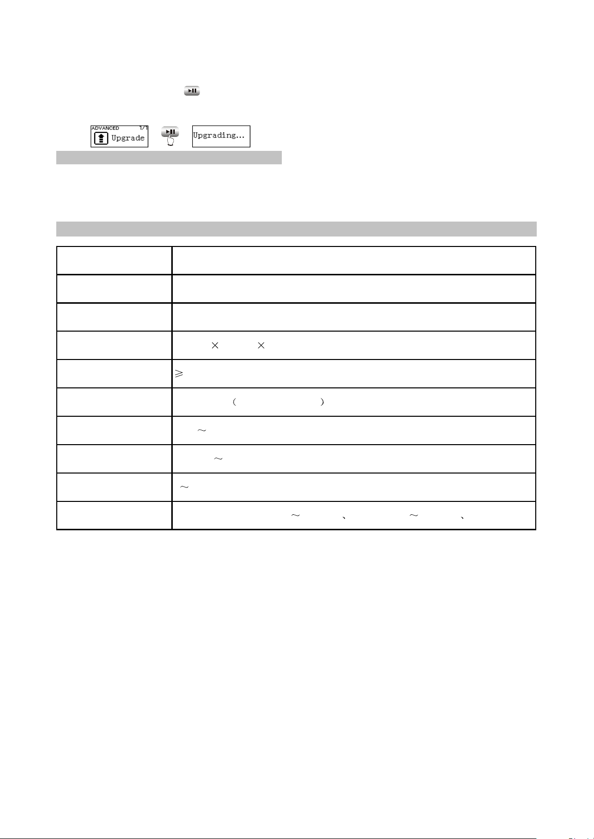
Find "Upgrade" item in "ADVANCED" of
Model
Audio decode chip
Continuous playback
time
Dimensions/weight
Audio SNR
Theadphone ou
Frequency range
FM tuning range
Working temperature
Files supported
90dB
The longest time is about 15 hours
80.2mm 28.5mm 14.5mm about 28.5g(without battery),40g(with battery)
X23
Philips PNX0101
9mW+9mW 32ohm impedance )
18Hz 20kHz
MPEG 1/2 Layer 3(16kbps 320kbps) WMA (8kbps 192kbps) WAV
87.5MHz 108MHz
0 40 C
"SETTINGS", and pressing button may start
upgrading. After upgrading finishes, MP3
PLAYER will power on again.
PRESS
NOTE:
#Only Mp3 player detects that there is upgrading
file in system when this player power on,
“Upgrade" menu will appear in "ADVANCED"
item.
2.4 SPECIFICATION
#Make sure Mp3 PLAYER has enough quantity
of electric charge before upgrading.
#To ensure successful firmware upgrading, do
not power off during the course of upgrading.
#Upgrading will last for 10 seconds or more,
please try your best not to operate other
buttons during this course.
#After firmware upgrading finishes, some
function or interface may probably be different
from user manual, so please take real object
as standard.
- 11 -
Page 16
Chapter Three Servicing and Principle
Section One Principle of the Player
3.1.1
1. Mp3 main decode chip, which adopts professional MP3 decode chip PNX0101 of Philips
company, with integrated ARM and DSP core inside. Sound quality is good and power consumption is
low.
2. USB jack circuit: USB jack, data exchange.
3. Flash circuit: data storage of the player.
4. OLED circuit: display of working state of the player.
5. MIC circuit: external audio input, record function finishes.
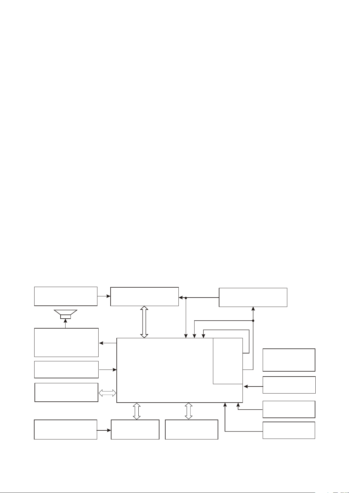
Function introduction
3.1.2 Block diagram of the player
Block diagram of the player is shown in the figure 3.1.2.1:
32.768K
CRASTAL
HEADPHONES
ANTI-POP CIRCUIT
IMPEDANCE MATCH
FM MODULE
LDO MODULE
3.0V VOLTAGE
2.8V
VOLTAGE
1.8V VOLTAGE
MICROPHONE
USB INTERFACE
3V-12V DC-DC
CONVERTER
PNX 0101
OLED MODULE
Figure 3.1.2.1 block diagram
NAND
FLASH MEMORY
- 12 -
ONE AAA SIZE
DC-DC
INTERNAL
CONVERTER
BATTERY
BUTTON ARRAY
RESET CIRCUIT
12M CRYSTAL
Page 17
3.1.3 Introduction to IC of the player
Location IC model Function
U1 PNX0101ET MP3 decode
U2 K9F4G08U0M Flas h
U3 TCM809ZVBN713 Reset IC
U4 TPS793285DBVR Precision voltage stabilizer
U5 SI1912 Dual MOS tube
U6 LM2703 12V boos t
FU1 TEA5767HN TuningIC
Introduction to IC of the player is shown as in the following table:
- 13 -
Page 18
Section Two Unit Circuit Principle
3.2.1 FLASH circuit
1. FLASH circuit schematic diagram is shown in the figure 3.2.1.1:
U2
K9F2G08U0M-YCBO TSOP
NC
NC
NC
NC
NC
GND
RY/BY
RE
CE
NC
NC
Vcc
Vss
NC
NC
CLE
ALE
WE
WP
NC
NC
NC
NC
NC
NC
NC
NC
NC
I/O8
I/O7
I/O6
I/O5
NC
NC
NC
Vcc
Vss
NC
NC
NC
I/O4
I/O3
I/O2
I/O1
NC
NC
NC
NC
48
47
46
45
44
43
42
41
40
39
38
37
36
35
34
33
32
31
30
29
28
27
26
25
MPMC_AD7
MPMC_AD6
MPMC_AD5
MPMC_AD4
MPMC_AD3
MPMC_AD2
MPMC_AD1
MPMC_AD0
VCC33
L13 601
R16 100K
FLASH3V3
C48
104 X5R
D_GND
R17
100K
1
2
3
4
5
6
/CE
/WP
7
8
9
10
11
12
13
14
15
16
17
18
19
20
21
22
23
24
/RE
D_GND D_GND
CLE
ALE
/WE
D_GND
FLASH3V3
C19
104 X5R
D_GND
Figure 3.2.1.1 Flash circuit schematic diagram
2. Working principle: Flash Memory is the storage unit of the player, all Mp3 and waveform files
should be stored in FLASH. Flash module is composed of FLASH chip TC58512FT and peripheral circuit
to finish internal files’s working of read, write and delete. 1.5V battery voltage, through PNX0101 internal
boosted circuit, provides 3.3V voltage for working of FLASH. R16 is pull up resistor of /CE, R17 is the
pull down resistor of /WP, Vcc is power supply pin of FLASH, /CE is chip selection signal, high level is
effective, VCC33 provides 3.3V voltage and FLASH begins to work. /RE, /WE are read effective and
write effective signal end respectively to control read and write function of FLASH. I/O1 - I/O8 are 8 data
lines to complete the exchange of FLASH and external data to realize functions of write, delete and edit
of Mp3.
- 14 -
Page 19
When Mp3 is powered on, 3.3V voltage supplies power for Flash through Vcc, /CE inputs 3.3V high
level signal and Flash begins to work effectively. When Mp3 laying music, /RE is high level, Flash
performs read operation. When writing files in through data line o recording through microphone, /WE is
high level, Flash performs write in operation. Working of read out and write in are performed through
I/O1 I/O8 8 data/address lines.
3.2.2 FM tuning circuit
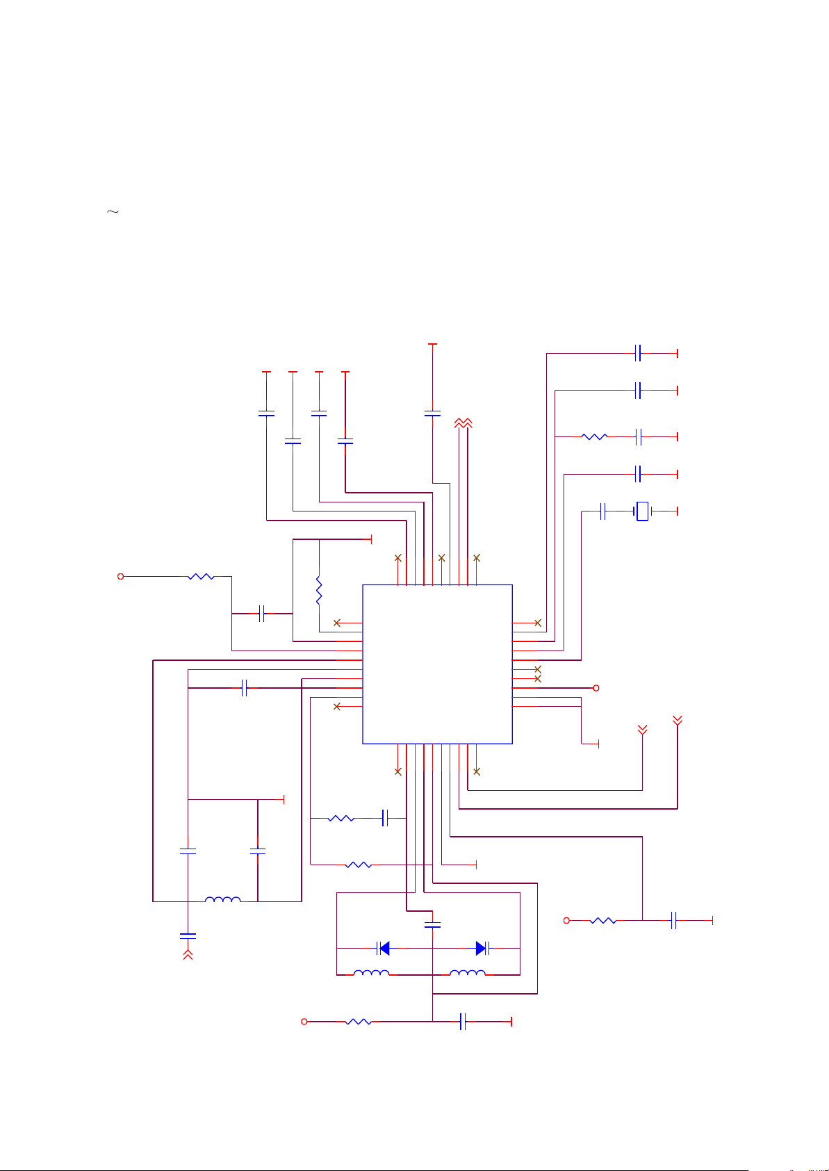
1. FM tuning circuit diagram is shown in the figure 3.2.2.1;
102
C18
29
30
N.C
N.C
IFGAI
AGND
AVCC
RFI1
RFGND
RFI2
TCAGC
LOOPSW
N.C
N.C
CPOP2VCOT13VCOT24VCOVCC5DGND6DVCC7DATA8CLOCK9N.C
1
SGND
FM_OUTL
FM_OUTR
C12 333
FM_OUTL
FM_OUTR
21
22
23
24
26
27
N.C
LAVO
MPXO25VREF
DIFL128DIFL2
RAVO
TCIFC
TMUTE
NECTAR-I
TEA5767HN
N.C
20
PHLF
19
PDLF
18
XTAL2
17
XTAL1
16
SWP2
15
SWP1
14
BUSEN
13
BUSM
12
W/R
11
10
R6
C17
223
C16
33K
C14
223
SGND SGND SGND
C15
22PF
102
D-GND D-GND
XT1
CRYSTAL
32.768KHz
FM_3V3
D-GND
IIC_SDA 2
IIC_SCL 2
SGND
SGND
C6 473
C7 473
R1
10R
FM_3V3
C5
475/X5R/0603
C3
472
SGND
SGND
C8 473
C9 333
SGND
U1
R2 18K1%
31
32
33
34
35
36
37
38
39
40
C10
R3
SGND
C4
C2 27PF
101
FM_ANT
C1
FM_ANT3
47PF
L1
120nH/2%
FM_3V3
10K
R5
33nH2%
393
100K
D-GND
C19
103
C11
L3
33nH2%
C13
BB202
D2
FM_3V3
SGND
dandu
R7
22R
BB202
D1
L2
R4
22R
104/X5R/0402
104/X5R/0402
D-GND
Figure 3.2.2.1 FM tuning circuit diagram
- 15 -
Page 20
2. Working principle: tuning circuit is composed of micro digital tuning IC TEA5767HN of Philips
company and peri
pheral circuit. Power supply voltage is supplied by PQ1X28 to provide pure voltage
with value 2.8V for IC. FC1, FC2, FC3, FC4 and Fl1 are antenna input matched circuit of FM module;
variable diode Fd1, Fd2 and winding inductor is tuning circuit in FM module. Control of FM adopts IIC
bus control means, 8, 9 of TEA5767 are data line and control line.
When MP3 player switches to FM tuning state, pin 13 BUSEN of TEA5767HN receives high level
signal, bus control mode is gated, IC begins to work. As antenna, headphone receives FM signals from
nature, through antenna input matching circuit, input TEA5767HN, PNX0101 via RFI1 and RFI2 to
control TEA5767HN to perform intermediate frequency and selected frequency control through IIC_SCL
and IIC_SDA to transform FM signals to sound simulating signals and then is outputted by FM_OUTR
and FM_OUTL to ADC circuit of PNX0101 and then output through headphone after DAC processing.
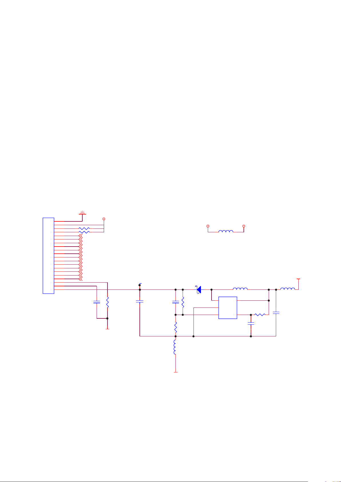
3.2.3 OLED module circuit
1. OLED module circuit is shown in the figure 3.2.3.1:
GND
CN5
1
2
BS2
BS1
IREF
VCOMH
VOLED
R43 4.7K
R44 4.7K
LCD_CS 1
LCD_RESET 1
LCD_D/C 1
LCD_WR 1
LCD_RD 1
LCD_DB0 1
LCD_DB1 1
LCD_DB2 1
LCD_DB3 1
LCD_DB4 1
LCD_DB5 1
LCD_DB6 1
LCD_DB7 1
3
4
5
6
7
8
9
10
11
12
13
14
15
16
17
18
19
20
LCD_3V3
VOLED1
D4
MBR0520/SOD123
L22
601
L25
CR32NP-10uH
LCD_3V3VCC33
VCC33
L14 601
CON20
C55
104/16V
R47
2M
D_GND
C62
106/25V/1206
C65
22P
R53
27K1%
D_GND
L23
0R
R49
240K1%
U6
Lm2703
VIN
EN
5
R1
C18
104
100K
C54
475/X5R/6.3V
4
1
SW
2
GND
3
FB
Figure 3.2.3.1 OLED circuit schematic diagram
2. Working principle: 12V high voltage is required to lighten OLED and matching circuit must be
matched to finish. The circuit includes two parts: boosted circuit and OLED jack circuit, in which boosted
circuit is constituted by boosted DC-DC LM2703 and peripheral circuit, VIN is power input, EN is
Lm2703 enable end, high level is effective, SW is high voltage output pin, FB is feedback pin, voltage
- 16 -
Page 21
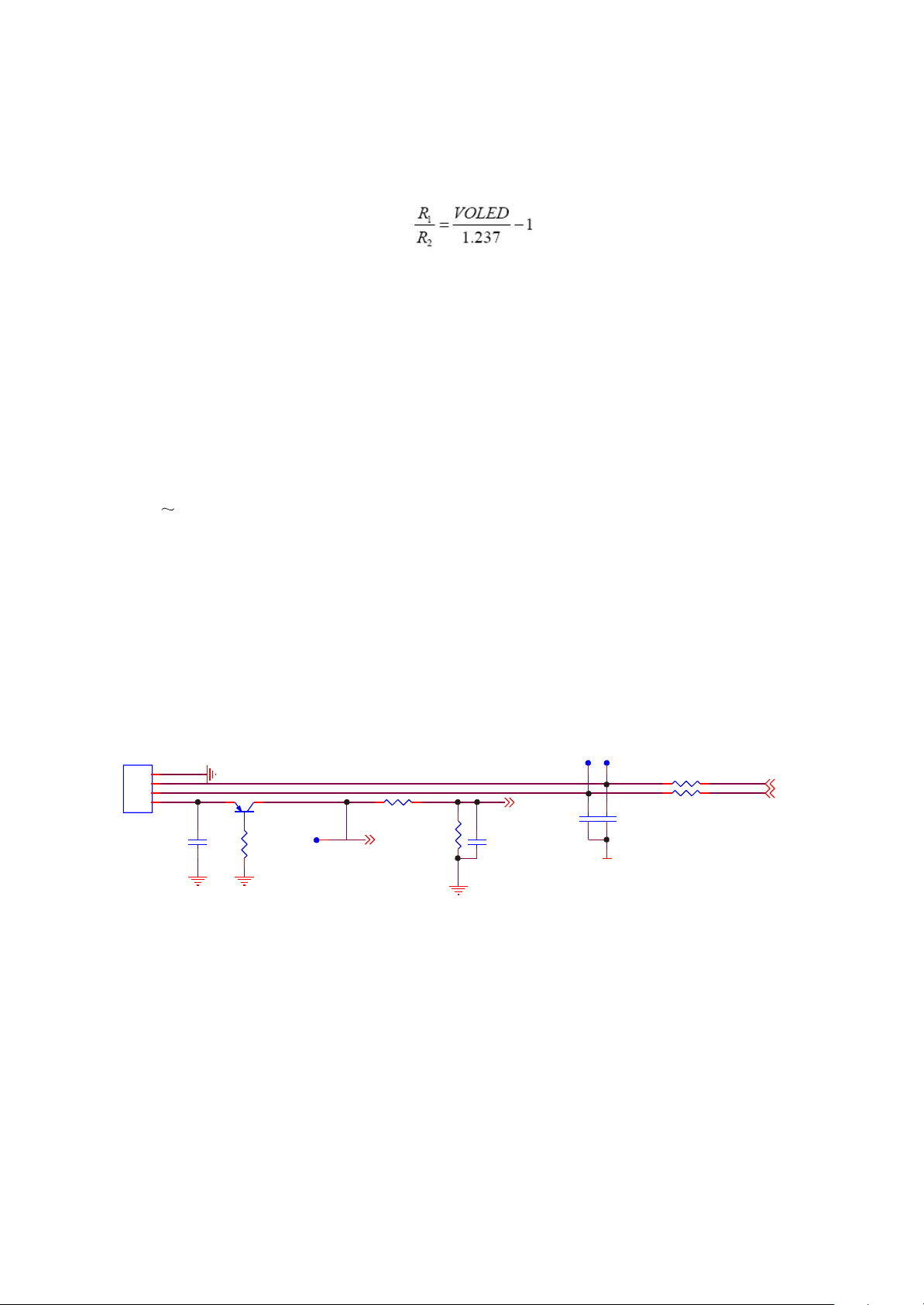
Value VOLED outputted by high voltage is achieved through selecting two voltage partial resistor on two
ends of FB, and the following relation is met:
Seen from the above, VOLED is about 12.2V. L25, C62 in circuit are energy storage inductor and
output capacitor of boosted circuit.
3.3V voltage inputs LM2703 through Vin, EN receives the high level through current limit by R1 to
make LM2703 effective, 3.3V voltage is outputted by SW pin through LM2703 voltage rise, output to pin
20 of OLED through voltage stabilizing pipe D4 to provide lighting voltage for OLED. During the course
of working, FB feedback to LM2703 through detecting energy storage capacitor C65, output voltage
may be controlled through adjusting resistor R49 and R53.
OLED jack circuit is connected with OLED of PNX0101 directly, through data exchange of
LED_DB0 LED_DB7 and PNX0101, character display is controlled by internal program of PNX0101.
Pin 6 of OLED is reset signal and controlled by one MPMC jack of PNX0101. When power on, high
level outputs and OLED resets.
3.2.4 USB jack circuit
1. USB jack circuit is shown in the figure 3.2.4.1:
USB1
4
GND
3
D+
2
D-
1
VB+
SFI0402-050E100NP
C60
GND
GND
Q1 SS8550LT
R3
1K
GND
USB_VBUS
R59 100K
USB-VBUS
1
R77
180K
GND
USB_DET 1
SFI0402-050E100NP
C69
104 X5R
Figure 3.2.4.1 USB jack circuit schematic diagram
2. Working principle: USB jack network is composed of VB+ (USB 5V power), D+ (positive data line),
D- (negative data line) and GND (ground line), in which PNP triode Q1 is used for inverse insert
protection to prevent damaging Mp3 internal circuit because of inverse insert.
D with USB control module of PNX0101 directly. When Mp3 is connected with computer, VB+ high
DM DP
C8
C9
SFI0402-050E100NP
D_GND
R5 18R
R7 18R
USB_DP 1
USB_DM1
level of computer USB jack inputs to USB_DET of PNX0101, USB jack is effective, USB jack connects
with PNX0101 through D+ (USB_DP) and D- (USB_DM), then connected with Flash by PNX to realize
information exchange of Flash internal data and computer internal data.
- 17 -
Page 22
3.2.5 Buttons circuit
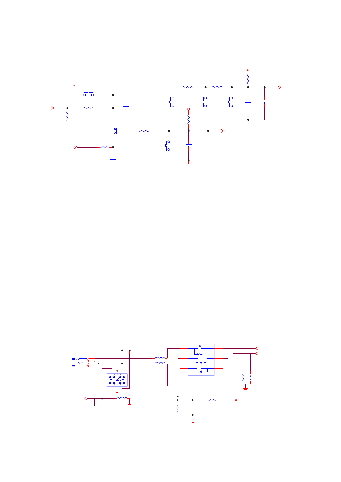
1. Buttons circuit is shown in the figure 3.2.5.1:
VCC33
S1
VOL-
MENU
VOL-
D_GND
DFU
R9
47K
R6 1K
SS8550LT
R4 0R
C14
SFI0402-050E100NP
D_GND
Q5
C11
104 X5R
D_GND
R8 51K
Figure 3.2.5.1 Buttons circuit schematic diagram
S3
D_GND
D_GND
S2
PREV
R15 1k
VCC33
D_GND
R10
1K
C12
104 X5R
R14 1K
S4
NEXT
D_GND
C13
SFI0402-050E100NP
S5
VOL+
D_GND
KEY_SCAN_1 2
VCC33
C66
104 X5R
D_GND
R13
1K
C15
SFI0402-050E100NP
KEY_SCAN_2 2
2. Working principle: buttons of X23 (RU) are composed of 6 single buttons (one is OPEN/CLOSE
and PLAY button, which will be introduced in power on/off circuit). Button detect is to use partial voltage
mode to utilize ADC circuit of PNX0101 to check preset button voltage value to decide which button
functions. When the relevant button is pressed, voltage value of preset point corresponding to this
button will have change, voltage inputs ADC circuit of PNX0101, then the internal program makes the
relevant response to realize function of each button. To lock button.
3.2.6 Headphone jack circuit
1. Headphone jack circuit is shown in the figure 3.2.6.1:
R79
47K
U5
1
S1
2
G1
3
D2
Si1912DL SOT-363/NT4401
R78
C1
104 X5R
6
D1
5
G2
4
S2
4.7K
R501KR51
PHONE_MUTE 1
HP_VOUTL 1
HP_VOUTR 1
1K
1
3
4
2SJ-A382-001(HP-DC)
5
CN1
FM_ANT
FM_ANT
OUT_R
4
5
162
3
GND
601 DCR<350m
L17
OUT_L
601 DCR<350m
L15
601 DCR<350m
L16
D1
RCLAMP0504F/SC-706L
GND
Figure 3.2.6.1 Headphone jack circuit schematic diagram
- 18 -
Page 23

2. Working principle: left and right channels audio signals outputted from PNX0101 , through 220uF
capacitor coupling output, are sent to headphone jack circuit. Headphone jack circuit is composed of the
dual MOS tube SI1912DL and headphone socket CN1 that control sound output. Pin 2 and 5 of
SI1912DL are connected to mute circuit. When MUTE button is pressed, control dual MOS tube is
disconnected to cut the output of left and right channels of headphone. D1 in circuit is TVS diode array,
used to protect ESD to prevent external static from damaging internal circuit through headphone jack.
Ground wire of headphone is also used as antenna input of FM tuning.
3.2.7 Power on/off control circuit
1. Power on/off control circuit of X17 (RU) is shown in the figure 3.2.7.1:
START1
SFI0402-050E100NP
C72
START
VCC33
BAT+
1
3
D3
MMBD4148CC
2
R11
1K
PLAY/PAUSE
L24
10UH
SW
START/PLA Y/PAUSE
D_GND
Figure 3.2.7.1 Power on control circuit schematic diagram
2. Working principle: power on/off is completed through operating ON/OFF button S1. When
pressing S1 to power on, S1 is connected, high voltage of STAET point is pulled down to ground, START
sends out low level signal, L17 of PNX0101 is connected to START signal DC-DC to begin to work and
provide 3.3V and 1.8V voltage, D17 pin of PNX0101 is connected to START signal at the same time and
system power on.
Power off of X23 (RU) is realized through software. During the course of working, press S1 for a
long time, PNC0101 detects START signal through D17, low level sends out this power-off signal to
make the player stop working; if low level is short time, it is PLAY or PAUSE.
- 19 -
Page 24

3.2.8 Reset circuit
1. Reset circuit is to provide power0on reset level for PNX0101. Reset circuit is shown in the figure
3.2.8.1:
U3
VCC33
TCM809Z
2
VCC
RESET
GND
1
3
P_GND
R2
0R
RESET
SFI0402-050E100NP
C78
D_GND
Figure 3.2.8.1 Reset circuit schematic diagram
2. Working principle: reset circuit is composed of reset IC G690L263 (U2) and peripheral circuit. At
the moment of power of the player, level of pin 2 of G690L263 changes from 0V to 3.3V pin 1 outputs a
low level reset pulse signal with pulse width 140 millisecond and inputs to pin T14 of PNX0101 to reset
the player. After reset finishes, high level is maintained, C11 in circuit is voltage dependent resistor and
used for anti-static.
3.2.9 MIC circuit
1. MIC circuit is shown in the figure 3.2.9.1:
DAC_VDDA33
Q4
MMST3904
R62
100K
R45
470K
MICROPHONE
MIC1
C58
106 X5R
Figure 3.2.9.1 MIC circuit schematic diagram
GND
- 20 -
R67
2.2K
C61
104 X5R
ADC_MIC
ADC_MIC 1
Page 25

2. Working principle: MIC circuit is composed of microphone and microphone power bias circuit.
MIC1 switches the external voice signals recorded to electric signals, through C61 coupling, and outputs
ADC circuit of PNX0101 to switch analog electric signals to digital signals to form WAV file through
software encoding to save in FLASH. R62, R45, Q4 and C56 in circuit is triode voltage stabilizing
system, which provides stable power bias for microphone, R67 is bias resistor of microphone.
3.2.10 Low voltage detecting circuit
X23(RU) has no special low voltage detecting circuit. Battery voltage detecting is controlled through
PNX0101 internal software, M17 pin of PNX0101 is connected to anode of battery, internal program sets
the lowest voltage of power off, when M17 pin of PNX0101 detects that battery anode voltage is lower
than this value, power off signal sends out to realize system power off.
- 21 -
Page 26

Section Three Servicing Cases
3.3.1 Servicing cases
[ Example 1 ] Symptom: power not on
Description: no OSD, no output
Analysis and troubleshooting: firstly analyse whether it is caused by battery or by power circuit. If
power not on, firstly connect with computer and check whether screen has display. Power on, connect
and there is no display, so take machine apart and check it. Firstly check power battery voltage and it
Cannot be lower than 1.3V, then check VCC 3.3V and 1.8V outputted through BGA and find that 3.3V is
low, which is normal and 1.8V is normal; after pressing ON button and the player is working normally,
VCC 1.8V should be pulled down to about 1.4V, VCC3.3V should be lower to 3.1~3.2V when working
normally; then test crystal oscillator, oscillation is normal, frequency is 24MHZ and reset is also normal,
so we analyse that it is chip that is not working; working conditions are normal, so we analyse that it os
drive program that has problem; upgrade DFU again and trouble is removed.
[ Example 2 ] Symptom: not connect with computer
Description: connect with computer, no response and no OSD.
Analysis and troubleshooting: firstly confirm whether power-on is available and the result is normal;
then check USB circuit, check whether 4 pin flat cable from USB socket to mai board has open circuit
(please note 4 Pin welding position of this model player is easy to break, so you cannot test flat cable
directly and you must test from ,USB socket Pin to USB terminal Pin). Use diode level of multimeter to
ground, test the resistance to ground of D+, D- data signals in USB terminal position and it should be
close to several hundred ohm; then test between D+ and D- and short circuit is not allowed (test 2 pins
in the middle of USB terminal); test and find that D+ resistance value is normal, D- resistance value is
infinite, R5 is false welding; after welding again, trouble is removed.
[ Example 3 ] Symptom: noise appears when tuning
Description: noise appears when tuning.
Analysis and troubleshooting: firstly judge whether tuning components or common part has trouble,
whether one side of headphone has sound when listening, and the result is normal; then switch to tuning
- 22 -
Page 27

State, search radio station automatically, tuning is normal, which means power supply, data and clock
are normal; we remote external interference, receive the nearest local radio station and check whether it
is clear, and the result shows noise still exists; circuit that causes noise is high frequency tuning and
mixed frequency part; carefully check and find that pin 37 of tuning IC is false welding; weld again and
trouble is removed.
[ Example 4 ] Symptom: noise appear when playing
Description: headphone output noise when playing
Analysis and troubleshooting: if there is noise when playing, it is BGA that has trouble, for playback
and other functions are all normal, only there is noise, so it is necessary to analyse whether decode [art
or rear stage causes this trouble, when playing 1KHZ standard signal, there should be sine wave signals
and not any noise; test C31, C32 waveform close to BGA, so we judge that it is BGA that has trouble;
after changing it, trouble is removed.
[ Example 5 ]Symptom: player not switched on
Description: after pressing ON button, screen has no display and headphone has no output.
Analysis and troubleshooting: firstly conform whether the trouble is player not switched on or power
supply not connected; connect with computer and check whether display of screen is normal; connect to
adapter, if display of charge can be displayed, it means that power and rear stage circuit work normally;
power on/off circuit is shown in the figure 3.3.1.1, power on/off circuit, through a light touch switch S1,
shuts and then forms loop to generate a Start signal to enter chip detect and then power on; firstly test
S2 switch, press CLOSE and check whether it is on and find that S2 is false welding when testing; after
welding again, trouble is removed.
VCC33
START
START
BAT+
1
3
D3
MMBD4148CC
2
R11
1K
PLAY/PAUSE
L24
10UH
SOT23
SFI0402-050E100NP
C72
S1
START/PLA Y/PAUSE
D_GND
Figure 3.3.1.1 ON/OFF circuit schematic diagram
- 23 -
Page 28

[ Example 6 ] Symptom: screen has mosaic
Description: display screen has mosaic and display has disorder
Analysis and troubleshooting: this troubleshooting is the same with that of no screen display, with
the difference is that power supply is normal; firstly confirm whether the screen itself has trouble or
circuit has trouble, change display screen and trouble still exists, then use oscillograph to test the 8-digit
number of OLED screen and find that flat cable holder of display screen has false welding, after welding
again, trouble is removed.
[ Example 7 ] Symptom: noise when recording
Description: there is noise when playing record files
Analysis and troubleshooting: schematic diagram of record circuit is shown in the figure, it is mainly
composed of microphone and microphone power bias circuit, MIC circuit schematic diagram is shown in
the figure 3.3.1.2. MIC switches the external voice signals recorded into electric signals, through being
coupled by C61, output to ADC circuit of PNX0101 and form WMA files through software coding to save
in Flash.
When repairing this kind of machine, firstly play files and check whether there is noise and there is
no; check recording circuit and power supply is normal; when recording, use oscillograph to test C61
and there is noise interference, after changing MIC, trouble is removed.
DAC_VDDA33
Figure 3.3.1.2 MIC circuit schematic diagram
Q4
MMST3904
R62
100K
R45
470K
MICROPHONE
C58
MIC1
106
GND
R67
2.2K
C61
104
ADC_MIC
ADC_MIC 1
[ Example 8 ] Symptom: no OSD
Description: screen has no display
Analysis and troubleshooting: firstly confirm whether trouble lies in power or screen itself; power on
and listen to the sound and sound s normal, so it is preliminarily judged that power supply 3.3V and 1.8V
are both basically normal. Firstly test voltage on two ends of L25 and it is about 4.3V, which is Basically
- 24 -
Page 29

Normal; then test voltage on two ends of D4 and find that anode has no 12.5V voltage, take down
display screen and there is still no; check input end voltage and enable voltage and they are basically
normal, then check FB end voltage of feedback pin and it is obviously low, check and find that IC U6 has
trouble, after changing it, trouble is removed.
[ Example 9 ] Symptom: only one side has sound output
Description: only one side of headphone has output when playing.
Analysis and troubleshooting: because only one side has normal sound output, it means that other
circuits are normal, secondary output DAC circuit is shown in the figure 3.3.1.3, firstly check whether
headphone terminal has false welding, test waveform on two ends of headphone terminal and find that
left channel has no waveform, then test capacitor C32 and there is still no wave, then test C28 and
reference level is obviously low comparing with right channel, test resistor to ground and it is only
dozens of ohm, take down BGA and test and find that resistance to ground is infinite, after changing
BGA, trouble is removed.
M3
DAC-VOUTR
M2
DAC-VOUTL
P3
HP-OUTR
N3
HP-OUTL
N2
HP-OUTCA
N1
HP-OUTCB
DAC
HP_VOUTR
HP_VOUTL
C31 220UF/4V
C32 220UF/4V
C40 104
C34 104
Figure 3.3.1.3 DAC circuit diagram
C27 332
C28 332
R29 10R
R30 10R
[ Example 10 ] Symptom: no sound when playing
Description: headphone has no output when playing
Analysis and troubleshooting: firstly adjust volume to maximum and play1KHZ standard signals,
2.8V power switch circuit is shown in the figure 3.3.1.4, check whether two ends of output end C31, C32
have waveform and there is no, then test resistance to ground of reference level end C27, C28 and it is
normal, then test audio power supply IC U4 and pin 1 of input end is 3.3V, which is normal, when testing
Pin 5 of output end and voltage is 0.6V, which should be 2.8V when in normal conditions, so it is on low
side obviously, after changing IC, trouble is removed.
VCC33
LD298 2/LP2985/S1167/PQ1X281M2ZP/TPS793285SOT23
C36
106/X5R
P_GND
Figure 3.3.1.4 2.8V power switch circuit schematic diagram
1
VI
2
GND
EN3BYPASS
U7
VOUT
- 25 -
5
4
104
D_GND D_GND
-5
C46
106/X5RC42
Page 30

3.3.2 Troubleshooting flow chart
1.Troubleshooting process for “No screen display”.
No screen display
Check
whether D8 anode
12V voltage is
normal
Y
Check
whether 12V
voltage is on display
screen socket
Y
Change
display screen
components and check
whether they are
ok
Y
Display screen has trouble
N
Check DC-DC boosted
circuit and surrounding
elements
N
Flat cable holder of display
screen is false welding
N
Flat cable holder of display
screen has trouble
Figure 3.3.2.1 Trouble shooting flow chart for “No screen display”
- 26 -
Page 31

2.Troubleshooting process for USB not connected”.
USB not connected
Q1 outputs
4.8V and whether
it is normal
Y
Check
whether 3.3V, 1.8V
are normal
Y
Check
whether 12M
crystal oscillator’s
oscillation is
normal
Y
Check
resistance to
ground of D+, D- (red
means grounding,
use diode level to
test )
Y
Change BGA
N
Q1 has trouble or USB
socket has false welding
N
Check each DC-DC switch
circuit and peripheral elements
N
Change crystal oscillator
or capacitors on two sides
N
Check T1 or change BGA
Figure 3.3.2.2 Troubleshooting plow chart for “USB not connected”
- 27 -
Page 32

3.Troubleshooting process for “Buttons have no function”.
Buttons have no function
Confirm
whether all buttons
have no
function
Y
whether machine
failure
N
Whether
3.3V circuit output is
normal
Y
Check R8, R10
N
Change a certain button
Y
N
Change BGA
Change BGA
Figure 3.3.2.3 Troubleshooting flow chart for “Buttons have no function”
- 28 -
Page 33

4 Troubleshooting process for “No tuning function”
No tuning function
Whether
it ca switch to tuning
mode
Y
Whether
it can switch to auto
search
Y
Whether
there is click sound
Y
Check antenna high
frequency input loop
N
Check power supply
oscillation, data I C circuit
N
Check SCL, SDA signal
N
Check
whether BGA has tuning
signal
BGA has trouble
2
Y
Figure 3.3.2.4 Troubleshooting flow chart for “No tuning function”
- 29 -
Page 34

5.Troubleshooting process for "Power not on"
Power not on
whether 3.3V,
1.8V output is
N
software upgrading
again is normal
Program lost
Check
normal
Y
Whether
Y
N
whether BGA working
condition, power supply, clock
Connect
to computer and check
whether there is
screen
display
Y
Whether
battery voltage is lower
than 1.3V
Y
Change battery
Check
and reset circuit
are normal
Y
Change BGA
N
Change BGA
N
Check L18, L28, R24
and circuit around
N
Check each branch circuit
Figure 3.3.2.5 Troubleshooting flow chart for “Power not on”
- 30 -
Page 35

Section Four Waveform diagram
This section collects signal waveform diagram of audio, video and each unit circuit with the purpose
to help servicing personnel to judge where trouble lies in accurately and quickly to improve servicing
skills. For the difference of oscillograph's type, model and tuner, a certain difference may exist, so the
servicing personnel are expected to pay more attention to check in daily operation.
1. 12M crystal oscillator oscillation waveform diagram
2. L25 boosted energy storage waveform diagram
- 31 -
Page 36

3. LCD_3V3 waveform diagram
4. Software power supply 3V3 waveform diagram
5. LCD_RESET waveform diagram
- 32 -
Page 37

6. LCD_CS waveform diagram
7. LCD_WR waveform diagram
8. LCD_D/C waveform diagram
- 33 -
Page 38

9. LCD_DB0 waveform diagram
10. LCD_RD waveform diagram
11. LCD_DB2 waveform diagram
- 34 -
Page 39

12. LCD_DB1 waveform diagram
13. LCD_DB4 waveform diagram
14. LCD_DB3 waveform diagram
- 35 -
Page 40

15. LCD_DB6 waveform diagram
16. LCD_DB5 waveform diagram
17. IREF waveform diagram
- 36 -
Page 41

18. LCD_DB7 waveform diagram
19. VOLED waveform diagram
20. VCOMH waveform diagram
- 37 -
Page 42

Section Five Function Introduction to IC
3.5.1 Function introduction to PNX0101ET
1. Description
The PNX0101 (ARM-based Solid State Audio IC) is an IC based on an embedded RISC processor. The
device is designed for hand -held Solid State Audio applicat ions like portable MP3 players. The high level of
integration, low power consumption and high processor performances make the PNX0101 very suitable for
portable hand-held devices.
The PNX0101 is based on the powerful ARM7TDMI CPU core, which is a full 32 -bit RISC processor with
8 kbyte dedicated cache.
2. Features
2.1 General Features
◆ One chip solution for compressed audio players using flash memory
◆ Programmable architecture enables flexible support of “up-coming” digital music formats
– This hold for running the decoder on the ARM
– The decoders on the low-power DSP, are running from mask ROM
◆ FM Radio input and control support
Embedded program flash for easy upgradi ng and increased program security◆
Support for Philips LifeVibes◆
Small footprint package TBGA180 10x10mm 0.5pitch◆
2.2 Hardware Features
ARM7TDMI + 8kByte cache◆
Embedded 64kByte RAM and 32 kByte ROM◆
Integrated embedded program Flas h (4M bit)◆
Ultra low power Audio DSP for support of Philips LifeVibe◆ sTM audio enhancement algorithms (storede
in teh DSP’s
TM
audio enhancement algorithms
ROM).
External memory support: Nand Flash/Compact flash/MMC/SMC/SRAM/ROM/SDRAM◆
Integrated MCI interface◆
Integrated USB 2.0 FS compliant slave interface (for firmware upgrade, data support from/to◆ PC,
streaming audio)
- 38 -
Page 43

Intelligent Configuration Power Management◆
Single battery operat ed embedded DC/DC converter◆
Integrated 6800/8080 compatible LCD i nterface◆
General◆ -Purpose IO pins (nearly all pins can be configured as GPIO pins)
Integrated Ma◆ ster/Slave IIC interface
Integrated ADC with line input and voice input (with recording possibility)◆
Built◆ -in ADC for level measurement & control (5 -inputs)
Integrated DAC with line output, headphone output with short◆ -circuit protection
Integrated ◆ IIS input and output interface
Integrated SPDIF receiver◆
Integrated UART + IRDA◆
Integrated Real Time Clock with alarm◆
Boundary scan◆
2.3 Possible software features
MP3 encoding/decoding (*) => Support for MPEG 1 layer 3 and MPEG 2 layer 2.5 and la◆ yer 3 audio
decoding (MP3)
WMA decoding (*)◆
AAC decoding (*)◆
Ogg Vorbis decoding (*)◆
Voice recording using A DPCM◆
Intelligent power management software◆
USB Mass Storage Class◆
USB Device Firmware Upgrade◆
Philips LifeVibesTM sound enhancement ◆ software including bass/treble/volume control.
(*) Audio decoders/encoders do need appropriate licenses.
3. PIN Description
SYMBOL
BGA
BALL
12 MHz oscillator (fixed: 4 pins)
XTALH_IN T10 A input apio (ZI) 12 MHz clock input
DIGITAL
APPL.
I/O
FUNC
LEVEL
PIN STATE
AFTER
RESET
CELL
DESCRIPTION
TYPE
XTALH_OUT V9 A output apio (IO) 12 MHz clock output
XTALH_VDDA18 U9 vddco Analog supply Oscillator
XTALH_VSSA T9 vssco Analog ground Oscillators
32.768 kHz oscillator (fixed: 4 pins)
- 39 -
Page 44

XTALL_IN V7 A input apio (ZI) 32.768 kHz clock input
XTALL_OUT T8 A output apio (ZI) 32.768 kHz clock output
XTALL_VDDA18 U8 vddco Analog supply Oscillators/PLL’s
XTALL_GNDA V8 vssco Analog ground Oscillators/PLL’s
bitslicer/SPDIF (fixed: 3pins)
SPDIF_IN T12 A input apio (IO) SPDIF input
SPDIF_VDDA33 U11 vddco Analog supply SPDIF input
SPDIF_GNDA T11 vssco Analog ground SPDIF input
10-bit ADC (fixed: 7 pins)
ADC10B_GPA4 U5 A input apio (ZI) Analog General Purpose pins
ADC10B_GPA3 T6 A input apio (ZI) Analog General Purpose pins
ADC10B_GPA2 U6 A input apio (ZI) Analog General Purpose pins
ADC10B_GPA1 T7 A input apio (ZI) Analog General Purpose pins
ADC10B_GPA0 U7 A input apio (ZI) Analog General Purpose pins
ADC10B_VDDA33 V10 vddco Analog supply 10-bit ADC
ADC10B_GNDA U10 vssco Analog ground 10-bit ADC
DAC (fixed: 13 pins)
DAC_VOUTR M3 A output apio (IO) SDAC Right Analog Output
DAC_VOUTL M2 A output apio (IO) SDAC Left Analog Output
DAC_VDDA33 L1 vddco SDAC Positive Voltage
DAC_VREFP L2 A input apio (IO) SDAC Positive Reference Voltage
DAC_VREFN M1 A input apio (IO) SDAC Negative Reference Voltage
HP_OUTR P3 A output apio (IO) SDAC Right Headphone Output
HP_OUTL N3 A output apio (IO) SDAC Left Headphone Output
HP_OUTCA N2 A output apio (IO) Headphone common output reference
HP_OUTCB N1 A output apio (IO) Headphone common output reference
HP_VDDA33A R1 vddco Headphone analog supply
HP_VDDA33B R2 vddco Headphone analog supply
HP_GNDAA P2 vssco Headphone analog ground
HP_GNDAB P1 vssco Headphone analog ground
ADC (fixed: 11 pins)
ADC_VCOM T3 A input apio (IO) ADC Common Reference Voltage
ADC_VREFP U2 A input apio (IO) ADC Positive Reference Voltage
- 40 -
Page 45

ADC_VREFN V1 A input apio (IO) ADC Negative Reference Voltage
ADC_VDDA18 V3 vddco Analog supply ADC
ADC_VDDA33 U3 vddco Analog supply ADC
ADC_GNDA V2 vssco Analog ground ADC
ADC_VREF U1 A input apio (IO) ADC Reference Voltage
ADC_VINR T1 A input apio (IO) SADC Right Analog Input
ADC_VINL T4 A input apio (IO) SADC Left Analog Input
ADC_MIC R3 A input apio (IO) Microphone input
ADC_MIC_LNA output Output of LNA of Microphone input
HP_VCOM
T2 A
input
apio (IO)
HP Common Reference Voltage
LCD Interface (fixed: 12 pins)
6800 read/write select 8080 active ‘high’
LCD_RW_WR
GPIO_LCD_11
G2
0-5 VDC
tolerant
I/O
output
bpts10tht
write enable
5v
General Purpose IO pin
6800 enable 8080 active ‘high’ read
LCD_E_RD
GPIO_LCD_10
F2
0-5 VDC
tolerant
I/O
output
bpts10tht
enable
5v
General Purpose IO pin
Data input 7/Data output 7/Serial data
LCD_DB_7
GPIO_LCD_9
E3
0-5 VDC
tolerant
I/O
output
bpts10tht
output/4-bit data 3
5v
General Purpos IO pin
Data input 6/Data output 6/Serial data
LCD_DB_6
GPIO_LCD_8
E2
0-5 VDC
tolerant
I/O
output
bpts10tht
input/4-bit data 2
5v
General Purpose IO pin
LCD_DB_5
GPIO_LCD_7
LCD_DB_4 Data input 4/Data output 4/4-bit data 0
GPIO_LCD_6
LCD_DB_3 Data input 3/Data output 3
GPIO_LCD_5
LCD_DB_2 Data input 2/Data output 2
GPIO_LCD_4
LCD_DB_1 Data input 1/Data output 1
GPIO_LCD_3
D3
D1
D2
C3
C1
0-5 VDC
tolerant
0-5 VDC
tolerant
0-5 VDC
tolerant
0-5 VDC
tolerant
0-5 VDC
tolerant
I/O
I/O
I/O
I/O
I/O
output
output
output
output
output
- 41 -
bpts10tht
5v
bpts10tht
5v
bpts10tht
5v
bpts10tht
5v
bpts10tht
5v
output/4-bit data 1
General Purpos IO pin
General Purpose IO pin
General Purpose IO pin
General Purpose IO pin
General Purpose IO pin
Data input 5/Data output 5/Serial clock
Page 46

LCD_DB_0 Data input 0/Data output 0
GPIO_LCD_2
C2
0-5 VDC
tolerant
I/O
output
bpts10tht
5v
General Purpose IO pin
LCD_CSB Chip Select
GPIO_LCD_1
B3
0-5 VDC
tolerant
I/O
output
bpts10tht
5v
General Purpose IO pin
‘high’ Data register select ‘low’ instruction
LCD_RS
GPIO_LCD_0
F3
0-5 VDC
tolerant
I/O
output
bpts10tht
register select
5v
General Purpose IO pin
Memory Card Interface (fixed: 6 pins)
MCI_DAT_3 Data input/Data output
GPIO_MCI_5
MCI_DAT_2 Data input/Data output
GPIO_MCI_4
MCI_DAT_1 Data input/Data output
GPIO_MCI_3
MCI_DAT_0 Data input/Data output
GPIO_MCI_2
MCI_CLK MCI clock output
GPIO_MCI_1
J3
J1
J2
H3
G3
0-5 VDC
tolerant
0-5 VDC
tolerant
0-5 VDC
tolerant
0-5 VDC
tolerant
0-5 VDC
tolerant
I/O
I/O
I/O
I/O
I/O
input
input
input
input
output
bpts10tht
5v
bpts10tht
5v
bpts10tht
5v
bpts10tht
5v
bpts10tht
5v
General Purpose IO pin
General Purpose IO pin
General Purpose IO pin
General Purpose IO pin
General Purpose IO pin
MCI_CMD Command input/Command output
GPIO_MCI_0
H2
0-5 VDC
tolerant
I/O
input
bpts10tht
5v
General Purpose IO pin
USB Interface (fixed: 4 pins + (8 pins reserved for future use))
USB_CONNECT_N Soft connect output USB 2.0 FS
GPIO_USB_1
USB_RPU
T15
0-5 VDC
tolerant
I/O
output
bpts10tht
5v
General Purpose IO pin
A apio (IO) Reserved for USB 2.0 HS
USB_DP usb11 Positive USB data line USB 2.0 FS
U17 A input
USB_DP
apio Positive USB data line USB 2.0 HS
USB_DM usb11 Negative USB data line USB 2.0 FS
T17 A input
USB_DM
apio Negative USB data line USB 2.0 HS
USB Supply detection line USB 2.0 FS &
USB_VBUS
U14
GPIO_USB_0
0-5 VDC
tolerant
I/O
input
bpts10tht
USB 2.0 HS
5v
General Purpose IO pin
bpts10tht
USB_RREF P16 I/O
5v
- 42 -
Page 47

USB_GNDA R17 vssco Reserved for USB 2.0 HS
USB_VSSA_REF R16 vccso Reserved for USB 2.0 HS
USB_VSSA_TERM T16 vssco Reserved for USB 2.0 HS
USB_VDDA1 8_PLL U15 vddco Reserved for USB 2.0 HS
USB_VDDA18_BG U16 vddco Reserved for USB 2.0 HS
USB_VDDA33 U18 vddco Reserved for USB 2.0 HS
USB_VDDA33_DRV V18 vddco Reserved for USB 2.0 HS
DAI Interface (fixed: 3 pins)
DAI_BCK DAI Bitclock
H17
GPIO_DAI_2
DAI_WS DAI Wordselect
G17
GPIO_DAI_1
DAI_DATA DAI Serial data input
G16
GPIO_DAI_0
0-5 VDC
tolerant
0-5 VDC
tolerant
0-5 VDC
tolerant
I/O
I/O
I/O
input
input
input
bpts10tht
5v
bpts10tht
5v
bpts10tht
5v
General Purpose IO pin
General Purpose IO pin
General Purpose IO pin
DAO Interface (fixed: 4 pins)
DAO_CLK F16
I/O
output
tolerant
0-5 VDC
DAO_BCK DAO Bitclock
G18
GPIO_DAO_2
0-5 VDC
tolerant
I/O
output
0-5 VDC
DAO_WS F18
I/O
output
tolerant
DAO_DATA DAO Serial data output
GPIO_DAO_0
F17
0-5 VDC
tolerant
I/O
output
bpts10tht
5v
bpts10tht
5v
bpts10tht
5v
bpts10tht
5v
256 fs clock output
General Purpose IO pin
DAO Wordselect
General Purpose IO pin
JTAG (fixed: 6 pins)
0-5 VDC
JTAG_TRST_N T13
I input ipthdt5v JTAG Reset Input (pull-down)
tolerant
0-5 VDC
JTAG_TCK V4
I input ipthut5v JTAG Clock Input (pull-up)
tolerant
JTAG_TMS U12
0-5 VDC
I input ipthut5v
tolerant
JTAG Mode Select Input (external
pull-up)
0-5 VDC
JTAG_TDI T5
I input ipthut5v JTAG Data Input (pull-up)
tolerant
JTAG_TDO U13
I/O
output
tolerant
- 43 -
0-5 VDC
bpts10tht
JTAG Data output
5v
Page 48

JTAG_SEL_ARM U4
0-5 VDC
tolerant
IIC master/slave Interface (fixed: 2 pins)
I input ipthdt5v JTAG selection (pull-down)
IIC_SCL H16
IIC_SDA J17
0-5 VDC
tolerant
0-5 VDC
tolerant
I/O
I/O
input
input
iic400kt5
Serial clock IIC Slave
v
iic400kt5
Serial data IIC Slave
v
MPMC (fixed: 52 pins)
MPMC_D_15 MPMC data input/output 15
B8 I/O
GPIO_MPMC_50
input bpts10th
General Purpose IO pin
MPMC_D_14 MPMC data input/output 14
C8 I/O
GPIO_MPMC_49
input bpts10th
General Purpose IO pin
MPMC_D_13 MPMC data input/output 13
B7 I/O
GPIO_MPMC_48
input bpts10th
General Purpose IO pin
MPMC_D_12 MPMC data input/output 12
C7 I/O
GPIO_MPMC_47
input bpts10th
General Purpose IO pin
MPMC_D_11 MPMC data input/output 11
B6 I/O
GPIO_MPMC_46
input bpts10th
General Purpose IO pin
MPMC_D_10 MPMC data input/output 10
C6 I/O
GPIO_MPMC_45
input bpts10th
General Purpose IO pin
MPMC_D_9 MPMC data input/output 9
C5 I/O
GPIO_MPMC_44
input bpts10th
General Purpose IO pin
MPMC_D_8 MPMC data input/output 8
C4 I/O
GPIO_MPMC_43
input bpts10th
General Purpose IO pin
MPMC_D_7 MPMC data input/output 7
B5 I/O
GPIO_MPMC_42
input bpts10th
General Purpose IO pin
MPMC_D_6 MPMC data input/output 6
A5 I/O
GPIO_MPMC_41
input bpts10th
General Purpose IO pin
MPMC_D_5 MPMC data input/output 5
B4 I/O
GPIO_MPMC_40
input bpts10th
General Purpose IO pin
MPMC_D_4 MPMC data input/output 4
A4 I/O
GPIO_MPMC_39
input bpts10th
General Purpose IO pin
MPMC_D_3 MPMC data input/output 3
A3 I/O
GPIO_MPMC_38
input bpts10th
General Purpose IO pin
- 44 -
Page 49

MPMC_D_2 MPMC data input/output 2
B2 I/O
GPIO_MPMC_37
input bpts10th
General Purpose IO pin
MPMC_D_1 MPMC data input/output 1
A2 I/O
GPIO_MPMC_36
input bpts10th
General Purpose IO pin
MPMC_D_0 MPMC data input/output 0
A1 I/O
GPIO_MPMC_35
input bpts10th
General Purpose IO pin
MPMC_A_20 MPMC address 20
C13 I/O
GPIO_MPMC_34
output bpts10th
General Purpose IO pin
MPMC_A_19 MPMC address 19
B13 I/O
GPIO_MPMC_33
output bpts10th
General Purpose IO pin
MPMC_A_18 MPMC address 18
A13 I/O
GPIO_MPMC_32
output bpts10th
General Purpose IO pin
MPMC_A_17 MPMC address 17
C14 I/O
GPIO_MPMC_31
output bpts10th
General Purpose IO pin
MPMC_A_16 MPMC address 16
B14 I/O
GPIO_MPMC_30
output bpts10th
General Purpose IO pin
MPMC_A_15 MPMC address 15
A14 I/O
GPIO_MPMC_29
output bpts10th
General Purpose IO pin
MPMC_A_14 MPMC address 14
C15 I/O
GPIO_MPMC_28
output bpts10th
General Purpose IO pin
MPMC_A_13 MPMC address 13
B15 I/O
GPIO_MPMC_27
output bpts10th
General Purpose IO pin
MPMC_A_12 MPMC address 12
C16 I/O
GPIO_MPMC_26
output bpts10th
General Purpose IO pin
MPMC_A_11 MPMC address 11
B16 I/O
GPIO_MPMC_25
output bpts10th
General Purpose IO pin
MPMC_A_10 MPMC address 10
C17 I/O
GPIO_MPMC_24
output bpts10th
General Purpose IO pin
MPMC_A_9 MPMC address 9
B17 I/O
GPIO_MPMC_23
output bpts10th
General Purpose IO pin
MPMC_A_8 MPMC address 8
C18 I/O
GPIO_MPMC_22
output bpts10th
General Purpose IO pin
MPMC_A_7
B18 I/O
output bpts10th
- 45 -
MPMC address 7
Page 50

GPIO_MPMC_21
General Purpose IO pin
MPMC_A_6 MPMC address 6
A18 I/O
GPIO_MPMC_20
output bpts10th
General Purpose IO pin
MPMC_A_5 MPMC address 5
D18 I/O
GPIO_MPMC_19
output bpts10th
General Purpose IO pin
MPMC_A_4 MPMC address 4
D17 I/O
GPIO_MPMC_18
output bpts10th
General Purpose IO pin
MPMC_A_3 MPMC address 3
D16 I/O
GPIO_MPMC_17
output bpts10th
General Purpose IO pin
MPMC_A_2 MPMC address 2
E18 I/O
GPIO_MPMC_16
output bpts10th
General Purpose IO pin
MPMC_A_1 MPMC address 1
E17 I/O
GPIO_MPMC_15
output bpts10th
General Purpose IO pin
MPMC_A_0 MPMC address 0
E16 I/O
GPIO_MPMC_14
output bpts10th
General Purpose IO pin
MPMC_NSTCS_2
Static memory chip select 2. Default
active LOW (reprogrammable).
General Purpose IO pin
GPIO_MPMC_13
B11 I/O
output bpts10th
Static memory chip select 1. Default
MPMC_NSTCS_1
active LOW (reprogrammable).
General Purpose IO pin
GPIO_MPMC_12
A8 I/O
output bpts10th
Static memory chip select 0. Default
MPMC_NSTCS_0
active LOW (reprogrammable).
General Purpose IO pin
GPIO_MPMC_11
C9 I/O
output bpts10th
MPMC_NDYCS SDRAM chip select. Active LOW.
B9 I/O
GPIO_MPMC_10
output bpts10th
General Purpose IO pin
Memory clock output. Connect to the
MPMC_CLKOUT A10 O output bpt4mt
clock input of SDRAM and SyncFlash
devices.
MPMC_CKE SDRAM clock enable. Active HIGH.
B10 I/O
GPIO_MPMC_9
output bpts10th
General Purpose IO pin
MPMC_NWE Write enable for SDRAM. Active LOW.
C11 I/O
GPIO_MPMC_8
output bpts10th
General Purpose IO pin
- 46 -
Page 51

MPMC_NRAS
A9 I/O
output bpts10th
Row address strobe for SDRAM and
SyncFlash devices. Active LOW.
GPIO_MPMC_7
MPMC_NCAS
GPIO_MPMC_6
MPMC_DQM_1
GPIO_MPMC_5
MPMC_DQM_0
GPIO_MPMC_4
MPMC_NOE
C10 I/O
A11 I/O
C12 I/O
A17 I/O
output bpts10th
output bpts10th
output bpts10th
output bpts10th
General Purpose IO pin
Column address strobe for SDRAM and
SyncFlash devices. Active LOW.
General Purpose IO pin
Data mask output to SDRAM. Active
HIGH. The signal MPMCDQMOUT[1]
mask byte [15:8] on the data bus. Used
for SDRAM devices.
General Purpose IO pin
Data mask output to SDRAM. Active
HIGH . The signal MPMCDQMOUT[0]
mask byte [7:0] on the data bus. Used for
SDRAM devices.
General Purpose IO pin
Output enable for static memories. Active
LOW. Used for static memory devices.
GPIO_MPMC_3
General Purpose IO pin
The signal nMPMCBLSOUT[1] selects
MPMC_BLOUT1
B12 I/O
output bpts10th
byte lane [15:8] on the data bus. Used for
static memory devices.
GPIO_MPMC_2
General Purpose IO pin
The signal nMPMCBLSOUT[0] selects
MPMC_BLOUT0
A12 I/O
output bpts10th
byte lane [7:0] on the data bus. Used for
static memory devices.
GPIO_MPMC_1
General Purpose IO pin
Reset power down to SyncFlash
MPMC_RPOUT
B1 I/O
output bpts10th
memory. Active LOW. Used for static
memory devices.
GPIO_MPMC_0
General Purpose IO pin
UART (fixed: 4 pins)
UART_TXD Serial output
L3
GPIO_UART_3
0-5 VDC
tolerant
I/O
output
bpts10tht
5v
General Purpose IO pin
UART_RXD
K3 0-5 VDC I/O
input bpts10tht
- 47 -
Serial input
Page 52

GPIO_UART_2
tolerant
5v
General Purpose IO pin
UART_NCTS Clear to send (active low)
K2
GPIO_UART_1
UART_NRTS Ready to send
K1
GPIO_UART_0
0-5 VDC
tolerant
0-5 VDC
tolerant
I/O
I/O
input
output
bpts10tht
5v
bpts10tht
5v
General Purpose IO pin
General Purpose IO pin
Mode selection pins (fixed: 2 pins)
GPIO_3 J16
GPIO_2 K18
0-5 VDC
tolerant
0-5 VDC
tolerant
I/O
I/O
input
input
bpts10th
dt5v
bpts10th
dt5v
Start up mode pin 2 (pull down) General
Purpose IO pin
Start up mode pin 1 (pull down) General
Purpose IO pin
GPIO (fixed: 2 pins)
input output
GPIO_1 K17
0-5 VDC
tolerant
I/O
(Test
bpts10tht
5v
General Purpose IO pin Toggled (Test
Mode)
Mode))
GPIO_0 K16
0-5 VDC
tolerant
I/O
input
bpts10tht
General Purpose IO pin (stop)
5v
Reset input pin (fixed: 1 pin)
0-5 VDC
RSTIN_N T14
I input ipthut5v System Reset input (active low)
tolerant
Flash pins (fixed: 1 pins)
FLASH_VDD_HV V15 vddco
Digital supplies (fixed: 6 pins)
VDDI1 H1 vddco Core supply (Mem)
VDDI2 V11 vddco Core supply (Core)
VDDI3 V16 vddi Core supply (Flash)
VSSI1 G1 vssco Core ground (Mem)
VSSI2 V12 vssco Core ground (Core)
VSSI3 V17 vssis Core ground (Flash)
Peripheral supplies (fixed: 12 pins)
VDDE1 E1 vdde3v3 Peripherel (I/O) supply (3.3V)
VDDE2 V5 vdde3v3 Peripheral (I/O) supply (3.3V)
VDDE3 V14 vdde3v3 Peripheral (I/O) supply (3.3V)
VDDE4 J18 vdde3v3 Peripheral (I/O) supply (3.3V)
VSSE1 F1 vsse3v3 Peripheral (I/O) ground
- 48 -
Page 53

VSSE2 V6 vsse3v3 Peripheral (I/O) ground
VSSE3 V13 vsse3v3 Peripheral (I/O) ground
VSSE4 H18 vsse3v3 Peripheral (I/O) ground
VDDE5 A16 vdde3v3
VDDE6 A7 vdde3v3
VSSE5 A15 vsse3v3 MPMC Peripheral (I/O) ground
VSSE6 A6 vsse3v3 MPMC Peripheral (I/O) ground
DC/DC pins (fixed: 13 pins)
DCDC_PLAY L17 A apio Play button input
DCDC_STOP L18 A apio Stop signal input
DCDC_LX2 N17 A apio DC/DC connection to external coil 2
DCDC_LX1 P17 A apio DC/DC connection to external coil 1
DCDC_VUSB T18 A apio USB supply voltage
DCDC_VBAT M17 vddco Battery supply voltage
DCDC_VOUT33A R18 vddco DC/DC 3.3V output voltage
DCDC_VOUT33B M16 vddco DC/DC 3.3V input voltage
MPMC Peripheral (I/O) supply (1.8V ..
3.3V)
MPMC Peripheral (I/O) supply (1.8V ..
3.3V)
DCDC_VOUT18 N18 vddco DC/DC 1.8V output voltage
DCDC_VSS1 P18 vssco DC/DC ground to N-switch 1
DCDC_VSS2 N16 vssco DC/DC ground to N-switch 2
DCDC_GND L16 vssco Core ground and substrate
DCDC_CLEAN M18 vssco
Reference circuit ground, not connected
to substrate
3.5.2 Function introduction to K9F2G08U0M
1. Description
Offered in 512M×8bit, the K9F2G08U0M is 4G bit with spare 128M bit capacity. Its NAND cell provides
the most cost-effective solution for the solid state mass storage market. A program operation can be
performed in typical 200μs on the 2112-byte page and an erase operation can be performed in typical 2ms
on a 128K -byte block. Data in the data page can be read out at 30ns cycle time per byte. The I/O pins serve
as the ports for address and data input/output as well as command input. The on-chip write controller
automates all program and erase functions including pulse repetition, where required, and internal verification
and margining of data. Even the write-intensive systems can take advantage of the K9K4G08U0M′s
- 49 -
Page 54

extended reliability of 100K program/erase cycles by providing ECC(Error Correcting Code) with real time
mapping-out algorithm. The K9K4G08U0M is an optimum solution for large nonvolatile storage applications
such as solid state file storage and other portable applications requiring non -volatility. An ultra high density
solution having two 4Gb stacked with two chip selects is also available in standard TSOPI package.
2. Features
◆ Voltage Supply
– 2.7 V ~3.6 V
◆ Organization
– Memory Cell Array
– (512M + 16,384K)bit x 8bit
– Data Register
– (2K + 64)bit x8bit
– Cache Register
– (2K + 64)bit x8bit
◆ Automatic Program and Erase
– Page Program
– (2K + 64)Byte
– Block Erase
– (128K + 4K)Byte
◆ Page Read Operation
– Page Size
– 2K-Byte
– Random Read : 25μs(Max.)
– Serial Access : 30ns(Min.)
◆ Fast Write Cycle Time
– Program time : 200μs(Typ.)
– Block Erase Time : 2ms(Typ.)
◆ Command/Address/Data Multiplexed I/O Port
◆ Hardware Data Protection
– Program/Erase Lockout During Power Transitions
◆ Reliable CMOS Flo ating-Gate Technology
– Endurance : 100K Program/Erase Cycles
– Data Retention : 10 Years
◆ Command Register Operation
◆ Cache Program Operation for High Performance Program
◆ Power-On Auto-Read Operation
- 50 -
Page 55

◆ Intelligent Copy -Back Operation
◆ Unique ID for Copyright Protection
◆ Package :
– K9K4G08U0M-YCB0/YIB0
48-Pin TSOP I (12 x 20 / 0.5 mm pitch)
– K9W8G08U1M-YCB0/YIB0 : Two K9K4G08U0M stacked.
48-Pin TSOP I (12 x 20 / 0.5 mm pitch)
– K9K4G08U0M-PCB0/PIB0 : Pb-FREE PACKAGE
48-Pin TSOP I (12 x 20 / 0.5 mm pitch)
– K9W8G08U1M-PCB0/PIB0 : Two K9K4G08U0M stacked.
48-Pin TSOP I (12 x 20 / 0.5 mm pitch)
3. PIN Description
PIN No. Symbol I/O Description
29~32, 41~44
16
17
9
8
18
19
7
38
37 Vcc P POWER
36 Vss P GROUND
1~6, 9, 10, 14, 15, 20~24, 25~28, 33~35, 39, 40, 45~48 N.C N NO CONNECTION
I/O0 ~ I/O7
CLE
ALE
/CE
/RE
/WE
/WP
R/B
PRE
I/O
I COMMAND LATCH ENABLE
I ADDRESS LATCH ENABLE
I CHIP ENABLE
I READ ENABLE
I WRITE ENABLE
I WRITE PROTECT
I READY/BUSY OUTPUT
I POWER -ON READ ENABLE
DATA INPUTS/OUTPUTS
3.5.3 Function introduction to TCM809ZVBN713
1. Description
The TCM809 is cost-effective system supervisor circuits designed to monitor VDD in digital systems;
providing a reset signal to the host processor, when necessary. No external components are required.
The RESET output is typically driven active within 65 µsec of VDD falling through the reset voltage
threshold. RESET is maintained active for a minimum of 140 msec after VDD rises above the reset threshold.
The TCM809 has an active-low RESET output. The output of the TCM809 is valid down to VDD = 1V. Both
devices are available in 3-Pin SC-70 and SOT-23B packages.
- 51 -
Page 56

2. Features
◆ Precision VDD Monitor for 2.5V, 3.0V, 3.3V, 5.0V Nominal System Voltage Supplies
◆ 140 msec Minimum RESET Time -Out Period
◆ RESET Output to VDD = 1.0V (TCM809)
◆ Low Supply Current, 9 µA (typ.)
◆ VDD Transient Immunity
◆ Small 3-Pin SC-70 and SOT-23B Packages
◆ No External Components
◆ Push-Pull RESET Output
◆ Temperature Ranges:
- Extended: SOT-23, SC-70 (V): -40°C to +125°C
3. PIN Description
PIN No. Symbol I/O Description
1
2
3
GND
Vcc
/RESET
O
P
/RESET push-pull output
Ground
Supply voltage
3.5.4 Function introduction to PQ1X281M2ZP
1. Description
The PQ1Xxx1M2ZP Series are Low Output Current, Compact Surface Mount Type Low Power-Loss
Voltage Regulators.
2. Features
◆ Compact surface mount package (2.9×1.6×1.1mm)
◆ Low power-loss (Dropout voltage: TYP. 0.11 V/MAX. 0.26V at IO=60mA)
◆ Also compatible ceramic capacitors because of suppressing oscillation level
◆ High ripple rejection (TYP. 70dB)
◆ Low dissipation current (Dissipation current at no load: TYP. 150µA)
◆ Built-in ON/OFF control function (Dissipation current at OFF-state: MAX. 1µA)
◆ Built-in overcurrent and overheat protection functions
*It is available for every 0.1V of output voltage (1.3V to 5.0V)
3. PIN Description
PIN No. Symbol I/O Description
- 52 -
Page 57

1
Vin
I
DC input
2
3
4
5
GND
Vc
Nr
Vo
I
I
O
3.5.5 Function introduction to SI1912
1. Description
The SI1912 is a Dual N-Channel 20-V (D-S) MOSFET.
2. Features
◆ TrenchFET Power MOSFETS: 1.8-V Rated
◆ ESD Protected: 2000 V
◆ Thermally Enhanced SC-70 Package
Ground
ON/OFF control terminal
Noise reduction
DC Output
3. PIN Description
3.5.6 Function introduction to LM2713
1. Description
The LM2703 is a micropower step-up DC/DC in a small 5-lead SOT-23 package. A current limited, fixed
off-time control scheme conserves operating current resulting in high efficiency over a wide range of load
conditions. The 21V switch allows for output voltages as high as 20V. The low 400ns off-time permits the use
of tiny, low profile inductors and capacitors to minimize footprint and cost in space-conscious portable
applications. The LM2703 is ideal for LCD panels requiring low current and high efficiency as well as white
LED applications for cellular phone back-lighting. The LM2703 can drive up to 4 white LEDs from a single
Li-Ion battery.
- 53 -
Page 58

2. Features
◆ 350mA, 0.7W, internal switch
◆ Uses small surface mount components
◆ Adjustable output voltage up to 20V
◆ 2.2V to 7V input range
◆ Input undervoltage lockout
◆ 0.01µA shutdown current
◆ Small 5-Lead SOT-23 package
3. PIN Description
PIN No. Symbol I/O Description
1 SW P Power Switch input.
2 GND Ground.
3 FB O Output voltage feedback input.
4
5 VIN I Analog and Power input.
SHDN I Shutdown control input, active low.
3.5.7 Function introduction to TEA5767HN
1. Description
The TEA5767HN is a single-chip electronically tuned FM stereo radio for low -voltage application with fully
integrated IF selectivity and demodulation. The radio is completely adjustment-free and only requires a
minimum of small and low cost external components. The radio can be tuned to the European, US and
Japanese FM bands.
2. Features
◆ High sensitivity due to integrated low-noise RF input amplifier
◆ FM mixer for conversion to IF of the US/Europe (87.5 to 108 MHz) and Japanese (76 to 91MHz) FM
band
◆ Preset tuning to receive Japanese TV audio up to 108 MHz
◆ RF Automatic Gain Control (AGC) circuit
◆ LC tuner oscillator operating with low cost fixed chip inductors
◆ FM IF selectivity performed internally
◆ No external discriminator needed due to fully integrated FM demodulator
◆ Crystal reference frequency oscillator; the oscillator operates with a 32.768 kHz clock crystal or with a
13 MHz crystal and with an externally applied 6.5 MHz reference frequency
- 54 -
Page 59

◆ PLL synthesizer tuning system
◆ I2C-bus and 3-wire bus, selectable via pin BUSMODE
◆ 7-bit IF counter output via the bus
◆ 4-bit level information output via the bus
◆ Soft mute
◆ Signal dependent mono to stereo blend [Stereo Noise Cancelling (SNC)]
◆ Signal dependent High Cut Control (HCC)
◆ Soft mute, SNC and HCC can be switched off via the bus
◆ Adjustment-free stereo decoder
◆ Autonomous search tuning function
◆ Standby mode
◆ Two software programmable ports
◆ Bus enable line to switch the bus input and output lines into 3-state mode
◆ Automotive temperature range (at VCCA, VCC(VCO) and VCCD = 5 V).
3. PIN Description
PIN No. Symbol I/O Description
1 n.c. not connected
2 CPOUT O charge pump output of synthesizer PLL
3 VCOTANK1 O voltage controlled oscillator tuned circuit output 1
4 VCOTANK2 O voltage controlled oscillator tuned circuit output 2
5 VCC(VCO) P voltage controlled oscillator supply voltage
6 DGND digital ground
7 VCCD P digital supply voltage
8 DATA I/O bus data line input/output
9 CLOCK I bus clock line input
10 n.c. not connected
11 WRITE/READ I write/read control input for the 3-wire bus
12 BUSMODE I bus mode select input
13 BUSENABLE I bus enable input
14 SWPORT1 software programmable port 1
15 SWPORT2 software programmable port 2
16 XTAL1 I crystal oscillator input 1
17 XTAL2 I crystal oscillator input 2
18 PHASEFIL phase detector loop filter
- 55 -
Page 60

19 PILFIL pilot detector low -pass filter
20 n.c. not connected
21 n.c. not connected
22 VAFL O left audio frequency output voltage
23 VAFR O right audio frequency output voltage
24 TMUTE I time constant for soft mute
25 MPXO O FM demodulator MPX signal output
26 Vref P reference voltage
27 TIFC I time constant for IF centre adjust
28 LIMDEC1 I decoupling IF limiter 1
29 LIMDEC2 I decoupling IF limiter 2
30 n.c. not connected
31 n.c. not connected
32 Igain I gain control current for IF filter
33 AGND analog ground
34 VCCA P analog supply voltage
35 RFI1 I RF input 1
36 RFGND RF ground
37 RFI2 I RF input 2
38 TAGC time constant RF AGC
39 LOOPSW switch output of synthesizer PLL loop filter
40 n.c. not connected
- 56 -
Page 61

Chapter Four
Assembly and Disassembly Process
In order to get to know the structure of X23 (RU) more easily and directly, now we use
pictures to present each key point of disassembly and assembly process before all users to
prevent users from operating blindly and to damage elements, so we hope you can operate
according to the instructions strictly.
Note: all operations must be with strict anti-static measures. Operators must wear
anti-static gloves or wrist ring; electric screwdriver must be grounde d effectively and articles,
such as nippers must be removed static before using!
4.1 Disassembly process of the player
1. Press down in position A shown in the figure, take down rear casing and take out
battery.
2. Use knife blade to take down front casing mirror from A, B position shown in the figure.
- 57 -
Page 62

3. Use electric screwdriver or manual screwdriver to take down 3 screw (A, B, C) of front
casing.
4. Take down front casing and use electric screwdriver or manual screwdriver to take
down main board screw (A).
5. Take down main board and pay attention to headphone jack in position A.
- 58 -
Page 63

4.2 Assembly process of the player
Assembly process of the layer is the same with disassembly process, only the sequence is
reverse.
4.3 Disassembly and assembly process for OLED screen
Push away button in position A and B, take down connecting line and display screen. The
installation method is the same.
4.4 Disassembly and assembly process for USB jack
Open button in position A and B, take down connecting line and USB jack. The installation
method is the same.
- 59 -
Page 64

PCB board & Circuit diagram
Section One PCB board
Surface layer of main Board
Chapter Cinque
- 60 -
Page 65

Bottom layer of main Board
- 61 -
Page 66

VCC18
VCC18
D_GND
C4
+
D_GND
RESET
T10
V9
V7
T8
T12
U5
T6
U6
T7
U7
M3
M2
P3
N3
N2
N1
T1
T4
R3
G2
F2
E3
E2
D3
D1
D2
C3
C1
C2
B3
F3
J3
J1
J2
H3
G3
H2
T15
U17
T17
U14
P16
H17
G17
G16
F16
G18
F18
F17
T13
V4
U12
T5
U13
U4
H16
J17
T14
C5
104 X5R
C3
104 X5R
U1
PNX0101
XTALH-IN
XTALH-OUT
XTALL-IN
XTALL-OUT
SPDIF-IN
ADC10B-GPA4
ADC10B-GPA3
ADC10B-GPA2
ADC10B-GPA1
ADC10B-GPA0
DAC-VOUTR
DAC-VOUTL
HP-OUTR
HP-OUTL
HP-OUTCA
HP-OUTCB
ADC-VNR
ADC-VINL
ADC-MIC
LCD-RW-WR
LCD-E-RD
LCD-DB7
LCD-DB6
LCD-DB5
LCD-DB4
LCD-DB3
LCD-DB2
LCD-DB1
LCD-DB0
LCD-CSB
LCD-RS
MCI-DAT3
MCI-DAT2
MCI-DAT1
MCI-DAT0
MCI-CLK
MCI-CMD
USB-CONNECT
USB-DP
USB-DM
USB-VUSB
USB-RREF
DAI-BCK
DAI-WS
DAI-DATA
DAO-CLK
DAO-BCK
DAO-WS
DAO-DATA
JTAG-TRST
JTAG-TCK
JTAG-TMS
JTAG-TDI
JTAG-TDO
JTAG-SEL-ARM
IIC-SCL
IIC-SDA
RSTIN
C17
103 X7R
VCC33
C68
103 X7R
P18
R18
DCDC_VSS1
DCDC_VSS2
N16
FM_OUTR
FM_OUTL
L19 601
L20 601
USB_DP2
USB_DM2
USB_DET2
VCC33
+
C10
220UF/4V
VCC33
C6
+
68uF/6.3V
68uF/6.3V
X1
R32
1M
C23
12MHz
22PF
KEY_SCAN_2
KEY_SCAN_1
C40 104 X5R
C34 104 X5R
ADC_MIC2
FM_3V3
R56
10K
R2 0R
C78
SFI0402-050E100NP
D_GND
C28 332
R20 3.9K
R21 3.9K
R29 10R
R30 10R
LCD_WR2
LCD_RD2
LCD_DB72
LCD_DB62
LCD_DB52
LCD_DB42
LCD_DB32
LCD_DB22
LCD_DB12
LCD_DB02
LCD_CS2
LCD_D/C2
R58
10K
RESET
D_GND
C27 332
VCC33
R39
100K
/WP
/CE
C22
22PF
D_GND
HP_VOUTR2
HP_VOUTL2
C31 220UF/4V
C32 220UF/4V
C33 105/0603
C35 105/0603
R35
1M
R35 R32 IC!
VCC33
Q2
MMST3906
R33 10K
R37
1.5K±1%
IIC_SCL2
IIC_SDA2
U3
TCM809Z
RESET
2
VCC
GND
、靠近
3
1
P_GND
Section Two Circuit diagram
M16
N18
DCDC-VOUTT18
DCDC-VOUT33A
DCDC-VOUT33B
OSCIALLATORS
SPDIF
10-BIT ADC
DAC
ADC
LCD INTERFACE
MEMORY CARD
INTERFACE
USB INTERFACE
DA INTERFACE
JTAG
IIC MASTER
INTERFACE
RESET
DCDC_GND
DCDC_CLEAN
L16
M18
D_GND
VDDI
V11
VDDI1H1VDDI2
VSSI1G1VSSI2
V12
VDD_I/O
V15
V16
VDDI3
FLASH-VDD-HV
VSSI3
VSSE1F1VSSE2V6VSSE3
V17
V14
J18
VDDE1E1VDDE2V5VDDE3
VSSE4
V13
H18
VDD_MPMC
V18
A16
A7
VDDE4
VDDE5
VDDE6
USB-VDDA33-DRV
AUDIO PLAYER
SYMPHONY
VSSE5
VSSE6
XTAL_VSSAT9STAL_GNDAV8SPDIF_GNDA
A6
A15
U15
U18
U16
USB-VDDDA33
USB-VDD18-BG
USB-VDDA18-PLL
ADC10B_GNDA
T11
U10
ADC_VDDA33
ADC_VREFP
ADC_VDDA18
V3
U2
ADC-VREFP
ADC-VDDA33U3ADC-VDDA18
USB_VSSA_TERM
USB_VSSA_REF
HP_GNDAAP2HP_GNDAB
P1
T16
R16
XTAL_VDDA18
DAC_VREFP
HP_VDDA33
L1
U8
U9
R2
L2
DAC-VREFP
HP-VDDA33AR1HP-VDDA33B
DAC-VDDDA33
XTALL-VDDA18
XTALH-VDDA18
MPMC
MPMC-CLKOUT
MPMC-BLOUT1
MPMC-BLOUT0
UART
GPIO
DC/DC
USB_GNDA
ADC_GNDAV2ADC_VREF
ADC_VREFN
DAC_VREFN
V1
U1
M1
R17
C49
106 X5R
非常关键的电容位置!一定靠近芯片引脚
ADC10B_VDDA33
ADC10B_VDDA33
V10
U11
SPDIF-VDDA33
ADC-10B-VDDA33
MPMC-D15
MPMC-D14
MPMC-D13
MPMC-D12
MPMC-D11
MPMC-D10
MPMC-D9
MPMC-D8
MPMC-D7
MPMC-D6
MPMC-D5
MPMC-D4
MPMC-D3
MPMC-D2
MPMC-D1
MPMC-D0
MPMC-A20
MPMC-A19
MPMC-A18
MPMC-A17
MPMC-A16
MPMC-A15
MPMC-A14
MPMC-A13
MPMC-A12
MPMC-A11
MPMC-A10
MPMC-A9
MPMC-A8
MPMC-A7
MPMC-A6
MPMC-A5
MPMC-A4
MPMC-A3
MPMC-A2
MPMC-A1
MPMC-A0
MPMC-STCS2
MPMC-STCS1
MPMC-STCS0
MPMC-DYCS
MPMC-CKE
MPMC-WE
MPMC-RAS
MPMC-CAS
MPMC-DQM1
MPMC-DQM0
MPMC_NOE
MPMC-RPOUT
UART-TXD
UART-RXD
UART-CTS
UART-RTS
GPIO3
GPIO2
GPIO1
GPIO0
DCDC-PLAY
DCDC-STOP
DCDC-VBAT
DCDC-LX2
DCDC-LX1
DCDC-VUSB
ADC_VCOMT3ADC_MIC_LNA
T2
C50
104 X5R
C52
104 X5R
B8
C8
B7
C7
B6
C6
C5
C4
B5
A5
B4
A4
A3
B2
A2
A1
C13
B13
A13
C14
B14
A14
C15
B15
C16
B16
C17
B17
C18
B18
A18
D18
D17
D16
E18
E17
E16
B11
A8
C9
B9
A10
B10
C11
A9
C10
A11
C12
A17
B12
A12
B1
L3
K3
K2
K1
J16
K18
K17
K16
L17
L18
M17
N17
P17
T18
MPMC_AD7
MPMC_AD6
MPMC_AD5
MPMC_AD4
MPMC_AD3
MPMC_AD2
MPMC_AD1
MPMC_AD0
PHONE_MUTE 2
LCD_RESET 2
ALE
CLE
VOL-
/RE
/WE
START 1
L18 TE04LA-330MT
L26 TE04LA-330MT
这两个电
USB-VBUS
2
C53
C51
102 X7R
106 X5R
DFU 2
R40 100K
?101
幸 旁 旁边
R12 100K
C16
SFI0402-050E100NP
P_GND
P_GND
P_GND
C7
104 X5R
+
220UF/4V
START2
C2
VCC18
VCC33
VCC33
106 Y5V
BAT+
BAT+
C64 SFI0402-050E100NP
BAT-
BAT-X23
L2 601
L3 601
L4 601
C24
106 X5R
D_GND
C25
106 Y5V
D_GND D_GND
LD2982/LP2985/S1167/PQ1X281M2ZP/TPS793285 SOT23-5
1
C36
2
P_GNDP_GND
L11 601
L6 601
L12 601
U4
VI
VOUT
GND
EN3BYPASS
START1
C20
C21
104 X5R
104 X5R
D_GND D_GND
5
4
C42
104 X5R
D_GND
VCC33
L13 601
PLAY/PAUSE
R16 100K
START
C26
104 X5R
D_GND
C46
475 X5R
D_GND
C48
104 X5R
D_GND
C37
104 X5R
D_GND
DAC_V33
FLASH3V3
D_GND
R17
100K
D_GND
VCC33
/RE
CLE
ALE
/WE
3
2
L24
601
VDDI
ADC_VDDA18
XTAL_VDDA18
C38
104 X5R
C39
106 X5R
/CE
10
11
12
13
14
15
16
17
18
/WP
19
20
21
22
23
24
BAT+
1
D3
MMBD4148CC
R11
10K
R31 10R
L8 18R
L9 601
L10 1 0R
L7 601
K9F2G08U0M-YCBO TSOP
U2
1
NC
2
NC
3
NC
4
NC
5
NC
6
GND
7
RY/BY
8
RE
9
CE
NC
NC
Vcc
Vss
NC
NC
CLE
ALE
WE
WP
NC
NC
NC
NC
NC
VDD_MPMC
VDD_I/O
ADC10B_VDDA33
C30
104 X5R
48
NC
47
NC
46
NC
45
NC
44
I/O8
43
I/O7
42
I/O6
41
I/O5
40
NC
39
NC
38
NC
37
Vcc
36
Vss
35
NC
34
NC
33
NC
32
I/O4
31
I/O3
30
I/O2
29
I/O1
28
NC
27
NC
26
NC
25
NC
C29
104 X5R
MPMC_AD7
MPMC_AD6
MPMC_AD5
MPMC_AD4
MPMC_AD3
MPMC_AD2
MPMC_AD1
MPMC_AD0
D_GND
C45
104 X5R
FLASH3V3
C19
104 X5R
D_GND
C44
104 X5R
C41
104 X5R
ADC_VREFP
DAC_VREFP
HP_VDDA33
DAC_VDDA33
ADC_VDDA33
- 62 -
SFI0402-050E100NP
C72
SW
START/PLAY/PAUSE
D_GND
Page 67

FM_3V3
FC13
104 X5R
dandu
FR4
22R
FM_ANT3
FM_3V3
SGND
FM_ANT
O603CS
FL2
33nH±2%
MURATA
COILCRAFT OR
TOKO SMD
LLQ1608-A33NG
FC11 103 X7R
O603CS
FL3
33nH±2%
MURATA
COILCRAFT OR
TOKO SMD
LLQ1608-A33NG
FC1 101 NPO
LLQ1608-AR10G
O603CS
MURATA
COILCRAFT
TOKO SMD
FD1
BB202
FD2
BB202
FM_3V3
FR7
22R
D-GND
FC19
104 X5R
FC2 27PF NP O
FL1
120nH/±2%
FC4 47P F NPO
D-GND
FR5
100K
SGND
FR3
10K
FC10
393 X5R
1
N.C
2
CPOP
3
VCOT1
4
VCOT2
5
VCOVCC
6
DGND
7
DVCC
8
DATA
9
CLOCK
10
N.C
D-GND
FR61 601
FR60 601
FC3
472 X7R
38
36
40
35
37
34
39
N.C
RFI1
RFI2
AVCC
TCAGC
RFGND
LOOPSW
TEA5767HN
NECTAR-I
W/R11BUSM12BUSEN13SWP114SWP215XTAL116XTAL217PDLF18PHLF19N.C
FM_3V3
IIC_SCL 2
IIC_SDA 2
33
31
32
N.C
IFGAI
AGND
TMUTE
20
FC5
475/X5R/6.3V
FR2 18K±1%
FU1
30
N.C
29
DIFL2
28
DIFL1
27
TCIFC
26
VREF
25
MPXO
24
23
RAVO
22
LAVO
21
N.C
XT1
32.768KHz
OR 13MHz
CRYSTAL
FR1
10R
SGND
D-GND
FC14
102 X7R
D-GND
FC15
22PF
FC6 473 X5R
FC7 473 X5R
FC8 473 X5R
FC9 333 X5R
FC12 333 X5R
FM_OUTR
FM_OUTL
FR6
33K
FC16
223 X7R
SGND SGND
SGND
SGND
SGND
SGND
FC17
223 X7R
SGND
SGND
FC18
102 X7R
DAC_V33
L21 601_DCR<350mΩ
D-GND
FL4 0R
GND
it is negative battery terminal!
SGND
SGND
2.67V
C57
104 X5R
D_GND
FM_3V3
- 63 -
Page 68

1
3
4
2SJ-A382-001(HP-DC)
CN1
5
FM_ANT
SFI0402-050E100NP
FM_ANT
USB1
GND
VB+
OUT_L
OUT_R
L15 601_DCR<350mΩ
L16 601_DCR<350mΩ
4
5
D1
RCLAMP0504F/SC-706L
162
3
GND
L17 601_DCR<350mΩ
GND
4
3
D+
2
D-
1
C60
GND
GND
Q1 SS8550LT
R3
1K
GND
R59 100K
USB-VBUS
1
U5 Si1912DL SOT-363/NT4401
4
S2
1
S1
R77
SFI0402-050E100NP
C69
180K
104 X5R
GND
G1
2
R79
47K
USB_DET 1
3
D2
6
D1
G2
5
R78 4.7K
C1
104 X5R
DM
DP
C8
C9
D_GND
PHONE_MUTE
R5 1 8R
R7 1 8R
SFI0402-050E100NP
HP_VOUTR 1
VOL-
DAC_VDDA33
VCC33
R9
47K
D_GND
DFU
HP_VOUTL 1
R50
1
R51
1K
1K
USB_DP 1
USB_DM 1
Q4
MMST3904
R62
100K
C58
R45
470K
106 X5R
S1
VOL-
R6 1KUSB_VBUS
SS8550LT
R4 0R
MIC1
MICROPHONE
C14
SFI0402-050E100NP
D_GND
Q5
C11
104 X5R
D_GND
GND
R8 51K
R67
2.2K
C61 104 X5R
D_GND
S2
PREV
ADC_MIC 1
VCC33
R10
1K
C12
104 X5R
D_GND
D_GND
P_GND
P_GND
P_GND
C13
SFI0402-050E100NP
D_GND
KEY_SCAN_1 2
- 64 -
CN5
????
GND
VDD
BS1
BS2
CS#
RES#
D/C#
WR#
RD#
IREF
VCOMH
VCC
LCD_3V3
R43 4.7K
R44 4.7K
IREF
VCOMH
VOLED
GND
LCD_CS 1
LCD_RESET 1
LCD_D/C 1
LCD_WR 1
LCD_RD 1
LCD_DB0 1
LCD_DB1 1
LCD_DB2 1
LCD_DB3 1
LCD_DB4 1
LCD_DB5 1
LCD_DB6 1
LCD_DB7 1
C55
104/16V
D_GND
R47
2M
VOLED1
C62
106/25V/1206
VCC33
L22 601
D4 MBR0520/SOD123
C65
R49
240K±1%
22PF
R53
27K±1%
L23
0R
D_GND
LCD_3V3
1
SW
2
GND
3
FB
FAN5331/LM2703
L25 CR3 2NP-10UH
5
VIN
4
EN
U6
C18
104
R1 100k
L14 601_DCR<350mΩ
C54
475/X5R/6.3V
VCC33
D_GND
S3
MENU
R15 1k
D_GND
R14 1K
S4
NEXT
S5
VOL+
VCC33
C66
104 X5R
D_GNDD_GND
R13
1K
KEY_SCAN_2 2
C15
SFI0402-050E100NP
1
2
3
4
5
6
7
8
9
10
D0
11
D1
12
D2
13
D3
14
D4
15
D5
16
D6
17
D7
18
19
20
21
NC
22
NC
23
NC
24
NC
Page 69

Chapter six BOM List
MATERIAL
CODE
X23L(RU)(1G) BLACK
MAIN BOARD 5448998
0090324 SMD RESISTOR 1/16W 0O±5% 0402 R2,R4,FL4,L23
0090326 SMD RESISTOR 1/16W 10O±5% 0402 FR1,L10,R29,R30,R31
0090644 SMD RESISTOR 1/16W 18O±5% 0402 R5,R7,L8
0090447 SMD RESISTOR 1/16W 22O±5% 0402 FR7,FR4
0090362 SMD RESISTOR 1/16W 1K±5% 0402 R3,R6,R10,R13,R14,R15,R50,R51
0090369 SMD RESISTOR 1/16W 2.2K±5% 0402 R67
0090375 SMD RESISTOR 1/16W 3.9K±5% 0402 R20,R21
0090377 SMD RESISTOR 1/16W 4.7K±5% 0402 R43,R44,R78
0090385 SMD RESISTOR 1/16W 10K±5% 0402 FR3,R11,R33,R56,R58
0090390 SMD RESISTOR 1/16W 18K±5% 0402 FR2
0090396 SMD RESISTOR 1/16W 33K±5% 0402 FR6
MATERIAL NAME SPECIFICATIONS LOCATION
0090400 SMD RESISTOR 1/16W 47K±5% 0402 R9,R79
0090401 SMD RESISTOR 1/16W 51K±5% 0402 R8
0090408 SMD RESISTOR 1/16W 100K±5% 0402 FR5,R12,R16,R17,R39,R40,R59,R62,R1
0090425 SMD RESISTOR 1/16W 470K±5% 0402 R45
0090433 SMD RESISTOR 1/16W 1MO±5% 0402 R35,R32
0090436 SMD RESISTOR 1/16W 2MO±5% 0402 R47
0090639
0090485
0090645
0090687
1030029
0310416 SMD CAPACITOR 50V 22P±5% NPO 0402 C22,C23,C65,FC15
0310418 SMD CAPACITOR 50V 27P±5% NPO 0402 FC2
0310424 SMD CAPACITOR 50V 47P±5% NPO 0402 FC4
PRECISION SMD
RESISTOR
PRECISION SMD
RESISTOR
PRECISION SMD
RESISTOR
PRECISION SMD
RESISTOR
SMD PRESS SENSITIVITY
RESISTOR
1/16W 1.5K±1% 0402 R37
1/16W 27K±1% 0402 R53
1/16W 180K±1% 0402 R77
1/16W 240K±1% 0402 R49
SFI0402-050E100NP C8,C9,C13,C14,C15,C16,C60,C64,C72,C78
0310432 SMD CAPACITOR 50V 101±5% NPO 0402 FC1
0310704 SMD CAPACITOR 25V 102±10% X7R 0402 FC14,FC18,C53
0310705 SMD CAPACITOR 25V 332±10% X7R 0402 C27,C28
- 65 -
Page 70

MATERIAL
CODE
MATERIAL NAME SPECIFICATIONS LOCATION
0310706 SMD CAPACITOR 25V 472±10% X7R 0402 FC3
0310453 SMD CAPACITOR 25V 103±10% X7R 0402 C17,C68,FC11
0310455 SMD CAPACITOR 16V 223±10% X7R 0402 FC16,FC17
0310710 SMD CAPACITOR 16V 333±10% X5R 0402 FC12,FC9
0310711 SMD CAPACITOR 10V 393±10% X5R 0402 FC10
0310712 SMD CAPACITOR 10V 473±10% X5R 0402 FC6,FC7,FC8
C1,C3,C5,C7,C11,C12,C19,C20,C21,C26,C29,C3
0310480 SMD CAPACITOR 10V 104±10% X5R 0402
0,C34,C37,C38,C40,C41,C42,C44,C45,C48,C50,C
52,C57,C61,C66,C69,FC13,FC19,C18 ①
C1,C3,C5,C7,C11,C12,C19,C20,C21,C26,C29,C3
0310790 SMD CAPACITOR
10V 104±20% X5R 0402
0,C34,C37,C38,C40,C41,C42,C44,C45,C48,C50,C
52,C57,C61,C66,C69,FC13,FC19,C18 ①
0310753 SMD CAPACITOR 16V 104±20% X5R 0402 C55
0310216 SMD CAPACITOR 10V 105 +80%-20% 0603 C33,C35
0310717 SMD CAPACITOR 6.3V 475±20% X5R 0603 C54,FC5,C46
0310486 SMD CAPACITOR 6.3V 106±20% X5R 0805 C24,C39,C49,C51,C58
0310389 SMD CAPACITOR 10V 106 +80%-20% Y5V 0805 C25,C36
0310752 SMD CAPACITOR 25V 106±10% X5R 1206 C62
0310838
0310736
SMD TANTALUM
CAPACITOR
SMD
TANTALUMCAPACITOR
6.3V 68UF±20% 3528 T≤2.1
C6,C4
4V 220uF±20% 3528(B) C2,C10,C31,C32
0390142 SMD MAGNETIC BEADS FCM1608-601T02 L14,L15,L16,L17,L21
0390388 SMD MAGNETIC BEADS 600O/100MHZ±25% 1005
L2,L3,L4,L6,L7,L9,L11,L12,L13,L19,L20,L22,L24,F
R60,FR61
0390463 SMD CORES INDUCTOR 10uH±10% CR32NP L25
0390221
0390398
SMD COIL THREAD
INDUCTOR
SMD COIL THREAD
INDUCTOR
33nH±2% 1608 FL2,FL3
120nH±2% 1608 FL1
0390426 SMD CORES INDUCTOR 33uH±20% CDRH3D16/HP L18,L26
1090080 ESD ELEMENT RCLAMP0504F SC70-6L
1090084 ESD ELEMENT PLR0504F-P SC70-6L
D1 ②
D1 ②
0700057 SMD DUAL DIODE MMBD4148CC SOT-23 D3
0680077 SMD SCHOTTKY DIODE MBR0520 SOD123 D4
0700115
SMD TRANSFIGURATION
DIODE
BB202 FD1,FD2
0780298 SMD TRIODE MMST3904 SOD-323 Q4
0780293 SMD TRIODE MMST3906 SOD-323 Q2
0780300 SMD TRIODE SS8550LT SOD-323 Q1,Q5
- 66 -
Page 71

MATERIAL
CODE
0790068
0790070
MATERIAL NAME SPECIFICATIONS LOCATION
SMD FIELD EFFECT
TRANSISTOR
SMD FIELD EFFECT
TRANSISTOR
SI1912 SOT363
NTJD4401N SOT363
0882388 IC TEA5767HN HVQFN FU1
0883141 IC TCM809ZVNB713 SOT-23B U3
0882403 IC PNX0101ET/N302 TFBGA U1
U5 ③
U5 ③
0882480 IC PQ1X281M2ZP SOT23-5
0882629 IC TPS793285DBVR SOT23-5
0882875 IC K9K8G08U0M-PCB0 TSOP
0883145 IC K9K8G08U0A-PCB0 TSOP
0882565 IC LM2703 SOT-23-5
0882999 IC FAN5331 SOT23-5
1340201
1340099
SMD LIGHT TOUCH
SWITCH
SMD LIGHT TOUCH
SWITCH
TS-1410ESH2 SW
SKRELGE010 S1,S2,S3,S4,S5
U4 ④
U4 ④
U2 ⑤
U2 ⑤
U6 ⑥
U6 ⑥
1980050 EARPHONE SOCKET 2SJ-A382-001 CN1
1940282 CABLE SOCKET
21P 0.5mm SMD,SUBMIT MEET WITH
CLASP
CN5
1633280 PCB 2X23P-1
1940363 CABLE SOCKET
4P 0.5mm SMD SUBMIT MEET WITH
CLASP
USB1
SMD CMETAL OXIDE
0960279
FILM RESISTORSTAL
32.768KHz±20ppm SSPT6 12.5P XT1
OSCILLATOR
SMD CMETAL OXIDE
0960284
FILM RESISTORSTAL
12MHz±30ppm 5032/4 20P X1
OSCILLATOR
X23L(RU)(1G) BLACK
USB PIN UNIT 5462407
1633422 PCB USBX23-3
- 67 -
 Loading...