

Page 1

X21(RU)
service manual
Page 2

Catalog
Chapter One About Maintenance
1.1 Safety precautions
1.1.1 Precautions for antistatic
1.1.2 About placement position
1.2 Maintenance method
1.2.1 Visualized method
1.2.2 Electric resistance method
1.2.3 Voltage method
1.2.4 Current method
1.2.5 Cutting method
1.2.6 Element substitution method
1.2.7 Comparison method
1.3 Required device for maintenance
Chapter Two Functions and Operation Instructions
1
1
1
1
1
1
2
2
2
2
2
2
3
4
2.1 USAGE INTRODUCTION
2.1.1 FUNCTIONS AND FEATURES
2.1.2 BUTTONS AND JACKS ILLUSTRATION
2.1.3 MAIN MENU ILLUSTRATION
2.1.4 PLAYING INTERFACE ILLUSTRATION
2.1.5 TUNING INTERFACE ILLUSTRATION
2.1.6 RECORDING INTERFACE ILLUSTRATION
2.2 BASIC OPERATIONl
2.2.1 INSTALL USB DRIVE PROGRAM
2.2.2 INSTALL USB DRIVE PROGRAM
2.2.3 USE MOBILE STORAGE FUNCTION
2.2.4 DISCONNECT USB SAFELY
2.2.5 BROWSE/CANCEL FILE
2.2.6 PLAY MUSIC
2.2.7 PLAY MUSIC
4
4
4
5
5
6
6
6
6
6
6
6
7
7
7
Page 3

2.2.8 A-B REPEAT FUNCTION
7
2.2.9 RECORDING
2.2.10 TUNING
2.2.11 TUNING
2.2.12 TUNING
2.3 SETTINGS
2.3.1 SETTINGS
2.3.2 PLAY MODE
2.3.3 EQ SELECT
2.3.4 SLEEP
2.3.5 3D
2.3.6 PLAYLIST
2.3.7 PLAYLIST
2.3.8 FM CHANNEL
2.3.9 SCREEN SAVE
2.3.10 ADVANCED
7
8
8
8
8
8
9
9
9
9
9
10
10
10
10
2.4 SPECIFICATION
Chapter Three Principle and Servicing
section One Principle of the Player
3.1.1 Function introduction and principle of the player
3.1.2 Block diagram
3.1.3 Introduction to IC used by the player
Section Two Unit Circuit Principle
3.2.1 FLASH circuit principle
3.2.2 FM module circuit
3.2.3 OLED module circuit
3.2.4 USB jack circuit
3.2.5 Button circuit
3.2.6 Charge management circuit
3.2.7 Low voltage detecting circuit
11
12
12
12
12
13
14
14
14
16
17
17
18
19
3.2.8 Battery protection circuit
3.2.9 Power management module
3.2.10 Headphone jack circuit
3.2.11 Reset circuit
19
20
22
22
23
Page 4

3.2.12 ON/OFF control circuit
23
3.2.13 MIC circuit
Section Three Servicing Cases
3.3.1 Servicing cases
3.3.2 Troubleshooting flow chart
Section Four Servicing Parameters
3.4.1 Key point waveform diagram
3.4.2 Key point voltage list
Section Five Function Introduction to IC
3.5.1 Function introduction to PNX0101
3.5.2 Function introduction to G690
3.5.3 Function introduction to PQ1X281
3.5.4 Function introduction to TC58512FT
3.5.5 Function introduction to SI1912DL
3.5.6 Function introduction to LM2703
3.5.7 TPS79301
23
25
25
30
36
36
43
44
44
48
49
49
50
50
51
3.5.8 Function introduction to TPS62200
3.5.9 Function introduction to ISL6294
3.5.10 Function introduction to S80829
3.5.11 Function introduction to TEA5767HN
Chapter Four Disassembly and Assembly Process
4.1 Whole set
4.1.1 Disassembly process of the whole set
4.1.2 Assembly process of the whole set
4.2 OLED display screen
4.2.1 OLED disassembly process
4.2.2 OLED assembly process
4.3 Li battery
4.3.1 Li battery disassembly process
4.3.2 Li battery assembly process
51
52
53
53
55
55
55
57
58
58
58
59
59
59
4.4 FM tuning board
4.4.1 FM tuning board disassembly process
4.4.2 FM tuning board assembly process
60
60
60
Page 5

Chapter Cinque PCB board & Circuit diagram
61
Section One PCB board
Section Two circuit diagram
Chapter six BOM List
61
62
66
Page 6

Chapter One About Maintenance
1.1 Safety precautions
1.1.1 Precautions for antistatic
Movement and friction will both bring static electricity which causes serious damages to integrated
IC. Though static charge is little, when a limited quantity of electric charge is added to large-
scaleintegrated IC, as the capacitance is very small in the meantime, now the integrated IC is very much
easy to be struck through by static electricity or the performance will decrease. Thus static electricity
prevention is of extraordinary importance. The following are several measures to prevent static
electricity:
1. Use a piece of electric conduction metal with the length of about 2 metres to insert into the earth,
and Fetch the lead wire from the top of the surplus metal and connect to the required static electricity
device. The length and depth of the metal embedded under the earth should be determined according to
the wettability of the local soil. For humid places, it may be shorter, and longer and deeper for dry places.
If possible, it can be distributed and layed in terms of “#” shape.
2. On operating table-board, the antistatic table cushion should be covered and grounded.
3. All devices and equipments should be placed on the antistatic table cushion and grounded.
4. Maintenance personnel should wear antistatic wrist ring which should be grounded.
5. Places around the operating position should also be covered with electric conduction cushion or
Painted with antistatic paint.
1.1.2 About placement position
1. Audio power amplifier cannot be installed in places with high temperature and humidity.
2. Positions for placement should be stable and secure.
1.2 Maintenance method
1.2.1 Visualized method
Directly view whether abnormalities of collision, lack of element, joint welding, shedding welding,
rosin joint, copper foil turning up, lead wire disconnection and elements burning up among pins of
- 1 -
Page 7

Elements appear. Check power supply of the machine and then use hands to touch the casing of part of
elements and check whether they are hot to judge the trouble spot. You should pay more attention when
using this method to check in high voltage parts.
1.2.2 Electric resistance method
Set the multimeter in resistance position and test whether the numerical value of resistance of each
point in the circuit has difference from the normal value to judge the trouble spot. But in the circuit the
tested numerical value of resistance is not accurate, and the tested numerical value of integrated IC's
pins can only be used for reference, so the elements should be broken down for test.
1.2.3 Voltage method
Voltage method is relatively convenient, quick and accurate. Set the multimeter in voltage position
and test power supply voltage of the player and voltage of a certain point to judge the trouble spot
according to the tested voltage variation.
1.2.4 Current method
Set the multimeter in current position and test current of the player of a certain point to judge the
trouble spot. But when testing in current method, the multimeter should be series connected in the
circuit, which makes this method too trivial and troublesome, so it is less frequently used in reality.
1.2.5 Cutting method
Cutting method should be combined with electric resistance method and voltage method to use.
This method is mainly used in phenomena of short circuit and current leakage of the circuit. When
cutting the input terminal voltage of a certain level, if voltage of the player rises again, it means that the
trouble lies in this level.
1.2.6 Element substitution method
When some elements cannot be judged good or bad, substitution method may de adopted directly.
1.2.7 Comparison method
A same good PC board is usually used to test the correct voltage and waveform. Compared these
data with those tested through fault PC board, the cause of troubles may be found.
Through the above maintenance method, theoretical knowledge and maintenance experience, all
difficulties and troubles will be readily solved.
- 2 -
Page 8

1.3 Required device for maintenance
Audio Generator
Digital oscillograph ( 100MHE)
SMD rework station
Multimeter
Soldering iron
Pointed-month pincers
Cutting nippers
Forceps
Electric screw driver
Terminals connecting cord
Headphone
Microphone
- 3 -
Page 9
Chapter Two
Functions and Operation Instructions
2.1 USAGE INTRODUCTION
2.1.1 FUNCTIONS AND FEATURES
# Philips PNX0101audio decode chip
Adopt famous Philips PNX0101 audio decode chip, special for Hi-Fi MP3 player, forcefully
making up audio signal loss when compressing MP3 to revert audio signal better.
# Sennheiser headphone MX400)
Build high-quality musical effect.
# Support 3D surround stereo sound effect, 9 EQ modes
LifeVibes
You may taste heart quaking bass and vivid surround stereo sound effect.
# Play MP3/WMA/WAV files
Support 16kbps - 320kbps MP3 file and 8kbps 192kbps WMA file.
# Mobile storage function
Capable of downloading files from Windows resource manager.
# FM tuning function
Auto scanning and auto/manual memory function may listen to FM radio station programs
more easily.And you may record FM program into WAV files directly.
# Voice recording function
May be used to record in class, meeting and interview.
# USB 2.0 transmission (full speed)
USB2.0 full speed data transmission.
# Support firmware upgrading function
Support upgrading function. You may add new function to the built-in program of this player
conveniently.
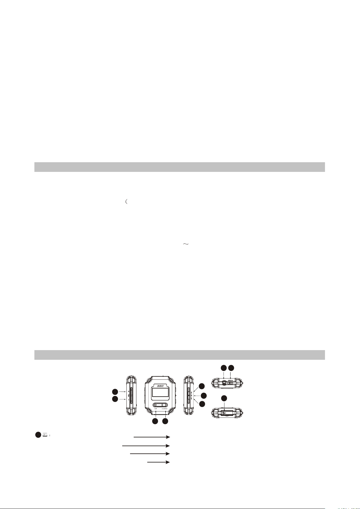
2.1.2 BUTTONS AND JACKS ILLUSTRATION
TM
5
4
M
1.1
# Press for long in any case
# Press in tuning mode
# Press in recording mode
# Press when operating in menu
6
7
1.3
1.1
1.2
3
2
8
enter main menu
switch in PRESET and SCAN mode
exit recording
not save the setup and return to the previous menu
- 4 -
Page 10
1.3
1.2
2
3
4
5
6
HOLD button: Push towards arrow to lock buttons; and push toward the opposite direction to
# Press in playback mode
# Press for long in playback mode
# Press in tuning Preset mode
# Press in tuning SCAN mode
# Press for long in tuning Preset mode
# Press for long in tuning SCAN mode
# Menu mode
# Press in power-off mode
# Press for long in power-on mode
# Press in playback mode
# Press in recording mode
# Press in tuning mode
# Press in menu mode
# Press for long in menu mode
# Press in playback mode
# Press for long when playing music file
(non recording file)
# Press in browsing file mode
# Press for long in tuning mode
# Press in Play and tune mode
# Press in
the next/previous track
fast forward/backward
select channel
manual scanning
full auto scanning
automanual scanning
move cursor or set item
power on
power off
pause playing
pause recording
pause (mute)
enter the selected item or
confirm the setup
enter recording mode
A-B repeat
switch
sound effect
delete file
Start FM recording
adjust volume
adjust dB value
unlock.
7
Headphone jack
8
USB jack
2.1.3 MAIN MENU ILLUSTRATION
# My music
Memorize music file.
# My Voice
Memorize microphone recording file,
such as meeting, classroom and
interview recording, etc.
# Resume Play
Select "Resume Play" and the player
begins to play from the position that
music stopped playing last time.
2.1.4 PLAYING INTERFACE ILLUSTRATION
1
Play State
2
Sound effect mode
3
Playback mode
4
Repeat state
5
Battery capacity
6
Song name and Singer
# REC
Select "REC"to enter recording
mode
# FM Radio
Select " FM Radio"to enter radio mode.
# System Setup
Select " System Setup" to set system items.
# System Setup
Select " System Setup" to set system items.
7
Time that has been played
8
Number of tracks
9
Spectrum display
- 5 -
Page 11
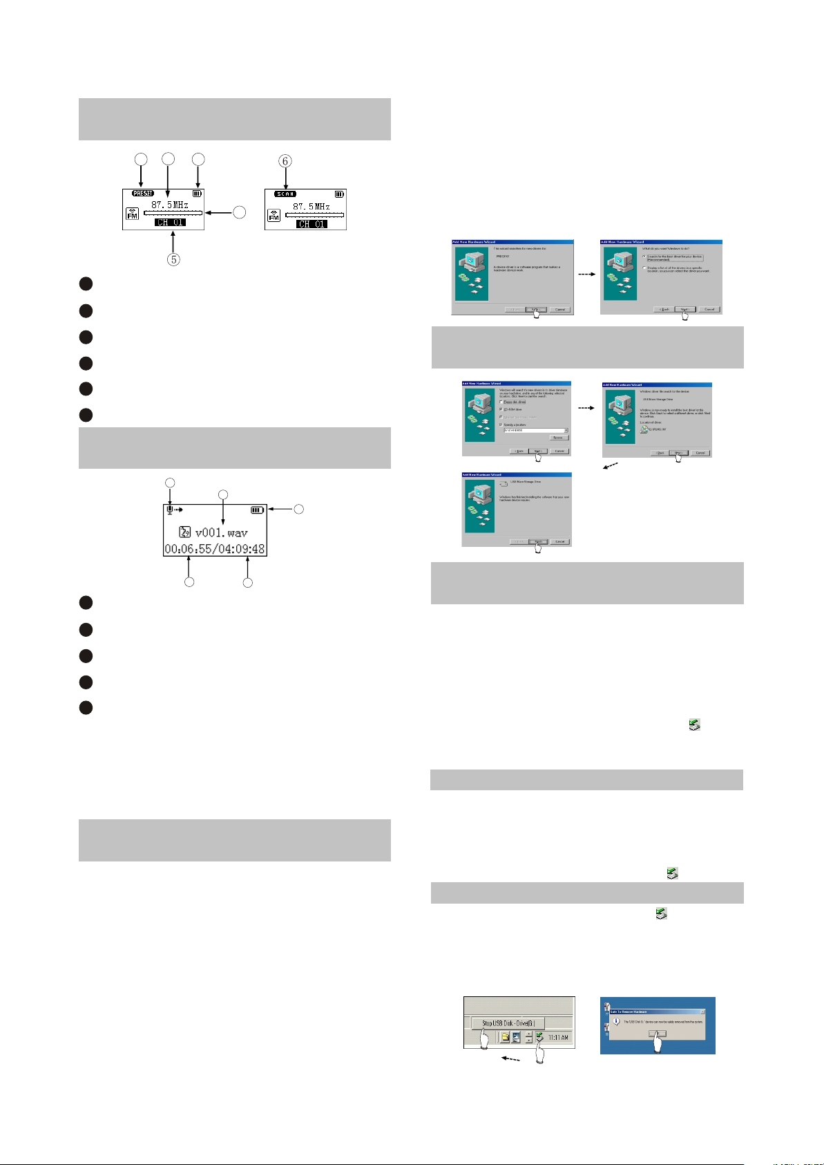
2.1.5 TUNING INTERFACE
ILLUSTRATION
2
1
1
PRESET mode (normal receiving)
2
Frequency of the current radio station
3
Battery capacity
4
Frequency bar
5
PRESET channel display
6
SCAN mode (scanning)
3
4
2.1.6 RECORDING INTERFACE
ILLUSTRATION
5
1
2
You only need to find the drive nformation file
on disc according to prompt information to
finish the installation of drive program.
3. After installation finishes, restart the computer
and you may use the mobile storage function
normally.
Shown as the following figure:
2.2.2 INSTALL USB DRIVE
PROGRAM
3
1
Name of recorded file
2
Battery capacity
3
Time that has been recorded
4
The left recordable time
5
Recording state
4
As for the name of recorded file
"V001.WAV": 001 is serial number of the current
recorded track and arranged according to
sequence; WAV is file format after recording
2.2 BASIC OPERATION
2.2.1 INSTALL USB DRIVE
PROGRAM
If your computer is Windows 98, you must
install drive program if you want to use the
mobile storage function of MP3 player in
computer.
1. Place USB drive disc into CD-ROM driver of
computer.
2. Connect MP3 player to computer will
automatically indicate that
new firmware device has been found, and run
the installation guide, shown as the following
figure.
2.2.3 USE MOBILE STORAGE
FUNCTION
This player can be used as mobile storage
in Windows ME/2000/XP operating system. In
Windows 98SE and Mac operating system, drive
program must be installed firstly and then used
as mobile storage. Connect Mp3 PLAYER and
computer with USB transmission line. After the
bottom right comer of desktop appears” “
symbol, the mobile storage function of Mp3
PLAYER may be used normally.
NOTE:
# To avoid abnormality of the player appears,
you are suggested to power off firstly before
connecting use USB transmission line to
connect Mp3 PLAYER, then connect computer.
# In Windows 98 system, there is no” “ symbol.
2.2.4 DISCONNECT USB SAFELY
After operation finishes, click” “ symbol
on bottom right corner of Windows desktop with
right button of mouse, and disconnect USB
safely according to the computer prompt.
- 6 -
Page 12
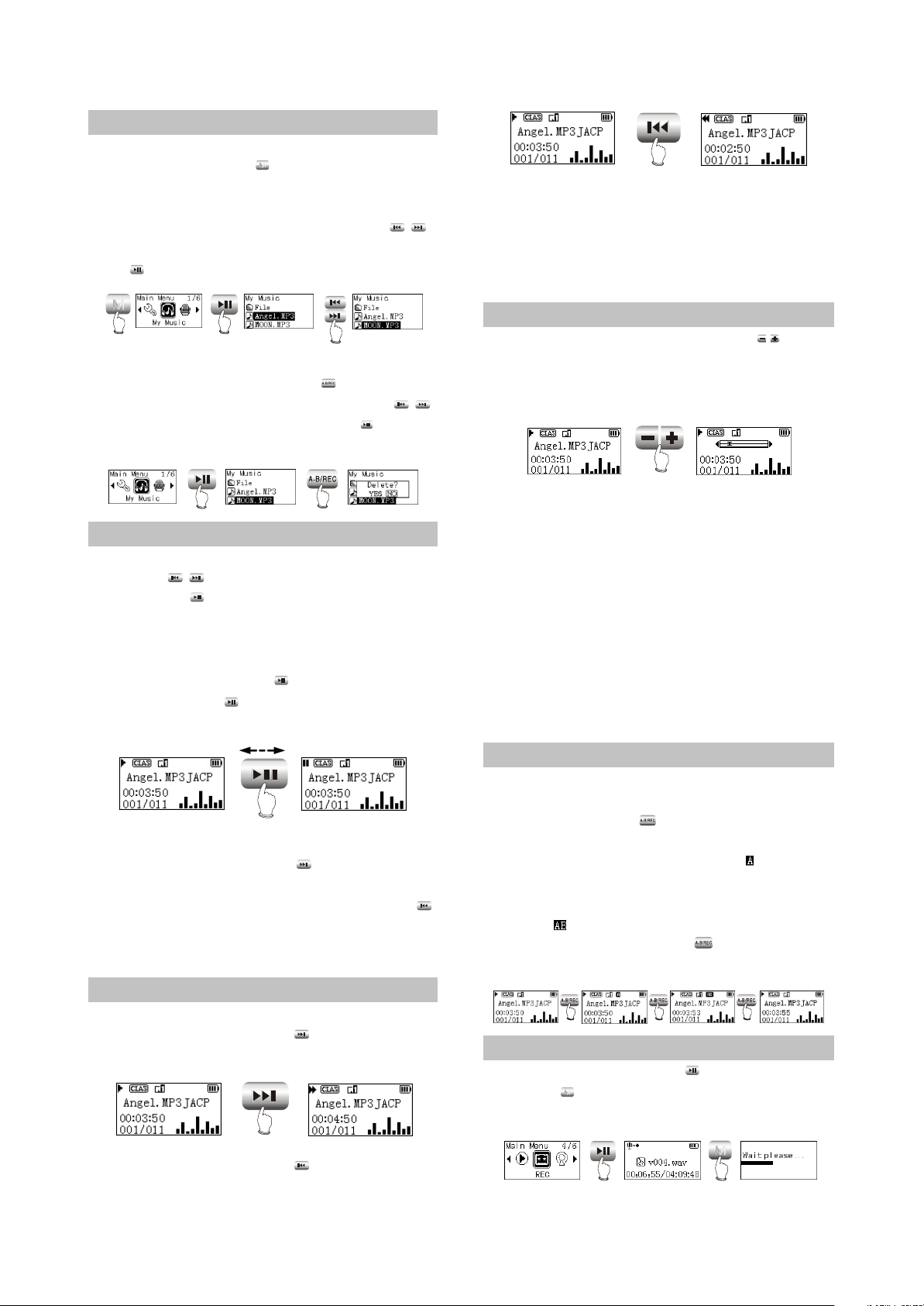
2.2.5 BROWSE/CANCEL FILE
# BROWSE FILE
In any case, press button for long to enter
"Main Menu". Music fileand recording file are
separately saved in the first two items of main
menu, "My Music" and "My Voice". Press
button to select upward or downward and then
press button to enter files browsing .
M
PRESS
FOR LONG
# CANCEL FILE
When browsing files, press button and
the cancel dialogue box will pop up. Press
button to select "YES" and then press button
to cancel the file. Select "NO" to exit.
M
/
PRESS
PRESS
/
PRESS
FOR LONG
CAUTION:
CAUTION:
Fast forward and fast backward operation
are only for the current track. After fast
backward/forward to the beginning/ending of
track, it switches into normal playback
automatically.
2.2.8 PLAY MUSIC
When playing or tuning, pressing button
or for long may adjust volume. The display of
adjusting volume in music playback interface is
shown as follows:
/
PRESS
PRESS
2.2.6 PLAY MUSIC
# PLAY MUSIC
press button to select song In "My
/
Music". Press button or select playback in
main menu to begin playing music, meanwhile
the playback interface displays.
# PAUSE PLAYING MUSIC
When playing, press button to switch to
pause state. Press button again to continue
playing.
PRESS
# NEXT and PREV
When playing, pressing button may skip
to the next track to play. If playback time of the
current track is less than 5 seconds, pressing
button may skip to the previous track to play,
otherwise the current track will be played again if
playback time is more than 5 seconds.
2.2.7 PLAY MUSIC
# FF and FB
When playing, pressing button for long
may realize fast forward.
PRESS
FOR LONG
CAUTION:
# Music playback will be paused when browsing
file.
# In some operating system (such as complex
font Windows), the operation of copying
lyrics/song file and changing song's name may
probably lead to incorrect display. When
playing WMA songs of VBR , pressing buttons
may probably has slow response or has no
lyrics display. When playing some non
standard songs or songs with special format,
noise may probably occur.
2.2.9 A-B REPEAT FUNCTION
When playing, if you want to listen to a
certain segment repeatedly, please use A-B
repeat function.Press button for the first time
to select the beginning point that you desire
to repeat play and screen displays " ";press it
for the second time to select the ending point
that you desire to repeat play and screen
displays " “, and system begins to repeat play
between A-B segment. Press button for the
third time to cancel repeat and continue to play.
PRESS PRESS PRESS
2.2.10 RECORDING
When recording, press button to pause
and press button for long to exit recording
and then make files.
M
When playing, pressing button for long
may realize fast backward.
- 7 -
M
PRESS
PRESS
FOR LONG
Page 13
CAUTION:
# To avoid sudden power-off when
recording, you cannot record when in low battery
and when disc is fully written. If you are
recording, it indicates "DISC FULL" and exits
recording.
# When recording with microphone, if you press
buttons and the sound of pressing may
probably be recorded.
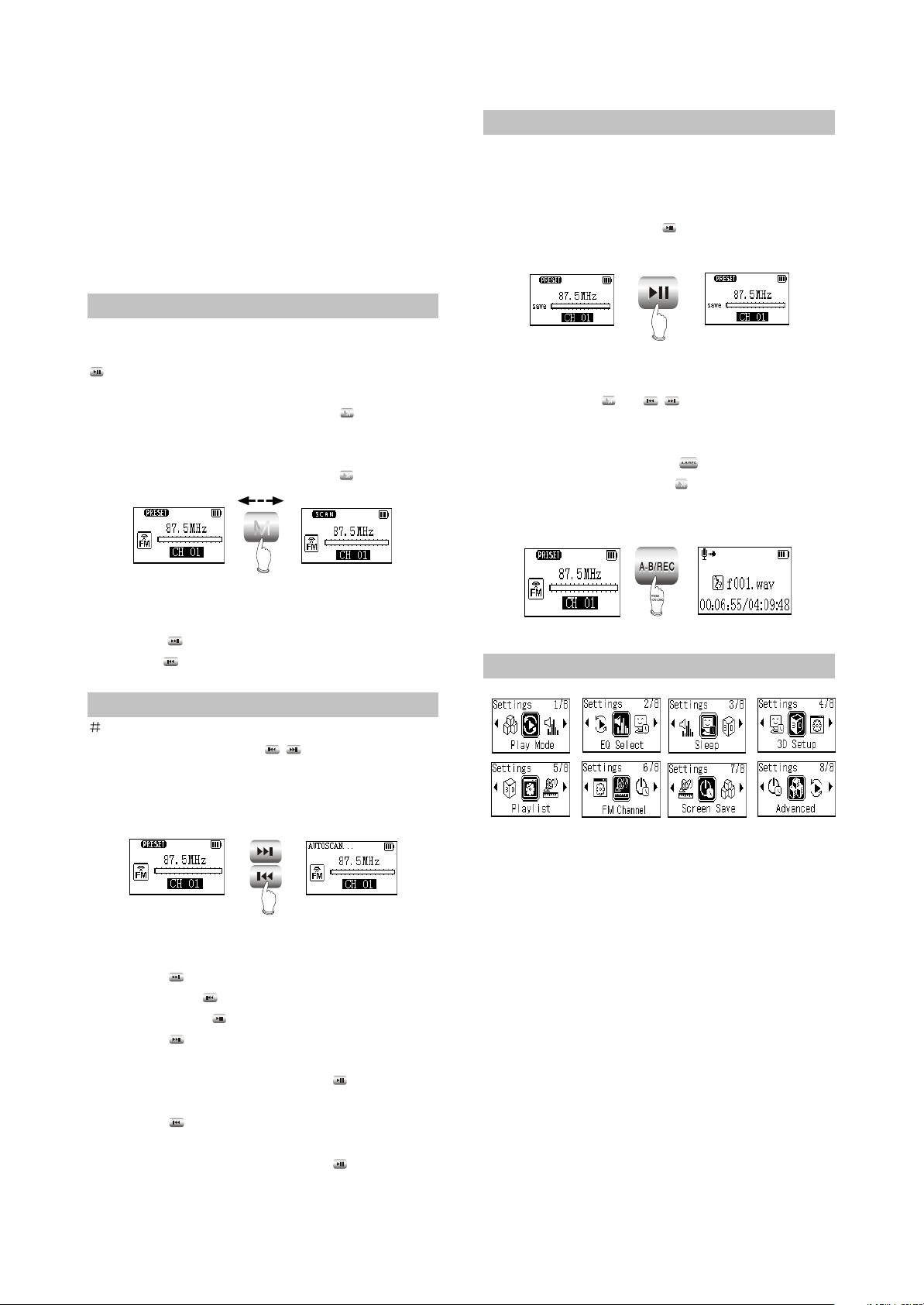
2.2.11 TUNING
# ENTER TUNING MODE
Select "FM Radio" in main menu and press
button to listen to radio.
# EXIT TUNING MODE
When listening to radio, press button for
M
long to return to main menu.
# PRESET/SCAN MODE SWITCH
When listening to radio, press button to
M
M
PRESS
2.2.13 TUNING
# SAVE RADIO STATION
Select channel in Preset mode firstly, and
then switch to SCAN mode to adjust frequency
(manually or automanually). After scanning
desired frequency, press buttonto save
into the current PRESET channel.
PRESS
CAUTION:
In the course of full auto/automanual
scanning, press or button to stop
M
scanning.
# FM RECORDING
In tuning mode, press button for long to
enter FM recording. Press button to stop
recording and make recording fil . FM recording
makes WAV format file.
/
M
1. PRESET mode
# ADJUST CHANNEL
Press button to enter the next channel,
and press button to enter the previous
channel.
2.2.12 TUNING
FULL AUTO SCANNING
PRESS
FOR LONG
/
In PRESET mode, press button for long to
begin full auto scanning. All
scanned radio stations will be saved in PRESET
channel automatically.
2. SCAN MODE
# MANUAL/AUTOMANUAL SCANNING
Press button to increase 0.1MHz each
time; and press button to decrease 0.1MHz
each time. Press button to save radio station.
Press button for long to increase
frequency continuously and stop until radio
station has been searched. Press button to
save radio station.
Press button for long to decrease
frequency continuously and stop until radio
station has been searched. Press button to
save radio station.
2.3 SETTINGS
2.3.1 SETTINGS
# Play Mode
Normal
Shuffle
Playlist
Intro
REP One
REP ALL
REP DIR
# EQ Select
Normal
3D
PURE
POP
Clas
Jazz
Rock
Dbass
Disco
My EQ
# Sleep
Disable120Min
# 3D Setup
BassBoost
ConcertSound
# Playlist
Browse
Edit
Delete
# FM Channel
Auto
Mono
# Screen Save
Disable - 5Min
- 8 -
Page 14
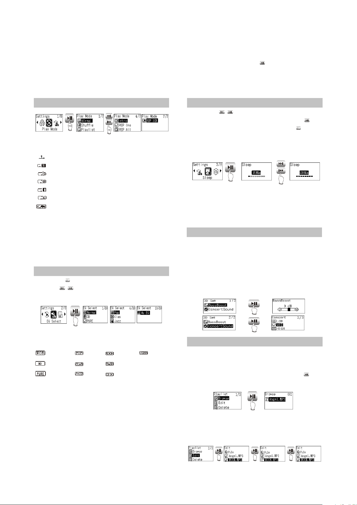
# Advanced
My EQ
REC Set
Format
Load Default
System Info
Language
2.3.2 PLAY MODE
The playback symbol displays on playback
interface is shown as follows:
Play according to track sequence.
random play any one track.
play the track edited in program list.
browse play each track for 10 seconds.
repeat play single track.
repeat play all tracks.
repeat play all tracks in this Folder.
CAUTION:
# Play mode is defaulted to "Normal" each time
when power on.
# Files in "My Voice" only support sequence
playback.
# When playing files in "My Voice", there is no
"Play mode" item.
2.3.3 EQ SELECT
Press button to enter "EQ SELECT", and
then use to move cursor, shown
as follows:
M
/
Mp3 player will switch to that in the cursor for the
moment to facilitate you to select your desired
sound effect mode. Press button to confirm
this sound effect mode.
CAUTION:
When playing files in "REC", there is no "EQ
Select " item.
2.3.4 SLEEP
Press button to adjust the timing
power-off time. After setup finishes, press
button to save and then exit, and press button
not to save and then exit. If timing power off time
is 15 minutes, after 15 minutes, MP3 PLAYER
will power off automatically.
CAUTION:
# It is defaulted to be invalid each time when
power on.
# Timing power-on time is a rough time, and may
have difference.
/
M
PRESS
PRESS
2.3.5 3D
In this menu, "3D “ may be adjusted.
BassBoost can strengthen bass effect; and
concert can build classical sound field effect. At
the same time of confirming clearness,
strengthen hearing feeling. Through adjustment,
you may feel live and vivid sound field
effect no matter where you are.
PRESS
The corresponding icons of each EQ mode
in playback mode are shown as follows:
NORMAL
3D
PURE
POP
CLAS
JAZZ
ROCK
DBASS
DISCO
My EQ
Select "3D", and correspond with 3D that
you have preset in "MAIN MENU->SYSTEM
SETUP->3D SETUP. If you have not set it, it is
default value.Select "MY EQ", and correspond
with the sound effect that you have preset in
"MAIN MENU->SYSTEM SETUP->ADVANCED".
If you have not set it, it defaults "MY EQ" to
NORMAL" sound effect.
When the cursor moves to a certain sound
effect mode, the sound effect mode played by
PRESS
PRESS
2.3.6 PLAYLIST
# Browse
Select "Browse" , and you may check how
many songs have been program-med into
playlist.When browsing playlist. Pressing
button may begin playing.
PRESS
Note: Playback will be paused when in
"Browse" or "Edit" list.
# Edit
PRESS PRESS PRESS
- 9 -
Page 15
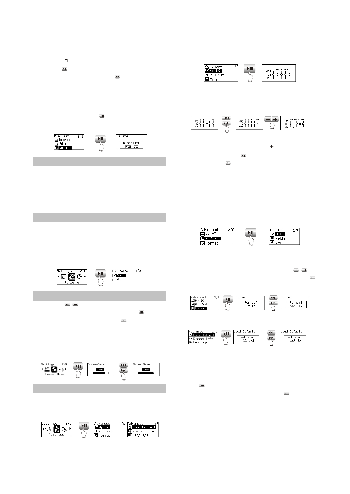
As in the above illustration, enter "Edit" and
browse files. The icon before songs in the
playlist is " “. Select a song not in the playlist
and press button to add it intothe list. Select a
song in the playlist ,and press button to cancel
it from the playlist,You can add 15 songs into the
playlist at most.
# Delete
Select "Delete". After dialogue box pops up,
select "YES", and press button to
confirm and the playlist is cleared.
PRESS
2.3.7 PLAYLIST
NOTE:
# If the operation of adding or cancelling music
files is detected, MP3 PLAYER will clear
the playlist automatically.
# You cannot enter "Edit list" and "Clear list"
when in program playback.
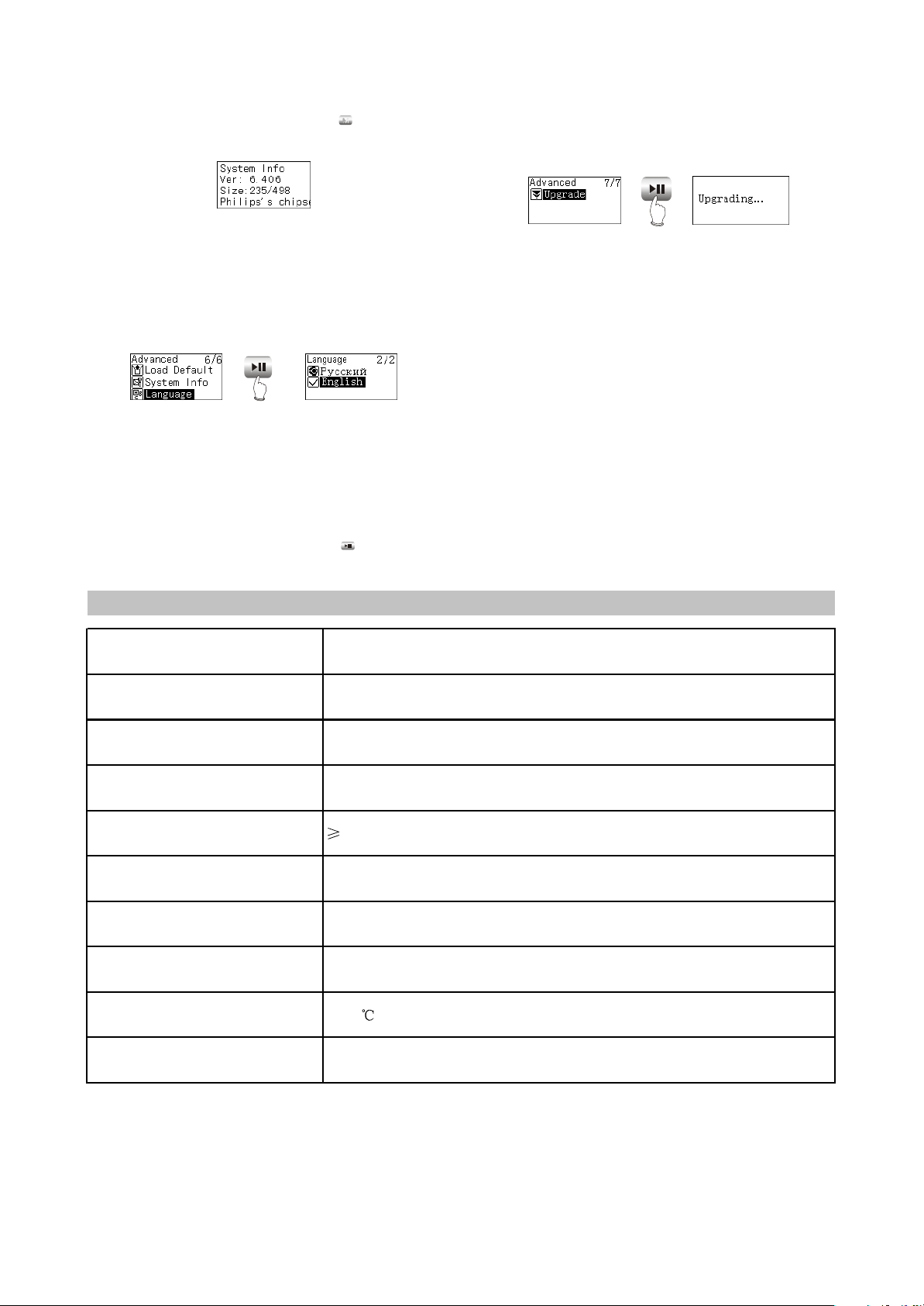
2.3.8 FM CHANNEL
You can select the FM channel in settings.
When select Auto, it changes the channel
automatically when in tunning mode. When
select Mono, it tunes at Mono channel all the
time.
PRESS
“My EQ" interface, you may see the decibel
(dB) of each frequency.
PRESS
If you want to adjust the decibel of mediant
(1kHz), operate according to the below
illustration.
PRESS
PRESS
When adjusting width, take 3dB as a step
and the max adjustable range is 15dB. After
setup finishes, press button to confirm and
exit, and press button to exit with the original
M
setup not being changed.
# REC Set
Here to set the recording quality ,The
recording quality is higher, the sound quality is
better and the used space is more. Three kinds
of recording quality adopt IMA-ADPCM
format coding.
PRESS
# Format
Enter this menu, and you may format hard
disk. When dialogue box pops up, press
/
button to move cursor to “YES”,and then press
button to confirm to finish formatting operation.
2.3.9 SCREEN SAVE
Press button to adjust the screen
saver time. After setup finishes, press button
to save and then exit, and press button not to
save and then exit. If the screen saver setup time
is 3 minutes and no operation occurs within 3
minutes, Mp3 PLAYER will enter screen saver
state automatically.
/
M
PRESS
PRESS
In
2.3.10 ADVANCED
Advanced items include some other system
internal setup, such as user sound effect setup,
default setup and system information.
PRESS
# My EQ
PRESS
PRESS
# Load Default
PRESS
PRESS
If you want to restore MP3 PLAYER to
factory setup state (data and song files cannot
be cancelled), you may select “ Load Default ”.
After dialogue box pops up, select “YES” ,
press button to confirm and then exit to restore
to default state. Select “NO” or press button to
M
cancel.
CAUTION:
Estore to "Default" state is effective only
when power on again.
# System Info
You may find information of firmware
version, total disc capacity and left disc capacity.
- 10 -
Page 16
In system information menu, press button to
Model X21
Audio dicode chip Philips PNX0101
Continuous playback time The longest time is about 10 hours
Dimensions/weight 57mm×45mm×14mm about 30.7g
Audio SNR
90dB
Headphone out 9mW+9mW(32ohm im pedance)
Frequency range 18Hz~20kHz
FM tuning rang 87.5MHz~108MHz
Working temperature
0~40
Files supported MPEG 1/2 Layer 3(16kbps~320kbps),WMA(8kbps~192kbps),WAV
M
return to the previous menu.
CAUTION:
Because firmware will use some space, the
displayed content capacity may probably be
different from the actual capacity.
# Language
Russian and English are supported.
PRESS
# Upgrade
Download the latest firmware upgrading file
from BBK website firstly, such as "BBK X21RU.
ebn" and "X21RU_Resource.bin", copy the two
files into MP3 PLAYER at the same time, and
then power on again. Find "Upgrade" item in
"ADVANCED" of "SETTINGS", and pressing
button may start upgrading.
After upgrading finishes, MP3 PLAYER will
power on again.
PRESS
NOTE:
# Only MP3 player detects that there is
upgrading file in system when this player
power on, "Upgrade" menu will appear in
"ADVANCED" item.
# Make sure MP3 PLAYER has enough quantity
of electric charge before upgrading.
# To ensure successful firmware upgrading, do
not power off during the course of upgrading.
# Upgrading will last about 10 seconds or more,
please try your best not to operate any buttons
during this course.
# After firmware upgrading finishes, some
function or interface may probably be different
from user manual, so please take real object
as standard.
2.4 SPECIFICATION
- 11 -
Page 17

Chapter Three Principle and Servicing
section One Principle of the Player
3.1.1 Function introduction and principle of the player
X21 (RU) portable MP3 player is composed of the following functional modules:
# MP3 main decode chip: main chip adopts PNX0101 decode chip of Philips Company, PNX0101 is
the professional MP3 decode IC of Philips Company, with ARM and DSP integrated inside. The
advantages are good sound quality and low power consumption.
# Power management module: composed of TPS79301, TPS62200 and PQ1X28 and responsible
for the power supply of each part of MP3.
# USB module: USB jack, data exchange, and charge function.
# Lithium battery module: power supply of the player.
# Memory module: data storage of the player.
# OLED module: display of the working state of the player.
# Headphone output: audio output.
# MIC: external audio input, which fulfills recording function.
# Tuningmodle: FM tuning.
3.1.2 Block diagram
Block diagram is shown in the figure 3.2.1.1:
USB jack
module
management
USB power
Charger power
Low voltage detect
Charge
management
ISL6294
S80821
5V
Power
TPS79301
TPS62200
3.6V~4.2V
Lithium battery
module
LDO
DC-DC
LDO
PQ1X28
G690L263T
12M crystal
oscillator
Reset IC
3.3V
1.8V
2.8V
OLED module
PNX0101
MIC
12.1V
DC-DC
LMS2703
Button and
switch control
circuit
Headphone
output
FLASH
Figure 3.1.2.1 Block diagram of X21 (RU)
- 12 -
MEMORY
FM module
TEA5767
Page 18
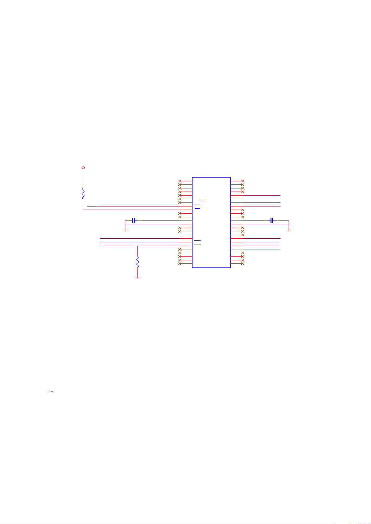
3.1.3 Introduction to IC used by the player
PCB board Location IC model Function
U1 TPS79301 Provide 3.3V voltage
U2 G690L263T System reset
U3 TPS62200 Provide 1.8V voltage
U4 ISL6294 Charge management
U5 S80829 Low voltage detect
U6 Philips PNX0101 MP3 decode
U7 PQ1X28 Provide 2.8V voltage
U8 TC58512FT Flash Memory
U9 SI912DL Headphone mute
Tuning board
U1 TEA5767HN Tuning module
Mian board
Introduction to IC used by X21 (RU ) is shown in the following figure:
- 13 -
Page 19
Section Two Unit Circuit Principle
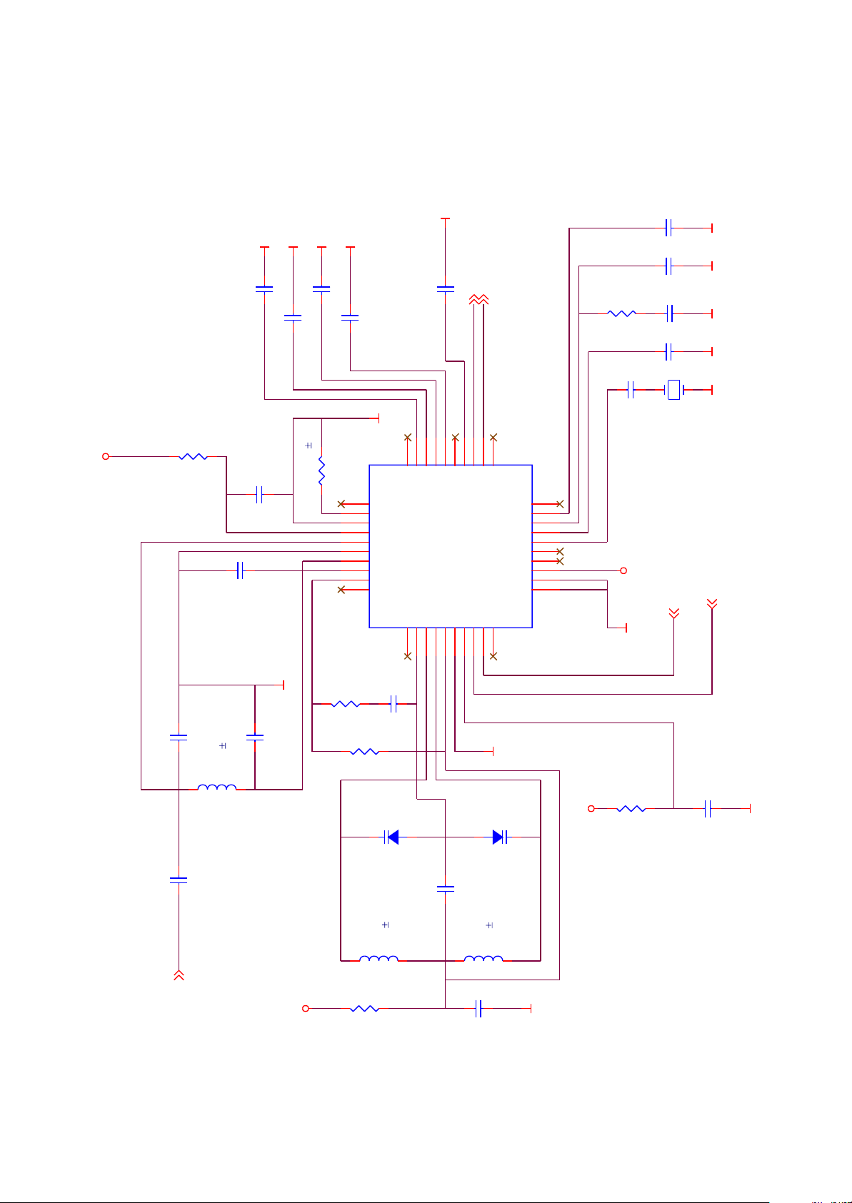
3.2.1 FLASH circuit principle
1. FLASH circuit schematic diagram is shown in the following figure 3.2.1.1:
FLASH3V3
TC58512FT
U1
R1
100K
/RE
/CE
CLE
ALE
/WE
/WP
1
NC
2
NC
3
NC
4
NC
5
NC
6
GND
7
RY/BY
8
RE
9
CE
10
C2
104
D_GND D_GND
R2
100K
FLASH3V3
NC
11
NC
12
Vcc
13
Vss
14
NC
15
NC
16
CLE
17
ALE
18
WE
19
WP
20
NC
21
NC
22
NC
23
NC
24
NC
NC
NC
NC
NC
I/O8
I/O7
I/O6
I/O5
NC
NC
NC
Vcc
Vss
NC
NC
NC
I/O4
I/O3
I/O2
I/O1
NC
NC
NC
NC
48
47
46
45
44
43
42
41
40
39
38
37
36
35
34
33
32
31
30
29
28
27
26
25
MPMC_AD7
MPMC_AD6
MPMC_AD5
MPMC_AD4
FLASH3V3
MPMC_AD3
MPMC_AD2
MPMC_AD1
MPMC_AD0
C1
104
D_GND
Figure 3.2.1.1 Flash circuit schematic diagram
2. Working principle: Flash Memory is the storage unit of the player and all Mp3 and waveform files
must be saved in FLASH. Flash module is composed of FLASH chip TC58512FT and peripheral circuit,
which fulfills the read, write and cancel working of internal files. In whic
h, 601 magnetic L15, 104
capacitor C45 and C46 compose FLASH power filtering circuit and provide FLASH with pure 3.3V
voltage. R38 is p
ull-up resistor of /CE, R40 is pull-down resistor of /WP, Vcc is power supply pin of
FLASH, /CE is chip selection signal, VCC33 provides 3.3V voltage and FLASH begins to work. /RE, /WE
are effective read and effective write signal end respectively to control read and write function of FLASH.
I/O1 I/O8 is 8 data lines to fulfill the exchanges of FLASH and external data.
3.2.2 FM module circuit
1. FM module circuit schematic diagram is shown in the figure 3.2.2.1:
2. Working principle: FM module is composed of microwave digital tuning IC TEA5767HN produced
by Philips Company and the peripheral circuit, in which, L17, C54, C55 is the power supply filtering
circuit of FM module that provides IC with the pure voltage with typical value 2.8V. Cn1 is the socket
between FM module and main board.
- 14 -
Page 20
C1, C2, C3, C4, L1 is the antenna input matching circuit of FM module; variable capacitance diode
D1, D2 and winding inductor is the frequence selection tuning circuit in FM module. The control of FM
adopts IIC bus control means, 9 and 10 of TEA5767 are two control input ends.
SGND
SGND
SGND
C6 473
C7 473
R1
10R
FM_3V3
C5
475/X5R/0603
C3
472
SGND
SGND
FM_OUTL
C8 473
C9 333
SGND
U1
R2 18K 1%
31
32
33
34
35
36
37
38
39
40
29
30
N.C
N.C
IFGAI
AGND
AVCC
RFI1
RFGND
RFI2
TCAGC
LOOPSW
N.C
N.C
CPOP2VCOT13VCOT24VCOVCC5DGND6DVCC7DATA8CLOCK9N.C
1
DIFL128DIFL2
FM_OUTR
C12 333
FM_OUTL
FM_OUTR
21
22
23
24
26
27
N.C
LAVO
MPXO25VREF
RAVO
TCIFC
TMUTE
NECTAR-IO603CS
TEA5767HN
N.C
20
PHLF
19
PDLF
18
XTAL2
17
XTAL1
16
SWP2
15
SWP1
14
BUSEN
13
BUSM
12
W/R
11
10
R6
33K
C14
102
C18
C17
223
C16
223
SGND SGND SGND
C15
22PF
102
D-GND D-GND
XT1
32.768KHz
FM_3V3
D-GND
IIC_SDA 2
IIC_SCL 2
C10
R3
SGND
C4
C2 27PF
C1 101
FM_ANT
FM_ANT3
47PF
L1
120nH/ 2%
FM_3V3
10K
R5
R4
393
100K
D-GND
C19
104/X5R/0402
BB202
D1
C11 103
33nH 2%
O603CS
L2
22R
BB202
D2
L3
33nH 2%
SGND
C13
104/X5R/0402
dandu
FM_3V3
R7
22R
D-GND
Figure 3.2.2.1 FM module circuit schematic diagram
- 15 -
Page 21
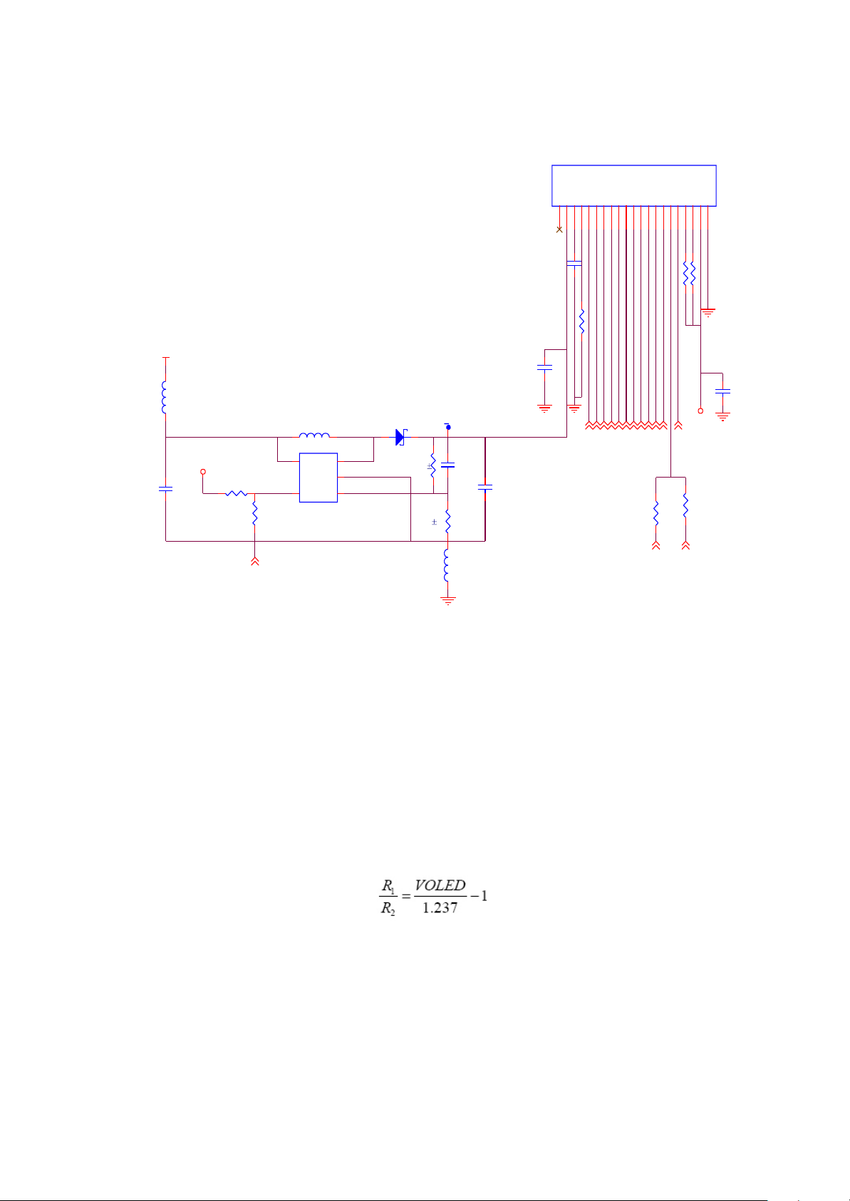
3.2.3 OLED module circuit
1. OLED module circuit schematic diagram is shown in the figure 3.2.3.1:
CN4
NC1VCOMH
VCC
3
2
4
IREF
D7
5
D5
D3
D66D48D2
7
9
VDD
D/C#
WR#
RES#16RD#
D1
D0
11
12
10
BS2
CS#17GND21BS1
20
15
14
13
18
19
C71
475/X5R/6.3V
P_VDD
L24
601
VCC33
R71
100K
EN1
CDRH3D16-4R7
5
4
R73
0R
L25
1
VIN
SW
2
GND
3
EN
FB
U10
TPS61040/LM2703
D8
MBR0520/SOD123
240K 1%
R70
27K 1%
VOLED
C68
22P
L26
0R
GND
Figure 3.2.3.1 OLED circuit schematic diagram
C65
16V/104
C72
106/25V/1206
C63
103
VOLED
R65
2M
LCD_DB72LCD_DB3
LCD_DB62LCD_DB5
R63
R64
4.7K
4.7K
GND
C67
2
2
2
2
2
2
2
LCD_DB12LCD_DB4
LCD_DB2
R74
0R*R75
2
LCD_WR
LCD_D/C2LCD_DB0
LCD_CS
LCD_RD
/RESET
104
LCD_3V3
R72
0R
_RESET
2. Working principle: for 12V high voltage is required to lighten OLED, boosted circuit must be used
togther to fulfill it and the circuit includes two parts: boosted circuit and OLED jack circuit. In which,
boosted circuit is composed of boosted DC-DC LM2703 and peripheral circuit, VIN is power input, EN is
the enable end of LM2703, high level is effective, SW is high voltage output pin, FB is feedback pin, the
voltage value VOLED outputted by high voltage is achieved through selection the two divider resistance
and they satisfy the following relationship:
Seen from the above, VOLED is about, 12.2V. L25, C72 in circuit are energy storage inductor and
output capacitor of boosted circuit.
OLED jack circuit is connected with OLED jack of PNX0101 directly, the internal program of
PNX0101 controls the characters display of OLED, working state information of the player is displayed
through OLED to fulfill man-machine communication.
- 16 -
Page 22
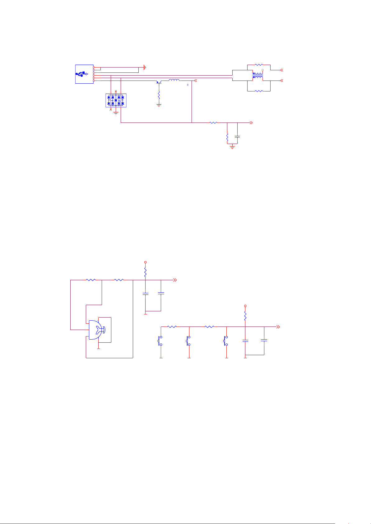
3.2.4 USB jack circuit
1. USB jack circuit schematic diagram is shown in the figure 3.2.4.1:
USB1
3DU05S-32T-10
Shield
Shield
GND
VB+
6
5
4
3
D+
2
D-
1
4
5
D5
362
1
GND
GND
Q8
L18
GND
R44
1K
680 DCR<100m
SS8550LT
RC LAMP0504FC
USB_VBUS 2
R47 100K
R42 18R
13
R43 18R
USB_DET 1
24
T1
SDCW2012-2-900T
USB_DP 2
USB_DM2
180K
R49
C56
104
Figure 3.2.4.1 USB jack circuit schematic diagram
2. Working principle: USB jack network is composed of VB+ (USB 5V power), D+ (anode data line),
D -( cathode data line) and GND (ground line). In the circuit, PNP triode Q8 is reverse insert protection
function to prevent the damage of Mp3 internal circuit because of reverse insert; D5 is TVS diode array
used for anti - static.
3.2.5 Button circuit
1. Button circuit schematic diagram is shown in the figure 3.2.5.1:
MENU
R55
300R
PREVIOUS
1
T
2
NEXT
D_GND
R56
220R
5C
PREVIOUS
S1
VCC33
D_GND
R54
1K
C57
104
A-B/REC
KEY_SCAN_2 2
C58
SFI0402-050E100NP
R68
750R
S3
VOL- C70
D_GNDD_GND D_GND
R69
510R
S4
S5
VOL+
VCC33
R67
D_GND
1K
SFI0402-050E100NP
C69
104
KEY_SCAN_1 2
Figure 3.2.5.1 Button circuit sche0matic diagram
2. Working principle: buttons of X21 (RU) include a 3-direction button, a HOLD switch and 4 single
buttons (in which one is ON/OFF and PLAY button and will be introduced in ON/OFF circuit). Button
detection uses partial voltage mode, which utilizes ADC circuit of PNX0101 to check voltage value of the
preset button to determine which button functions, then make the corresponding reaction by internal
program to fulfill function of each button.
To lock button, directly use a IO port of PNX0101 to detect high and low level. When high level is
detected, lock is determined, other buttons do not function. C58, C70 and C73 are voltage dependent
resistor to prevent ESD.
- 17 -
Page 23
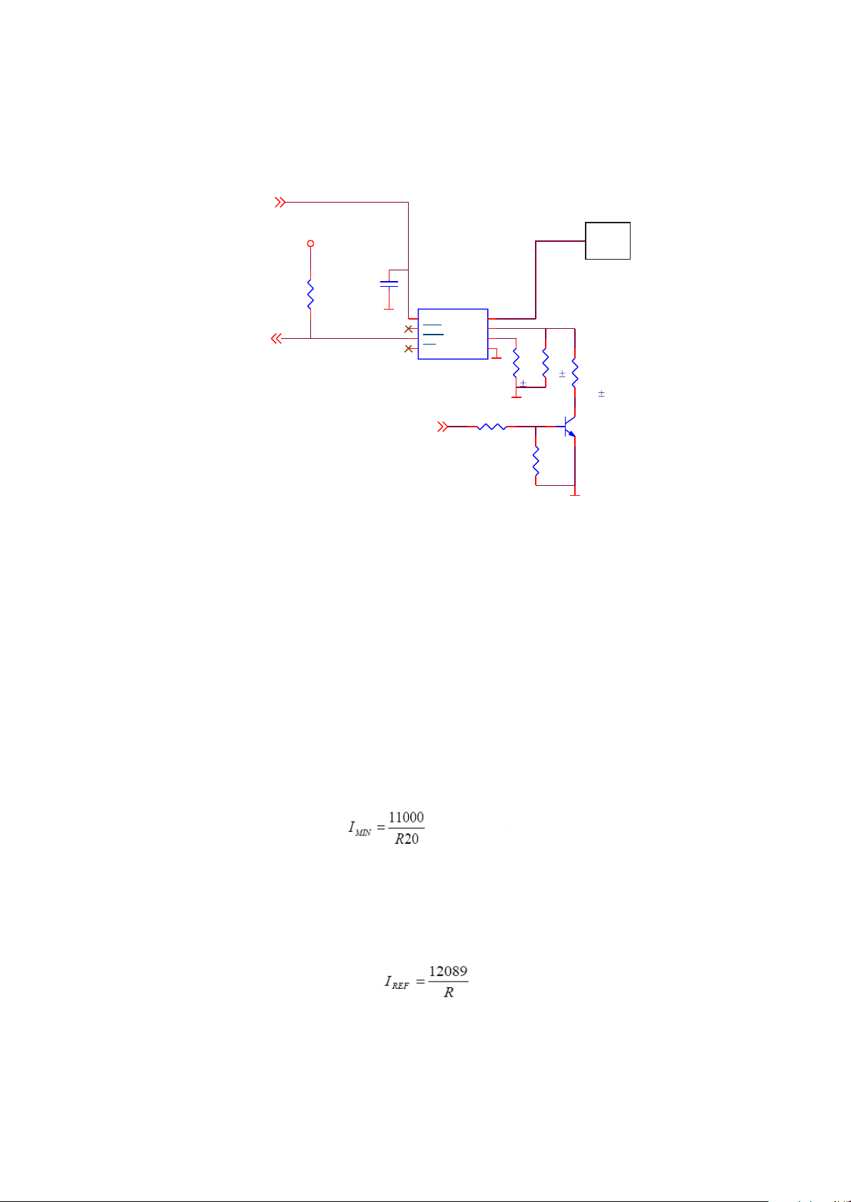
3.2.6 Charge management circuit
1. Charge management circuit mainly charges lithium-ion battery and the circuit schematic diagram
is shown in the figure 3.2.6.1:
USB_VBUS
/STATUS
VCC33
R16
47K
C12
105/X5R
P_GND
U4 ISL6294
1
IN
2
PPR
3
CHG
EN4GND
I_SET
BAT
IREF
IMIN
P_GND
R25 10K
8
7
6
R20
5
510K 1%
P_GND
R21
120K 1%
R26
100K
BAT
R22
120K 1%
Q6
SS8050LT
P_GND
3.2.6.1 Charge management circuit schematic diagram
2. Working principle: seen from the circuit, charge circuit is mainly fulfilled by charge control IC
ISL6294 and peripheral circuit. IN pin is power input pin of ISL6294, that is the input end of USB 5V, BAT
is output pin of ISL6294, that is the input end of lithium battery; /CHG is charge state indication end,
when /CHG is in low level, it means the charge is in process, on the contrary it means the charge is
finished; IMIN is minimum charge current setup end, that is, when charge current is less than the
current value set by this end, charge is stopped. The setup of minimum charge current is fulfilled through
selecting external resistor R20. The relationship between Minimum charge current IMIN and R20 is
shown as follows:
(MA)
Seen from the above, minimum charge current is about 20 milliampere.
IREF is setup end of charge current, ISL6294 uses this reference current to charge lithium battery.
The relationship between charge current I and resistor connected externally:
REF
Triode Q6 in circuit is used for charge current selection. When users use computer to charge battery,
PNX0101 outputs I_SET, which is low level, Q6 cuts off, and R21 is connected into circuit. Seen from the
above, I is about 100 milliampere; when users use charger to charge battery, PNX0101 outputs I_SET,
EFR
which is high level, Q6 is Saturated on, R21 and R22 are connected into circuit in parallel, seen from the
- 18 -
Page 24

Above, I is about 200 milliampere. The reason why we design like this is that USB jack of some
REF
computers (such as laptop computer) cannot provide large current to charge battery.
3.2.7 Low voltage detecting circuit
1. Function of low voltage detecting circuit is that when input voltage of he player is detected to be
lower than a certain voltage value, the player turns off. Low voltage detecting circuit schematic diagram
is shown in the figure 3.2.7.1:
P_GND
S80829CN NB /S1000N29-N4T1/R3111Q291AT1S
EN
R18 33K
C15
102*
P_GND
U5
VSS
1
RST
VDD2NC
R24
100K
P_VDD
4
3
Q4
P_GND
MMST3906
R15
470K
VCC33
R10
100K
P_GND
Figure 3.2.7.1 Low voltage detecting circuit schematic diagram
2. Working principle: low voltage detecting ciorcuit is fulfilled by IC S80829CNNB and PNP triode
Q4. S80829CNNB is high precision voltage detector detect valve value is 2.9V and precision is +2 .
P_VDD is he input voltage of the player, when P_VDD is lower than 2.9V, RST pin of IC outputs low level,
pin triode Q4 is saturated on, control level output is low level which cuts off the power pf the player to
power off.
3.2.8 Battery protection circuit
1. Battery protection board is installed on lithium battery and used to protect lithium battery from
being damaged by short circuit, over discharge and over charge. Lithium battery and battery protection
board are all lithium battery core components by us. Circuit schematic diagram of battery protection
board is shown in the figure 3.2.8.1:
figure 3.2.8.1 Battery protection circuit diagram
- 19 -
Page 25

Battery protection circuit equivalent circuit diagram is shown in he figure 3.2.8.2:
P+
R1
LITHIUM BATTERY
C1
5
Ct
Vss
VDD
U1
Dout
1
U2
V-
Cout
3
C3
2
R2
P-
4
B
6
C2
Figure 3.2.8.2 Battery protection circuit equivalent circuit schematic diagram
2. Working principle: battery protection circuit is mainly composed of battery protection IC S8261
and built-in dual N groove MOSFET ECH8601. S8261 is lithium-ion polymer of built-in high precision
voltage detect circuit and delay circuit, which may be served as protection IC of battery. DOUT and
COUT pin are over-discharge (when lithium battery voltage is lower than 2.4V, it is called over discharge)
protection output end and over-charge (when lithium battery voltage is higher than 4.2V, it is called over
charge) protection output end. When in normal condition, these two pins are high level, MOSFET
switches on, lithium battery voltage outputs to the player through protection board; when in protection,
these two pins output low level to control MOSFET and turn off power. Over-current detection (short-
circuit protection) is fulfilled through detecting short corcuit stat
e by V- pin to control DOUT and COUT
output. When battery has short circuit, voltage on V- externally connected resistor has a sudden change,
V- dete
cts that voltage on R2 increases instantly to control DOUT and COUT to output low level at the
same time and control MOS tube to cut off from battery to protect battery.
3.2.9 Power management module
1. Function of power management module is to provide the player with 3.3V, 3.8V and1.8V of
normal working. Circuit schematic diagram is shown in the figure 3.2.9.1, 3.2.9.2 and 3.2.9.3:
P_VDD
C2
106/X5R
P_GND
R3
68K
1
2
TPS7930 1
P_GND
EN
U1
VIN
VOUT
GND
EN3BYPASS
T
S
O
C6
102
FB
23-6
C4
103
6
5
R1
33K1 %
4
C1 22PF
R2
20K 1%
VCC33
VCC33
C3
106/X5R
P_GNDP_GND
Figure 3.2.9.1 3.3V power circuit schematic diagam
- 20 -
Page 26

VCC33
PQ1X281M2ZP
1
VI
2
C39
106/X5R C40
GND
EN3BYPASS
VOUT
U7
5
4
C41
104
D_GND
R4
300K¡À1%
R5
120K¡À1%
P_GND
P_VDD
P_GND D_GND
Figure 3.2.9.2 2.8V power circuit schematic diagram
U3
C8
106/X5R
1
VI
2
GND
3
EN
TPS62200 /FAN5307*
P_GNDP_GND
EN
SW
FB
5
4
T
23
S
O
L1
CDRH3D16/HP-100
-
5
106/X5R
C7
47PF
C10
101
VCC18
2.8V
C9
106/X5R
VCC18
Figure 3.2.9.3 1.8V power circuit schematic diagram
2. Working principle: seen from the figure 3.2.9.1, 3.3V power is supplied by IC TPS79301 and
peripheral circuit. TPS79301 is a linear voltage stabilizing module (LDO also called), EN pin is
theenable pin that controls normal working, high level is effective; BYPASS has a resistor inside that can
composes low pass filter together with external 103 capacitor C4 to decrease output noise; the setup of
TPS79301 output voltage is decided by the resistance value of the two externally-connected resistors of
FB pin and the relationship is shown as follows:
Seen from the above, VOUT is about 3.2V.
1.8V power of the working of the player is provided by IC TPS62200 and peripheral circuit.
TPS62200 is high efficiency voltage drop DC-DC converter. EN is enable pin and high level is effective.
The relationship between TPS62200 output voltage and FB pin feedback resistor is shown as follows:
Seen from the above, the output voltage is about 1.75V.
To improve sound quality of Mp3 and effect of FM and microphone, we introduce 2.8V power to
supply power for audio system of PNX0101 and FM and microphone, feature of this channel 2.8V power
is: it is outputted by LDO PQ1X281, power is very pure with low ripple voltage. PQ1X281 may output
fixed voltage 2.8V, EN is the enable end.
- 21 -
Page 27

3.2.10 Headphone jack circuit
1. Headphone jack circuit schematic diagram is shown in the figure 3.2.10.1:
GND
142
RCLAMP0504FC
R51
0R
1
3
4
5
2SJ-A382-001(HP-AC)
CN3
D6
3
U9
1
S1
2
G1
3
D2
Si1912DLS
6
D1
5
G2
4
S2
FM_ANT
OUTROUTL
FM_ANT
L27 106
L29 106
L28 106
6
5
R521KR53
1K
HP_VOUTR2
HP_VOUTL 2
R57 4.7K
R58
47K
MUTE 2
C59
103
Figure 3.2.10.1 Headphone jack circuit schematic diagram
2. Working principle: left and right channel audio signals outputted from PNX0101 output through
being coupled by 220uF capacitor to headphone jack circuit. Headphone jack circuit is composed by
dual MOS tube SI1912DL that controls sound output and headphone socket CN3, pin 2 and pin 5 of
SI1912DL are connected to mute circuit, after pressing MUTE button the control dual MOS tube is
cracked to cut off the output of headphone left and right channels. D6 is circuit is TVS diode array and
used to protect ESD. Ground wire of headphone is also served as the antenna input of FM module.
3.2.11 Reset circuit
1. Reset circuit supplies rest signal to PNX0101. Reset circuit schematic diagram is shown in the
figure 3.2.11.1:
VCC33
U2
G690L263T71/R3111N252CT1
2
GND
VCC
RESET
3
1
R76
0R
P_GND
/RESET 2,3
C5
SFI0402-050E100NP
P_GND
Figure 3.2.11.1 Reset circuit schematic diagram
2. Working principle: reset circuit is composed by reset IC G690L263 . G690L263 may output a low
level reset pulse signal with 140 millisecond pulse width to reset the player. C5 in the circuit is voltage
dependent resistor and used to protec ESD.
- 22 -
Page 28

3.2.12 ON/OFF control circuit
1. ON/OFF control circuit schematic diagram of X21 (RU) is shown in the figure 3.2.12.1:
P_VDD
R13
5.6M
P_GND
R8
10K
47K
R19
2M
START
R9
10K
D4
1N4148WSR14
START 3
START
OFF 2
PLAY/PAUSE2
START1
C62
SFI0402-050E100NP
SFI0402-050E100NP
PLAY
P_GND
C64
VCC33
Q2
MMST3906
R10
100K
EN
R15
470K
P_GND
1N4148WS
Q3
SS8050LT
D3
R17
100K
Q5
MMST3904
R12
100K
C14
475/X5R
R23 1M
VCC33
R62
100k
D7
1N4148WS
L23
601/1005
S2
START/PLAY/PAUSE
D_GND
PLAY/PAUSE
Figure 3.2.12.1 ON/OFF control circuit schematic diagram
2. Working principle: ON/OFF control is fulfilled through operating ON/OFF button S2 bu users.
When press S2 to power on, S2 is connected, START sends out low level signal, Q2 is saturated on,
battery voltage P_VDD makes EN high level through Q2, R12 and D3 to make power management
module work, power system of the player starts and machine power on; when power off normally (for
instance, press ON/ONN button for a long time or battery electric charge is too low), PNX0101 sends out
OFF high level to make Q3 saturated on to pull EN down to ground, power management module stops
working and machine power off; when accidents happens, system fails, PNX0101 has not any reaction
to any operation, now press S2 and Q2 is saturated on all the time, battery voltage P_VDD charges C14
through Q2, R13 and R19, when C14 is charged higher than 0.5V, Q3 is on, EN is low level and the
player power off. PN knot of R17 and Q5 is the figure is the discharge loop of C14.
3.2.13 MIC circuit
1. MIC circuit schematic diagram is shown in the figure 3.2.13.1:
ADC_VDDA33
R59
100K
R60
470K
Q9
MMST3904
C60
106
R61
2.2K
MIC1
C61
ADC_MIC
MICROPHONE
104
Figure 3.2.13.1 MIC circuit schematic diagram
- 23 -
ADC_MIC 2
Page 29

2. Working principle: MIC circuit is mainly composed of microphone and microphone power biasing
circuit. MIC1 switches the recorded external voice signals to electrical signal, through C61 coupling,
output to ADC circuit of PNX0101 to converse analog electric signal to digital electric signal and form
WAV files after encoding of software to save in FLASH.
In the circuit, R59, R60, Q9 and C60 are triode voltage stabilizing system, which provides stable
power bias for microphone, R61 is the bias resistor of microphone.
- 24 -
Page 30

Section Three Servicing Cases
3.3.1 Servicing cases
Example 1 Symptom: power not on
Description: no screen display and no output
Analysis and troubleshooting: firstly check whether this trouble is caused by battery or by power
circuit, connect to power adapter and check whether charge is available and whether screen has display.
Power on and there is no display, check power supply 3.3V and 1.8V and find that 3.3V lowers to 0.6V,
and voltage in normal working condition should be 1.8V, 3.3VDC-DC switch circuit is shown in the figure
3.3.1.1, use power adapter to supply power, 5V input is normal, charge enable end is high level, which is
also normal, observe carefully and find that pin 6 of Ic9301 has false welding, after welding again trouble
is removed.
P_VDD
C2
106/X5R
P_GND
R3
68K
P_GND
EN
U1
1
VIN
2
GND
EN3BYPASS
TPS79 30 1
C6
102
VOUT
S
O
T
FB
23-6
C4
103
6
5
4
R2
20K 1%
R1
33K1 %
C1 22PF
VCC33
P_GNDP_GND
C3
106/X5R
VCC33
Figure 3.3.1.1 3.3VDC-DC switch circuit schematic diagram
Example 2 Symptom: machine not switched on
Description: no screen display, no response after pressing ON/OFF button
Analysis and troubleshooting: firstly confirm whether it is machine not switched on or it is power not
on, connect to adapter or computer and check whether display on screen is normal, connect to adapter
and charge can display, which means that power and rear stage circuit working are basically normal,
ON/OFF circuit is shown in the figure 3.3.1.2 , the working principle is that after a light touch switch S2
closes, a loop appears and s signal Start produces, triode Q2 is on and gives a enable signal to power
control, test S2 switch, press down and check whether it is on, during test we find that S2 has false
welding. After welding again, trouble is removed.
- 25 -
Page 31

P_VDD
EN
100K
R15
470K
VCC33
R10
P_GND
D3
1N4148WS
Q3
SS8050LT
R17
100K
Q5
MMST3904
Q2
MMST3906
R12
100K
C14
475/X5R
R23 1M
R13
5.6M
P_GND
R8
10K
47K
R19
2M
R9
10K
START
D4
1N4148WSR14
START 3
START
OFF 2
Figure 3.3.1.2 ON/OFF circuit schematic diagram
Example 3 Symptom: computer not connected
Description: when connecting to computer, no reaction and o screen display
Analysis and troubleshooting: firstly confirm whether charge and power on are available, and the
result is normal. Use diode position of multimeter and anode of pen to ground, test whether the
resistance value to ground of D+, D- data signals in the position of USB terminal is close to several
hundred omh, short-circuit could not appear between D+ and D, when testing we find that D+ is normal,
D- resistance value is infinite, USB terminal has false welding. After welding again, trouble is removed.
Example 4 Symptom: only one side of headphone has output
Description: only one side of headphone has output and the other has not.
Analysis and troubleshooting: firstly decide the trouble lies in tuning components or in common part,
whether only one side has sound when listening and result is normal. Tuning circuit is shown in the
figure 3.3.1.3, tuning part components reaches the main board through a flat cable holder, radio station
program can be received and this shows that power supply, data and clock are all normal, use
oscillograph to test left and right channel output of FM directly and find that FM-OUTL has no waveform
output, then check tuning board output part and waveform is normal, circuit at back is connected through
a flat cable holder, press the flat cable holder and it is ok, after losing, trouble appears again, so we
decide that flat cable holder has trouble, after changing it trouble is removed.
CN1
IIC_SDA
IIC_SCL
IIC-SDA
IIC-SCL
D_GND
CON2X4
FM_3V3
6 5
8 7
12
34
FM_ANT
FM-OUTL
FM-OUTR
FM_OUTL
FM_OUTR
Figure 3.3.1.3 Tuning circuit schematic diagram
- 26 -
Page 32

Example 5 Symptom: noise when playing
Description: headphone output has noise when playing music
Analysis and troubleshooting: if noise appears when playing, it is generally the condition that BGA
has trouble, functions, such as playing are all normal and only noise appears, so we need to analyse the
trouble is caused by decode part or rear stage. Headphone output part circuit is shown in the figure
3.3.1.4. When playing 1KHZ standard signal, it should be sine wave signal, and not any clutter exists.
Firstly test C32 and waveform in C33, and there exists clutter, so we decide that BGA has trouble, after
changing it trouble is removed.
C27 332
C28 332
HP_VOUTR2
HP_VOUTL2
C31 220UF/4V
C32 220UF/4V
R29 10RC40 104
M3
M2
P3
N3
N2
N1
DAC-VOUTR
DAC-VOUTL
HP-OUTR
HP-OUTL
HP-OUTCA
HP-OUTCB
DAC
Figure 3.3.1.4 Decode part circuit schematic diagram
Example 6 Symptom: charge is not available
Description: connect to charger, charge displays, but low electric charge displays when power on
after charge finishes.
Analysis and troubleshooting: as for this trouble, charge mode displays, charge also displays, but
full charge is not available, machine cannot power on after charging for 3 hours, power on after
unplugging charge line and low electric charge displays and machine power off automatically. Charge
management circuit diagram is shown in the figure 3.3.1.5, machine can enter charge mode and there is
charge indication, which means that there is power input, BAT and CHG are normal, so you should
consider charge control pin, check IMIN current control end mainly, when current of this pin is small,
charge stops, when checking this end, we find that R20 is false welding; after welding again, trouble is
removed.
USB_VBUS3
VCC33
R16
47K
/STATUS2
C12
105/X5R
P_GND
U4 ISL6294
1
IN
2
PPR
3
CHG
EN4GND
I_SET
BAT
IREF
IMIN
P_GND
R25 10K
8
7
6
R20
5
510K 1%
P_GND
R21
120K 1%
R26
100K
BAT
R22
120K 1%
Q6
SS8050LT
P_GND
Figure 3.3.1.5 Charge board circuit schematic diagram
- 27 -
Page 33

Example 7 Symptom: no screen display
Description: screen is not on and there is no display
Analysis and troubleshooting: firstly confirm the trouble appears in power supply and screen itself,
after power and listen, the sound is normal, so we preliminarily decide that power supply 3.3V, 1.8V are
basically normal. Screen display control circuit is shown in the figure 3.3.1.6. Test voltage on two ends of
L25 and it is about, which is normal, then test voltage on two ends of D8 and find that anode has no 13V,
remove screen and there is still no13V. Check input end voltage and enable end is basically normal,
then check feedback pin FB voltage and it is on low side obviously, and capacitor C68 also has trouble.
After changing it, trouble is removed.
CN4
VDD
NC1VCOMH
VCC
2
D5
IREF
D66D48D2
D7
7
3
4
5
D39WR#
D1
D0
13
11
12
10
D/C#
RES#16RD#
BS2
CS#17GND21BS1
20
15
14
18
19
P_VDD
L24
C71
475/X5R/6.3V
601
VCC33
R71
100K
EN1
2
CDRH3D16-4R7
5
4
R73
0R
L25
1
VIN
SW
2
GND
3
EN
FB
U10
TPS61040/LM2703
MBR0520/SOD123
Figure 3.3.1.6 Screen display control circuit schematic diagram
Example 8 Symptom: screen trouble
Description: screen display has error and disorder
D8
R70
240K 1%
27K 1%
VOLED
C68
22P
L26
0R
GND
C65
16V/104
C72
106/25V/1206
C63
103
VOLED
R65
2M
2
LCD_DB72LCD_DB3
LCD_DB62LCD_DB5
R63
R64
4.7K
4.7K
GND
C67
2
2
2
2
2
2
LCD_WR
LCD_DB12LCD_DB4
LCD_D/C2LCD_DB0
R74
0R*R75
LCD_CS
LCD_RD
/RESET
LCD_DB2
104
2
LCD_3V3
R72
0R
LCD
2
1,2
_RESET
Analysis and troubleshooting: servicing of screen trouble is similar to that of no screen display and
the difference is that power supply may not be considered, that is, power supply should be normal.
Firstly confirm the trouble lies in screen itself or the circuit, change display screen and trouble still exists,
then use oscillograph to test 8-bit data on OLED display screen, we find during the test that flat cable
holder of display screen is false welding, after welding again trouble is removed.
Example 9 Symptom: noise when recording
Description: when playing record files, there is noise.
Analysis and troubleshooting: recording circuit is shown in the figure 3.3.1.7 and composed of
microphone and microphone biasing circuit.
- 28 -
Page 34

MIC switches the recorded external voice signal to electric signal, through C61 coupling, output to
ADC circuit of Pn0101 and form WMV files after being coded by software to save in Flash. Firstly lay
sound file and check whether there is noise, and there is no, check recording circuit, power supply is
normal, when recording, use oscillograph to test C61 and there is clutter interference. After changing
MIC, trouble is removed.
ADC_VDDA33
R59
100K
R60
470K
Q9
MMST3904
C60
106
MIC1
MICROPHONE
R61
2.2K
C61
104
ADC_MIC
ADC_MIC 2
Figure 3.3.1.7 Recording circuit schematic doagram
Example 10 Symptom: computer cannot be connected
Description: after connecting to computer, hardware cannot be found
Analysis and troubleshooting: movable disc of computer cannot be found, when this trouble
appears, checjk whether you may upgrade software and download program to upgrade. Open DFU
program, download firmware again and it is ok. Note: firmware of Mp3 need to be upgraded always.
When meets this trouble, trouble is removed.
- 29 -
Page 35

3.3.2 Troubleshooting flow chart
1. Troubleshooting process for “No screen display” is shown in the figure 3.3.2.1:
No screen display
Whether
12V voltage of D8 cathode
is normal
Y
Whether
there is 12V voltage on
display screen
socket
Y
Change
display screen
components and check
whether it is
normal
Y
Display screen has trouble
N
Check DC-DC boosted
circuit and elements around
N
Whether display screen flat
cable holder has false welding
N
Display screen flat
cable holder has trouble
Figure 3.3.2.1 Screen display circuit troubleshooting figure
- 30 -
Page 36

2. Troubleshooting process for “USB not connected” is shown in the figure .3.3.2.2:
USB not connected
whether
5V of L18 is normal;
whether grounding is
normal
Y
Whether 3.3V, 1.8V
are normal
Y
whether
oscillation of 12M
crystal oscillator is
normal
Y
check
resistor to ground of
D+, D-
Y
Change audio decode
IC PNX0101
N
Q8 has trouble or USB
socket has false welding
N
Check each DC-DC switch
circuit and peripheral elements
N
Change crystal oscillator or
capacitor on two sides
N
Check whether T1 or USB
socket pin has rosin joint
Figure 3.3.2.2 USB jack troubleshooting flow chart
- 31 -
Page 37

3. Troubleshooting process for “Button has no function” is shown in the figure 3.3.2.3:
Button has no function
Whether
all functions have no
function
Y
whether
lock button has
action
Y
HOLD
and 3.3V are
short-circuited ?
Y
Change HOLD button
N
Change some button
N
N
Change BGA
Change BGA
Figure 3.3.2.3 Button circuit troubleshooting flow chart
- 32 -
Page 38

4. Troubleshooting process for “Charge is not available”is shown in the figure 3.3.2.4:
Charge is not available
Whether
battery voltage is fully
charged 4.2V-4.3V
Y
Battery
full charged, protected?
Y
Discharge is ok
Figure 3.3.2.4 Charge management circuit troubleshooting flow chart
N N
Battery components have
trouble
Charger
and computer cannot
charge?
Y
whether
power supply is normal?
Y
Whether
BAT voltage has
variation
Y
Check I_SET and whether
voltage high level is normal
N
Check power supply circuit
N
Change IC6298
- 33 -
Page 39

5. Troubleshooting process for “Power not on” is shown in the figure 3.3.2.5:
Power not on
Check U3 and circuit
around
Whether
3.3V output is normal
N
Whether
1.8V output is normal
Check BGA working
conditions
N N
Y
N
Y
Whether
5V input is normal
Whether
load is too heavy
Y
BGA has trouble
N
Check U1 and circuit around
Figure 3.3.2.5 Power management circuit troubleshooting flow chart
Check whether Q8 is
normal
- 34 -
Page 40

6. Troubleshooting process for “Machine not switched on” is sown in the figure 3.3.2.6:
Machine not switched on
N
Whether adapter is
charged
Y
Refer to troubleshooting
flow chart for "Power not on”
Whether
S2 has open circuit and
false welding
Y
Change S2
Figure 3.3.2.6 ON/OFF control circuit troubleshooting flow chart
N
Whether Q2 is normal
Whether D8 is on
Check whether EN end is
normal
N
Check whether 3.3V power
Y
Y
supply of R10 is normal
N
Check whether R12 or D3
has open circuit
- 35 -
Page 41

Section Four Servicing Parameters
3.4.1 Key point waveform diagram
This section collects signal waveform diagram of audio, video and each unit circuit with the purpose
to help servicing personnel to judge where trouble lies in accurately and quickly to improve servicing
skills. For the difference of oscillograph’s type, model and tuner, a certain difference may exist, so the
servicing personnel are expected to pay more attention to check in daily operation.
1. 12M crystal oscillator oscillation waveform diagram
2. L25 boosted energy storage waveform diagram
- 36 -
Page 42

3. L1 1.8V energy storage waveform diagram
4. LCD_CS wabeform
5. LCD_D/C waveform diagram
- 37 -
Page 43

6. LCD_RESET
7. LCD_WR waveform diagram
8. LCD_RD waveform diagram
- 38 -
Page 44

9. LCD_DB0 waveform diagram
10. LCD_DB1 waveform diagram
11. LCD_DB2 waveform diagram
- 39 -
Page 45

12. LCD_DB3 waveform diagram
13. LCD_DB4 waveform diagram
14. LCD_DB5 waveform diagram
- 40 -
Page 46

15. LCD_DB6 waveform diagram
16. LCD_DB7 waveform diagram
17. IREF waveform diagram
- 41 -
Page 47

18. VCOMH waveform diagram
- 42 -
Page 48

3.4.2 Key point voltage list
Test point
Working voltage (V
FM3V3 CN1_4
2.82
CN4_2 12.36
CN4_3 (screen bright) 9.58
CN4_4 9.46
CN4_20 3.31
VCC33 (one end of R62) 3.31
U8_9 3.28
U8_12 3.31
U8_19 3.31
Q9_C 3.31
Q9_B 2.65
Q9_E 2.06
MIC_+ 1.71
KEYSCAN_1_S3 1.09
KEYSCAN_1_S4 1.12
KEYSCAN_1_S5 0
- 43 -
Page 49

Section Five Function Introduction to IC
3.5.1 Function introduction to PNX0101
The PNX0101 (ARM-based Solid State Audio IC) is an IC based on an embedded RISC processor. The
device is designed for hand -held Solid State Audio applications like portable MP3 players. The high level of
integration, low power consumption and high processor performances make the PNX0101 very suitable for
portable hand-held devices.
The PNX0101 is based on the powerful ARM7TDMI CPU core, which is a full 32 -bit RISC processor with
8 k byte dedicated cache.
Pin function of PNX0101 is shown as the following table:
PIN Main Description
T10 XTALH_IN 12M clock in
V9 XTALH_OUT 12M clock out
U9 XTALH_VDDA18 Crystal oscillator analog power supply
T9 XTALH_VSSA Crystal oscillator analog ground
V7 XTALH_IN Digital ground
T8 XTALH_OUT Unused
U8 XTALH_VDDA18 Crystal oscillator analog power supply
V9 XTALH_GNDA Crystal oscillator analog ground
T12 SPDIF_IN Unused
U11 SPDIF_VDDA18 Grounding
T11 SPDIF_GNDA Grounding
U5 ADC10B_GPA 4 Unused
T6 ADC10B_GPA3 Unused
U6 ADC10B_GPA2 Unused
T7 ADC10B_GPA1 Unused
U7 ADC10B_GPA0
V10 ADC10B_VDDA33 10bitADC power supply
U10 ADC10B_GNDA 10bitADC grounding
-44 -
Analog common pin (battery+)
Page 50

M3 DAC_VOUTR AC grounding
M2 DAC_VOUTL AC grounding
L1 DAC_VDDA33 DAC analog power supply
L2 DAC_VREFP
M1 DAC_VREFN Grounding
P3 HP_OUTR Headphone output (right)
N3 HP_OUTL Headphone output (left)
N2 HP_OUTCA N1 connected
N1 HP_OUTCB N2 connected
R1 HP_VDDA33A Headphone analog power supply
R2 HP_VDDA33B Headphone analog power supply
P2 HP_GNDAA Headphone analog ground
P1 HP_GNDAB Headphone analog ground
T3 ADC_VCOM AC grounding
U2 ADC_VREFP Voltage reference
V1 ADC_VREFN Grounding
V3 ADC_VDDA18 Analog 1.8V power supply
U3 ADC_VDDA33 Analog 3.3V power supply
V2 ADC_GNDA Grounding
U1 ADC_VREF AC grounding
T1 ADC_VINR
T4 ADC_VINL
R3 ADC_MIC Analog input— MIC input
T2 ADC_MIC_LNA
G2 LCD_RW_WR LCD read/write gating
F2 LCD_E_RD
E3,E2,D3,D1,D2,C3
C1,C2
B3 LCD_CSB Chip selection
LCD_DB_7~0
Analog input (right)-tuning right
Analog input (left)-tuning left
LCD data line
F3 LCD_RS Data/instruction gating
J3 MCI_DAT_3 Card read gating
J1 MCI_DAT_2
J2 MCI_DAT_1 Unused
-45 -
Page 51

H3 MCI_DAT_0 Power off level
G3 MCI_CLK Card read chip selection clock
H2 MCI_CMD Unused
T15 USB_CONNECT_N USB2.0 output
U17 USB_DP USB data line
T17 USB_DM USB data line
U14 USB_VBUS USB power supply
P16 USB_RREF Unused
R17 USB_GNDA Analog
R16 USB_VSSA_REF Analog
T16 USB_VSSA_TERM Analog
U15 USB_VDDA18_PLL Unused
U16 USB_VDDA18_BG Unused
U18 USB_VDDA33 Unused
V18 USB_VDDA33_DRV Unused
H17 DAI_BCK Unused
G17 DAI_WS Unused
G16 DAI_DATA Unused
F16 DAO_CLK Unused
G18 DAO_BCK Unused
F18 FAO_WS Unused
F17 DAO_DATA Unused
T13 JTAG_TRST_N J1
V4 JTAG_TCK J2
U12 JTAG_TMS 3.3V
T5 JTAG_TDI J3
U13 JTAG_TDO J4
U4 JTAG_SEL_ARM J5
H16 IIC_SCL Serial clock IIC control
J17 IIC_SDA Serial data IIC control
B8,C8,B7,C7,B6,C6 MPMC_D_15~ 0
C5,C4,B5,A5,B4,A4
MPMC_A_20~ 0 MPMC address line
A3,B2,A2,A1
MPMC data in/out (use 7~0 as data line)
-46 -
Page 52

B11 MPMC_STCS_2 Unused
A8 MPMC_STCS_1 Unused
C9 MPMC_STCS_0 Unused
B9 MPMC_DYCS Unused
A10 MPMC_CLKOUT Unused
B10 MPMC_CKE Unused
C11 MPMC_WE Unused
A9 MPMC_RAS Unused
C10 MPMC_CAS Unused
A11 MPMC_DQM_1 Unused
C12 MPMC_DQM_0 Unused
A17 MPMC_NOE Read gating
B12 MPMC_BLOUT_1 Unused
A12 MPMC_BLOUT_0 Write gating
B1 MPMC_RPOUT Unused
L3 UART_TXD Unused
K3 UART_RXD Unused
K2 UART_NCTS Unused
K1 UART_NRTS Unused
J16 GPIO_3 DFO
K18 GPIO_2 G2
K17 GPIO_1 G2
K16 GPIO_0 P_GND
T14 RSTIN_N System reset
V15 FLASH_VDD_HV
H1 VDDI1 Merm core power supply
V11 VDDI2 Core power supply
V16 VDDI3 Flash core power supply
G1 VSSI1 Merm core grounding
V12 VSSI2 Core grounding
V17 VSSI3 Flash core grounding
E1 VDDE1 3.3V power supply
V5 VDDE2 3.3V power supply
-47 -
Page 53

V14 VDDE3 3.3V power supply
J18 VDDE4 3.3V power supply
A16 VDDE5
A7 VDDE6
F1 VSSE1 Grounding
V6 VSSE2 Grounding
V13 VSSE3 Grounding
H18 VSSE4 Grounding
A15 VSSE5 Grounding
A6 VSSE6 Grounding
L17 DCDC_PLAY Power on signal
L18 DCDC_STOP P_GND
N17 DCDC_LX2 DC- DC in
P17 DCDC_LX1 DC- DC in
T18 DCDC_VUSB USB voltage input
M17 DCDC_VBAT Battery power supply
1.8V~3.3V power supply
1.8V~3.3V power supply
R18 DCDC_VOUT33A DC/DC 3.3V out
M16 DCDC_VOUT33B DC/DC 3.3V in
N18 DCDC_VOUT18 DC/DC 1.8V in
P18 DCDC_VSS1 DC/DC grounding
N16 DCDC_VSS2 DC/DC grounding
L16 DCDC_GND Core grounding
M18 DCDC_CLEAN Datum circuit grounding
3.5.2 Function introduction to G690
The G690 are microprocessor (UP) supervisory circuits used to monitor the power supplies in??and
digital systems. They provide excellent circuit reliability and low cost by eliminating external components and
adjustments when used with +5V, +3.3V, +3.0V - powered circuits.
These circ uits perform a single function: they assert a reset signal whenever the VCC supply voltage declines
below a preset threshold, keeping it asserted for at least 140ms after VCC has risen above the reset threshold.
Reset thresholds suitable for operation with a variety of supply voltages are available.
-48 -
Page 54

Pin function is shown as the following figure:
Pin Contiguous signal name Function description
1 /RESET Output reset low level
2 VCC IC power supply
3 GND rounding
3.5.3 Function introduction to PQ1X281
PQ1X281 may output fixed voltage 2.8V, EN pin is enable end, high level works. The feature of the 2.8V
voltage outputted by this IC is small ripple and pure voltage, which is used to supply power for audio system,
FM and microphone.
Pin function is shown as the following figure: :
Pin Contiguous signal name Function description
1 VIN DC input
2 GND Grounding
3 EN Enable end
4 BYPASS Form filtering circuit with external resistor
5 VOUT Voltage output
3.5.4 Function introduction to TC58512FT
Offered in 512M×8bit, the K9K4G08U0M is 4G bit with spare 128M bit capacity. Its NAND cell provides
the most cost-effective solution for the solid state mass storage market. A program operation can be
performed in typical 200µs on the 2112-byte page and an erase operation can be performe d in typical 2ms on
a 128K -byte block. Data in the data page can be read out at 30ns cycle time per byte. The I/O pins serve as
the ports for address and data input/output as well as command input. The on-chip write controller automates
all program and erase functions including pulse repetition, where required, and internal verification and
margining of date Even the write-intensive systems can take advantage of the K9K4G08U0M's extended
reliability of 100K program/erase cycles by providing ECC(Error Correc ting Code) with real time mapping-out
algorithm. The K9K4G08U0M is an optimum solution for large nonvolatile storage applications such as solid
state file storage and other portable applications requiring non -volatility. An ultra high density solution having
two 4Gb stacked with two chip selects is also available in standard TSOPI package.
-49 -
Page 55

Pin function is shown as the following figure:
Pin Contiguous signal name Function description
9 /CE Chip selection
8 /RE Read gating
18 /WE Write gating
19 /WP Write protection
7 RY/BY Busy/idle judgment
12、37
VCC Power supply
3.5.5 Function introduction to SI1912DL
SI1912DL integrates 2 MOS tubes insides and is used to control on/off of two circuits. In X17 (RU),it is
served as control IC of secondary output.
Pin function is shown as the following figure:
Pin Contiguous signal name Function description
1 S1 S electrode of MOS tube 1
2 D1 D electrode of MOS tube 1
3 G2 G electrode of MOS tube 2
4 S2 S electrode of MO tube 2
5 G2 G electrode of MOS tube 2
6 D1 D electrode MO tube 1
3.5.6 Function introduction to LM2703
The LM2703 is a micropower step -up DC/DC in a small 5-lead SOT-23 package. A current limited, fixed
off-time control scheme conserves operating current resulting in high efficiency over a wide range of load
conditions. The 21V switch allows for output voltages as high as 20V. The low 400ns off-time permits the use
of tiny, low profile inductors and capacitors to minimize footprint and cost in space-conscious portable
applications. The LM2703 is ideal for LCD panels requiring low current and high efficiency as well as white
LED applications for cellular phone back-lighting. The LM2703 can drive up to 4 white LEDs from a single
Li-Ion battery.
-50 -
Page 56

Pin function is shown as the following figure:
Pin Contiguous signal name Function description
1 SW Voltage output end
2 GND Grounding
3 FB Output feedback
4 EN Enable end
3.5.7 TPS79301
The TPS793xx family of low-dropout (LDO) low-power linear voltage regulators features high power
supply rej ection ratio (PSRR), ultralow noise, fast start-up, and excellent line and load transient responses in
NanoStar wafer chip scale and SOT23 packages. NanoStar packaging gives an ultrasmall footprint as well as
an ultralow profile and package weight, making it ideal for portable applications such as handsets and PDAs.
Each device in the family is stable,with a small 2..2-µF ceramic capacitor on the output. The TPS793xx family
uses an advanced, proprietary BiCMOS fabrication process to yield extremely low dropout voltages (e.g., 112
mV at 200mA, TPS79330). Each device achieves fast start-up times (approximately 50µs with a 0.001-µF
bypass capacitor) while consuming very low quiescent current (170 µA typical). Moreover, when the device is
placed in standby mode, the supply current is reduced to less than 1 µA.
Pin function is shown as the following figure:
Pin Contiguous signal name Function description
1 VIN Voltage input
2 GND Grounding
3 EN IC enable pin
4 BYPASS Internal resistor and external compose filtering circuit
5 FB Feedback
6 VOUT Voltage output
3.5.8 Function introduction to TPS62200
The TPS6220x devices are a family of high-efficiency synchronous step-down converters ideally suited
for portable systems powered by 1-cell Li-Ion or 3-cell NiMH/NiCd batteries. The devices are also suitabl e to
operate from a standard 3.3-V or 5-V voltage rail. With an output voltage range of 6.0 V down to 0.7 V and up
to 300 mA output current, the devices are ideal to power low voltage DSPs and processors used in PDAs,
pocket PCs, and smart phones. Under nominal load current, the devices operate with a fixed switching
-51 -
Page 57

frequency of typically 1 MHz. At light load currents, the part enters the power save mode operation; the
switching frequency is reduced and the quiescent current is typically only 15 µA; therefore it achieves the
highest efficiency over the entire load current range. The TPS6220x needs only three small external
components. Together with the tiny SOT23 package, a minimum system solution size can be achieved. An
advanced fast response voltage mod e control scheme achieves superior line and load regulation with small
ceramic input and output capacitors.
Pin function is shown as the following figure:
Pin Contiguous signal name Function description
1 VIN Voltage input
2 GND Grounding
3 EN IC enable pin
4 FB Output feedback
5 SW External device pin, voltage output
3.5.9 Function introduction to ISL6294
The ISL6294 is a cost-effective, fully integrated high input voltage single-cell Li -ion battery charger. The
charger uses a CC/CV charge profile required by Li -ion batteries. The charger accepts an input voltage up to
28V but is disabled when the input voltage exceeds the OVP threshold, typically 6.8V, to prevent excessive
power dissipation. The 28V rating eliminates the over-voltage protection circuit required in a low input voltage
charger.
The charge current and the end-of-charge (EOC) current are programmable with external resistors. When
the battery voltage is lower than typically 2.55V, the charger preconditions the battery with typically 20% of the
programmed charge current. When the charge current reduces to the programmable EOC current level during
the CV charge phase, an EOC indication is provided by the CHG pin, which is an open-drain output. An
internal thermal foldback function protects the charger from any thermal failure.
Two indication pins (PPR and CHG) allow simple interface to a microprocessor or LEDs. When no
adapter is attached or when disabled, the charger draws less than 1µA leakage current from the battery.
Pin function is shown as the following figure:
Pin Contiguous signal name Function description
1 IN Power input
2 /PPR Charge voltage limit end
3 /CHG Charge state indication
-52 -
Page 58

4 /EN IC enable pin
5 GND System grounding
6 IMIN Minimum current setup
7 IREF Charge current setup
3.5.10 Function introduction to S80829
The S-808xxC series is a series of high -precision voltage detectors developed using CMOS process. The
detection voltage is fixed internally with an accuracy of ±2.0%. Two output forms, Nch open-drain and CMOS
output, are available. Ultra -low current consumption and miniature package lineup can meet demand from the
portable device applications.
Pin Contiguous signal name Function description
1 RST Control signal voltage output pin
2 VDD Voltage input pin
3 NC Unused
4 VSS Grounding
3.5.11 Function introduction to TEA5767HN
The TEA5767HN is a single -chip electronically tuned FM stereo radio for low-voltage application with fully
integrated IF selectivity and demodulation. The radio is completely adjustment-free and only requires a
minimum of small and low cost external components. The radio can be tuned to the European, US and
Japanese FM bands.
Pin function is shown as the following figure:
Pin Contiguous signal name Function description
1 NC Unused
2 CPOP
3 VCOT1 Tuning output voltage oscillator 1
4 VCOT2 Tuning output voltage oscillator 2
5 VCOVCC Tuning oscillator power supply
6 DGND Digital ground
7 DVCC Digital power supply
-53 -
Page 59

8 DATA Data pin (IIC serial data control)
9 CLOCK Clock pin (IIC serial clock control)
10 NC Unused
11 W/R Read/write control
12 BUSM Bus mode input
13 BUSEN Bus mode gating
14 SWP1 Software program port 1
15 SWP2 Software program port 2
16 XTAL1 Crystal oscillator input 1
17 XTAL2 Crystal oscillator input 2
18 PDLE
19 PHLE
20 NC Unused
21 NC Unused
22 LAVO Left channel audio voltage output
23 RAVO Right channel audio voltage output
24 TMUTE Software mute time constant
25 MPXO FM tuner MPX signal output
26 VREF Voltage reference
27 TCIFC IF adjusts time constant
28 DIFL1 Decouple IF limiter 1
29 DIFL2 Decouple IF limiter 2
30 NC Unused
31 NC Unused
32 IFGAI IF gain control
33 AGND Analog ground
34 AVCC Analog power supply
35 RFI1 F input 1
36 RFGND RF ground
37 RFI2 RF input 2
38 TCAGC RF auto gain control time constant
39 LOOPSW Phase-locked loop filter output gating
40 NC Unused
-54 -
Page 60

Chapter Four
Disassembly and Assembly Process
In order to know structure of X21 (RU) more easily, directly and conveniently, now pictures are
adopted to present each link of the process of disassembly and assembly of the player before users to
prevent them operating incorrectly to damage elements. This player comprises the whole set, PLED
display screen, battery and tuning board. You are supposed to operate according to the illustrations
strictly.
Note: all operations must be with strict anti-static measures, operators must wear anti-static hand
wrist or gloves, electric screwdriver must be grounded effectively and articles of screwdriver and nippers
must be removed static electricity before use.
4.1 Whole set
4.1.1 Disassembly process of the whole set
1.Use electric screwdriver or “+” shaped screwdriver to unfix the 4 screws (A, B, C, D) in the joint
place of front casing and rear casing.
- 55 -
Page 61

2.Exert strength with nails towards the upward arrow direction from the joint place of rear casing
aluminum alloy and middle casing (A, B) and take down rear casing.
3. Take down 4 rings (A, B, C, D)
4. Pull the middle casing (A) of USB jack outwards to take down main board.
- 56 -
Page 62

4.1.2 Assembly process of the whole set
1. Install ON/OFF button (A), 3-direction button (B), volume control button (C) and lock button (D).
In order to prevent then from falling off in the course of assembly, you may use adhesive tape outside
the front casing to fasten when necessary.
2. Install main board into front casing. Pay attention to install one end of headphone jack firstly and
LOCK button (A) on main board must be aimed at the lock button cap on front casing.
3. Install 4 rings (A, B, C, D)
- 57 -
Page 63

4. Install into rear casing and use electric screwdriver to fix 4 screws (A, B, C, D).
4.2 OLED display screen
4.2.1 OLED disassembly process
1.Take down main board and pull up display screen according to the direction shown in the
illustration.
2. Push away the 2 clasps according to the direction shown in the illustration, pull up display screen
data line and take down OLED screen.
4.2.2 OLED assembly process
Assemble according to the direction of disassembly process of OLED display screen.
- 58 -
Page 64

4.3 Li battery
4.3.1 Li battery disassembly process
1. Take down rear casing, and take down battery according to arrow direction.
2. Use brand iron to weld out point A and B and take down battery
4.3.2 Li battery assembly process
1. Use brand iron to well weld point A and B and pay attention that point A is connected to anode of
Li battery and point B the cathode.
- 59 -
Page 65

2. Fix the battery onto the sponge of main board battery location.
4.4 FM tuning board
4.4.1 FM tuning board disassembly process
Exert strength according to upward arrow direction from , B position with fingers and take down FM
board.
4.4.2 FM tuning board assembly process
Aim the FM tuning board at the 8pin socket on main board and insert FM tuning board. Pay
attention to the direction.
- 60 -
Page 66

PCB board & Circuit diagram
X21 PCB Board
Chapter Cinque
Section One PCB board
- 61 -
Page 67

FM_OUTL
FM_OUTR
VCC18
XTAL_VDDA18
HP_VDDA33
ADC_VREFP
ADC-VREFP
HP-VDDA33A
HP-VDDA33B
USB_GNDA
USB_VSSA_TERM
USB_VSSA_REF
R17
T16
R16
DAC_VREFP
DAC_VDDA33
DAC-VREFP
DAC-VDDDA33
MPMC
UART
GPIO
DC/DC
ADC_GNDA
DAC_VREFN
V2U1V1
M1
XTALL-VDDA18
XTALH-VDDA18
MPMC-STCS2
MPMC-STCS1
MPMC-STCS0
MPMC-CLKOUT
MPMC-BLOUT1
MPMC-BLOUT0
MPMC-RPOUT
ADC_VREF
ADC_VREFN
ADC10B_VDDA33
V10
SPDIF-VDDA33
ADC-10B-VDDA33
MPMC-D15
MPMC-D14
MPMC-D13
MPMC-D12
MPMC-D11
MPMC-D10
MPMC-D9
MPMC-D8
MPMC-D7
MPMC-D6
MPMC-D5
MPMC-D4
MPMC-D3
MPMC-D2
MPMC-D1
MPMC-D0
MPMC-A20
MPMC-A19
MPMC-A18
MPMC-A17
MPMC-A16
MPMC-A15
MPMC-A14
MPMC-A13
MPMC-A12
MPMC-A11
MPMC-A10
MPMC-A9
MPMC-A8
MPMC-A7
MPMC-A6
MPMC-A5
MPMC-A4
MPMC-A3
MPMC-A2
MPMC-A1
MPMC-A0
MPMC-DYCS
MPMC-CKE
MPMC-WE
MPMC-RAS
MPMC-CAS
MPMC-DQM1
MPMC-DQM0
MPMC_NOE
UART-TXD
UART-RXD
UART-CTS
UART-RTS
GPIO3
GPIO2
GPIO1
GPIO0
DCDC-PLAY
DCDC-STOP
DCDC-VBAT
DCDC-LX2
DCDC-LX1
DCDC-VUSB
ADC_VCOM
ADC_MIC_LNA
T3
T2
C16
106
VCC33
B8
C8
B7
C7
B6
C6
C5
C4
MPMC_AD7
B5
MPMC_AD6
A5
MPMC_AD5
B4
MPMC_AD4
A4
MPMC_AD3
A3
MPMC_AD2
B2
MPMC_AD1
A2
MPMC_AD0
A1
C13
B13
A13
C14
B14
A14
C15
B15
C16
B16
C17
B17
C18
B18
A18
D18
D17
D16
E18
E17
E16
B11
A8
C9
B9
A10
B10
C11
A9
C10
A11
C12
A17
B12
A12
B1
L3
K3
K2
K1
J16
K18
K17
K16
L17
L18
M17
N17
P17
T18
D_GND D_GND
HOLD
ALE
CLE
/RE
/WE
I_SET
PLAY/PAUSE 3
/STATUS 1
MUTE 1
HOLD
EN1
A1
LCD_RESET 3
OFF 1
SKRELGE010
SW1
L16
10K
SFI0402-050E100NP
P_GND
VCC33
C22
106
VCC33
LD2982/LP2985/S1167/PQ1X281M2ZP/TPS793285 SOT23-5
C39
106/X5R
P_GND
VCC33
R38
100K
/RE
/CE
CLE
ALE
/WE
/WP
C47
C48
SFI0402-050E100NP
C46 IC,C45 SW1
靠近 靠近
C23
106
D_GND D_GND
1
VI
VOUT
2
GND
3 4
EN BYPASS
U7
L15 601/1005
C45
104
ADC_VDDA33
VDDI
VDD_MPMC
VDD_I/O
D_GND
X1
C20
22PF
D_GND
KEY_SCAN_23
KEY_SCAN_13
BAT+
FM_OUTL
L10 601/1005
FM_OUTR
L11 601/1005
- 62 -
USB_DP3
USB_DM3
D_GND
HP_VOUTR3
HP_VOUTL3
R35 R34 IC!
、靠近
VCC33
R27 100K±1%
R29 180K±1%
C27 104
C32 220UF/6.3V
C33 220UF/6.3V
C36 105/0603
C37 105/0603
Q7
MMST3906
R36 10K
R37
1.5K±1%
USB_DET
IIC_SCL4
IIC_SDA4
C21
22PF
12MHz
D_GND
D_GND
R28 33K
R30 33K
C31 332
R77 3.9K
R78 3.9K
C34 104
R31 10R
C35 104
R32 10R
ADC_MIC3
R34
R35
IIC_SCL
IIC_SDA
LCD_WR3
1M
LCD_RD3
LCD_DB73
LCD_DB63
LCD_DB53
LCD_DB43
LCD_DB33
LCD_DB23
LCD_DB13
LCD_DB03
LCD_CS3
LCD_D/C3
A2
VCC33
R39
100K
/RESET1,3
1M
U6
PNX0101
R18
M16
N18H1V11
V16
V15E1V5
V14
J18
A16A7V18
VDDI1
VDDI2
VDDI3
VDDE1
VDDE2
VDDE3
VDDE4
VDDE5
VDDE6
FLASH-VDD-HV
DCDC-VOUTT18
DCDC-VOUT33A
XTALH-IN
XTALH-OUT
XTALL-IN
XTALL-OUT
SPDIF-IN
ADC10B-GPA4
ADC10B-GPA3
ADC10B-GPA2
ADC10B-GPA1
ADC10B-GPA0
DAC-VOUTR
DAC-VOUTL
HP-OUTR
HP-OUTL
HP-OUTCA
HP-OUTCB
ADC-VNR
ADC-VINL
ADC-MIC
LCD-RW-WR
LCD-E-RD
LCD-DB7
LCD-DB6
LCD-DB5
LCD-DB4
LCD-DB3
LCD-DB2
LCD-DB1
LCD-DB0
LCD-CSB
LCD-RS
MCI-DAT3
MCI-DAT2
MCI-DAT1
MCI-DAT0
MCI-CLK
MCI-CMD
USB-CONNECT
USB-DP
USB-DM
USB-VUSB
USB-RREF
DAI-BCK
DAI-WS
DAI-DATA
DAO-CLK
DAO-BCK
DAO-WS
DAO-DATA
JTAG-TRST
JTAG-TCK
JTAG-TMS
JTAG-TDI
JTAG-TDO
JTAG-SEL-ARM
IIC-SCL
IIC-SDA
RSTIN
DCDC_VSS1
P18
DCDC-VOUT33B
DCDC_VSS2
DCDC_GND
N16
L16
OSCIALLATORS
SPDIF
10-BIT ADC
DAC
ADC
LCD INTERFACE
MEMORY CARD
INTERFACE
USB INTERFACE
DA INTERFACE
JTAG
IIC MASTER
INTERFACE
RESET
DCDC_CLEAN
VSSI1
VSSI2
M18G1V12
V17F1V6
VSSI3
VSSE1
R109 1
VSSE2
VSSE3
V13
H18
AUDIO PLAYER
SYMPHONY
VSSE4
VSSE5
VSSE6
A15
A6
XTAL_VSSA
T9V8T11
T10
V9
V7
T8
T12
U5
T6
U6
T7
U7
M3
M2
P3
N3
N2
N1
T1
T4
R3
G2
F2
E3
E2
D3
D1
D2
C3
C1
C2
B3
F3
/WP
J3
R/B0
J1
J2
H3
/CE
G3
H2
T15
U17
T17
U14
P16
H17
G17
G16
F16
G18
F18
F17
T13
V4
U12
T5
U13
U4
H16
J17
T14
ADC_VDDA18
U18
U15
U16U3V3U2R1R2L1L2U9U8U11
ADC-VDDA33
ADC-VDDA18
USB-VDDDA33
USB-VDD18-BG
USB-VDDA18-PLL
USB-VDDA33-DRV
R109 1
HP_GNDAA
HP_GNDAB
STAL_GNDA
SPDIF_GNDA
ADC10B_GNDA
P2
P1
U10
C17
106
D_GND
R40
100K
L6 601
L7 601
L8 601
C29
106
5
C41
104
D_GND
C46
104
FLASH3V3
D_GND
L2 601
L3 601
L4 601
C40
106/X5R
D_GND
FLASH3V3
DAC_V33
10
11
12
13
14
15
16
17
18
19
20
21
22
23
24
VDDI
ADC_VDDA18
XTAL_VDDA18
R33 10R
L12 18R
L13 601
L14 10R
48
NC
47
NC
46
NC
45
NC
44
I/O8
43
I/O7
42
I/O6
41
I/O5
40
NC
39
NC
38
NC
37
Vcc
36
Vss
35
NC
34
NC
33
NC
32
I/O4
31
I/O3
30
I/O2
29
I/O1
28
NC
27
NC
26
NC
25
NC
D_GND
C19
104
C25
104
FLASH3V3
C26
104
MPMC_AD7
MPMC_AD6
MPMC_AD5
MPMC_AD4
D_GND
MPMC_AD3
MPMC_AD2
MPMC_AD1
MPMC_AD0
ADC_VDDA33
C30
104
C38
104
C43
C42
104
106
IC
分别靠近 各电源供应!
VDD_MPMC
VDD_I/O
ADC10B_VDDA33
C44
104
C18
104
C24
104
L9 601C28 332
TC58512FT
U8
1
NC
2
NC
3
NC
4
NC
5
NC
6
GND
7
RY/BY
8
RE
9
CE
NC
NC
Vcc
Vss
NC
NC
CLE
ALE
WE
WP
NC
NC
NC
NC
NC
ADC_VREFP
DAC_VREFP
HP_VDDA33
DAC_VDDA33
5.2.1 main Board
Section Two circuit diagram
D_GND
R41
C49
C50
106
104
0R*
C51
C52
106
104
C53
102
Page 68

USB1
Shield
Shield
GND
D+
VB+
3DU05S-32T-10
越靠近入口越好!
RCLAMP0504F/ SC-70 6L
2SJ-A382-001(HP-AC)
CN3
6
5
4
3
2
D-
1
4
5
362
1
GND
GND
142
D6
R51
0R
6
1
3
4
5
5
D5
RCLAMP0504F/ SC-70 6L
3
OUTL
FM_ANT
GND
SS8550LT
OUTR
FM_ANT
Q8
R44
1K
GND
L18
680 DCR<100mΩ
L27 106
L29 106
L28 106
USB_VBUS 2
R47 100K
R49
180K
靠近耳机插座
ADC_VDDA33
- 63 -
P_VDD
L24
601
C71
475/X5R/6.3V
VCC33
R71
100K
R59
100K
R60
470K
Q9
MMST3904
C60
106
MIC1
MICROPHONE
R73
0R
EN1
2
L25
CDRH3D16-4R7
5
VIN
4
EN
TPS61040/LM2703
VCC33
R61
2.2K
C61
ADC_MIC
D8
MBR0520/SOD123
ADC_MIC 2
R70
240K±1%
R75
27K±1%
VOLED
GND
C65
16V/104
C68
22P
L26
0R
106/25V/1206
C72
104
1
SW
2
GND
3
FB
U10
R42 18R
13
R43 18R
USB_DET 1
C56
104
U9
1
S1
2
G1
3 4
D2 S2
Si1912DL SOT-363/NT4401
R57 4.7K
R58
47K
LCD_3V3
L22
601
CN4
????
D5NCVCOMH
D3
IREF
VCC
713
9144
C63
103
R65
VOLED
2M
2
2
2
2
LCD_DB2
LCD_DB4
LCD_DB6
LCD_DB3
LCD_DB52LCD_DB1
LCD_DB7
24
T1
6
D1
5
G2
C59
103
RD#
D0D6D4D2D7
1321811172119
1268105
2
2
2
LCD_DB0
LCD_RD
R74
0R*
SDCW2012-2-900T
MUTE 2
D/C#
WR#
RES#
BS2D1CS#
BS1
15
16
R63
R64
4.7K
4.7K
2
2
2
LCD_WR
LCD_D/C2LCD_CS
R72
0R
/RESET
LCD_RESET
VDD
20
1,2
USB_DP 2
USB_DM2
GND
GND
LCD_3V3
2
C54
106
D_GND
IIC-SCL
IIC-SDA
FM-OUTL
VCC33
R54
1K
C57
104
D_GND
START1
SFI0402-050E100NP
R67
1K
C69
104
FM_3V3
C55
104
FM_3V3
R46
R45
10K
10K
C58
SFI0402-050E100NP
PLAY/PAUSE2
C62
SFI0402-050E100NP
SFI0402-050E100NP
C70
R48 601/1005
R50 601/1005
KEY_SCAN_2 2
PLAY
P_GND
C64
KEY_SCAN_1 2
VCC33
R62
100k
D7
1N4148WS
L23
601/1005
S2
START/PLAY/PAUSE
D_GND
IIC_SCL
IIC_SDA
FM_OUTL
FM_OUTR
PLAY/PAUSE
DAC_V33
L17 10UH/2012
CN2
D_GND
P_GND
HP_VOUTR 2
HP_VOUTL 2
R52
R53
1K
1K
VCC33
HOLD
0.3mm
内移
D_GND
R66
2
47K
1 3
C66
C73
104
SFI0402-050E100NP
A-B/REC
D_GND D_GND D_GND
SW2
MK12C02
C67
104
HOLD 1
R68
750R
S3
MENU
VOL-
FM_3V3
R55
300R
1
PREVIOUSNEXT
T
2
S4
D_GND
CON2X4
62
47
3 8
FM_ANT FM-OUTR
1 5
R56
220R
5C
PREVIOUS
S1
D_GND
VCC33
R69
510R
S5
VOL+
D_GND
Page 69

VCC33
U2
G690L263T71/R3111N252CT1
VCC
GND
RESET
2
USB_VBUS3
P_VDD
R76
0R
P_GND
P_GND
USB_VBUS
/RESET 2,3
C5
SFI0402-050E100NP
USB5
D1
BAT43WS
3
1
P_GND
P_GND
C2
106/X5R
R3
68K
C8
106/X5R
U1
1
VIN
2
GND
3 4
EN BYPASS
TPS79301 SOT23-6
C6
102
P_GND
EN
P_GND
VOUT
FB
6
5
R2
C4
103
20K±1%
P_GND
U3
1
VI
2
GND
3 4
EN FB
TPS62200/FAN5307* SOT23-5
R1 33K±1%
C1 22PF
5
SW
L1
CDRH3D16/HP-100
R4
300K±1%C747PF
R5
120K±1%
C10
101
VCC33
P_GND
VCC18
C3
106/X5R
VCC33
C9
106/X5R
VCC18
P_GND
P_GND
D_GND
A_GND
R6
R7
1K
8
7
6
510K±1%
P_GND
100Ω
R20
G
靠近
R21
120K±1%
R26
100K
U4
R22
120K±1%
Q6
SS8050LT
P_GND
Q1
SI2305DS SOT23
D S
BAT1
BAT+ 2
CN1
1
BAT
2
C11
105/X5R
BAT2
P_GND
P_GND
S80829CNNB/S1000N29-N4T1/R3111Q291AT1 SC-82AB
P_GND
U5
4
RST
VSS
VDDNC
USB_VBUS3
C13
SFI0402-050E100NP
1
23
P_GND
R10
100K
R15
470K
P_GND
VCC33
D3
1N4148WS
Q3
SS8050LT
R17
100K
Q5
MMST3904
D2
1N4148WS
R11
100K
EN
R18 33K R19
C15
102*
P_GND
R24
P_VDD
100K
Q4
MMST3906
P_GND
- 64 -
P_GND
VCC33
R16
47K
/STATUS2
C12
105/X5R
P_GND
U4 ISL6294 DFN8
1
IN
2
PPR
3
CHG
4 5
EN GND
I_SET
BAT
IREF
IMIN
P_GND
R25 10K
Q2
MMST3906
R12
100K
C14
475/X5R
P_VDD
R13
5.6M
P_GND
R23 1M
R8
10K
R14
47K
2M
START
R9
10K
START
D4
1N4148WS
START 3
OFF 2
Page 70

FM_3V3
5.2.2 FM Board
- 65 -
FM_3V3
R4
22R
C13
105/X5R/0402
SGND
FM_ANT
L2
33nH
L3
33nH
C1 101
C11 103
R7
22R
D1
BB202
D2
BB202
FM_3V3
L1
120nH
D_GND
C19
105/X5R/0402
C2 27PF
C4
47PF
R5
100K
SGND
R3
10K
C10
393
1
2
3
4
5
6
7
8
9
10
D_GND
C3
472
40
N.C
N.C
CPOP
VCOT1
VCOT2
VCOVCC
DGND
DVCC
DATA
CLOCK
N.C
W/R
111213141516171819
FM_3V3
RFI2
TCAGC
RFGND
LOOPSW
TEA5767HN
NECTAR-I
BUSM
BUSEN
SWP1
SWP2
RFI1
XTAL1
AVCC
XTAL2
AGND
PDLF
R2 18K
313233343536373839
N.C
IFGAI
DIFL2
DIFL1
TCIFC
VREF
MPXO
TMUTE
RAVO
LAVO
PHLF
N.C
20
R1
10R
106/X5R/0805
U1
30
N.C
29
28
27
26
25
24
23
22
21
N.C
SGND
FM_OUTR
FM_OUTL
XT1
32.768KHz
C7 473
C9 333
C14
102
D_GND
C6 473C5
C8 473
C12 333
SGND
SGND
SGND
SGND
C15
22PF
D_GND SGND
SGND
R6
33K
C16
223
SGND
SGND
C17
223
C18
102
SGND
FM_3V3
FM_OUTL
FM_OUTR
CN1
CON2X4
6 5
8 7
FM_ANT
12
34
IIC_SCA
IIC_SCL
D_GND
D_GND
IIC_SCL
IIC_SCA
Page 71

Chapter six BOM List
MATERIAL
CODE
X21L(RU)SILVER WHITE(1G)
MAIN BOARD 5448402
0090324 SMD RESISTOR 1/16W 0O±5% 0402 R51,R72,R73,R76
0090001 SMD RESISTOR 1/16W 0O±5% 0603 L26
0090326 SMD RESISTOR 1/16W 10O±5% 0402 L14,R31,R32,R33
0090644 SMD RESISTOR 1/16W 18O±5% 0402 L12,R42,R43
0090339 SMD RESISTOR 1/16W 100O±5% 0402 R6
0090346 SMD RESISTOR 1/16W 220O±5% 0402 R56
0090349 SMD RESISTOR 1/16W 300O±5% 0402 R55
0090355 SMD RESISTOR 1/16W 510O±5% 0402 R69
0090362 SMD RESISTOR 1/16W 1K±5% 0402 R7,R44,R52,R53,R54,R67
0090369 SMD RESISTOR 1/16W 2.2K±5% 0402 R61
0090375 SMD RESISTOR 1/16W 3.9K±5% 0402 R77,R78
MATERIAL NAME SPECIFICATIONS LOCATION
0090359 SMD RESISTOR 1/16W 750O±5% 0402 R68
0090377 SMD RESISTOR 1/16W 4.7K±5% 0402 R57,R63,R64
0090385 SMD RESISTOR 1/16W 10K±5% 0402 R8,R9,R25,R36,R45,R46,L16
0090396 SMD RESISTOR 1/16W 33K±5% 0402 R18,R28,R30
0090400 SMD RESISTOR 1/16W 47K±5% 0402 R14,R16,R58,R66
0090404 SMD RESISTOR 1/16W 68K±5% 0402 R3
0090408 SMD RESISTOR 1/16W 100K±5% 0402
0090425 SMD RESISTOR 1/16W 470K±5% 0402 R15,R60
0090433 SMD RESISTOR 1/16W 1MO±5% 0402 R23,R34,R35
0090436 SMD RESISTOR 1/16W 2MO±5% 0402 R19,R65
0090443 SMD RESISTOR 1/16W 5.6MO±5% 0402 R13
0090639 PRECISION SMD RESISTOR 1/16W 1.5K±1% 0402 R37
0090672 PRECISION SMD RESISTOR 1/16W 20K±1% 0402 R2
0090485 PRECISION SMD RESISTOR 1/16W 27K±1% 0402 R75
R10,R11,R12,R17,R24,R26,R38,R39,R40,R
47,R59,R62,R71
0090671 PRECISION SMD RESISTOR 1/16W 33K±1% 0402 R1
0090509 PRECISION SMD RESISTOR 1/16W 100K±1% 0402 R27
0090681 PRECISION SMD RESISTOR 1/16W 120K±1% 0402 R5,R21,R22
- 66 -
Page 72

MATERIAL
CODE
MATERIAL NAME SPECIFICATIONS LOCATION
0090645 PRECISION SMD RESISTOR 1/16W 180K±1% 0402 R29,R49
0090687 PRECISION SMD RESISTOR 1/16W 240K±1% 0402 R70
0090682 PRECISION SMD RESISTOR 1/16W 300K±1% 0402 R4
0090667 PRECISION SMD RESISTOR 1/16W 510K±1% 0402 R20
1030029
1030033
SMD PRESS SENSITIVITY
RESISTOR
SMD PRESS SENSITIVITY
RESISTOR
SFI0402-050E100NP
SDV1005H180C100GPT 0402
C5,C13,C47,C48,C58,C62,C64,C70,C73
①
C5,C13,C47,C48,C58,C62,C64,C70,C73
①
0310416 SMD CAPACITOR 50V 22P±5% NPO 0402 C1,C20,C21,C68
0310424 SMD CAPACITOR 50V 47P±5% NPO 0402 C7
0310432 SMD CAPACITOR 50V 101±5% NPO 0402 C10
0310704 SMD CAPACITOR 25V 102±10% X7R 0402 C6,C53
0310705 SMD CAPACITOR 25V 332±10% X7R 0402 C31,C28
0310453 SMD CAPACITOR 25V 103±10% X7R 0402 C4,C59,C63
C18,C19,C24,C25,C26,C27,C30,C34,C35,C
0310480 SMD CAPACITOR 10V 104±10% X5R 0402
38,C41,C43,C44,C45,C46,C50,C52,C55,C5
6,C57,C61,C66,C67,C69 ②
C18,C19,C24,C25,C26,C27,C30,C34,C35,C
0310790 SMD CAPACITOR
10V 104±20% X5R 0402
38,C41,C43,C44,C45,C46,C50,C52,C55,C5
6,C57,C61,C66,C67,C69 ②
0310483 SMD CAPACITOR 10V 105±10% X5R 0603 C11,C12
0310674 SMD CAPACITOR 6.3V 475±10% X5R 0603 C14,C71
0310717 SMD CAPACITOR 6.3V 475±20% X5R 0603 C36,C37
0310486 SMD CAPACITOR 6.3V 106±20% X5R 0805 C2,C3,C8,C9,C39,C40
0310389 SMD CAPACITOR 10V 106 +80%-20% Y5V 0805
C16,C17,C22,C23,C29,C42,C49,C51,C54,C
60
0310753 SMD CAPACITOR 16V 104±20% X5R 0402 C65
0310752 SMD CAPACITOR 25V 106±10% X5R 1206 C72
0310736 SMD TANTALUMCAPACITOR 4V 220uF±20% 3528(B) C33,C32
0390142 SMD MAGNETIC BEADS FCM1608-601T02
L2,L3,L4,L6,L7,L8,L9,L13,L18,L22,L24,L27,
L28,L29
0390388 SMD MAGNETIC BEADS 600O/100MHZ±25% 1005 L10,L11,L15,L23,R48,R50
0390044 SMD INDUCTOR 10UH±10% 2012 L17
0390386 SMD CORES INDUCTOR 10uH±20% CDRH3D16/HP L1
0390384 SMD CORES INDUCTOR 4.7uH±20% CDRH3D16-4R7
0390387 SMD CORES INDUCTOR 4.7uH±30% CDRH3D16/HP
1090080 ESD ELEMENT RCLAMP0504F SC70-6L
1090084 ESD ELEMENT PLR0504F-P SC70-6L
L25 ③
L25 ③
D6,D5 ④
D6,D5 ④
- 67 -
Page 73

MATERIAL
CODE
MATERIAL NAME SPECIFICATIONS LOCATION
0700154 SMD TRIODE 1N4148WS SOD-323 D2,D3,D4,D7
0680074 SMD SCHOTTKY DIODE BAT43WS SOD-323 D1
0680077 SMD SCHOTTKY DIODE MBR0520 SOD123 D8
0780298 SMD TRIODE MMST3904 SOD-323 Q9,Q5
0780299 SMD TRIODE SS8050LT SOD-323 Q3,Q6
0780293 SMD TRIODE MMST3906 SOD-323 Q2,Q4,Q7
0780300 SMD TRIODE SS8550LT SOD-323 Q8
0790041 SMD FIELD EFFECT TRANSISTOR SI2305DS SOT-23 Q1
0790068 SMD FIELD EFFECT TRANSISTOR SI1912 SOT363
0790070 SMD FIELD EFFECT TRANSISTOR NTJD4401N SOT363
0882475 IC TPS79301 SOT23-6
0882668 IC TPS79333DBVR SOT23-5
U9 ⑤
U9 ⑤
U1 ⑥
U1 ⑥
0882481 IC G690L263T71 SOT23-3 U2
0882476 IC TPS62200 SOT23-5 U3
0882851 IC ISL6294IRZ DFN U4
0882524 IC S80829CNNB SC-82 U5
0882403 IC PNX0101ET/N302 TFBGA U6
0882480 IC PQ1X281M2ZP SOT23-5
0882629 IC TPS793285DBVR SOT23-5
0882875 IC K9K8G08U0M-PCB0 TSOP
0883145 IC K9K8G08U0A-PCB0 TSOP
0882565 IC LM2703 SOT-23-5
0882999 IC FAN5331 SOT23-5
U7 ⑦
U7 ⑦
U8 ⑧
U8 ⑧
U10 ⑨
U10 ⑨
0882675 IC K9K4G08U0M-PCBO TSOP
0882619 IC K9K4G08U0M-YCBO TSOP
0883070 IC K9F4G08U0A-YCBO TSOP
0883101 IC K9K4G08U0A-YCBO TSOP
⑩
⑩
⑩
⑩
1310057 SMD STIR SWITCH SSSS811101 SW2
1340127
SMD LIGHT TOUCH
SWITCH(THREE DIRECTION)
SLLB310300 S1
1340128 LIGHT TOUCH SWITCH TS-1186 SW1,S2,S3
1340141 SMD LIGHT TOUCH SWITCH
TS-1112E-2(180 GRAM
PUISSANCE)
S4,S5
3810092 GROUNDING SPRING F3.2×8.5 F0.2 PLATING NICKEL P7,P8
- 68 -
Page 74

MATERIAL
CODE
MATERIAL NAME SPECIFICATIONS LOCATION
1140070 MICROPHONE 44dB±3dB 4×1.5 WITH NEEDLE MIC1
1980050 EARPHONE SOCKET 2SJ-A382-001 CN3
1860085 USB SOCKET 2UB-M002-001 USB1
1940282 CABLE SOCKET
1970094 DULE FLAT NEEDLE
0960284
SMD CMETAL OXIDE FILM
RESISTORSTAL OSCILLATOR
21P 0.5mm SMD,SUBMIT MEET
WITH CLASP
2×4 5mm1.27mm STRINGHT
INSERT MOLD HIGH 1.5mm
12MHz±30ppm 5032/4 20P X1
1633235 PCB 2X21RUP-1
X21L(RU)SILVER WHITE(1G)
BATTERY BOARD 5446654
0090223 SMD RESISTOR 1/16W 2K±5% R2
0090011 SMD RESISTOR 1/16W 470O±5% 0603 R1
0310207 SMD CAPACITOR 50V 104 ±20% X7R 0603
0310543 SMD CAPACITOR 50V 104±10% X7R 0603
0882570 IC S-8261AANMD-G2N-T2 SOT23-6 U1
0790065 SMD FIELD EFFECT TRANSISTOR ECH8601 TSSOP
0790090 SMD FIELD EFFECT TRANSISTOR ECH8601R TSSOP
1632263 PCB EX9-0
CN4
CN2
C1,C2,C3 ⑾
C1,C2,C3 ⑾
U2 ⑿
U2 ⑿
X21L(RU)SILVER WHITE(1G)
FM MODULE 5448339
0310432 SMD CAPACITOR 50V 101±5% NPO 0402 C1
0310418 SMD CAPACITOR 50V 27P±5% NPO 0402 C2
0310706 SMD CAPACITOR 25V 472±10% X7R 0402 C3
0310424 SMD CAPACITOR 50V 47P±5% NPO 0402 C4
0310486 SMD CAPACITOR 6.3V 106±20% X5R 0805 C5
0310712 SMD CAPACITOR 10V 473±10% X5R 0402 C6,C7,C8
0310710 SMD CAPACITOR 16V 333±10% X5R 0402 C12,C9
0310711 SMD CAPACITOR 10V 393±10% X5R 0402 C10
0310453 SMD CAPACITOR 25V 103±10% X7R 0402 C11
0310480 SMD CAPACITOR 10V 104±10% X5R 0402
0310790 SMD CAPACITOR
10V 104±20% X5R 0402 C13,C19 ⒀
C13,C19 ⒀
0310704 SMD CAPACITOR 25V 102±10% X7R 0402 C14,C18
0310416 SMD CAPACITOR 50V 22P±5% NPO 0402 C15
- 69 -
Page 75

MATERIAL
CODE
MATERIAL NAME SPECIFICATIONS LOCATION
0310455 SMD CAPACITOR 16V 223±10% X7R 0402 C16,C17
0090326 SMD RESISTOR 1/16W 10O±5% 0402 R1
0090390 SMD RESISTOR 1/16W 18K±5% 0402 R2
0090385 SMD RESISTOR 1/16W 10K±5% 0402 R3
0090447 SMD RESISTOR 1/16W 22O±5% 0402 R7,R4
0090408 SMD RESISTOR 1/16W 100K±5% 0402 R5
0090396 SMD RESISTOR 1/16W 33K±5% 0402 R6
0700115 SMD TRANSFIGURATION DIODE BB202 D1,D2
0390112 SMD COIL THREAD INDUCTOR 33nH±5% 1608 L2,L3
0390326 SMD COIL THREAD INDUCTOR 120nH±5% 1608 L1
0882388 IC TEA5767HN HVQFN U1
0960279
1860088 FLAT FEMALE
SMD CMETAL OXIDE FILM
RESISTORSTAL OSCILLATOR
32.768KHz±20ppm SSPT6 12.5P XT1
4p 1.27mm DUAL RANK,SMD,MOLD
HIGH 2.1mm
1632993 PCB FX21RUP-0
X21L(RU)SILVER WHITE(1G)
BATTERY BOARD 5446654
0090223 SMD RESISTOR 1/16W 2K±5% R2
0090011 SMD RESISTOR 1/16W 470O±5% 0603 R1
0310207 SMD CAPACITOR 50V 104 ±20% X7R 0603
0310543 SMD CAPACITOR 50V 104±10% X7R 0603
0882570 IC S-8261AANMD-G2N-T2 SOT23-6 U1
0790065 SMD FIELD EFFECT TRANSISTOR ECH8601 TSSOP
0790090 SMD FIELD EFFECT TRANSISTOR ECH8601R TSSOP
1632263 PCB EX9-0
X21L(RU)SILVER WHITE(1G)
CN1
C1,C2,C3 ⒁
C1,C2,C3 ⒁
U2 ⒂
U2 ⒂
FM MODULE FX21RUP-0 5448339 1.1/
0310432 SMD CAPACITOR 50V 101±5% NPO 0402 C1
0310418 SMD CAPACITOR 50V 27P±5% NPO 0402 C2
0310706 SMD CAPACITOR 25V 472±10% X7R 0402 C3
0310424 SMD CAPACITOR 50V 47P±5% NPO 0402 C4
0310486 SMD CAPACITOR 6.3V 106±20% X5R 0805 C5
0310712 SMD CAPACITOR 10V 473±10% X5R 0402 C6,C7,C8
- 70 -
Page 76

MATERIAL
CODE
MATERIAL NAME SPECIFICATIONS LOCATION
0310710 SMD CAPACITOR 16V 333±10% X5R 0402 C12,C9
0310711 SMD CAPACITOR 10V 393±10% X5R 0402 C10
0310453 SMD CAPACITOR 25V 103±10% X7R 0402 C11
0310480 SMD CAPACITOR 10V 104±10% X5R 0402
0310790 SMD CAPACITOR
10V 104±20% X5R 0402 C13,C19 ⒃
C13,C19 ⒃
0310704 SMD CAPACITOR 25V 102±10% X7R 0402 C14,C18
0310416 SMD CAPACITOR 50V 22P±5% NPO 0402 C15
0310455 SMD CAPACITOR 16V 223±10% X7R 0402 C16,C17
0090326 SMD RESISTOR 1/16W 10O±5% 0402 R1
0090390 SMD RESISTOR 1/16W 18K±5% 0402 R2
0090385 SMD RESISTOR 1/16W 10K±5% 0402 R3
0090447 SMD RESISTOR 1/16W 22O±5% 0402 R7,R4
0090408 SMD RESISTOR 1/16W 100K±5% 0402 R5
0090396 SMD RESISTOR 1/16W 33K±5% 0402 R6
0700115 SMD TRANSFIGURATION DIODE BB202 D1,D2
0390112 SMD COIL THREAD INDUCTOR 33nH±5% 1608 L2,L3
0390326 SMD COIL THREAD INDUCTOR 120nH±5% 1608 L1
0882388 IC TEA5767HN HVQFN U1
0960279
SMD CMETAL OXIDE FILM
RESISTORSTAL OSCILLATOR
1860088 FLAT FEMALE
32.768KHz±20ppm SSPT6 12.5P XT1
4p 1.27mm DUAL RANK,SMD,MOLD
HIGH 2.1mm
CN1
- 71 -
 Loading...