

Page 1

V3N V3H
V5N V5H
service manual
Page 2

Catalog
Chapter One About Maintenance
1.1 Safety precautions
1.1.1 Precautions for antistatic
1.1.2 About placement position
1.2 Maintenance method
1.2.1 Visualized method
1.2.2 Electric resistance method
1.2.3 Voltage method
1.2.4 Current method
1.2.5 Cutting method
1.2.6 Element substitution method
1.2.7 Comparison method
1.3 Required device for maintenance
Chapter Two Functions and Operation Instructions
1
1
1
1
1
1
2
2
2
2
2
2
3
4
2.1 QUICK OPERATION
2.1.1 BUTTONS AND JACKS ILLUSTRATION
2.1.2 POWER ON/OFF
2.1.3 PLAY MUSIC
2.1.4 VIDEO
2.1.5 PICTURE BROWSING
2.1.6 E-BOOK BROWSING
2.1.7 RECORDING
2.1.8 TUNING
2.1.9 RESUME PLAYING
2.1.10 CALENDAR
2.1.11 CHARGE
2.1.12 RESET
2.2 USAGE INTRODUCTION
2.2.1 MAIN MENU ILLUSTRATION
4
4
5
5
6
6
6
6
7
7
7
7
7
7
7
Page 3

2.2.2 PLAYING INTERFACE
8
2.2.3 RECORDING INTERFACE
2.2.4 TUNING INTERFACE
2.3 BASIC OPERATION
2.3.1 USE MOBILE STORAGE FUNCTION
2.3.2 DISCONNECT USB SAFELY
2.3.3 VIDEO CONVERSION TOOL
2.3.4 BROWSE/CANCEL FILE
2.3.5 PLAY MUSIC
2.3.6 A-B REPEAT FUNCTION
2.3.7 PLAYING MODE
2.3.8 EQ MODE
2.3.9 EQ MODE
2.3.10 MY EQ SETUP
2.3.11 WALLPAPER SELECT
2.3.12 RECORD
8
8
8
8
9
9
9
9
10
10
10
10
10
10
11
2.3.13 TUNING
2.3.14 E-BOOK
2.3.15 CALENDAR
2.4 SYSTEM SETUP
2.4.1 LANGUAGE
2.4.2 TIMING POWER-OFF
2.4.3SCREEN SAVER TIME
2.4.4 BRIGHTNESS
2.4.5 FM CHANNEL
2.4.6 SOUND OF PRESSING
2.4.7 DEFAULT SETTINGS
2.4.8 FIRMWARE UPGRADING
2.4.9 SYSTEM INFORMATION
2.4.10 FORMAT
2.5 SPECIFICATION
11
11
12
12
12
12
12
13
13
13
13
13
13
13
13
Chapter Three Principle and Servicing
Section One Principle of the Player
3.1.1 Block diagram of the player
14
14
14
Page 4

3.1.2 Principle of the player
14
3.1.3 Introduction to IC used by the player
Section Two Unit Circuit Principle
3.2.1 Video decode circuit principle
3.2.2 Audio decode circuit principle
3.2.3 FLASH circuit
3.2.4 FM tuning circuit
3.2.5 Display screen boost circuit
3.2.6 USB jack circuit
3.2.7 Headphone output jack circuit
3.2.8 Button circuit
3.2.9 Charge management circuit
3.2.10 Battery voltage detect circuit
3.2.11 Battery protection circuit
3.2.12 Power management module
3.2.13 Reset circuit
15
17
17
18
19
20
21
22
23
23
24
25
26
26
27
3.2.14 Power on/off control circuit
3.2.15 MIC circuit
Section Three Servicing Cases
3.3.1 Servicing cases
3.3.2 Troubleshooting diagram
Section Four Signal waveform diagram
Section Five Function Introduction to IC
3.5.1 Function introduction to HY57V641620E
3.5.2 Function introduction to Rk2608
3.5.3 Function introduction to RT9284B
3.5.4 Function introduction to TPS62200
3.5.5 Function introduction to MCP73832
3.5.6 Function introduction to TEA5767HN
3.5.7 Function introduction to M41T62
3.5.8 Function introduction to WM8750BL
28
29
30
30
33
38
42
42
43
48
49
50
51
53
55
3.5.9 Function introduction to XC6206P152MR
Chapter Four Assembly and Disassembly Process
4.1 Disassembly process of the player
57
58
58
Page 5

4.2 Assembly process of the player
60
Chapter Cinque PCB board & Circuit diagram
Section One PCB board
5.1.1 Surface layer of Main Board
5.1.2 Bottom layer of Main Board
Section Two Circuit diagram
Chapter six BOM List
Chapter Seven V5 Assembly and Disassembly Process
7.1 Disassembly process of the player
7.2 Assembly process of the player
Chapter Eight V5 PCB board & Circuit diagram
Section One PCB board
8.1.1 Surface layer of Main Board
61
61
61
62
63
68
72
72
73
74
74
74
8.1.2 Bottom layer of Main Board
Section Two Circuit diagram
75
76
Page 6

Chapter One About Maintenance
1.1 Safety precautions
1.1.1 Precautions for antistatic
Movement and friction will both bring static electricity which causes serious damages to integrated
IC. Though static charge is little, when a limited quantity of electric charge is added to large-
scaleintegrated IC, as the capacitance is very small in the meantime, now the integrated IC is very much
easy to be struck through by static electricity or the performance will decrease. Thus static electricity
prevention is of extraordinary importance. The following are several measures to prevent static
electricity:
1. Use a piece of electric conduction metal with the length of about 2 metres to insert into the earth,
and Fetch the lead wire from the top of the surplus metal and connect to the required static electricity
device. The length and depth of the metal embedded under the earth should be determined according to
the wettability of the local soil. For humid places, it may be shorter, and longer and deeper for dry places.
If possible, it can be distributed and layed in terms of “#” shape.
2. On operating table-board, the antistatic table cushion should be covered and grounded.
3. All devices and equipments should be placed on the antistatic table cushion and grounded.
4. Maintenance personnel should wear antistatic wrist ring which should be grounded.
5. Places around the operating position should also be covered with electric conduction cushion or
Painted with antistatic paint.
1.1.2 About placement position
1. Audio power amplifier cannot be installed in places with high temperature and humidity.
2. Positions for placement should be stable and secure.
1.2 Maintenance method
1.2.1 Visualized method
Directly view whether abnormalities of collision, lack of element, joint welding, shedding welding,
rosin joint, copper foil turning up, lead wire disconnection and elements burning up among pins of
- 1 -
Page 7

Elements appear. Check power supply of the machine and then use hands to touch the casing of part of
elements and check whether they are hot to judge the trouble spot. You should pay more attention when
using this method to check in high voltage parts.
1.2.2 Electric resistance method
Set the multimeter in resistance position and test whether the numerical value of resistance of each
point in the circuit has difference from the normal value to judge the trouble spot. But in the circuit the
tested numerical value of resistance is not accurate, and the tested numerical value of integrated IC's
pins can only be used for reference, so the elements should be broken down for test.
1.2.3 Voltage method
Voltage method is relatively convenient, quick and accurate. Set the multimeter in voltage position
and test power supply voltage of the player and voltage of a certain point to judge the trouble spot
according to the tested voltage variation.
1.2.4 Current method
Set the multimeter in current position and test current of the player of a certain point to judge the
trouble spot. But when testing in current method, the multimeter should be series connected in the
circuit, which makes this method too trivial and troublesome, so it is less frequently used in reality.
1.2.5 Cutting method
Cutting method should be combined with electric resistance method and voltage method to use.
This method is mainly used in phenomena of short circuit and current leakage of the circuit. When
cutting the input terminal voltage of a certain level, if voltage of the player rises again, it means that the
trouble lies in this level.
1.2.6 Element substitution method
When some elements cannot be judged good or bad, substitution method may de adopted directly.
1.2.7 Comparison method
A same good PC board is usually used to test the correct voltage and waveform. Compared these
data with those tested through fault PC board, the cause of troubles may be found.
Through the above maintenance method, theoretical knowledge and maintenance experience, all
difficulties and troubles will be readily solved.
- 2 -
Page 8

1.3 Required device for maintenance
Audio Generator
Digital oscillograph ( 100MHE)
SMD rework station
Multimeter
Soldering iron
Pointed-month pincers
Cutting nippers
Forceps
Electric screw driver
Terminals connecting cord
Headphone
Microphone
- 3 -
Page 9
Chapter Two
Functions and Operation Instructions
2.1 QUICK OPERATION
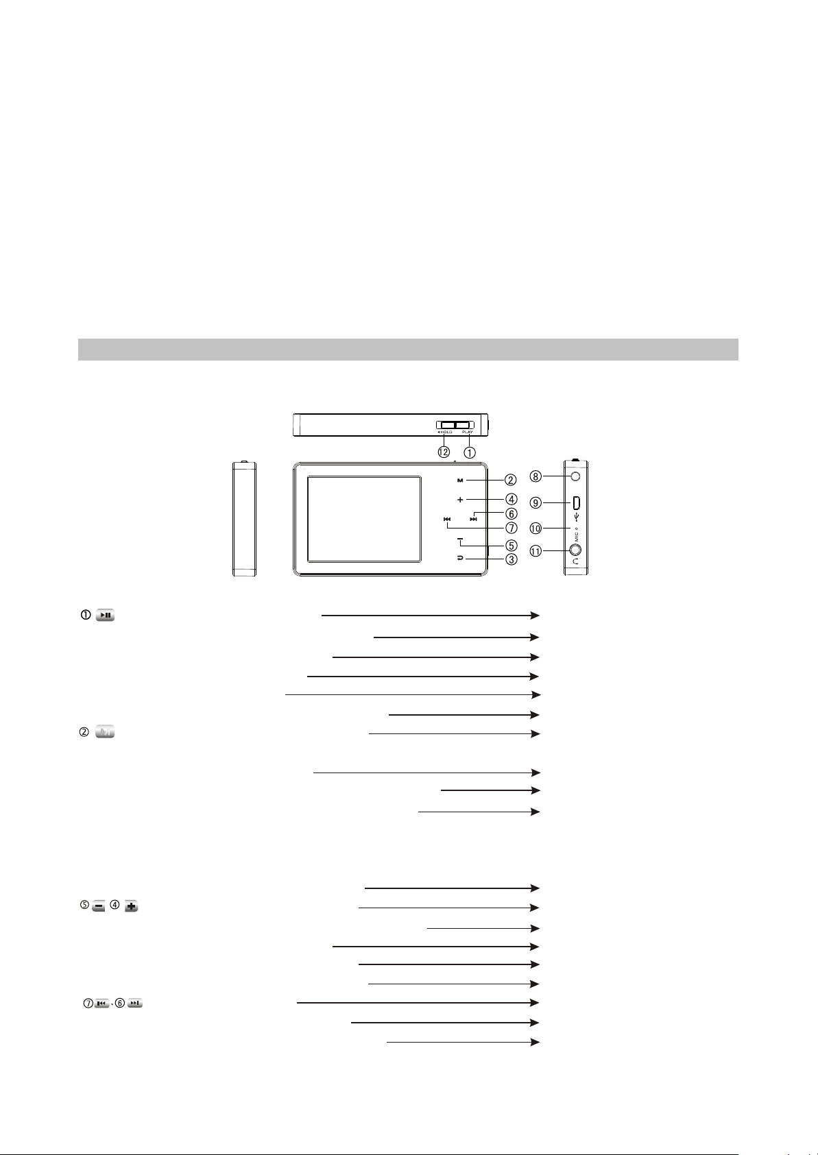
2.1.1 BUTTONS AND JACKS ILLUSTRATION
V3 video:
:
M
:
Push in power-off state
#
Push for long in power-on state
#
Push in playing interface
#
Push when recording
#
Push when tuning
#
Push when timing with stopwatch
#
Press when in menu operation
#
Press when recording
#
Press when in stopwatch timing interface
#
Press when in music playing interface
#
Press when in music playing, tuning, e-
#
book browsing, picture browsing and
recording preparation interface
:
Press when playing or tuning
#
Press when in "My sound effect setting"
#
Press when setting clock
#
#Press when browsing e-book
Press when in menu operation
#
:
#Press when playing
#Press for long when playing
#Press when in tuning preset state
power on
power off
pause/play switch
pause recording
mute
record time
enter the item or confirm the
setting
save record files
Time/pause timing
Exit and enter into main
menu interface
On-line menu pops up
adjust volume
Adjust dB value
set time
turn lines
Move cursor
the previous/next track
fast backward/forward
Select channel
- 4 -
Page 10
Press when in tuning search state
#
Press for long when in tuning search state
#
Press when in "My sound effect setting"
#
auto search
Automanual search
select the frequency that
you want to set
Press when browsing picture
#
#Press when browsing e-book
Press when in menu operation
#
:
#Press for long when in music playing
interface
switch pictures
turn pages
move cursor
A-B repeat
#Press for long when in file browsing
interface
#Press when in file browsing interface
Delete file
return to the previous
directory
#Press when in menu operation
not save the setting and then
exit from menu
Hanging rope hole
USB jack
MIC: microphone
Headphone jack
HOLD button: lock buttons when pushing towards arrow direction and unlock when
push towards the opposite direction.
2.1.2 POWER ON/OFF
#Power on
Press button to power on, the
power-on motion picture displays and
PUSH
system enters main menu.
NOTE:
If functions of playing, tuning or recording are not used during a specified period, this player will
power off automatically.
#Power off
PUSH
FOR LONG
Push button for long to power
off.
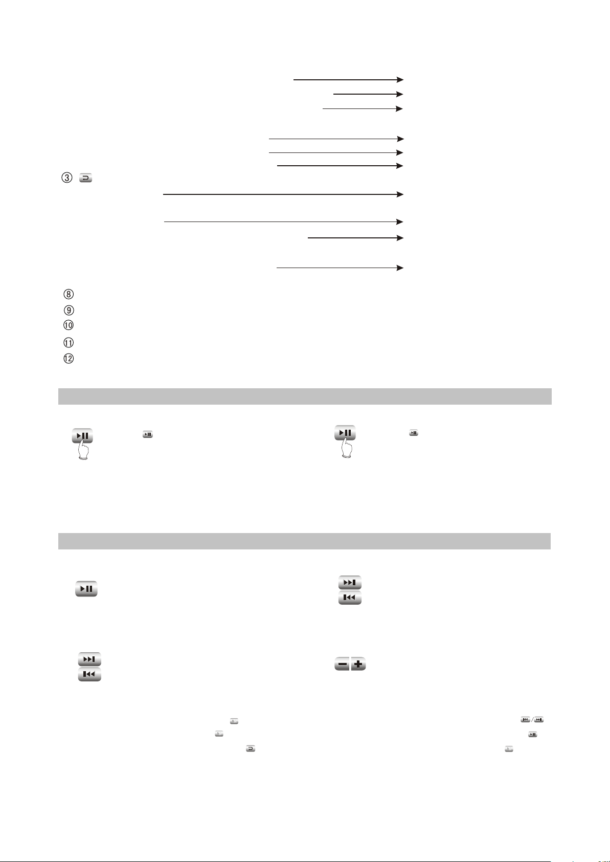
2.1.3 PLAY MUSIC
#Play/Pause
When playing music, pushing this
button may switch
between "Play" and "Pause".
#FF and FB
When playing music, press this
button for long and you may enter
fast forward or backward playback.
#NEXT and PREV
When playing music, press this
button to skip to the previous or
next track.
# Adjust volume
When playing music, press this
button or for long and you may
adjust volume.
#Play music
In "Music playing" menu, press button to enter Interface of browsing musical files. Press
button to select songs and press button to begin playing this song. When playing music, pushing
button may pause music playing, press button to return to the previous directory and press button
M
M
M
to exit and enter main menu interface.
- 5 -
Page 11
After pressing button to exit from on-line
menu, pictures will be played in the means of
M
PRESS
slide.
2.1.6 E-BOOK BROWSING
CAUTION:
#When the length of song's full path name is too
long, this song may probably not be played.
#When playing music, use picture browsing
functions and music will
stop playing.
2.1.4 VIDEO
In main interface, select "Video" item and
press button to enter.
After selecting movie files through pressing
button, press button to play movie and push
button to pause. When playing, pressing
button may skip to the previous or next movie,
pressing button to enter fast
forward/backward; pressing button to
adjust volume and pressing button may
return to the previous directory.
M
M
M
PRESS
After entering "E-book" item, press
button to select text file and press button to
browse e-book. Pressing button may
turn pages; pressing button may turn lines
and pressing button may enter on-line menu.
When browsing e-book, press button to
return to the previous directory.
M
PRESS
NOTE:
If some e-book format is not supportable,
please switch to TXT file with ANSI encoding
format
#Switch of ANSI encoding format
1. Select "Save" in
"File" item.
2. After dialogue box
pops up, select "ANSI"
in the pop-up options of
encoding and then click
"Save".
NOTE:
As for movie files with large capacity, you
need wait for several seconds to enter playing
after pressing button.
M
2.1.5 PICTURE BROWSING
After selecting picture file, press button to
M
enter picture browsing, press button to
switch pictures and press button to return to
the previous directory.
M
PRESS
When browsing picture, press button to
enter "On-line menu". In on-line menu, you may
set slide, rotate leftwards, rotate rightwards and
rotate 180 . Press button to enter "Slide";
after pressing button to select your desired
slide interval time, press button to confirm.
2.1.7 RECORDING
In main menu, select "Record" item and
press button to enter recording preparation
stage. Press button to enter recording/
pause recording. When recording, pressing
button may generate recording files and exit to
recording preparation state. Press button
to save recording files and exit to main menu.
Recording files are saved in "RECORDER" file
folder of "Music Playing" menu.
M
M
M
PRESS
- 6 -
Page 12
CAUTION:
#In order to avoid sudden power-off in the
course of recording, you cannot record when
battery is low and when disc is fully written; if
recording is in process, it indicates “FULL DISC”
and exits from recording.
#When recording with microphone, if you press
buttons and the sound of pressing may probably
be recorded.
2.1.8 TUNING
M
PRESS
In main menu, select "Radio set" item and
press button to enter tuning mode. Now,
M
insert headphone and you may listen to radio
program. After entering tuning mode,
pressing button may enter "On-line menu".
M
Press button to exit from tuning interface
and enter main menu, but tuning still
proceeds.
2.1.9 RESUME PLAYING
In main menu, after selecting "Resume
playing" item, press button to enter. In this
menu, you may select "Music resume", "Movie
resume" and "E-book resume". For instance,
select "Music resume" option, after
pressing button, this song begins playing
M
from the position where playing stopped last
time.
M
This player adopts lithium-ion battery to
supply power. In any case, connect MP4 player
to computer with USB line, it will power on and
begin to charge automatically. After fully charged,
the player will stop charging automatically.
CAUTION:
When charging, the player body is slightly hot,
#
and this belongs to normal phenomenon, so
please take it easy to use it.
#
When electric charge of battery is too low, and
when USB power supply is less than 100mA, it
begins to charge, screen may probably have no
display, and even battery charge is unavailable.
#It takes 3 hours to charge battery with computer .
#Before unplugging USB line, please stop using
USB memory function firstly. Data may be lost or
the player may be damaged if you unplug it
directly.
2.1.12 RESET
When this player cannot be operated, please
reset it.
Method for reset:
Push button for about 10 seconds. After
reset finishes, power on again and you may use
it normally.
2.2 USAGE INTRODUCTION
2.2.1 MAIN MENU ILLUSTRATION
M
PRESS
2.1.10 CALENDAR
In "Calendar" menu, you may set "Clock",
"Calendar" and Stopwatch".
M
PRESS
2.1.11 CHARGE
#Play music
Save audio files.
#Browse picture
Save picture files.
#Record
Select “Record” to enter
recording mode.
#Calendar
Select "Calendar"
item to enter this mode.
#Resume playing
Play from the position where
the music, movie and e-book
stopped last time.
- 7 -
Page 13
#Video
Save video files.
#E-book
Save text files.
#FM Radio
Select to enter radio
mode.
#Setup
Select "Setup" item
to set system options.
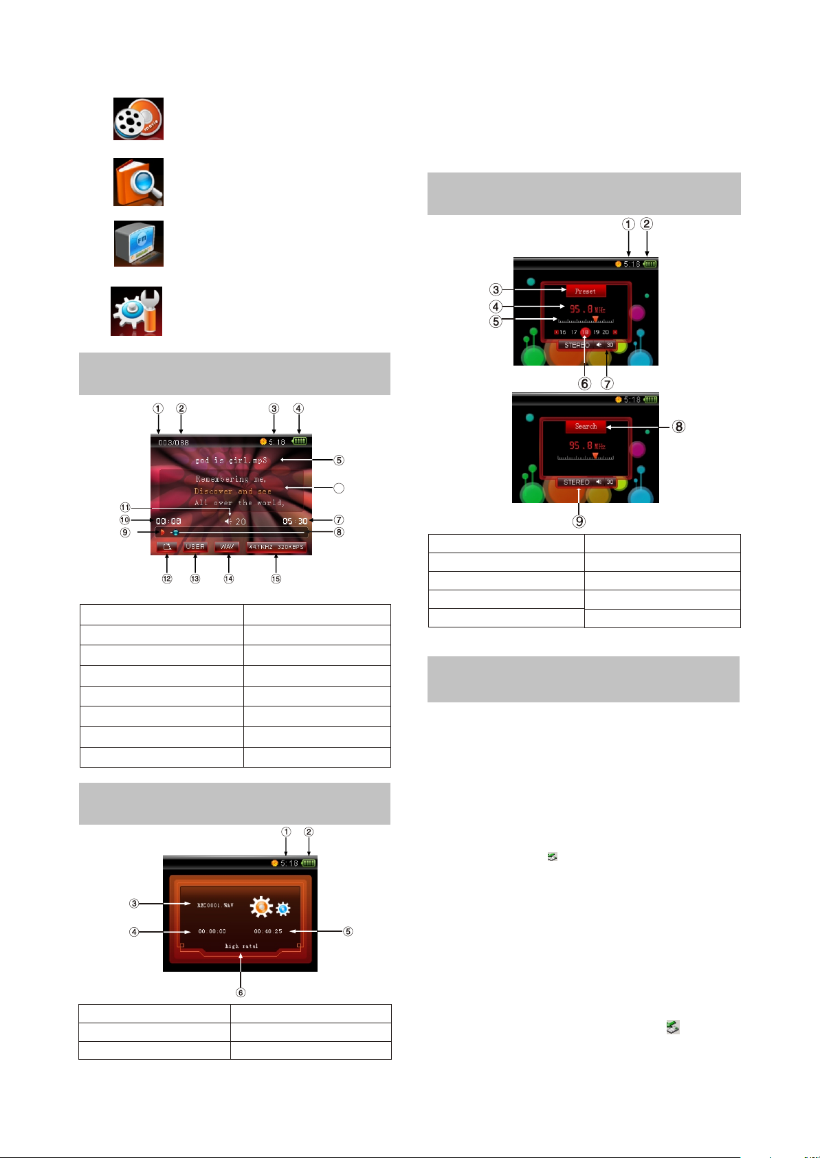
2.2.2 PLAYING INTERFACE
ILLUSTRATION
As for the name of recorded file “REC0001.wav”:
0001 is serial number of the current recorded
track and arranged according to sequence; WAV
is the file format after recording.
2.2.4 TUNING INTERFACE
ILLUSTRATION
6
1. Current track serial number
2. total track number
3.Clock
4. Battery capacity
5. Song name
6. Song name/singer/lyrics display
7. Total track time
8. Playback progress bar
9. Playback state
10. Current playback time
11. Volume
12. Playback mode
13. EQ mode
14. Music file format
15. Sampling rate\Bit rate
2.2.3 RECORDING INTERFACE
ILLUSTRATION
1.Clock
2. Battery capacity
3. Name of recorded file
4. Time that has been recorded
5. The left recordable time
6. Recording quality
1.Clock
2. Battery capacity
3. Preset mode
4. Frequency of the current radio station
5. Scanning progress bar
6. Radio station serial number
7. Volume
8. Scanning mode
9.Mono channel
2.3 BASIC OPERATION
2.3.1 USE MOBILE STORAGE
FUNCTION
This player may be used as mobile storage
in Windows ME/2000/XP operating system.
Under Windows 98SE operating system, the
player may be used as mobile storage after drive
program is being installed (please download it
from BBK official website).
Connect MP3 player and computer with USB
transmission line. After the bottom right corner of
desktop appears “ ”symbol, the mobile
storage function of MP3 player may be used
normally.
NOTES:
#To avoid abnormality of the player appears,
you are suggested to power off firstly before
connecting MP4 player with computer, and then
use USB transmission line to connect Mp4
player, then connect computer.
#In Windows 98 system, there is no “ ”
symbol.
- 8 -
Page 14
2.3.2 DISCONNECT USB SAFELY
After operation finishes, click “ ” symbol
on bottom right corner of Windows desktop with
right button of mouse, and disconnect USB
safely according to the computer prompt.
#Cancel file
When browsing files, press button for
long and the cancel dialogue box will pop up.
Press button to select "YES" and then
press button to cancel the file.
M
PRESS
FOR LONG
2.3.3 VIDEO CONVERSION TOOL
1. Brief introduction
before use, please download video conversion
tool and installation program “BBK MINIMP4
conversion tool” from BBK website and then
install to computer.
2. Basic operation
1) After program runs, click “Add conversion file”
button on the bottom left corner and a dialogue
box pops up, shown in the following figure:
2) According to the position indicated by finger,
click to select the source file required to
converse and the saving target path of new file
after conversing. Click "Save" button to add this
conversion into
conversion list. Multiple conversion tasks may
be added.
NOTE:
When in playing state, files cannot be cancelled.
2.3.5 PLAY MUSIC
#PLAY MUSIC
In “music”, press button to select song,
/
press button to begin playing music, and the
playback interface displays at the same time.
#Pause music
When playing music, press button to
switch to pause playing state, and press
button again to continue playing.
PUSH
#NEXT and PREV
When playing, pressing button may skip
to the next track to play; and pressing
button may skip to the previous track to play.
# FF and FB
When playing, pressing button for long
without loose may realize fast forward.
3) Click "Begin to converse file" button to start
conversing, shown in the above figure:
2.3.4 BROWSE/CANCEL FILE
#Browse file
In main menu, audio files are saved in
"Music playing" item.
Press or button to select files to
browse upwards or downwards.
PRESS
PRESS
FOR LONG
When playing, pressing button for long
without loose may realize fast backward.
#ADJUST VOLUME
When in playback interface or listening to
radio set, pressing button or for long may
both adjust volume.
NOTE:
#In some operating system (such as complex
font Windows), the operation of copying
lyrics/song file and changing song's name may
- 9 -
Page 15
Probably lead to incorrect display. When playing
non-standard songs or songs with special format,
noise may probably occur.
2.3.6 A-B REPEAT FUNCTION
When playing, if you want to listen to content
of a certain segment repeatedly, please use A-B
repeat function. Press button for long for the
first time to select the beginning point that you
want to play repeatedly and screen displays“A”;
press button for long for the second time to
select the end point that you want to play
repeatedly and screen displays “A-B”and system
begins to repeat during“A-B”period; press
button for long for the third time to cancel A-B
repeat and playing continues.
PRESS
FOR LONG
PRESS
FOR LONG
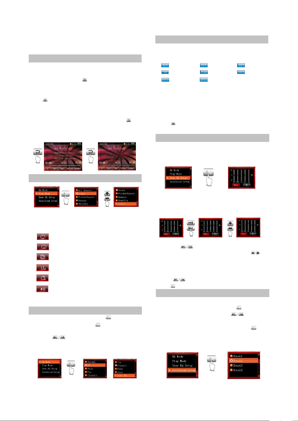
2.3.7 PLAYING MODE
2.3.9 EQ MODE
The corresponding icons of each EQ mode
in playback interface are shown as follows:
NORMAL
3D
ROCK
POP
CLASSIC
DBASS
JAZZ
MY EQ
Select “MY EQ”, and correspond with the
sound effect that you have preset in “On-line
menu” in playback mode. If you have not set “MY
EQ”, it is defaulted “NORMAL” sound effect,
When cursor moves to a certain sound effect,
press button to confirm the selection of this
EQ mode.
2.3.10 MY EQ SETUP
In "My EQ setup" interface, the range value
(dB) of each frequency range may be increased
or decreased.
M
PRESS
M
PRESS
PRESS
The playback mode icons displayed on playback
interface are shown as follows:
: Repeat playing all tracks.
: Play according to track sequence.
: Repeat file folder.
: Repeat playing single track.
: Play any track at random.
: Browse play each track for 10
seconds.
2.3.8 EQ MODE
When playing music, press button to
enter “On-line” menu, press button to enter
“EQ Select”, and then move cursor through
pressing button to select proper EQ
mode.
M
M
If you want to adjust the range of mediant (1K),
you may operate according to the following
diagram:
PRESS
PRESS
Press button to select the frequency
range that you want to adjust, and press
button to adjust the range value. When adjusting
the range, take 2dB as a step, and the max
adjustable scope is 6dB. After setup finishes,
++
--
press button to confirm and exit;
press button not to save and then exit.
M
2.3.11 WALLPAPER SELECT
When playing music, you may select
wallpaper in“On-line” menu. Press button to
enter “On-line”menu and press button
to move cursor to "Wallpaper select" item. Select
your favourite wallpaper and then press
button to confirm.
M
M
M
PRESS
M
PRESS
- 10 -
Page 16
2.3.12 RECORD
In main menu, after selecting “REC”, press
button to enter recording ready state. In
recording ready state, press button to pop up
M
on-line menu.
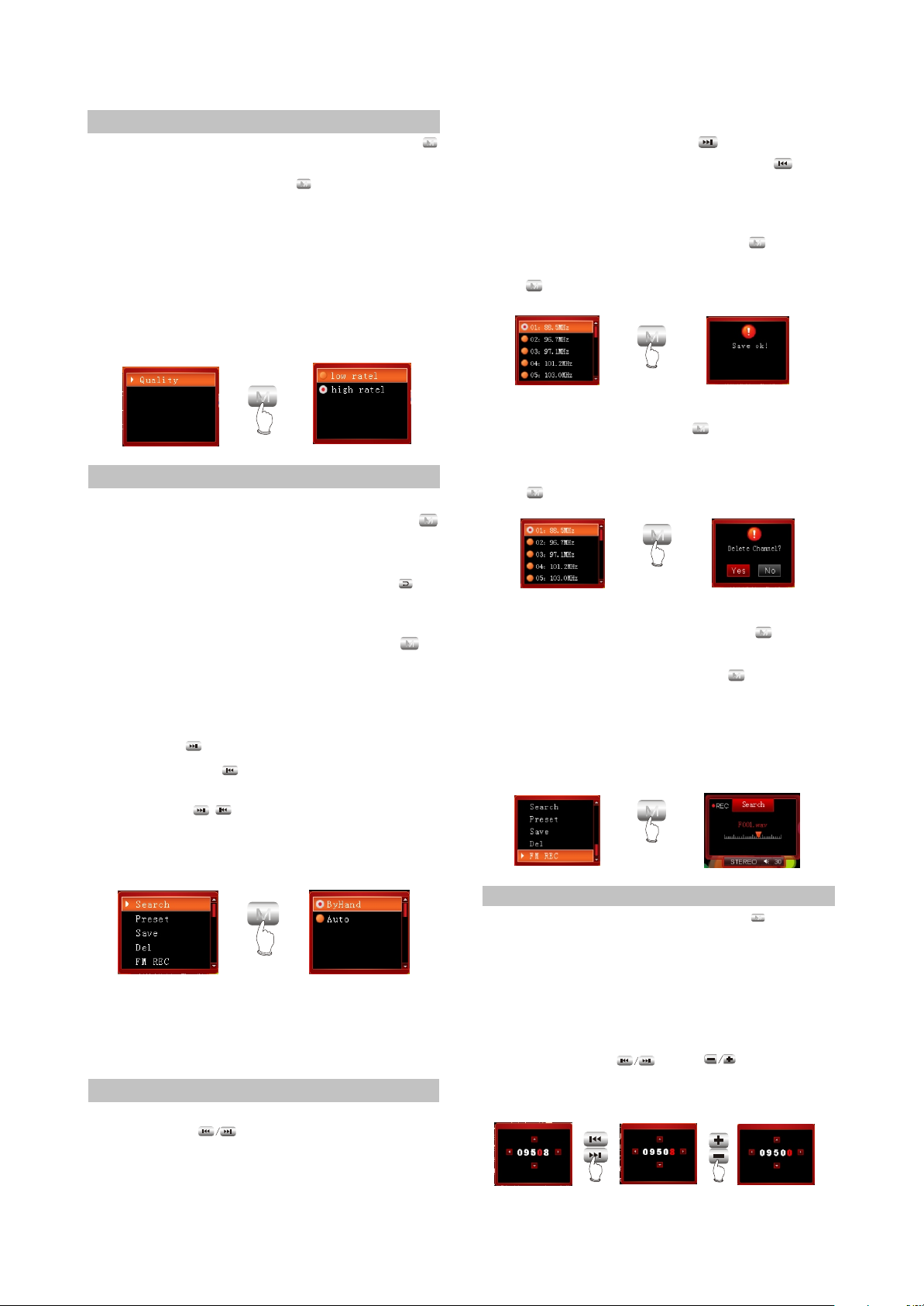
# Recording quality
If recording quality is higher, sound quality is
better and space occupied is more. The two
kinds of recording quality both adopt ADPCM
format encoding, which is only effective to MIC
recording.
M
#Preset
In preset mode, pressing button may
adjust to the next channel and pressing
button may adjust to the previous channel.
#Save
In manual or automanual scanning mode,
after radio station is searched, press button
M
to enter on-line menu. After selecting "Save",
press button to confirm.
M
M
PRESS
M
PRESS
2.3.13 TUNING
#Enter radio set mode
Select "Radio set" in main menu and press
button to listen to radio program.
#Quit radio set mode
When listening to radio program, press
button to exit and enter main menu.
#Search
When listening to radio program, press
button to enter on-line menu.
There are two kinds of scanning mode of
“Manual” and “Auto”.
1. Manual scanning
Pressing button may add 0.1MHZ each
time and pressing button may decrease
0.1MHz each time.
Pressing / button for long may
increase or decrease frequency continuously
and will stop until radio station is searched.
#Delete
In tuning interface, press button to enter
M
on-lin menu, select “Delete” item, move cursor to
the frequency point that you want to delete and
press button to confirm.
M
M
M
PRESS
#FM recording
M
When listening to radio set, press button
to pop up “On-line” menu and select “Record”
item to enter FM recording. Press button to
M
M
generate recording file and exit to tuning state.
Format of file generated from FM recording is
WAV format and this file is saved in“FM REC” file
folder of “Music playing”.
M
PRESS
M
PRESS
2. Auto scanning
In on-line menu, after selecting "Auto" item,
full auto scanning starts and all radio stations
searched will be saved automatically.
NOTE:
During the course of (full-auto/automanual)
scanning, pres button and scanning will be
stopped.
2.3.14 E-BOOK
When browsing e-book, pressing button
may enter "On-line" menu.
In on-line menu, you may set jump pages, save
bookmark, extract bookmark, delete bookmark,
auto page down, music playing, style select and
font size.
#Jump pages
You may press and button to
set page by using this function, shown in the
figure:
- 11 -
M
Page 17
After setup finishes, press button to confirm.
M
#Save bookmark
In on-line menu, select “Save bookmark” item
and press button to enter. Pressing button
M
M
may select th position to save and pressing
button may set the current page as bookmark.
M
PRESS
#Extract bookmark
In on-line menu, select Extract book
mark" item and press button to enter.
M
Press button to select your desired
bookmark and then press button to confirm.
M
#Delete bookmark
After selecting "Delete bookmark" item,
press button to make dialogue box pop up.
Select "OK" item and then press button to
M
M
delete bookmark.
#Auto page down
After pressing button to enter on-line
menu, select "Auto page down" item and press
M
M
button to enter interval time setup of page down.
After selecting your desired interval time,
press button and the E-book will turn pages
M
Automatically.
#Music playing
After setting "Music playing" item in "ON",
you may browse E-book while listening to music.
#Style select
In "Style display" item, you may set your
favourite style according to your own likes.
2.3.15 CALENDAR
#Clock
In "Calendar" menu, press button to enter
"Clock" item and you may set the current time.
Press button to select time format: 12hour or 24-hour system.
PRESS
Use and button to set the
current time and then press button to
confirm.
M
M
#Calendar
M
Press button to enter "Calendar" setup.
Use and button to set date.
#Stopwatch
In "Stopwatch" menu, press button to start
M
Timing. When timing,
Push button to save record and press
M
button to stop timing
M
PRESS
2.4 SYSTEM SETUP
2.4.1 LANGUAGE
#Language
Press button to enter the setup, press
button to select language and press button to
confirm. After setup is ok, press button to
return to the previous content.
2.4.2 TIMING POWER-OFF
#Timing power-off
Press button to adjust timing power-off
time. After setup is ok, press button to confirm.
If the timing power-ff time is set in 15-min, after
15 minutes this player will power off
automatically.
CAUTION:
#Invalid is defaulted each time when power on.
#Timing power-off time is rough time and it may
probably have deviation.
#When recording, please do not set timing
power-ff, otherwise the recording files cannot be
played normally.
2.4.3
#Screen saver time
After pressing button to select screen
saver time, press button to confirm. If screen
saver time is set in 15 seconds and no operation
happens within 15 seconds, this player will enter
screen saver state automatically.
M
M
M
SCREEN SAVER TIME
M
- 12 -
Page 18
CAUTION:
#Screen saver time is rough time and it may
have difference when playing songs with
different formats.
#Screen saver function is not available when in
video playing, stopwatch, Ebook and pictures.
2.4.4 BRIGHTNESS
#Brightness
Press button to select proper
brightness and then press button to confirm.
M
2.4.5 FM CHANNEL
# FM Channel
You can select the FM channel in settings.
When select Auto, it changes the channel
Automatically. When select Mono, it tunes
atMono channel all the time.
CAUTION:
“General radio station" is the default value
each time when power on.
2.4.6 SOUND OF PRESSING
BUTTON
#Sound of pressing button
After entering this menu, you may set "On" or
"Off" for the sound of pressing buttons. When
dialogue box pops up, press button to
move cursor to "On" and then press button to
confirm.
M
2.4.7 DEFAULT SETTINGS
#Default settings
If you want to restore this player in factory
settings state (material and song file will not be
deleted), you may select "Default settings".
Press button to enter this menu, after
dialogue box pops up, select "Yes" and then
press button to restore in "Default settings".
2.4.8 FIRMWARE UPGRADING
# Firmware upgrading
This player supports firmware upgrading.
Please refer to the description on BBK website
for details.
CAUTION:
After upgrading, disk will be formatted, so
please pay attention to backup materials before
upgrading.
2.4.9 SYSTEM INFORMATION
#System information
In this item, you may check information of
memory, remained memory and version number.
CAUTION:
Because firmware will use some space, the
displayed content capacity may probably be
different from the actual capacity.
2.4.10 FORMAT
#Format
When using computer to format this player,
please select FAT32 file system, otherwise this
player will work abnormally.
2.5 SPECIFICATION
Model
Audio decode chip
Lithium battery
Continuous playback time
Size/weight
Audio SNR
Headphone output
Frequency range
FM tuning range
Working temperature
Audio file
Picture file
V3 video
WOLFSON WM 8750
3.7V 650mAh
Longest continuous playing
time for MP3 is 11 hours
Size: 85.5mm 50mm 10mm
weight: 66.2g
90dB
12mW+12mW 32 ohm (25mW+25mW when headphone impedance is 16-ohm)
18Hz~20kHz
76MHz~108MHz
0 C~35 C
MPEG 1/2 Layer 3(32kbps~320kbps),
WMA(32kbps 320kbps), WAV
Support DCF standard JPEG format,
6~8 million pixel at most is supportable, BMP
V5 video
WOLFSON WM 8750
3.7V 900mAh
Longest continuous playing
time for MP3 is 15 hours
Size: 87mm 54mm 11mm
weight: 76g
#Design and specifications of product are
subject to change without notice.
- 13 -
Page 19
Chapter Three Principle and Servicing
Section One Principle of the Player
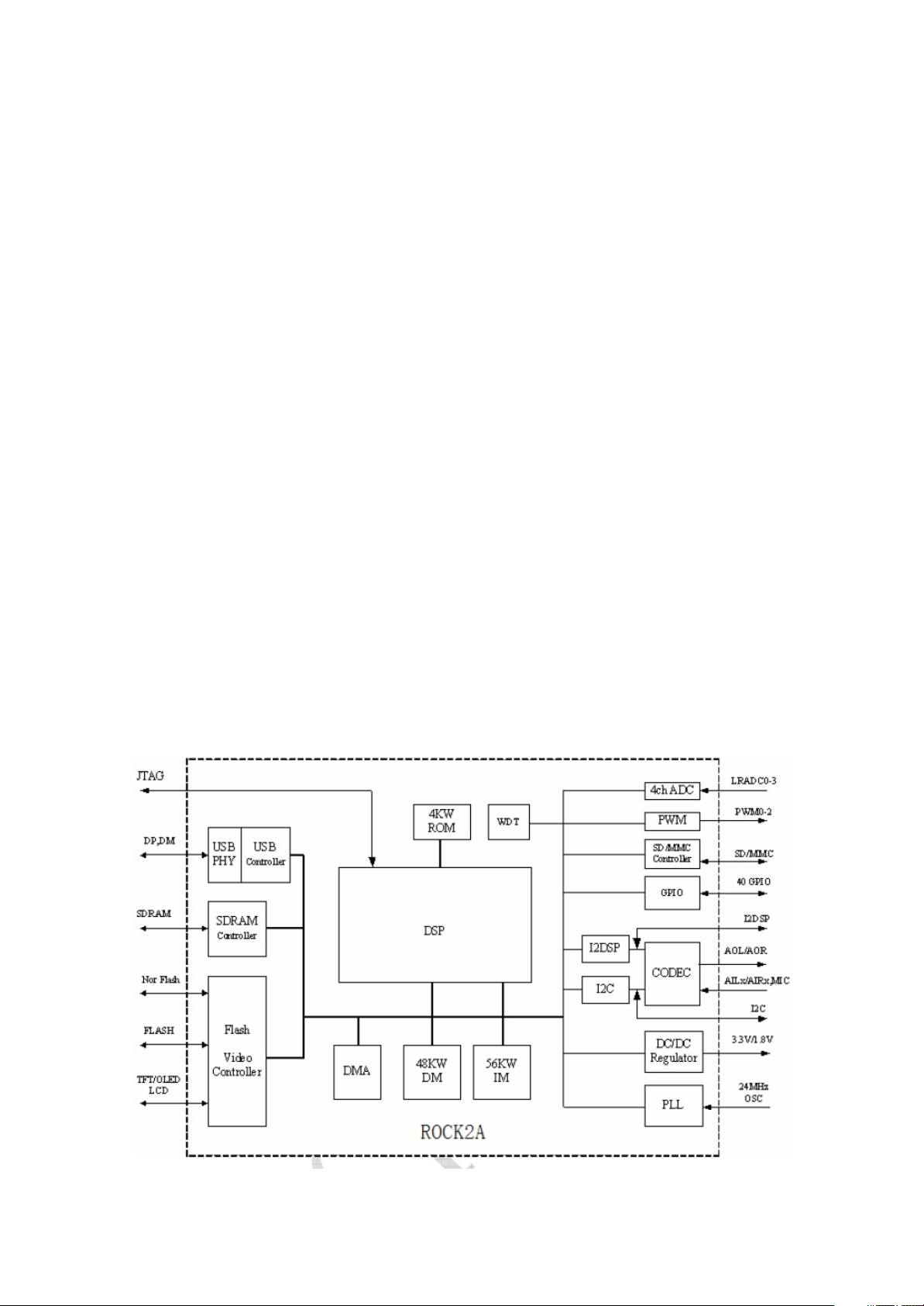
3.1.1 Block diagram of the player
Block diagram of the player is shown in the picture 3.1.1.1:
POWER
MANAGEMENT
MODULE
POWER
ADAPTOR
CHARGE
MANAGEMENT
SDRAM
LDO CIRCUIT
TPS79333
DC-DC CIRCUIT
TPS62200
USB INTERFACE
AUDIO&VEDIO CODEC
USB POWER
24M CRYSTAL
LI-ION BETTERY
HEADPHONE
MICROPHONE
AUDIO CODEC
WM8750
RK2608
FLASH MEMORY
FM MODULE
TEA5767
QVGA LCD
LDO BACKLIGHT
RT9284
SWITCH CIRCUIT
RESET CIRCUIT
TOUCH-BUTTON
CONTROL
CY8C21434
TOUCH-BUTTON
ARRAY
Figure 3.1.2.1 Block diagram of the player
3.1.2 Principle of the player
V3/V5 portable Mp4 player is mainly composed of the following functional modules:
1. Decode part: main video decode chip adopts Rk2608 decode chip of Rockchip Company with
built-in ROM and RAM, which may directly drive TFT LCD screen. Main audio decode chip adopts
Wm8750 decode chip of Wolfson Company.
- 14 -
Page 20
2. Power supply part: composed of lithium battery, TPS79333, TPS62200 and XC6206, which is
Location number Chip Function
U1 HY57V641620ETP-7 SDRAM
U2 RK2608 Main video decode board
U3 RT9284B 12V voltage DC-DC conversion
U4, U5 K9G8G08U0M FLASH
U6 TPS62200 1.8V voltage DC-DC conversion
U8 MCP73832 Charge management
U9 TEA5767HN Tuning chip
U10 M41T62 Real-time clock
U11 WM8750BL Audio encode/decode
U14 XC6206P152MR 1.8V voltage stabilizing
U15 CY8C21534 Touch button control
U16 TPS79333DBVR 3.3V voltage DC-DC conversion
Location number Chip Function
U1 WM8750BL Audio encode/decode
U2 HY57V641620ETP-7 SDRAM
U3 RK2608 Main video decode
U4, U5 K9G8G08U0M FLASH
U6 M41T62 Real-time clock
U7 TEA5767HN Tuning chip
responsible for power supply circuit of each part of the entire MP3.
3. Peripheral jack” composed of headphone output port, MIC input port and USB jack. Headphone
jack is the audio output jack of the player, MIC is the audio input jack of external recording and USB jack
fulfills internal and external data exchange of the machine to realize charge function.
4. Data storage module: composed of Flash and peripheral circuit to fulfill data storage of the player.
5. Display module: V3 adopts 2.4” high-bright QVGA screen and V5 adopts 3” high-bright 16:9 LCD
screen.
6. Tuning module: FM tuning.
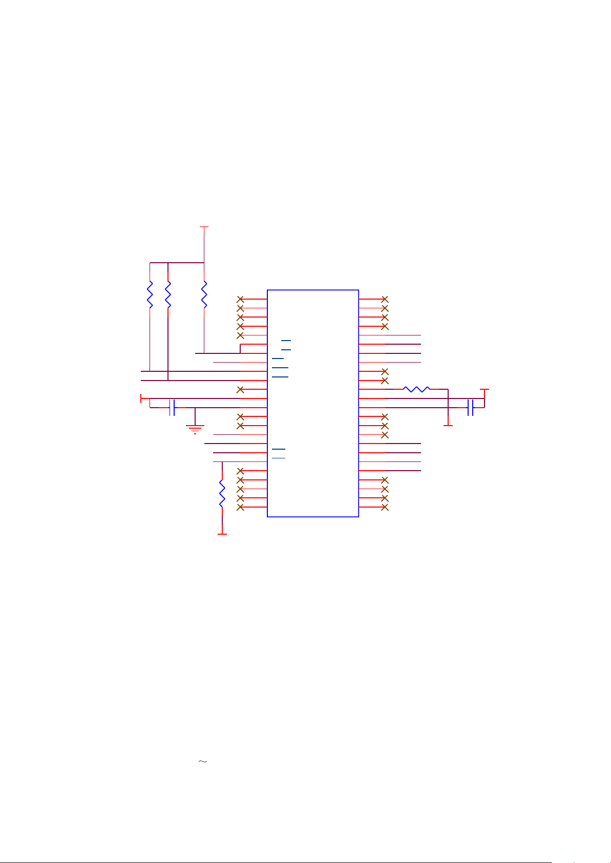
3.1.3 Introduction to IC used by the player
1. IC used by the main board of V3 is shown in the following picture:
2. IC used by the main board of V5 is shown in the following picture:
- 15 -
Page 21

U8 SSD1928QL9 LCD drive
U10 RT9284B 12V voltage DC-DC conversion
U11 TPS79333DBVR 3.3V voltage DC-DC conversion
U12 TPS62200 1.8V voltage DC-DC conversion
U13 MCP73832 Charge management
U14 XC6206P152MR 1.8V voltage stabilizing
U15 CSTCR4M00G55 SMD ceramic resonance
U1 CY8C21534 Touch button control
- 16 -
Page 22
Section Two Unit Circuit Principle
3.2.1 Video decode circuit principle
1. Video decode circuit is mainly composed of main decode chip Rk2608, SDRAM and peripheral
circuit. Rk2608 may realize video file decode playing of MPEG-4 format in low frequency and power
consumption with clear and smooth picture quality, meanwhile, Rk2608 integrates large amount of I/O
control jacks which may provide the max flexibility. The internal principle block diagram of Rk2608 is
shown in the picture 3.2.1.1. Low power consumption function of Rk2608 may prolong battery usage
time for portable player and its integrated intelligent lithium battery charger supports voltage control
(AVC) and its integrated power management unit includes a DC-DC converter on high effective plate,
which supports multiple battery configuration, such as 1×AA, 1×AAA and Li-ion battery. What’s more,
compared with the traditional voltage control system, AVC enables chip to operate with higher peak
value CPU working frequency to make the highest running speed up to 100 MIPS. Rk2608 supports
DRM10 digital copyright management technology based on SOFTWARE. Rk2608 with multi-function
management function, which may realize the function that listening to music while viewing e-book or
playing e-games. Rk2608 chip integrates USB 2.0 High Speed/Full Speed PHY with hugher
transmission speed and integrates the controller that supports TFT/CSTN/OLED colorful screen.
Figure 3.2.1.1 Internal principle block diagram of Rk2608
- 17 -
Page 23
2. Working principle: when the machine power on, reset circuit keeps high level reset signal. After
RK2608 completes reset through reset pin 113, reset signals output from pin 56 to pin 42 of SSD1928 to
enable SSD1928 to finish reset (V3 screen need no SSD1928 drive, so there is no this reset process), at
the same time reset signals are sent to enable end of RT9284, boost circuit begins to work and screen is
lightened. Meanwhile, 1.8V and 3.3V power circuit begins to supply power for RK2608, 24M crystal
oscillator Y1 oscillates and decode chip begins to work and read data saved in Flash. After RK2608
decoding, video signals are sent to SSD1928 to drive LCD screen to display through SSD1928.
3.2.2 Audio decode circuit principle
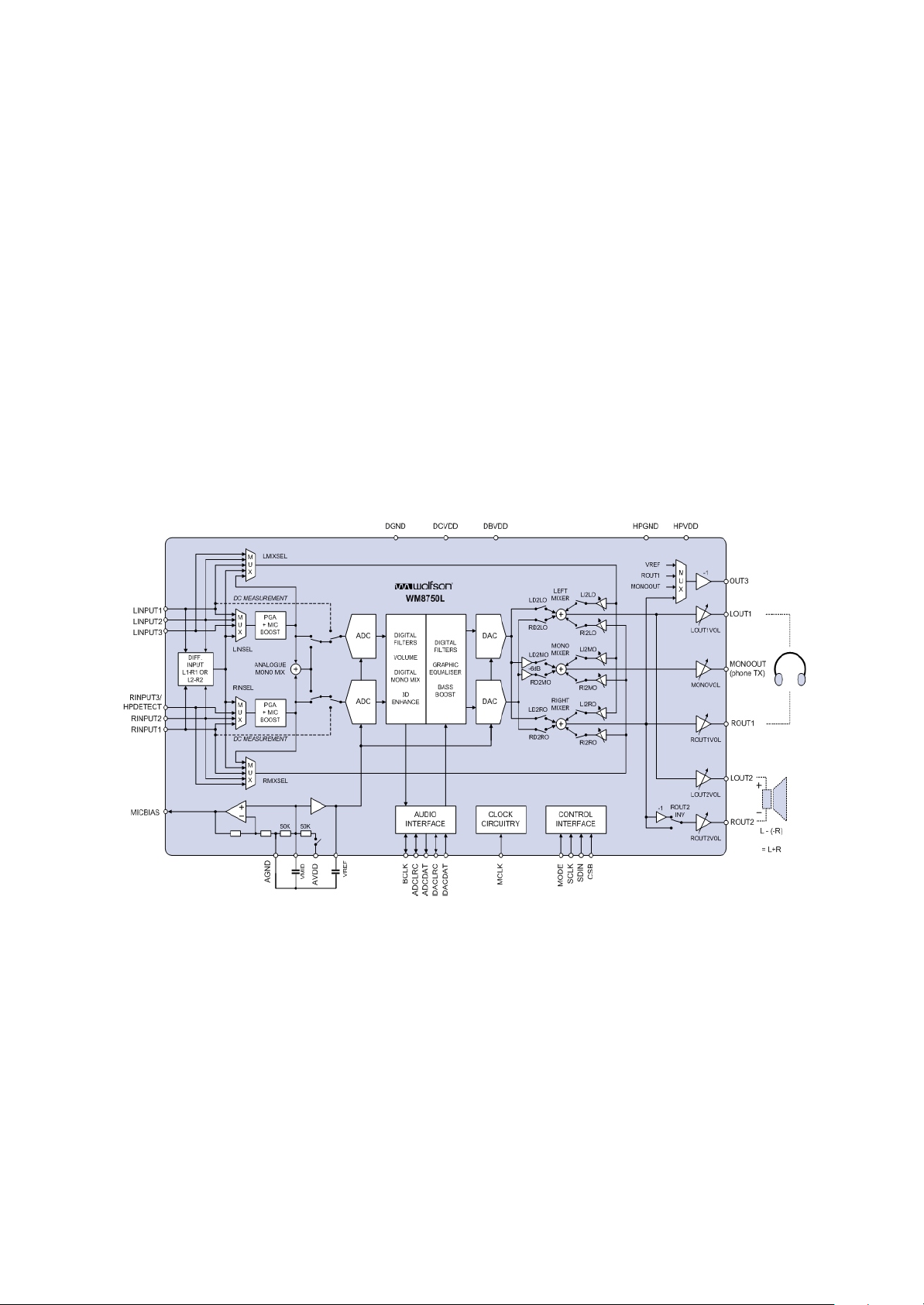
1. Audio decode circuit is mainly composed of decode chip WM8750 and peripheral circuit. WM8750
is a stereo coder/decoder with low power consumption and high quality, specially designed for portable
digital audio application. WM8750 adopts I2C bus mastering means and its internal principle block
diagram is shown in the picture 3.2.2.1.
Figure 3.2.2.1 WM8750 internal principle block diagram
2. Working principle: the digital audio signals that output after being decoded by the internal decode
circuit of RK2608 are sent to WM8750 inside for DA conversion through pin 6 of WM8750 and the analog
audio signals after conversion are sent to headphone jack for output through HP_OUTR and HP_OUTL.
When the machine is recording, external analog audio signals pass through microphone and an
INPUT pin (pin 24) of WM8750 and then are sent to AD conversion unit of WM8750 for AD conversion
and then for digital filtering, volume control and echo processing inside. The digital audio signals after
being processed are sent to main decode chip RK2608 for processing and then saved in Flash.
- 18 -
Page 24
When machine is in FM state, FM digital audio signals input from INPUT pin (pin 27, 28) of
WM8750, after digital filtering and echo processing inside WM8750, and then output to headphone jack
directly.
3.2.3 FLASH circuit
1. FLASH circuit schematic diagram is shown in the figure 3.2.3.1:
VCC
R35
47K
VCC
R36
47K
FCE0
FCE1
C39 104
GND
R37
10K
RD/BY
FREN
FCLE/A2
FALE/RS/A1
FWEN
FWP
R40
47K
D_GND
U4
1
RES#
2
NC
3
NC
4
NC
5
NC
6
R/B2
7
R/B1
8
RE
9
CE1
10
CE2
11
NC
12
VCC
13
VSS
14
NC
15
NC
16
CLE
17
ALE
18
WE
19
WP
20
NC
21
NC
22
NC
23
NC
24
NC
NAND FLASH
NC
NC
NC
NC
I/O7
I/O6
I/O5
I/O4
NC
NC
PRE
VCC
VSS
NC
NC
NC
I/O3
I/O2
I/O1
I/O0
NC
NC
NC
NC
48
47
46
45
44
43
42
41
40
39
R32 0R
38
37
36
35
34
33
32
31
30
29
28
27
26
25
D7
D6
D5
D4
D3
D2
D1
D0
VCC
C40
104
D_GND
Figure 3.2.3.1 Flash circuit schematic diagram
2. Working principle: Flash Memory is the storage unit of the player and all AV and image files must
be stored in FLASH. Flash module is composed of two groups of FLASH chip K9G8G08U0M with the
specification 2G (H model is 4G). Flash chip and main decode RK2608 are connected through 8 data
lines to complete the read, write and delete of inside files. VCC provides 3.3V voltage for FLASH
working. R35, R36 are pull-up resistor of /CE and R40 is pull-down resistor of /WP. VCC is power supply
pin of FLASH. /CE is chip-selection signal, effective when in high level. VCC supplies 3.3V voltage and
FLASH begins working. /RE, /WE are read-effective and write-ettective signal ports to control rear and
write function of FLASH. I/O1 I/O8 are 8 data lines to fulfill the exchange of FLASH and outside data to
realize the function of write, delete and edit of Mp3.
- 19 -
Page 25
There is firmware of the player’s working inside Flash and all tasks are completed by CPU to send
out relevant order after the data exchange between CPU and Flash. When the player power on, 3.3V
voltage supplies power for Flash through VCC, /CE inputs 3.3V high level signal and Flash begins to work
effectively. When playing video files, /RE is high level, Flash performs the operation of read out. When
files are written in through USB data line or recording through microphone, /WE is high level and Flash
performs the operation of writing in. The operation of read out and writing in is performed through
I/O1~I/O8 dateladdress lines.
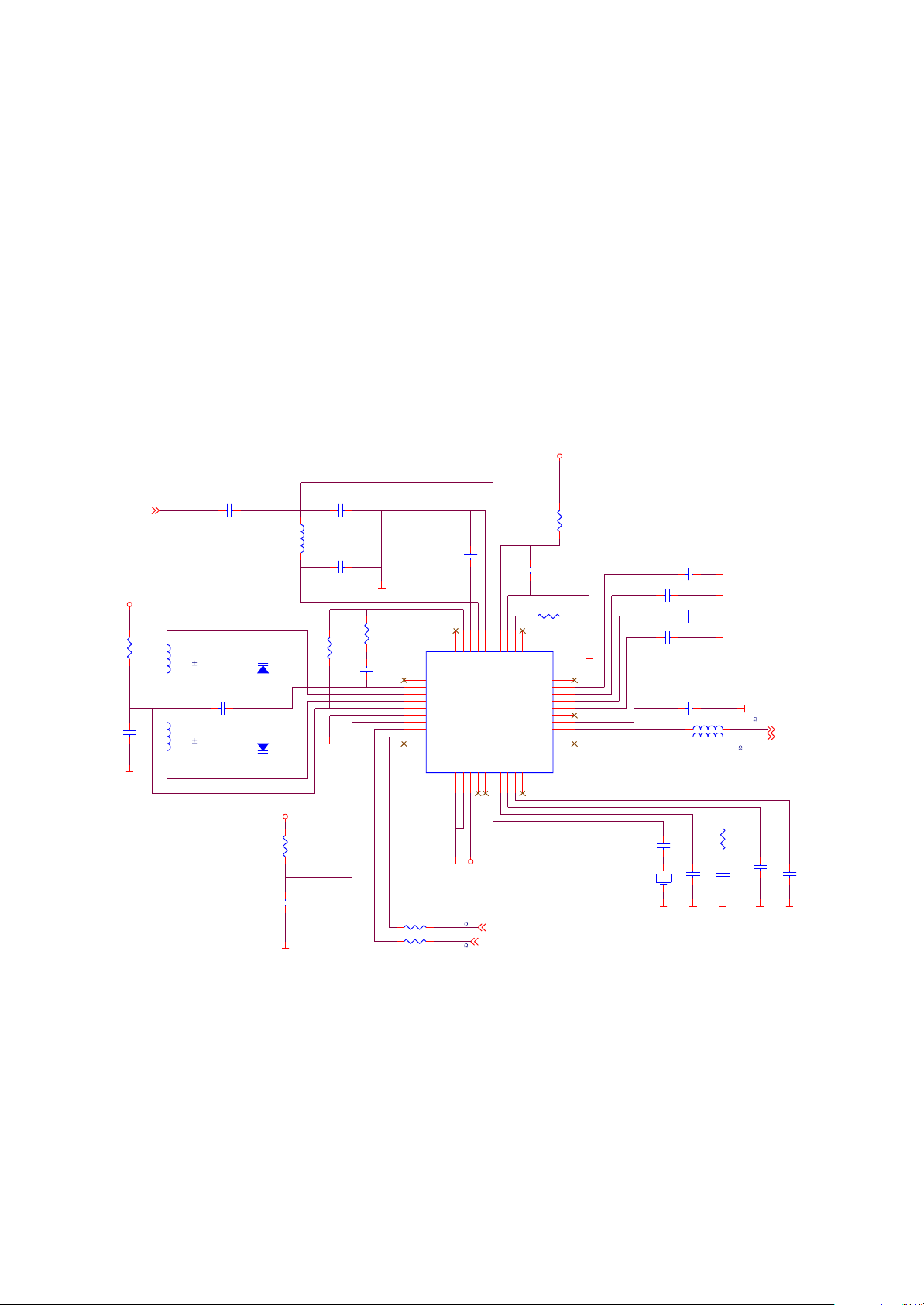
3.2.4 FM tuning circuit
1. FM tuning circuit diagram is shown in the figure 3.2.4.1
FM_3V3
R69
22R
C68
104
FM_ANT
FM_3V3
FSGND
FM_ANT
L17
33nH 2%
L18
33nH 2%
C66 103
C56 101
R73
22R
D10
BB202
D11
BB202
FM_3V3
FDGND
C76
104
L16
120nH
C57 27PF
FDGND
C59
47PF
R70
100K
FSGND
R68
10K
C65
393
L23 601 DCR<350m
L24
C58
472
1
N.C
2
CPOP
3
VCOT1
4
VCOT2
5
VCOVCC
6
DGND
7
DVCC
8
DATA
9
CLOCK
10
N.C
FDGND
601 DCR<350m
40
N.C
W/R11BUSM12BUSEN13SWP114SWP215XTAL116XTAL217PDLF18PHLF19N.C
36
37
38
39
RFI2
TCAGC
RFGND
LOOPSW
TEA5767HN
NECTAR-I
FM_3V3
I2C_SCL
I2C_SDA
33
34
35
RFI1
AVCC
32
AGND
R67 18K
31
N.C
IFGAI
DIFL2
DIFL1
TCIFC
VREF
MPXO
TMUTE
RAVO
LAVO
20
C60
475/X5R
N.C
N.C
R66
10R
C61 473
C63 473
C67 333
601 DCR<350m
L7
L8
601 DCR<350m
C73
22PF
FDGND
FSGND
FSGND
FSGND
FSGND
FDGND
FSGND
R72
33K
C74
223
FDGND FDGND
C72
223
5767R
5767L
C75
102
C62 473
XT1
32.768KHz
C64 333
C71
102
FDGND
U9
FSGND
30
29
28
27
26
25
24
23
22
21
Figure 3.2.4.1 FM tuning circuit diagram
2. Working principle: tuning circuit is composed of the micro digital tuning IC TEA5767 of Philips
Company and peripheral circuit. C56, C57, C58, C59, L16 is the antenna input matching circuit of FM
module; variant diode D10, D11 and winding inductor L17, L18 is frequency selection tuning circuit in FM
module. The control of FM adopts IIC bus control means and 9, 10 of TEA5767 are data and control
lines.
- 20 -
Page 26
When MP3 player switches in FM tuning state, antenna is sent to the RF band-pass filter
(87.6MHz~108MHz and 76MHz 87.5MHz) composed of Li6, C57 and C59 through C56 coupling and
then to pin 35, 37 of TEA5767 for amplifying through TEA5767 inside. Pin 2, 3, 4 of TEA5767 is
connected with the internal VCO and with variant diode D10, D11 externally. Pin 2 id tuning voltage
output pin and voltage changes within 1V when in auto search. VCO power supply is sent to pin 5 of
TEA5767 by FM 3V3 through 69 limit and C68 filtering. The built-in I2C jack is controlled through pin 8, 9
of TEA5767 and CPU performs operation of channel search and selection through I2C bus. Digital power
is sent to pin 7 of TEA5767 by FM 3V3 through R73 limit and C76 filtering. XT1 (32.768) produces basic
clock of 32.768 and inputs to TEA5767 from pin 17. Analog audio signals after being processed by
TEA5767 output to rear stage power amplifying circuit from 23 (right channel), 22 (left channel) for
amplifying and then output through headphone jack.
3.2.5 Display screen boost circuit
1. Display screen boost circuit diagram is shown in the picture 3.2.5.1:
VB
L9
601/0603
C35
106/X5R
BACK_EN
BACK_L
R61
0R*
R59 1K
R60
10K
L10
CDRH3D16-100
R63
0R*
Figure 3.2.5.1 Display screen boost circuit
6
VCC
4
EN
2
GND
U3
RT9284B
LX
OVP
FB
D3
MBR0520/SOD123
1
5
3
C5
102
R30
12R¡À1%
LED-
D_GND
L11
601/0603
C36
106/16V/1206
LEDP
LED+
2. Working principle: 12V high voltage is needed for lightening display screen, so the boost circuit
must be matched to fulfill. This circuit includes two parts: boost circuit and display screen jack circuit.
Boost circuit is composed of DC-DC control IC Rt9284 and peripheral circuit; VIN is power input; EN is
enable end of Rt9284, effective when in high level; SW is high voltage output pin and FB is feedback pin.
After power on, the internal boost circuit of L10 and Rt9284 begins to boost and storage energy.
When current of L10 reaches 750mA, RT9284 internal switch turns off, and supplies power for the rear
circuit through external diode D3 at the same time when the switch is off. Voltage divide detect circuit
sends the detected voltage in pin 3 of RT9284. When detect voltage of pin 3 is lower than 1.235V
reference voltage (this IC has a 1.235V reference voltage comparator inside), the internal switch is on,
the internal boost circuit of L10 and RT9284 begins to boost and store energy. When current of L10
- 21 -
Page 27

reaches 750mA, the internal switch of RT9284 turns off, and supplies power for the rear circuit through
external diode D3 at the same time when switch is off until feedback voltage is lower than reference
voltage again. As for this PFM peak current control scheme adopted by convertor and discontinuous
conduction means (DCM), the frequency depends on output current and makes the frequency of entire
load very high. Pin 4 of RT9284 is working enable pin and connected with pin 56 of RK2608 to control
level change through software and control RT9284 to realize screen-save function.
When machine power on, display screen perform data communication through rear CPU and
restores the drive current signals sent from CPU on display screen. Signals sent from CPU are different
and display screen makes different displays, so we may see different displays and CPU also controls
screen-save function through software setup.
3.2.6 USB jack circuit
1. USB jack circuit is shown in the picture 3.2.6.1.
D_GND
R3
J1
+5V
D-
NC
D+
GND
IN_L
IN_R
GND
3DU05S-32T-10
D_GND
SFI0402-050E100NP
C6
1
2
3
4
5
6
7
8
L6 680
C8
SFI0402-050E100NP*
D_GND D_GND
R5
470R
SS8550LT
Q2
601 DCR<350m
L2
L4
601 DCR<350m
C9
SFI0402-050E100NP*
D_GNDD_GNDD_GND
C4
104
+5V
SPEAKER_OUTL
SPEAKER_OUTR
12K
R8
10K
1 3
C3
104
USB_DET
USB_VBUS 2
T1
SDCW2012-2-900T
2 4
R11
1M
D_GND D_GND
USB_DET
R12
1M
USB_DM
USB_DP
Figure 3.2.6.1USB jack circuit diagram
2. Working principle: USB data jack is composed of USB_DM, USB_DP and GND (ground wire).
When the player is connected with computer or is charging through USB line, USB_VBUS is power
supply pin of USB jack, and also power input pin of USB jack charge at the same time. When he player is
charging through USB, the internal 5V power of PC charges Li battery through USB.
Meanwhile, IN_L and IN_R pin of USB jack is also audio output pin of the player. One channel of
audio signals after being processed by Wm8750 outputs to headphone through HP_OUT and one
channel performs external output through SPEAKER_OUT of USB jack.
- 22 -
Page 28

3.2.7 Headphone output jack circuit
1. Headphone output jack circuit principle diagram is shown in the picture 3.2.7.1:
OUT_L1
4
5
162
RCLA MP0504F/SC-70
D1
R99
1K
R100
1K
C31
220UF/4V
HP_OUTL
C32 220UF/4V
R83
10R
104
C90
HP_OUTR
R84
10R
C92
104
1
3
4
5
2SJ-A382-001(HP-DC)
CN1
FM_ANT
L1 601/0603
L3 601/0603
R102 0R*
L5
601/0603
OUT_R1
3
GND
Figure 3.2.7.1 Headphone output jack circuit
2. Working principle: left/right channel audio signals that output from Wm8750 output through
220uF capacitor coupling. D1 in the circuit is TVS diode array used for ESD protection. Ground wire of
headphone is also used as antenna input of FM module.
3.2.8 Button circuit
1. Button circuit diagram is shown in the picture 3.2.8.1:
VDL
VDD
P06
P04
P02
P00
P26
P24
P22
P20
XRES
P16
P14
P12
SDA
VDL
C30
105
GND
28
27
26
25
24
23
22
21
20
19
18
17
16
15
R103
K4
K5
K6
K3
K2
K1
10K
XRES
SDA
INT
VLED
J2
8
7
6
5
4
3
2
1
PSOC_SCL
PSOC_SDA
D_GND
K1
K2
K3
K4
K5
K6
R4 100R
R74
10K
R75
10K
R9 100R
VCC
SCL
U15
CY8C21534
1
P07
2
P05
3
P03
4
P01
5
P27
6
P25
7
P23
8
P21
9
VSS
10
P17
11
P15
12
P13
13
SCL
14
VSS
Figure 3.2.8.1Button circuit diagram
2. Working principle: V3/V5 adopts touch button and button control IC is CY8C21434. CY8C21434
integrates the programmable digital and analog system inside, which may configure various functional
modules needed by users flexibly, and it is a really system (SoC) with mixed signals processing ability.
CY8C21434 chip belongs to capacitor touch mode, which adopts I2C bus control.
- 23 -
Page 29

Each button is actually a capacitor. When pressing this flat capacitor, it means two capacitors are
connected parallel on two ends of this capacitor to make the capacitance of this capacitor become
large charge/discharge cycle become long and the counting number for recording charge process
become large. Counting numbers of many charge cycle form a group of original data named as rawdate
and a new group of numbers, baseline, is formed through rawdate 4. In theory, change of rawdate and
baseline is accordant. After touching buttons, rawdate becomes large quickly. When more than noise
level (V3 is set as 30) set by us, baseline will not change any more. Now, we may judge whether some
buttons are pressed and confirm which buttons are pressed through calculating the difference between
rawdate and baseline. And button function is realized through software.
3.2.9 Charge management circuit
1. Charge management circuit is mainly responsible for Li battery’s charge function and its circuit
diagram is shown in the picture 3.2.9.1:
5V
D5
R101
1K
4
8
3
6
BAT43WS
R14
100R
BAT
G
R53
2.7K 1%
Q1
SI2305DS
D S
BATT
C99
105
BAT
BAT1
CN3
1
BAT
2
2
CHG_OK
USB_VBUS
USB_VBUS3
D_GND
U8
VDD
VDD
START
NC
P_GND
VBAT
PROG
VBAT
VSS
R52 0R
R54
10K
VCC
C96
475
VIN
1
2
5
7
MCP73832T
D_GND
D_GND
D_GND
Figure 3.2.9.1 Charge management circuit diagram
2. Working principle: seen from the circuit, charge circuit is mainly composed of charge control IC
MCP73862 and peripheral circuit. VIN is power input pin of MCP73862, that is, 5V power input end of
USB jack; VBAT is output pin of MCP73862, that is, input end of Li-ion battery; STAT means that charge
is in process when in low level, whereas means that charge finishes; PROG is charge current setup end
and MCP73862 uses this reference current to charge Li battery. Relationship between charge current
I R53 is shown as the following:
REG and
- 24 -
Page 30

1000V
STA T1
MCP73832
Shutdow n Hi- Z
No Battery Present Hi- Z
Preconditioning L
Constant-Current Fast Charge L
Constant Voltage L
Charge Complete-Standby Hi- Z
charge c ycle s tate
I =
REG
R
PROG
(A)
From the above, charge current is 400mA.
When power adapter or USB is connected externally, input voltage is 5V; internal oscillator begins
to oscillate; internal timer begins to time; charger begins to charge and IC automatically fulfills a
complete charge process. During the process of charge, indication of STAT pin is shown in the following
table:
3.2.10 Battery voltage detect circuit
1. Low voltage detect circuit diagram is shown in the picture 3.2.10.1:
BATT
R16
2
C38
100K 1%
R17
100K 1%
GND
RK2608
LRADC0
LRADC1
LRADC2
LRADC3
REXT100K
Figure 3.2.10.1 Low voltage detect circuit
2. Working principle: as for the function of battery voltage detect circuit, when we detects that input
voltage of the player is lower than a certain voltage, the player switches off. Battery vltage detect is
fulfilled by Rk2608 and firmware of the player. Pin 105 of Rk2608 is connected with the voltage divide
circuit composed of R16 and R17. The voltage value after battery electric charge is divided through
voltage divide circuit is processed by Rk2608 and then displays on screen to indicate voltage value.
105
104
103
102
101
BAT_D ET
GND
VCC1V8
104
- 25 -
Page 31

3.2.11 Battery protection circuit
1. Battery protection board is installed on Li battery and used to prevent Li battery from being
damaged by short-circuit, over-charge and over-discharge. Li battery and battery protection board are
called as Li battery components. Battery protection board principle diagram is shown in the picture
3.2.11.1:
Figure 3.2.11.1 Battery protection circuit
2. Working principle: battery protection circuit is mainly composed of battery protection IC S8261
and built-in dual N-channel MOSFET ECH8601. S8261 is the protection IC of Li-ion polymer changeable
battery of built-in high-precision voltage detect circuit and delay circuit. DOUT and COUT are over-
discharge (when Li battery voltage is lower than 2.4V) protection output end and over-charge (when Li
battery voltage is higher than 4.2V) protection output pin. When working normally, the two pins are high
level. MOSFET opens and Li battery voltage outputs to the player through protection board. When in
protection, the 2 pins output low level to control MOSFET to cut off power. Over-current detect (short-
circuit protection) is fulfilled by V- pin through detecting short-circuit state and controlling DOUT and
COUT output.
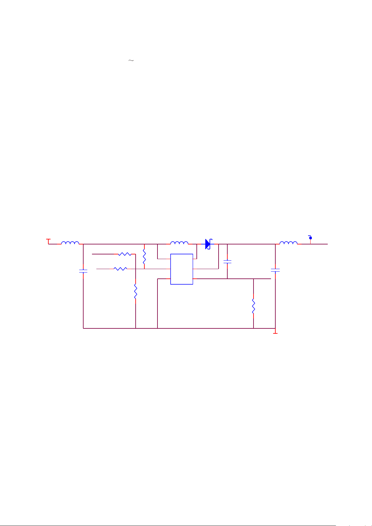
3.2.12 Power management module
1. Function of power management module is to provide 3.3V and 1.8V voltage for the player’s
normal working, shown in the picture 3.2.12.1, 3.2.12.2:
VB
C91
106/X5R
P_GND
R98
68K
EN
U16
1
VIN
2
GND
EN3BYPASS
TPS7 9 3 33
P_GND
C93
102
VOUT
T
S
O
5
4
23-6
C4
103
P_GND
VCC
VCC
Figure 3.2.12.1 3.3V power circuit diagram
- 26 -
Page 32

VDD
C98
101
VDD
C48
106/X5R
D_GND
VDD
C45
106/X5R
U6
1
VI
2
GND
EN3FB
TP S 62 200/FAN5307* SOT23-5
P_GNDP_GND
V_ADJ
2
EN
SW
5
4
R45
L13
CDRH3D16-100
C44
R42
47PF
240K 1%
Q8
MMST3904
D_GND
R43
100K 1%
R44
390K 1%
10k
R46
47k
D_GND
Figure 3.2.12.2 1.8V power circuit diagram
2. Working principle: seen from the circuit diagram, 3.3V power is supplied by IC TPS79333 and
peripheral circuit. TPS79333 is a linear volatge stabilizing module (also called as LDO) and its EN pin is
the enable pin that controls normal working, effective when in high level; BYPASS pin has a resistor
inside, which may constitute low-pass filter together with external 103 capacitor C4 to decrease output
noise.
1.8V power of the player’s working is supplied by TPS62200 and peripheral circuit. TPS62200 is
high-efficience voltage drop DC-DC convertor and EN pin is enable pin, effective when in high. The
relationship between TPS62200 output voltage and FB pin feedback resistance is:
R42
VOUT=0.5
1+
( )
R43
From the above, output voltage is about 1.75V.
3.2.13 Reset circuit
1. Reset circuit supplies reset signals for the player. Reset circuit diagram is shown in the picture
3.2.13.1:
VCC
C19 104
R21
220K
R20
10K
Q3SS8050LT
R56 0R
RESETN
R22
1M
GND
C23
104
Figure 3.2.13.1 Reset circuit diagram
- 27 -
Page 33

2. Working principle: when the player power on, voltage stabilizing circuit begins to work and 3.3V
voltage VCC outputs. Voltage on two sends of capacitor C19 cannot change suddenly, so B electrode of
triode Q3 is low level, Q3 is in cutoff state, RESETN is high level to reset for Rk2608 and display screen.
Meanwhile, VCC charges capacitor C19. When B electrode voltage of Q3 reaches connected voltage,
Q3 is on, VCC is on to ground, RESETN becomes low level and reset of the player finishes. Reset time
is decided by C19 and parameters of resistor R21 and R22.
3.2.14 Power on/off control circuit
1. Power on/off control circuit diagram is shown in the picture 3.2.14.1:
BATT
R93
10M
P_GND
R89
10K R90
10K
47K
R96
2.7M
START
OFF
PLAY/PAUSE2
PLAY
START
C85
P_GND
SFI0402-050E100NP
SFI0402-050E100NP
D_GND
START
D12
1N4148WSR95
R65
10K
P_GND
VCC
Q4
MMST3906
R87
330K
EN
R88
1M
P_GND
1N4148WS
Q7
SS8050LT
D8
R94
100K
Q5
SS8050LT
R92
330K
C87
475/X5R
R97 1M
VCC
R85
100k
D9
1N4148WS
L22
601 DCR<350m¦¸
SW1
C86
HOLD
R58
47K
1
2
3
4
VCC
Figure 3.2.14.1 Power on/off control circuit diagram
2. Working principle: START/PLAY/PAUSE is a group of combination buttons and functions are
different in different working times, decided by software. When the player is in power-off state without
connecting with USB, Q4 is in cutoff state. When power-on button Sw1 is in ON position, START is
pulled down to ground to output low level, Q4 is on, diode D8 is also on, BATT pulls EN up through Q4
and D8, TPS62200 and TPS79333 begin to enter working state to output 1.75V and 3.3V voltage to
suppl power for the entire system. System voltage VCC, VDD and OLED (13V) begin to output, crystal
oscillator Y1 oscillates, reset circuit works, main chip and display screen initialize, OSD appears and
machine begins to work.
When in power-on state, press START/PLAY/PAUSE, Q4 is on and BATT produces a voltage drop
through CE electrode of Q4. Because VCC voltage is normal, the circuit composed through R92, R93,
C87 makes N electrode of D12 keeps 3.3V voltage. D12 cannot be on and it in cutoff state, but after
pressing button, voltage of PLAY/PAUSE pin changes and then inputs to pin 57 of Rk2608 to realize
different functions in different operation interfaces.
- 28 -
Page 34

When the time of pressing PLAY button is more than 1 second but less than 4 seconds, pin 57 of
Rk2608 detects he change of voltage; software decides this signal is power-off signal and then saves
contents of machine; pin 58 outputs high level, D12 is on to make Q7 on, VCC is grounded through CE
electrode of Q7, enable end EN is low level, TPS62200 and TPS79333 stop voltage output and the
player realizes software power-off.
When machine down because of software problem, pressing START/PLAY/PAUSE button more
than 4 seconds may realize firmware power-off. The process is: after pressing button, B electrode of Q4
becomes low level, Q4 is on, BATT charges C87 through CE electrode of Q4 and R93, voltage on
capacitor increases gradually to make Q7 on, VCC is grounded through CE electrode of Q7, enable end
EN is low level, TPS62200 and TPS79333 stop voltage output and the player power off. When loosening
button, BATT makes START pin keeps in high level through R89, R90 to make Q5 on, electric charge
saved in C87 discharges quickly through CE electrode of Q5, R22 and R94 to ensure normal power-on
when pressing START/PLAY/PAUSE button next time.
3.2.15 MIC circuit
1. MIC circuit diagram is shown in the picture 3.2.15.1:
MICBIAS
R27
MIC1
1
2
MICROPHONE
Figure 3.2.15.1 MIC circuit diagram
2.2K
R6
47K
C37
221
C7
MIC
105
2. Working principle: MIC circuit is mainly composed of microphone and MIC bias circuit. MIC1
switches the recorded external voice signals into electric signals to input to ADC circuit of Wm8750 and
switches analog signals into digital signals to form WAV file through software encoding to save inside
FLASH. R27 in circuit is bias resistor of microphone, R6 and C37 constitute filtering circuit to filter the
clutter of audio signals.
- 29 -
Page 35

Section Three Servicing Cases
3.3.1 Servicing cases
[ Example 1 ] Symptom: power not on.
Description: no OSD and no output.
Analysis and troubleshooting: firstly confirm whether it is caused by battery or power circuit.
Connect with computer and check whether display screen has display. Power on, connect and there is
no display. Take the player apart and check. Firstly test power supply voltage and it cannot be lower than
3.2V. Use multimeter to test between anode and cathode of battery and then check VCC3.3V and 1.8V
that output through BGA. During the checking, we find that 3.3V is normal and 1.8V is normal. When
pressing ON button in normal working, after testing actually, VCC1.8V should be pulled down to about
1.7V, which is normal. When working normally, VCC3.3V should be slightly lower to 3.1--3.2V, which is
normal. Then test crystal oscillator X1 and oscillation is normal. The frequency is 12MHZ and it is
11.999MHZ after testing actually. Reset is also normal, so we finally judge that main decode chip has
trouble. Change chip Rk2608 and upgrade software again. Power on and trouble is removed.
[ Example 2 ] Symptom: power not on.
Description: no OSD and no output.
Analysis and troubleshooting: firstly confirm whether it is caused by battery or power circuit.
Connect with power adapter and check whether charge is available and whether screen has display.
After power on and connecting, there is no display. After taking machine apart, firstly test power supply
3.3V and 1.8V and we find 3.3V is normal. Then test 1.8V and voltage on two ends of L13 and find that
1.8V only has 0.7V. Observe DC-DC switch IC U6 carefully and find that pin 4 feedback has rosin joint.
After welding again, trouble is removed.
[ Example 3 ] Symptom: machine not power on.
Description: after pressing ON button, screen has no display and headphone has no output.
Analysis and troubleshooting: connect Mp4 player with computer and there is no display. Test
charge current and find that current is large. Open machine casing to test and current is normal. Power
on again and it is normal, so we preliminarily judge that short-circuit in a certain position causes the
trouble. Observe carefully and find that two lead wires of buzzer have been damaged to cause the inner
part show outside and short-circuit with bottom casing, which makes working current of the player large.
After installing battery, machine cannot power on. Change buzzer lead wire, test and trouble is removed.
- 30 -
Page 36

[ Example 4 ] Symptom: noise when tuning.
Description: radio station has noise when tuning.
Analysis and troubleshooting: firstly judge whether the tuning components or common part has
trouble. Listen to radio station by using headphone and check whether only one side of headphone has
sound and the result is normal. Then switch in tuning state to search radio station automatically and the
result is normal, which means power supply, data and clock are normal. To remove interferences from
outside, we receiver the nearest radio station to listen and check whether it is clear, and it has noise in
result. The circuit that causes noise is mainly high frequency tuning and mixed frequency part. Check
carefully and find that pin 37 of U1 (TEA5767HN) has false welding. After welding again, trouble is
removed.
[ Example 5 ] Symptom: no sound when pressing button.
Description: no click sound when pressing buttons.
Analysis and troubleshooting: if no click sound when pressing buttons, firstly check whether sound
of pressing button has been opened. After confirming it is opened, check whether buzzer is normal. Use
resistance level of multmeter to test and the resistance is ten-ohm and more, which is normal. Check J3
end voltage 1.6V and it is normal. When pressing buttons, test DIDI signals and find there is no change.
Check whether crystal oscillator U10 oscillates normally and there is no oscillation. After changing U10,
trouble is removed.
[ Example 6 ] Symptom: no OSD.
Description: screen has no display.
Analysis and troubleshooting: firstly confirm whether power or display screen itself has trouble.
Power on, listen to playing sound and it is normal, so we preliminarily decide power supply 3.3V and
1.8V are normally basically. Test voltage on two ends of L10 and it is about 4.3V, which is normal. Then
test voltage on two ends of D8 and find the anode does not form 13V. Take out display screen and there
is still no 13V. Check input end voltage and EN enable end is normal. Then check feedback pin FB end
voltage and it is low obviously and EN enable end has false welding. After welding again, trouble is
removed.
[ Example 7 ] Symptom: machine down when playing MP4.
Description: machine down when playing video files.
Analysis and troubleshooting: firstly confirm whether machine is normal when playing Mp3. If it is
normal, we can decide power supply, reset and oscillation are normal. Check data and image processing
IC and we preliminarily judge that it is not related to image processing but related to data and address.
Picture information buffers and it is mainly processed through U1. Test power supply 3.3V voltage of U1
and it is normal. Change SDRAM directly and trouble is removed.
- 31 -
Page 37

[ Example 8 ] Symptom: machien down when power on.
Description: after power on, machine down before entering menu operation.
Analysis and troubleshooting: when power on, machine down before entering main menu. Press
PLAY button to power on, when screen appears BBK picture justly, image of the player halts and button
has no function. Firstly test power supply 3.3V, 3.8V and it normal. Then test crystal oscillator oscillation
frequency and it is normal, so we judge that data has abnormality. Because machine down, data cannot
be tested normally. Change main chip and trouble still exists. After changing Flash U4, trouble is
Removed.
[ Example 9 ] Symptom: machine down when tuning.
Description: machine is normal when playing Mp3, Mp4. Machine down when entering tuning state.
Analysis and troubleshooting: firstly check tuning IC power supply 3.3V, and SCL, SDA are normal.
Test whether 32.768 crystal oscillator oscillates normally and whether it has false welding. This crystal
oscillator has direction when changing it, so it cannot be stuck reversely, otherwise machine down will
happen. Test crystal oscillator and we find it has false welding. After welding again, trouble is removed.
Example 10 ] Symptom: computer cannot be connected.
Description: after connecting with computer, no display and disk cannot be found.
Analysis and troubleshooting: firstly confirm whether charge is available and it is normal after
power on. Use diode level of multimeter to test the resistance value to ground of D+, D- data signals in
USB terminal position and it should be close to several hundred ohm. Then test between D+ and D- and it
should not have short-circuit. Test DP and DM and they are normal. Test power supply 3.3V, 1.8V and it
is normal. Crystal oscillator oscillates normally. Change chip Rk2608, upgrade software again, connect
with computer and trouble is removed.
- 32 -
Page 38

3.3.2 Troubleshooting diagram
1. Troubleshooting flow chart for “No OSD” is shown in the picture 3.3.2.1:
No OSD
Whether
D3 anode 12V voltage
is normal
Y
Whether there is 12V
voltage on display
screensocket
Y
Whether 3.3V
power supply is normal
Y
Whether it is
normal after changing
display screen
components
Y
N
Check DC-DC boost circuit
and peripheral elements
N
Check whether display screen
flat cable holderhas false welding
N
Display screen flat cable
holder has false welding
N
Display screen flat cable
holder has trouble
Whether 8-digit number
of screen is normal
Y
Change display screen
components
N
Change decode chip
Figure 3.3.2.1 Troubleshooting diagram for “No OSD”
- 33 -
Page 39

2. Troubleshooting flow chart for “USB is not connected” is shown in the picture 3.3.2.2:
USB is not connected
Check whether 5V
of Q2 is grounded
normally
Y
Check whether 3.3V
and 1.8V are normal
whether oscillation
of 12M crystal oscillator
D+, D- resistance
software upgrading is
Y
Check
is normal
Y
Check
to ground
Y
Whether
available
N
Q2 has trouble or USB
socket has rosin joint
N
Check each DC-DC switch
circuit and peripheral elements
N
Change crystal oscillator
or capacitor n two sides
N
Check whether T1 or USB
socket has rosin joint
N
Change the main decode
chip
Y
Upgrade software
Figure 3.3.2.2 Troubleshooting diagram for “USB is not
- 34 -
Page 40

3. Troubleshooting fow chart for “Do not charge” is shown in the picture 3.3.2.3:
Do not charge
Whether
battery is fully
charge with voltage
4.2V-4.3V
Y
Battery
is fully charged,
then protection
Y
Normal after discharge
Figure 3.3.2.3 Troubleshooting diagram for “Do not charge”
N
whether USB_VBUS
has 5V voltage
Whether
BAT voltage has
change
Battery components have
trouble change battery or
battery holder
Check
Y
N
Check power supply circuit
Y
N
Change IC ISL6294
- 35 -
Page 41

4. Troubleshooting flow chart for "Power not on" is shown in the picture 3.3.2.4:
Power not on
Check charge circuit
Check U16 and peripheral
circuit
Check U6 and peripheral
circuit
Whether battery
voltage is lower than
3.4V
Y
N
Whether battery
voltageis up to 3.6V
after charge
Y
N
N
whether U6 outputs 1.8V
Refer to troubleshooting
process for "Machine not
power on"
Check
whether U16 outputs
3.3V normally
Y
Check
normally
Y
N
Whether there is OSD
after connecting with
Whether U16 input
pin voltage is up to
BGA has trouble
computer
Y
5V
Y
N
Change battery components
N
Check D5 and Q2
Figure 3.3.2.4 Troubleshooting diagram for “Power not on”
- 36 -
Page 42

5. Troubleshooting flow chart for “Machine not power on” is shown in the picture 3.3.2.5:
Machine not power on
Change crystal oscillator
Check reset circuit
Whether
3.3V, 1.8V voltage output
is normal
Y
N
N
Whether
crystal oscillator Y1
has normal
oscillation
Y
Whether
reset circuit is normal
Y
Change the main decode
chip
Whether
N
software upgrading
is available after connecting
with computer
Whether
it is normal
after upgrading
software
Trouble is removed
Check USB terminal welding
N
A
Y
N
Change the main decode
chip
Y
A
Test
N
whether DM,
DP resistance to
ground is
normal
Y
Change the main decode
chip
Figure 3.3.2.5 Troubleshooting diagram for “Machine not
- 37 -
Page 43

Section Four Signal waveform diagram
This section collects signal waveform diagram of audio, video and each unit circuit with the purpose
To help servicing personnel to judge where trouble lies in accurately and quickly to improve servicing
skills. For the difference of oscillograph's type, model and tuner, a certain difference may exist, so the
servicing personnel are expected to pay more attention to check in daily operation.
1. Battery voltage BAT1 waveform diagram.
2. VDD waveform diagram
- 38 -
Page 44

3. VCC waveform diagram
4. Display screen background light BCLK waveform diagram
5. PLAY1 waveform diagram when playing.
- 39 -
Page 45

6. OUT_R waveform diagram when playing musical files.
7. OUT_L waveform diagram when playing musical files.
8. Crystal oscillator Y1 waveform diagram
- 40 -
Page 46

9. U6 DC-DC switch waveform diagram
10. Power-on reset RESETN waveform diagram
11. Crystal oscillator XT1 waveform diagram
- 41 -
Page 47

Section Five Function Introduction to IC
3.5.1 Function introduction to HY57V641620E
1. Description
The Hynix HY57V641620E(L/S)T(P) series is a 67,108,864bit CMOS Synchronous DRAM, ideally
suited for the memory applications which require wide data I/O and high bandwidth. HY57V641620E
(L/S)T(P) is organized as 4banks of 1,048,576x16.
HY57V641620E(L/S)T(P) is offering fully synchronous operation referenced to a positive edge of the
clock. All inputs and outputs are synchronized with the rising edge of the clock input. The data paths are
internally pipelined to achieve very high bandwidth. All input and output voltage levels are compatible with
LVTTL.
Programmable options include the length of pipeline (Read latency of 2 or 3), the number of
consecutive read or write cycles initiated by a single control command (Burst length of 1,2,4,8 or full page),
and the burst count sequence(sequential or interleave). A burst of read or write cycles in progress can be
terminated by a burst terminate command or can be interrupted and replaced by a new burst read or write
command on any cycle. (This pipelined design is not restricted by a '2N' rule).
2. Features
◆ Voltage : VDD, VDDQ 3.3V supply voltage
◆ All device pins are compatible with LVTTL interface
◆ 54 Pin TSOPII (Lead or Lead Free Package)
◆ All inputs and outputs referenced to positive edge of system clock
◆ Data mask function by UDQM, LDQM
◆ Internal four banks operation
◆ Auto refresh and self refresh
◆ 4096 Refresh cycles / 64ms
◆ Programmable Burst Length and Burst Type
- 1, 2, 4, 8 or full page for Sequential Burst
- 1, 2, 4 or 8 for Interleave Burst
◆ Programmable /CAS Latency ; 2, 3 Clocks
◆ Burst Read Single Write operation
- -
42
Page 48

3. PIN Description
SYMBOL TYPE DESCRIPTION
CLK Clock
CKE Clock Enable
CS Chip Select Enables or disables all inputs except CLK, CKE, UDQM and LDQM
BA0, BA1 Bank Address
A0 ~ A11 Address
RAS, CAS, WE
UDQM, LDQM
DQ0 ~ DQ15 Data Input/Output Multiplexed data input / output pin
VDD/VSS Power Supply/Ground Power supply for internal circuits and input buffers
VDDQ/VSSQ
Row Address Strobe, Column
Address Strobe, Write Enable
Data Input/Output Mask Controls output buffers in read mode and masks input data in write mode
Data Output Power/Ground Power supply for output buffers
The system clock input. All other inputs are registered to the SDRAM on the
rising edge of CLK
Controls internal clock signal and when deactivated, the SDRAM will be one
of the states among power down, suspend or self refresh
Selects bank to be activated during RAS activity Selects bank to be
read/written during CAS activity
Row Address : RA0 ~ RA11, Column Address : CA0 ~ CA7 Auto-precharge
flag : A10
RAS, CAS and WE define the operation Refer function truth table for details
NC No Connection No connection
3.5.2 Function introduction to RK2608
1. Features
◆ 128 pins LQFP package
◆ Typical power voltage 3.3V(IO), 1.8V(Core)
◆ Use one 24MHz crystal oscillator
◆ 38 GPIO (8bits P0,P1,P3,14bits P2)
◆ 10-bit low resolution ADC with 4-channel Analog Input
◆ Build in Stereo 24-bit Delta-Sigma DAC with on-chip headphone amplifier
◆ Build in Stereo 16-bit Sigma-Delta ADC (Line-in /FM Input/ Microphone with analog mixer)
◆ 40 levels digital volume control
◆ Support external CODEC through I2DSP interface
◆ Support I2C interface
◆ Support USB 2.0 high speed and full speed
◆ Integrated 3 Channel DMA
◆ Embedded DSP Core:
· 4K words Boot Sync ROM
- -
43
Page 49

· 56K words Program Sync SRAM
· 48K words Data Sync SRAM
· 2K words Register Space for Peripherals
· Upgradable firmware through USB/Flash interface
◆ Memory interface:
· External up to 4(cs) x 64M-4G bytes Nand type Flash accessed by DMA
· Support both 8-bit (X8 device) and 16-bit (X16 device) IO bus
· support Toshiba/ Hynix/ Infineon/ Micron/ ST Nand flash memory
· Support 2048+64 / 512+16 bytes per page
· Support various Samsung SmartMedia Cards and their listed commands
· Support SDRAM
· Support SD/MMC
◆ Video Driver: Support TFT LCD/ OLED Interface
◆ Pulse Width Modulators for EL backlights
◆ Support watchdog timer
◆ DSP-based Software:
· MPEG1/2/2.5 Audio Layer 1, 2, 3 decoding, Layer3 encoding
· WMA 9 decoding (RK2608A only)
· G.729 based voice recording and playback
· Equalizer (RK2608A only)
· MPEG-4 @QVGA decoding
· Digital photo frame application software (RK2609A only)
◆ Headphone driver output 2x9mW @32 Ohm(TYP) ; SNR: 90dB (DAC TYP)
· Low Power Consumption, <100mW at typical MP3 decoder solution
2. PIN Description
PIN No. Symbol I/O Description
1 RREF I
2 AGND P
3 DM A I/O
4 DP A I/O
Reference Resistor input
Analog GND
USB data minus
USB data plus
5 VCCA P
6 D0 I/O Pull up Flash/ LCD/ SDRAM data bus bit 0
7 D1 I/O Pull up
8 D2 I/O Pull up
9 D3 I/O Pull up
- -
44
Analog 3.3V power input
Flash/ LCD/ SDRAM data bus bit 1
Flash/ LCD/ SDRAM data bus bit 2
Flash/ LCD/ SDRAM data bus bit 3
Page 50

10 D4 I/O Pull up
Flash/ LCD/ SDRAM data bus bit 4
11 D5 I/O Pull up
12 D6 I/O Pull up
13 D7 I/O Pull up
14 RD/BY I, Pull up
15 FREN O
16 FWEN O
17 FWP O
18 VDD P
19 VSSD P
20 VCC P
21 P2.4/A0 I/O
22 P2.5/A1 I/O
23 P2.6/A2 I/O
24 P2.7/A3 I/O
25 A4 O
Flash/ LCD/ SDRAM data bus bit 5
Flash/ LCD/ SDRAM data bus bit 6
Flash/ LCD/ SDRAM data bus bit 7
Flash ready/busy signal
Flash read enable
Flash write enable
Flash write protect
Digital Core power(1.8V)
Digital Core Ground
I/O POWER(3.3V)
SDRAM/ SRAM Address Bit 0,GPIO
SDRAM/ SRAM Address Bit 1 GPIO; FALE/LCDRS
SDRAM/ SRAM Address Bit 2 GPIO; FCLE
SDRAM/ SRAM Address Bit 3,GPIO
SDRAM/ SRAM Address Bit 4
26 A5 O
27 A6 O
28 A7 O
29 A8 O
30 A9 O
31 A10 O
32 A11 O
33 A12 O SDRAM Address Bit 12 SRAM Address Bit 11
34 BA0 O SDRAM Bank Address 0 SRAM Address Bit 12
35 BA1 O SDRAM Bank Address 1 SRAM Address Bit 13
36 CKE O SDRAM clock enable to SDRAM
37 CLK O system clock to SDRAM
38 P2.8/WEN I/O
39 P2.9/CASN I/O
40 P2.10/RASN I/O
SDRAM/ SRAM Address Bit 5
SDRAM/ SRAM Address Bit 6
SDRAM/ SRAM Address Bit 7
SDRAM/ SRAM Address Bit 8
SDRAM/ SRAM Address Bit 9
SDRAM Address Bit 10
SDRAM Address Bit 11 SRAM Address Bit 10
SDRAM write enable GPIO
SDRAM column address strobe GPIO
SDRAM row address strobe GPIO
41 P2.11/CSN I/O
42 VSSD P Digital Ground
- -
45
SDRAM chip strobe GPIO
Page 51

43 P2.13/PWM0 I/O GPIO/ PWM output0
44 P2.0/SDDO I/O
45 P2.1/SDDI I/O
46 P2.2/SDCLK I/O SD/MMC Clock output
47 P2.3/SDCS I/O SD/MMC chip select output
48 VCC P
49 VSSD P
50 VDD P
51 P0.0 I/O Pull up
52 P0.1 I/O Pull up
53 P0.2 I/O Pull up GPIO, External int2
54 P0.3 I/O Pull up GPIO, External int3
55 P0.4 I/O Pull up & EN GPIO
56 P0.5 I/O Pull up & EN GPIO
57 P0.6 I/O Pull up & EN GPIO
58 P0.7 I/O Pull up & EN GPIO
SD/MMC Data output, Rock2 as input Connect to SD/MMC SDDO
SD/MMC Data input, Rock2 as output Connect to SD/MMC SDDI
I/O POWER(3.3V)
Digital Ground
Digital Core power(1.8V)
GPIO, External int0
GPIO, External int1
59
60
61
62
63
64
65
66 AIL1 I L-channel single-end input 1
67 AIR1 I R-channel single-end input 1
68 AIL2 I L-channel single-end input 2
69
70
71 IREF O Bias current reference of CODEC
P1.1/ I2C_SDA
P1.2/ I2C_SCL
P1.3/ I2SMCLK
P1.4
DAC_LRCK
P1.5/
ADC_LRCK
P1.6/ SDI I/O Pull up & EN GPIO, SDI Data input Connect to SDO of External CODEC
P1.7/ SDO
AIR2 I R-channel single-end input 2
MIC
I/O Pull up & EN
I/O Pull up & EN
I/O Pull up & EN
I/O Pull up & EN
I/O Pull up & EN
I/O Pull up & EN GPIO, SDO Data output Connect to SDI of External CODEC
I Mic single-end analog input
GPIO, External SDA of I2C
GPIO, External SCL of I2C
GPIO, I2SMCLK of External CODEC
GPIO, DAC LRCK of External CODEC
GPIO, ADC LRCK of External CODEC
72 VCOM O Internal biasing voltage for CODEC
73 VSSA P Negative power supply for CODEC
74 VDDA P Positive power supply for CODEC
- -
46
Page 52

75 AOL O L-channel single ended analog output
76 VSSAO P Negative power supply to output amplifiers
77 AOM O Common mode analog output
78 AOMS I Common mode sense input
79 VDDAO P Positive power supply to output amplifiers
80 AOR O R-channel single ended analog output
81 HP_SENSE I Sense of jack insertion
82 VDD P
83 VCC P
84 VSSD P
85 IBOOT I, Pull up Boot select, (Internal 100K pull up)
86 A16 O SRAM Address Bit 16
87 A17 O SRAM Address Bit 17
88 A18 O SRAM Address Bit 18
89 A19 O SRAM Address Bit 19
90 A20 O SRAM Address Bit 20
91 DQM0 O SDRAM DQM0
92 DQM1 O SDRAM DQM1
93 A14 O SRAM Address Bit 14
94 A15 O SRAM Address Bit 15
95 VSSD P LDO33 ground
96 VCC33 P LDO33 3.3V power rail
Digital Core power(1.8V)
I/O POWER(3.3V)
Digital Ground
97 VBAT42 P LDO33 Power input
98 VCC33 P Voltage output
99 VSSD G LDO33 ground
100
101 REXT100K I
102 LRADC3 I Low resolution ADC input3
103 LRADC2 I Low resolution ADC input2
104 LRADC1 I Low resolution ADC input1
105 LRADC0 I Low resolution ADC input0
106 VDDPLL P Analog power of PLL
107 VSSPLL P Analog GND of PLL
- -
VCCA P
ADC 3.3V power input,ADC reference
ADC reference Resistor input
47
Page 53

108 XIN I, OSC
109 XOUT O, OSC Crystal 24MHz OSC output PAD
Crystal 24MHz OSC input PAD
110 VDD P
111 VSSD G
112 VCC P
113 RESET I, Pull up System reset pin, low enable
114 TEST I, Pull down Test mode, ( Internal 100K pull down)
115
116 D8/P3.0 I/O
117 D9/P3.1 I/O
118 D10/P3.2 I/O
119 D11/P3.3 I/O
120 D12/P3.4 I/O
121 D13/P3.5 I/O
122 D14/P3.6 I/O
123 D15/P3.7 I/O
124 LCDRDN O LCD Read execution pin
P1.0/ NORCSN
I/O Pull up & EN
Flash/ LCD/ SDRAM data bus bit 10 GPIO
Flash/ LCD/ SDRAM data bus bit 11 GPIO
Flash/ LCD/ SDRAM data bus bit 12 GPIO
Flash/ LCD/ SDRAM data bus bit 13 GPIO
Flash/ LCD/ SDRAM data bus bit 14 GPIO
Flash/ LCD/ SDRAM data bus bit 15 GPIO
Digital Core power(1.8V)
Digital Ground
I/O POWER(3.3V)
GPIO, NOR FLASH Chip select
Flash/ LCD/ SDRAM data bus bit 8 GPIO
Flash/ LCD/ SDRAM data bus bit 9 GPIO
125 LCDWRN O LCD Write execution pin
126 LCDCSN O LCD driver chip select
127 FCE0 O Flash chip select 0
128 VDDA P
Analog 1.8V power output, Connect one external 10uF CAP
3.5.3 Function introduction to RT9284B
1. Description
The RT9284A/B is a compact, high efficient and high integration LED driver. Internal 22V MOSFET
can support 2 to 5 White LEDs for backlighting and camera flashing.
Highly integration and internal compensation network minimizes as 5 external component counts.
Optimized operation frequency can meet the requirement of small LC filters value and low operation
current with high efficiency. Internal soft start function can reduce the inrush current. Tiny package type of
TSOT-23-5 and TSOT-23-6 packages provide the best solution for PCB space saving and total BOM cost.
2. Features
◆ VIN Operating Range : 2.7V to 5.5V
◆ Maximum Output Voltage up to 20V
- -
48
Page 54

◆ Dimming with Zero-inrush and Wide Frequency Range of 100 to 100kHz
◆ Over Voltage Protection
◆ Output Current up to 100mA at VOUT = 12V.
◆ Zero Shutdown Supply Current
◆ Minimize the External Component
◆ Small LC Filter
◆ Internal Soft Start
◆ RoHS Compliant and 100% Lead (Pb)-Free
3. PIN Description
PIN No. Symbol I/O Description
1 LX O
2 GND
3
4
5
6
FB
EN
OVP
VDD
I
I
I
I Supply Input Voltage Pin
Feedback Reference Voltage Pin
Switch Pin
Ground Pin
Chip Enable (Active High)
over voltage protection
3.5.4 Function introduction to TPS62200
1. Description
The TPS6220x devices are a family of high-efficiency synchronous step-down converters ideally
suited for portable systems powered by 1-cell Li-Ion or 3-cell NiMH/NiCd batteries. The devices are also
suitable to operate from a standard 3.3-V or 5-V voltage rail.
With an output voltage range of 6.0 V down to 0.7 V and up to 300 mA output current, the devices are
ideal to power low voltage DSPs and processors used in PDAs, pocket PCs, and smart phones. Under
nominal load current, the devices operate with a fixed switching frequency of typically 1 MHz. At light load
currents, the part enters the power save mode operation; the switching frequency is reduced and the
quiescent current is typically only 15 µA; therefore it achieves the highest efficiency over the entire load
current range. The TPS6220x needs only three small external components. Together with the tiny SOT23
package, a minimum system solution size can be achieved. An advanced fast response voltage mode
control scheme achieves superior line and load regulation with small ceramic input and output capacitors.
2. Features
◆ High Efficiency Synchronous Step-Down Converter With up to 95% Efficiency
◆ 2.5 V to 6.0 V Input Voltage Range
- -
49
Page 55

◆ Adjustable Output Voltage Range From 0.7 V to VI
◆ Fixed Output Voltage Options Available
◆ Up to 300 mA Output Current
◆ 1 MHz Fixed Frequency PWM Operation
◆ Highest Efficiency Over Wide Load Current Range Due to Power Save Mode
◆ 15-µA Typical Quiescent Current
◆ Soft Start
◆ 100% Duty Cycle Low-Dropout Operation
◆ Dynamic Output-Voltage Positioning
◆ Available in a Tiny 5-Pin SOT23 Package
3. PIN Description
PIN No. Symbol I/O Description
1
2
3
4
5
VI
GND
EN
FB
SW
I
I
I
I/O
Supply voltage pin
Ground
The enable pin of the device
The feedback pin of the device
The switch pin
3.5.5 Function introduction to MCP73832
1. Description
The MCP73831/2 devices are highly advanced linear charge management controllers for use in
space-limited, cost-sensitive applications. The MCP73831/2 are available in an 8-Lead, 2 mm x 3 mm
DFN package or a 5-Lead, SOT23 package. Along with their small physical size, the low number of
external components required make the MCP73831/2 ideally suited for portable applications. For
applications charging from a USB port, the MCP73831/2 adhere to all the specifications governing the
USB power bus.
The MCP73831/2 employ a constant-current/constantvoltage charge algorithm with selectable
preconditioning and charge termination. The constant voltage regulation is fixed with four available options:
4.20V, 4.35V, 4.40V or 4.50V, to accommodate new, emerging battery charging requirements. The
constant current value is set with one external resistor. The MCP73831/2 devices limit the charge current
based on die temperature during high power or high ambient conditions. This thermal regulation optimizes
the charge cycle time while maintaining device reliability.
2. Features
- -
50
Page 56

◆ Linear Charge Management Controller:
· Integrated Pass Transistor
· Integrated Current Sense
· Reverse Discharge Protection
◆ High Accuracy Preset Voltage Regulation: + 0.75%
◆ Four Voltage Regulation Options:
· 4.20V, 4.35V, 4.40V, 4.50V
◆ Programmable Charge Current
◆ Selectable Preconditioning
◆ Selectable End-of-Charge Control
◆ Charge Status Output
· Tri-State Output - MCP73831
· Open-Drain Output - MCP73832
◆ Automatic Power-Down
◆ Thermal Regulation
◆ Temperature Range: -40°C to +85°C
◆ Packaging:
· 8-Lead, 2 mm x 3 mm DFN
· 5-Lead, SOT23
3.5.6 Function introduction to TEA5767HN
1. Description
The TEA5767HN is a single-chip electronically tuned FM stereo radio for low-voltage application with
fully integrated IF selectivity and demodulation. The radio is completely adjustment-free and only requires
a minimum of small and low cost external components. The radio can be tuned to the European, US and
Japanese FM bands.
2. Features
◆ High sensitivity due to integrated low-noise RF input amplifier
◆ FM mixer for conversion to IF of the US/Europe (87.5 to 108 MHz) and Japanese (76 to 91MHz)
FM band
◆ Preset tuning to receive Japanese TV audio up to 108 MHz
◆ RF Automatic Gain Control (AGC) circuit
◆ LC tuner oscillator operating with low cost fixed chip inductors
◆ FM IF selectivity performed internally
◆ No external discriminator needed due to fully integrated FM demodulator
- -
51
Page 57

◆ Crystal reference frequency oscillator; the oscillator operates with a 32.768 kHz clock crystal or
with a 13 MHz crystal and with an externally applied 6.5 MHz reference frequency
◆ PLL synthesizer tuning system
◆ I2C-bus and 3-wire bus, selectable via pin BUSMODE
◆ 7-bit IF counter output via the bus
◆ 4-bit level information output via the bus
◆ Soft mute
◆ Signal dependent mono to stereo blend [Stereo Noise Cancelling (SNC)]
◆ Signal dependent High Cut Control (HCC)
◆ Soft mute, SNC and HCC can be switched off via the bus
◆ Adjustment-free stereo decoder
◆ Autonomous search tuning function
◆ Standby mode
◆ Two software programmable ports
◆ Bus enable line to switch the bus input and output lines into 3-state mode
◆ Automotive temperature range (at VCCA, VCC(VCO) and VCCD = 5 V).
3. PIN Description
PIN No. Symbol I/O Description
1 n.c. not connected
2 CPOUT O charge pump output of synthesizer PLL
3 VCOTANK1 O voltage controlled oscillator tuned circuit output 1
4 VCOTANK2 O voltage controlled oscillator tuned circuit output 2
5 VCC(VCO) P voltage controlled oscillator supply voltage
6 DGND digital ground
7 VCCD P digital supply voltage
8 DATA I/O bus data line input/output
9 CLOCK I bus clock line input
10 n.c. not connected
11 WRITE/READ I write/read control input for the 3-wire bus
12 BUSMODE I bus mode select input
13 BUSENABLE I bus enable input
14 SWPORT1 software programmable port 1
15 SWPORT2 software programmable port 2
16 XTAL1 I crystal oscillator input 1
- -
52
Page 58

17 XTAL2 I crystal oscillator input 2
18 PHASEFIL phase detector loop filter
19 PILFIL pilot detector low-pass filter
20 n.c. not connected
21 n.c. not connected
22 VAFL O left audio frequency output voltage
23 VAFR O right audio frequency output voltage
24 TMUTE I time constant for soft mute
25 MPXO O FM demodulator MPX signal output
26 Vref P reference voltage
27 TIFC I time constant for IF centre adjust
28 LIMDEC1 I decoupling IF limiter 1
29 LIMDEC2 I decoupling IF limiter 2
30 n.c. not connected
31 n.c. not connected
32 Igain I gain control current for IF filter
33 AGND analog ground
34 VCCA P analog supply voltage
35 RFI1 I RF input 1
36 RFGND RF ground
37 RFI2 I RF input 2
38 TAGC time constant RF AGC
39 LOOPSW switch output of synthesizer PLL loop filter
40 n.c.
not connected
3.5.7 Function introduction to M41T62
1. Description
The M41T6x Serial Access TIMEKEEPER
oscillator (external crystal controlled). Eight registers are used for the clock/calendar function and are
®
is a low power Serial RTC with a built-in 32.768kHz
configured in binary coded decimal (BCD) format. An additional 8 registers provide status/control of Alarm,
32KHz output, Calibration, and Watchdog functions. Addresses and data are transferred serially via a two
line, bi-dire ctional I2C interface. The built-in address register is incremented automatically after each
WRITE or READ data byte.
- -
53
Page 59

Functions available to the user include a time-of-day clock/calendar, Alarm interrupts (M41T62/65),
32KHz output (M41T64), programmable Square Wave output (M41T62/63/64), and Watchdog output
(M41T63/65). The eight clock address locations contain the century, year, month, date, day, hour, minute,
second and tenths/hundredths of a second in 24 hour BCD format. Corrections for 28-, 29- (leap year), 30and 31-day months are made automatically.
The M41T6x is supplied in a 16-pin QFN.
2. Features
◆ Counters for tenths/hundredths of seconds, seconds, minutes, hours, day, date, month, year, and
century
◆ 32 KHz crystal oscillator integrating load capacitance and high crystal series resistance operation
◆ Oscillator stop detection monitors clock operation
◆ Serial interface supports I2C bus (400kHz)
◆ 350nA timekeeping current @ 3V
◆ Low operating current of 35µA (@400kHz)
◆ Timekeeping down to 1.0V
◆ 1.3V to 4.4V I2C bus operating voltage
◆ 32KHz square wave on power-up to drive a microcontroller in low power mode
◆ Programmable alarm with interrupt function
◆ Accurate programmable watchdog (from 62.5ms to 31 min)
◆ Software clock calibration to compensate deviation of crystal due to temperature
◆ Automatic leap year compensati
◆ Operating temperature of –40 to 85°C
◆ Lead-free 16-pin QFN package
◆ Lithium ion rechargeable operation
3. PIN Description
PIN No. Symbol I/O Description
1 XI I Oscillator input
2 XO O Oscillator output
3, 5 GND
4 SQW I Programmable square wave
6, 7, 8, 12, 13, 15 ,16
9 SDA I/O Serial data input/output
10 SCL I Serial clock input
11 IRQ/OUT O Interrupt or OUT output (open drain)
- -
NC Not Used
54
Page 60

14 VCC P Supply voltage
3.5.8 Function introduction to WM8750BL
1. Description
The WM8750L is a low power, high quality stereo CODEC designed for portable digital audio
applications.
The device integrates complete interfaces to stereo or mono microphones and a stereo headphone.
External component requirements are drastically reduced as no separate microphone or headphone
amplifiers are required. Advanced on-chip digital signal processing performs graphic equaliser, 3-D sound
enhancement and automatic level control for the microphone or line input.
The WM8750L can operate as a master or a slave, with various master clock frequencies including 12
or 24MHz for USB devices, or standard 256fs rates like 12.288MHz and 24.576MHz. Different audio
sample rates such as 96kHz, 48kHz, 44.1kHz are generated directly from the master clock without the
need for an external PLL.
The WM8750L operates at supply voltages down to 1.8V, although the digital core can operate at
voltages down to 1.42V to save power, and the maximum for all supplies is 3.6 Volts. Different sections of
the chip can also be powered down under software control.
The WM8750L is supplied in a very small and thin 5x5mm QFN package, ideal for use in hand-held
and portable systems.
2. Features
◆ DAC SNR 98dB (‘A’ weighted), THD –84dB at 48kHz, 3.3V
◆ ADC SNR 95dB (‘A’ weighted), THD -82dB at 48kHz, 3.3V
◆ Complete Stereo / Mono Microphone Interface
·Programmable ALC / Noise Gate
◆ On-chip 400mW BTL Speaker Driver (mono)
◆ On-chip Headphone Driver
·>40mW output power on 16O / 3.3V
·THD –80dB at 20mW, SNR 90dB with 16O load
·No DC blocking capacitors required (capless mode)
◆ Separately mixed mono output
◆ Digital Graphic Equaliser
◆ Low Power
·7mW stereo playback (1.8V / 1.5V supplies)
·14mW record & playback (1.8V / 1.5V supplies)
◆ Low Supply Voltages
- -
55
Page 61

·Analogue 1.8V to 3.6V
·Digital core: 1.42V to 3.6V
·Digital I/O: 1.8V to 3.6V
◆ 256fs / 384fs or USB master clock rates: 12MHz, 24MHz
◆ Audio sample rates: 8, 11.025, 16, 22.05, 24, 32, 44.1, 48, 88.2, 96kHz generated internally from
master clock
◆ 5x5x0.9mm QFN package
3. PIN Description
PIN NO
1 MCLK Digital Input Master Clock
2 DCVDD Supply Digital Core Supply
3 DBVDD Supply Digital Buffer (I/O) Supply
4 DGND Supply Digital Ground (return path for both DCVDD and DBVDD)
5 BCLK Digital Input / Output Audio Interface Bit Clock
6 DACDAT Digital Input DAC Digital Audio Data
7 DACLRC Digital Input / Output Audio Interface Left / Right Clock/Clock Out
8 ADCDAT Digital Output ADC Digital Audio Data
9 ADCLRC Digital Input / Output Audio Interface Left / Right Clock
10 MONOOUT Analogue Output Mono Output
11 OUT3 Analogue Output Analogue Output 3 (can be used as Headphone Pseudo Ground)
12 ROUT1 Analogue Output Right Output 1 (Line or Headphone)
13 LOUT1 Analogue Output Left Output 1 (Line or Headphone)
14 HPGND Supply Supply for Analogue Output Drivers (LOUT1/2, ROUT1/2)
NAME TYPE DESCRIPTION
15 ROUT2 Analogue Output Right Output 1 (Line or Headphone or Speaker)
16 LOUT2 Analogue Output Left Output 1 (Line or Headphone or Speaker)
17 HPVDD Supply Supply for Analogue Output Drivers (LOUT1/2, ROUT1/2, MONOUT)
18 AVDD Supply Analogue Supply
19 AGND Supply Analogue Ground (return path for AVDD)
20 VREF Analogue Output Reference Voltage Decoupling Capacitor
21 VMID Analogue Output Midrail Voltage Decoupling Capacitor
22 MICBIAS Analogue Output Microphone Bias
23
24 LINPUT3 Analogue Input Left Channel Input 3
25 RINPUT2 Analogue Input Right Channel Input 2
- -
RINPUT3 /
Analogue Input Right Channel Input 3 or Headphone Plug-in Detection
HPDETECT
56
Page 62

26 LINPUT2 Analogue Input Left Channel Input 2
27 RINPUT1 Analogue Input Right Channel Input 1
28 LINPUT1 Analogue Input Left Channel Input 1
29 MODE Digital Input Control Interface Selection
30 CSB Digital Input Chip Select / Device Address Selection
31 SDIN Digital Input/Output Control Interface Data Input / 2-wire Acknowledge output
32 SCLK Digital Input Control Interface Clock Input
3.5.9 Function introduction to XC6206P152MR
1. Description
The XC6206 series are highly precise, low power consumption, high voltage, positive voltage
regulators manufactured using CMOS and laser trimming technologies. The series provides large currents
with a significantly small dropout voltage.
The XC6206 consists of a current limiter circuit, a driver transistor, a precision reference voltage and
an error correction circuit.
The series is compatible with low ESR ceramic capacitors. The current limiter's foldback circuit also
operates as a short protect for the output current limiter and the output pin.
Output voltage can be set internally by laser trimming technologies. It is selectable in 0.1V increments
within a range of 1.2V to 5.0V.
SOT-23 (250mW) and SOT-89 (500mW) packages are available.
2. Features
◆ Maximum Output Current : 250mA (5.0V type)
◆ Dropout Voltage : 160mV @ 100mA (5.0V type)
◆ Maximum Operating Voltage : 6.0V
◆ Output Voltage Range : 1.2V ~ 5.0V (selectable in 0.1V steps)
◆ Highly Accurate : ± 2%
◆ Low Power Consumption : Typ. 1.0µA
◆ Operational Temperature Range : -40OC ~ 85OC
◆ Ultra Small Packages : SOT-23 (250mW), SOT-89 (500mW)
◆ Low ESR Capacitor : Ceramic compatible
- -
57
Page 63

Chapter Four
Assembly and Disassembly Process
In order to get to know the structure of V3more easily and directly, now we use pictures to
present each key point of disassembly and assembly process before all users to prevent users from
operating blindly and to damage elements, so we hope you can operate according to the
instructions strictly.
Note: all operations must be with strict anti-static measures. Operators must wear anti-static
gloves or wrist ring; electric screwdriver must be grounded effectively and articles, such as nippers
must be removed static before using!
4.1 Disassembly process of the player
1. Use cuspidal forceps to take out the LOCK
button.
3. Use a slice with thickness about 0.1mm to in
sert into the gap of the glass prized up and then
peel off glue of the glass slowly to tale out the
glass. Pay attention not to damage touch button
FPC.
2. Insert the forceps into the lock hole and then
prize up one corner of the glass.
4. After peeling off glue of the glass, use nails
to take out the glass.
- 58 -
Page 64

5. Insert the 4 special slice clasp instruments
into the relevant position of the 4 clasps.
6. Use the special hook tool, shown in the
picture,to remove the middle casing.
7. Remove FPC flat cable clasp and then use
forceps to take out FPC flat cable.
9. Use iron to weld to separate the batter and
buzzer lead wire on main board.
8. Use electric screwdriver or “+”-shaped
screwdriver to take out 2 screws of main board.
10. Take out main board components.
- 59 -
Page 65

11. Take out battery components.
13. Take out display screen components from
the direction shown in the picture
4.2 Assembly process of the player
12. Take out the stainless steel cover board
on rear side of display screen.
Assembly process of the player is similar with the disassembly process, and only the sequence is
reverse.
- 60 -
Page 66

Chapter Cinque
PCB board & Circuit diagram
Section One PCB board
5.1.1 Surface layer of Main Board
- 61 -
Page 67

5.1.2 Bottom layer of Main Board
- 62 -
Page 68

FM_3V3
C56 101
FM_ANT
FM_ANT
O603CS
MURATA
COILCRAFT
TOKO SMD
LLQ1608-AR10G
FM_3V3
R69
22R
C68
104
FSGND
A
O603CS
L17
33nH±2%
MURATA
COILCRAFT OR
TOKO SMD
LLQ1608-A33NG
C66 103
L18
33nH±2%
MURATA
COILCRAFT OR
TOKO SMD
LLQ1608-A33NG
R73
22R
D10
BB202
D11
BB202
FM_3V3
FDGND
C76
104
L16
120nH
C57 27PF
FDGND
C59
47PF
R70
100K
FSGND
R68
10K
C65
393
L23 601 DCR<350mΩ
L24
C58
472
40
1
N.C
2
CPOP
3
VCOT1
4
VCOT2
5
VCOVCC
6
DGND
7
DVCC
8
DATA
9
CLOCK
10
N.C
FDGND
601 DCR<350mΩ
38
36
33
31
35
37
32
34
39
N.C
RFI2
TCAGC
LOOPSW
TEA5767HN
NECTAR-IO603CS
W/R11BUSM12BUSEN13SWP114SWP215XTAL116XTAL217PDLF18PHLF19N.C
FM_3V3
I2C_SDA
RFI1
AVCC
RFGND
I2C_SCL
N.C
IFGAI
AGND
TMUTE
20
C60
475/X5R
R67 18K
N.C
DIFL2
DIFL1
TCIFC
VREF
MPXO
RAVO
LAVO
N.C
R66
10R
C61 473
C62 473
C63 473
C64 333
U9
FSGND
30
29
28
27
26
25
24
23
22
21
XT1
32.768KHz
OR 13MHz
CRYSTAL
FDGND
C71
102
C67 333
FSGND
FSGND
FSGND
FSGND
601 DCR<350mΩ
L7
L8
601 DCR<350mΩ
C73
22PF
FDGND FDGND
R72
33K
C74
223
FSGND
FDGND
C72
223
5767R
FDGND
C75
102
VCC
D_GND
L19 1 0UH/2012
C50
105
106/X5R
D_GND
C69
R71
FDGND
0R
FSGNDFDGND
FDGND
FM_3V3
C70
104
63 -
-
Section Two Circuit diagram
Page 69

2SJ-A382-001(HP-DC)
CN1
FM_ANT2
J1
+5V
D-
NC
D+
GND
IN_L
IN_R
GND
3DU05S-32T-10
J2
8
7
6
5
4
3
2
1
K1
K2
K3
K4
K5
K6
1
2
3
4
5
6
7
8
VLED
1
3
4
5
D_GND
L5
601/0603
L1 601/0603
L3 601/0603
R102 0R*
D_GND
C6
D_GND D_GND
Q15
SS8550LT
R81 10K
PSOC_SCL
PSOC_SDA
OUT_R1
SFI0402-050E100NP
L6 680
C8
SFI0402-050E100NP*
D_GND
R82
47K
R74
R75
10K
10K
VCC
OUT_L1
4
5
162
3
RCLAMP0504F/SC-70 6L
GND
D_GND
R5
470R
SS8550LT
Q2
601 DCR<350mΩ
L2
L4
601 DCR<350mΩ
C9
SFI0402-050E100NP*
VCCVLED
LED_CON
R4 100R
R9 100R
D1
D_GND
SCL
R99
1K
C4
104
+5V
SPEAKER_OUTL
SPEAKER_OUTR
R100
1K
C31
220UF/4V
C32 220UF/4V
D_GND
R3
12K
R8
10K
U15
1
P07
2
P05
3
P03
4
P01
5
P27
6
P25
7
P23
8
P21
9
VSS
10
P17
11
P15
12
P13
13
SCL
14
VSS
HP_OUTL
R83
10R
104
C3
USB_VBUS 2
1 3
CY8C21534
HP_OUTR
R84
10R
C92
C90
104
104
USB_DET
T1
SDCW2012-2-900T
2 4
R11
1M
D_GNDD_GND
VDL
28
VDD
27
P06
26
P04
25
P02
24
P00
23
P26
22
P24
21
P22
20
P20
19
XRES
18
P16
17
P14
16
P12
15
SDA
USB_DET 2
R12
1M
VDL
C30
105
GND
K4
K5
K6
K3
K2
K1
SDA
R103
XRES
USB_DM
USB_DP
10K
5767L
5767R
2
2
INT
VCC
R1 100R
R2 100R
HOLD
P1
601 DCR<350mΩ
L20
MCLK#
VCC
R34
10K*
R78 100K
P4
P2
D_GND
BCLK
D_GND
R41
4.7K*
MIC1
1
2
MICROPHONE
R33
0R*
Q6
SS8550LT
R77
4.7K
Q10
MMST3904
D_GND
P5
P6
DBVDD
VCC
C84
104
ADCLRC
DACLRC
DACDAT
ADCDAT
R23 4.7K
I2C_SDA
I2C_SCL
C1
C2 105
R80
4.7K*
VDL
P9 P13
P8
P7P3
C89
106/X5R
105
MICBIAS
R27
2.2K
R6
47K
P10
P11
C37
221
P12
105
C97
U11
104
WM8750
3
DBVDD
2
DCVDD
18
AVDD
17
HPVDD
1
MCLK
5
BCLK
9
ADCLRC
7
DACLRC
6
DACDAT
8
ADCDAT
29
MODE
MONOOUT
30
CSB
31
SDIN
32
SCLK
28
LINPUT1
27
RINPUT1
C7
MIC
P14
LINPUT2
RINPUT2
LINPUT3
RINPUT3
DGND
HPGND
AGND
LOUT2
ROUT2
OUT3
LOUT1
ROUT1
MICBIAS
VREF
VMID
26
25
24
23
4
14
19
16
15
10
11
13
12
22
20
21
DIDI
MIC
SPEAKER_OUTL
SPEAKER_OUTR
D_GND
HP_OUTL VREF
HP_OUTR
C82
104
VREF
106/X5R
MICBIAS
C83
D_GND
R47 10K
R79 4.7K
R91 4.7K
C80
104
105
C51
R48
47K
C78
C81
106/X5R
VCC
D_GND
C52
104
12
C53
105
C79
106/X5R
R49
0R
J3
Q9
MMST3904
105
R31
1K
C54
105
64 -
-
Page 70

R21
220K
R22
1M
C19 104
D_GND
VCC
U1
HY57V641620ETP
1
VDD
D0
2
C35
106/X5R
D1
D2
D3
D4
D5
D6
D7
DQM0
WEN
CASN
RASN
CSN
BA0
BA1
A10
A0
A3
R24 33R
R26 33R
3
4
5
6
7
8
9
10
11
12
13
14
15
16
17
18
19
20
21
22
23
24
25
26
27
BACK_EN
BACK_L
DQ0
VDDQ
NC
DQ1
VSSQ
NC
DQ2
VDDQ
NC
DQ3
VSSQ
NC
VDD
DQM0
WEN
CASN
RASN
CS
BA0
BA1
A10AP
A0
A1
A2
A3
VDD
SDRAM
R50
4.7K
MCLK#
C27
6P
D_GND
R59 1K
VCC
R61
0R*
C18
104
GND
GND
FALE/RS/A1
FCLE/A2
C22
104
D_GND
I2C_SCL
I2C_SDA
MCLK
CLK
L9
601/0603
VB
Á ?8825598虾牛
54
VSS
D15
53
DQ7
52
VSSQ
VDDQ
VSSQ
VDDQ
DQM1
R51
4.7K
R60
10K
D14
51
NC
D13
50
DQ6
49
D12
48
NC
D11
47
DQ5
46
D10
45
NC
D9
44
DQ4
43
D8
42
NC
41
VSS
40
NC
DQM1
39
CLK#
38
CLK
CKE
37
CKE
A12
36
A12
A11
35
A11
A9
34
A9
A8
33
A8
A7
32
A7
A6
31
A6
A5
30
A5
A4
29
A4
28
VSS
D_GND
MCLK#
CLK#
C29
6P
L10
CDRH3D16-100
R63
0R*
RT9284B
MBR0520/SOD123
6
LX1VCC
4
5
EN
OVP
2
3
GND
FB
U3
C46
104
D_GND
C47
104
D_GND
65 -
D3
C5
102
R30
12R±1%
LED-
D_GND
L11
601/0603
C36
106/16V/1206
LEDP
LED+
-
VCC VDD
R15 1M
XOUT
C12
20PF/NPO
GND GND
C15
+
106/X5R
C17
104
DM
DP
D0
D1
D2
D3
D4
D5
D6
D7
RD/BY
FREN
FWEN
FWP
A0
A3
A4
A5
A6
A7
A8
A9
A10
A11
1
2
3
4
5
6
7
8
9
10
11
12
13
14
15
16
17
18
19
20
21
22
23
24
25
26
27
28
29
30
31
32
U2
RREF
AGND
DM
DP
VCCA
D0
D1
D2
D3
D4
D5
D6
D7
RD/BY
FREN
FWEN
FWP
VDD
VSSD
VCC
P2.4/A0
FALE/RS/A1
FCLE/A2
P2.7/A3
A4
A5
A6
A7
A8
A9
A10
A11
A12
GND
R19 10K
GND
VCC
106/X5R
GND
GND
VCC
R20
10K
RESETN
R56 0R
Q3SS8050LT
C23
104
GND
USB_DM2
USB_DP2
+
C20
C21
104
VDD
C24
104
FALE/RS/A1
C28 104
FCLE/A2
VCC
A1233BA0
BA0
LCDWRN
FCE0CKE
LCDCSN
LCDRDN
127
126
128
124
125
FCE0
VDDA
LCDCSN
LCDRDN
LCDWRN
P2.9/CASN39P2.10/RASN40P2.11/CSN41GND42P2.13/PWM043P2.0/SDDO44P2.1/SDDI45P2.2/SDCLK46P2.3FCE1/SDCS47VCC48VSSD49VDD
BA135CKE36CLK37P2.8/WEN
34
38
CSN
CLK
BA1
CASN
WEN
RASN
GND
D15
123
P3.7/D15
BACK_L
Y1
24MHz
D14
D13
121
122
P3.5/D13
P3.6/D14
128-Pin TQFP
DFU
CHG_OK
LED_CON
2
XIN
C13
20PF/NPO
D10
D12
D11
118
119
120
P3.3/D11
P3.4/D12
RK2608
FCE1
VCC
C33
104
GND
C10
104
2
V_ADJ
D9
D8
RESETN
114
112
116
117
113
115
TEST
P3.0/D8
P3.1/D9
RESETN
P3.2/D10
P1.0/NORCSN
P0.3
P0.051P0.1
P0.253P0.455P0.556P0.657P0.758P1.1/I2C_SDA
54
50
52
2
2
INT
HOLD
USB_DET
VDD
C34
104
PSOC_SCL
GND
110
111
VCC
VSSD
BACK_EN
PSOC_SDA
PLAY/PAUSE
VDD
OFF
105
XOUT
109
XOUT
2
C14
GND
XIN
108
107
XIN
VSSPLL
P1.2/I2C_SCL60P1.3/I2SMCLK61P1.4/DAC_LRCLK62P1.5/ADC_LRCLK63P1.6/SDI
59
I2C_SDA
I2C_SCL
MCLK
I2C_SCL
I2C_SDA
2
BATT
BAT_DET
106
105
VDDPLL
LRADC0
DACLRC
R16
100K±1%
R17 100K±1%
2
C38
104
GND
VCC1V8
101
104
103
102
LRADC1
LRADC2
LRADC3
HP_SENSE
64
ADCDAT
ADCLRC
GND
GND
99
100
VSSD
VCCA
REXT100K
VCC33
VSSD
DQM1
DQM0
IBOOT
VSSD
VDDAO
AOMS
AOM
VSSAO
VDDA
VSSA
VCOM
IREF
P1.7/SDO
R18
100K
VCC
+
C16
106/X5R
97
98
GND
088
料号:
VCC33
VBAT42
A15
A14
A20
A19
A18
A17
A16
VCC
VDD
AOR
AOL
MIC
AIR2
AIL2
AIR1
AIL1
3193
96
95
94
93
DQM1
92
DQM0
GND
GND
GND
GND
DACDAT
GND
C26
104
VCC
VDD
C25
104
91
90
89
88
87
86
85
84
83
82
81
80
79
78
77
76
75
74
73
72
71
70
69
68
67
66
65
VCC
NAND Flash
48
NC
47
NC
46
NC
45
NC
44
I/O7
43
I/O6
42
I/O5
41
I/O4
40
NC
39
NC
38
PRE
37
VCC
36
VSS
35
NC
34
NC
33
NC
32
I/O3
31
I/O2
30
I/O1
29
I/O0
28
NC
27
NC
26
NC
25
NC
D7
D6
D5
D4
R55 0R
D3
D2
D1
D0
D_GND
BATT
R76
0R
M41T62
U10
16
NC6NC7NC
14
NC13NC15NC
IRQ11VCC
I2C_SCL
10
SCL
I2C_SDA
9
SDA
SQW
8
4
DIDI
2
VCC
C42
104
C77
6PF*
XT2
1
OSCI
2
OSCO
3
GND
5
GND
OSCO
D_GND
OSCI
32.768KHZ
RD/BY
FREN
FCLE/A2
FALE/RS/A1
FWEN
FWP
1
2
3
4
5
6
7
8
9
10
11
12
13
14
15
16
17
18
19
20
21
22
23
24
U5
RES#
NC
NC
NC
NC
R/B2
R/B1
RE
CE1
CE2
NC
VCC
VSS
NC
NC
CLE
ALE
WE
WP
NC
NC
NC
NC
NC
NAND FLASH
R37
10K
RD/BY
FREN
FCLE/A2
FALE/RS/A1
FWEN
FWP
D_GND
1
2
3
4
5
6
7
8
9
10
11
12
13
14
15
16
17
18
19
20
21
22
23
24
U4
RES#
NC
NC
NC
NC
R/B2
R/B1
RE
CE1
CE2
NC
VCC
VSS
NC
NC
CLE
ALE
WE
WP
NC
NC
NC
NC
NC
NAND FLASH
R36
R35
47K
47K
FCE0
FCE1
VCC
C39 104
GND
R40
47K
NAND Flash
48
NC
47
NC
46
NC
45
NC
44
I/O7
43
I/O6
42
I/O5
41
I/O4
40
NC
39
NC
38
PRE
37
VCC
36
VSS
35
NC
34
NC
33
NC
32
I/O3
31
I/O2
30
I/O1
29
I/O0
28
NC
27
NC
26
NC
25
NC
D7
D6
D5
D4
R32 0R
D3
D2
D1
D0
I2C_SDA
R38 0R
I2C_SCL
VCC VCC
C40
104
R39 0R
C41 104
D_GNDD_GND
CN2
1
2
3
4
5
240*320(RGB)
6
7
8
9
10
11
12
13
14
15
16
17
18
19
20
21
22
23
FALE/RS/A1
24
25
D_GND
26
27
28
28pin
D_GND LCD_3V3
LCDCSN
LCDRDN
D0
D1
D2
D3
D4
D5
D6 LCDCSN
D7 LCDRDN
D8
D10
D11
D12
D13
D14
R29
D15
0R
LCDWRN
LED+
LED-
D_GND
LCD_3V3
RESETN
C49
105
LCDWRND9
FALE/RS/A1
VCC
VCC
R13
R7
R25
R28
10K
10K
10K
10K
L12
601/0603
D_GND
LCD_3V3
C43
105
Page 71

USB_VBUS3
CHG_OK2
R52 0R
VCC
R54
10K
USB_VBUS
D_GND
C96
475
VIN
5V
U8
1
VDD
2
VDD
5
START
NC7VSS
MCP73832T
P_GND
VBAT
PROG
VBAT
R101
1K
4
8
3
6
D_GND
D5
BAT43WS
R14
100R
BAT
G
R53
2.7K±1%
D_GND
VB
P_GND
P_GND
Q1
SI2305DS SOT23
D S
BAT
BAT1
BATT
C99
105
C91
106/X5R
C45
106/X5R
D_GND
R98
68K
P_GND
EN
P_GND
CN3
1
BAT
2
U16
1
VIN
2
GND
EN3BYPASS
TPS79333DBVR SOT23-5
C93
102
P_GND
5
VOUT
4
C94
103
P_GND
USB_VBUS3
C88
SFI0402-050E100NP
VCC
VCC
VCC
C95
106/X5R
P_GND
U6
1
VI
2
GND
3
EN
TPS62200/FAN5307* SOT23-5
V_ADJ
2
D15
1N4148WS
XC6206P152
2
VI
U14
1
GND
EN
VOUT
5
SW
4
FB
R45
10k
3
R46
47k
R86
330K
R64
100K
R44
390K±1%
R87
330K
R88
1M
P_GND
L13
CDRH3D16-100
R42
240K±1%
D_GND
Q8
MMST3904
D_GND
VCC
1N4148WS
Q7
SS8050LT
VCC1V8
R43
100K±1%
D8
R94
100K
Q5
SS8050LT
2
C44
47PF
C98
101
MMST3906
R92
330K
C87
475/X5R
P_GND
VDD
C48
106/X5R
D_GND
BATT
Q4
R97 1M
R93
10M
VDD
P_GND
R89
10K
R95
47K
R96
2.7M
START
D_GND
R90
10K
START
D12
1N4148WS
R65
10K
P_GND
PLAY/PAUSE2
START
C85
SFI0402-050E100NP
SFI0402- 050E100NP
OFF 2
PLAY
P_GND
R10
1K
SW2
DFU
D_GND
P_GND
C86
R57
47K
VCC
VCC
HOLD
R85
100k
D9
1N4148WS
L22
601 DCR<350mΩ
R58
47K
VCC
DFU
SW1
1
2
3
4
SK??
66 -
-
P_GND
A_GND
Page 72

5V
D5
USB_VBUS
USB_VBUS3
BAT43WS
C45
106/X5R
P_GNDP_GND
U6
1
VI
2
GND
3
EN
TPS62200/FAN5307* SOT23-5
SW
FB
5
4
R44
390K±1%
L13
CDRH3D16-100
R42
240K±1%
C44
47PF
R43
100K±1%
VDD
C48
106/X5R
C98
101
D_GND
VDD
USB_VBUS3
C88
SFI0402-050E100NP
P_GND
2
V_ADJ
D15
1N4148WS
R45
10k
R46
47k
R86
330K
Q8
MMST3904
D_GND
D_GND
67 -
-
Page 73

R7,R8,R13,R19,R20,R25,R28,R37,R45,R47,R5
Chapter six BOM List
MATERIAL
CODE
BATTERY PROTECT BOARD 5448893
0090354 SMD RESISTOR 1/16W 470O±5% 0402 R1
0090368 SMD RESISTOR 1/16W 2K±5% 0402 R2
0310480 SMD CAPACITOR 10V 104±10% 5R 0402 C1,C2,C3
0790065
0790090
0882570 IC S-8261AANMG22 SO23-6
1633305 PCB E29-0
MATERIAL NAME SPECIFICATIONS LOCATION
SMD FIELD EFFECT
TRANSISTOR
SMD FIELD EFFECT
TRANSISTOR
ECH8601 TSSOP
ECH8601R TSSOP
U2 ①
U2 ①
V3N video(RU)B SILVER
FPC BOARD 5449972
1633812 FPC 9 3-1
0700186 SMD RADIATION DIODE 1SB0602V22D0CA01
0700187 SMD RADIATION DIODE LTST-S270KRKT RED
D1,D3 ②
D1,D3 ②
0090346 SMD RESISTOR 1/16W 220O±5% 0402 R1,R3
V3N video(RU)B SILVER
MAINBOARD 2V3-1 1.0/Ver3.00 4940141
0090001 SMD RESISTOR 1/16W 0O±5% 0603 L11
0090324 SMD RESISTOR 1/16W 0O±5% 0402 R29,R32,R38,R39,R49,R52,R55,R56,R71,R76
0090326 SMD RESISTOR 1/16W 10O±5% 0402 R66,R83,R84
0090830 PRECISION SMD RESISTOR 1/1612O±1% 0402 R30
0090046 SMD RESISTOR 1/10W 470O±5% 0805 R5
0090447 SMD RESISTOR 1/16W 22O±5% 0402 R73,R69
0090330 SMD RESISTOR 1/16W 33O±5% 0402 R24,R26
0090339 SMD RESISTOR 1/16W 100O±5% 0402 R1,R2,R4,R9,R14
0090362 SMD RESISTOR 1/16W 1K±5% 0402 R10,R31,R59,R99,R100,R101
0090369 SMD RESISTOR 1/16W 2.2K±5% 0402 R27
0090839 PRECISION SMD RESISTOR 1/16W3K±1% 0402 R53
0090377 SMD RESISTOR 1/16W 4.7K±5% 0402 R23,R50,R51,R79,R91
0090385 SMD RESISTOR 1/16W 10K±5% 0402
0090387 SMD RESISTOR 1/1612K±5% 0402 R3
4,R60,R65,R68,R74,R75,R77,R81,R89,R90,R1
- 68 -
Page 74

MATERIAL
CODE
MATERIAL NAME SPECIFICATIONS LOCATION
0090390 SMD RESISTOR 1/16W 18K±5% 0402 R67
0090396 SMD RESISTOR 1/16W 33K±5% 0402 R72
0090400 SMD RESISTOR 1/16W 47K±5% 0402 R6,R35,R36,R40,R46,R48,R57,R58,R82,R95
0090404 SMD RESISTOR 1/16W 68K±5% 0402 R98
0090408 SMD RESISTOR 1/16W 100K±5% 0402 R18,R64,R70,R85,R94,R78
0090421 SMD RESISTOR 1/16W 330K±5% 0402 R86,R87,R92
0090433 SMD RESISTOR 1/16W 1MO±5% 0402 R11,R12,R15,R22,R88,R97
0090509 PRECISION SMD RESISTOR 1/16W 100K±1% 0402 R16,R17,R43
0090417 SMD RESISTOR 1/16W 220K±5% 0402 R21
0090687 PRECISION SMD RESISTOR 1/16W 240K±1% 0402 R42
0090831 PRECISION SMD RESISTOR 1/16390K±1% 0402 R44
0090444 SMD RESISTOR 1/16W 10MO±5% 0402 R93
0090438 SMD RESISTOR 1/162.7MO±5% 0402 R96
1030029
1030033
SMD PRESS SENSITIVITY
RESISTOR
SMD PRESS SENSITIVITY
RESISTOR
SFI0402-050E100NP
S1005H180C100GPT 0402
C6,C85,C86,C88 ③
C6,C85,C86,C88 ③
0310503 SMD CAPACITOR 50V 6P±0.25P NPO 0402 C27,C29
0310416 SMD CAPACITOR 50V 22P±5% NPO 0402 C73
0310418 SMD CAPACITOR 50V 27P±5% NPO 0402 C57
0310424 SMD CAPACITOR 50V 47P±5% NPO 0402 C44,C59
0310432 SMD CAPACITOR 50V 101±5% NPO 0402 C56,C98
0310435 SMD CAPACITOR 50V 221±5% NPO 0402 C37
0310704 SMD CAPACITOR 25V 102±10% 7R 0402 C5,C71,C75,C93
0310706 SMD CAPACITOR 25V 472±10% 7R 0402 C58
0310453 SMD CAPACITOR 25V 103±10% 7R 0402 C94,C66
0310834 SMD CAPACITOR 16V 106±20% 5R 1206 C36
0310455 SMD CAPACITOR 16V 223±10% 7R 0402 C72,C74
0310710 SMD CAPACITOR 16V 333±10% 5R 0402 C64,C67
0310711 SMD CAPACITOR 10V 393±10% 5R 0402 C65
0310712 SMD CAPACITOR 10V 473±10% 5R 0402 C61,C62,C63
C3,C4,C10,C17,C18,C19,C21,C22,C23,C24,C2
0310480 SMD CAPACITOR 10V 104±10% 5R 0402
5,C26,C28,C33,C34,C38,C39,C40,C41,C42,C4
3,C46,C47,C68,C70,C76,C78,C80,C82,C84,C9
0,C92,C97
0310415 SMD CAPACITOR 50V 20P±5% NPO 0402 C12,C13
- 69 -
Page 75

MATERIAL
CODE
0310776 SMD CAPACITOR 6.3V 105±20% 5R 0402 ? ?
0310662 SMD CAPACITOR 6.3V 105±10% 5R 0402
MATERIAL NAME SPECIFICATIONS LOCATION
C1,C2,C7,C14,C30,C50,C51,C52,C53,C54,C99
④
C1,C2,C7,C14,C30,C50,C51,C52,C53,C54,C99
④
0310753 SMD CAPACITOR 16V 104±20% 5R 0402 C49
0310717 SMD CAPACITOR 6.3V 475±20% 5R 0603 C60,C87,C96
0310827 SMD CAPACITOR
0310831 SMD CAPACITOR
6.3V106±20% 5R 0805 T≤0.85
6.3V106±10%5R 0805 T≤0.85
C15,C16,C20,C35,C45,C48,C69,C79,C81,C83,
C89,C91,C95 ⑤
C15,C16,C20,C35,C45,C48,C69,C79,C81,C83,
C89,C91,C95 ⑤
0310736 SMD TANTALUMCAPACITOR 4V 220uF±20% 3528(B) C31,C32
0390354 SMD MAGNETIC BEADS 68O/100MHz±25% 1608 L6
0390388 SMD MAGNETIC BEADS 600O/100MHZ±25% 1005 L2,L4,L7,L8,L20,L22,L23,L24
0390142 SMD MAGNETIC BEADS FC1608-60102 L1,L3,L5,L9,L12
0390221 SMD COIL THREAD INDUCTOR 33nH±2% 1608 L18,L17
0390398 SMD COIL THREAD INDUCTOR 120nH±2% 1608 L16
0390386 SMD CORES INDUCTOR 10uH±20% CDRH3D16/HP L10,L13
0390044 SMD INDUCTOR 10UH±10% 2012 L19
0960278 SMD CRYSTAL OSCILLATOR 24MHz±30ppm 5032/4 20P Y1
0960279 SMD CRYSTAL OSCILLATOR 32.768KHz±20ppm SS6 12.5P XT1,XT2
0680077 SMD SCHOTTKY DIODE MBR0520 SOD123 D3
0680074 SMD SCHOTTKY DIODE B43WS SO323 D5
0700115
SMD TRANSFIGURATION
DIODE
BB202 D10,D11
0700154 SMD TRIODE 14148WS SO323 D8,D9,D12,D15
0780300 SMD TRIODE SS8550LT SO323 Q2,Q6,Q15
0780299 SMD TRIODE SS8050LT SO323 Q3,Q5,Q7
0780298 SMD TRIODE MMS3904 SO323 Q8,Q9,Q10
0780293 SMD TRIODE MMS3906 SO323 Q4
0790041
SMD FIELD EFFECT
TRANSISTOR
SI2305DS SO23 Q1
0883456 IC K9LAG08U0M-PCBO TSOP U4,U5
0883217 IC RT9284B-20PJ6E SOT23-6 U3
0883083 IC CY8C21534 SSOP U15
0882668 IC 79333DBVR SO23-5 U16
0883370 IC MCP73832 DFN U8
0883384 IC XC6206P152MR SOT-23 U14
- 70 -
Page 76

MATERIAL
CODE
MATERIAL NAME SPECIFICATIONS LOCATION
0882850 IC 4162 QFN U10
0883330 IC WM8750BL QFN
0883403 IC WM8750L QFN
0883193 IC R2608 LQFP
0883442 IC RK2608A LQFP
U11 ⑥
U11 ⑥
U2 ⑦
U2 ⑦
08825598 IC HY57V641620ETP-7 TSOP$ U1
0882388 IC TE5767HN HVQFN U9
0882476 IC TP62200 SO23-5 U6
1090080 ESD ELEMENT RCL0504 SC70-6L
1090084 ESD ELEMENT PLR0504P SC70-6L
1310096 SMD STIR SWITCH SSSS70101
1310095 SMD STIR SWITCH 1370R
D1 ⑧
D1 ⑧
SW1 ⑨
SW1 ⑨
1340099 SMD LIGHT TOUCH SWITCH SKRELGE010 SW2
1000053 COMMON MODE FILTER SDCW2012-2-371T NT2012 T1
1980050 EARPHONE SOCKET 2S382-001 CN1
1140082 MICROPHONE 44dB±3dB 4×1.2 WITH NEEDLE
MIC1 ⑩
1140105 MICROPHONE
42dB±2dB 4×1.5 WITH NEEDLE MIC1 ⑩
1860140 USB SOCKET 3DG08S-30G-P J1
1940405 CABLE SOCKET
8P 0.5mm SMD,NEXT MEET WITH
CLASP
J2
1633811 PCB 2 3-1
- 71 -
Page 77

Chapter Four V5
Assembly and Disassembly Process
In order to get to know the structure of V5more easily and directly, now we use pictures to present
each key point of disassembly and assembly process before all users to prevent users from operating
blindly and to damage elements, so we hope you can operate according to the instructions strictly.
Note: all operations must be with strict anti-static measures. Operators must wear anti-static gloves
or wrist ring; electric screwdriver must be grounded effectively and articles, such as nippers must be
removed static before using!
4.1 Disassembly process of the player
1. Use cuspidal forceps to take out the LOCK button;
3. Take out the two screws of button board.
2. Use blade to remove the glass from the
gap on one side of the glass.
4. Push out one corner of bottom casing from the
hole of hanging rope and then separate the bottom
casing from button position.
- 72 -
Page 78

5. Separate the bottom casing and the middle casing.
6. Remove the clasp of button flat cable and
then pull out button flat cable.
7. Take out 2 screws of main board.
9. Use forceps to pull out display screen flat
cable and then take out main board.
8. Take out the main board from middle casing.
10. Use electric screwdriver or “+”-shaped screwdriver
to take out 6 screws of cover board, take out display
screen cover board and then the display screen
components.
4.2 Assembly process of the player
Assembly process of the player is similar with the disassembly process, and only the sequence is
reverse.
- 73 -
Page 79

Chapter Eight V5
PCB board & Circuit diagram
Section One PCB board
8.1.1 Surface layer of Main Board
- 74 -
Page 80

8.1.2 Bottom layer of Main Board
- 75 -
Page 81

CN3
2SJ-0890-A02 HPOUT
FM_ANT3
J1
+5V
DNC
D+
GND
IN_L
IN_R
GND
3DU05S-32T-10
2
5
6
3
7
4
1
1
2
3
4
5
6
7
8
D_GND
D_GND
L2
L1
L4
FCM1608-601 T02
RCLAMP0504F/SC-70 6L
C19
L5
68Ω/100MHz±25% 1608
FCM1608-601 T02
FCM1608-601 T02
R11
SS8550LT SOD-323
470R
Q1
SPK_OUTL
SPK_OUTR
OUT_L
OUT_R
P9
P6
P7P3
MCLK#
ADCLRC
DACLRC
DACDAT
ADCDAT
1/16W 4.7K±5% 0402
P8
P4
P2
4V 220uF±20% 3528(B)
C3
4V 220uF±20% 3528(B)
C1
R121
4
5
R1
R2
R120
1K
1K
C126
162
3
D1
1/16W 1K±5% 0402
1/16W 1K±5% 0402
16V 104 ±20% X5R 0402
C127
16V 104 ±20% X5R 0402
HP_OUTL
HP_OUTR
D_GND
3.3V
L22
FCM1608-601 T02
L23
FCM1608-601 T02
C4
16V 104 ±20% X5R 0402
D_GND
C125
16V 104 ±20% X5R 0402
C124
6.3V106±20% X5R 0805
C2
6.3V106±20% X5R 0805
2
2
2
2
2
R3
D_GND
1/16W 100Ω±5% 0402
1/16W 4.7K±5% 0402
R4
R5
R10
1/16W 100Ω±5% 0402
6.3V 105±20% X5R 0402
C9
C10
6.3V 105±20% X5R 0402
R9
1/16W 4.7K±5% 0402
C18
16V 104 ±20% X5R 0402
D_GND
R8
1/16W 12K±5% 0402
R12
10K
USB_VBUS 2
SDCW2012-2-900T
C13
16V 104 ±20% X5R 0402
USB_DET
R125
R126
USB_DET 2
NC
13
I2C_SDA
2
I2C_SCL
2
1/16W 100Ω±5% 0402
5767L3
5767R3
USB_DM
USB_DP
D_GND
USB_DM 2
USB_DP 2
R14
1M
3.3V
24
T1
R13
NC
1M
R6
R7
1/16W 100Ω±5% 0402
P12
P11
U1
DBVDD
DCVDD
AVDD
HPVDD
MCLK
BCLK
ADCLRC
DACLRC
DACDAT
ADCDAT
MODE
CSB
SDIN
SCLK
LINPUT1
RINPUT1
P13
WM8750
MONOOUT
P10 P15P5P1
3
2
18
17
1
5
9
7
6
8
29
30
31
32
28
27
P14
LINPUT2
RINPUT2
LINPUT3
RINPUT3
DGND
HPGND
AGND
LOUT2
ROUT2
OUT3
LOUT1
ROUT1
MICBIAS
VREF
VMID
P16
26
25
24
23
4
14
19
16
15
10
11
13
12
22
20
21
HP_OUTL
C16
16V 104 ±20% X5R 0402
HP_OUTR
MIC
SPK_OUTL
SPK_OUTR
C17
6.3V106±20% X5R 0805
R116
D_GND
C14
16V 104 ±20% X5R 0402
1/16W 4.7K±5% 0402
R117
C15
6.3V106±20% X5R 0805
6.3V 105±20% X5R 0402
1/16W 4.7K±5% 0402
C7
C6
6.3V 105±20% X5R 0402
6.3V 105±20% X5R 0402
MICBIAS
C12
C11
76 -
-
6.3V106±20% X5R 0805
16V 104 ±20% X5R 0402
C5
KEY_LED2
R15
R122
KEY_LED1
200300
Q2
MMST3906 SOD-323
3.3V
R95
LED_CON
2
1/16W 1K±5% 0402
R19
10K
Section Two Circuit diagram
2
KEY_INT
KEY_SCL2
KEY_SDA2
3.3V
R18
47K
KEY_LED1
KEY_LED2
1/16W 4.7K±5% 0402
R118
psoc_power5
R119
R16
R17
1/16W 4.7K±5% 0402
D_GND
R135
4.7K
R133
47K
SS8550LT SOD-323
1
2
3
1/16W 100Ω±5% 0402
4
5
1/16W 100Ω±5% 0402
6
7
8
J2
Q13
R134
MICBIAS
R94
47K
R93
2.2K
C123
50V 221±5% NPO 0402
C122
MIC
6.3V 105±20% X5R 0402
NC
MIC1
1
2
MICROPHONE
Page 82

XOUT
C20
50V 20P±5% NP O 0402
D_GND D_GND
C36
D_GND
16V 104 ±20% X5R 0402
R30
220K
R31
1M
R20 1M
24MHz
1.8V
16V 104 ±20% X5R 0402
C39
16V 104 ±20% X5R 0402
C31
SS8050LT SOD-323
Y1
50V 20P±5% NP O 0402
3.3V
+
C33
6.3V106±20% X5R 0805
D_GND
3.3V
3.3V
R29
10K
Q3
D_GND
XIN
C21
R96
1/16W 1K±5% 0402
C35
3.3V
4
4
LCDRDN
LCDWRN
C25
+
6.3V106±20% X5R 0805
C27
16V 104 ±20% X5R 0402
D_GND
1928A104
1928A34
1928A44
1928A5
1928A64
1928A7
1928A8
1928A9
USB_DM1
USB_DP1
R27 10K
D04
D14
D24
D34
D44
D54
D64
D74
A0
FALE/RS/A1
FCLE/A2
FWEN
A3
A4
A5
A6
A7
A8
A9
A10
A11
D_GND
C34
16V 104 ±20% X5R 0402
1928A04
1928A14
1928A24
4
4
4
4
FREN
FWP
DM
DP
D0
D1
D2
D3
D4
D5
D6
D7
RD/BY
1
2
3
4
5
6
7
8
9
10
11
12
13
14
15
16
17
18
19
20
21
22
23
24
25
26
27
28
29
30
31
32
U3
RREF
AGND
DM
DP
VCCA
D0
D1
D2
D3
D4
D5
D6
D7
RD/BY
FREN
FWEN
FWP
VDD
VSSD
VCC
P2.4/A0
FALE/RS/A1
FCLE/A2
P2.7/A3
A4
A5
A6
A7
A8
A9
A10
A11
A1233BA0
34
BA0
RESETN
A12
4
D15
FCE0
D15
123
127
126
128
124
125
FCE0
VDDA
LCDCSN
P3.7/D15
LCDRDN
LCDWRN
P2.9/CASN39P2.10/RASN40P2.11/CSN41GND42P2.13/PWM043P2.0/SDDO44P2.1/SDDI45P2.2/SDCLK46P2.3FCE1/SDCS47VCC48VSSD49VDD
BA135CKE36CLK37P2.8/WEN
38
CKE
BA1
CSN
CLK
WEN
RASN
CASN
D_GND
1928A1241928A1141928A13
4
16V 104 ±20% X5R 0402
BACK_EN
4
GND
4
4
D14
D14
D13
D12
121
122
P3.5/D13
P3.6/D14
128-Pin TQFP
HOLD
KEY_INT
LED_CON
5
1
1
D_GND
D10
D11
118
119
120
P3.2/D10
P3.3/D11
P3.4/D12
RK2608
FCE1
C42
D94D104D114D124D13
D9
117
P3.1/D9
5
D8
116
P3.0/D8
P0.051P0.1
50
KEY_SDA
1
1
1.8V3.3V
C43
V_ADJ
RESETN
114
113
115
TEST
P1.0/NORCSN
P0.253P0.455P0.556P0.657P0.758P1.1/I2C_SDA
54
52
KEY_SCL
USB_DET
1
4
D_GND
16V 104 ±20% X5R 0402
16V 104 ±20% X5R 0402
1.8V
BATT
C23
C22
R21
100K±1%
D_GND
16V 104 ±20% X5R 0402
4
D8
110
112
111
VCC
VSSD
RESETN
P0.3
PWR_ON/OFF
PLAY_ON/OFF
4
1928M/R#
1928PLL_DIS
1928RESET#
PLAY/PAUSE
4
4
4
VDD
OFF
C24
XOUT
109
XOUT
XIN
6.3V 105±20% X5R 0402
108
107
XIN
VSSPLL
P1.2/I2C_SCL60P1.3/I2SMCLK61P1.4/DAC_LRCLK62P1.5/ADC_LRCLK63P1.6/SDI
59
MCLK
I2C_SDA
I2C_SCL
I2C_SCL
I2C_SDA
1,3
1,3
16V 104 ±20% X5R 0402
D_GND
106
5
BAT_DET
104
105
VDDPLL
LRADC0
DACLRC1ADCLRC
VCC1V8
LRADC1
R22 100K±1%
5
R23
100K
CHG_OK
DFU
103
102
101
97
99
98
100
VSSD
VCCA
VCC33
LRADC2
LRADC3
REXT100K
VCC33
VSSD
A15
A14
DQM1
DQM0
A20
A19
A18
A17
A16
IBOOT
VSSD
VCC
VDD
HP_SENSE
AOR
VDDAO
AOMS
AOM
VSSAO
AOL
VDDA
VSSA
VCOM
IREF
MIC
AIR2
AIL2
AIR1
AIL1
P1.7/SDO
64
ADCDAT
1
1
VBAT42
96
95
94
93
92
91
90
89
88
87
86
85
84
83
82
81
80
79
78
77
76
75
74
73
72
71
70
69
68
67
66
65
D_GND
3.3V
+
C26
6.3V106±20% X5R 0805
D_GND
1928A15 4
1928A14 4
DQM1
DQM0
1928A17 4
1928A16 4
C38
16V 104 ±20% X5R 0402
D_GND
D_GND
DACDAT 1
3.3V
D_GND
D_GND
16V 104 ±20% X5R 0402
3.3V
U2
HY57V641620ETP
1
VDD
D0
2
DQ0
3
VDDQ
D1
4
NC
D2
5
DQ1
6
VSSQ
D3
7
NC
D4
D_GND
D_GND
C37
1.8V
C32
16V 104 ±20% X5R 0402
D_GND
D5
D6
D7
DQM0
WEN
CASN
RASN
CSN
BA0
BA1
A10
FALE/RS/A1
FCLE/A2
A3
8
9
10
11
12
13
14
15
16
17
18
19
20
21
22
23
24
25
26
27
DQ2
VDDQ
NC
DQ3
VSSQ
NC
VDD
DQM0
WEN
CASN
RASN
CS
BA0
BA1
A10AP
A0
A1
A2
A3
VDD
SDRAM
DQ7
VSSQ
DQ6
VDDQ
DQ5
VSSQ
DQ4
VDDQ
DQM1
CKE
54
VSS
D15
53
52
D14
51
NC
D13
50
49
D12
48
NC
D11
47
46
D10
45
NC
D9
44
43
D8
42
NC
41
VSS
40
NC
DQM1
39
CLK#
38
CLK
CKE
37
A12
36
A12
A11
35
A11
A9
34
A9
A8
33
A8
A7A0
32
A7
A6
31
A6
A5
30
A5
A4
29
A4
28
VSS
D_GND
3.3V
DFU
S1
3.3V
10K
1/16W 100Ω±5% 0402
D_GND
77 -
R97
DFU
R36
-
I2C_SCL
I2C_SDA
MCLK
CLK
1/16W 4.7K± 5% 0402
R2633R
R28 3 3R
R24
MCLK#
C29
D_GND
50V 6P±0.25 P NPO 0402
R25
1/16W 4.7K±5% 0402
C30
50V 6P±0.25 P NPO 0402
MCLK#
CLK#
C41
D_GND
16V 104 ±20% X5R 0402
OSCI
OSCO
GND
GND
M41T62
16
NC6NC7NC
BATT
R38
0R
14
NC13NC15NC
VCC
SQW
8
4
R98
1/16W 100Ω?% 0402
11
IRQ
10
R99
SCL
9
SDA
1/16W 100Ω?% 0402
R42 10R
D_GND
I2C_SCL
I2C_SDA
J3
+
1
2
-
3.3V
NAND Flash
R33
R32
47K
47K
RD/BY
FWP
FREN
R37
47K
I2C_SDA
FCE1
FCE0
R137 0
R138 0
FCLE/A2
FALE/RS/A1
FWEN
3.3V
U4
R34
10K
1
2
3
4
5
6
7
8
9
10
11
12
13
14
15
16
17
18
19
20
21
22
23
24
RES#
NC
NC
NC
NC
R/B2
R/B1
RE
CE1
CE2
NC
VCC
VSS
NC
NC
CLE
ALE
WE
WP
NC
NC
NC
NC
NC
NAND FLASH
48
NC
47
NC
46
NC
45
NC
D7
44
I/O7
D6
43
I/O6
D5
42
I/O5
D4
41
I/O4
40
NC
39
NC
38
PRE
37
VCC
36
VSS
35
NC
D_GND
34
NC
33
NC
D3
32
I/O3
D2
31
I/O2
D1
30
I/O1
D0
29
I/O0
28
NC
27
NC
26
NC
25
NC
I2C_SDA
I2C_SCL
3.3V
R35
C40
D_GND
16V 104 ±20% X5R 0402
R39 0R
RD/BY
R40 0R
NC
FREN
3.3V 3.3V
C46
D_GND
16V 104 ±20% X5R 0402
FCLE/A2
FALE/RS/A1
FWEN
FWP
1
2
3
4
5
6
7
8
9
10
11
12
13
14
15
16
17
18
19
20
21
22
23
24
U5
RES#
NC
NC
NC
NC
R/B2
R/B1
RE
CE1
CE2
NC
VCC
VSS
NC
NC
CLE
ALE
WE
WP
NC
NC
NC
NC
NC
NAND FLASH
NAND Flash
48
NC
47
NC
46
NC
45
NC
44
I/O7
43
I/O6
42
I/O5
41
I/O4
40
NC
39
NC
38
PRE
37
VCC
36
VSS
35
NC
34
NC
33
NC
32
I/O3
31
I/O2
30
I/O1
29
I/O0
28
NC
27
NC
26
NC
25
NC
D_GND
D7
D6
D5
D4
R41
NC
C45
D3
D2
D_GND
D1
D0
16V 104 ±20% X5R 0402
32.768KHZ
C44
6PF*
OSCI
XT1
OSCO
D_GND
U6
1
2
3
5
Page 83

FM_3V3
R46
22R
C59
16V 104 ±20% X5R 0402
FM_3V3
SGND
FM_ANT1
FM_ANT
C47
50V 101±5% NPO 0402
C48
L6
120nH±2% 1608
C50
50V 47P±5% NPO 0402
50V 27P±5% NPO 0402
C49
25V 472?0% X7R 0402
R43
10R
C51
6.3V 475±20% X5R 0603
SGND
10V 473±10% X5R 0402
R44 18K
C52
SGND
L7
33nH±2% 1608
L8
33nH±2% 1608
25V 103?0% X7R 0402
C57
D2
BB202
D3
BB202
FM_3V3
R50
22R
16V 104 ±20% X5R 0402
SGND
C67
SGND
R47
100K
R45
10K
C56
10V 393?0% X5R 0402
L11
1
N.C
2
CPOP
3
VCOT1
4
VCOT2
5
VCOVCC
6
DGND
7
DVCC
8
DATA
9
CLOCK
10
N.C
600Ω/100MHZ±25% 1005
L10
600Ω/100MHZ±25% 1005
38
36
40
N.C
39
LOOPSW
33
35
37
34
RFI1
RFI2
AVCC
TCAGC
RFGND
TEA5767HN
O603CS
W/R11BUSM12BUSEN13SWP114SWP215XTAL116XTAL217PDLF18PHLF19N.C
MURATA
COILCRAFT OR
TOKO SMD
LLQ1608-A33NG
SGND
FM_3V3
MURATA
COILCRAFT OR
TOKO SMD
LLQ1608-A33NG
I2C_SCL 2
I2C_SDA 2
31
32
N.C
LLQ1608-AR10G
IFGAI
AGND
N.C
DIFL2
DIFL1
TCIFC
VREF
MPXO
TMUTE
RAVO
LAVO
N.C
20
O603CS
U7
MURATA
COILCRAFT
TOKO SMD
30
29
28
27
26
25
24
23
22
21
SGND
32.768KHz
C53 10V 473±10% X5R 0402
C55
C62
XT2
25V 102±10% X7R 0402
SGND SGND
C54
16V 333?0% X5R 0402
SGND
SGND
10V 473±10% X5R 0402
SGND
16V 333±10% X5R 0402
C58
SGND
L3
L16
C64
600Ω/100MHZ±25% 1005
600Ω/100MHZ±25% 1005
R49
33K
C65
SGND
50V 22P±5% NPO 0402
16V 223±10% X7R 0402
C63
SGND
R48
0R
D_GND
5767R 1
5767L 1
3.3V
L9
6.3V106?0% X 5R 0805
NECTAR-IO603CS
C66
25V 102?0% X7R 0402
SGND
FCM1608-601 T02
C60
SGND
FM_3V3
C61
16V 104 ±20% X5R 0402
78 -
-
SGND
16V 223?0% X7R 0402
B
Page 84

1928IOVDD
3.3V
C70
C68
16V 104 ±20% X5R 0402
C71
C69
D_GND
16V 104 ±20% X5R 0402
CLKI
C72
16V 104 ±20% X5R 0402
16V 104 ±20% X5R 0402
16V 104 ±20% X5R 0402
1928M/R#2
LCDWRN
2
D_GND
R123
3
3
D_GND
R124
1M
2
2
680
CLKO
1
1
U15
4MHz
陶振
1928PVDD 1928COREVDD
M/R#
LCDRDN2
D152
D142
D132
D122
D112
1928IOVDD
D102
D92
D8
2
D72
2
D6
2
D5
2
D4
D32
1928PLL_DIS2
16V 104 ±20% X5R 0402
D_GND
RE/WR#1928IOVDD
1928COREVDD
D22
D12
D02
L12
C73
D_GND
1928COREVDD
D_GND
D_GND
16V 271 ±10% X7R 0402
600Ω/100MHZ?5% 1005
C74
16V 104 ±20% X5R 0402
1
2
3
4
5
6
7
8
9
10
11
12
13
14
15
16
17
18
19
20
21
22
23
24
25
26
27
28
29
30
31
32
C100
D_GND
1.8V
C75
C76
D_GND
16V 104 ±20% X5R 0402
16V 104 ±20% X5R 0402
U8
DV_Y2
DV_Y1
DV_Y0
MR#
COREVDD
COREVSS
WE1#
WE0#
RD/WR#
RD#
CS#
DB15
DB14
DB13
DB12
DB11
IOVSS
IOVDD
DB10
DB9
DB8
DB7
DB6
DB5
DB4
DB3
COREVDD
COREVSS
DB2
DB1
DB0
PLL_DIS
R56
10K
C101
16V 682 ±10% X7R 0402
C77
C78
C79
C80
16V 104 ±20% X5R 0402
16V 104 ±20% X5R 0402
16V 104 ±20% X5R 0402
16V 104 ±20% X5R 0402
D_GND
IOVDD
113
1928COREVDD
112
IOVSS
LCD_D3
111
110
COREVSS
COREVDD
LCD_DATA3
LCD_D4
LCD_D6
LCD_D5
107
108
109
LCD_DATA6
LCD_DATA5
LCD_DATA4
LCD_DCLK
LCD_D7
1928IOVDD
106
105
LCD_SHIFT
LCD_DATA7
104
IOVDD
103
IOVSS
1928COREVDD
102
101
COREVSS
COREVDD
99
100
LCD_CS#
LCD_D/C#
128
DV_Y3
126
127
DV_FIELD
DV_HVALID
125
124
DV_Y4
DV_WALID
123
122
DV_Y5
DV_Y6
LCD_HS
121
DV_Y7
LCD_VS
119
118
120
LCD_LINE
LCD_FRAME
LCD_D1
LCD_D0
116
117
LCD_DEN
LCD_DATA0
LCD_D2
1928IOVDD
115
114
LCD_DATA2
LCD_DATA1
SSD1928#
PLL_VCTRL33PVDD34PVSS35CLKI36CLKO37COREVSS38CLKI239DV_CLKI40DV_CLKO41RESET#42TESTO43AB044AB145AB246AB347IOVDD48IOVSS49AB450AB551AB652AB753AB854COREVSS55COREVDD56AB957AB1058AB1159AB1260AB1361AB1462AB1563AB16
D_GND
D_GND
D_GND
1928PVDD
R52
CLKI
CLKO
10K
D_GND
D_GND
1928IOVDD
D_GND
1928A2
1928A1
1928A0
2
2
2
1928RESET#2
1928A3
1928A4
2
2
1928A5
2
1928A92
1928A13
1928A12
1928A112
2
2
1928A62
1928A72
1928COREVDD
98
97
LCD_RD#;LCD_E
GPIO4
GPIO3
GPIO2
LCD_WR#;LCD_RD WR#
GPIO1
GPIO0
IOVSS
IOVDD
COREVDD
COREVSS
DV_ENB
DV_RESET
I2C_SCL
I2C_SDA
CNF6
CNF4
CNF3
CNF2
CNF1
CNF0
AD_MODE
SD_WP
SD_CLK
SD_CMD
COREVDD
COREVSS
SD_CD
SD_DATA3
SD_DATA2
SD_DATA1
SD_DATA0
AB18
AB17
64
1928A1521928A102
1928A14
2
J4
3.3V
C92
C93
C94
16V 104 ±20% X5R 0402
16V 104 ±20% X5R 0402
4.2V
L17
FCM1608-601 T02
2
C105
6.3V106±20% X5R 0805
BACK_EN
6.3V106±20% X5R 0805
D_GND
3.3V
R131
TFT_RST
96
95
TFT_SCL
94
TFT_SDA
93
TFT_SEN
92
91
D_GND
90
89
88
D_GND
87
86
85
84
83
82
81
80
79
78
77
76
75
74
73
72
71
70
69
68
67
66
65
D_GND
1928IOVDD
D_GND
1928COREVDD
D_GND
1928A17
1928A16 2
1928IOVDD
1928COREVDD
2
NC
R132
10K
D_GND
A027DL01/A030DL01
320*240(RGB)
CP3
CP64CP75CP86NC7PCDL8PCDH9VCOML10VCOMH11AGND12PVDD13AVDD14CP115CP216PWM17FB18LED-19LED+20NC21GND22VCC23VSYH24HSYH25DCLK
CP42CP5
1
3
D_GND
6.3V 475±10% X5R 0603
16V 105 ±10% X5R 0603
6.3V 475±10% X5R 0603
16V 105 ±10% X5R 0603
16V 105 ±10% X5R 0603
C82
C86
C84
C83
C87
C90
C91
6.3V 475±10% X5R 0603
D_GND
L18
10uH ±20% CDRH3D16/HP
6
4
EN
OVP
2
GND
U10
RT9284
TFT_AVDD
TFT_PVDD
3.3V
6.3V 475±10% X5R 0603
LX1VCC
5
3
FB
16V 105 ±10% X5R 0603
C88
D_GND
R58
1/16W 100Ω±5% 0402
R60
10K
C85
TFTLED-
16V 105 ±10% X5R 0603
D6
MBR0520/SOD123
TFTLED+
R59
22R±1%
D_GND
LCD_VS
VCC_LCD
D027D128D229D330D431D532D633D7
26
LCD_D0
LCD_D1
LCD_D2
LCD_DCLK
LCD_HS
16V 105 ±10% X5R 0603
3.3V
L15
C104
25V 102±10% X7R 0402
R62
22R±1%
34
LCD_D4
LCD_D5
LCD_D7
LCD_D6
LCD_D3
TFT_PVDD
C81
D_GND
600Ω/100MHZ?5% 1005
C95
D_GND
FCM1608-601 T02
C106
25V 475 +80%-20% Y5V 1206
D_GND
SDA35SCL
SCEN37SHDB38GRESTB
36
39
TFT_SEN
TFT_SCL
TFT_SDA
TFT_AVDD
C89
16V 105 ±10% X5R 0603
D_GND
VCC_LCD
16V 105 ±10% X5R 0603
LED+
L19
R51
TFT_RST
1/16W 4.7K±5% 0402
TFTLED+
TFTLED-
3.3V
79 -
-
Page 85

4.2V
C108
6.3V106±20% X5R 0805
D_GND
1
2
TPS79333DBVR SOT23-5
R64
68K
D_GND
U11
VIN
VOUT
GND
EN3BYPASS
C111
25V 102±10% X7R 0402
3.3V
5
4
C110
25V 103±10% X7R 0402
D_GND
C109
6.3V106±20% X5R 0805
VCC
3.3V
USB_VBUS1
C118
6.3V106±20% X5R 0805
CHG_OK2
D_GND
R80 0R
3.3V
USB_VBUS
R81
10K
VIN
U13
1
VDD
2
VDD
5
START
NC7VSS
MCP73832T
1/16W 100Ω±5% 0402
R72
1/16W 1K±5% 0402
D_GND
VBAT
PROG
VBAT
D_GND
4
8
3
6
D8
BAT43WS
R70
D_GND
G
6.3V 475±20% X5R 0603
R82
4.7K±1%
C113
6.3V106±20% X5R 0805
D_GND
Q6
SI2305DS SOT-23
D S
BAT
BATT
C119
D_GND
EN
VDD
C114
6.3V106±20% X5R 0805
R73
10K
R83
47K
R86
2.7M
D_GND
R74
10K
START
D11
1N4148WS
R87
10K
1.8V
D_GND
OFF 2
3.3V
R65
100k
PLAY/PAUSE2
PLAY
D7
1N4148WS
START
C116
nc
L21
600Ω/100MHZ±25% 1005
psoc_power1
D_GND
SW1
1
C117
nc
3.3V
R76
47K
HOLD2
D_GND
2
80 -
3
-
4
SK??
V
D_GND
U12
1
VI
2
GND
EN3FB
TPS62200/FAN5307* SOT23-5
V_ADJ
2
5
SW
4
R69
L20
10uH ±20% CDRH3D16/HP
C112
R66
240K±1%
R67
390K±1%
10k
R71
47k
D_GND
Q5
MMST3904 SOD-323
R68
100K±1%
50V 47P±5% NPO 0402
C115
50V 101±5% NPO 0402
1.8V
D_GND
D_GND
BATT
R84
1M
3.3V
R75
330K
D_GND
MMST3906 SOD-323
D10
1N4148WS
Q8
SS8050LT SOD-323
R85
100K
Q9
SS8050LT SOD-323
Q7
R78
330K
R79
10M
C121
6.3V 475±20% X5R 0603
D9
USB_VBUS1
CN2
1
BAT
2
C120
SFI0402-050E100NP
1N4148WS
EN
R77
330K
D_GND
3.3V
XC6206P182
2
VI
U14
GND
1
D_GND
VOUT
16V 104 ±20% X5R 0402
R92
100K
3
R136
200K
C8
VCC1V8 2
R90 1M
START
D_GND
 Loading...