BBK SP-012 Service Manual

SP-012 Service Manual

SP-012 Principle and Servicing
1. SP-012 working principle
Signals are inputted to input board through SC1. The left channel signal arrives at pin 3 of socket
XS1 through R13, and then at power amplifier board through flat cable XP1 and then divides into two
paths after arriving at power amplifier board: one path arrives at potentiometer S2 through R2 for bass
adjustment (S2 is duplex potentiometer and can adjust left and right channels at the same time); the
other path arrives at potentiometer S1 through C21 for tweeter adjustment (S1 is duplex potentiometer
and can adjust left and right channels at the same time); after bass and tweeter adjustment, the two
paths combines into one path through balance resistor R3, R5 and send to potentiometer S3 for volume
adjustment (S3 is duplex potentiometer and can adjust left and right channels). After volume adjustment,
signals are sent to pin 2 of U1LA4508 after R12 damping and C1 coupling for power amplifying (LA4508
a dual-channel power IC with fixed amplifying ratio), and outputted through pin 4 after amplifying; output
signals are sent to speaker directly after DC filtering. Signal flow direction of right channel is the same
as that of left channel/.
2. Introduction to LA4508:
Output power: 22W 2 Power supply voltage: 22V
Pin 2, 13: signal input pin Pin 4, 11: signal output pin Pin 6, 9: bootstrap capacitor input pin
3. Troubleshooting flow
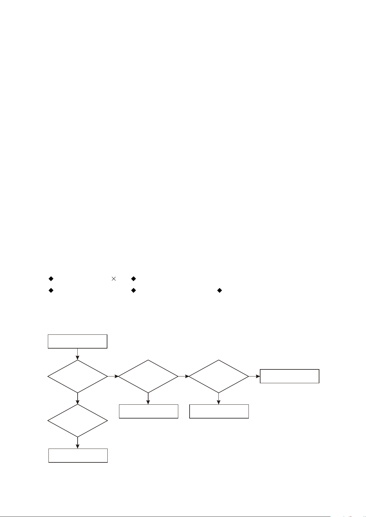
(1) Troubleshooting flow for “Left channel has no output” os shown as the following figure 3.1:
Left channel has no output
Check
whether pin 1
(or 3) of power amplifier
board Xp1 has wave form
after signal is
inputted
N
Change R13 and R14
Y
Check
whether the
anode wave form of
capacitor C1 (or C3)
is normal
N N
Change S3
Check
Y Y
whether the
anode wave form of
capacitor C12 (or C14)
is normal
Change U1
Change capacitor (C16)
N
Change input terminal
Figure 3.1 Troubleshooting flow for “ ”Left channel has no output
- 1 -

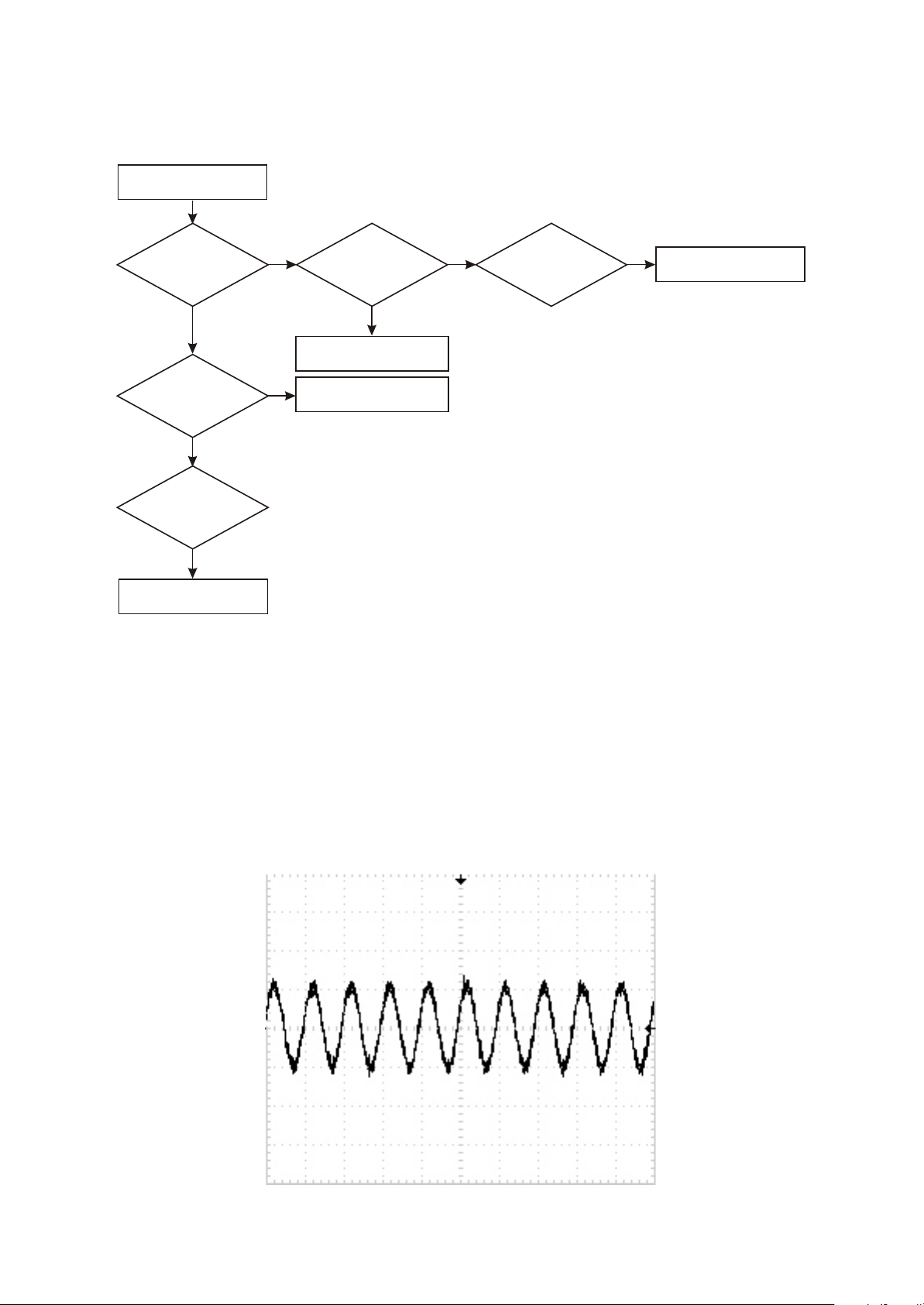
(2) Troubleshooting flow chart for “Power not on” is shown as the following figure 3.2:
Power not on
Check
whether protector
tube on power cord
has been burnt
down
Y
Check
whether protector
tube of power amplifier
board FL402 has been
burnt down
Y
Check
whether the
impedance of power
amplifier board power board
and grounding wire
is zero
Y
Change U1, transformer
and protector tube to solve
Check
N
N
whether protector
tube of power amplifier
board FL402 has been
burnt down
Change C17
and C11 to solve
Change transformer and
protector tube to solve
N
voltage of power amplifier
Y
Check
whether the power,
board is 22V
Figure 3.2 Troubleshooting flow chart for "Power not on”
N
Change U1 to solve
4. Signal waveform diagram
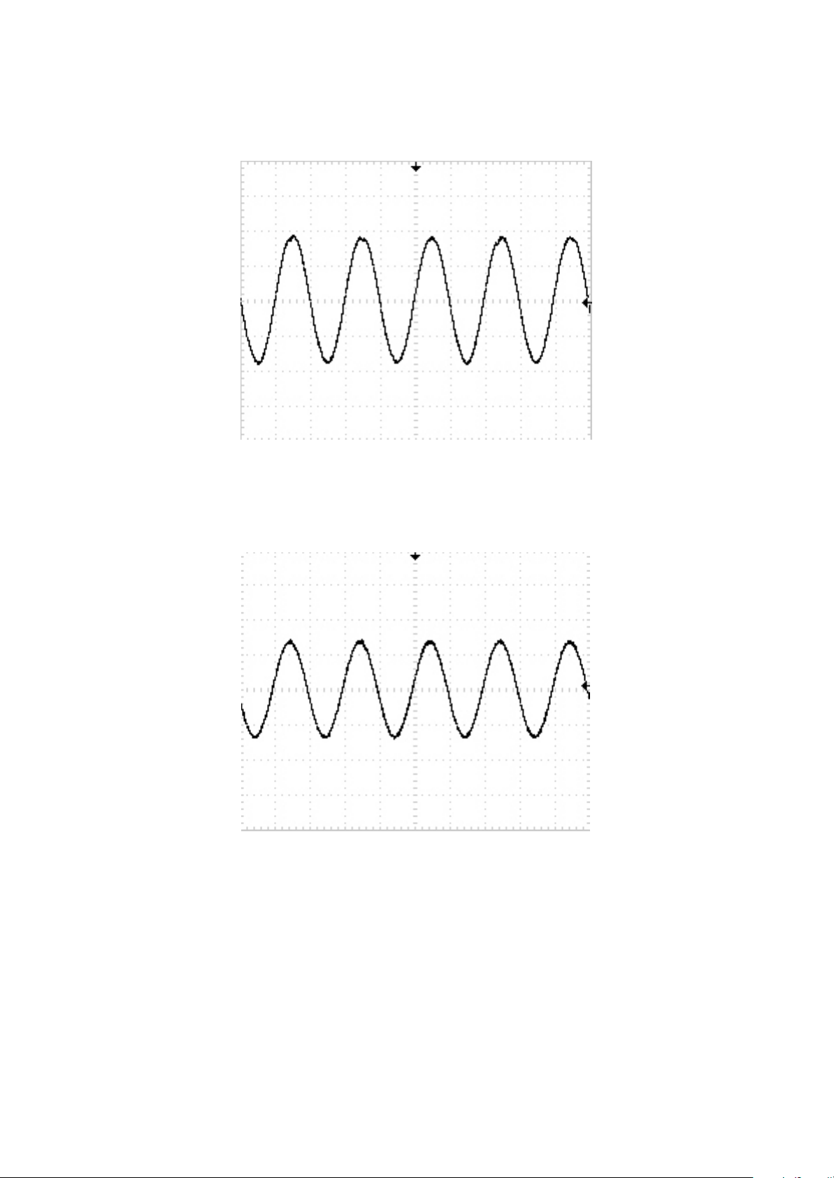
(1) Input waveform diagram of pin 2 of U1
- 2 -

(2) XS4 output signal waveform diagram
(3) External input signal waveform diagram
- 3 -
 Loading...