

Page 1

SERVICE MANUAL
DW9937S
Ver 0.0
Page 2

PREFACE
INDEX
FEATURES
FRONT PANEL&REAR PANEL
REMOTE CONTROL
........................................................................................................................
.................................................................................................................
BLOCK DIAGRAM
BLOCK DIAGRAM
.............................................................................................................
EXPLODED VIEW
EXPLODED VIEW
......................................................................................................................
PARTS SPECIFICATIONS
SST39VF16 0 ............................................................................................................................... 6
M13S128168A ............................................................................................................................
TSB41AB1
TVP5146
CS4360
CS5333 ......................................................................................................................................... 15
74HC/HCT14 ............................................................................................................................. 17
74ALVT16373 ...................................................................................................................... 18
MM1313 ............................................................................................................................................ 19-30
MAX4051 .......................................................................................................................................... 31-50
FSDM07652RB ................................................................................................................................ 51-70
LP2995
PQXXXEZ02Z .......................................................................................................................... 72
TUNER .............................................................................................................. 73
..................................................................................................................................
...................................................................................................................... 9
........................................................................................................................................ 13
................................................................................................................
........................................................................................................................
1
2
3
4
5
7
8
71
SCHEMA
TIC DIAGRAM&PCB SILKSCREEN
MAIN BOARD SCHEMATIC AND PCB LAYOUT
AV BOARD SCHEMATIC ..................................................................................................... 85-95
KEY BOARD SCHEMATIC .......................................................................................................
POWER BOARD SCHEMATIC ........................................................................................... 97
VCR MODLE 98-100
PARTSLIST
MAIN BOARD .............................................................................................................................. 101-102
MAIN PANEL BOARDKEY
POWER BOARD .............................................................................................................. 105-107
AV BOARD 108-110
............................................................................
.........................................................................................................................
......................................................................................................................
....................................................................................................................................
74-84
96
103-104
Page 3

1
Page 4

2
Page 5

3
Page 6

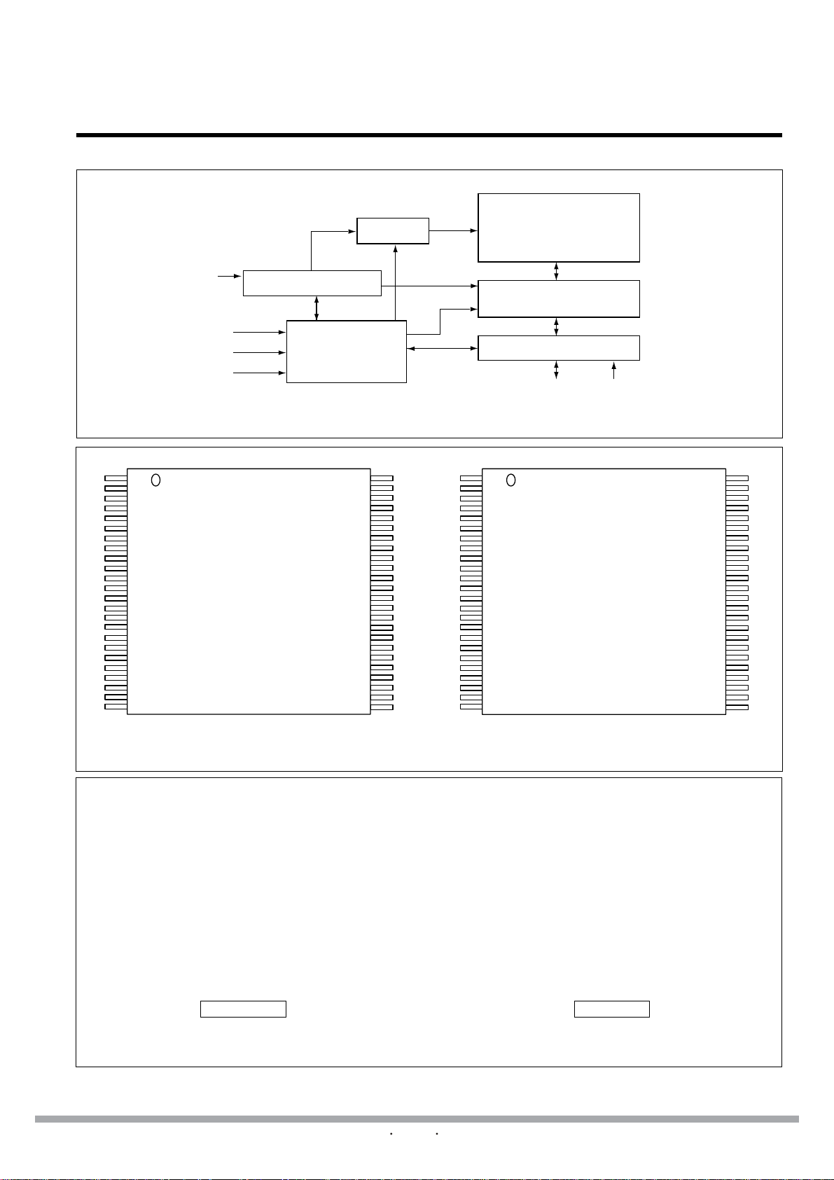
BLOCK DIAGRAM
POWER SUPPLY
Power board Video signal(s) Main pannel board
Audio signal(s)
Control signal(s)
wake up signal
Power on/off signal
VCR
VCR CVBS signal
HC4052
VCR L&R audio signals
MSP3415
CD4052
AV Channel
VMM1313
Switch
audio Signals outputs (except mixed L/R Audio) (except CVBS )
CVBS &mixed Audio inputs Video inputs Audio outputs Video outputs
key matrix
µPD16316
VFD-DISP
Video ADC
5146
DNM8602
Audio ADC
CS5333
CS4360
Audio
DVD L&R audio signals
DVD CVBS signal
Main board
4
AV board
Page 7

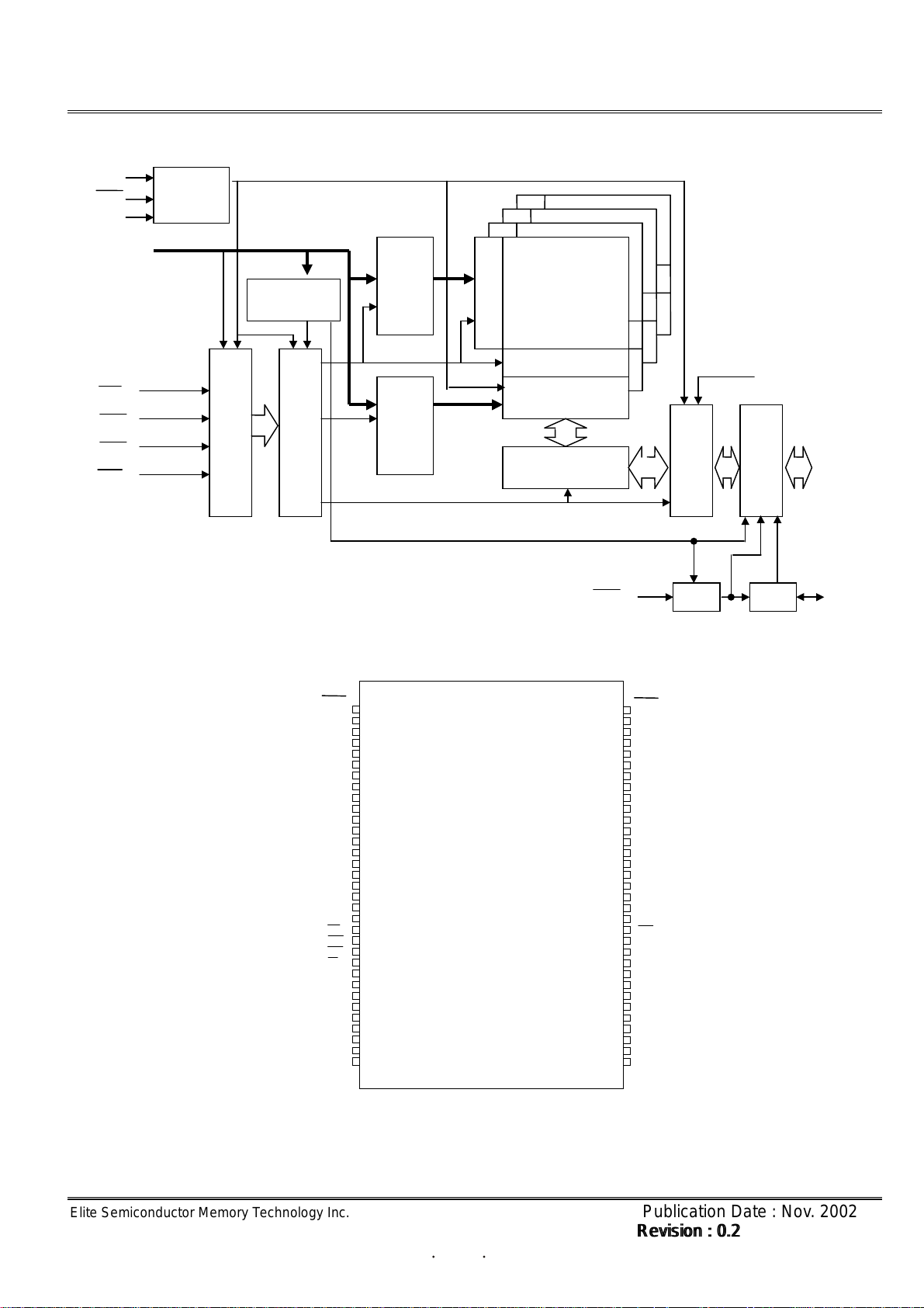
EXPLODED VIEW
55
Page 8
FUNCTIONAL BLOCK DIAGRAM
A19 - A
0
CE#
OE#
WE#
X-Decoder
Address Buffer & Latches
Control Logic
16 Megabit Multi-Purpose Flash
SST39VF160Q / SST39VF160
Advance Information
16,777,216 bit
EEPROM
Cell Array
Y-Decoder
I/O Buffers and Data Latches
DQ15 - DQ
V
0
DDQ
329 ILL B1.2
A15
A14
A13
A12
A11
A10
A19
WE#
A18
A17
1
2
3
4
5
6
A9
7
A8
8
9
NC
10
11
NC
12
NC
13
NC
14
NC
15
16
17
A7
18
A6
19
A5
20
A4
21
A3
22
A2
23
A1
24
Standard Pinout
T op Vie w
Die Up
SST39VF160Q
48
47
46
45
44
43
42
41
40
39
38
37
36
35
34
33
32
31
30
29
28
27
26
25
329 ILL F01.2
A16
V
V
DQ15
DQ7
DQ14
DQ6
DQ13
DQ5
DQ12
DQ4
V
DQ11
DQ3
DQ10
DQ2
DQ9
DQ1
DQ8
DQ0
OE#
V
CE#
A0
FIGURE 1: PIN ASSIGNMENTS FOR 48-PIN TSOP PACKAGES
123456
A
A3 A7 NC WE# A9 A13
B
A4 A17 NC NC A8 A12
C
A2 A6 A18 NC A10 A14
D
A1 A5 NC A19 A11 A15
E
A0 DQ0 DQ2 DQ5 DQ7 A16
F
CE# DQ8 DQ10 DQ12 DQ14 V
G
OE# DQ9 DQ11 V
H
V
DQ1 DQ3 DQ4 DQ6 V
SS
SST39VF160Q
DD
DQ13 DQ15
DDQ
SS
329 ILL F02.4
DDQ
SS
DD
SS
A15
A14
A13
A12
A11
A10
A19
WE#
A18
A17
NC
NC
NC
NC
NC
A9
A8
A7
A6
A5
A4
A3
A2
A1
1
2
3
4
5
6
7
8
9
10
11
12
13
14
15
16
17
18
19
20
21
22
23
24
Standard Pinout
T op Vie w
Die Up
SST39VF160
123456
A
A3 A7 NC WE# A9 A13
B
A4 A17 NC NC A8 A12
C
A2 A6 A18 NC A10 A14
D
A1 A5 NC A19 A11 A15
E
A0 DQ0 DQ2 DQ5 DQ7 A16
F
CE# DQ8 DQ10 DQ12 DQ14 NC
G
OE# DQ9 DQ11 V
H
V
DQ1 DQ3 DQ4 DQ6 V
SS
SST39VF160
DD
DQ13 DQ15
48
47
46
45
44
43
42
41
40
39
38
37
36
35
34
33
32
31
30
29
28
27
26
25
329 ILL F01a.0
SS
329 ILL F02a.0
A16
NC
V
SS
DQ15
DQ7
DQ14
DQ6
DQ13
DQ5
DQ12
DQ4
V
DD
DQ11
DQ3
DQ10
DQ2
DQ9
DQ1
DQ8
DQ0
OE#
V
SS
CE#
A0
FIGURE 2: PIN ASSIGNMENTS FOR 48-PIN TFBGA
6
Page 9
ESMT
M13S128168A
45
45
;(
45-45
2
2
66 PIN TSOP(II)
(400mil x 875mil)
(0.65 mm PIN PITCH)
Elite Semiconductor Memory Technology Inc.
7
Publication Date : Nov. 2002
Revision : 0.2
Revision : 0.2
Page 10

SLLS423D – JUNE 2000 – REVISED SEPTEMBER 2002
description (continued)
required for normal network operation regardless of the state of the PHY-LLC interface. When the interface is
in the reset or disabled state and LPS is again observed active, the PHY initializes the interface and returns it
to normal operation.
When the PHY-LLC interface is in the low-power disabled state, the TSB41AB1 automatically enters a
low-power mode if the port is inactive (disconnected, disabled, or suspended). In this low-power mode, the
TSB41AB1 disables its internal clock generators and also disables various voltage and current reference
circuits depending on the state of the port (some reference circuitry must remain active in order to detect new
cable connections, disconnections, or incoming TPBIAS, for example). The lowest power consumption (the
ultralow-power sleep mode) is attained when the port is either disconnected, or disabled with the port interrupt
enable bit cleared. The TSB41AB1 exits the low-power mode when the LPS input is asserted high or when a
port event occurs which requires that the TSB41AB1 become active in order to respond to the event or to notify
the LLC of the event (for example, incoming bias is detected on a suspended port, a disconnection is detected
on a suspended port, a new connection is detected on a nondisabled port, etc.). The SYSCLK output becomes
active (and the PHY-LLC interface is initialized and becomes operative) within 7.3 ms after LPS is asserted high
when the TSB41AB1 is in the low-power mode.
The PHY uses the C/LKON terminal to notify the LLC to power up and become active. When activated, the
C/LKON signal is a square wave of approximately 163-ns period. The PHY activates the C/LKON output when
the LLC is inactive and a wake-up event occurs. The LLC is considered inactive when either the LPS input is
inactive, as described above, or the LCtrl bit is cleared to 0. A wake-up event occurs when a link-on PHY packet
addressed to this node is received, or when a PHY interrupt occurs. The PHY deasserts the C/LKON output
when the LLC becomes active (both LPS active and the LCtrl bit set to 1). The PHY also deasserts the C/LKON
output when a bus reset occurs unless a PHY interrupt condition exists which would otherwise cause C/LKON
to be active.
PHP package terminal diagram
SYSCLK
CTL0
CTL1
D0
D1
D2
D3
D4
D5
D6
D7
PD
LREQ
DGND
DGND
47 46 45 44 4348 42 40 39 3841
1
2
3
4
5
6
7
8
9
10
11
12
14 15
LPS
DGND
C/LKON
16
13
PHP PACKAGE
(TOP VIEW)
DDDVDD
DV
XO
XI
TSB41AB1
17 18 19 20
ISO
PC1
PC2
PC0
DD
PLLGND
PLLV
FILTER1
22 23 24
21
DD
CPS
DV
TESTM
FILTER0
RESET
37
SE
SM
36
35
34
33
32
31
30
29
28
27
26
25
AGND
AV
DD
R1
R0
AGND
TPBIAS
TPA+
TPA–
TPB+
TPB–
AGND
AV
DD
8
POST OFFICE BOX 655303 • DALLAS, TEXAS 75265
Page 11

1.5 Functional Block Diagram
TVP5146
CVBS/
Pb/B/C
CVBS/
Y/G
CVBS/
Pr/R/C
CVBS/Y
VI_1_A
VI_1_B
VI_1_C
VI_2_A
VI_2_B
VI_2_C
VI_3_A
VI_3_B
VI_3_C
VI_4_A
Protection
Detector
Analog Front End
ADC1
ADC2
ADC3
ADC4
Sampling
Clock
Copy
M
U
X
Timing Processor
with Sync Detector
CVBS/Y/G
CVBS/Y
C
Y/G
Pb/B
Pr/R
VBI
Data
Slicer
Composite and S-Video Processor
Y/C
Separation
5-line
Adaptive
Comb
Gain/Offset
Y
C
Component
Luma
Processing
Chroma
Processing
Processor
Color
Space
Conversion
YCbCr
YCbCr
Host
Interface
Output
Formatter
Y[9:0]
C[9:0]
FSS
GPIO
XTAL1
XTAL2
PWDN
RESETB
AVID
DATACLK
FID
VS/VBLK
GLCO
HS/CS
DRDGDB
Figure 1–1. Functional Block Diagram
FSO
SCL
SDA
1–4
9
Page 12
1.6 Terminal Assignments
VI_1_A
CH1_A18GND
CH1_A18VDD
PLL_A18GND
PLL_A18VDD
XTAL2
XTAL1
PFP PACKAGE
(TOP VIEW)
VS/VBLK/GPIO
HS/CS/GPIO
FID/GPIO
C_0/GPIO
C_1/GPIO
DGND
DVDD
C_2/GPIO
C_3/GPIO
C_4/GPIO
C_5/GPIO
IOGND
IOVDD
TVP5146
VI_1_B
VI_1_C
CH1_A33GND
CH1_A33VDD
CH2_A33VDD
CH2_A33GND
VI_2_A
VI_2_B
VI_2_C
CH2_A18GND
CH2_A18VDD
A18VDD_REF
A18GND_REF
CH3_A18VDD
CH3_A18GND
VI_3_A
VI_3_B
VI_3_C
CH3_A33GND
CH3_A33VDD
79 78 77 76 7580 74 72 71 7073
1
2
3
4
5
6
7
8
9
10
11
12
13
14
15
16
17
18
19
20
22 23
24
VI_4_A
CH4_A33VDD
CH4_A33GND
25 26 27 28
SCL
AGND
DGND
CH4_A18VDD
CH4_A18GND
29
30 31 32 33
SDA
INTREQ
69 682167 66 65 64
34 35 36 37 38 39 40
DVDD
DGND
PWDN
RESETB
FSS/GPIO
63 62 61
IOVDD
AVID/GPIO
GLCO/I2CA
60
59
58
57
56
55
54
53
52
51
50
49
48
47
46
45
44
43
42
41
IOGND
DATACLK
C_6/GPIO/RED
C_7/GPIO/GREEN
C_8/GPIO/BLUE
C_9/GPIO/FSO
DGND
DVDD
Y_0
Y_1
Y_2
Y_3
Y_4
IOGND
IOVDD
Y_5
Y_6
Y_7
Y_8
Y_9
DGND
DVDD
Figure 1–2. Terminal Assignments Diagram
10
1–5
Page 13

TVP5146
1.7 Terminal Functions
Table 1–1. Terminal Functions
TERMINAL
NAME NUMBER
Analog Video
VI_1_A
VI_1_B
VI_1_C
VI_2_A
VI_2_B
VI_2_C
VI_3_A
VI_3_B
VI_3_C
VI_4_A
Clock Signals
DATACLK 40 O Line-locked data output clock.
XTAL1 74 I
XTAL2 75 O External clock reference output. Not connected if XTAL1 is driven by an external single-ended oscillator.
Digital Video
C[9:0]/
GPIO[9:0]
D_BLUE 58 I Digital BLUE input from overlay device
D_GREEN 59 I Digital GREEN input from overlay device
D_RED 60 I Digital RED input from overlay device
FSO 57 I Fast-switch overlay between digital RGB and any video
Y[9:0]
Miscellaneous Signals
FSS/GPIO 35 I/O
GLCO/I2CA 37 I/O
INTREQ 30 O Interrupt request
PWDN 33 I
RESETB 34 I Reset input, active low
80
1
2
7
8
9
16
17
18
23
57, 58,
59, 60,
63, 64,
65, 66,
69, 70
43, 44,
45, 46,
47, 50,
51, 52,
53, 54
I/O
VI_1_x: Analog video input for CVBS/Pb/B/C
VI_2_x: Analog video input for CVBS/Y/G
VI_3_x: Analog video input for CVBS/Pr/R/C
VI_4_A: Analog video input for CVBS/Y
I
Up to 10 composite, 4 S-video, and 2 composite or 3 component video inputs (or a combination thereof)
can be supported.
The inputs must be ac-coupled. The recommended coupling capacitor is 0.1 µF.
The possible input configurations are listed in the input select register at I2C subaddress 00h (see
Section 2.11.1).
External clock reference input. It may be connected to an external oscillator with a 1.8-V compatible clock
signal or a 14.31818-MHz crystal oscillator.
Digital video output of CbCr, C[9] is MSB and C[0] is LSB. Unused outputs can be left unconnected. Also,
these terminals can be programmable general-purpose I/O.
O
For the 8-bit mode, the two LSBs are ignored.
Digital video output of Y/YCbCr, Y[9] is MSB and Y[0] is LSB.
O
For the 8-bit mode, the two LSBs are ignored. Unused outputs can be left unconnected.
Fast-switch (blanking) input. Switching signal between the synchronous component video (YPbPr/RGB)
and the composite video input.
Programmable general-purpose I/O
Genlock control output (GLCO). Two Genlock data formats are available: TI format and real time control
(RTC) format.
During reset, this terminal is an input used to program the I2C address LSB.
Power down input:
1 = Power down
0 = Normal mode
DESCRIPTION
1–6
11
Page 14

Table 1–1. Terminal Functions (Continued)
TVP5146
TERMINAL
NAME NUMBER
Host Interface
SCL 28 I I2C clock input
SDA 29 I/O I2C data bus
Power Supplies
AGND 26 I Analog ground. Connect to analog ground.
A18GND_REF 13 I Analog 1.8-V return
A18VDD_REF 12 I Analog power for reference 1.8 V
CH1_A18GND
CH2_A18GND
CH3_A18GND
CH4_A18GND
CH1_A18VDD
CH2_A18VDD
CH3_A18VDD
CH4_A18VDD
CH1_A33GND
CH2_A33GND
CH3_A33GND
CH4_A33GND
CH1_A33VDD
CH2_A33VDD
CH3_A33VDD
CH4_A33VDD
DGND
DVDD
IOGND 39, 49, 62 I Digital power return
IOVDD 38, 48, 61 I Digital power. Connect to 3.3 V or less for reduced noise.
PLL_A18GND 77 I Analog power return
PLL_A18VDD 76 I Analog power. Connect to 1.8 V.
Sync Signals
HS/CS/GPIO 72 I/O
VS/VBLK/GPIO 73 I/O
FID/GPIO 71 I/O
AVID/GPIO 36 I/O
79
10
15
24
78
11
14
25
3
6
19
22
4
5
20
21
27, 32, 42,
56, 68
31, 41, 55,
67
I/O
I Analog 1.8-V return
I Analog power. Connect to 1.8 V.
I Analog 3.3-V return
I Analog power. Connect to 3.3 V.
I Digital return
I Digital power. Connect to 1.8 V.
Horizontal sync output or digital composite sync output
Programmable general-purpose I/O
Vertical sync output (for modes with dedicated VSYNC) or VBLK output
Programmable general-purpose I/O
Odd/even field indicator output. This terminal needs a pulldown resistor.
Programmable general-purpose I/O
Active video indicator output
Programmable general-purpose I/O
DESCRIPTION
121413151416151716
1–7
Page 15

Page 16

Page 17

Page 18

Page 19

Philips SemiconductorsProduct specification
Hex inverting Schmitt trigger 74HC/HCT14
PIN DESCRIPTION
PIN NO. SYMBOL NAME AND FUNCTION
1, 3, 5, 9, 11, 13 1A to 6A data inputs
2, 4, 6, 8, 10, 12 1Y to 6Y data outputs
7 GND ground (0 V)
14 V
CC
positive supply voltage
Fig.1 Pin configuration. Fig.2 Logic symbol. Fig.3 IEC logic symbol.
FUNCTION TABLE
INPUT OUTPUT
nA nY
L
H
Notes
1. H = HIGH voltage level
L = LOW voltage level
APPLICATIONS
• Wave and pulse shapers
• Astable multivibrators
• Monostable multivibrators
Fig.4 Functional diagram. Fig.5 Logic diagram
(one Schmitt trigger).
H
L
17
Page 20

Philips Semiconductors Product specification
74ALVT163732.5V/3.3V 16-bit transparent D-type latch (3-State)
LOGIC SYMBOL
47 46 44 43
1
1D0 1D1 1D2 1D3
1LE
1OE
1Q0 1Q1 1Q2651Q3
32
36 35 33 32
2D02D21 2D2 2D3
2LE
2OE
2Q0 2Q1 2Q2 2Q3
1413 1716
48
25
24
41 40 38 37
1D4 1D5 1D6 1D7
1Q4 1Q5 1Q6
30 29 27 26
2D4 2D5 2D6 2D7
2Q4 2Q5 2Q6 2Q7
98
2019 2322
1Q7
1211
SA00044
PIN DESCRIPTION
PIN NUMBER SYMBOL FUNCTION
47, 46, 44, 43, 41, 40, 38, 37,
36, 35, 33, 32, 30, 29, 27, 26
2, 3, 5, 6, 8, 9, 11, 12, 13,
14, 16, 17, 19, 20, 22, 23
1, 24 1OE, 2OE
48, 25 1LE, 2LE
4, 10, 15, 21, 28, 34, 39, 45 GND Ground (0V)
7, 18, 31, 42 V
1D0 – 1D7
2D0 – 2D7
1Q0 – 1Q7
2Q0 – 2Q7
CC
Data inputs
Data outputs
Output enable
inputs
(active-Low)
Enable inputs
(active-High)
Positive
supply voltage
LOGIC SYMBOL (IEEE/IEC)
1OE
1LE
2OE
2LE
1D1
1D2
1D3
1D4
1D5
1D6
1D7
1D8
2D1
2D2
2D3
2D4
2D5
2D6
2D7
2D8
1
48
24
25
47
46
44
43
41
40
38
37
36
35
33
32
30
29
27
26
1EN
C3
2EN
C4
3D
4D
PIN CONFIGURATION
1
1OE
2
1Q0
1Q1
3
GND
4
1Q2
5
6
1Q3
7
V
CC
8
1Q4
1Q5
9
GND
10
1Q6
11
1Q7
12
2Q0
13
2Q1
14
GND
15
16
2Q2
2Q3
17
18
V
CC
2Q4
19
20
2Q5
21
GND
22
2Q6
23
2Q7
24
2OE
1 ∇
2 ∇
48
47
46
45
44
43
42
41
40
39
38
37
36
35
34
33
32
31
30
29
28
27
26
25
SA00043
1LE
1D0
1D1
GND
1D2
1D3
V
CC
1D4
1D5
GND
1D6
1D7
2D0
2D1
GND
2D2
2D3
V
CC
2D4
2D5
GND
2D6
2D7
2LE
2
1Q1
3
1Q2
5
1Q3
6
1Q4
8
1Q5
9
1Q6
11
1Q7
12
1Q8
13
2Q1
14
2Q2
16
2Q3
17
2Q4
19
2Q5
20
2Q6
22
2Q7
23
2Q8
SW00010
18
Page 21

2
C BUS Control 5-Input 2-Output AV Switch MM1313
MITSUMI
I
I2C BUS Control 5-Input 2-Output AV Switch
Monolithic IC MM1313
Outline
This IC is a 5-input 2-output AV switch with I2C control, developed for use in televisions. Two outputs enable
it to support two screens or "picture-in-picture".
Features
1. Serial control by I2C bus.
2. 5-inputs, 2-outputs.
3. Video and audio system switches can be controlled independently.
4. 6dB amplifier built in to video system.
5. Built-in Y/C MIX circuit.
6. Slave address can be changed : 90H or 92H.
7. Audio muting possible by external pin.
8. Maintains high impedance even when I
9. Built-in 3 value discrimination function.
10.On-chip power ON reset function.
11.Two types of audio input impedance : 60kΩ and 30kΩ.
MM1313AD : 60kΩ MM1313BD : 30kΩ
12.Supports 2-screen or P-IN-P TV.
2
C BUS line (SDA, SCL) power supply is off.
Package
SDIP-42A (MM1313AD, MM1313BD)
Applications
1. Televisions
2. Other video equipment
19
Page 22

MITSUMI
Equivalent Block Diagram
2
C BUS Control 5-Input 2-Output AV Switch MM1313
I
20
Page 23

MITSUMI
Pin Function
2
C BUS Control 5-Input 2-Output AV Switch MM1313
I
Pin No.
Name
41 MTV-V
1 V1
7 V2
13 V3
27 STV
3 V1
9 V2
31 Y
5 V1-C
11 V2
29 C
42 MTV-L
2 V1
8 V2
14 V3
25 STV
40 MTV
4 V1
10 V2
16 V3
26 STV
-
-
-
-
-
IN1
-
IN1
-
-
-
-
-
-
Internal equivalent circuit diagram
Pin No.
Name
Internal equivalent circuit diagram
33 LOUT1
V
V
V
-
V
22 L
32 R
24 R
OUT2
OUT1
OUT2
Y
Y
36 BIAS
C
19 SCL
L
L
L
-
L
-
R
R
R
R
-
R
34 VOUT1
23 V
OUT2
37 YOUT1
39 C
OUT1
20 SDA
6 S1
12 S2
21 ADR
28 Mute
21
Page 24

MITSUMI
2
C BUS Control 5-Input 2-Output AV Switch MM1313
I
Absolute Maximum Ratings
Item Symbol Ratings Units
Storage temperature T
Operating temperature T
Power supply voltage V
Allowable power dissipation Pd 850 mW
Electrical Characteristics
Item Symbol
Operating power supply voltage
Current consumption I
V
OUT1 output
Voltage gain G
Frequency characteristics F
Differential gain DG
Differential phase DP
Input dynamic range D
V
OUT2 output
Voltage gain G
Frequency characteristics F
Differential gain DG
Differential phase DP
Input dynamic range D
YOUT1 output
Voltage gain
Frequency characteristics
Differential gain DGY TP2
Differential phase DPY TP2
(Ta=25°C, VCC=9V)
VCC 8910V
CC 38 VCC=9V, no signal, no load 40 52 mA
V1 TP1 Sine wave 1.0VP-P, 100kHz 5.5 6.0 6.5 dB
V1 TP1
V1 TP1
V1 TP1
V1 SG1~3 Maximum input for total higher 1.6 1.9 VP-P
V2 TP6 Sine wave 1.0VP-P, 100kHz 5.5 6.0 6.5 dB
V2 TP6
V2 TP6
V2 TP6
V2 SG1~3 Maximum input for total higher 1.6 1.9 VP-P
G
Y1 TP2
G
Y2 TP2
Y1 TP2
F
F
Y2 TP2
(Ta=25°C)
Measure
ment pin
STG
OPR
CC 12 V
-
40~+125
-
20~+75
Conditions (unless otherwise indicated,
Measurement Circuit Figure 1)
Sine wave 1.0V
Vn-V : Staircase 1V
P-P
, 10MHz/100kHz-1.0 0 1.0 dB
P-P
°
C
°
C
Min. Typ. Max. Units
APL=10~90%
Vn-Y : Staircase (luminance signal) 1V
Vn-C : Chroma signal 0.3V
P-P
P-P
-
30 3 %
APL=10~90%
Vn-V : Staircase 1V
P-P
APL=10~90%
Vn-Y : Staircase (luminance signal) 1V
Vn-C : Chroma signal 0.3V
P-P
P-P
-
3 0 3 deg
APL=10~90%
Sine wave 100kHz
harmonic distortion factor < 1.0%
Sine wave 1.0V
10MHz/100kHz
Vn-V : Staircase 1V
P-P
P-P
-
1.0 0 1.0 dB
APL=10~90%
Vn-Y : Staircase (luminance signal) 1V
Vn-C : Chroma signal 0.3V
P-P
P-P
-
30 3 %
APL=10~90%
Vn-V : Staircase 1V
P-P
APL=10~90%
Vn-Y : Staircase (luminance signal) 1V
Vn-C : Chroma signal 0.3V
P-P
P-P
-
3 0 3 deg
APL=10~90%
Sine wave 100kHz
harmonic distortion factor < 1.0%
Vn-Y : Sine wave 1.0V
YIN1 : Sine wave 2.0V
-
Y : Sine wave 1.0VP
Vn
10MHz/100kHz
Y
IN1 : Staircase 2.0VP-P
10MHz/100kHz
Vn-Y : Staircase 1V
APL=10~90%
Y
IN1: Staircase 2VP-P
P-P
, 100kHz
P-P
, 100kHz-0.5 0 0.5
-
P
P-P
5.5 6.0 6.5
-
1.0 0 1.0
-
1.0 0 1.0
-
30 3 %
APL=10~90%
Vn-Y : Staircase 1V
APL=10~90%
IN1 : Staircase 2VP-P
Y
P-P
-
3 0 3 deg
APL=10~90%
dB
dB
22
Page 25

MITSUMI
2
C BUS Control 5-Input 2-Output AV Switch MM1313
I
Item Symbol
D
Measure
ment pin
Y1 SG2 Maximum input for total higher 1.6 1.9
Input dynamic range
DY2 SG4 Maximum input for total higher 3.2 3.8
Output impedance Z
C
OUT1 output
Voltage gain
OYC150Ω
C1 TP3
G
G
C2 TP3
F
C1 TP3
Frequency characteristics
C2 TP3
F
Differential gain DG
Differential phase DP
C TP3
C TP3
D
C1 SG3 Maximum input for total higher 2.75 3.25
Input dynamic range
C2 SG5 Maximum input for total higher 5.5 6.5
D
Input impedance Z
Output impedance Z
OUT1 output
L
Voltage gain
Frequency characteristics F
Total higher harmonic distortion
Input dynamic range D
IC Vn
OC150Ω
G
L11 TP4 b7=0, Sine wave 2.5VP-P, 1kHz
G
L12 TP4 b7=1, Sine wave 2.5VP-P, 1kHz
L1 TP4 Sine wave 2.5VP-P, 1MHz/1kHz
1 TP4 Sine wave 2.5VP
THDL
L1 SG6 Maximum input for total higher 2.6 2.8 Vrms
Output offset voltage VOFFL133
Input impedance Z
Output impedance Z
L
OUT2 output
Voltage gain G
Frequency characteristics F
Total higher harmonic distortion
Input dynamic range D
IL1 426078kΩ
OL1 120 Ω
L2 TP7 Sine wave 2.5VP-P, 1kHz
L2 TP7 Sine wave 2.5VP-P, 1MHz/1kHz
THDL2 TP7 Sine wave 2.5VP
L2 SG6 Maximum input for total higher 2.6 2.8 Vrms
Output offset voltage VOFFL222
Output impedance Z
R
OUT1 output
Voltage gain
Frequency characteristics F
Total higher harmonic distortion
Input dynamic range D
OL2 120 Ω
R11 TP5 b7=0, Sine wave 2.5VP-P, 1kHz
G
G
R12 TP5 b7=1, Sine wave 2.5VP-P, 1kHz
R1 TP5 Sine wave 2.5VP-P, 1MHz/1kHz
R1 TP5 Sine wave 2.5VP-P, 1kHz 0.03 0.1 %
THD
R1 SG7 Maximum input for total higher 2.6 2.8 Vrms
Output offset voltage VOFFR132
Input impedance Z
Output impedance Z
IR1 426078kΩ
OR1 120 Ω
Conditions (unless otherwise indicated,
Measurement Circuit Figure 1)
Min. Typ. Max. Units
Vn-Y : Sine wave 100kHz
harmonic distortion factor < 1.0%
V
IN1 : Sine wave 100kHz
harmonic distortion factor < 1.0%
Vn-C : Sine wave 1.0V
CIN1 : Sine wave 2.0V
-
C : Sine wave 1.0VP
Vn
10MHz/100kHz
C
IN1 : Sine wave 2.0VP-P
10MHz/100kHz
IN1 : Staircase 2VP-P
C
APL=10~90%
C
IN1 : Staircase 2VP-P
APL=10~90%
P-P
, 100kHz
P-P
, 100kHz-0.5 0 0.5
-
P
5.5 6.0 6.5
-
1.0 0 1.0
-
1.0 0 1.0
-
30 3 %
-
3 0 3 deg
Vn-C : Sine wave 100kHz
harmonic distortion factor < 1.0%
CIN1: Sine wave 100kHz
harmonic distortion factor < 1.0%
-
C, CIN1 101520kΩ
-
6.5-6.0-5.5
-
0.5 0.0 0.5
-
3.0 0 1.0 dB
-
P, 1kHz 0.03 0.1 %
Sine wave 1kHz
harmonic distortion factor < 0.5%
L
OUT1 pin DC difference during
SW switching
-
0.5 0.0 0.5 dB
-
3.0 0 1.0 dB
-
P, 1kHz 0.03 0.1 %
Sine wave 1kHz
harmonic distortion factor < 0.5%
OUT2 pin DC difference during
L
SW switching
-
6.5-6.0-5.5
-
0.5 0.0 0.5
-
3.0 0 1.0 dB
Sine wave 1kHz
harmonic distortion factor < 0.5%
R
OUT1 pin DC difference during
SW switching
P-P
V
dB
dB
V
P-P
dB
0 ±15 mV
0 ±15 mV
dB
0 ±15 mV
23
Page 26

MITSUMI
SDA
SCL
t
BUF
P PS
tHD:STA tHD:DAT tHIGH tSU:DAT tSU:STA tSU:STD
tLOW
Sr
t
R tF
2
C BUS Control 5-Input 2-Output AV Switch MM1313
I
Item Symbol
Measure
ment pin
ROUT2 output
Voltage gain G
Frequency characteristics F
Total higher harmonic distortion
Input dynamic range D
R2 TP8 Sine wave 2.5VP-P, 1kHz
R2 TP8 Sine wave 2.5VP-P, 1MHz/1kHz
THDR2 TP8 Sine wave 2.5VP
R2 SG7 Maximum input for total higher 2.6 2.8 Vrms
Output offset voltage VOFFR224
Output impedance Z
OR2 120 Ω
Crosswalk
V
OUT 1 CTV1 TP1
OUT 2 CTV2 TP2
V
Y
OUT 1 CTY1 TP3
OUT 1 CTC1 TP6
C
L
OUT 1 CTL1 TP4
OUT 2 CTL2 TP5 Measurement Circuit Figure 2
L
R
OUT 1 CTR1 TP7 1kHz, 2.5VP-P
R
OUT 2 CTR2 TP8
Video I/O Pin Voltage
Input pin voltage V
VIP No signal, no load 4.6 4.9 5.2 V
VOP
V
Output pin voltage
V
SOP
Audio I/O Pin Voltage
Input pin voltage V
Output pin voltage V
AIP No signal, no load 4.0 4.3 4.6 V
AOP No signal, no load 3.9 4.2 4.5 V
Logic section (Refer to figure below)
Input voltage L V
Input voltage H V
Low level output voltage (SDA)
High level input current I
Low level input current I
Clock frequency f
Data transmission waiting time
SCL start hold time t
SCL low level hold time t
SCL high level hold time t
SCL start set-up time t
SDA data hold time t
SDA data set-up time t
SCL rise time t
SCL fall time t
SCL stop set-up time t
IL I
IH
VOL SDA for 3mA inflow 0.0 0.4 V
IH when SDA, SCL=4.5V impressed
IL when SDA, SCL=0.4V impressed
SCL 100 kHz
BUF 4.7 µS
t
HD;STA 4.0 µS
LOW 4.7 µS
HIGH 4.0 µS
SU;STA 4.7 µS
HD;DAT 200 nS
SD;DAT 250 nS
R 1000 nS
F 300 nS
SU;STO 4.0 µS
Conditions (unless otherwise indicated,
Measurement Circuit Figure 1)
-
P, 1kHz 0.03 0.1 %
Min. Typ. Max. Units
-
0.5 0.0 0.5 dB
-
3.0 0 1.0 dB
Sine wave 1kHz
harmonic distortion factor < 0.5%
R
OUT2 pin DC difference during
switching
Measurement Circuit Figure 2
for SG1 input : 4.43MHz, 1V
for SG2 input : 4.43MHz, 0.5V
VOUT1 pin, VOUT2 pin
No signal, no load
YOUT1 pin, COUT1 pin
No signal, no load
2
C logic low level discrimination value 0.0 1.5 V
2
I
Clogic high level discrimination value 3.0 5.0 V
P-P
P-P
4.1 4.4 4.7 V
3.3 3.6 3.9 V
-
-
0 ±15 mV
-
60-53 dB
-
60-53 dB
-
60-53 dB
-
60-53 dB
-
90-80 dB
-
90-80 dB
-
90-80 dB
-
90-80 dB
10 +10 µA
10 +10 µA
I2C BUS BUS Control Signal
24
Page 27

MITSUMI
Measurement Circuit
Measurement Circuit 1
2
C BUS Control 5-Input 2-Output AV Switch MM1313
I
25
Page 28

MITSUMI
Measurement Circuit 2 (Crosstalk measurement)
2
C BUS Control 5-Input 2-Output AV Switch MM1313
I
26
Page 29

2
SDA
SCL
S
123456 78A123 8A P
S:Start Condition
P:Stop Condition
A:Acknowledge
C BUS Control 5-Input 2-Output AV Switch MM1313
MITSUMI
I
I2C BUS
The I2C BUS is a BUS system developed by Philips for internal use in equipment. Data transmission is carried
out by the two SDA and SCL lines, in byte units, with the MSB first from start condition.
[Control Register]
The control register contains data sent from the master in order to determine the status of each switch.
S
Slave address
1001000/10
R/W
A
Control register 1
b7 b6 b5 b4 b3 b2 b1 b0
A
Control register 2
b7 b6 b5 b4 b3 b2 b1 b0
AP
Address byte Control data
The data format is set as shown in the figure above. The first 7 bits in the address byte are allocated to the
slave address, and the remaining 1 bit is allocated to the read/write bit. The read/write bit is set at 0 when
using as a control register.
The MM1313 slave address can be selected as 90H/92H depending on the status of the ADR pin. When ADR
pin is low it is 90H.
The relationship between the control register bits and switch control is as shown below.
b7 b6 b5 b4 b3 b2 b1 b0
Audio
S/Comp
Video-Select Audio-Select
Gain Select
The control register bits are reset to 0 when power is applied.
MM1313 control is carried out by the 3-byte structure of the 1 address byte and 2 control data bytes. The first
byte in the control data is control data for output 1, and the remaining 1 byte is control data for output 2.
All of the remaining data (fourth byte and after) are ignored.
Refer to the separate tables for details on switch control.
27
Page 30

2
Reset released
Reset status
Undefined
0.6V 4.3V 5.4V V
CC
C BUS Control 5-Input 2-Output AV Switch MM1313
MITSUMI
I
[Status Register]
The status register contains data for sending device status to the master.
S
A
Slave address R/W
Status register
NA P
1001000/11 b7b6b5b4b3b2b1b0
Address byte Status data
The data format is set as shown in the figure above. The first 7 bits in the address byte are allocated to the
slave address, and the remaining 1 bit is allocated to the read/write bit. The read/write bit is set at 1 when
using as a status register.
The MM1313 slave address can be selected as 91H/93H depending on the status of the ADR pin. When the
ADR pin is low it is 91H. However, the confirmation response after completion of the status register should be
non-acknowledge.
The status register output data as shown below.
b7 b6 b5 b4 b3 b2 b1 b0
P-ON S1 S1 S2 S2
RESET
OPEN SEL OPEN SEL
P-ON RESET : Returns 1 for power on reset. However once data read begins, 0 is returned next.
S1/S2 OPEN : Returns 0 when the S1/S2 pin is not open, and returns 1 when the S1/S2 pin is open
S1/S2 SEL : Returns 0 when the S1/S2 pin is not grounded, and returns 1 when the S1/S2 pin is grounded.
S1/S2 OPEN, SEL have 3-value discrimination, and the combinations are as shown below.
S1/S2 pin DC voltage S1/S2 OPEN S1/S2 SEL
0.8V or less 01
1.3V or more, 3.5V or less
00
4.5V or more 10
[Power On Reset]
Power on reset is built in to reset each control register to 0 when power is turned on.
Power on reset threshold has hysteresis as shown in the figure below. The IC power on reset status can be
discriminated by reading the status register P-ON RESET.
28
Page 31

MITSUMI
Switch Control Table
2
C BUS Control 5-Input 2-Output AV Switch MM1313
I
1. Video Output 1
b6 b5 b4 b3 VOUT1YOUT1COUT1
0000 Mute Mute Mute
0001MTV
0010 V1
0011 V2
0100 V3
0101 STV
10
01
11
1000 Mute Mute Mute
1001MTV
1010V1
1011V2
1100 V3
1101 STV
10
11
11
-
VYIN1CIN1
-
VYIN1CIN1
-
VYIN1CIN1
-
VYIN1CIN1
-
VYIN1CIN1
Mute Mute Mute
-
VYIN1CIN1
-
Y+C V1-YV1
-
Y+C V2-YV2
-
VYIN1CIN1
-
VYIN1CIN1
Mute Mute Mute
2. Video Output 2
b6 b5 b4 b3 VOUT2
0000 Mute
0001MTV
0010 V1
0011 V2
0100 V3
0101 STV
01
1000 Mute
1001MTV
-
C
-
C
1010V1
1011V2
1100 V3
1101 STV
11
10
11
10
11
-
-
-
Mute
-
Y+C
-
Y+C
-
Mute
-
V
V
V
V
-
V
-
V
V
-
V
3. Audio Output 1
Mute pin b2 b1 b0 LOUT1ROUT1
0 0 0 Mute Mute
001MTV
010 V1
1.5V or less 011 V2
(OPEN) 100 V3
101 STV
10
1
11
3.0V or more
---
-
L MTV-R
-
LV1
-
LV2
-
LV3
-
L STV-R
Mute Mute
Mute Mute
5. Audio Output 2
Mute pin b2 b1 b0 LOUT2ROUT2
0 0 0 Mute Mute
001MTV
010 V1
1.5V or less 011 V2
-
L MTV-R
-
LV1
-
LV2
4. Audio Output 1 Gain
Switching
b7 Output gain
0
-
R
-
R
-
R
-
R
-
R
1 0dB output
-
6dB output
(OPEN) 100 V3
101 STV
10
3.0V or more
1
11
---
Mute Mute
Mute Mute
-
LV3
-
L STV-R
29
-
R
Page 32

MITSUMI
Application Circuit
2
C BUS Control 5-Input 2-Output AV Switch MM1313
I
Notes
OUT is set at 4.4V and CIN at 4.9V
1. V
Please note that capacitance polarity may vary depending on comb filter bias.
2. Each audio output can be muted by making pin 19 high. Mute is off when it is open or low.
30
Page 33

19-0463; Rev 0; 1/96
Low-Voltage, CMOS Analog
Multiplexers/Switches
_______________General Description
The MAX4051/MAX4052/MAX4053 and MAX4051A/
MAX4052A/MAX4053A are low-voltage, CMOS analog
ICs configured as an 8-channel multiplexer (MAX4051/A),
two 4-channel multiplexers (MAX4052/A), and three single-pole/double-throw (SPDT) switches (MAX4053/A).
The A-suffix parts are fully characterized for on-resistance
match, on-resistance flatness, and low leakage.
These CMOS devices can operate continuously with
dual power supplies ranging from ±2.7V to ±8V or a
single supply between +2.7V and +16V. Each switch
can handle rail-to-rail analog signals. The off leakage
current is only 0.1nA at +25°C or 5nA at +85°C
(MAX4051A/MAX4052A/4053A).
All digital inputs have 0.8V to 2.4V logic thresholds,
ensuring TTL/CMOS-logic compatibility when using
±5V or a single +5V supply.
________________________Applications
Battery-Operated Equipment
Audio and Video Signal Routing
Low-Voltage Data-Acquisition Systems
Communications Circuits
____________________________Features
♦ Pin Compatible with Industry-Standard
74HC4051/74HC4052/74HC4053
♦ Guaranteed On-Resistance:
100Ω with ±5V Supplies
♦ Guaranteed Match Between Channels:
6Ω (MAX4051A–MAX4053A)
12Ω (MAX4051–MAX4053)
♦ Guaranteed Low Off Leakage Currents:
0.1nA at +25°C (MAX4051A–MAX4053A)
1nA at +25°C (MAX4051–MAX4053)
♦ Guaranteed Low On Leakage Currents:
0.1nA at +25°C (MAX4051A–MAX4053A)
1nA at +25°C (MAX4051–MAX4053)
♦ Single-Supply Operation from +2.0V to +16V
Dual-Supply Operation from ±2.7V to ±8V
♦ TTL/CMOS-Logic Compatible
♦ Low Distortion: < 0.04% (600Ω)
♦ Low Crosstalk: < -90dB (50Ω)
♦ High Off Isolation: < -90dB (50Ω)
______________Ordering Information
PART
MAX4051ACPE
MAX4051ACSE
MAX4051ACEE 0°C to +70°C
Ordering Information continued at end of data sheet.
TEMP. RANGE PIN-PACKAGE
0°C to +70°C
0°C to +70°C
16 Plastic DIP
16 Narrow SO
16 QSOP
MAX4051/A, MAX4052/A, MAX4053/A
___________________________________Pin Configurations/Functional Diagrams
TOP VIEW
MAX4053
1
2
3
4
5
6
7
8
DIP/SO/QSOP
V+
16
COMB
15
COMC
14
NOC
13
NCC
12
11
ADDC
10
ADDB
9
ADDA
NO1
NO3
COM
NO7
NO5
INH
V-
GND
MAX4051
1
2
3
4
5
6
7
LOGIC
8
DIP/SO/QSOP
MAX4052
NO0B
NO1B
COMB
NO3B
NO2B
INH
GND
1
2
3
4
5
6
V-
7
LOGIC
8
V+
16
NO2
15
NO4
14
NO0
13
NO6
12
11
ADDC
10
ADDB
9
ADDA
V+
16
NO1A
15
NO2A
14
COMA
13
NO0A
12
11
NO3A
10
ADDB
9
ADDA
NOB
NCB
NOA
COMA
NCA
INH
V-
GND
DIP/SO/QSOP
31
Page 34

Low-Voltage, CMOS Analog
Multiplexers/Switches
ABSOLUTE MAXIMUM RATINGS
Voltages Referenced to GND
V+ ........................................................................-0.3V to +17V
V-..........................................................................+0.3V to -17V
V+ to V-................................................................-0.3V to +17V
Voltage into Any Terminal (Note 1)..........(V- - 2V) to (V+ + 2V)
Continuous Current into Any Terminal..............................±30mA
Peak Current, NO or COM
(pulsed at 1ms, 10% duty cycle).................................±100mA
Note 1: Signals on any terminal exceeding V+ or V- are clamped by internal diodes. Limit forward-diode current to maximum
current rating.
Stresses beyond those listed under “Absolute Maximum Ratings” may cause permanent damage to the device. These are stress ratings only, and functional
operation of the device at these or any other conditions beyond those indicated in the operational sections of the specifications is not implied. Exposure to
absolute maximum rating conditions for extended periods may affect device reliability.
or 30mA (whichever occurs first)
Continuous Power Dissipation (T
Plastic DIP (derate 10.53mW/°C above +70°C)............842mW
Narrow SO (derate 8.70mW/°C above +70°C)..............696mW
QSOP (derate 8.00mW/°C above +70°C).....................640mW
CERDIP (derate 10.00mW/°C above +70°C)................800mW
Operating Temperature Ranges
MAX405_C_ E/MAX405_AC_E.............................0°C to +70°C
MAX405_E_ E/MAX405_AE_E...........................-40°C to +85°C
MAX405_MJE/MAX405_AMJE........................-55°C to +125°C
Storage Temperature Range.............................-65°C to +150°C
Lead Temperature (soldering, 10sec).............................+300°C
ELECTRICAL CHARACTERISTICS—Dual Supplies
(V+ = +4.5V to +5.5V, V- = -4.5V to -5.5V, TA= T
PARAMETER
ANALOG SWITCH
Analog Signal Range
COM–NO On-Resistance
COM–NO On-Resistance
Match Between Channels
(Note 3)
SYMBOL
, V
COM
R
ON
∆R
ON
NO
MAX4051/A, MAX4052/A, MAX4053/A
COM–NO On-Resistance
Flatness (Note 4)
NO Off Leakage Current
(Note 5)
R
FLAT(ON)
I
NO(OFF)
to T
MIN
V+ = 5V, V- = -5V, INO= 1mA,
V
= ±3V
COM
V+ = 5V, V- = -5V,
INO= 1mA,
V
= ±3V
COM
V+ = 5V, V- = -5V,
INO= 1mA,
V
= -3V, 0V, 3V
COM
V+ = 5.5V, V- = -5.5V,
VNO= 4.5V,
V
= -4.5V
COM
V+ = 5.5V, V- = -5.5V,
VNO= -4.5V,
V
= 4.5V
COM
, unless otherwise noted. Typical values are at TA= +25°C.)
MAX
CONDITIONS
MAX4051A,
MAX4052A,
MAX4053A
MAX4051,
MAX4052,
MAX4053
MAX4051A,
MAX4052A,
MAX4053A
MAX4051,
MAX4052,
MAX4053
MAX4051A,
MAX4052A,
MAX4053A
C, E, M
TA= +25°C
C, E, M
TA= +25°C 6
C, E, M 12
TA= +25°C
C, E, M 18
TA= +25°C
C, E, M 15
TA= +25°C
C, E -10 10
M
TA= +25°C -0.1 0.002 0.1
C, E
M
= +70°C)
A
MIN TYP MAX
(Note 2)
60 100
125
12
10
-1 0.002 1
-100 100
-5 5
-100 100
UNITS
VV- V+V
Ω
Ω
Ω
nA
32
Page 35

Low-Voltage, CMOS Analog
Multiplexers/Switches
ELECTRICAL CHARACTERISTICS—Dual Supplies (continued)
(V+ = +4.5V to +5.5V, V- = -4.5V to -5.5V, TA= T
SYMBOLPARAMETER
COM Off Leakage
Current (Note 5)
COM On Leakage
Current (Note 5)
I
COM(OFF)
I
COM(ON)
to T
MIN
V+ = 5.5V, V- = -5.5V,
VNO= 4.5V,
V
COM
V+ = 5.5V, V- = -5.5V,
VNO= -4.5V,
V
COM
V+ = 5.5V, V- = -5.5V,
V
COM
, unless otherwise noted. Typical values are at TA= +25°C.)
MAX
CONDITIONS
= -4.5V
= 4.5V
= VNO= ±4.5V
MAX4051A
MAX4051
MAX4052A,
MAX4053A
MAX4052,
MAX4053
MAX4051A
MAX4051
MAX4052A,
MAX4053A
MAX4052,
MAX4053
MAX4051A
MAX4051
MAX4052A,
MAX4053A
MAX4052,
MAX4053
TA= +25°C -0.1 0.002 0.1
C, E
M -100 100
TA= +25°C
C, E -10 10
M
TA= +25°C
C, E
M
TA= +25°C
C, E -5 5
M
TA= +25°C -0.1 0.002 0.1
C, E
M -100 100
TA= +25°C
C, E -10 10
M
TA= +25°C -0.1 0.002 0.1
C, E
M
TA= +25°C
C, E
M
TA= +25°C -0.1 0.002 0.1
C, E
M -100 100
TA= +25°C
C, E -10 10
M
TA= +25°C -0.1 0.002 0.1
C, E
M
TA= +25°C
C, E
M
MIN TYP MAX
(Note 2)
-5 5
-1 0.002 1
-100 100
-0.1 0.002 0.1
-2.5 2.5
-100 100
-1 0.002 1
-50 50
-5 5
-1 0.002 1
-100 100
-2.5 2.5
-50 50
-1 0.002 1
-5 5
-50 50
-5 5
-1 0.002 1
-100 100
-2.5 2.5
-50 50
-1 0.002 1
-5 5
-50 50
MAX4051/A, MAX4052/A, MAX4053/A
UNITS
nA
nA
33
Page 36

Low-Voltage, CMOS Analog
Multiplexers/Switches
ELECTRICAL CHARACTERISTICS—Dual Supplies (continued)
(V+ = +4.5V to +5.5V, V- = -4.5V to -5.5V, TA= T
SYMBOLPARAMETER
DIGITAL I/O
ADD, INH Input Logic
Threshold High
ADD, INH Input Logic
Threshold Low
ADD, INH Input Current
Logic High or Low
SWITCH DYNAMIC CHARACTERISTICS
Turn-On Time (Note 6) Figure 3
Turn-Off Time (Note 6) Figure 3
Transition Time Figure 2
Break-Before-Make Delay Figure 4
NO Off Capacitance VNO= GND, f = 1MHz, Figure 7
COM Off Capacitance
Switch On Capacitance
Off Isolation
Channel-to-Channel
Crosstalk
POWER SUPPLY
IH
IL
IL
t
ON
t
OFF
TRANS
OPEN
NO(OFF)
COM(OFF)
(ON)
ISO
CT
MAX4051/A, MAX4052/A, MAX4053/A
I+V+ Supply Current INH = ADD = 0V or V+
I-V- Supply Current INH = ADD = 0V or V+
Note 2: The algebraic convention is used in this data sheet; the most negative value is shown in the minimum column.
Note 3: ∆R
Note 4: Flatness is defined as the difference between the maximum and minimum value of on-resistance as measured over the
Note 5: Leakage parameters are 100% tested at maximum-rated hot operating temperature, and guaranteed by correlation at
Note 6: Guaranteed by design, not production tested.
= R
ON
specified analog signal ranges; i.e., V
= +25°C.
T
A
ON(MAX)
- R
ON(MIN)
.
to T
MIN
V
, V
ADD
CL= 1nF, RS= 0Ω, VNO= 0V,
Figure 5
V
= GND, f = 1MHz, Figure 7
COM
V
= V
COM
Figure 7
CL= 15pF, RL= 50Ω, f = 100kHz,
VNO= 1V
CL= 15pF, RL= 50Ω, f = 100kHz,
VNO= 1V
= 3V to 0V and 0V to -3V.
NO
, unless otherwise noted. Typical values are at TA= +25°C.)
MAX
CONDITIONS
= V+, 0V
INH
= GND, f = 1MHz,
NO
, Figure 6
RMS
, Figure 6
RMS
MIN TYP MAX
(Note 2)
C, E, M V2.4V
C, E, M V0.8V
C, E, M µA-1 0.03 1IIH, I
TA= +25°C
C, E, M
TA= +25°C
C, E, M
TA= +25°C
TA= +25°C
TA= +25°C
TA= +25°C pF2C
TA= +25°C pF2C
TA= +25°C pF8C
TA= +25°C dB<-90V
TA= +25°C dB<-90V
C, E, M V±2.7 ±8V+, V-Power-Supply Range
TA= +25°C
C, E, M
TA= +25°C -1 0.1 1
C, E, M
50 175
40 150
210t
-1 0.1 1
-10
225
200
10
UNITS
ns
ns
ns75 250t
ns
pC210QCharge Injection (Note 6)
µA
µA
34
Page 37

Low-Voltage, CMOS Analog
Multiplexers/Switches
ELECTRICAL CHARACTERISTICS—Single +5V Supply
(V+ = +4.5V to +5.5V, V- = 0V, TA= T
SYMBOLPARAMETER
ANALOG SWITCH
Analog Signal Range
COM–NO On-Resistance
NO Off Leakage Current
(Note 5)
COM Off Leakage
Current (Note 5)
COM On Leakage
Current (Note 5)
DIGITAL I/O
ADD, INH Input Logic
Threshold High
ADD, INH Input Logic
Threshold Low
ADD, INH Input Current
Logic High or Low
POWER SUPPLY
COM
I
NO(OFF)
I
COM(OFF)
I
COM(ON)
, V
R
ON
V
IH
V
IL
IH, IIL
to T
MIN
NO
, unless otherwise noted. Typical values are at TA= +25°C.)
MAX
V+ = 5V, INO= 1mA,
V
= 3.5V
COM
V+ = 5.5V, VNO= 4.5V,
V
= 0V
COM
V+ = 5.5V, VNO= 0V,
V
= 4.5V
COM
V+ = 5.5V, VNO= 4.5V,
V
= 0V
COM
V+ = 5.5V, VNO= 0V,
V
= 4.5V or 0V
COM
V+ = 5.5V,
V
= VNO= 4.5V
COM
ADD, VINH
INH = ADD = 0V or V+ µAI+V+ Supply Current
CONDITIONS
MAX4051/A
MAX4052/A,
MAX4053/A
MAX4051/A
MAX4052/A,
MAX4053/A
MAX4051/A
MAX4052/A,
MAX4053/A
= V+, 0V µAI
MIN TYP MAX
(Note 2)
C, E, M
TA= +25°C
C, E, M
TA= +25°C -1 0.002 1
C, E
M
TA= +25°C
C, E
M
TA= +25°C -1 0.002 1
C, E
M -100 100
TA= +25°C
C, E -5 5
M
TA= +25°C -1 0.002 1
C, E
M -100 100
TA= +25°C
C, E -5 5
M
TA= +25°C
C, E -10 10
M
TA= +25°C -1 0.002 1
C, E
M
C, E, M 2.4
C, E, M 0.8
C, E, M -1 0.03 1V
TA= +25°C -1 1
C, E, M 10
V- V+V
125 225
280
-10 10
-100 100
-1 0.002 1
-10 10
-100 100
-10 10
-1 0.002 1
-50 50
-10 10
-1 0.002 1
-50 50
-1 0.002 1
-100 100
-10 10
-100 100
MAX4051/A, MAX4052/A, MAX4053/A
UNITS
V
Ω
nA
nA
nA
V
V
35
Page 38

Low-Voltage, CMOS Analog
Multiplexers/Switches
ELECTRICAL CHARACTERISTICS—Single +5V Supply (continued)
(V+ = +4.5V to +5.5V, V- = 0V, TA= T
SYMBOLPARAMETER
DIGITAL I/OSWITCH DYNAMIC CHARACTERISTICS
Turn-On Time (Note 6) Figure 3
Turn-Off Time (Note 6)
Break-Before-Make Delay Figure 4
Off Isolation
Channel-to-Channel
Crosstalk
Note 2: The algebraic convention is used in this data sheet; the most negative value is shown in the minimum column.
Note 3: ∆R
Note 4: Flatness is defined as the difference between the maximum and minimum value of on-resistance as measured over the
Note 5: Leakage parameters are 100% tested at maximum-rated hot operating temperature, and guaranteed by correlation at
Note 6: Guaranteed by design, not production tested.
= R
ON
specified analog signal ranges; i.e., V
= +25°C.
T
A
ON(MAX)
- R
ON(MIN)
t
ON
t
OFF
OPEN
ISO
CT
to T
MIN
.
, unless otherwise noted. Typical values are at TA= +25°C.)
MAX
Figure 3
CL= 1nF, RS= 0Ω, VNO= 0V,
Figure 5
CL= 15pF, RL= 50Ω, f = 100kHz,
VNO= 1V
CL= 15pF, RL= 50Ω, f = 100kHz,
VNO= 1V
NO
, Figure 6
RMS
, Figure 6
RMS
= 3V to 0V and 0V to -3V.
CONDITIONS
TA= +25°C
C, E, M
TA= +25°C
C, E, M
TA= +25°C
TA= +25°C
TA= +25°C dB<-90V
TA= +25°C dB<-90V
MIN TYP MAX
(Note 2)
90 200
275
60 125
175
UNITS
ns
ns
ns30t
pC210QCharge Injection (Note 6)
MAX4051/A, MAX4052/A, MAX4053/A
36
Page 39

Low-Voltage, CMOS Analog
Multiplexers/Switches
ELECTRICAL CHARACTERISTICS—Single +3V Supply
(V+ = +3.0V to +3.6V, V- = 0V, TA= T
SYMBOLPARAMETER
ANALOG SWITCH
Analog Signal Range
COM–NO On-Resistance
NO Off Leakage Current
(Note 5)
COM Off Leakage
Current (Note 5)
COM On Leakage
Current (Note 5)
DIGITAL I/O
ADD, INH Input Logic
Threshold High
ADD, INH Input Logic
Threshold Low
ADD, INH Input Current
Logic High or Low
POWER SUPPLY
COM
I
NO(OFF)
I
COM(OFF)
I
COM(ON)
to T
MIN
, V
NO
R
ON
V
IH
V
IL
IH, IIL
I+ INH = ADD = 0V or V+V+ Supply Current µA
, unless otherwise noted. Typical values are at TA= +25°C.)
MAX
CONDITIONS
INO= 1mA, V+ = 3V,
V
= 1.5V
COM
V+ = 3.6V, VNO= 3V,
V
= 0V
COM
V+ = 3.6V, VNO= 0V,
V
= 3V
COM
MAX4051/A
V+ = 3.6V, VNO= 3V,
V
= 0V
COM
V+ = 3.6V, VNO= 0V,
V
= 3V
COM
V+ = 3.6V,
V
= VNO= 3V
COM
V
ADD, VINH
= V+, 0V
MAX4052/A,
MAX4053/A
MAX4051/A
MAX4052/A,
MAX4053/A
MAX4051/A
MAX4052/A,
MAX4053/A
MIN TYP MAX
(Note 2)
C, E, M
TA= +25°C
C, E, M
TA= +25°C
C, E
M
TA= +25°C
C, E
M
TA= +25°C -1 0.002 1
C, E
M -100 100
TA= +25°C
C, E -5 5
M
TA= +25°C -1 0.002 1
C, E
M -100 100
TA= +25°C
C, E -5 5
M
TA= +25°C
C, E -10 10
M
TA= +25°C
C, E
M
C, E, M 2.4
C, E, M 0.8
C, E, M -1 0.03 1I
TA= +25°C -1 1
C, E, M 10
V- V+V
250 525
700
-1 0.002 1
-10 10
-100 100
-1 0.002 1
-10 10
-100 100
-10 10
-1 0.002 1
-50 50
-10 10
-1 0.002 1
-50 50
-1 0.002 1
-100 100
-1 0.002 1
-10 10
-100 100
MAX4051/A, MAX4052/A, MAX4053/A
UNITS
V
Ω
nA
nA
nA
nA
V
V
µA
nA
37
Page 40

Low-Voltage, CMOS Analog
Multiplexers/Switches
ELECTRICAL CHARACTERISTICS—Single +3V Supply (continued)
(V+ = +3.0V to +3.6V, V- = 0V, TA= T
SYMBOLPARAMETER
DIGITAL I/OSWITCH DYNAMIC CHARACTERISTICS
Turn-On Time (Note 6) Figure 3
Turn-Off Time (Note 6)
Break-Before-Make Delay Figure 4
Off Isolation
Channel-to-Channel
Crosstalk
Note 2: The algebraic convention is used in this data sheet; the most negative value is shown in the minimum column.
Note 3: ∆R
Note 4: Flatness is defined as the difference between the maximum and minimum value of on-resistance as measured over the
Note 5: Leakage parameters are 100% tested at maximum-rated hot operating temperature, and guaranteed by correlation at
Note 6: Guaranteed by design, not production tested.
= R
ON
specified analog signal ranges; i.e., V
= +25°C.
T
A
ON(MAX)
- R
ON(MIN)
t
ON
t
OFF
OPEN
ISO
CT
to T
MIN
.
, unless otherwise noted. Typical values are at TA= +25°C.)
MAX
Figure 3
CL= 1nF, RS= 0Ω, VNO= 0V,
Figure 5
CL= 15pF, RL= 50Ω, f = 100kHz,
VNO= 1V
CL= 15pF, RL= 50Ω, f = 100kHz,
VNO= 1V
NO
, Figure 6
RMS
, Figure 6
RMS
= 3V to 0V and 0V to -3V.
CONDITIONS
TA= +25°C
C, E, M
TA= +25°C
C, E, M
TA= +25°C
TA= +25°C
TA= +25°C dB<-90V
TA= +25°C dB<-90V
MIN TYP MAX
(Note 2)
180 600
700
100 300
400
UNITS
ns
ns
ns90t
pC110QCharge Injection (Note 6)
MAX4051/A, MAX4052/A, MAX4053/A
38
Page 41

Low-Voltage, CMOS Analog
Multiplexers/Switches
__________________________________________Typical Operating Characteristics
(V+ = +5V, V- = -5V, GND = 0V, TA= +25°C, unless otherwise noted.)
ON-RESISTANCE vs. V
(DUAL SUPPLIES)
110
100
90
80
(Ω)
70
ON
R
60
50
40
30
-5 -3 1
ON-RESISTANCE vs. V
AND TEMPERATURE
180
160
140
120
(Ω)
ON
100
R
80
60
40
02
(SINGLE SUPPLY)
V+ = 5V
V- = 0V
153
5
Qj (pC)
COM
V± = ±3V
V± = ±5V
-1 3
V
(V)
COM
TA = +125°C
T
= +25°C
A
V
(V)
COM
COM
TA = +85°C
TA = -55°C
4
5-4 0-2 2 4
CHARGE INJECTION vs. V
V+ = 5V
V- = 0V
110
100
MAX4051/2/3-TOC1
90
80
(Ω)
70
ON
R
60
50
40
30
1000
MAX4051/2/3-TOC4
100
OFF-LEAKAGE (pA)
0.1
COM
ON-RESISTANCE vs. V
AND TEMPERATURE
(DUAL SUPPLIES)
V+ = 5V
V- = -5V
TA = +125°C
TA = +85°C
TA = +25°C
TA = -55°C
-5 -3 1
V+ = 5.5V
V- = -5.5V
10
1
-50 12525-25 0 7550 100
OFF-LEAKAGE vs.
TEMPERATURE (°C)
MAX4051/2/3-TOC7
-1 3
V
TEMPERATURE
COM
(V)
COM
10
1
I+, I- (nA)
MAX4051/2/3-TOC2
5-4 0-2 2 4
10,000
MAX4051/2/3-TOC5
SUPPLY CURRENT vs.
TEMPERATURE
V+ = 5V
V- = -5V
= VA = 0V, 5V
V
EN
ON-RESISTANCE vs. V
300
275
250
225
200
(Ω)
175
ON
R
150
125
100
75
50
02
1000
100
10
ON-LEAKAGE (pA)
1
0.1
-50 12525-25 0 7550 100
(SINGLE SUPPLY)
V- = 0V
153
V
COM
ON-LEAKAGE vs.
TEMPERATURE
V+ = 5.5V
V- = -5.5V
TEMPERATURE (°C)
I+
I-
V+ = 3V
(V)
MAX4051/2/3-TOC8
V+ = 5V
COM
4
MAX4051/A, MAX4052/A, MAX4053/A
MAX4051/2/3-TOC3
MAX4051/2/3-TOC6
V+ = 5V
V- = -5V
-5
-5 -3 1
-1 305-4 0-2 2 4
V
(V)
COM
39
0.1
-50 12525-25 0 7550 100
TEMPERATURE (°C)
Page 42

Low-Voltage, CMOS Analog
Multiplexers/Switches
____________________________Typical Operating Characteristics (continued)
(V+ = +5V, V- = -5V, GND = 0V, TA= +25°C, unless otherwise noted.)
FREQUENCY RESPONSE
0
-10
-20
INSERTION LOSS
-30
-40
-50
LOSS (dB)
-60
-70
-80
-90
0.01 0.1 1 10 100 300
OFF ISOLATION
ON PHASE
50Ω IN/OUT
FREQUENCY (MHz)
5
0
MAX4051/2/3-09
-5
-10
-15
-20
-25
-30
-35
-40
PHASE (DEGREES)
_____________________________________________________________Pin Descriptions
PIN
NO0B–NO3B—
NO0A–NO3A—
NAME
NO0–NO7—
COMB15
ADDA9
ADDB10
ADDC11
COMA4
COMC14
COM—
NOB1
NCB2
NOA3
NCA5
INH
GND8
NCC12
NOC13
Analog Switch Inputs 0–7—
Analog Switch Common—3
Analog Switch “B” Inputs 0–31, 2, 5, 4—
Analog Switch “B” Common3—
Analog Switch “B” Normally Open Input——
Analog Switch “B” Normally Closed Input——
Analog Switch “A” Normally Open Input——
Analog Switch “A” Normally Closed Input——
Digital Inhibit Input. Normally connect to GND. Can be driven
to logic high to set all switches off.
V-7
Negative Analog Supply Voltage Input. Connect to GND for
single-supply operation.
Ground. Connect to digital ground. (Analog signals have no
ground reference; they are limited to V+ and V-.)
Digital Address “A” Input99
Digital Address “B” Input1010
Digital Address “C” Input—11
Analog Switch “A” Inputs 0–312, 15, 14, 11—
Analog Switch “A” Common13—
Analog Switch “C” Normally Closed Input——
Analog Switch “C” Normally Open Input——
Analog Switch “C” Common——
Positive Analog and Digital Supply Voltage Input1616 V+16
MAX4051/
MAX4051A
MAX4052/
MAX4052A
MAX4053/
MAX4053A
13, 1, 15, 2,
14, 5, 12, 4
MAX4051/A, MAX4052/A, MAX4053/A
66
6
77
88
Note: NO, NC, and COM pins are identical and interchangeable. Any may be considered an input or output; signals pass equally
well in both directions.
TOTAL HARMONIC DISTORTION
100
V± = ±5V
600Ω IN AND OUT
10
1
THD (%)
0.1
0.01
10 100 1k 10k
vs. FREQUENCY
FREQUENCY (Hz)
FUNCTION
MAX4051/2/3-10
40
Page 43

Low-Voltage, CMOS Analog
Multiplexers/Switches
Table 1. Truth Table/Switch Programming
ON SWITCHESADDRESS BITS
INH
X = Don’t care * ADDC not present on MAX4052.
Note: NO and COM pins are identical and interchangeable. Either may be considered an input or output; signals pass equally well
in either direction.
ADDC*
X1
00
00
00
00
10
10
10
10
ADDB ADDA
X X All switches open All switches open All switches open
0 0 COM–NO0
0 1 COM–NO1
1 0 COM–NO2
1 1 COM–NO3
0 0 COM–NO4
0 1 COM–NO5
1 0 COM–NO6
1 1 COM–NO7
MAX4051/
MAX4051A
MAX4052/
MAX4052A
COMB–NO0B,
COMC–NO0C
COMB–NO1B,
COMC–NO1C
COMB–NO2B,
COMC–NO2C
COMB–NO3B,
COMC–NO3C
COMB–NO0B,
COMC–NO0C
COMB–NO1B,
COMC–NO1C
COMB–NO2B,
COMC–NO2C
COMB–NO3B,
COMC–NO3C
MAX4053/
MAX4053A
COMA–NCA,
COMB–NCB,
COMC–NCC
COMA–NOA,
COMB–NCB,
COMC–NCC
COMA–NCA,
COMB–NOB,
COMC–NCC
COMA–NOA,
COMB–NOB,
COMC–NCC
COMA–NCA,
COMB–NCB,
COMC–NOC
COMA–NOA,
COMB–NCB,
COMC–NOC
COMA–NCA,
COMB–NOB,
COMC–NOC
COMA–NOA,
COMB–NOB,
COMC–NOC
MAX4051/A, MAX4052/A, MAX4053/A
__________Applications Information
Power-Supply Considerations
Overview
The MAX4051/MAX4052/MAX4053 and MAX4051A/
MAX4052A/MAX4053A construction is typical of most
CMOS analog switches. They have three supply pins:
V+, V-, and GND. V+ and V- are used to drive the internal CMOS switches and set the limits of the analog voltage on any switch. Reverse ESD-protection diodes are
internally connected between each analog signal pin
and both V+ and V-. If any analog signal exceeds V+ or
V-, one of these diodes will conduct. During normal
operation, these (and other) reverse-biased ESD diodes
leak, forming the only current drawn from V+ or V-.
41
Virtually all the analog leakage current comes from the
ESD diodes. Although the ESD diodes on a given signal
pin are identical, and therefore fairly well balanced,
they are reverse biased differently. Each is biased by
either V+ or V- and the analog signal. This means their
leakages will vary as the signal varies. The
difference
the two diode leakages to the V+ and V- pins constitutes the analog signal path leakage current. All analog
leakage current flows between each pin and one of the
supply terminals, not to the other switch terminal. This is
why both sides of a given switch can show leakage currents of either the same or opposite polarity.
There is no connection between the analog signal
paths and GND.
in
Page 44

Low-Voltage, CMOS Analog
Multiplexers/Switches
V+ and GND power the internal logic and logic-level
translators, and set both the input and output logic limits. The logic-level translators convert the logic levels
into switched V+ and V- signals to drive the gates of
the analog signals. This drive signal is the only connection between the logic supplies (and signals) and the
analog supplies. V+ and V- have ESD-protection
diodes to GND.
The logic-level thresholds are TTL/CMOS compatible
when V+ is +5V. As V+ rises, the threshold increases
slightly, so when V+ reaches +12V, the threshold is
about 3.1V; above the TTL-guaranteed high-level minimum of 2.8V, but still compatible with CMOS outputs.
COM NO
Bipolar Supplies
These devices operate with bipolar supplies between
±3.0V and ±8V. The V+ and V- supplies need not be
symmetrical, but their sum cannot exceed the absolute
maximum rating of +17V.
EXTERNAL BLOCKING DIODE
Single Supply
These devices operate from a single supply between
+3V and +16V when V- is connected to GND. All of the
bipolar precautions must be observed. At room temperature, they actually “work” with a single supply at near
or below +1.7V, although as supply voltage decreases,
switch on-resistance and switching times become very
high.
Figure 1. Overvoltage Protection Using External Blocking
Diodes
Overvoltage Protection
Proper power-supply sequencing is recommended for
all CMOS devices. Do not exceed the absolute maximum ratings, because stresses beyond the listed ratings can cause permanent damage to the devices.
Always sequence V+ on first, then V-, followed by the
logic inputs (NO) and by COM. If power-supply
MAX4051/A, MAX4052/A, MAX4053/A
sequencing is not possible, add two small signal diodes
(D1, D2) in series with the supply pins for overvoltage
protection (Figure 1).
Adding diodes reduces the analog signal range to one
diode drop below V+ and one diode drop above V-, but
does not affect the devices’ low switch resistance and
low leakage characteristics. Device operation is
unchanged, and the difference between V+ and Vshould not exceed 17V. These protection diodes are
not recommended when using a single supply if signal
levels must extend to ground.
In 50Ω systems, signal response is reasonably flat up
to 50MHz (see
Above 20MHz, the on response has several minor
peaks which are highly layout dependent. The problem
is not turning the switch on, but turning it off. The offstate switch acts like a capacitor, and passes higher
frequencies with less attenuation. At 10MHz, off isolation is about -45dB in 50Ω systems, becoming worse
(approximately 20dB per decade) as frequency
increases. Higher circuit impedances also make off isolation worse. Adjacent channel attenuation is about 3dB
above that of a bare IC socket, and is entirely due to
capacitive coupling.
V+
*
*
V-
High-Frequency Performance
Typical Operating Characteristics
V+
D1EXTERNAL BLOCKING DIODE
MAX4051/A
MAX4052/A
MAX4053/A
*
*
D2
V-
* INTERNAL PROTECTION DIODES
).
42
Page 45

Low-Voltage, CMOS Analog
Multiplexers/Switches
______________________________________________Test Circuits/Timing Diagrams
V
50Ω
V
50Ω
ADD
ADD
ADDC
ADDB
ADDA
INH
ADDC
ADDB
INH
V+
V+
MAX4051/A
GND
V+
V+
MAX4052/A
GND
NO0
NO1–NO6
NO7
COM
V-
V-
NO0
NO1–NO2
NO3
COM
V-
V-
300Ω
300Ω
V+
V-
V
OUT
35pF
V+
V-
V
OUT
35pF
V+
V
ADD
0V
V
NO0
0V
V
OUT
V
NO7
t
TRANS
V+
V
ADD
0V
V
NO0
0V
V
OUT
V
NO3
t
TRANS
50%
50%
90%
90%
90%
90%
t
TRANS
t
TRANS
MAX4051/A, MAX4052/A, MAX4053/A
V+
V
ADD
50Ω
V- = 0V FOR SINGLE-SUPPLY OPERATION.
REPEAT TEST FOR EACH SECTION.
ADD
INH
V+
MAX4053/A
GND
Figure 2. Address Transition Time
V+
V
NO
V-
NC
V+
COM
V-
300Ω
V-
35pF
V
OUT
ADD
0V
V
NC
0V
V
OUT
V
NO
t
TRANS
50%
90%
90%
t
TRANS
43
Page 46

Low-Voltage, CMOS Analog
Multiplexers/Switches
V+
V+
GND
GND
GND
V+
V+
V+
V+
NO0
NO1–NO7
COM
V-
V-
NO0
NO1–NO3
COM
V-
V-
COM
V-
V-
V+
V
OUT
300Ω
300Ω
NO
NC
300Ω
35pF
V+
V
OUT
35pF
V+
V-
V
OUT
35pF
ADDC
ADDB
ADDA
V
INH
50Ω
V
INH
50Ω
MAX4051/A, MAX4052/A, MAX4053/A
V
INH
50Ω
MAX4051/A
INH
ADDC
ADDB
MAX4052/A
INH
ADD
MAX4053/A
INH
V+
V
INH
0V
V
NO0
V
OUT
0V
V+
V
INH
0V
V
NO0
V
OUT
0V
V+
V
INH
0V
V
NO_
V
OUT
0V
50%
t
ON
50%
t
ON
50%
t
ON
90%
90%
90%
90%
90%
90%
t
OFF
t
OFF
t
OFF
V- = 0V FOR SINGLE-SUPPLY OPERATION.
REPEAT TEST FOR EACH SECTION.
Figure 3. Enable Switching Time
44
Page 47

V+
V
ADD
50Ω
V
ADD
50Ω
V- = 0V FOR SINGLE-SUPPLY OPERATION.
REPEAT TEST FOR EACH SECTION.
ADDC
ADDB
ADDA
INH
ADD
INH
V+
MAX4051/A
GND
V+
V+
MAX4053/A
GND
NO0–N07
COM
V-
V-
NO, NC
COM
V-
V-
300Ω
300Ω
Low-Voltage, CMOS Analog
Multiplexers/Switches
MAX4051/A, MAX4052/A, MAX4053/A
V+
V
V+
V
OUT
35pF
V+
V
OUT
35pF
ADD
50Ω
V+
V
ADD
0V
V
NO_
V
OUT
0V
ADDC
ADDB
INH
V+
MAX4052/A
GND
50%
t
OPEN
NO0–NO3
COM
V-
V-
80%
300Ω
t
R
t
F
< 20ns
< 20ns
V+
V
OUT
35pF
Figure 4. Break-Before-Make Interval
V+
V+
CHANNEL
SELECT
ADDC
ADDB
MAX4051/A
ADDA
V
INH
50Ω
MAX4052/A
MAX4053/A
INH
GND
V- = 0V FOR SINGLE-SUPPLY OPERATION.
REPEAT TEST FOR EACH SECTION.
Figure 5. Charge Injection
V+
V
NO
COM
V-
V-
VNO = 0V
V
OUT
CL = 1000pF
INH
0V
V
OUT
∆ V
IS THE MEASURED VOLTAGE DUE TO CHARGE
OUT
TRANSFER ERROR Q WHEN THE CHANNEL TURNS OFF.
Q = ∆ V
X C
OUT
L
∆ V
OUT
45
Page 48

Low-Voltage, CMOS Analog
Multiplexers/Switches
V+
V+
CHANNEL
SELECT
ADDC
ADDB
ADDA
MAX4051/A
MAX4052/A
MAX4053/A
INH
GND
V-
10nF
V-
MEASUREMENTS ARE STANDARDIZED AGAINST SHORT AT SOCKET TERMINALS.
OFF ISOLATION IS MEASURED BETWEEN COM AND "OFF" NO TERMINAL ON EACH SWITCH.
ON LOSS IS MEASURED BETWEEN COM AND "ON" NO TERMINAL ON EACH SWITCH.
CROSSTALK (MAX4052 AND MAX4053) IS MEASURED FROM ONE CHANNEL (A, B, C) TO ALL OTHER CHANNELS.
SIGNAL DIRECTION THROUGH SWITCH IS REVERSED; WORST VALUES ARE RECORDED.
Figure 6. Off Isolation, On Loss, and Crosstalk
10nF
COM
V
NO
IN
V
OUT
MEAS.
NETWORK
ANALYZER
50Ω
50Ω 50Ω
50Ω
REF.
OFF ISOLATION = 20log
ON LOSS = 20log
CROSSTALK = 20log
V
OUT
V
IN
V
OUT
V
IN
V
OUT
V
IN
V+
MAX4051/A, MAX4052/A, MAX4053/A
CHANNEL
SELECT
ADDC
ADDB
ADDA
V+
MAX4051/A
NO
NO
MAX4052/A
MAX4053/A
INH
GND
COM
V-
V-
Figure 7. NO/COM Capacitance
46
1MHz
CAPACITANCE
ANALYZER
Page 49

Low-Voltage, CMOS Analog
Multiplexers/Switches
___________________________________________Ordering Information (continued)
PART
MAX4051AEPE
MAX4051AEEE
MAX4051CPE
MAX4051CSE
MAX4051C/D
MAX4051EEE
MAX4052ACPE
MAX4052ACEE
MAX4052AEEE
MAX4052CPE
MAX4052CEE
MAX4052ESE
-40°C to +85°C
-40°C to +85°CMAX4051AESE
-55°C to +125°CMAX4051AMJE
0°C to +70°C
0°C to +70°CMAX4051CEE
-40°C to +85°CMAX4051EPE
-55°C to +125°CMAX4051MJE
0°C to +70°CMAX4052ACSE
-40°C to +85°CMAX4052AEPE
-55°C to +125°CMAX4052AMJE
0°C to +70°CMAX4052CSE
0°C to +70°CMAX4052C/D
-40°C to +85°CMAX4052EEE
PIN-PACKAGETEMP. RANGE
16 Plastic DIP
16 Narrow SO
16 QSOP-40°C to +85°C
16 CERDIP**
16 Plastic DIP0°C to +70°C
16 Narrow SO
16 QSOP
Dice*0°C to +70°C
16 Plastic DIP
16 Narrow SO-40°C to +85°CMAX4051ESE
16 QSOP-40°C to +85°C
16 CERDIP**
16 Plastic DIP0°C to +70°C
16 Narrow SO
16 QSOP0°C to +70°C
16 Plastic DIP
16 Narrow SO-40°C to +85°CMAX4052AESE
16 QSOP-40°C to +85°C
16 CERDIP**
16 Plastic DIP0°C to +70°C
16 Narrow SO
16 QSOP0°C to +70°C
Dice*
16 Plastic DIP-40°C to +85°CMAX4052EPE
16 Narrow SO-40°C to +85°C
16 QSOP
16 CERDIP**-55°C to +125°CMAX4052MJE
PIN-PACKAGETEMP. RANGEPART
MAX4053ACPE
0°C to +70°CMAX4053ACSE
MAX4053ACEE
-40°C to +85°CMAX4053AEPE
MAX4053AEEE
-55°C to +125°CMAX4053AMJE
MAX4053CPE
0°C to +70°CMAX4053CSE
MAX4053CEE
0°C to +70°CMAX4053C/D
MAX4053ESE
-40°C to +85°CMAX4053EEE
16 Plastic DIP0°C to +70°C
16 Narrow SO
16 QSOP0°C to +70°C
16 Plastic DIP
16 Narrow SO-40°C to +85°CMAX4053AESE
16 QSOP-40°C to +85°C
16 CERDIP**
16 Plastic DIP0°C to +70°C
16 Narrow SO
16 QSOP0°C to +70°C
Dice*
16 Plastic DIP-40°C to +85°CMAX4053EPE
16 Narrow SO-40°C to +85°C
16 QSOP
16 CERDIP**-55°C to +125°CMAX4053MJE
* Contact factory for dice specifications.
** Contact factory for availability.
___________________Chip Topography
MAX4051/A
COM
N.C.
NO6
NO7
NO5
INH
NO4 V+
NO2
NO1
N.C.
NO0
0.108"
(2.74mm)
NO3
ADDA
MAX4051/A, MAX4052/A, MAX4053/A
N.C. = NO CONNECT
TRANSISTOR COUNT: 161
SUBSTRATE CONNECTED TO V+.
47
V-
ADDC
GND
0.080"
(2.03mm)
ADDB
Page 50

Low-Voltage, CMOS Analog
Multiplexers/Switches
_____________________________________________Chip Topographies (continued)
MAX4052/A
MAX4053/A
COMC
NO3C
N.C.
NO1C
INH
NO2C
N.C. = NO CONNECT
NO0C V+
V-
N.C.
GND
0.080"
(2.03mm)
ADDC
TRANSISTOR COUNT: 161
SUBSTRATE CONNECTED TO V+.
NO2B
NO1B
COMB
NO0B
(2.74mm)
NO3B
ADDB
0.108"
NCB
N.C.
NOC
COMC
NCC
INH
N.C. = NO CONNECT
TRANSISTOR COUNT: 161
SUBSTRATE CONNECTED TO V+.
V-
NOB V+
GND
0.080"
(2.03mm)
MAX4051/A, MAX4052/A, MAX4053/A
ADDC
COMB
N.C.
COMA
NOA
0.108"
(2.74mm)
NCA
ADDA
ADDB
48
Page 51

Low-Voltage, CMOS Analog
Multiplexers/Switches
________________________________________________________Package Information
INCHES MILLIMETERS
0°-8°
PKG.
P
P
P
P
P
N
DIM
A
A1
A2
A3
B
B1
C
D1
E
E1
e
eA
eB
L
DIM
PINS
D
D
D
D
D
D
DIM
A
A1
B
C
E
e
H
L
MAX
MIN
–
0.015
0.125
0.055
0.016
0.045
0.008
0.005
0.300
0.240
0.100
0.300
–
0.115
INCHES MILLIMETERS
MIN
8
0.348
14
0.735
16
0.745
18
0.885
20
1.015
24
1.14
INCHES MILLIMETERS
MIN
0.053
0.004
0.014
0.007
0.150
0.228
0.016
0.200
–
0.175
0.080
0.022
0.065
0.012
0.080
0.325
0.310
–
–
0.400
0.150
MAX
0.069
0.010
0.019
0.010
0.157
0.244
0.050
MAX
0.390
0.765
0.765
0.915
1.045
1.265
MIN
0.38
3.18
1.40
0.41
1.14
0.20
0.13
7.62
6.10
2.54
7.62
2.92
18.67
18.92
22.48
25.78
28.96
MIN
1.35
0.10
0.35
0.19
3.80
5.80
0.40
–
–
MIN
8.84
1.270.050
MAX
5.08
–
4.45
2.03
0.56
1.65
0.30
2.03
8.26
7.87
–
–
10.16
3.81
MAX
9.91
19.43
19.43
23.24
26.54
32.13
21-0043A
MAX
1.75
0.25
0.49
0.25
4.00
6.20
1.27
E
D
E1
A3
A2
A
L
A1
e
B1
B
0° - 15°
C
eA
eB
D1
Plastic DIP
PLASTIC
DUAL-IN-LINE
PACKAGE
(0.300 in.)
D
A
0.101mm
e
A1
B
0.004in.
C
L
MAX4051/A, MAX4052/A, MAX4053/A
Narrow SO
HE
SMALL-OUTLINE
PACKAGE
(0.150 in.)
DIM
D
D
D
MIN
MAX
MIN
8
0.189
0.337
0.386
0.197
0.344
0.394
14
16
4.80
8.55
9.80
MAX
5.00
8.75
10.00
21-0041A
INCHES MILLIMETERS
PINS
49
Page 52

Low-Voltage, CMOS Analog
Multiplexers/Switches
_________________________________________Packaging Information (continued)
INCHES MILLIMETERS
DIM
D
A
e
A1
B
S
H
E
A
A1
A2
B
C
D
E
e
H
h
L
N
S
α
MIN
0.061
0.004
0.055
0.008
0.0075
0.150
0.230
0.010
0.016
0°
MAX
MIN
0.068
0.061
0.012
0.157
0.244
0.016
0.035
8°
1.55
0.127
1.40
0.20
0.19
3.81
0.635 BSC0.25 BSC
5.84
0.25
0.41
0°
0.0098
0.0098
SEE VARIATIONS
SEE VARIATIONS
SEE VARIATIONS
MAX
1.73
0.25
1.55
0.31
0.25
3.99
6.20
0.41
0.89
8°
DIM
D
S
D
S
D
S
D
S
h x 45°
N
A2
α
SMALL-OUTLINE
E
C
L
INCHES MILLIMETERS
PINS
MIN
0.189
0.0020
0.337
0.0500
0.337
0.0250
0.386
0.0250
MAX
0.196
0.0070
0.344
0.0550
0.344
0.0300
0.393
0.0300
16
16
20
20
24
24
28
28
QSOP
QUARTER
PACKAGE
MIN
4.80
0.05
8.56
1.27
8.56
0.64
9.80
0.64
MAX
4.98
0.18
8.74
1.40
8.74
0.76
9.98
0.76
21-0055A
MAX4051/A, MAX4052/A, MAX4053/A
50
Page 53

FSDM07652RB
www.fairchildsemi.com
Green Mode Fairchild Power Switch (FPS
Features
• Internal Avalanche Rugged Sense FET
• Advanced Burst-Mode operation consumes under 1 W at
240VA C & 0.5W load
• Precision Fixed Operating Frequency (66kHz)
• Internal Start-up Circuit
• Improved Pulse by Pulse Current Limiting
• Over Voltage Protection (OVP)
• Over Load Protection (OLP)
• Internal Thermal Shutdown Function (TSD)
• Auto-Restart Mode
• Under Voltage Lock Out (UVLO) with hysteresis
• Low Operating Current (2.5mA)
•
Built-in Soft Start
Application
• SMPS for LCD monitor and STB
• Adaptor
Description
The FSDM07652RB is an integrated Pulse Width Modulator
(PWM) and Sense FET specifically designed for high performance offline Switch Mode Power Supplies (SMPS) with
minimal external components. This device is an integrated
high voltage power switching regulator which co mbine an
avalanche rugged Sense FET with a current mode PWM control blo ck. The PWM controller includes integrated fixed frequency oscillator, under voltage lockout, leading edge blanking
(LEB), optimized gate driver, internal soft start, te mperature
compensated precise current sources for a loop compensation
and self protection circuitry. Compared with discrete MOSFET and PWM controller solution, it can reduce total cost,
component count, size and weight simultaneously increasing efficiency, productivity, and system reliability. This d evice i s a
basic platform well suited for cost effective designs of flyback converters.
PRODUCT
FSDM0565RB 60W 70W 50W 60W
FSDM07652RB 70W 80W 60W 70W
Notes:
1. Typical continuous power in a non-ventilated enclosed
adapter measured at 50°C ambient.
2. Maximum practical continuous power in an open frame
design at 50°C ambient.
3. 230 VAC or 100/115 VAC with doubler.
Typical Circuit
AC
IN
OUTPUT POWER TABLE
230VAC ±15%
Adapt-
(1)
er
Open
Frame
Table 1. Maximum Output Power
Drain
Vstr
PWM
Vfb Vcc
Figure 1. Typical Flyback Application
Source
TM
(3)
(2)
)
85-265VAC
Adapt-
(1)
er
Open
Frame
DC
OUT
(2)
51
Page 54

FSDM07652RB
Internal Block Diagram
N.C
FB
5
4
0.5/0.7V
I
delay
V
SD
Vcc
Vovp
TSD
+
-
Vcc Vref
Soft start
Vcc
3 1
8V/12V
I
FB
2.5R
Vcc good
OSC
PWM
R
I
start
Vstr
Vref
SQQ
R
6
Internal
Bias
Gate
driver
Drain
LEB
2
GND
Vcc good
SQQ
R
V
CL
Figure 2. Functional Block Diagram of FSDM07652RB
52
Page 55

Pin Definitions
Pin Number Pin Nam e Pin Function Description
1Drain
2 GND This pin is the control ground and the Sense FET source.
3Vcc
4Vfb
5N.C-
6Vstr
This pin is the high voltage power Sense FET drain. It is designed to drive the
transformer directly.
This pin is the positive supply voltage input. During start up, the power is supplied by an internal high voltage current source that is connected to the Vstr pin.
When Vcc reaches 12V , the internal high voltage current source is disabled and
the power is supplied from the auxiliary transformer winding.
This pin is internally connected to the inverting input of the PWM comparator.
The collector of an opto-coupler is typically tied to this pin. For stable operation,
a capacitor should be placed between this pin and GND. If the voltage of this pin
reaches 6.0V, the over load protection is activated resulting in shutdown of the
TM
FPS
.
This pin is connected directly to the high voltage DC link. At startup, the internal
high voltage current source supplies internal bias and charges the external capacitor that is connected to the Vcc pin. Once Vcc reaches 12V , the internal current source is disabled.
FSDM07652RB
Pin Configuration
TO-220F-6L
6.Vstr
5.N.C.
4.Vfb
3.Vcc
2.GND
1.Drain
Figure 3. Pin Configuration (Top View)
53
Page 56

FSDM07652RB
Absolute Maximum Ratings
(Ta=25°C, unless otherwise specified)
Parameter Symbol Value Unit
Vstr Max Voltage V
Pulsed Drain current (Tc=25
Continuous Drain Current(Tc=25
Continuous Drain Current(Tc=100
Single pulsed avalanche energy
Single pulsed avalanche current
°C)
(1)
°C)
°C)
(2)
(3)
Supply voltage V
Input voltage range V
Total power dissipation(Tc=25
°C)
Operating junction temperature T
Operating ambient temperature T
Storage temperature range T
Notes:
1. Repetitive rating: Pulse width limited by maximum junction temperature
2. L=14mH, starting Tj=25°C
3. L=13uH, starting Tj=25°C
STR
I
DM
I
D
E
AS
I
AS
CC
FB
PD(Watt H/S) 62 W
j
A
STG
650 V
28 A
7A
4.5 A
370 mJ
-A
19 V
-0.3 to V
CC
+150 °C
-25 to +85 °C
-55 to +150 °C
DC
V
Thermal Impedance
Parameter Symbol Value Unit
Junction-to-Ambient Thermal
Junction-to-Case Thermal
Notes:
1. Free standing with no heat-sink under natural convection.
2. Infinite cooling condition - Refer to the SEMI G30-88.
(1)
θ
JA
(2)
θ
JC
46.40 °C/W
2.49 °C/W
54
Page 57

Electrical Characteristics
(Ta = 25°C unless otherwise specified)
Parameter Symbol Condition Min. Typ. Max. Unit
Sense FET SECTION
Drain source breakdown voltage BV
Zero gate voltage drain current I
Static drain source on resistance
Output capacitance C
(1)
DSS
R
DS(ON)
OSS
DSS
V
= 0V, ID = 250µA 650 - - V
GS
V
= 650V, V
DS
= 520V
V
DS
V
= 0V, TC = 125°C
GS
V
= 10V, ID = 2.5A - 1.4 1.6
GS
V
= 0V, V
GS
f = 1MHz
= 0V - - 50 µA
GS
- - 200 µA
= 25V,
DS
- 100 - pF
FSDM07652RB
Ω
Turn on delay time T
D(ON)
Rise time T
Turn off delay time T
D(OFF)
Fall time T
CONTROL SECTION
Initial frequency F
Voltage stability F
Temperature stability
(2)
STABLE
∆F
Maximum duty cycle D
Minimum duty cycle D
Start threshold voltage V
Stop threshold voltage V
START
STOP
Feedback source current I
Soft-start time T
Leading Edge Blanking time T
BURST MODE SECTION
R
F
OSC
OSC
MAX
MIN
FB
S
LEB
VDD= 325V, ID= 5A
(MOSFET switching
time is essentially
independent of
operating temperature)
-22-
-60ns
-115-
-65-
VFB = 3V 60 66 72 kHz
13V ≤ Vcc ≤ 18V 0 1 3 %
-25°C ≤ Ta ≤ 85°C0±5±10%
-758085%
---0%
VFB=GND 11 12 13 V
VFB=GND 789V
VFB=GND 0.7 0.9 1.1 mA
Vfb=3 - 10 15 ms
- - 250 - ns
Burst Mode Voltages
(2)
V
V
PROTECTION SECTION
Peak current limit
(4)
I
OVER
Over voltage protection V
Thermal shutdown temperature
(2)
Shutdown feedback voltage V
Shutdown delay current I
DELAY
BURH
BURL
OVP
T
SD
SD
Vcc=14V - 0.7 - V
Vcc=14V - 0.5 - V
VFB=5V, VCC=14V 2.2 2.5 2.8 A
-181920V
130 145 160 °C
VFB ≥ 5.5V 5.5 6.0 6.5 V
VFB=5V 2.8 3.5 4.2 µA
55
Page 58

FSDM07652RB
TOTAL DEVICE SECTION
I
OP
Operating supply current
Notes:
1. Pulse test : Pulse width ≤ 300µS, duty ≤ 2%
2. These parameters, although guaranteed at the design, are not tested in mass production.
3. These parameters, although guaranteed, are tested only in EDS(wafer test) process.
4. These parameters indicate the inductor current.
5. This parameter is the current flowing into the control IC.
(5)
OP(MIN)
I
OP(MAX)
VFB=GND, VCC=14V
VFB=GND, VCC=10V
VFB=GND, VCC=18V
-2.55mAI
56
Page 59

FSDM07652RB
Comparison Between FS6M07652RTC and FSDM07652RB
Function FS6M07652RTC FSDM07652RB FSDM07652RB Advantages
Soft-Start Adjustable soft-start
time using an
external capacitor
Burst Mode Operation • Built into controller
• Output voltage
drops to around
half
Internal soft-start with
typically 10ms (fixed)
• Built into controller
• Output voltage fixed
• Gradually increasing current limit
during soft-start further reduces peak
current and voltage component
stresses
• Eliminates external components used
for soft-start in most applications
• Reduces or eliminates output
overshoot
• Improve light load efficiency
• Reduces no-load consumption
57
Page 60

FSDM07652RB
Typical Performance Characteristics
(These Characteristic Graphs are Normalized at Ta= 25°C)
1.2
1.0
0.8
0.6
0.4
Operating Current
(Normalized to 25℃)
0.2
0.0
-50 -25 0 25 50 75 100 125
Junction Temperature(℃)
Operating Current vs. Temp
1.2
1.0
0.8
0.6
0.4
(Normalized to 25℃)
0.2
Stop Threshold Voltage
1.2
1.0
0.8
0.6
0.4
(Normalized to 25℃)
0.2
Start Thershold Voltage
0.0
-50 -25 0 25 50 75 100 125
Junction Temperature(℃)
Start Threshold Voltage vs. Temp
1.2
1.0
0.8
0.6
0.4
Initial Frequency
(Normalized to 25℃)
0.2
0.0
-50 -25 0 25 50 75 100 125
Junction Temperature(℃)
Stop Threshold Voltage vs. Temp
1.2
1.0
0.8
0.6
0.4
(Normalized to 25℃)
Maximum Duty Cycle
0.2
0.0
-50 -25 0 25 50 75 100 125
Junction Temperature(℃)
Maximum Duty vs. Temp
0.0
-50 -25 0 25 50 75 100 125
Ju n c tio n T e mpe r a ture ( ℃)
Operating Freqency vs. Temp
1.2
1.0
0.8
0.6
0.4
FB Source Current
(Normalized to 25℃)
0.2
0.0
-50 -25 0 25 50 75 100 125
Junction Temperature(℃)
Feedback Source Cu rre nt vs. T em p
58
Page 61

FSDM07652RB
Typical Performance Characteristics
(Continued)
(These Characteristic Graphs are Normalized at Ta= 25°C)
1.2
1.0
0.8
0.6
0.4
(Normalized to 25℃)
Shutdown FB Voltage
0.2
0.0
-50 -25 0 25 50 75 100 125
Junction Temperature(℃)
ShutDown Feedback Voltage vs. Temp
1.2
1.0
0.8
0.6
0.4
(Normalized to 25℃)
Over Voltage Protection
0.2
0.0
-50 -25 0 25 50 75 100 125
Junction Temperature(℃)
1.2
1.0
0.8
0.6
0.4
(Normalized to 25℃)
Shutdown Delay Current
0.2
0.0
-50 -25 0 25 50 75 100 125
Junction Temperature(℃)
ShutDown Delay C urrent vs. Temp
1.2
1.0
0.8
0.6
0.4
(Normalized to 25℃)
0.2
Burst Mode Enable Voltage
0.0
-50 -25 0 25 50 75 100 125
Junction Temperature(℃)
Over Vo ltage Protection vs. Temp
1.2
1.0
0.8
0.6
0.4
(Normalized to 25℃)
0.2
Burst Mode Disable Voltage
0.0
-50 -25 0 25 50 75 100 125
Junction Temperature(℃)
Burst Mode Disable Voltage vs. Temp
59
Burst Mode Enable Voltage vs. Temp
1.2
1.0
0.8
0.6
0.4
Over Current Limit
(Normalized to 25℃)
0.2
0.0
-50 -25 0 25 50 75 100 125
Junction Temperature(℃)
Current Limit vs. Temp
Page 62

FSDM07652RB
Typical Performance Characteristics
(Continued)
(These Characteristic Graphs are Normalized at Ta= 25°C)
1.2
1.0
0.8
0.6
0.4
Soft Start Time
(Normalized to 25℃)
0.2
0.0
-50 -25 0 25 50 75 100 125
Junction Temperature(℃)
Soft Start Time vs. Temp
60
Page 63

FSDM07652RB
Functional Description
1.
1. Startup : In previous generations of Fairchild Power
1. 1.
Switches (FPS
resistor to the DC input voltage line. In this generation the
startup resistor is replaced by an internal high voltage current
source. At startup, an internal high voltage current source
supplies the internal bias and charges the external capacitor
(C
) that is connected to the Vcc pin as illustrated in
vcc
Figure 4. When Vcc reaches 12V, the FSDM07652RB
begins switching and t he i nte rn a l high vol ta ge c ur rent source
is disabled. Then, the FSDM07652RB continues its normal
switching operation and the power is supplied from the
auxiliary transformer winding unless Vcc goes below the
stop voltage of 8V.
TM
) the Vcc pin had an external start-up
C
Vcc
V
DC
2.1 Pulse-by-pulse current limit: Because current mode
control is employed, the peak current through the Sense FET
is limited by the inverting inpu t of PWM c omparator (Vfb*)
as shown in Figure 5. Assuming that the 0.9mA current
source flows onl y t h ro ugh the intern al r es i stor ( 2.5R +R= 2.8
kΩ), the cathode voltage of diode D2 is about 2.5V . Since D1
is blocked when the feedback voltage (Vfb) exceeds 2.5V,
the maximum volt a ge of the cat ho de of D2 i s cla m pe d at t his
voltage, thus clamping Vfb*. Therefore, the peak value of
the current through the Sense FET is limited.
2.2 Leading edge blanking (LEB) : At the instant the
internal Sense FET is turned on, there us ually exists a high
current spike through the Sense FET, caused by primary-side
capacitance and secondary-side rectifier reverse recovery.
Excessive voltage across the Rsense resistor would lead to
incorrect feedback operation in the current mode PWM
control. To counter this effect, the FSDM07652RB employs
a leading edge blanking (LEB) circ uit. This circuit inhibits
the PWM comparator for a short time (T
) after the Sense
LEB
FET is turned on.
8V/12V
Vcc
3
I
start
Vcc good
6
Vref
Internal
Bias
Vstr
Figure 4. Internal startup circuit
2. Feedback Control : FSDM07652RB employs current
mode control, as shown in Figure 5. An opto-coupler (such
as the H11A817A) and shunt regulator (such as the KA431)
are typically used to implement the feedback network.
Comparing the feedback voltage with the voltage across the
Rsense resistor plus an offset voltage makes it possible to
control the switching duty cycle. When the reference pin
voltage of the KA431 exceeds the internal reference voltage
of 2.5V, the H11A817A LED current increases, thus pulling
down the feedback voltage and reducing the duty cycle. This
event typically happens when the input voltag e is increased
or the output load is decreased.
Vcc Vref
I
delay
H11A 81 7 A
KA431
Vfb
4
C
B
Vo
V
SD
I
D1 D2
V
FB
Gate
driver
SenseFET
R
sense
OSC
2.5R
+
*
fb
R
-
OLP
Figure 5. Pulse width modulation (PWM) circuit
3. Protection Circuit : The FSDM07652R B has sev eral self
protective functions such as over load protection (OLP), over
voltage protection (OVP) and thermal shutdown (TSD).
Because these protection circuits are fully integrated into the
IC without external components, the reliability can be
improved without increasing cost. Once the fault condition
occurs, switching is terminated and the Sense FET remains
off. This causes Vcc to fall. When Vcc reach es the UVLO
stop voltage, 8V, the protection is reset and the internal h igh
voltage current source charges the Vcc capacitor via the Vstr
pin. When Vcc reaches the UVLO start voltage,12V, the
FSDM07652RB resumes its normal operation. In this
manner, the auto-restart can alternately enable and disable
the switching of the power Sense FET until the fault
condition is eliminated (see Figure 6).
61
Page 64

FSDM07652RB
Fault
Vds
Vcc
12V
8V
Power
on
Normal
operation
occurs
Fault
situation
Fault
removed
t
Normal
operation
Figure 6. Auto restart operation
3.1 Over Load Protection (OLP) : Overload is defined as
the load current exceeding a pre-set level due to an
unexpected event. In this situation, the protection circuit
should be activated in order to protect the SMPS. However,
even when the SMPS is in the normal operation, the over
load protection circuit can be activated during the load
transition. In order to avoid this undesired operation, the over
load protection circuit is designed to be activated after a
specified time to determine whether it is a transient situation
or an overload situation. Because of the pulse-by-pulse
current limit capability, the maximum peak current through
the Sense FET is limited, and therefore the maximum input
power is restricted with a given input voltage. If the output
consumes beyond this maximum power, the output voltage
(Vo) decreases below the set voltage. This reduces the
current through the opto-coupler LED, which also reduces
the opto-coupler transistor current, thus increasing the
feedback voltage (Vfb). If Vfb exceeds 2.5V, D1 is blocked
and the 3.5uA current source starts to charge C
slowly up to
B
Vcc. In this condition, Vfb continues increasing until it
reaches 6V, when the switching operation is terminated as
shown in Figure 7. The delay time for shutdown is the time
required to charge C
from 2.5V to 6.0V with 3.5uA. In
B
general, a 10 ~ 50 ms delay time is typical for most
applications.
VVVV
FB
FB
FBFB
Over load protection
Over load protection
Over load protectionOver load protection
6.0V
6.0V
6.0V6.0V
2.5V
2.5V
2.5V2.5V
TTTT
= Cfb*(6.0-2.5)/I
= Cfb*(6.0-2.5)/I
= Cfb*(6.0-2.5)/I= Cfb*(6.0-2.5)/I
12
12
1212
TTTT
1111
delay
delay
delaydelay
tttt
TTTT
2222
Figure 7. Over load protection
3.2 Over voltage Protection (OVP) : If the secondary side
feedback circuit were to malfunction or a solder defect
caused an open in the feedback path, the cu rrent through th e
opto-coupler transistor becomes almost zero. Then, Vfb
climbs up in a similar manner to the over load situation,
forcing the preset maximum current to be supplied to the
SMPS until the over load protection is activated. Because
more energy than required is provided to the output, the
output voltage may exceed the rated voltage before th e over
load protection is activated, resulting in the breakdown of the
devices in the secondary side. In order to prevent this
situation, an over voltage protection (OVP) circuit is
employed. In general, Vcc is proportional to the output
voltage and the FSDM07652RB uses Vcc instead of directly
monitoring the output voltage. If V
exceeds 19V, an OVP
CC
circuit is activated resulting in the termination of the
switching operatio n. In or der to avoid un desir ed activ ati on of
OVP during normal operation, Vcc should be designed to be
below 19V.
3.3 Thermal Shutdown (TSD) : The Sense FET and the
control IC are built in one package. This makes it easy for
the control IC to detect the heat generation from th e Sense
FET. When the temperature exceeds approximately 150°C,
the thermal shutdown is activated.
4. Soft Start : The FSDM07652RB has an internal soft start
circuit that increases PWM comparator inverting input
voltage together with the Sense FET current slowly after it
starts up. The typical soft start time is 10msec, The pulse
width to the power switching device is progressively
increased to establish the correct working conditions for
transformers, inductors, and capacitors. The voltage on the
output capacitors is progressively increased with the
intention of smoothly establishing the required output
voltage. It also helps to prevent transformer saturation and
reduce the stress on the secondary diode during startup.
62
Page 65

5. Burst operation : In order to minimize power dissipation
in standby mode, the FSDM07652RB enters burst mode
operation. As the load decreases, the feedback voltage
decreases. As shown in Figure 8, the device automatically
enters burst mode when the feedback voltage drops below
V
(500mV). At this point switching stops and the
BURL
output voltages start to drop at a rate dependent on standby
current load. This causes the feedback voltage to rise. Once
it passes V
(700mV) switching resumes. The feedback
BURH
voltage then falls and the process repeats. Burst mode
operation alternately enables and disables switching of the
power Sense FET thereby reducing switching loss in
Standby mode.
Vo
set
Vo
V
FB
0.7V
0.5V
FSDM07652RB
Ids
Vds
Switching
disabled
T1
T2 T3
Figure 8. Waveforms of burst operation
Switching
disabled
time
T4
63
Page 66

FSDM07652RB
Typical application circuit
Application Output power Input voltage Output voltage (Max current)
LCD Monitor 40W
Universal input
(85-265Vac)
Features
• High efficiency (>81% at 85Vac input)
• Low zero load power consumption (<300mW at 240Vac input)
• Low standby mode power consumption (<800mW at 240Vac input and 0.3W load)
• Low component count
• Enhanced system reliability through various protection functions
• Internal soft- start (10ms)
Key Design Notes
• Resistors R102 and R105 are employed to prevent start-up at low input voltage
• The delay time for over load protection is designed to be about 50ms with C106 of 47nF. If a faster triggering of OLP is
required, C106 can be reduced to 10nF.
1. Schematic
5V (2.0A)
12V (2.5A)
BD101
2KBP06M3N257
1
RT1
5D-9
2
4
C102
220nF
275VAC
LF101
23mH
R101
560kΩΩΩΩ
1W
C101
220nF
275VAC
C103
100uF
400V
3
F1
FUSE
250V
2A
R102
30kΩΩΩΩ
R105
40kΩΩΩΩ
C106
47nF
50V
R103
56kΩΩΩΩ
2W
6
5
4
FSDM 07652RB
Vstr
NC
Vfb
GND
Drain
Vcc
2
C104
10nF
1kV
1
3
ZD101
22V
D101
UF 4007
C105
22uF
50V
D102
TVR10G
R104
5ΩΩΩΩ
D202
T1
MBRF10100
EER3016
C301
4.7nF
IC301
H11A817A
10
C201
1000uF
25V
8
D201
MBRF1045
7
C203
1000uF
10V
6
R201
1kΩΩΩΩ
IC201
KA431
1
2
3
4
5
R202
1.2kΩΩΩΩ
L201
L202
R203
1.2kΩΩΩΩ
C202
1000uF
25V
C204
1000uF
10V
C205
47nF
R204
5.6kΩΩΩΩ
R205
5.6kΩΩΩΩ
12V, 2.5A
5V, 2A
64
Page 67

2. Transformer Schematic Diagram
EER3016
1
N
/2 N
p
FSDM07652RB
10
12V
Np/2
N
2
3
4
5
a
9
8
7
N
5V
6
3.Winding Specification
No Pin (s→f) Wir e Turns Winding Method
Na 4 → 50.2
φ
× 1 8 Center Winding
Insulation: Polyester Tape t = 0.050mm, 2Layers
φ
Np/2 2 → 10.4
× 1 18 Solenoid Winding
Insulation: Polyester Tape t = 0.050mm, 2Layers
N
12V
10 → 80.3
φ
× 3 7 Center Winding
Insulation: Polyester Tape t = 0.050mm, 2Layers
N5V 7 → 60.3
φ
× 3 3 Center Winding
Insulation: Polyester Tape t = 0.050mm, 2Layers
φ
Np/2 3 → 20.4
× 1 18 Solenoid Winding
Outer Insulation: Polyester Tape t = 0.050mm, 2Layers
4.Electrical Characteristics
Pin Specification Remarks
Inductance 1 - 3 520uH ± 10% 100kHz, 1V
Leakage Inductance 1 - 3 10uH Max 2
nd
all short
5. Core & Bobbin
Core : EER 3016
Bobbin : EER3016
Ae(mm2) : 96
65
Page 68

FSDM07652RB
6.Demo Circuit Part List
Part Value Note Part Value Note
Fuse C301 4.7nF Polyester Film Cap.
F101 2A/250V
NTC Inductor
RT101 5D-9 L201 5uH Wire 1.2mm
Resistor L202 5uH Wire 1.2mm
R101 560K 1W
R102 30K 1/4W
R103 56K 2W
R104 5 1/4W Diode
R105 40K 1/4W D101 UF4007
R201 1K 1/4W D102 TVR10G
R202 1.2K 1/4W D201 MBRF1045
R203 1.2K 1/4W D202 MBRF10100
R204 5.6K 1/4W ZD101 Zener Diode 22V
R205 5.6K 1/4W
Bridge Diode
BD101 2KBP06M 3N257 Bridge Diode
Capacitor
C101 220nF/275VAC Box Capacitor Line Filter
C102 220nF/275VAC Box Capacitor LF101 23mH Wire 0.4mm
C103 100uF/400V Electrolytic Capacitor IC
C104 10nF/1kV Ceramic Capacitor IC101 FSDM07652RB FPS
TM
(5A,650V)
C105 22uF/50V Electrolytic Capacitor IC201 KA431(TL431) Voltage reference
C106 47nF/50V Ceramic Capacitor IC301 H11A817A Opto-coupler
C201 1000uF/25V Electrolytic Capacitor
C202 1000uF/25V Electrolytic Capacitor
C203 1000uF/10V Electrolytic Capacitor
C204 1000uF/10V Electrolytic Capacitor
C205 47nF/50V Ceramic Capacitor
66
Page 69

7. Layout
FSDM07652RB
Figure 9. Layout Considerations for FSDM07652RB
Figure 10. Layout Considerations for FSDM07652RB
67
Page 70

FSDM07652RB
Package Dimensions
TO-220F-6L(Forming)
68
Page 71

Ordering Information
Product Number Package Marking Code BVdss Rds(on)Max.
FSDM07652RBWDTU TO-220F-6L(Forming) DM07652R 650V 1.6 Ω
WDTU : Forming Type
FSDM07652RB
69
Page 72

FSDM07652RB
DISCLAIMER
FAIRCHILD SEMICONDUCTOR RESERVES THE RIGHT TO MAKE CHANGES WITHOUT FURTHER NOTICE TO ANY
PRODUCTS HEREI N TO IMPROVE RELIABI LI TY, FUNCTION OR DESIG N. FAIRCHILD DOES NOT ASSUME ANY
LIABILITY ARISING OUT OF THE APPLICATION OR USE OF ANY PRODUCT OR CIRCUIT DESCRIBED HEREIN; NEITHER
DOES IT CONVEY ANY LICENSE UNDER ITS PATENT RIGHTS, NOR THE RIGHTS OF OTHERS.
LIFE SUPPORT POL I CY
FAIRCHILD’S PRODUCTS ARE NOT AUTHOR IZED FOR USE AS CRITICAL COMPONENTS IN LIFE SUPPORT DEVICES
OR SYSTEMS WITHOUT THE EXPRESS WRITTEN APPROVAL OF THE PRESIDENT OF FAIRCHILD SEMICONDUCTOR
CORPORATION. As used herein:
1. Life support devices or systems are devices or systems
which, (a) are intended for surgical implant into the body,
or (b) support or sustain life, and (c) whose failure to
perform when properly used in accordance with
2. A critical component in any component of a life support
device or system whose failure to perform can be
reasonably expec ted to cause the failur e of the life support
device or system, or to affect its safety or effec t iv ene ss .
instructions for use provided in the labeling, can be
reasonably expected to result in a significant injury of the
user.
70
Page 73

LP2995
DDR Termination Regulator
LP2995 DDR Termination Regulator
July 2003
General Description
The LP2995 linear regulator is designed to meet the JEDEC
SSTL-2 and SSTL-3 specifications for termination of DDRSDRAM. The device contains a high-speed operational amplifier to provide excellent response to load transients. The
output stage prevents shoot through while delivering 1.5A
continuous current and transient peaks up to 3A in the
application as required for DDR-SDRAM termination. The
LP2995 also incorporates a V
load regulation and a V
chipset and DDR DIMMS.
Patents Pending
REF
pin to provide superior
SENSE
output as a reference for the
Typical Application Circuit
Features
n Low output voltage offset
n Works with +5v, +3.3v and 2.5v rails
n Source and sink current
n Low external component count
n No external resistors required
n Linear topology
n Available in SO-8, PSOP-8 or LLP-16 packages
n Low cost and easy to use
Applications
n DDR Termination Voltage
n SSTL-2
n SSTL-3
71
20039302
Page 74

72
Page 75

11.Terminal for External Connection & Outline Drawing
73
Page 76

A
V33
R1
R4
R2
R3
10K
10K
10K
R11 10K
AO_FSYNC11
AO_IEC9585
AO_MCLKO11
RDS_DATA7
AI_FSYNC11
AI_MCLKO11
E5_GPIOx355,9
(BIO_PHY_PD)
AO_D111
AO_D211
AO_D311
AO_SCLK11
AI_D011
AI_SCLK11
(VI_AVID)
(MIC_DET)
(MUTE)
(INT_VI)
(/RST_VI)
V33
VI_VSYNC
VI_CLK0
1
TP1
1
TP2
1
(Reset_Audio)
GND
10K
AO_D0
E5_GPIOx33
(Input Only)
E5_GPIOx32
CLKI
CLKX
TCK
TDI
TDO
TMS
TRST_L
VI_D0
VI_D1
VI_D2
VI_D3
VI_D4
VI_D5
VI_D6
VI_D7
VI_D8
VI_D9
E5_GPIOx07
E5_GPIOx112
E5_GPIOx212
E5_GPIOx39
E5_GPIOx412
E5_GPIOx511
E5_GPIOx69
E5_GPIOx79
GND
R19 22
R21 22
R23 22
R24 22
R26 22
R29 22
R30 22
R33 22
R34 22
R35 22
E5_GPIOx35
(SCART_GPIO)
(SCART_GPIO)
(SCART_GPIO)
E5_GPIO6
E5_GPIOx0
E5_GPIOx1
E5_GPIOx2
E5_GPIOx3
E5_GPIOx4
E5_GPIOx5
E5_GPIOx6
E5_GPIOx7
AO_1
AO_2
AO_3
AOSCLK
AOFSYNC
AOIEC
AOMCLKO
AISCLK
AIFSYNC
AIMCLKO
TMS
TDI
TDO
TCK
TRST_L
4 4
GND
C1
27P
Y1
13.5MHZ
C2
27P
GND
VI_D[9..0]9
3 3
VI_VSYNC9
VI_CLK09
E5_GPIOx2
R36 10K
E5_GPIOx1
R37 10K
E5_GPIOx3
R38 10K
E5_GPIOx4
R39 10K
E5_GPIOx5
R40 10K
E5_GPIOx6
R41 10K
E5_GPIOx7
R42 10K
2 2
CVBS10
Y10
C10
Y/G10
Pb/B10
Pr/R10
V18_E5_DAC_DVDD
GND
V33_E5_DAC_AVDD
+
CA2
T47u/16
C6
C7
104
103
C10
C9
C8
104
103
104
VO_GND
VO_GND GND
1 1
E5_SDRAM_A03
E5_SDRAM_A13
E5_SDRAM_A23
E5_SDRAM_A33
E5_SDRAM_A43
E5_SDRAM_A53
E5_SDRAM_A63
E5_SDRAM_A73
E5_SDRAM_A83
E5_SDRAM_A93
E5_SDRAM_A103
E5_SDRAM_A113
E5_SDRAM_A123
E5_SDRAM_A143
E5_SDRAM_A153
E5_SDRAM_CS03
E5_SDRAM_CAS#3
E5_SDRAM_RAS#3
E5_SDRAM_CLKE3
E5_SDRAM_WE#3
E5_SDRAM_CLK03
E5_SDRAM_CLK#03
E5_SDRAM_CLK13
E5_SDRAM_CLK#13
VREF3,4
VREF
P20
N17
N18
N19
L20
K20
E20
D20
A17
AO_D0
B15
AO_D1
B16
AO_D2
B17
AO_D3
B14
AO_SCLK
A14
AO_FSYNC
B13
AO_IEC958
A13
AO_MCLKI
A15
AO_MCLKO
C14
AI_D0
D14
AI_D1
A12
AI_SCLK
D13
AI_FSYNC
C13
AI_MCLKI
A16
AI_MCLKO
E1
3.3v only
CLKI
F1
CLKX
H1
CLKO
G1
BYPASS_PLL
B7
TCK
A7
TDI
C6
TDO
B6
TMS
D6
TRST_L
B10
VI_D0
C10
VI_D1
B11
VI_D2
C11
VI_D3
D11
VI_D4
D10
VI_D5
B12
VI_D6
C12
VI_D7
D12
VI_D8
A11
VI_D9
A10
VI_VSYNC0
A9
VI_CLK0
2nd 24-bit
VI_D0
VI_D1
VI_D2
VI_D3
VI_D4
VI_D5
VI_D6
VI_D7
VI_D8
VI_D9
D7
VO_D0
C7
VO_D1
D8
VO_D2
C8
VO_D3
B8
VO_D4
D9
VO_D5
C9
VO_D6
B9
VO_D7
A8
VO_CLK
VDENC
012
SEL
A1
DAC1
CPST Y -
A2
DAC2
Y CPST -
A3
DAC3
C CPST -
A4
DAC4
G/Y Y -
A5
DAC5
B/Pb C CPST
A6
DAC6
R/Pr C CPST
D5
DAC_Dvdd (1.8v)
B2
DAC_Vdd0(3.3v)
B3
DAC_Vdd1(3.3v)
C5
DAC_Dvss
B4
DAC1bar
B5
DAC0bar
12
D2
IN4148
V33_E5_USB
12
D3
+
IN4148
C11
GND
10UF/1206
D16
AOUT
GPIOx[31]
GPIOx[34]
CS[9]-
GPIOx[33]
GPIO[6]
GPIO[7]
CS[8]-
GPIOx[32]
GPIOx[35]
DACO
JTAG
PEC
GPIOx[45]
GPIOx[29]
20-bit
voutvin
vin
VI_D10
VI_D11
VO_D16
VI_D12
VO_D17
VI_D13
VO_D18
VI_D14
VO_D19
VI_D15
VO_D20
VI_D16
VO_D21
VI_D17
VO_D22
VI_D18
VO_D23
VI_D19
GPIOx[0]
GPIOx[1]
GPIOx[2]
GPIOx[3]
GPIOx[4]
GPIOx[5]
GPIOx[6]
GPIOx[7]
GPIOx[8]
GPIOx[9]
GPIOx[10]
GPIOx[11]
GPIOx[12]
GPIOx[13]
GPIOx[14]
GPIOx[15]
GPIOx[30]
3.3V ONLY
USB 1394
POWER
3.3V
GND
Dplus_0
Dminus_0
USB_Avdd0(3.3v)
USB_VSS0
G3G4H2
F3
F4
C12
104
USB_D0-
USB_D0+
USB_PO0
SDRAM_VREF
SDRAM_CLK_L1
AIN
SYSTEM
VIN
Host_PO_0
Host_OC_0
H3
USB_OC0
2nd
vout
VO_D0
VO_D1
VO_D2
VO_D3
VO_D4
VO_D5
VO_D6
VO_D7
7
SDRAM_CLK1
SDRAM_CLK_L0
VOUT
GPIOx[43]
GPIOx[44]
7
7
C14
102
SDRAM_CLK0
GPIOx[36]
7
SDRAM_CKE
SDRAM_WE_L
VIO
BIO_PHY_DATA7
BIO_PHY_DATA6
BIO_PHY_DATA7
SSTL2_VDD
GND
SDRAM_CAS_L
SDRAM_RAS_L
BIO_PHY_DATA4
BIO_PHY_DATA5
BIO_PHY_DATA6
BIO_PHY_DATA4
BIO_PHY_DATA5
C15
102
A
B
E5_SDRAM_A9
E5_SDRAM_A7
E5_SDRAM_A6
E5_SDRAM_A8
E5_SDRAM_CS1
E5_SDRAM_A14
E5_SDRAM_A12
E5_SDRAM_A15
E5_SDRAM_A11
E5_SDRAM_A10
T20
V20
U19
W20
U18
V19
U20
Y20
R20
P19
P18
SDRAM__A7
SDRAM__A8
SDRAM__A9
SDRAM__A17
SDRAM__A16
SDRAM__A10
SDRAM__A11
SDRAM__A12
SDRAM__A14
SDRAM__A15
*SDRAM__A13
BIO_PHY_DATA0
BIO_PHY_DATA1
BIO_PHY_DATA2
BIO_PHY_DATA3
BIO_PHY_CTL0
BIO_PHY_CTL1
BIO_LREQ
BIO_LPS
BIO_LINK_ON
BIO_PHY_CLK
J2
L2L4L3J1K4K3K2
J3K1N1M1J4L1H4
7
7
7
7
7
7
7
BIO_LPS
BIO_LREQ
BIO_PHY_CLK
BIO_LINK_ON
BIO_PHY_CTL1
BIO_PHY_CTL0
BIO_PHY_DATA1
BIO_PHY_DATA2
BIO_PHY_DATA3
BIO_PHY_DATA0
C16
C17
102
104
E5_VDDREF E5_VDDX
C51
C52
103
104
GND GND GND
B
E5_SDRAM_DQ[31..0] 3
3
3
E5_SDRAM_DQS3
E5_SDRAM_DQ29
E5_SDRAM_DQ31
E5_SDRAM_DQ25
E5_SDRAM_DQ26
E5_SDRAM_DQ27
E5_SDRAM_DQ28
E5_SDRAM_DQ30
E5_SDRAM_DQ24
E5_SDRAM_DQM3
E5_SDRAM_A5
E5_SDRAM_A4
E5_SDRAM_A2
E5_SDRAM_A0
E5_SDRAM_A3
E5_SDRAM_A1
R17
T19
P17
R19
R18
T18
SDRAM__A0
SDRAM__A1
SDRAM__A2
SDRAM__A3
SDRAM__A4
SDRAM__A5
SDRAM__A6
A18
B18
A20
A19
B20
C19
B19
C20
C18
D18
SDRAM_DQ24
SDRAM_DQ25
SDRAM_DQ27
SDRAM_DQ26
SDRAM_DQ28
SDRAM_DQ29
SDRAM_DQ30
SDRAM_DQ31
SDRAM_DQS3
SDRAM_DQM3
3
3
E5_SDRAM_DQS2
E5_SDRAM_DQM2
F19
F20
SDRAM_DQS2
SDRAM_DQM2
E5_SDRAM_DQS1
E5_SDRAM_DQ12
E5_SDRAM_DQ15
E5_SDRAM_DQ20
E5_SDRAM_DQ18
E5_SDRAM_DQ19
E5_SDRAM_DQ17
E5_SDRAM_DQ21
E5_SDRAM_DQ16
E5_SDRAM_DQ14
E5_SDRAM_DQ11
E5_SDRAM_DQ23
E5_SDRAM_DQ22
E19
E18
E17
SDRAM_DQ21
SDRAM_DQ22
SDRAM_DQ23
E5_SDRAM_DQ13
E5_SDRAM_DQM1
G20
J18
H17
H18
J17
G19
G18
G17
F18
F17
J20
H20
SDRAM_DQ15
SDRAM_DQ12
SDRAM_DQ14
SDRAM_DQ13
SDRAM_DQ11
SDRAM_DQ16
SDRAM_DQ17
SDRAM_DQ18
SDRAM_DQ19
SDRAM_DQ20
SDRAM_DQS1
SDRAM_DQM1
DATAADDRCONTROL
SDRAM I/F
E5.1-BGA-308-A
U1
1 2 3 4 5 6 7 8 9 10 11 12 13 14 15 16 17 18 19 20
A
B
C
D
E
F
G
H
J
K
L
M
N
P
R
T
U
V
W
Y
TOP VIEW
1 2 3 4 5 6 7 8 9 10 11 12 13 14 15 16 17 18 19 20
POWER GND
PADS CORE
3.3V 1.8V 3.3V
VDD_PAD1
VDD_PAD2
VDD_PAD3
VDD_PAD4
VDD_PAD5
VDD_PAD6
VDD_PAD7
E12
T12
T11L5M5T9T10E9E10
7
7
C19
104
E5_AVDD
C54
C53
103
103
VDD_CORE1
E5_VCORE
C20
104
J5K5E11
E5_VPAD
7
7
7
7
7
C18
104
SDRAM
SDR
DDR
VDD_CORE8
VDD_CORE9
VDD_CORE2
VDD_CORE3
VDD_CORE4
VDD_CORE5
VDD_CORE6
VDD_CORE7
VDD_25V1
VDD_25V2
D19
C16
D17
T17
V17
SSTL2_VDD
C22
C21
+
104
104
C56
C55
102
104
J16
C23
T47u/16
VDD_25V3
K16
3.3V
2.5V 5V
VDD_25V4
VDD_25V5
VDD_25V6
L16
M16
E5_V5BIAS
104
C13
E5_AVDD
E5_VDDX
GND
+
C24
10UF/1206
5V_BIAS0
D15
PLL PLL
BIAS
AVDD1
AVDD2
C4E4D3D2E2C3D4E3D1
C
(RDY_FM)
E5_GPIOx25 12
(ATN_FM)
E5_GPIOx24 12
(FP SCLK)
E5_GPIOx41 12
(FP D_FM)
E5_GPIOx42 12
3
3
E5_SDRAM_DQ8
E5_SDRAM_DQ9
E5_SDRAM_DQ10
J19
H19
K17
SDRAM_DQ9
SDRAM_DQ8
SDRAM_DQ10
3
3
E5_GPIOx24
E5_GPIOx25
E5_GPIOx42
E5_SDRAM_DQ0
E5_SDRAM_DQ3
E5_SDRAM_DQ6
E5_SDRAM_DQ2
E5_SDRAM_DQ7
E5_SDRAM_DQ1
E5_SDRAM_DQ4
E5_SDRAM_DQ5
E5_SDRAM_DQS0
E5_SDRAM_DQM0
N20
M19
M18
M17
L19
L18
L17
K18
M20
K19
SDRAM_DQ2
SDRAM_DQ1
SDRAM_DQ0
SDRAM_DQ3
SDRAM_DQ4
SDRAM_DQ5
SDRAM_DQ6
SDRAM_DQ7
SDRAM_DQS0
SDRAM_DQM0
E5_GPIOx41
Y19
U17
U15
W19
W17
W18
W16
V16
Y16
Y15
SPI_CS0
SPI_CS1
SPI_CS2
SPI_CLK
SPI_MOSI
SPI_MISO
UART1_TX
UART1_RX
UART1_CTS
UART1_RTS
CS10-
CS11-GPIOx[25]
GPIOx[42]
GPIOx[41]
GPIOx[24]
U16
V18
UART2_TX
UART2_RX
GPIOx[38]
GPIOx[37]
Y18
Y17
IDC_CLK
IDC_DAT
IDCUART1 UART2SPI IR
IRTX1
1
V15
U14
IRRX
IRTX1
CS6-
CS7-
GPIOx[39]
GPIOx[40]
SIO
HOST I/F
A
B
C
D
E
F
G
H
J
K
L
M
N
P
R
T
U
V
W
Y
GPIOx[23]
GPIOx[22]
GPIOx[21]
GPIOx[20]
GPIOx[19]
GPIOx[18]
GPIOx[17]
GPIOx[16]
CD_C2PO
CD_BCK
CD_LRCK
ATAPI I/F
CD_DATA
SD/CD SBP
SPI_MOSI
SPI_MISO
SPI_SCK
SPI_CS2
E5_UART2_TX 5
E5_UART2_RX 5
SDA 6,7,9,11,12
SCL 6,7,9,11,12
E5_VDDX
R6
*10K
RSTMCONFIG
CS-
RDDMAREQ
HINTA0
A1
A2
RD
WAITDTACKD31
D30
D29
D28
D27
D26
D25
D24
D23
D22
D21
D20
D19
D18
D17
D16
D15
D14
D13
D12
D11
D10
D9
D8
D7
D6
D5
D4
D3
D2
D1
D0
SBP_FRAME
SBP_ACK
SBP_RD
SBP_REQ
SBP_CLK
SBP_D[7]
SBP_D[6]
SBP_D[5]
SBP_D[4]
SBP_D[3]
SBP_D[2]
SBP_D[1]
SBP_D[0]
SD_D[7]
SD_D[6]
SD_D[5]
SD_D[4]
SD_D[3]
SD_D[2]
SD_D[1]
SD_D[0]
SD_SECSTART
SD_ERROR
SD_CLK
SD_ACK
SD_RDREQ
SD_WRREQ
D1
*1N6263
1 2
R10 *0
LDSUDS-
PCMCIA_IOWPCMCIA_IORWR-
MA[21]
MA[20]
MA[19]
MA[18]
MA[17]
MA[16]
MA[15]
MA[14]
MA[13]
MA[12]
MA[11]
MA[10]
MA[9]
MA[8]
MA[7]
MA[6]
VCC
R233
10K
MASTERSLAVE
ATAPI_DATA15
ATAPI_DATA14
ATAPI_DATA13
ATAPI_DATA12
ATAPI_DATA11
ATAPI_DATA10
ATAPI_DATA9
ATAPI_DATA8
ATAPI_DATA7
ATAPI_DATA6
ATAPI_DATA5
ATAPI_DATA4
ATAPI_DATA3
ATAPI_DATA2
ATAPI_DATA1
ATAPI_DATA0
ATAPI_RESET_L
ATAPI_DMAACK_L
ATAPI_DMARQ
ATAPI_IORDY
ATAPI_INTRQ
ATAPI_DIOR_L
ATAPI_DIOW_L
CONTROL
VREF
ADDRDATA
MCONFIG
CS0_8BIT
GPIO0
GPIO1
GPIO2
GPIO3
GPIO4
GPIO5
DTACK-
MA[26]
MS[25]
MA[24]
MA[23]
MA[22]
AtapiAddr0
AtapiAddr1
AtapiAddr2
AtapiAddr3
AtapiAddr4
R234
10K
ALE
RST-
OE-
UWE-
LWE-
WAIT-
CS5CS4CS3CS2CS1CS0-
MA[5]
MA[4]
MA[3]
MA[2]
MA[1]
D15
D14
D13
D12
D11
D10
D9
D8
D7
D6
D5
D4
D3
D2
D1
D0
R235
R236
10K
10K
IR_FMUTE 11,12
Y8
W15
G2
Y11
Y9
V14
V6
V12
W9
V8
W8
U10
Y7
U8
/DTACK
U9
W3
Y2
Y6
Y4
Y5
Y3
V4
V5
W4
U5
W5
U6
W7
W6
U7
V7
V10
W11
Y10
V9
V11
Y12
W10
W12
Y13
U11
V13
W13
Y14
U12
U13
W14
V3
T4
V1
U2
U4
W2
U1
R4
R1
P3
P1
N2
M2
M3
M4
N3
N4
P2
P4
R3
T1
Y1
T2
W1
T3
V2
U3
R2
D
OPEN FOR DW9916
R237 22
R238 22
R239 22
R240 22
R20 22
MCONFIG
R27 22
R28 22
E5_GPIO0
E5_GPIO1
E5_GPIO2
E5_GPIO3
E5_GPIO4
E5_GPIO5
R31 22
R32 22
/WAIT
/E5_CS2
DI 9
DO 9
CL 9
CE 9
CN8
5P1.0
DI
DO
CL
CE
GND
E5_ALE 5,6
/SYS_RST 5,6
GND
/E5_OE 5,6
/E5_UDS 5
E5_GPIO0 12
E5_GPIO1 7
E5_GPIO2 5
E5_GPIO3 11
E5_GPIO4 12
E5_GPIO5 12
/E5_WEL 5,6
/WAIT 5
E5_/DTACK 5
/E5_CS1 5
/E5_CS0 6
E5_MA22 6
E5_MA5 5,6
E5_MA4 5,6
E5_MA3 5,6
E5_MA2 5,6
E5_MA1 5,6
HD15
HD14
HD13
HD12
HD11
HD10
HD9
HD8
HD7
HD6
HD5
HD4
HD3
HD2
HD1
HD0
AtapiAddr0 6
AtapiAddr1 6
AtapiAddr2 6
AtapiAddr3 6
AtapiAddr4 6
ATAPI_DATA15 6
ATAPI_DATA14 6
ATAPI_DATA13 6
ATAPI_DATA12 6
ATAPI_DATA11 6
ATAPI_DATA10 6
ATAPI_DATA9 6
ATAPI_DATA8 6
ATAPI_DATA7 6
ATAPI_DATA6 6
ATAPI_DATA5 6
ATAPI_DATA4 6
ATAPI_DATA3 6
ATAPI_DATA2 6
ATAPI_DATA1 6
ATAPI_DATA0 6
ATAPI_RESET 6
ATAPI_DMAACK_L 6
ATAPI_DMARQ 6
ATAPI_IORDY 6
ATAPI_INTRQ 6
ATAPI_DIOR_L 6
ATAPI_DIOW_L 6
E
1
2
3
4
5
(FP D_HOST)
(/RST_PHY)
(/ETHER_IRQ)
(RST_CS4360)
(AUDIO_SEL0)
(AUDIO_SEL1)
HD[15..0]5,6
/DTACK
MCONFIG
/E5_CS0
/E5_CS1
/E5_CS2
E5_GPIO0
E5_GPIO1
E5_GPIO2
E5_GPIO3
E5_GPIO4
E5_GPIO5
/WAIT
E5_UART2_TX
E5_UART2_RX
1.8V
2.5V
3.3V
V33
R5 10K
V33
R7 10K
R8 10K
R9 10K
R12 10K
R13 10K
R14 10K
R15 10K
R16 *10K
R18 10K
R22 10K
R25 10K
TX1
1
RX1
1
GND
C3
104
L1 601
L2 601
L3 601
L4 601
FB1
601
SSTL2_VDD
V18_E5_DAC_DVDD
V33_E5_USB
E5_VDDX
E5_AVDD
E5_VDDREF
V33_E5_DAC_AVDD
E5_VPAD
E5_VCORE
V18
V25
CA1
+
T47u/16
C4
C5
+
T47u/16
104
GND
DIGITAL
ATAPI2 I/F
AVDD0
AVDD3
VDDX
AGND1
AGND2
AGND0
AGND3
GNDX
VSS_PC2_CTR1
VSS_PC2_CTR2
VSS_PC2_CTR3
VSS_PC2_CTR4
VSS_PC2_CTR5
VSS_PC2_CTR6
VSS_PC2_CTR7
VSS_PC2_CTR8
VSS_PC2_CTR9
VSS_PC2_CTR10
VSS_PC2_CTR11
VSS_PC2_CTR12
VSS_PC2_CTR13
VSS_PC2_CTR14
VSS_PC2_CTR15
VSS_PC2_CTR16
VSS_PC2_CTR17
VSS_PC2_CTR18
VSS_PC2_CTR19
VSS_PC2_CTR20
VSS_PC2_CTR21
VSS_PC2_CTR22
VSS_PC2_CTR23
VSS_PC2_CTR24
VSS_PC2_CTR25
VSS_PC2_CTR26
VSS_PC2_CTR27
VSS_PC2_CTR28
VSS_PC2_CTR29
VSS_PC2_CTR30
C15
C17H8H9
H10
H11
H12
H13J8J9
J10
J11
J12
J13K8K9
K10
K11
K12
F2
C34
C33
102
102
C47
C46
102
102
C
K13L8L9
C35
C36
102
103
C48
C49
102
103
74
VSS_PC2_CTR31
L10
L11
L12
L13M8M9
M10
M11
M12
M13N8N9
GNDGND
General decoupling cap placement:
Caps with smaller capacitance values to be
closer to respective power pins compared to
those of larger values. All should be as
close as possible.
C25
+
C37
103
10UF/1206
C38
+
C50
10UF/1206
104
VDD_REF
R_REF
VSS_REF
VSS_PC2_CTR37
VSS_PC2_CTR38
VSS_PC2_CTR32
VSS_PC2_CTR33
VSS_PC2_CTR34
VSS_PC2_CTR35
VSS_PC2_CTR36
N12
N13
N10
N11
C2C1B1
E5_VDDREF
R43
1.18K 1%
GND
C26
+
10UF/1206
C39
+
10UF/1206
C28
C29
C27
104
104
104
C40
C41
C42
104
104
104
E5_VPAD
C30
C31
C32
104
104
104
GND
E5_VCORE
C43
C44
C45
104
104
104
GND
D
5V
VCC
LSI Logic Corp
Title
E5.1
Size Document Number Rev
Date: Sheet
HDW-10-310000-1 A1
2
E
E5_V5BIAS
of
12Monday, June 07, 2004
Page 77

A
B
C
D
E
TERMINATION
AT E5.1
4 4
E5_SDRAM_DQ0
E5_SDRAM_DQ1
E5_SDRAM_DQ2
E5_SDRAM_DQ3
E5_SDRAM_DQ4
E5_SDRAM_DQ5
E5_SDRAM_DQ6
E5_SDRAM_DQ7
E5_SDRAM_DQ8
E5_SDRAM_DQ9
E5_SDRAM_DQ10
E5_SDRAM_DQ11
E5_SDRAM_DQ12
E5_SDRAM_DQ13
E5_SDRAM_DQ14
E5_SDRAM_DQ15
E5_SDRAM_DQ16
E5_SDRAM_DQ17
E5_SDRAM_DQ18
E5_SDRAM_DQ19
E5_SDRAM_DQ20
E5_SDRAM_DQ21
E5_SDRAM_DQ22
3 3
2 2
E5_SDRAM_DQ23
E5_SDRAM_DQ24
E5_SDRAM_DQ25
E5_SDRAM_DQ26
E5_SDRAM_DQ27
E5_SDRAM_DQ31
E5_SDRAM_DQ28
E5_SDRAM_DQ30
E5_SDRAM_DQ29
E5_SDRAM_DQM0 2
E5_SDRAM_DQM1 2
E5_SDRAM_DQM2 2
E5_SDRAM_DQM3 2
E5_SDRAM_A1 2
E5_SDRAM_A6 2
E5_SDRAM_A3 2
E5_SDRAM_A15 2
E5_SDRAM_A8 2
E5_SDRAM_A0 2
E5_SDRAM_A4 2
E5_SDRAM_A2 2
E5_SDRAM_A7 2
E5_SDRAM_A14 2
E5_SDRAM_A9 2
E5_SDRAM_A12 2
E5_SDRAM_A11 2
E5_SDRAM_A10 2
E5_SDRAM_A5 2
E5_SDRAM_DQS0 2
E5_SDRAM_DQS1 2
E5_SDRAM_DQS2 2
E5_SDRAM_DQS3 2
E5_SDRAM_CLK0 2
E5_SDRAM_CLK1 2
E5_SDRAM_CLK#0 2
E5_SDRAM_CLK#1 2
E5_SDRAM_RAS# 2
E5_SDRAM_CLKE 2
E5_SDRAM_CAS# 2
E5_SDRAM_WE# 2
E5_SDRAM_CS0 2
RP1 51/RP
RP3 51/RP
1 8
2 7
3 6
4 5
RP5 51/RP
RP7 51/RP
RP9 51/RP
RP11 51/RP
1 8
2 7
3 6
4 5
RP12 51/RP
RP14 51/RP
1 8
2 7
3 6
4 5
RP16 22/RP
1 8
2 7
3 6
4 5
RP18 22/RP
RP20 22/RP
1 8
2 7
3 6
4 5
RP22 22/RP
RP24 22/RP
1 8
2 7
3 6
4 5
R44 51
R45 51
R47 51
R49 51
R52 22
R53 22
R55 22
R57 22
RP26 22/RP
1 8
2 7
3 6
4 5
R65 22
SDRAM_DQ0
18
SDRAM_DQ1 SDRAM_DQ0
27
SDRAM_DQ2
36
SDRAM_DQ3
45
SDRAM_DQ4
SDRAM_DQ5
SDRAM_DQ6
SDRAM_DQ7
SDRAM_DQ8
18
SDRAM_DQ9
27
SDRAM_DQ10
36
SDRAM_DQ11
45
SDRAM_DQ12
18
SDRAM_DQ13
27
SDRAM_DQ14
36
SDRAM_DQ15
45
SDRAM_DQ16
18
SDRAM_DQ17
27
SDRAM_DQ18
36
SDRAM_DQ19
45
SDRAM_DQ20
SDRAM_DQ21
SDRAM_DQ22
SDRAM_DQ23
SDRAM_DQ24
45
SDRAM_DQ25
36
SDRAM_DQ26
27
SDRAM_DQ27
18
SDRAM_DQ31
SDRAM_DQ28
SDRAM_DQ30
SDRAM_DQ29
SDRAM_DQM0
SDRAM_DQM1
SDRAM_DQM2
SDRAM_DQM3
SDRAM_A1
18
SDRAM_A6
27
SDRAM_A3
36
SDRAM_A15
45
SDRAM_A8
SDRAM_A0
SDRAM_A4
SDRAM_A2
SDRAM_A7
18
SDRAM_A14
27
SDRAM_A9
36
SDRAM_A12
45
SDRAM_A11
SDRAM_A10
SDRAM_A5
SDRAM_DQS0
SDRAM_DQS1
SDRAM_DQS2
SDRAM_DQS3
SDRAM_CLK0
SDRAM_CLK1
SDRAM_CLK#0
SDRAM_CLK#1
SDRAM_RAS#
SDRAM_CLKE
SDRAM_CAS#
SDRAM_WE#
SDRAM_CS0
SDRAM_DQ[31..0]4E5_SDRAM_DQ[31..0] 2
C78
C77
C76
104
C89
104
103
104
C91
C90
103
104
DDR TERMINATION VOLTAGE REGULATOR
VREF needs to be decoupled
to both SSTL2_VDD and SSTL2_GND with balanced
decoupling capacitors.
VREF should be routed over a
reference plane and isolated, and possibly
shielded with both SSTL2_VDD and SSTL2_GND
SSTL2_VDD
C57
104
C61
104
SSTL2_VDD
C64
104
C70
104
SSTL2_VDD
C80
C79
104
103
C92
C93
103
104
VREF
VREF2,4
The VTT side of the terminaton resistors should be placed
on a wide VTT island on the surface layer. The island is
located at each end of the bus, so it does not interfere
with the signal routing.
C59
C58
104
C62
104
C65
104
C71
104
C81
104
C94
104
C107
104
C60
103
103
C63
103
C66
C67
C68
103
103
C72
C73
103
103
C82
C83
102
102
C95
C96
102
102
C69
104
104
C74
C75
104
104
C85
C84
104
102
C98
C97
104
102
U2
1
NC
2
GND
3
VSENSE
4 5
VREF VDDQ
LP2995
GND_SSTL2
VTT
PVIN
AVIN
GND_SSTL2
VTT
GND_SSTL2
8
7
6
VREF
VTT
GND_SSTL2
VTT
VTT
+
CA4
220u/16
VTT
SSTL2_VDD
TERMINATION
AT DDR
VREF 2,4
SSTL2_VDD
C86
C87
104
102
C100
C99
102
104
GND_SSTL2
CA3
+
10u/16
C102
+
220u/16
C106
104
C104
104
C88
102
C101
102
SDRAM_DQ[31..0]4
SDRAM_DQ1
SDRAM_DQ2
SDRAM_DQ3
SDRAM_DQ4
SDRAM_DQ5
SDRAM_DQ6
SDRAM_DQ7
SDRAM_DQ8
SDRAM_DQ9
SDRAM_DQ10
SDRAM_DQ11
SDRAM_DQ12
SDRAM_DQ13
SDRAM_DQ14
SDRAM_DQ15
SDRAM_DQ16
SDRAM_DQ17
SDRAM_DQ18
SDRAM_DQ19
SDRAM_DQ20
SDRAM_DQ21
SDRAM_DQ22
SDRAM_DQ23
SDRAM_DQ24
SDRAM_DQ25
SDRAM_DQ26
SDRAM_DQ27
SDRAM_DQ28
SDRAM_DQ29
SDRAM_DQ30
SDRAM_DQ31
SDRAM_A0 4
SDRAM_A1 4
SDRAM_A2 4
SDRAM_A3 4
SDRAM_A7 4
SDRAM_A6 4
SDRAM_A5 4
SDRAM_A4 4
SDRAM_A12 4
SDRAM_A11 4
SDRAM_A9 4
SDRAM_A8 4
SDRAM_RAS# 4
SDRAM_A14 4
SDRAM_A15 4
SDRAM_A10 4
SDRAM_DQS0 4
SDRAM_DQS1 4
SDRAM_DQS2 4
SDRAM_DQS3 4
SDRAM_DQM0 4
SDRAM_DQM1 4
SDRAM_DQM2 4
SDRAM_DQM3 4
SDRAM_CLK#0 4
SDRAM_CLK#1 4
SDRAM_CLK0 4
SDRAM_CLK1 4
SDRAM_CLKE 4
SDRAM_WE# 4
SDRAM_CAS# 4
SDRAM_CS0 4
+
C103
T47u/16
VREF
VREF 2,4
C105
104
RP2 51/RP
RP4 51/RP
RP6 51/RP
4 5
3 6
2 7
1 8
RP8 51/RP
4 5
3 6
2 7
1 8
RP10 51/RP
RP13 51/RP
RP15 51/RP
RP17 51/RP
RP19 51/RP
RP21 51/RP
1 8
2 7
3 6
4 5
RP23 51/RP
1 8
2 7
3 6
4 5
RP25 51/RP
R46 51
R48 51
R50 51
R51 51
R54 51
R56 51
R58 51
R59 51
R60 51
R61 51
R62 51
R63 51
R64 51
R66 51
R67 51
R68 51
18
27
36
45
18
27
36
45
18
27
36
45
18
27
36
45
18
27
36
45
18
27
36
45
18
27
36
45
18
27
36
45
VTT
1 1
LSI LOGIC
560 COTTONWOOD DR.
MILPITAS, CA 95035
U. S. A.
Title
TERM AT E5
Size Document Number Rev
C
A
B
C
75
D
Date: Sheet
E
312Monday, June 07, 2004
D0
of
Page 78

A
B
C
D
E
C119
104
C129
102
C136
104
LAYOUT
NOTE:
PLACEMENT
E5
C110
104
C120
102
C130
102
C137
102
C111
102
C121
102
+
C138
102
SDRAM_CS0
SDRAM_CLK1
SDRAM_CLK0
C112
102
C131
T47u/16
C122
102
C139
102
M2
U25
M1
U22
C113
102
C123
102
C140
102
D
C114
+
10UF/1206
GND_SSTL2
GND
LSI LOGIC
560 COTTONWOOD DR.
MILPITAS, CA 95035
U. S. A.
Title
2 (8M x 16) DDR SDRAM
Size Document Number Rev
Custom
Date: Sheet
E
412Monday, June 07, 2004
A1
of
SDRAM_DQ[31..0]3
SDRAM_A03
SDRAM_A13
SDRAM_A23
SDRAM_A33
SDRAM_A43
4 4
SDRAM_A53
SDRAM_A63
SDRAM_A73
SDRAM_A83
SDRAM_A93
SDRAM_A103
SDRAM_A113
SDRAM_A123
SDRAM_A143
SDRAM_A153
SDRAM_CS03
SDRAM_CLKE3
SDRAM_RAS#3
SDRAM_CAS#3
SDRAM_WE#3
SDRAM_DQM03
SDRAM_DQM13
SDRAM_DQS03
SDRAM_DQS13
SDRAM_CLK03
SDRAM_CLK#03
SDRAM_A0
SDRAM_A1
SDRAM_A2
SDRAM_A3
SDRAM_A4
SDRAM_A5
SDRAM_A6
SDRAM_A7
SDRAM_A8
SDRAM_A9
SDRAM_A10
SDRAM_A11
SDRAM_A12
SDRAM_A14
SDRAM_A15
VREF2,3
DDR_VDD
3 3
SDRAM_A03
SDRAM_A13
SDRAM_A23
SDRAM_A33
SDRAM_A43
SDRAM_A53
SDRAM_A63
SDRAM_A73
SDRAM_A83
SDRAM_A93
SDRAM_A103
SDRAM_A113
SDRAM_A123
SDRAM_A143
2 2
SDRAM_A153
SDRAM_CS03
SDRAM_DQM23
SDRAM_DQM33
SDRAM_DQS23
SDRAM_DQS33
SDRAM_CLK13
SDRAM_CLK#13
SDRAM_A0
SDRAM_A1
SDRAM_A2
SDRAM_A3
SDRAM_A4
SDRAM_A5
SDRAM_A6
SDRAM_A7
SDRAM_A8
SDRAM_A9
SDRAM_A10
SDRAM_A11
SDRAM_A12
SDRAM_A14
SDRAM_A15
DDR_VDD
SSTL2_VDD
U3
29
A0
30
A1
31
A2
32
A3
35
A4
36
A5
37
A6
38
A7
39
A8
40
A9
28
A10/AP
41
A11
42
A12
26
BA0
27
BA1
24
CS#
44
CKE
23
RAS#
22
CAS#
21
WE#
20
LDM
47
UDM
16
LDQS
51
UDQS
45
CLK
46
CLK#
49
VREF
1
VCC
18
VCC
33
VCC
3
VCCQ
9
VCCQ
15
VCCQ
55
VCCQ
61
VCCQ
8MX16 DDR
C124 10UF/1206
U4
29
A0
30
A1
31
A2
32
A3
35
A4
36
A5
37
A6
38
A7
39
A8
40
A9
28
A10/AP
41
A11
42
A12
26
BA0
27
BA1
24
CS#
44
CKE
23
RAS#
22
CAS#
21
WE#
20
LDM
47
UDM
16
LDQS
51
UDQS
45
CLK
46
CLK#
49
VREF
1
VCC
18
VCC
33
VCC
3
VCCQ
9
VCCQ
15
VCCQ
55
VCCQ
61
VCCQ
8MX16 DDR
C141 10UF/1206
2
D0
4
D1
5
D2
7
D3
8
D4
10
D5
11
D6
13
D7
54
D8
56
D9
57
D10
59
D11
60
D12
62
D13
63
D14
65
D15
14
NC
17
NC
19
NC
25
NC
43
NC
50
NC
53
NC
34
GND
48
GND
66
GND
6
GNDQ
12
GNDQ
52
GNDQ
58
GNDQ
64
GNDQ
+
2
D0
4
D1
5
D2
7
D3
8
D4
10
D5
11
D6
13
D7
54
D8
56
D9
57
D10
59
D11
60
D12
62
D13
63
D14
65
D15
14
NC
17
NC
19
NC
25
NC
43
NC
50
NC
53
NC
34
GND
48
GND
66
GND
6
GNDQ
12
GNDQ
52
GNDQ
58
GNDQ
64
GNDQ
+
GND
GND
SDRAM_DQ0
SDRAM_DQ1
SDRAM_DQ2
SDRAM_DQ3
SDRAM_DQ4
SDRAM_DQ5
SDRAM_DQ6
SDRAM_DQ7
SDRAM_DQ8
SDRAM_DQ9
SDRAM_DQ10
SDRAM_DQ11
SDRAM_DQ12
SDRAM_DQ13
SDRAM_DQ14
SDRAM_DQ15
SDRAM_DQ16
SDRAM_DQ17
SDRAM_DQ18
SDRAM_DQ19
SDRAM_DQ20
SDRAM_DQ21
SDRAM_DQ22
SDRAM_DQ23
SDRAM_DQ24
SDRAM_DQ25
SDRAM_DQ26
SDRAM_DQ27
SDRAM_DQ28
SDRAM_DQ29
SDRAM_DQ30
SDRAM_DQ31
SSTL2_VDD
FB2
B601
V33
Option for DDR with 3.3V VDD
FB3
*B601
CA5
+
T47u/16
SSTL2_VDD
C116
C115
104
104
GND
DDR_VDD
C126
C125
104
104
GND
SSTL2_VDD
C133
C132
104
104
GND
DDR_VDD
GND
C117
104
C127
104
C134
104
C108
104
C109
104
C118
104
C128
102
C135
104
1 1
A
B
C
76
Page 79

A
B
C
D
E
4 4
E-Link III
Connector
C142
*47u/16
V33
GND
C143
+
*104
GND
J1
12
34
56
78
910
11 12
13 14
15 16
17 18
19 20
21 22
23 24
25 26
27 28
29 30
31 32
33 34
35 36
37 38
39 40
*HEADER 20X2
GND
/ETHER_IRQ
3 3
/E5_CS1 2
E5_ALE 2,6
E5_MA2 2, 6
HD15 2,6
HD13 2,6 HD142,6
HD11 2,6
HD9 2,6
HD8 2,6
HD6 2,6
HD2 2,6
E5_GPIO2 2
/E5_OE 2,6
/E5_WEL 2,6
E5_MA5 2, 6
E5_MA4 2, 6
E5_UART2_TX 2
UART
R75
*0
E5_UART2_TX2
2 2
E5_UART2_RX2
J2
1
+
+
3
+
+
5
+
+
7
+
+
9
+
+
DNS CON5X2
FB4 *601
/SYS_RST2,6
E5_MA32,6
E5_MA12,6
HD122,6
HD102,6
HD72,6
HD52,6HD4 2,6
HD32,6
HD12,6HD0 2,6
E5_/DTACK2
/E5_UDS2
/RST_SW
/WAIT2
E5_UART2_RX2
GND
V33
R77
2
4
6
8
10
GNDGND
*10K
/RST_HOST12
/RST_HOST
/RST_SW
D5
C146
104
IN4148
1 2
R69
10K
R73
10K
11 10
2
V33
D4
*IN4148
1 2
VCC
E5_GPIOx352,9 /RST_AUDIO 11,12
RESET CIRCUITRY
V33
IN4148
5 6
U5E
74AHCT14
13
Q1
3906
D6
U5C
74AHCT14
13 12
1 2
U5F
74AHCT14
C144
10u/16
VCC
+
R71
10K
U5D
74AHCT14
9 8
1 2
R76
33
C147
104
U5A
74AHCT14
R74
*0
R78
330
R79
120
3 4
R72
0
/RST_AUDIO
L5
0
U5B
74AHCT14
SPDIF_OUT 12AO_IEC9582
R70
OPTICAL 12
C145
102
/SYS_RST2,6
0
GND
1 1
A
B
C
77
D
LSI LOGIC
560 COTTONWOOD DR.
MILPITAS, CA 95035
U. S. A.
Title
FP, RST, IR, AV IO/ELink-3 CON, UART
Size Document Number Rev
A3
Date: Sheet
512Monday, June 07, 2004
of
E
A1
Page 80

A
B
C
D
E
FLASH MEMORY(2 or 4 or 8 Mb)
HD[15..0]2,5
HD0
HD1
4 4
V33
C152
C155
102
+
10u/16
C154
104
V33
3 3
U9
1
A0
VCC
2
A1
WP
3
A2
SCL
4 5
GND SDA
*AT24C16
8
7
6
*104
C158
VCC
R88
R89
2.2K
2.2K
SCL
SCL 2,7,9,11,12
SDA
SDA 2,7,9,11,12
HD2
HD3
HD4
HD5
HD6
HD7
HD8
HD9
HD10
HD11
HD12
HD13
HD14
HD15
E5_ALE 2,5
C153
104
C157
104
E5_MA1 2,5
E5_MA2 2,5
E5_MA3 2,5
E5_MA4 2,5
E5_MA5 2,5
E5_MA22 2
U7
47
1A1
46
1A2
44
1A3
43
1A4
41
1A5
40
1A6
38
1A7
37
1A8
1
1OE
48
1LE
36
2A1
35
2A2
33
2A3
32
2A4
30
2A5
29
2A6
27
2A7
26
2A8
24
2OE
25
2LE
V33
7
VCC
18
VCC
31
VCC
42
VCC
74LVC16373
2
1B1
3
1B2
5
1B3
6
1B4
8
1B5
9
1B6
11
1B7
12
1B8
13
2B1
14
2B2
16
2B3
17
2B4
19
2B5
20
2B6
22
2B7
23
2B8
4
GND
10
GND
15
GND
21
GND
28
GND
34
GND
39
GND
45
GND
BA6
BA7
BA8
BA9
BA11
BA12
BA13
BA14
BA15
BA16
BA17
BA18
BA19
BA20
BA21
BA1
BA2
BA3
BA4
BA5
BA22
BA[22..1]
BA16
BA15
BA14
V33
BA13BA10
BA12
BA11
R82
R80
*4.7k
/E5_WEL2,5
/SYS_RST2,5
R83
0
2MB(Default)
BA10
BA9
A19/A19/A21
NC/A20/A20
10K
ACC
WP#/ACC
RY/BY/A19
BA19
BA18
BA8
BA7
BA6
BA5
BA4
BA3
BA2
BA1
BA17
BA22
BA21
BA20
Size Stuff Not Stuff
1MB R85,R86,R87,R90
4MB
8MB
SKT-U2
SKT-TSOP48
U8
1
A15
2
A14
3
A13
4
A12
5
A11
6
A10
7
A9
8
A8
9
A19/A19/A21
10
NC/A20/A20
11
WE
12
RST
13
ACC
14
WP/ACC
15
RY/BY/A19
16
A18
17
A17
18
A7
19
A6
20
A5
21
A4
22
A3
23
A2
24
A1
MX29LV160
V33
R81 *4.7k
R84 0
R85 DNS-0
R86 DNS-0
R87 DNS-0
R90 0
R90
R86,R90
R85,R86,R87 R90
R85,R86,R87
R85,R87
BYTE/VIO
V33
BA17
48
A16
47
46
VSS
D15
D14
D13
D12
VCC
D11
D10
VSS
HD15
45
HD7
44
D7
HD14
43
HD6
42
D6
HD13
41
HD5
40
D5
HD12
39
HD4
38
D4
37
HD11
36
HD3
35
D3
HD10
34
HD2
33
D2
HD9
32
D9
HD1
31
D1
HD8
30
D8
HD0
29
D0
28
OE
27
26
CE
BA1
25
A0
C156
104
WP#/ACC/SYS_RST
A19/A19/A21
NC/A20/A20
RY/BY/A19
HD[15..0] 2,5
/E5_OE 2,5
/E5_CS0 2
DEDICATED ATAPI INTERFACE
R105
680
VCC
C159
22PF
R91
4.7K
INT_ATA
IORDY
DMARQ
R106
4.7K
R101 0
R102 82
R103 82
R104 82
2 2
ATAPI_RESET2
1 1
A
RSTATA
ATAPI_INTRQ2
ATAPI_IORDY2
ATAPI_DMARQ2
VCC
R92
10K
ATAPI_DATA8 2
ATAPI_DATA7 2
ATAPI_DATA9 2
ATAPI_DATA6 2
ATAPI_DATA10 2
ATAPI_DATA5 2
ATAPI_DATA11 2
ATAPI_DATA4 2
ATAPI_DATA12 2
ATAPI_DATA3 2
ATAPI_DATA13 2
ATAPI_DATA2 2
ATAPI_DATA14 2
ATAPI_DATA1 2
ATAPI_DATA15 2
ATAPI_DATA0 2
ATAPI_DIOW_L 2
ATAPI_DIOR_L 2
ATAPI_DMAACK_L 2
AtapiAddr1 2
AtapiAddr0 2
AtapiAddr2 2
AtapiAddr3 2
AtapiAddr4 2
B
RP27 33/RP
RP28 33/RP
RP29 33/RP
RP30 33/RP
RP31 33/RP
RP32 33/RP
45
36
27
18
45
36
27
18
45
36
27
18
45
36
27
18
45
36
27
18
45
36
27
18
HD_AT8
HD_AT7
HD_AT9
HD_AT6
HD_AT10
HD_AT5
HD_AT11
HD_AT4
HD_AT12
HD_AT3
HD_AT13
HD_AT2
HD_AT14
HD_AT1
HD_AT15
HD_AT0
DIOW
DIOR
DMACK
ATA_A1
ATA_A0
ATA_A2
CS1FX
CS3FX
RSTATA
FB5 B601
HD_AT7
FB6 B601
HD_AT6
FB8 B601
HD_AT5
FB10 B601
HD_AT4
FB12 B601
HD_AT3
FB14 B601
HD_AT2
FB16 B601
HD_AT1
FB18 B601
HD_AT0
FB20 B601
DMARQ
FB22 B601
DIOW
FB23 B601
DIOR
FB24 B601
IORDY
FB25 B601
DMACK
FB26 B601
INT_ATA
FB27 B601
ATA_A1
FB28 B601
ATA_A0
FB29 B601
CS1FX
FB31 B601
C
78
J3
12
34
56
78
910
11 12
13 14
15 16
17 18
19 20
21 22
23 24
25 26
27 28
29 30
31 32
33 34
35 36
37 38
39 40
HEADER 20X2
FB7 B601
FB9 B601
FB11 B601
FB13 B601
FB15 B601
FB17 B601
FB19 B601
FB21 B601
FB30 B601
FB32 B601
D
HD_AT8
HD_AT9
HD_AT10
HD_AT11
HD_AT12
HD_AT13
HD_AT14
HD_AT15
KEYWAY (NO PIN)
CAB_SEL
ATA_A2
CS3FX
HOST Read
HD[15..0]2,5
R115
0
LSI LOGIC
560 COTTONWOOD DR.
MILPITAS, CA 95035
U. S. A.
Title
Size Document Number Rev
C
Date: Sheet
V33
R94 DNS-4.7K
R96 DNS-4.7K
R95 DNS-4.7K
R93 DNS-4.7K
HD0
HD1
HD2
HD3
HD4
HD5
HD6
HD7
R108 DNS-4.7K
R110 DNS-4.7K
R109 DNS-4.7K
R107 DNS-4.7K
HD[1:0]
HD[3:2]
HD[7]
FLASH, ATA, EEPROM
Samsung - K4H281638D-TCB3
00
01
Micron - MT46V8M16-55
ESMT - M13S128168A-6T
10
Nanya
11
64Mb DDR SDRAM10
00
128Mb DDR SDRAM
01
256Mb DDR SDRAM
Reserve11
0 Normal Mode (Jumper 1-2)
1
Debuge Mode (Jumper 2-3)
R98 DNS-4.7K
R97 DNS-4.7K
R99 DNS-4.7K
R100 DNS-4.7K
R111 DNS-4.7K
R113 DNS-4.7K
R114 DNS-4.7K
R112 DNS-4.7K
E
JP1
1
2
3
DNS HEADER 3X1
of
612Monday, June 07, 2004
A1
Page 81

A
B
C
D
E
RDS /RBDS PRE-PROCESSOR
1394 FIREWIRE PHY
4 4
GND_PHY_D
BIO_LREQ2
GND_PHY_D
E5_GPIO12
C163
56PF
R117 51
C160
27PF
C161
27PF
BIO_LREQ
V33_PHY_D
PHY_XI
Y2
24.576MHz
PHY_XO
C162 104
PHY_FILT0
PHY_FILT1
V33_PHY_A
R116 6.34K/1%
R118 1M/1%
VCC
CR1
RR1
82PF
10K
RDS_DATA2
SDA2,6,9,11,12
SCL2,6,9,11,12
YR1
4.332MHz
RR3
470K
RR4
1K
RR2 22
CR2
CR3
104
47PF
10
1
2
3
4
5
6
7
8
9
UR1
SAA6588
MRO
MPTH
TCON
OSCO
OSCI
VSSD
VDDD
DAVN
SDA
SCL
LVIN
SCOUT
VREF
MPXIN
VSSA
VDDA
AFIN
MAD
PSWN
VCC
CR5
104
CR7
331
+
CR8
47u/16
RDS_MPX 9
CR4
104
20
19
CIN
18
17
16
15
14
13
12
11
CR6
151
CR9
+
2.2u/50
GND_PHY_A
C177
104
PHY_R0
R120
56.2/1%
R126
56.2/1%
C166
221
C
TPBIAS
R121
56.2/1%
R127
56.2/1%
R130
5.11K/1%
GND_PHY_A
USB_OC02
79
GND_PHY_A
USB_D0-2
USB_D0+2
USB_PO02
C165
224
+
GND_PHY_A
C164
1u/50
R122 22
R123 22
R124 22
R125 22
USB
R143
15K
TPA+
TPATPB+
TPB-
R144
15K
D
R134 22
R139 22
CN1
6P2.0
B601
B601
FB33
B601
1
2
3
4
5
6
J4
7
6
5
4
3
2
1
*7P2.0
712Monday, June 07, 2004
TPBTPB+
TPATPA+
GND_PHY_A
VCC
C167
104
USB_BDM0
USB_BDP0
R137 0
R140 0
FB34
FB35
LSI LOGIC
560 COTTONWOOD DR.
MILPITAS, CA 95035
U. S. A.
Title
1394 PHY &USB
Size Document Number Rev
A3
Date: Sheet
E
A1
of
PHY_R1
PHY_R0
TPBIAS
PA+
PAPB+
PB-
GND_PHY_D
V33_PHY_A
C176
104
PHY_R1
V33_PHY_D
V33_PHY_D
U10
GND_PHY_D
C172
103
R119 22
R128
2.2K
GND_PHY_D
R135 68 0
R138 68 0
R141 68 0
V33_PHY_D
C173
103
BIO_PHY_CLK2
BIO_PHY_CTL02
V33_PHY_D
V33
+
BIO_PHY_CTL12
BIO_PHY_DATA02
BIO_PHY_DATA12
BIO_PHY_DATA22
BIO_PHY_DATA32
BIO_PHY_DATA42
BIO_PHY_DATA52
BIO_PHY_DATA62
BIO_PHY_DATA72
R129
DNS-10K
R131
10K
C168
10u/16
E5_GPIOx02
BIO_LPS2
C171
103
3 3
BIO_LINK_ON2
2 2
GND_PHY_D
C174
104
1
2
3
4
5
6
7
8
9
10
11
12
SYSCLK
CTL0
CTL1
D0
D1
D2
D3
D4
D5
D6
D7
PD
PHY_PC0
PHY_PC1
PHY_PC2
47
LPS LREQ
13 48
14
V33
444546
DVDD
DGND
DGND
TSB41AB1
S-PQFP-48-TI
DGND
C/LKON
PC0
15
161718
PHY_PC1
PHY_PC0
C175
104
43
42
XI
XO
DVDD
ISO
PC1
PC2
19
PHY_PC2
PHY_ISO
41
40
38
39
PLLVDD
PLLGND
FILTER1
CPS
TESTM
DVDD
20
22
21
23
PHY_SE
PHY_CPS
PHY_ISO
GND_PHY_D
L6 B601
C169
+
47u/16
37
RESET
36
FILTER0
AGND
35
AVDD
34
R1
33
R0
32
AGND
31
TPBIAS
30
TPA+
29
TPA-
28
TPB+
27
TPB-
26
AGND
25
AVDD
SE
SM
24
R132 1K
PHY_SM
R133 1K
R136 10K
R142 10K
GND_PHY_A
GND_PHY_A
+
C170
T47u/16
1 1
GND_PHY_D
A
B
GND_PHY_A
Page 82

A
B
C
D
E
MAIN POWER REG
4 4
C179
+
100u/16
C186
+
220u/16
C193
+
10u/16
VCC_VOUT_A
C181
104
GND_VOUT
VCC_AOUT_A
C187
104
GND_AOUT
2_5V
+
C184
220u/16
C185
104
3 3
VCC
C189
104
V33
2 2
+
C196
220u/16
C197
104
U11
PQ018EZ02/PQ070XZ02
1
VIN
VC
2
U12
LT1117-3.3
3
VIN
ADJ
1
R148
0
U13
PQ025EZ01
1
VIN
VC
2
5
VOUT
VOUT
GND
5
VOUT
GND
4
4
2
ADJ
ADJ
R147
*1K
3
3
DV33
R145
*1K
R146
*2.2K
L9
*FB
C190
104
R149
*1K
R150
*1K
C182
330u/16
+
C194
330u/16
+
C188
47u/16
+
V33
V25
V18
C191
103
C195
104
C183
104
C192
104
VCC
C180
104
DV33
C178
+
100u/16
L7 B601
L8 B601
V33_AIN_A
L10 B601
GND_AIN
LSI LOGIC
560 COTTONWOOD DR.
1 1
A
B
C
80
MILPITAS, CA 95035
U. S. A.
Title
POWER CONN
Size Document Number Rev
A4
of
Date: Sheet
D
812Monday, June 07, 2004
E
A1
Page 83

A
B
C
D
E
FID/GPIO
C_0/GPIO
INTREQ
DVDD
C_1/GPIO
DGND
DGND
PWDN
R231 2.2K
R232 2.2K
DVDD
C_2/GPIO
C_3/GPIO
C_4/GPIO
RESETB
FSS/GPIO
AVID/GPIO
GLCO/I2CA
R176 100
C221
104
R152 *33
61
IOVDD
IOGND
C_6/GPIO/RED
C_5/GPIO
C_7/GPIO/GREEN
C_8/GPIO/BLUE
C_9/GPIO/FSO
IOVDD
IOGND
DATACLK
40
R228 2.2K
R177
10K
DGND
DVDD
Y_0
Y_1
Y_2
Y_3
Y_4
IOGND
IOVDD
Y_5
Y_6
Y_7
Y_8
Y_9
DGND
DVDD
R174 33
R175 33
(/RST_VI)
(INT_VI)
R178
10K
V33_VID
V33_VID
60
59
58
57
56
55
54
53
52
51
50
49
48
47
46
45
44
43
42
41
(VI_AVID)
VI_FSS
D
VI_VSYNC 2
C2 11
V18_VID
C4 11
GPO1 12
GPO2 12
R162 33
VI_0
R163 33
VI_1
VI_2
4 5
VI_3
3 6
VI_4
2 7
VI_5
1 8
VI_6
4 5
VI_7
3 6
VI_8
2 7
VI_9 VI_D9
1 8
IDC Slave Addr:
0xB8/B9
GND_VIN
VI_CLK0 2
E5_GPIOx3 2
(Fast switch input source between RGB and CVBS/YC)
E5_GPIOx7 2
E5_GPIOx6 2
SDA 2,6,7,11,12
SCL 2,6,7,11,12
E5_GPIOx352,5
RDS_MPX7
VI_FSS
Pb/B_IN
Y/G_IN
Pr/R_IN
DO
DO2
CL
CL2
DI
DI2
CE
CE2
LSI LOGIC
560 COTTONWOOD DR.
MILPITAS, CA 95035
U. S. A.
Title
VIDEO IN
Size Document Number Rev
A3
Date: Sheet
GND_VIN
CN2
12P1.0
1
2
3
4
5
6
7
8
9
10
11
12
RP33 33/RP
RP34 33/RP
7P1.0 for
DW9916,
12P1.0 for
rw+amplifier
and VCR
VI_D[9..0] 2
VI_D0
VI_D1
VI_D2
VI_D3
VI_D4
VI_D5
VI_D6
VI_D7
VI_D8
912Monday, June 07, 2004
A1
of
E
C198
33PF
Pb/B_IN
4 4
3 3
R_SC2_SC1_CVBS_IN12
2 2
DV33
F_C_IN12
F_CVBS_IN12
Y/G_IN
F_Y_IN12
R_Y_IN12
Pr/R_IN
TV_CVBS_IN12
R_C_IN12
B601
L11
B601
L13
R151 18
R154 18
R156 18
R158 18
R160 18
R164 18
R166 18
R168 18
R170 18
R172 18
21
C210
+
10u/16
21
C223
+
100u/16
104
C224
C211
104
R153 56
R155 56
R157 56
R159 56
R161 56
R165 56
R167 56
R169 56
R171 56
R173 10K
C212
104
C225
104
GND_VIN
V33_VID
C213
104
C226
104
V33_VIA
GND_VIN
C199 10 4
C201 10 4
C202 10 4
C203 10 4
C204 10 4
C205 10 4
C206 10 4
C207 10 4
C208 10 4
C209 10 4
C214
104
C227
104
Y3
14.31818MHz
C200
GND_VIN
C218
104
C230
104
104
10
11
12
13
14
15
16
17
18
19
20
C219
104
33PF
1
2
3
4
5
6
7
8
9
C231
VI_1_B
VI_1_C
CH1_A33GND
CH1_A33VDD
CH2_A33VDD
CH2_A33GND
VI_2_A
VI_2_B
VI_2_C
CH2_A18GND
CH2_A18VDD
A18VDD_REF
A18GND_REF
CH3_A18VDD
CH3_A18GND
VI_3_A
VI_3_B
VI_3_C
CH3_A33GND
CH3_A33VDD
V18_VIA
V33_VIA
V18 V18_VID
B601
L12
21
C215
+
10u/16
B601
L14
21
C222
+
100u/16
104
C216
104
C228
104
C217
104
C229
104
C220
104
C232
R226
100K
80797877767574737271706968676665646362
XTAL2
VI_1_A
PLL_A18VDD
PLL_A18GND
CH1_A18VDD
CH1_A18GND
CH4_A33VDD
CH4_A33GND
VI_4_A
CH4_A18GND
CH4_A18VDD
NSUB
21222324252627282930313233343536373839
R229 *2.2K
V18_VIA
C233
104
GND_VIN
XTAL1
HS/CS/GPIO
VS/VBLK/GPIO
U14
TVP5146
TMS
SCL
SDA
1 1
A
B
C
81
Page 84

A
C234
*22PF
B
C
C235
*22PF
D
E
Y_O 12 C2Y2
Y/G_O 12
Pb/B_O 12
C250
220u/10
+
Pr/R2
VCC_VOUT_A
R185
6.8K
R189
6.8K
Q2
3904
R184
470
R180
*220
R181
*220
C238
*331
C242
*331
L16
1.8uH
C240
*22PF
L17
1.8uH
CVBS_O 12
C241
*22PF
C246
*22PF
C249
*22PF
L15
1.8uH
L18
1.8uH
L19
1.8uH
L20
1.8uH
C237
101
C245
101
C248
101
C252
101
4 4
Y/G2
R179
*220
R182
*220
C236
*331
C244
*331
3 3
Pb/B2
R183
C247
*220
*331
2 2
CVBS2
C251
R188
*331
180
C_O 12
C239
101
Pr/R_O 12
C243
101
1 1
Title
Size Document Number Rev
A
B
C
82
Date: Sheet
<Title>
<Doc> A1
A
D
10 12Monday, June 07, 2004
E
of
Page 85

A
>
B
C
D
E
Audio Out (2 & 6 ch)
DV33
4 4
AO_MCLKO 2
AO_SCLK 2
AO_FSYNC 2
AO_D3 2
AO_D2 2
AO_D1 2
SCL 2,6,7,9,12
SDA 2,6,7,9,12
E5_GPIO3 2
R230
2.2K
VCC_AOUT_A
3 3
C271
104
C270
1u/50
GND_AOUT
IDC Slave Addr: 0x22/23
U15
7
MCLK
5
BCLK
6
LRCK
2
SDATA1
3
SDATA2
4
SDATA3
15
M2
13
AD0/CS
11
SCL
12
SDA
10
RST
1
VLS
14
VLC
8
VD
22
VA
+
C272
104
C273
104
AOUTL1
AOUTR1
MUTEC1
AOUTL2
AOUTR2
MUTEC2
AOUTL3
AOUTR3
MUTEC3
FILT+
VQ
GND1
GND2
CS4360
C269
103
27
26
28
24
23
25
20
19
18
16
17
9
21
GND_AOUT
MUTECS
MUTELRS
MUTELR
+
C265
3.3u/16
GND_AIN
C267
104
GND_AOUT
+
C266
3.3u/16
C268
104
C253 10u/16
C254 10u/16
C255 10u/16
C256 10u/16
C257 10u/16
C258 10u/16
IR_FMUTE2,12
E5_GPIOx52
Audio In
ADC_DIF
ADC_DIV
C288
104
C289
104
U17
14
AINL
13
AINR
16
RST
9
DIF
8
DIV
1
VL
5
VA
REF_GND
MCLK
SCLK
LRCK
SDATA
FILT+
VQ
TST
GND
CS5333
2
3
7
AIN_D
4
11
15
12
10
6
/RST_AUDIO 5,12
C287
10u/16
R210 10K
R211 10K
R216 DNS-10K
R217 DNS-10K
+
2 2
A_L_IN 12
A_R_IN 12
R212
150
R213
150
GND_AIN
C281
102
C282
102
DV33
V33_AIN_A
+
+
+
+
+
+
IR_FMUTE
MUTECS
C29
C49
R214 22
R215 10K
+
C285
104
C283
1u/50
R190 5.6K
R191 5.6K
R192 5.6K
R193 5.6K
R194 5.6K
R195 5.6K
GND_AOUT
D8 IN4148
1 2
D9 *IN4148
1 2
1
2
1
2
GND_AIN
C286
104
3
3
+
C259
C260
122
122
D10 *MMBD4148CC
D7 *MMBD4148CC
AI_MCLKO 2
AI_SCLK 2
AI_FSYNC 2
AI_D0 2
C284
1u/50
C261
122
C262
122
MUTE 12
C263
122
CENTER 12
SUBWOOFER 12
REAR_L 12
REAR_R 12
A_L_OUT 12
A_R_OUT 12
C264
122
MUTELR
MUTELRS
MUTEC
MUTES
CN7
*6P2.0
1
2
3
4
5
6
1 1
83
GND_AIN
Title
<Title>
Size Document Number Rev
<Doc> <RevCode
A4
of
Date: Sheet
D
11 12Monday, June 07, 2004
E
GND_AIN
A
B
C
Page 86

A
4 4
E5_GPIOx422
E5_GPIOx412
E5_GPIOx252
IR_FMUTE2,11
/RST_HOST5
E5_GPIO02
E5_GPIOx242
3 3
CN6
10P2.5
P_CTL
1
5VSTB
2
3
4
VCC
5
GND
6
GND
7
GND
8
+2.5V
9
+2.5V
10
2 2
FRONT PANEL INTERFACE
D_FM
FP_SCLK
RDY_FM
/FP_RST
D_HOST
ATN_FM
C290
C291
47PF
47PF
5V_STB
L21 FB
2_5V
L22
FB
+
C296
C300
104
330u/16
C292
47PF
B
C293
47PF
C297
104
+
C294
47PF
C298
330u/16
5V_STB
R218 2.2K
R219 33
R220 33
R221 33
R222 2.2K
+
C295
10u/16
C301
104
VCCV33
+
C299
330u/16
C
GND
VFD_DIO
VFD_CLK
VFD_STB
IR_FMUTE
5V_STB
/RST_HOST
P_CTL
R223
1K
10
1
2
3
4
5
6
7
8
9
CN4
10P2.0
CN3
24P1.0
10
11
12
13
14
15
16
17
18
19
20
21
22
23
24
CN5
26P1.0
10
11
12
13
14
15
16
17
18
19
20
21
22
23
24
25
26
D
1
2
3
4
5
6
7
8
9
GND_AOUT
1
2
3
4
5
6
7
8
9
SCART1
SCART2
S_Y_OUT
S_C_OUT
V_OUT+3.3V
R_V_OUT
G_Y_OUT
B_U_OUT
R_C_IN
R_Y_IN
V3_IN
V4_IN
V1_IN
A_L_IN
A_R_IN
OPTICAL 5
SPDIF_OUT 5
SUBWOOFER 11
MUTE 11
CENTER 11
/RST_AUDIO 5,11
REAR_R 11
REAR_L 11
A_R_OUT 11
A_L_OUT 11
GPO1 9
GPO2 9
E5_GPIOx2 2
E5_GPIOx4 2
E5_GPIO4 2
E5_GPIO5 2
SDA 2,6,7,9,11
SCL 2,6,7,9,11
E5_GPIOx1 2
Y_O 10
C_O 10
CVBS_O 10
Pr/R_O 10
Y/G_O 10
Pb/B_O 10
R_C_IN 9
R_Y_IN 9
F_Y_IN 9
F_CVBS_IN 9
R_SC2_SC1_CVBS_IN 9
F_C_IN 9
TV_CVBS_IN 9
A_L_IN 11
A_R_IN 11
E
AUDIO_SEL0
AUDIO_SEL1
5V_STB
A/V I/O Connector
GND_AIN
1 1
Title
<Title>
Size Document Number Rev
<Doc> 0.0
Custom
A
B
C
Date: Sheet
D
of
12 12Monday, June 07, 2004
E
84
Page 87

A
B
C
D
E
Modify Notes:
2005.01.08
P1 U1 Supply voltage from +6.2V to +5V
4 4
P8 Del Net E5_C
P8 Add C166,C167,C168 when in mtk scart and out scart(rgb) ,exist interference.
P7. add gcode ic
P9. add r210,r211,r213,r214 amend the sound distortion when playing vcd,stero out,connect KONGJA tv
P8 add c169,c176 amend log picture distortion
2005.01.12
P8 add Q39,Q40,r218,r219,r220 etc. switch RGB/CVBS select votage level,when SCART in
2005.01.28
3 3
change c136,c145 to 220u
2 2
1 1
Title
Size Document Number Rev
A
B
C
Date: Sheet
<Title>
<Doc> <RevCode>
A
110Friday, January 28, 2005
D
of
E
85
Page 88

A
B
C
D
E
D1
6.2V 1/2W
-12V
ADC_SEL1
ADC_SEL0
C16
220u/16
TV_MONO 7,8
D
+12V
CN1
N/A
R_AUDIO
F_AUDIO
TUNER
+5V
C17
103
24P1.0
CN2
26P1.0
Title
1
2
3
4
5
6
7
8
9
10
11
12
13
14
15
16
17
18
19
20
21
22
23
24
1
2
3
4
5
6
7
8
9
10
11
12
13
14
15
16
17
18
19
20
21
22
23
24
25
26
AV BOARD
SCART1
SCART2
ADC_SEL0
ADC_SEL1
OPTICAL 6
SPDIF_OUT 6
SUBWOOFER 5
MUTE 3
CENTER 5
/RST_BTSC 7
REAR_R 4
REAR_L 4
A_R_OUT 3
A_L_OUT 3
TVP5146_C7 8
TVP5146_C8 8
E5_GPIOx2 8
E5_GPIOx4 8
E5_GPIO4
E5_GPIO5
SAA7115Pin49
SAA7115Pin48
IIC_SDA 2,7,9
IIC_SCL 2,7,9
E5_GPIO1(for DMN8600)
E5_GPIOx1_RTC_INT 2,8
S_Y_OUT 2
S_C_OUT 2
V_OUT 9
R_V_OUT
G_Y_OUT
B_U_OUT
R_C_IN
R_Y_IN
F_Y_IN
V3_IN
R_SC2_SC1_CVBS_IN 8,9
V4_IN
V1_IN
A_L_IN
A_R_IN
SAA7115Pin35
SAA7115Pin34
CPUMUTE(for DMN8600)
E5_GPIO3(for DMN8600)
5V_STB
R_V_OUT 6
G_Y_OUT 6
B_U_OUT 6
Size Document Number Rev
7DW9917-0
Date: Sheet
E
1.0
of
210Friday, January 28, 2005
VCR_R_L_IN 9
+5V
VCR_R_R_IN 9
R30 *15K
R4
10K
R6
B221
D3
R10
B221
MMBD4148SE SOT-23
D4
R13
B221
MMBD4148SE SOT-23
D5
R32 *15K
C3
4.7u/50
+
+
C6
4.7u/50
R5
10K
R_CVBS_IN
5V_STB
132
5V_STB
132
5V_STB
EXT_AUDIO_IN_L
EXT_AUDIO_IN_R
R_Y_IN
R_C_IN
AUDIO IN
4 4
2
2
1
1
3
3
S2 CS-09
S1 AV2-8.4-6G
1
1
S
3 3
3
3
4
4
2
2
R2
15K
R3
15K
MMBD4148SE SOT-23
CVBS/S_VIDEO IN
132
C13
R17
15K
VCR_F_L_IN 9
VCR_F_R_IN 9
2 2
CN3
7P2.0
1
2
3
4
5
6
7
R20
15K
R19
10K
R21
10K
R24
B221
R27
B221
4.7u/50
+
C14
4.7u/50
+
D6
MMBD4148SE SOT-23
5V_STB
132
MMBD4148SE SOT-23
D7
F_AUDIO_IN_R
F_AUDIO_IN_L
5V_STB
132
1 1
R31
B221
D8
MMBD4148SE SOT-23
R_CVBS_IN 8
V3_IN
V4_IN
F_Y_IN
SC2_L_IN 7,8
SC2_R_IN 7,8
R_Y_IN 9
R_C_IN 9
F_CVBS_IN 9
F_C_IN 9
F_Y_IN 9
BTSC_AINL
BTSC_AINR
R9
R8
*0
*0
VCC1
BT
VCC2
SCL
SDA
AS
AFC
NC
NC
AGC
2nd SIF
Video Out
VCC3
Audio Out
TUN1
JS-6B2F/L121-D5
VCR_L_OUT 9
VCR_R_OUT 9
BTSC_AINL 7
BTSC_AINR 7
12
14
IN_L
15
11
IN_R
10
1
2
3
IIC_SCL
4
IIC_SDA
5
6
7
8
9
10
11
12
13
14
X0
X1
X2
X3
1
Y0
5
Y1
2
Y2
4
Y3
6
INH
A
9
B
C10
103
R16 0
R18 *1K
R28
15K
R29
15K
R33
10K
168
VDDVSS
C9
47u/16
C12
103
C2
104
13
X
3
Y
U1
CD4052 DIP
C8
VEE
-6.2V
104
+
7
+5V
+
C11
+
100u/16
+5V
B A ADC_SEL1 ADC_SEL0
00
01
10
11
V1_IN
R22
0
R23
10K
C18
102
C19
4.7u/50
+
+
C20
4.7u/50
R34
10K
C4
4.7u/50
+
C5
4.7u/50
+
C7
47u/16
R7 5.1k
R14
10K
Q2
3904
11
10
01
00
TV_IF 7
TV_CVBS_IN 8,9
+
C15
4.7u/50
IN_L
IN_R
+6.2V
C1
+
47u/16
A_L_IN
A_R_IN
D2
4.7V 1/2W
+6.2V
R11
10K
Q1
3904
R12
3.3K
R15
3.3K
BBK LSI
SOURCE
R_AUDIO
TUNER&SCART
F_AUDIO
FM OR LOOP
TV_MONO
R1 220
+
5V_STB
132
A
B
C
86
Page 89

A
B
C
D
E
4 4
MIX_CVBS_OUT 9
R35
B221
CVBS 8
CVBS/S-VIDEO
+5V
1
3
4
2
1
3
4
2
S3
CS-09
S
C21
Q3
3904
R40
470
104
R37
B221
R36
6.8K
C22
R39
180
220u/16
+
R38
6.8K
S_Y_OUT 1
3 3
5V_STB
R41
+5V
R42
B221
R43
*0
4.7K
E5_GPIOx1_RTC_INT1,8
R44
C23
R47
180
220u/16
+
2 2
S_C_OUT 1
6.8K
R46
6.8K
Q4
3904
R48
470
5V_STB
D9
1N4148
D10
1N6263
X1
32.768KHZ/20PF
R45
*0
1
2
3
4 5
U2
M41T80/*PCF8563
X1
VCC
X2
SQW
INT
SCL
GND SDA
C24
104
+
C25
8
7
6
10u/16
BT1
3V
1 1
C26
DNS20PF
C27
*20PF
Title
<Title>
Size Document Number Rev
<Doc> 1.0
A4
Date: Sheet
A
B
C
D
IIC_SDA 1,7,9
IIC_SCL 1,7,9
of
310Friday, January 28, 2005
E
87
Page 90

A
4 4
R50
A_R_OUT 1
3 3
A_L_OUT 1
4.7K
R59
4.7K
C30
102
C35
102
R51
4.7K
R60
4.7K
B
R49
20K
2
3
6
5
-
+
8 4
A-12V
-
+
8 4
A-12V
4558
U3A
4558
U3B
R63
33K
R54
33K
C28
151
R55
20K
C33
151
1
7
A+12V
A+12V
C
R_OUT
R_OUT 9
R53
47K
R52
330
MIX_R_OUT6,8,9
C31
102
C29
10u/16
+
D
R57
E
Q5
3904
C32
103
1K
A-12V
R56
100K
5V_STB
Q63906
R58
1K
R6222K
Q73906
Q8
3904
R65
220
C37
100u/16
+
C34
10u/16
+
L_OUT
R61
R64
47K
330
L_OUT 9
MIX_L_OUT6,8,9
C36
102
+5V +12V A+12V-12V
2 2
CN4
5P2.5
1
2
3
4
5
-12V
AGND
+12V
GND
+5V
C38
47u/16
R66
10
+
C39
104
C40
104
C41
104
C42
104
C43
47u/16
C44
+
104
C45
104
C46
104
C47
104
R67
10
-12VA-12V
R119
Q28
3906
100
5V_STB
R69
30K
AMUTE 4,5
R68
MUTE 1
1 1
2.2K
Title
Size Document Number Rev
Q9
3904
<Title>
<Doc> 1.0
A4
Date: Sheet
A
B
C
D
R118
10k
of
410Friday, January 28, 2005
E
88
Page 91

A
B
R70
20K
C
D
E
4 4
C48
151
REAR_R 1
R71
4.7K
C50
102
R72
4.7K
2
3
R75
20K
-
+
8 4
A-12V
4558
U4A
1
A+12V
C49
10u/16
+
R74
47K
330
R73
C51
102
Q10
3904
REAR_R_OUT
REAR_R_OUT 6
R76
3 3
R78
4.7K
REAR_L 1
R79
C54
102
2 2
4.7K
C52
151
6
5
A-12V
-
+
8 4
4558
U4B
7
A+12V
AMUTE 3,5
C53
10u/16
+
R80 330
R81
47K
C55
102
1K
R77
1K
LT_OUT
REAR_L_OUT
Q11
3904
REAR_L_OUT 6
1 1
Title
<Title>
Size Document Number Rev
<Doc> 1.0
A4
of
Date: Sheet
A
B
C
D
510Friday, January 28, 2005
E
89
Page 92

A
B
R82
20K
C
D
E
4 4
C56
151
CENTER 1
R83
4.7K
C58
102
R84
4.7K
2
3
R87
20K
-
+
8 4
A-12V
4558
U5A
1
A+12V
C57
10u/16
+
R86
47K
R85
330
C59
102
3904
Q12
CENTER_OUT
CENTER_OUT 6
R88
3 3
R90
SUBWOOFER 1
2 2
4.7K
C62
102
R91
4.7K
C60
151
6
5
A-12V
-
+
8 4
4558
U5B
7
A+12V
AMUTE 3,4
C61
10u/16
+
R92 330
R93
47K
C63
102
1K
R89
1K
SUBWOOFER_OUT
Q13
3904
SUBWOOFER_OUT 6
1 1
Title
<Title>
Size Document Number Rev
<Doc> 1.0
A4
of
Date: Sheet
A
B
C
D
610Friday, January 28, 2005
E
90
Page 93
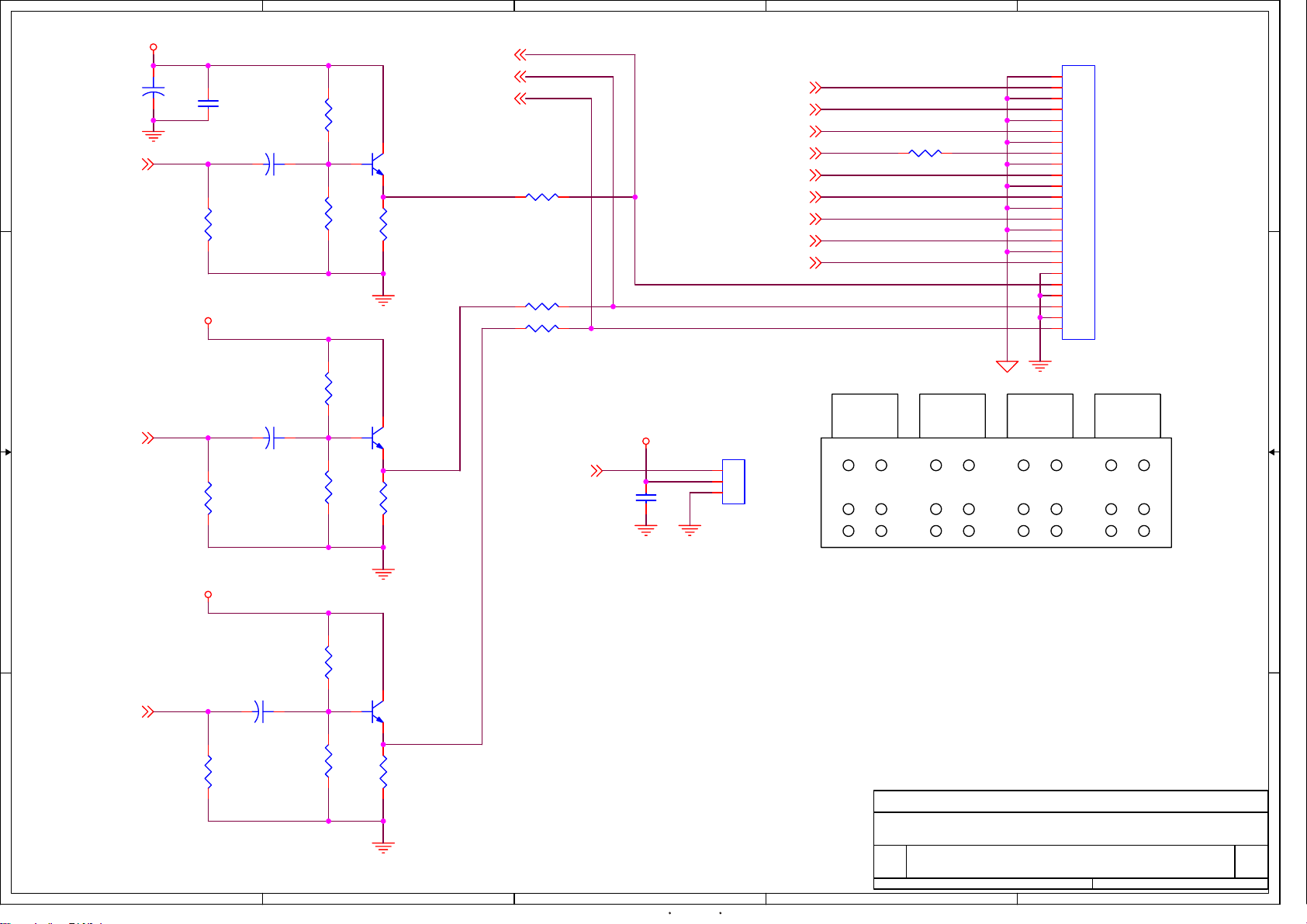
A
B
C
D
E
+5V
R_Cr8
+
C64
10u/16
4 4
R_V_OUT1
C65
104
R98
180
C66
220u/16
+
R94
12K
R97
6.8K
Q14
3904
R99
470
B_Cb8
G_Y8
R96 B221
CENTER_OUT5
REAR_L_OUT4
MIX_L_OUT3,8,9
SPDIF_OUT1
FRONT_L_OUT
R95 B221
MIX_R_OUT3,8,9
MIX_L_OUT3,8,9
SUBWOOFER_OUT5
REAR_R_OUT4
MIX_R_OUT3,8,9
+5V
3 3
R102
12K
C67
220u/16
B_U_OUT1
R104
180
+
R103
6.8K
Q15
3904
R105
470
R100 B221
R101 B221
OPTICAL1
+5V
C68
104
1
2
3
OP1
GP1F32T
FRONT_R_OUT
78
910
11 12
12
34
56
13 14
15 16
17 18
S4
AV12-8.4-2G-2
1
2
3
4
5
6
7
8
9
10
11
12
13
14
15
16
17
18
19
20
21
22
23
24
19 20
21 22
23 24
TOP VIEW
2 2
+5V
R106
12K
C69
220u/16
R108
180
+
R107
6.8K
G_Y_OUT1
1 1
A
Q16
3904
R109
470
B
Title
<Title>
Size Document Number Rev
A4
of
C
D
Date: Sheet
710Friday, January 28, 2005
E
1.0
91
Page 94

A
B
C
D
E
C70 474
SC1_L_IN8
SC1_R_IN8
SC2_L_IN1,8
SC2_R_IN1,8
4 4
BTSC
VCC_AIN
IDC Slave Addr: 0x80/81
C91
152
C80
56PF
C85 10PF
18.432MHz
C89 10PF
TV_MONO
X2
C92
471
BDCOMP
R115
75K
AHVSUP
C79
TV_MONO1,8
TV_IF1
101
R112
1K
3 3
VCC_AIN
+5V
FB1
B601
12
C90
+
10u/16
2 2
FB2
B601
AVSUP
+5V
R214
1 1
A
G+3.3V
*47 1/10W
R216
*150 1/10W
B
C71 474
C83
56PF
CLK_MSP_XIN
CLK_MSP_XOUT
V_G_CON9
Control video
gain of dvd to
vcr.General
this pin is
high,but when
recording dvd
to vcr it is
low.
+5V
IIC_SCL1,2,9
IIC_SDA1,2,9
/RST_BTSC1
C72 474
1
2
3
4
5
6
7
8
9
10
11
DVSUP
+
C93
10u/16
C74 474
+
C76
10u/16
U6
AVSUP
ANA_IN1+
ANA_INTESTEN
XTAL_IN
XTAL_OUT
TP
D_CTR_I/O_1
D_CTR_I/O_0
ADR_SEL
STANDBYQ
C94
103
IIC_SCL
IIC_SDA
C
12
44
AVSS
I2C_SCL
SC1_IN_L
MONO_IN
VREFTOP
SC1_IN_R
I2C_SDA
I2S_CL
I2S_WS
I2S_DA_OUT
39
ASG1
I2S_DA_IN1
SC2_IN_L
SC2_IN_R
TP_CO
DVSUP
37
38
40
41
42
43
1213141516171819202122
G+3.3V
C174
*224
D33
*1N4148
C73 3.3u/50
1 2
+
C75 104
C77
104
R110
*0
12
+
C78
343536
10u/16
AHVSS
AGNDC
CAPL_M
AHVSUP
NC
SC1_OUT_L
SC1_OUT_R
VREF1
NC
DACM_L
DACM_R
VREF2
NC
NC
DVSS
I2S_DA_IN2
RESETQ
MSP34X5G-PMQFP44
G+3.3V
C171
*104
R215 *10K
R123 *220k
R217
220k
33
32
31
30
29
28
27
26
25
24
23
IIC_SCL
IIC_SDA
Q38
*3904
+12V
R111 220
12
C81
104
+
C82
47u/16
D11
8.2V 1/2W
VCR_TV_R 9
VCR_TV_L 9
C87
102
C88
102
R113
12k
R114
12K
R116
10K
C84 474
R117
10K
C86
474
BTSC_AINL 1
BTSC_AINR 1
U13 TQFP-44-GCODE GSV01
NC2
NC3
NC15
NC16
12339456
NC1
/I2C
33
NC0
UART/SIO
IIC Address:30H
44
GND1
43
VDD
42
NC22
41
NC21
40
NC20
NC19
38
NC18
37
VSS1
36
A2
35
A1
34
A0
G+3.3V
G+3.3V
C170
*104
C172 *22PF
12
13
14
15
16
17
18
19
20
21
22
NC8
NC9
NC10
NC11
/SCK
VDD1
SD/TXD
SI/RXD
SCL
SDA
GND2
NC24
NC17
23
NC23
GND
24
VSS
NC7
/RESETX2X1
252627
7891011
NC6
NC4
NC5
VSS0
VDD0
2829303132
Y1
C173
*5MHz
C175
*224
Title
<Title>
Size Document Number Rev
<Doc>
Custom
Date: Sheet
D
*22PF
of
810Friday, January 28, 2005
E
92
Page 95

A
VI_FSS
4 4
R120
SC2_R_OUT
SC2
SCART IN
3 3
SC2_CVBS_OUT
0
R121
SC2_L_OUT
0
1
SC2_R_IN
SC2_L_IN
R134
*B221
SC2_R_IN 1,7
SC2_L_IN 1,7
FB4
B221
FB5 B221
FB6
B221
FB7
B221
D17
MMBD4148SE SOT-23
MIX_L_OUT3,6,9
FB3
B221
SC2_B
AV_CONTROL
SC2_G
SC2_R
VI_FSS
132
SC2_CVBS_IN
5V_STB
MIX_L_OUT
2
3
4
5
6
7
8
9
10
11
12
13
14
15
16
17
18
19
20
21
SC2_L_IN
CVBS2
SC2_CVBS_IN
R138
3.3K
5V_STB
SC2_R_IN
5V_STB
5V_STB
MIX_R_OUT
R137
1K
LOOP_C
Q21
3904
R148
1K
Q23
3904
D19
L
H
MIX_R_OUT3,6,9
D31
1N4148
SC1_CVBS_IN
132
SC1_CVBS_OUT
DECODER
DVD RW
+5V
R141
3.3K
SC1
TO TV
1
2
3
4
5
2 2
6
7
8
9
10
11
12
13
14
15
16
17
18
19
20
21
Fast Blanking Pin16
High(1-3V)
SC1_R_IN 7
SC1_L_IN 7
SC1_R_OUT
SC1_L_OUT
FB10
221
FB11
221
FB12
221
FB9 B221
FB8
B221
RGB
SC1_B
SC1_G
SC1_R
SC1_CVBS_OUT
SC1_CVBS_RGB_SEL
MMBD4148SE SOT-23
CompositeLow(0-0.4V)
E5_GPIOx1_RTC_INT1,2
1 1
Function select(AV CONTROL) Pin8
High(9.5-12V)
Mid(5-8V)
Low(0-2V)
AV mode
Wide-screen
TV mode
E5_GPIO1(for DMN8600) SC2_CVBS_IN
Control by remoter DVDR/TV
A
B
+5V
R221
47K
Q40
R222
3904
1K
132
D13
MMBD4148SE SOT-23
C100
R125
104
4.7K
132
D14
MMBD4148SE SOT-23
R124 22
Q35 3906
5V_STB
R201 100 K
D24 1N4148
D25
+
C164
220u/16
D18
1N4148
1N4148
U10
HC4053
12
13
2
1
5
3
11
10
9
6
7
LOOP_DECODER_C
R140
47K
X0
X1
Y0
Y1
Z0
Z1
A
B
C
EN
VEE
VI_FSS
+5V
D20
1N4148
SCART LOOP AND DECODER Function
STATE
STANDBY/DECODER OFF
POWER ON/DECODER ON
R150
75
D32
1N4148
R151
3.3K
IO
LOOP DECODER OFF_C SC1_AUDIO_OUT
H
L RW_AUDIO_OUT
POWER ON/DECODER OFF
B
R218 1.8K
R219 47K
R202
1K
Q36
3904
168
X
VCCGND
Y
Z
5V_STB
R146
1K
132
E5_GPIOx21
-6.2V
7.5K
14
15
4
R200
4.7K
R182
Q25
3904
Q39
3906
SC2_AUDIO_INE5_GPIOx1
SC2_AUDIO_IN SC1_AUDIO_IN SC2_CVBS_IN RW_RGB_OUTH
R220
3.3K
D15
MMBD4148SE SOT-23
5V_STB
1N4148
R128 4.7K
E5_GPIOx35
5V_STB
C106
C105
104
104
+
C109
10u/16
SC1_CVBS_O
+
C111
10u/16
C119
104
D28
1N4148
Q24
3904
C
CN6
7P1.0
+6.2V
+12V
R129
1K
Q20
3904
1
2
3
4
5
6
7
Q18
3906
R130
4.7K
TV_CVBS_IN1,9
D22
D23
1N4148
SC1_L_OUT
SC1_R_OUT
SC1_L_IN7
D12
1N4148
Q17 3906
R126
1K
Q19
3904
SC2_TO_DVD_B
SC2_TO_DVD_G
SC2_TO_DVD_R
E5_GPIOx35
D16
*1N4148
R127 4.7K
R131
4.7K
TV_MONO1,7
SC1_R_IN7
C120
104
D27
R183
Q22
3904
SC2_AUDIO_OUT
SC1_AUDIO_IN
3.3K
1N4148
Q37
3906
D26
1N4148
SC1_CVBS_OUT
SC2_CVBS_IN
R142
10K
R143
1K
R144
10
L(0--0.4V) H(1--3V)
SC1_RGB
SC2_RGB
SC1_CVBS_RGB_SEL
SC1_AUDIO_IN RW_CVBS_OUT RW_RGB_OUT
C
SC2_G
+6.2V
U11
HC4053
12
X0
13
X1
2
SC1_CVBS_IN
Y0
1
Y1
5
Z0
3
Z1
11
A
10
B
9
C
6
EN
7
VEE
SC1_IN_EN
D29 1N4148
LOOP_DECODER_C
D30 *1N4148
E5_GPIO3(FOR DMN8600)
R145
2.2K
E5_GPIOx4 1
5V_STB
SC1_CVBS_SEL
R180 2.2K
SC2_CVBS_OUT
SC1_CVBS_IN
TUNER_CVBS_IN
SC1_CVBS_IN
VI_FSS
SC2_R
168
VCCGND
R179
7.5K
Q32
3904
R26
R122 0
14
X
15
Y
4
Z
1
2
3
4
5
6
7
8
C167
+
*220u/16
C168
+
VCR_CVBS_OUT9
D
LOOP_C
R_Cr6
SC2_R
SC1_R
G_Y6
SC2_G
SC1_G
5V_STB
SC2_B
C166
*220u/16
C165
104
SC2_TO_DVD_B
+
U8
FSAV330
S
VCC
1B1
OE
4B1
1B2
4B2
1A
4A
2B1
3B1
2B2
3B2
2A
3A
GND
0
SC2_TO_DVD_G
16
15
14
13
12
11
10
9
R25 0
*220u/16
SC2_TO_DVD_R
R132 *0
R_CVBS_IN1
SC2_L_OUT
+
C110
10u/16
SC2_CVBS_O
+
SC2_R_OUT
C114
10u/16
R136
75
SC2_CVBS_IN
R139
75
SC1_CVBS_IN
R135
75
R178
Q33
3904
4.7k
R149
75
REAR/SC2/SC1/VCR_CVBS_SEL HC4052 Pin10,Pin9
Pin10(TVP5146_C7)
Pin9(TVP5146_C8)
L L R_CVBS_IN
LH
L SC1_CVBS_INH
Title
Size Document Number Rev
A3
D
Date: Sheet
E
U7
FSAV330
1
S
2
1B1
3
1B2
4
1A
5
2B1
6
2B2
7
2A
8
GND
VCC
4B1
4B2
3B1
3B2
OE
4A
3A
16
SC1_CVBS_SEL
15
14
13
12
11
10
9
SC2_B
SC1_B
5V_STB
LOOP_C
SC2_CVBS_O
C153
+
*220u/16
C176
*101
5V_STB
SC1_CVBS_O
C154 *220u/16
+
5V_STB
C103
104
C169
101
168
+5V
12
X0
14
X1
15
X2
11
X3
1
Y0
5
Y1
2
Y2
4
Y3
6
INH
10
A
9
B
VDDVSS
13
X
3
Y
U9
74HC4052 SOP
VEE
7
C163
104
SC1_IN_EN
-6.2V
7115/34(5146/C8)
7115/35(5146/C7)
R170
R147
4.7K
4.7K
+5V
Pin13(OUT)
VCR_CVBS_INHH
<Title>
<Doc> <RevCode>
E
5V_STB
C98
104
B_Cb 6
R164
12K
R165
6.8K
R167
12K
C157
104
Q26
3904
SC2_CVBS_OUT
R166
4.7K
C158
104
Q27
3904
SC1_CVBS_OUT
R168
R169
6.8K
4.7K
R_SC2_SC1_CVBS_IN 1,9
TVP5146_C8 1
TVP5146_C7 1
910Friday, January 28, 2005
of
93
Page 96

A
B
C
D
E
+12V
+9V
R152 100 1/4W
C129
C131
223
100u/16
+
R153 100 1/4W
D21
9.1V 1W
4 4
VCR_R_L_IN1
VCR_R_R_IN1
C124 474
C126 474
VCR_TV_R7
VCR_TV_L7
+9V
C123 474
C125 474
MM1313AD
R_SC2_SC1_CVBS_IN1,8
R_Y_IN1
R_C_IN1
F_CVBS_IN1
F_Y_IN1
F_C_IN1
3 3
V_OUT1
V_OUT
C127 104
C130 104
C132 104
C133 104
C135 104
C137 104
R204 2.2K
C138
104
R154 10K
R157
10K
R208 *2.2K
VCR_F_L_IN1
L_OUT3
VCR_F_R_IN1
R_OUT3
C141 474
C144 2.2u/16
+
C146 474
C148 2.2u/16
+
10
11
12
13
14
15
16
17
18
19
20
21
1
2
3
4
5
6
7
8
9
V1-V
V1-L
V1-Y
V1-R
V1-C
S1
V2-V
V2-L
V2-Y
MTV-L
MTV-V
MTV-R
V2-R
V2-C
S2
V3-V
V3-L
NC
STV-V
V3-R
STV-R
NC
STV-L
NC
SCL
SDA
ADR
Cout1
Vcc
Yout1
BIAS
NC
Vout1
Lout1
Rout1
Yin1
GND
Cin1
Mute
Rout2
Vout2
Lout2
42
41
40
39
38
37
C134 2.2u/16
36
35
34
33
32
31
30
29
28
27
26
25
24
23
22
+
U12
C128
104
VCR_L_IN
C136 220u/16
VCR_R_IN
C139 *104
C140 474
C142 474
22u/16
C143
+
R211
*47k
TV_CVBS_IN 1,8
+
R203
*2.2K
VCR_CVBS_OUT
R205
*2.2K
VCR_R_OUT
VCR_L_OUT
R210 1K
+5V
+5V
C155
104
R155
470
R156
1K
Q29
3904
VCR_CVBS_IN
Q34
*3906
R206 *3.9K
R207
*47K
R171
1K
R172
470
V_G_CON 7
MIX_R_OUT 3,6,8
When recording DVD to VCR,put down this pin
to increase the video signal.
Controled by pin 15 of MSP3415.
2 2
IIC_SDA1,2,7
IIC_SCL1,2,7
IIC_SCL
IIC_SDA
VCR_L_IN
VCR_R_IN
R162 100
R163 100
C149 474
C150 474
VCR_CVBS_IN
CN5
10P1.25
1
2
3
+
C145 *220u/16
C147
+
R212 1k
22u/16
R213
*47k
MIX_L_OUT
3,6,8
R161
*6.8K
R173
*6.8K
Q30
*3904
R174
*470
C156
104
MIX_CVBS_OUT 2
R209
0
V_OUT
4
VCR_CVBS_OUT8
VCR_L_OUT1
1 1
VCR_R_OUT1
VCR_CVBS_OUT
VCR_L_OUT
VCR_R_OUT
5
6
7
8
9
10
Title
<Title>
Size Document Number Rev
<Doc> <RevCode>
A
A
B
C
Date: Sheet
D
10 10Friday, January 28, 2005
of
E
94
Page 97

VDD
R11 1K
1
2
CN3
2P2.0
CN4
4P2.0
4
3
2
1
STB_LED
1 1
CN5
K16 SW
4P2.0
4
3
2
1
9DW9919-1
D7
1N4148
VDD
12
+
LD1
STBY
C11
4.7u/16
R16
10K
R9
1K
Q3
9015
K13 SW
K1
K3 S W
K9 SW
R4
10K
VCC
R20
4.7K
VDD
R21
4.7K
321
LD3
VTR
LD2
DVDR
R14
10K
Q1
8050C
Q4
9014
K12
K14 SW
K2
K4 S W
K7 S W
K10 SW
R5
10K
R8 220
R7 220
C15
102
CN1
5P2.0
5
4
3
2
1
R2 1K
R1 2.2 1/4W
C1
VCC
22u/50
K15 SW
K5 SW
K6 SW
K8 SW
K11 SW
R6
10K
U2
HS0038B3V
OUT
VCC
GND
+
F+
F-
-24V
3
2
1
Q2
9015
C2
104
D8
1N4148
D5
1N4148
D1
1N4148
D2
1N4148
D3
1N4148
D4
1N4148
Y1
5MHZ/20pF
C6
30PFC730PF
R15
4.7K
C14
10u/16
C13
103
STB_LED
P_CTL_PSW
C3
103
G7
G8
FIP23
FIP24
P00
P01
P02
P03
P04
P05
P06
P07
IC
X2
X1
VSS0
VDD0
12345678910111213
R12
Y2
100
C10
20PF
5V_STB
D6
C8
103
R13
10
40
41
42
43
44
45
46
47
48
49
50
51
52
VDD
32.768KHZ/20pF
C9
20PF
1N4148
KEYC
KEYB
KEYA
12
+
G6
FIP22
XT1
12
+
FIP21
XT2
G3
G5
G4
FIP18
FIP19
FIP20
U1
UPD16316
RESET
P10
P11
R17
2.7K
VDD
C12
47u/16
G2
A
G1
FIP17
P12
P16
FIP15
FIP16
SCKSOSI
P15
R18
2.7K
G[1:6]
P14
FIP14
FIP13
INTP0
R19
2.7K
27282930313233343536373839
VDD1
VLOAD
INTP1
TI
FIP12
FIP11
FIP10
FIP9
FIP8
FIP7
FIP6
FIP5
FIP4
FIP3
FIP2
FIP1
FIP0
R10
470
P[1:16]
VFD1
20-0607F(1200229)
35
P1
P2
P3
P4
P5
P6
P7
P8
P9
P10
P11
P12
P13
P14
P15
P16
第 1 张
F2
34
F2
32
P16
31
P15
30
P14
29
P13
28
P12
27
P11
26
P10
25
P9
24
P8
23
P7
22
P6
21
P5
20
P4
19
P3
18
P2
17
P1
16
NX
15
NX
14
NX
13
NX
12
NX
11
NX
10
NX
9
1G
8
2G
7
3G
6
4G
5
5G
4
6G
2
F1
1
F1
CN2
10P2.0
1
2
3
4
5
6
7
8
9
10
共 1 张
版次 1.0
F-
-24V
R3
270K
P13
26
P12
25
P11
24
P10
23
P9
22
P8
21
P7
20
P6
19
P5
18
P4
17
P3
16
P2
15
P1
14
VDD
更改
更改单号
设 计
C4
*103
VDD
C5
103
K1 CH+
K2 CH-
K7 VCR
K8 OPEN/CLOSE
K3 EJECT K9 PLAY
K4 DVD
K10 STOP
K5 SOURCE K11 PAUSE
K6 FWD
5V_STB
标准化审 核
日期数量 签名
批 准
K12 REC
D_FM
FP_SCLK
RDY_FM
/FP_RST
D_HOST
ATN_FM
DW9919 panel sch
VFD
4DW9919-2
G1
G2
G3
G4
G5
G6
F+
K13 REV
K14 PREV
K15 NEXT
GND
VFD_DIO
VFD_CLK
VFD_STB
MUTE
5V_STB
/RST_HOST_LED
P_CTL_PSW
D_HOST
ATN_FM
A
95
Page 98

A
6
5
4
3
*221 AC400V
+
IC1
FSDM0565R
Vstr
N.C
Vfb
Vcc
C1
Drain
GND
R5
75 1/4W
1
2
4 4
D10
1N4007
D11
1N4007
D9
1N4007
D12
1N4007
C13
104/~275
RV1
680K/1/2W
BCN1
2P7.92
C14
221 AC400V
1
2
LF1
40mHX2
RT1
10/4A(104MS)
t
D17
22V 1/2W
+
3 3
C3
221 AC400V
2 2
F1
250V/T2AL
CE11
47u/50
CE5
100uF/400V
R1
36K 1/2W
R6
36K 1/2W
C9
473
B
C24
101/500V
L4
FB
D7
HER105
C6
222 AC400V
102/1KV
R2
39K 2W
C4
T1
BCK-28-0605
1
D4
FR207
3
5
6
IC2
PC817
43
12
R15 470
15
14
13
12
11
10
9
8
7
C
HER105
C5
101
D6
D1
HER105
D16
HER105
C19
101/500V
C18 101/500V
C17
101/500V
CE13
47u/50
+
CE12
100u/25
D8
HER105
R14
1.2K
C7
104
IC3
TL431
+
R7
10
D2
HER303
R10
10
D3
SR10100
GZ2200u/10
R13
10
D5
SR10100
+
C10
102
+
L6 30uH
CE18
220U/63V
CE6
C15
104
F-
F+
C12
104
R17
4.7K
R11
8.2K 1%
L1 FB
CE1
100u/25
CE21
10u/50
+
R16
12K 1%
R21
3.3K
Q5
9014
+
+
+
CE2
+
100u/25
2SD669A
D18
27V 1W
L2
10uH
CE3
1000u/25
L3
10uH
CE8
GZ1000u/10
L5
10uH
CE9
GZ2200u/10
B-25V
D13 5.1V 1/2W
R9
47K
*C25
104
+15V
D
Q3
+
+
CE4
470u/25
+
CE10
GZ1000u/10
+
-25V
R8
9.1K 1/6W
CE14
47u/16
C2
104
CE19
100u/50
+
-12V
*150 1/4W
C20
20uH
104
C22
104
Q1
1PP15N03L
R12
Q2
1PP15N03L
R19
10K 1/4W
IC5
TL431
10K 1/4W
Q4
8050
L7
+
+
3
C11
104
CE22
10u/25
GND
CE17
220u/16
+
Vc
+
C23
104
CE20
100u/16
CE23
100u/25
IC4
PQ12RD21
1 2
Vin Vo
+6V
R20
D19
5.6V 1/2W
4
IC6
TL431
R25
1.2K
+26V
GND
+15V
+6V
GND
GND
CE16
100u/25
1.8K 1/4W
+
R22
R24
5.1K 1/4W
5VSTB
C21
104
Q6 9015
321
CN6
6P2.0
1
2
3
4
5
6
R4 1K
+3.3V
D20
for +6V
for +15V
for +26V
C8
104
D14
1N5401
D15
1N5401
CE15
+
220u/16
10K 1/4W
CE7
+
10u/25
-25VB-25V
25V 1/2W
P_CTL
R23
E
+12V
-12V
GND
+12V
GND
+5V
+2.5V/5
+2.5V/G
J9
J13 *7.5MM
R3 10K
5VSTB
+3.3V
+3.3V
+5V
GND
GND
5MM
+12V
+5V
F+
F-
-25V
GND
+5V
CN1
2P2.5
CN2
5P2.5
CN3
10P2.5
1
2
3
4
5
6
7
8
9
10
C16
104
CN4
4P3.96
CN5
5P2.0
1
2
1
2
3
4
5
GND
+12V
1
2
3
4
1
2
3
4
5
TO fan
+5V
1 1
开关电源原理图
数量
审 核
更改单号
标准化
D
签名
批 准
更改
设 计
A
B
C
日期
SWITCH POWER SUPPLY
板号
5DW9919-1
BBK
第 1 张
共 1 张
版次 1.0
广东步步高电子工业有限公司
E
96
Page 99

979899
Page 100

 Loading...