

Page 1

SERVICE MANUAL
DV985S
Page 2

CONTENTS
SAFETY PRECAUTIONS
PREVENTION OF ELECTRO STATIC DISCHARGE(ESD)TO ELECTROSTATICALLY
SENSITIVE(ES)DEVICES
CONTROL BUTTON LOCATIONS AND EXPLANATIONS
PREVERTION OF STATIC ELECTRICITY DISCHARGE
ASSEMBLING AND DISASSEMBLING THE MECHANISM UNIT
OPTICAL PICKUP UNIT EXPLOSED VIEW AND PART LIST
BRACKET EXPLOSED VIEW AND PART LIST
MISCELLANEOUS
ELECTRICAL CONFIRMATION
VI DEO OUTPUT (LUMINANCE SIGNAL) CONFIRMATION
VI DEO OUTPUT(CHROMINANCE SIGNAL) CONFIRMATION
1
1
2
3
4
4
6
7
8
8
9
MPEG BOARD CHECK WAVEFORM
FLI2300 DIGITAL VIDEO CONVERTER DATE SHEET
AM29LV160D
HY57V641620HG
SiI 164 PANELLINK TRANSMITTER
MT1389
SCHEMATIC & PCB WIRING DIAGRAM
SPARE PARTS LIST
10
11
19
24
27
41
44
60
Page 3

1.1 GENERAL GUIDELINES
1. SAFETY PREAUTIONS
2.PREVENTION OF ELECTRO STATIC DISCHARGE(ESD)TO
ELECTROSTATICALLY SENSITIVE(ES)DEVICES
1
1. When servicing, observe the original lead dress. if a short circuit is found, replace all parts which have
been overheated or damaged by the short circuit.
2. After servicing, see to it that all the protective devices such as insulation barrier, insulation papers
shields are properly installed.
3. After servicing, make the following leakage current checks to prevent the customer from being exposed
to shock hazards.
Some semiconductor(solid state)devices can be damaged easily by static electricity. Such components
commonly are called Electrostatically Sensitive(ES)Devices. Examples of typical ES devices are integrated
circuits and some field-effect transistors and semiconductor chip components. The following techniques
should be used to help reduce the incidence of component damage caused by electro static discharge(ESD).
1. Immediately before handling any semiconductor component or semiconductor-equipped assembly, drain
off any ESD on your body by touching a known earth ground. Alternatively, obtain and wear a commercially
availabel discharging ESD wrist strap, which should be removed for potential shock reasons prior to
applying power to the unit under test.
2. After removing an electrical assembly equipped with ES devices,place the assembly on a conductive
surface such as alminum foil, to prevent electrostatic charge buildup or exposure of the assembly.
3. Use only a grounded-tip soldering iron to solder or unsolder ES devices.
4. Use only an anti-static solder removal device. Some solder removal devices not classified as anti-static
(ESD protected)can generate electrical charge sufficient to damage ES devices.
5. Do not use freon-propelled chemicals. These can generate electrical charges sufficient to damage ES
devices.
6. Do not remove a replacement ES device from its protective package until immediately before you are
ready to install it. (Most replacement ES devices are packaged with leads electrically shorted together by
conductive foam, alminum foil or comparable conductive material).
7. Immediately before removing the protective material from the leads of a replacement ES device, touch
the protective material to the chassis or circuit assembly into which the device will be installed.
Caution
Be sure no power is applied to the chassis or circuit, and observe all other safety precautions.
8. Minimize bodily motions when handling unpackaged replacement ES devices. (Otherwise harmless motion
such as the brushing together of your clothes fabric or the lifting of your foot from a carpeted floor can
generate static electricity(ESD).
notice (1885x323x2 tiff)
Page 4
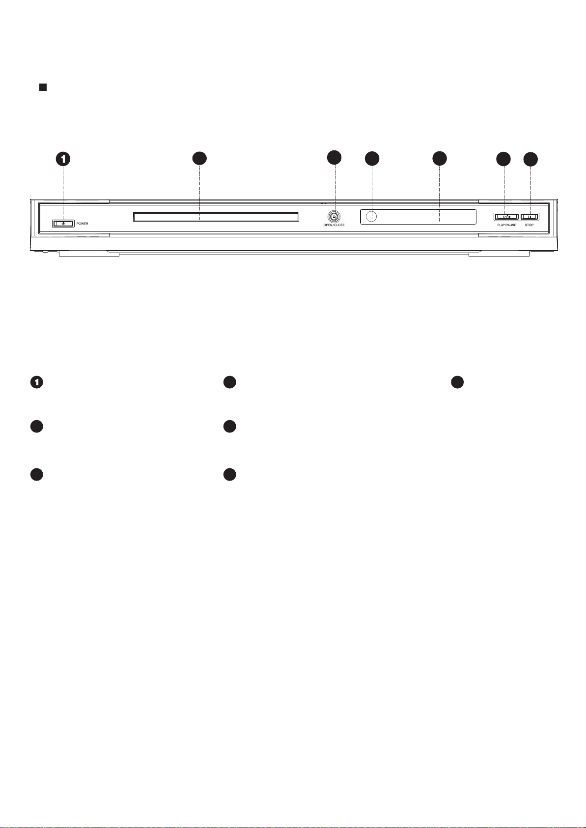
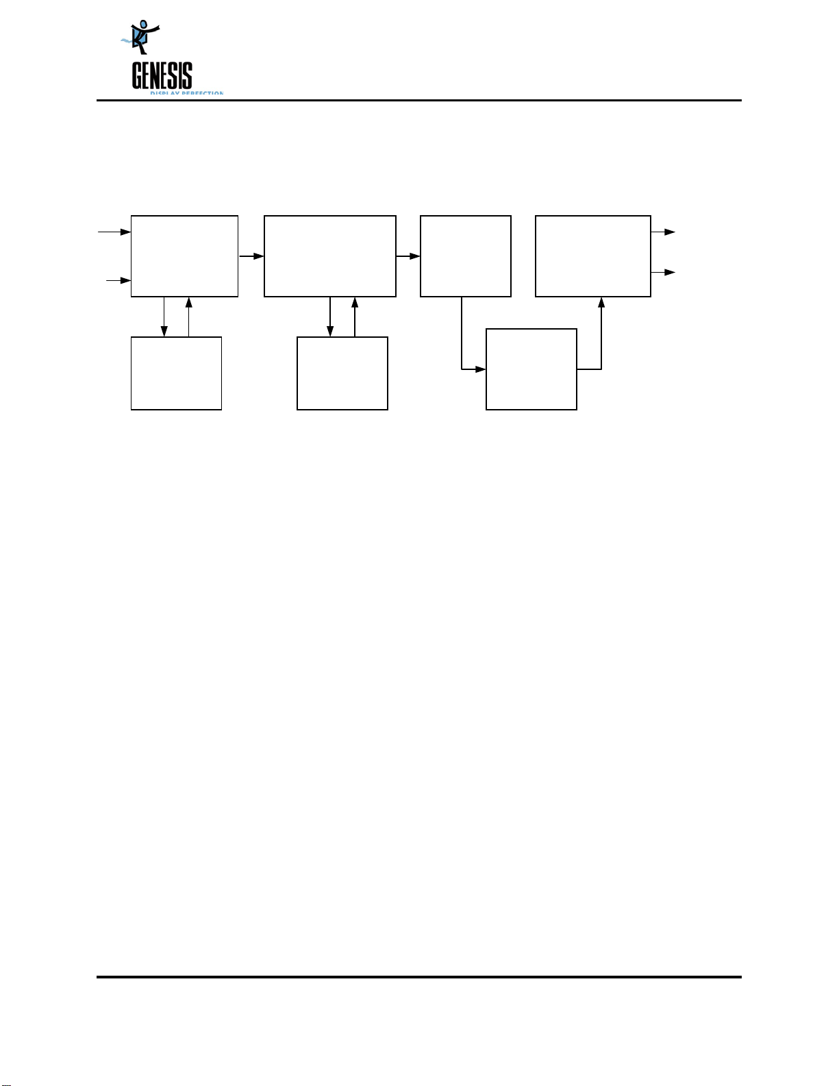
Front Panel Illustration
2
POWER switch
Disc tray
2
2
4
IR SENSOR
5
Display window
3
4
5
7
STOP button
6
7
3
OPEN/CLOSE button
6
PLAY/PAUSE button
Page 5
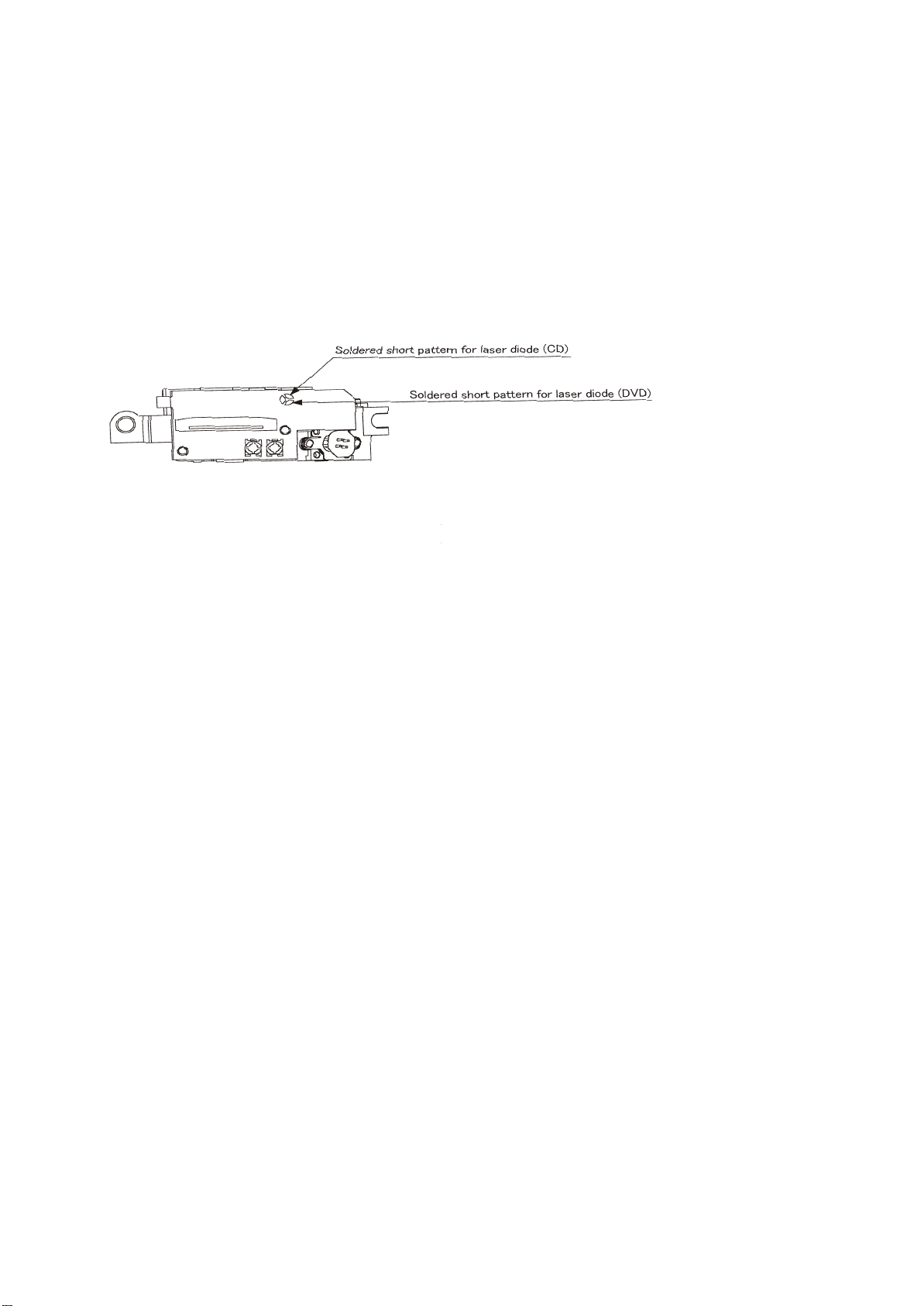
The laser diode in the traverse unit (optical pickup)may brake down due to static electricity of clothes or human
body. Use due caution to electrostatic breakdown when servicing and handling the laser diode.
Some devices such as the DVD player use the optical pickup(laser diode)and the optical pickup will be damaged
by static electricity in the working environment.Proceed servicing works under the working environment where
1. Put a conductive material(sheet)or iron sheet on the area where the optical pickup is placed,and ground the
3. The flexible cable may be cut off if an excessive force is applied to it.Use caution when handling the cable.
3
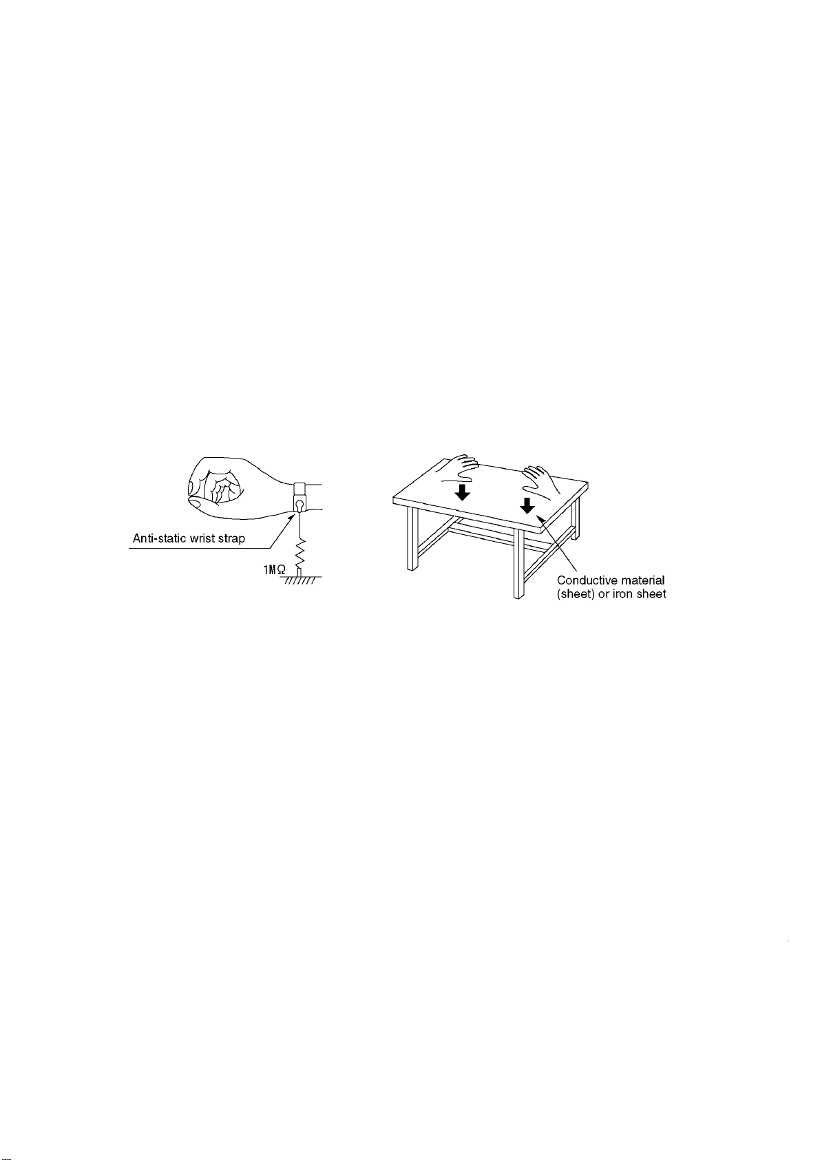
4.PREVENTION OF STATIC ELECTRICITY DISCHARGE
4.1.Grounding for electrostatic breakdown prevention
grounding works is completed.
4.1.1. Worktable grounding
sheet.
4.1.2.Human body grounding
1 Use the anti-static wrist strap to discharge the static electricity from your body.
safety_3 (1577x409x2 tiff)
4.1.3.Handling of optical pickup
1. To keep the good quality of the optical pickup maintenance parts during transportation and before
installation, the both ends of the laser diode are short-circuited.After replacing the parts with new ones,
remove the short circuit according to the correct procedure. (See this Technical Guide).
2. Do not use a tester to check the laser diode for the optical pickup .Failure to do so willdamage the laser
diode due to the power supply in the tester.
4.2. Handling precautions for Traverse Unit (Optical Pickup)
1. Do not give a considerable shock to the traverse unit(optical pickup)as it has an extremely high-precise
structure.
2. When replacing the optical pickup, install the flexible cable and cut is short land with a nipper. See the
optical pickup replacement procedure in this Technical Guide. Before replacing the traverse unit, remove
the short pin for preventingstatic electricity and install a new unit.Connect the connector as short times as
possible.
4. The half-fixed resistor for laser power adjustment cannot be adjusted. Do not turn the resistor.
Page 6
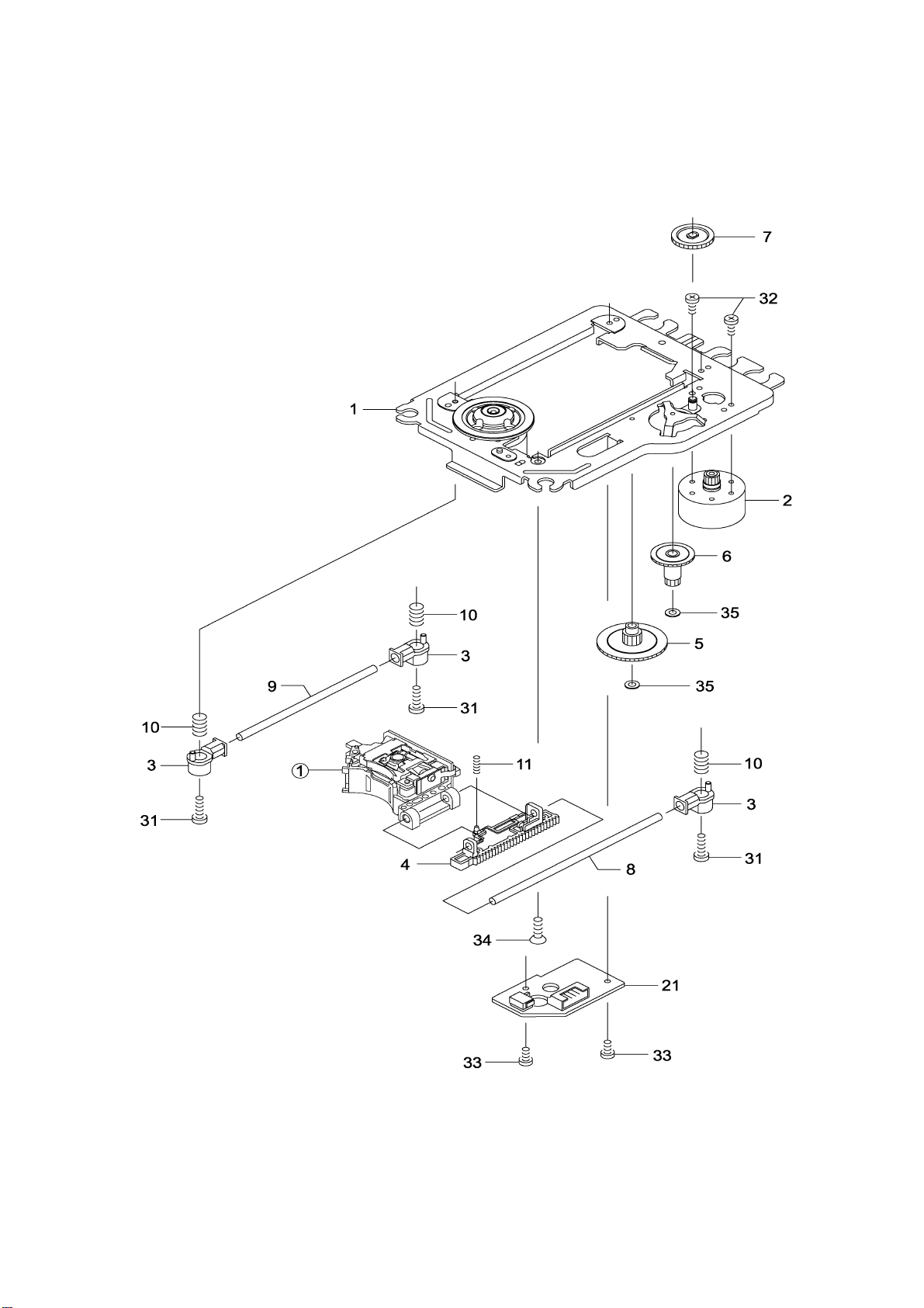
5.1 Optical pickup Unit Explosed View and Part List
5. Assembling and disassembling the mechanism unit
4
Pic (1)
Page 7

Materials to Pic (1)
5
No. PARTS CODE PARTS NAME Q ty
14692200 SF-HD60 1
1
1EA0311A06300 ASSY, CHASSIS, COMPLETE 1
2
Or
3
4
5
6
7
8
9
10
11
21
Or
31
32
1EA0M10A15500 ASSY, MOTOR, SLED 1
1EA0M10A15501 ASSY, MOTOR, SLED 1
1EA2451A24700 HOLDER, SHAFT 3
1EA2511A29100 GEAR, RACK 1
1EA2511A29200 GEAR, DRIVE 1
1EA2511A29300 GEAR, MIDDLE, A 1
1EA2511A29400 GEAR, MIDDLE, B 1
1EA2744A03000 SHAFT, SLIDE 1
1EA2744A03100 SHAFT, SLIDE, SUB 1
1EA2812A15300 SPRING, COMP, TYOUSEI 3
1EA2812A15400 SPRING, COMP, RACK 1
1EA0B10B20100 ASSY, PWB 1
1EA0B10B20200 ASSY, PWB 1
SEXEA25700--- SPECIAL SCREW BIN+-M2X11 3
SEXEA25900--- SPECIAL SCREW M1.7X2.2 2
33
34
35
Note : This parts list is not for service parts supply.
SFBPN204R0SE- SCR S-TPG PAN 2X4 2
SFSFN266R0SE- SCR S-TPG FLT 2.6X6 1
SWXEA15400--- SPECIAL WASHER 1.8X4 X0.25 2
Page 8
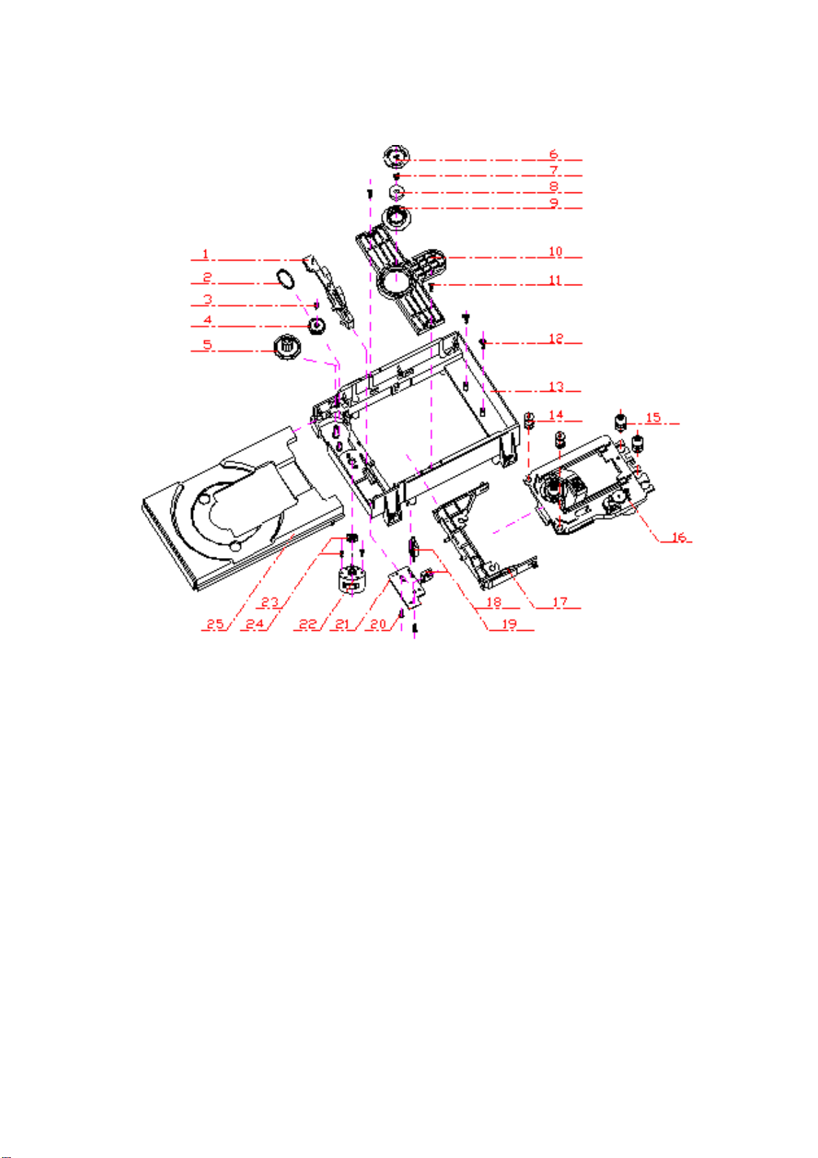
5.2 Bracket Explosed View and Part List
6
Pic (2)
Materials to Pic(2)
1.bracket 14. front silicon rubber
2.belt 15. Back silicon rubber
3.screw 16. Pick-up
4.belt wheel 17. Pick-up
5.gearwheel 18. switch
6.iron chip 19. Five-pin flat plug
7. Immobility mechanism equipment 20. screw
8. Magnet 21. PCB
9. Platen 22. motor
10. Bridge bracket 23. Motor wheel
11. screw 24. screw
12. screw 25.tray
13. Big bracket
Before going process with disassembly and installation, please carefully both
peruse the chart and confirm the materials.
Page 9
5.3 MISCELLANEOUS
7
5.3.1 Protection of the LD(Laser diode)
Short the parts of LD circuit pattern by soldering.
5.3.2 Cautions on assembly and adjustment
Make sure that the workbenches,jigs,tips,tips of soldering irons and measuring instruments are
grounded,and that personnel wear wrist straps for ground.
Open the LD short lands quickly with a soldering iron after a circuit is connected.
Keep the power source of the pick-up protected from internal and external sources of electrical
noise.
Refrain from operation and storage in atmospheres containing corrosive gases (such as H2S,SO2,
NO2 and Cl2)or toxic gases or in locations containing substances(especially from the organic silicon,cyan,
formalin and phenol groups)which emit toxic gases.It is particularly important to ensure that none of the
above substances are present inside the unit.Otherwise,the motor may no longer run.
Page 10
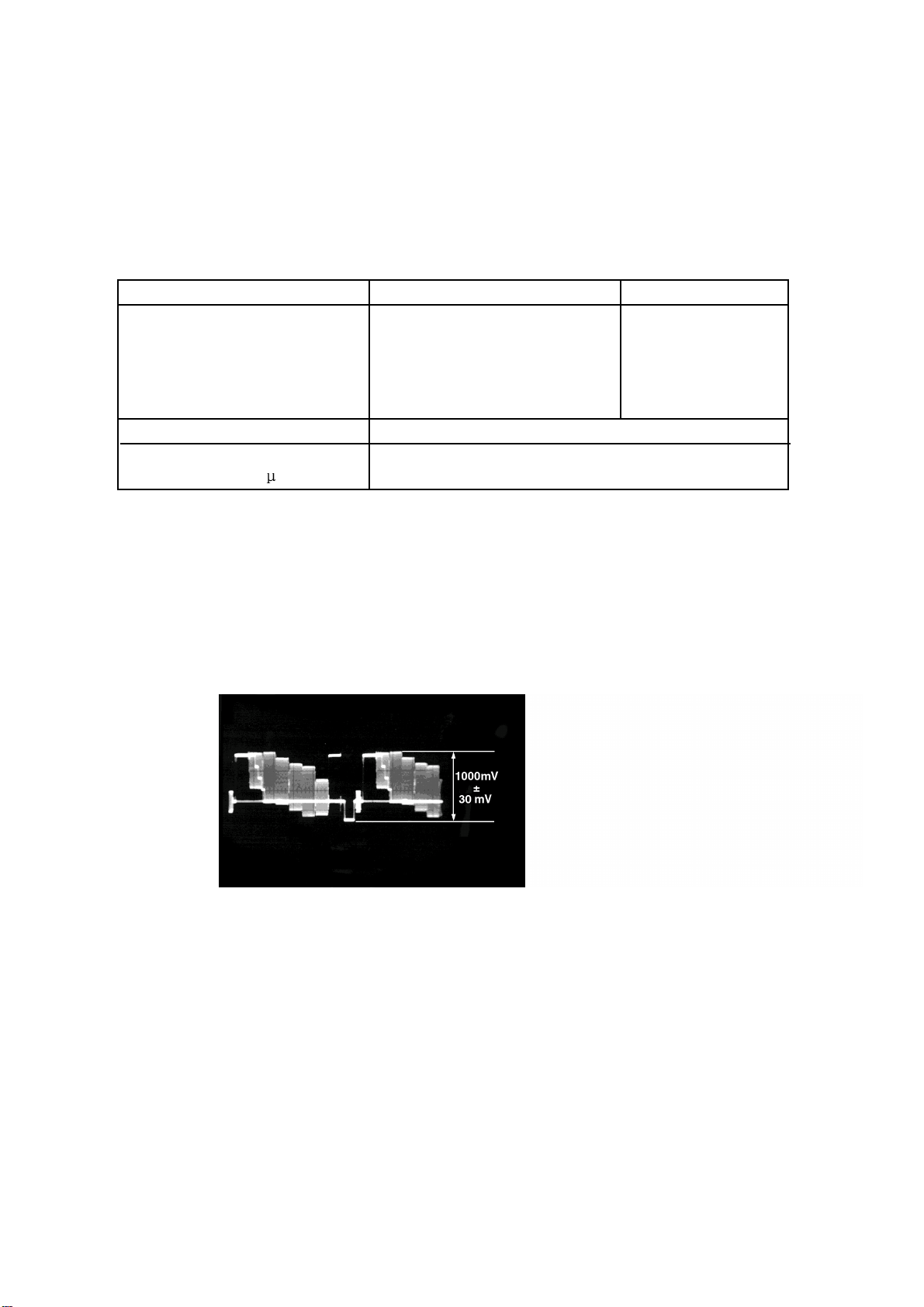
6.1. Video Output (Luminance Signal) Confirmation
6.Electrical Confirmation
8
DO this confirmation after replacing a P.C.B.
Measurement point
Video output terminal
Measuring equipment,tools
200mV/dir,10 sec/dir
Purpose:To maintain video signal output compatibility.
1.Connect the oscilloscope to the video output terminal and terminate at 75 ohms.
2.Confirm that luminance signal(Y+S)level is 1000mVp-p±30mV
PLAY(Title 46):DVDT-S15
PLAY(Title 12):DVDT-S01
Mode Disc
Color bar 75%
Confirmation value
1000mVp-p±30mV
DVDT-S15
or
DVDT-S01
Page 11
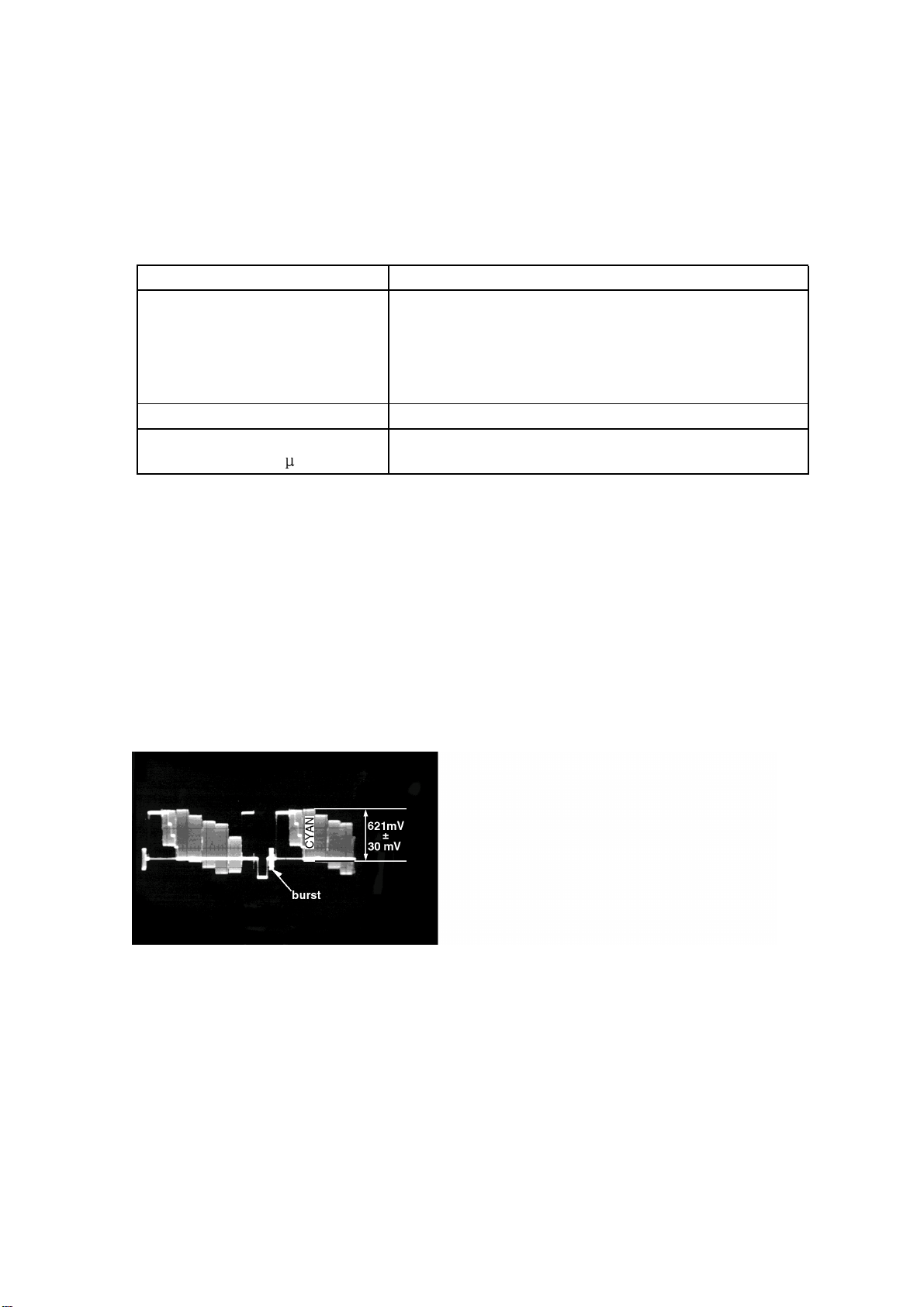
Do the confirmation after replacing P.C.B.
Screwdriver,Oscilloscope
6.2 Video Output(Chrominance Signal) Confirmation
9
Measurement point
Video output terminal
Measuring equipment,tools Confirmation value
200mV/dir,10 sec/dir
Purpose:To maintain video signal output compatibility.
1.Connect the oscilloscope to the video output terminal and terminate at 75 ohme.
2.Confirm that the chrominance signal(C)level is 621 mVp-p±30mV
PLAY(Title 46):DVDT-S15
PLAY(Title 12):DVDT-S01
Mode Disc
Color bar 75%
621mVp-p±30mV
DVDT-S15
or
DVDT-S01
Page 12
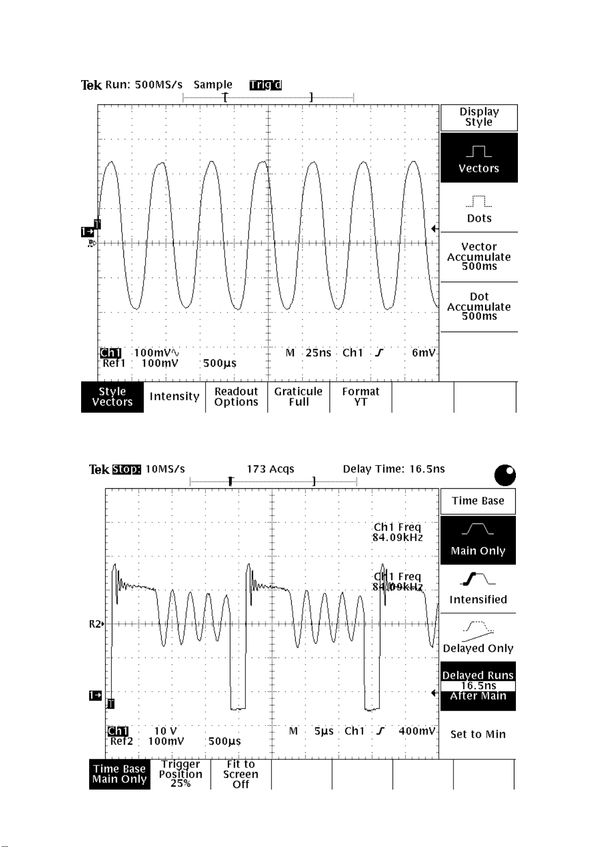
7.MPEG BOARD CHECK WAVEFORM
7.1 27MHz WAVEFORM
7.2 IC5L0380R PIN.2 WAVEFORM DIAGRAM
10
Page 13

FLI2300 Digital Video Converter Data Sheet
11
1 DESCRIPTION
The FLI2300 is a highly integrated digital video
format converter for CRT-TV applications using
patented deinterlacing and post processing algorithms
from Faroudja Laboratories, coupled with highly
flexible scaling, a wide variety of aspect ratio
conversions, and other special video enhancing
features to produce the highest quality image.
1.1 Inputs
• Input all industry standard and non-standard
video resolutions, including 480i (NTSC), 576i
(PAL/SECAM), 480p, 720p, 1080i, and VGA to
XGA
• Digital input, 8-bit Y/Cr/Cb (ITU-R BT656), 8-
bit Y/Pr/Pb, 16-bit Y Cr/Cb (ITU-R BT601), 24bit RGB, YCrCb, YPrPb
• Input pixel rate up to 75MHz maximum
1.2 Outputs
• Output resolutions include 480p, 576p, 720p,
1080i, 1080p, and VGA to SXGA
• Interlaced or Progressive output
• The output can be either analog YUV/RGB
through the integrated 10-bit Digital-To-Analog
Converter (DAC), or digital 24-bit RGB, YCrCb,
YPrPb (4:4:4), or digital 16/20-bit Y Cr/Cb
(4:2:2) Output pixel rate up to 150 MHz
maximum
1.3 Formats
• Input color manipulation matrix supports all
color spaces: RGB, YPrPb, 4:4:4 YCrCb, 4:2:2
YCr/Cb, ITU-R BT656, ITU-R BT601
• Output supports analog RGB, YPrPb, and
YCrCb;
• Output supports digital RGB, YPrPb, 4:4:4
YCrCb and 4:2:2 YCr/Cb
1.4 Frame Rate Conversion
• Tearless Frame Rate Conversion
50/60/72/75/100/120 Hz
1.5 Front End Processing
• Motion Adaptive Noise Reduction - Improves
picture quality for off-air material.
• Cross Color Suppressor (CCS) - Removes cross
color artifacts in composite video signals due to
poor Y/C separation in standard 2-D video
decoders, eliminating the need for expensive 3-D
video decoders.
1.6 Deinterlacing
• Per-pixel Motion Adaptive Deinterlacing
• Patented FilmMode Processing - Used for proper
de-interlacing of 3:2 and 2:2 pulldown material.
• Edit Correction - Film content is continuously
monitored for any break in sequence caused by
“bad edits” and quickly compensates for the
most effective reduction in artifacts.
• DCDi™ by Faroudja - Video is analyzed on a
single pixel granularity to detect presence or
absence of angled lines and edges, which are
then processed to produce a smooth and natural
looking image without visible artifacts or
“jaggies”.
1.7 Scaling
• High Quality Fully Programmable Two
Dimensional Scaler
• Aspect Ratio Conversion for “Anamorphic” or
“Panoramic” (non-linear)
• Display 4:3 images on 16:9 displays and vice
versa, including Letterbox to Fullscreen,
Pillarbox, and Subtitle Display Modes
• Pixel and line dropper to generate PIP windows
1.8 TrueLife™ Enhancer
• Two dimensional, non-linear, luma and chroma
video enhancer brings out details in the picture,
producing a more life-like image.
1.9 Memory
• 32-bit wide SDRAM (i.e. one 2M x 32-bit)
controller, up to 166 MHz operation, for external
SDRAM
*** Genesis Microchip Confidential ***
PRELIMINARY INFORMATION -- SUBJECT TO CHANGE
Page 14
t
12
2 BLOCK DIAGRAMS
Port 2
8-bit
656 Input
Port 1
8/16/24-bit
RGB/YCrCb
Input
Input Processor
with Auto Sync
and auto Adjust
Generation
Clock
PLLs
FLI2300 Digital Video Converter Data Sheet
Figure 2.1: FLI2300– Simplified Internal Block Diagram
Noise Reducer,
Deinterlacer, Frame
Rate Converter and
SDRAM interface
Vertical and
Horizontal
Scalers
2Mx32
SDRAM
(external)
Vertical and
Horizontal
Enhancers
Output
Processor with
Sync Generation
and DACs
16/20/24-bi
RBG/YCrCb
Digital Outputs
RBG/YCrCb
Analog Outputs
*** Genesis Microchip Confidential ***
PRELIMINARY INFORMATION -- SUBJECT TO CHANGE
Page 15
13
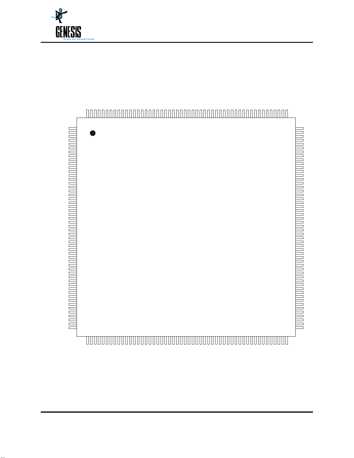
3 PIN INFORMATION
3.1 Pin Diagram
FIELD ID_PORT2
HSYNC_PORT2
VSYNC_PORT2
D1_IN_7
D1_IN_6
D1_IN_5
D1_IN_4
D1_IN_3
D1_IN_2
FLI2300 Digital Video Converter Data Sheet
Figure 3.1: Pinout Information
IN_CLK_PORT2
XTAL IN
XTAL OUT
VDD9
D1_IN_1
VDDcore8
VSScore
TEST2
VSS
D1_IN_0
TEST1
TEST0
DAC_PVDD
DAC_GR_AVDD
DAC_GR_AVSS
DAC_VREFIN
DAC_AVSS
DAC_AVDD
DAC_VREFOUT
DAC_COMP
DAC_RSET
DAC_AVDDR
DAC_AVSSR
DAC_R_OUT
DAC_G_OUT
DAC_AVDDG
DAC_AVSSG
DAC_AVSSB
DAC_B_OUT
DAC_AVDDB
DAC_VSS
DAC_PVSS
DAC_VDD
AVDD_PLL_FE
AVDD_PLL_SDI
AVSS_PLL_FE
AVSS_PLL_SDI
AVSS_PLL_BE2
AVDD_PLL_BE2
AVSS_PLL_BE1
AVDD_PLL_BE1
PLL_PVDD
PLL_PVSS
HSYNC1_PORT1
VSYNC1_PORT1
FIELD ID1_PORT1
IN_CLK1_PORT1
HSYNC2_PORT1
VSYNC2_PORT1
FIELD ID2_PORT1
VDD1
VSS
IN_CLK2_PORT1
B/Cb/D1_0
B/Cb/D1_1
B/Cb/D1_2
B/Cb/D1_3
B/Cb/D1_4
VDDcore1
VSScore
B/Cb/D1_5
B/Cb/D1_6
B/Cb/D1_7
R/Cr/Cb Cr_0
R/Cr/Cb Cr_1
R/Cr/Cb Cr_2
R/Cr/Cb Cr_3
R/Cr/Cb Cr_4
R/Cr/Cb Cr_5
R/Cr/Cb Cr_6
R/Cr/Cb Cr_7
G/Y/Y_0
VDD2
VSS
G/Y/Y_1
G/Y/Y_2
G/Y/Y_3
G/Y/Y_4
VDDcore2
VSScore
G/Y/Y_5
G/Y/Y_6
G/Y/Y_7
IN_SEL
TEST
DEV_ADDR1
DEV_ADDR0
SCLK
SDATA
RESET_N
VDD3
VSS
SDRAM DATA(0)
SDRAM DATA(1)
SDRAM DATA(2)
1 0 0
1 6 0
1 5 5
1 5 0
1 4 5
1 4 0
1 3 5
1 3 0
1 2 5
1 2 0
1 1 5
1 1 0
1 0 5
OE
G/Y/Y_OUT_7
G/Y/Y_OUT_6
G/Y/Y_OUT_5
G/Y/Y_OUT_4
G/Y/Y_OUT_3
G/Y/Y_OUT_2
G/Y/Y_OUT_1
G/Y/Y_OUT_0
VSS
VDD8
R/V/Pr_OUT_7
R/V/Pr_OUT_6
R/V/Pr_OUT_5
R/V/Pr_OUT_4
R/V/Pr_OUT_3
R/V/Pr_OUT_2
VSScore
VDDcore7
R/V/Pr_OUT_1
R/V/Pr_OUT_0
B/U/Pb_OUT_7
B/U/Pb_OUT_6
B/U/Pb_OUT_5
B/U/Pb_OUT_4
B/U/Pb_OUT_3
B/U/Pb_OUT_2
VSS
VDD7
B/U/Pb_OUT_1
B/U/Pb_OUT_0
CLKOUT
VSScore
VDDcore6
CTLOUT4
CTLOUT3
CTLOUT2
CTLOUT1
CTLOUT0
TEST OUT1
TEST OUT0
TEST3
SDRAM CLKIN
VSS
VDD6
SDRAM CLKOUT
SDRAM DQM
SDRAM CSN
SDRAM BA0
SDRAM BA1
SDRAM CASN
SDRAM RASN
1
2 0 5
2 0 0
1 9 5
1 9 0
1 8 5
1 8 0
1 7 5
1 7 0
1 6 5
5
1 0
1 5
2 0
2 5
3 0
3 5
4 0
4 5
5 0
5 5
6 0
6 5
7 0
7 5
8 0
8 5
9 0
9 5
SDRAM DATA(3)
SDRAM DATA(5)
SDRAM DATA(4)
SDRAM DATA(7)
SDRAM DATA(6)
Package: 208-pin PQFP
PRELIMINARY INFORMATION -- SUBJECT TO CHANGE
VSS
VDD4
SDRAM DATA(8)
SDRAM DATA(9)
SDRAM DATA(10)
SDRAM DATA(12)
SDRAM DATA(11)
VSScore
VDDcore3
SDRAM DATA(18)
SDRAM DATA(21)
SDRAM DATA(17)
SDRAM DATA(16)
SDRAM DATA(14)
SDRAM DATA(13)
SDRAM DATA(15)
SDRAM DATA(20)
SDRAM DATA(19)
SDRAM DATA(22)
VSScore
VDDcore4
SDRAM DATA(24)
SDRAM DATA(26)
SDRAM DATA(27)
SDRAM DATA(25)
SDRAM DATA(23)
*** Genesis Microchip Confidential ***
VSS
VDD5
TEST IN
SDRAM DATA(31)
SDRAM DATA(28)
SDRAM DATA(30)
SDRAM DATA(29)
SDRAM ADDR(9)
SDRAM ADDR(10)
VSScore
VDDcore5
SDRAM ADDR(6)
SDRAM ADDR(5)
SDRAM ADDR(7)
SDRAM ADDR(8)
SDRAM ADDR(4)
SDRAM WEN
SDRAM ADDR(3)
SDRAM ADDR(0)
SDRAM ADDR(1)
SDRAM ADDR(2)
Page 16
FLI2300 Digital Video Converter Data Sheet
14
3.2 Pin details
Table 3.1: FLI2300 pin details
Internal
Pull up/
Pulldown
Pin
No
1
HSYNC1_PORT1 Input 5v
2
VSYNC1_PORT1 Input 5v
FIELD ID1_PORT1
3
IN_CLK1_PORT1
4
5
HSYNC2_PORT1 Input 5v
6
VSYNC2_PORT1 Input 5v
FIELD ID2_PORT1
7
VDD1
8
VSS
9
IN_CLK2_PORT1
10
B/Cb/D1_0
11
B/Cb/D1_1
12
B/Cb/D1_2
13
B/Cb/D1_3
14
B/Cb/D1_4
15
VDDcore1
16
VSScore
17
B/Cb/D1_5
18
B/Cb/D1_6
19
B/Cb/D1_7
20
R/Cr/Cb Cr_0
21
R/Cr/Cb Cr_1
22
R/Cr/Cb Cr_2
23
R/Cr/Cb Cr_3
24
R/Cr/Cb Cr_4
25
R/Cr/Cb Cr_5
26
R/Cr/Cb Cr_6
27
R/Cr/Cb Cr_7
28
G/Y/Y_0
29
VDD2
30
VSS
31
G/Y/Y_1
32
G/Y/Y_2
33
G/Y/Y_3
34
G/Y/Y_4
35
VDDcore2
36
VSScore
37
G/Y/Y_5
38
G/Y/Y_6
39
G/Y/Y_7
40
41
IN_SEL Output 5v 8 mA
42 TEST Input 5v
43
DEV_ADDR1 Input 5v
Pin Name I/O Type
Input 5v
Input 5v
Input 5v
Power 3.3 V - Power pin for IO
Ground Ground
Input 5v
Input 5v
Input 5v
Input 5v
Input 5v
Input 5v
Power 1.8 V - Power pin for core
Ground Ground
Input 5v
Input 5v
Input 5v
Input 5v
Input 5v
Input 5v
Input 5v
Input 5v
Input 5v
Input 5v
Input 5v
Input 5v
Power 3.3 V - Power pin for IO
Ground Ground
Input 5v
Input 5v
Input 5v
Input 5v
Power 1.8 V - Power pin for core
Ground Ground
Input 5v
Input 5v
Input 5v
Voltage
Tolerance
Drive
Description
Horizontal sync or reference -CTL1 of Port 1
Vertical sync or reference -CTL1 of Port 1
Odd/Even Field identification -CTL1 of Port 1
Data Clock input -CTL1 of Port 1
Horizontal sync or reference –CTL2 of Port 1
Vertical sync or reference –CTL2 of Port 1
Odd/Even Field identification –CTL2 of Port 1
Data Clock input –CTL2 of Port 1
Port 1 – Digital video input (Blue/Cb/D1)
Port 1 – Digital video input (Blue/Cb/D1)
Port 1 – Digital video input (Blue/Cb/D1)
Port 1 – Digital video input (Blue/Cb/D1)
Port 1 – Digital video input (Blue/Cb/D1)
Port 1 – Digital video input (Blue/Cb/D1)
Port 1 – Digital video input (Blue/Cb/D1)
Port 1 – Digital video input (Blue/Cb/D1)
Port 1 – Digital video input (Red/Cr/CrCb)
Port 1 – Digital video input (Red/Cr/CrCb)
Port 1 – Digital video input (Red/Cr/CrCb)
Port 1 – Digital video input (Red/Cr/CrCb)
Port 1 – Digital video input (Red/Cr/CrCb)
Port 1 – Digital video input (Red/Cr/CrCb)
Port 1 – Digital video input (Red/Cr/CrCb)
Port 1 – Digital video input (Red/Cr/CrCb)
Port 1 – Digital video input (Green/Y)
Port 1 – Digital video input (Green/Y)
Port 1 – Digital video input (Green/Y)
Port 1 – Digital video input (Green/Y)
Port 1 – Digital video input (Green/Y)
Port 1 – Digital video input (Green/Y)
Port 1 – Digital video input (Green/Y)
Port 1 – Digital video input (Green/Y)
Output to select external video mux
Connect to Ground
Device address setting 1
*** Genesis Microchip Confidential ***
PRELIMINARY INFORMATION -- SUBJECT TO CHANGE
Page 17
FLI2300 Digital Video Converter Data Sheet
15
Pin
No
44
DEV_ADDR0 Input 5v
45 SCLK
46 SDATA
47 RESET_N
48 VDD3
49 VSS
50 SDRAM DATA(0)
51 SDRAM DATA(1)
52 SDRAM DATA(2)
53 SDRAM DATA(3)
54 SDRAM DATA(4)
55 SDRAM DATA(5)
56 SDRAM DATA(6)
57 SDRAM DATA(7)
58 SDRAM DATA(8)
59 SDRAM DATA(9)
60 SDRAM DATA(10)
61 SDRAM DATA(11)
62 VDD4
63 VSS
64 SDRAM DATA(12)
65 SDRAM DATA(13)
66 SDRAM DATA(14)
67 SDRAM DATA(15)
68 VDDcore3
69 VSScore
70 SDRAM DATA(16)
71 SDRAM DATA(17)
72 SDRAM DATA(18)
73 SDRAM DATA(19)
74 SDRAM DATA(20)
75 SDRAM DATA(21)
76 SDRAM DATA(22)
77 SDRAM DATA(23)
78 SDRAM DATA(24)
79 SDRAM DATA(25)
80 VDDcore4
81 VSScore
82 SDRAM DATA(26)
83 SDRAM DATA(27)
84 SDRAM DATA(28)
85 SDRAM DATA(29)
86 SDRAM DATA(30)
87 SDRAM DATA(31)
88 VDD5
Pin Name I/O Type
I/O
I/O
Input
Power
Ground
Tristate I/O
Tristate I/O
Tristate I/O
Tristate I/O
Tristate I/O
Tristate I/O
Tristate I/O
Tristate I/O
Tristate I/O
Tristate I/O
Tristate I/O
Tristate I/O
Power
Ground
Tristate I/O
Tristate I/O
Tristate I/O
Tristate I/O
Power
Ground
Tristate I/O
Tristate I/O
Tristate I/O
Tristate I/O
Tristate I/O
Tristate I/O
Tristate I/O
Tristate I/O
Tristate I/O
Tristate I/O
Power
Ground
Tristate I/O
Tristate I/O
Tristate I/O
Tristate I/O
Tristate I/O
Tristate I/O
Power
Voltage
Tolerance
5v 8 mA 2-wire serial control bus clock
5v 8 mA 2-wire serial control bus data
5v PU Reset
3.3 V – Power pin for IO
Ground
5v 4 mA PD
5v 4 mA PD
5v 4 mA PD
5v 4 mA PD
5v 4 mA PD
5v 4 mA PD
5v 4 mA PD
5v 4 mA PD
5v 4 mA PD
5v 4 mA PD
5v 4 mA PD
5v 4 mA PD
3.3 V – Power pin for IO
Ground
5v 4 mA PD
5v 4 mA PD
5v 4 mA PD
5v 4 mA PD
1.8 V - Power pin for core
Ground
5v 4 mA PD
5v 4 mA PD
5v 4 mA PD
5v 4 mA PD
5v 4 mA PD
5v 4 mA PD
5v 4 mA PD
5v 4 mA PD
5v 4 mA PD
5v 4 mA PD
1.8 V – Power pin for core
Ground
5v 4 mA PD SDRAM data bus *
5v 4 mA PD
5v 4 mA PD
5v 4 mA PD
5v 4 mA PD
5v 4 mA PD
3.3 V – Power pin for IO
Drive
Internal
Pull up/
Pulldown
Device address setting 0
SDRAM data bus *
SDRAM data bus *
SDRAM data bus *
SDRAM data bus *
SDRAM data bus *
SDRAM data bus *
SDRAM data bus *
SDRAM data bus *
SDRAM data bus *
SDRAM data bus *
SDRAM data bus *
SDRAM data bus *
SDRAM data bus *
SDRAM data bus *
SDRAM data bus *
SDRAM data bus *
SDRAM data bus *
SDRAM data bus *
SDRAM data bus *
SDRAM data bus *
SDRAM data bus *
SDRAM data bus *
SDRAM data bus *
SDRAM data bus *
SDRAM data bus *
SDRAM data bus *
SDRAM data bus *
SDRAM data bus *
SDRAM data bus *
SDRAM data bus *
SDRAM data bus *
Description
*** Genesis Microchip Confidential ***
PRELIMINARY INFORMATION -- SUBJECT TO CHANGE
Page 18
FLI2300 Digital Video Converter Data Sheet
16
Pin
No
89 VSS
90 TEST IN
91 SDRAM ADDR(10)
92 SDRAM ADDR(9)
93 SDRAM ADDR(8)
94 SDRAM ADDR(7)
95 SDRAM ADDR(6)
96 VDDcore5
97 VSScore
98 SDRAM ADDR(5)
99 SDRAM ADDR(4)
100 SDRAM ADDR(3)
101 SDRAM ADDR(2)
102 SDRAM ADDR(1)
103 SDRAM ADDR(0)
104 SDRAM WEN
105 SDRAM RASN
106 SDRAM CASN
107 SDRAM BA1
108 SDRAM BA0
109 SDRAM CSN
110 SDRAM DQM
111 SDRAM CLKOUT
112 VDD6
113 VSS
114 SDRAM CLKIN
115 TEST3
116 TEST OUT0
117 TEST OUT1
118 CTLOUT0
119 CTLOUT1
120 CTLOUT2
121 CTLOUT3
122 CTLOUT4
123 VDDcore6
124 VSScore
125 CLKOUT
126 B/U/Pb_OUT_0
127 B/U/Pb_OUT_1
128 VDD7
129 VSS
Pin Name I/O Type
Ground
Input
Tristate O/P
Tristate O/P
Tristate O/P
Tristate O/P
Tristate O/P
Power
Ground
Tristate O/P
Tristate O/P
Tristate O/P
Tristate O/P
Tristate O/P
Tristate O/P
Tristate O/P
Tristate O/P
Tristate O/P
Tristate O/P
Tristate O/P
Tristate O/P
Tristate O/P
Output
Power
Ground
Input
Input
Output
Output
Tristate O/P
Tristate O/P
Tristate O/P
Tristate O/P
Tristate O/P
Power
Ground
Tristate O/P
Tristate O/P
Tristate O/P
Power
Ground
Voltage
Tolerance
Ground
5V Test input-Connect to ground
5v 8 mA SDRAM address bus *
5v 8 mA SDRAM address bus *
5v 8 mA SDRAM address bus *
5v 8 mA SDRAM address bus *
5v 8 mA SDRAM address bus *
1.8 V – Power pin for core
Ground
5v 8 mA SDRAM address bus *
5v 8 mA SDRAM address bus *
5v 8 mA SDRAM address bus *
5v 8 mA SDRAM address bus *
5v 8 mA SDRAM address bus *
5v 8 mA SDRAM address bus *
5v 8 mA SDRAM write enable *
5v 8 mA SDRAM row address select *
5v 8 mA SDRAM column address select *
5v 8 mA SDRAM bank select 1*
5v 8 mA SDRAM bank select 0*
5v 4 mA SDRAM CS *
5v 8 mA SDRAM DQM *
5v 12 mA Clock out to SDRAM *
3.3 V - Power pin for IO
Ground
5v Trace delayed SDRAM Clock in
Test input – Connect to ground
12 mA Test output – leave open
8 mA Test output – leave open
5v 8 mA
5v 8 mA
5v 8 mA
5v 8 mA
5v 8 mA
1.8 V - Power pin for core
Ground
5v 12 mA Output data rate clock
5v 8 mA
5v 8 mA
3.3 V – Power pin for IO
Ground
Drive
Internal
Pull up/
Pulldown
Description
Control signal output selectable as HSync1/
CSync/HRef/Monitor coast
Control signal output selectable as
VSync1/CRef/VRef/Film Indicator
Control signal output selectable as Monitor
coast/HRef/VDD_en / HSync2
Control signal output selectable as Film
Indicator/VRef/backlight_en/VSync2
Control signal output selectable as CRef/Field
ID/CSync/Monitor coast
Digital video output – Blue/U/Pb
Digital video output – Blue/U/Pb
*** Genesis Microchip Confidential ***
PRELIMINARY INFORMATION -- SUBJECT TO CHANGE
Page 19
FLI2300 Digital Video Converter Data Sheet
17
Pin
No
130 B/U/Pb_OUT_2
131 B/U/Pb_OUT_3
132 B/U/Pb_OUT_4
133 B/U/Pb_OUT_5
134 B/U/Pb_OUT_6
135 B/U/Pb_OUT_7
136 R/V/Pr_OUT_0
137 R/V/Pr_OUT_1
138 VDDcore7
139 VSScore
140 R/V/Pr_OUT_2
141 R/V/Pr_OUT_3
142 R/V/Pr_OUT_4
143 R/V/Pr_OUT_5
144 R/V/Pr_OUT_6
145 R/V/Pr_OUT_7
146 VDD8
147 VSS
148 G/Y/Y_OUT_0
G/Y/Y_OUT_1
149
G/Y/Y_OUT_2
150
G/Y/Y_OUT_3
151
G/Y/Y_OUT_4
152
G/Y/Y_OUT_5
153
G/Y/Y_OUT_6
154
G/Y/Y_OUT_7
155
156 OE
157 PLL_PVDD
158 PLL_PVSS
159 AVSS_PLL_BE1
160 AVDD_PLL_BE1
161 AVDD_PLL_BE2
162 AVSS_PLL_BE2
163 AVSS_PLL_SDI
164 AVDD_PLL_SDI
165 AVDD_PLL_FE
166 AVSS_PLL_FE
167 DAC_PVSS
168 DAC_VDD
169 DAC_VSS
170 DAC_BOUT
171
DAC_AVDDB
172 DAC_AVSSB
173 DAC_GOUT
174 DAC_AVDDG
Pin Name I/O Type
Tristate O/P
Tristate O/P
Tristate O/P
Tristate O/P
Tristate O/P
Tristate O/P
Tristate O/P
Tristate O/P
Power
Ground
Tristate O/P
Tristate O/P
Tristate O/P
Tristate O/P
Tristate O/P
Tristate O/P
Power
Ground
Tristate O/P
Tristate O/P
Tristate O/P
Tristate O/P
Tristate O/P
Tristate O/P
Tristate O/P
Tristate O/P
Input
Power
Ground
Ground
Power
Power
Ground
Ground
Power
Power
Ground
Ground
Power
Ground
Output
Power
Ground
Output
Power
Voltage
Tolerance
5v 8 mA Digital video output – Blue/U/Pb
5v 8 mA
5v 8 mA
5v 8 mA
5v 8 mA
5v 8 mA
5v 8 mA Digital video output – Red/V/Pr
5v 8 mA Digital video output – Red/V/Pr
1.8 V – Power pin for core
Ground
5v 8 mA
5v 8 mA
5v 8 mA
5v 8 mA
5v 8 mA
5v 8 mA
3.3 V – Power pin for IO
Ground
5v 8 mA Digital video output – Green/Y
5v 8 mA
5v 8 mA
5v 8 mA
5v 8 mA
5v 8 mA
5v 8 mA
5v 8 mA
5v Output data enable for Digital video output
1.8 V – Power pin for PLL pads
Ground for PLL pads
PLL Ground
1.8 V – Power pin for PLL
1.8 V – Power pin for PLL
PLL Ground
PLL Ground
1.8 V – Power pin for PLL
1.8 V – Power pin for PLL
PLL Ground
Ground for DAC pads
1.8 V – Digital power pin for DAC
DAC digital Ground
34 mA Analog B/U output
3.3 V – Analog power pin for B channel
Analog Ground for B channel
34 mA Analog G/Y output
3.3 V – Analog power pin for G channel
Drive
Internal
Pull up/
Pulldown
Description
Digital video output – Blue/U/Pb
Digital video output – Blue/U/Pb
Digital video output – Blue/U/Pb
Digital video output – Blue/U/Pb
Digital video output – Blue/U/Pb
Digital video output – Red/V/Pr
Digital video output – Red/V/Pr
Digital video output – Red/V/Pr
Digital video output – Red/V/Pr
Digital video output – Red/V/Pr
Digital video output – Red/V/Pr
Digital video output – Green/Y
Digital video output – Green/Y
Digital video output – Green/Y
Digital video output – Green/Y
Digital video output – Green/Y
Digital video output – Green/Y
Digital video output – Green/Y
*** Genesis Microchip Confidential ***
PRELIMINARY INFORMATION -- SUBJECT TO CHANGE
Page 20
FLI2300 Digital Video Converter Data Sheet
18
Pin
No
175 DAC_AVSSG
176 DAC_ROUT
177 DAC_AVDDR
178 DAC_AVSSR
179 DAC_COMP
180 DAC_RSET
181 DAC_VREFOUT
182 DAC_VREFIN
183 DAC_AVDD
184 DAC_AVSS
185 DAC_GR_AVSS
186 DAC_GR_AVDD
187 DAC_PVDD
188 TEST0
189 TEST1
190 TEST2
191 XTAL IN
192 XTAL OUT
193 VDD9
194 VSS
195 IN_CLK_PORT 2
196 D1_IN_0
197 VDDcore8
198 VSScore Ground Ground
199 D1_IN_1 Input 5v 4 mA Port 2 - ITU-R BT656 digital data input
200 D1_IN_2 Input 5v 4 mA Port 2 - ITU-R BT656 digital data input
201 D1_IN_3 Input 5v 4 mA Port 2 - ITU-R BT656 digital data input
202 D1_IN_4 Input 5v 4 mA Port 2 - ITU-R BT656 digital data input
203 D1_IN_5 Input 5v 4 mA Port 2 - ITU-R BT656 digital data input
204 D1_IN_6 Input 5v 4 mA Port 2 - ITU-R BT656 digital data input
205 D1_IN_7 Input 5v 4 mA Port 2 - ITU-R BT656 digital data input
206 FIELD ID_PORT 2
207 VSYNC_ PORT 2
208 HSYNC_PORT 2
Note: 1) * - The connection of these pins depends on the type of external SDRAM used. See Appendix 3
Pin Name I/O Type
Ground
Output
Power
Ground
Output
Output
Output
Input
Power
Ground
Ground
Power
Power
Input
Input
Input
Input
Output
Power
Ground
Input
Input
Power
Input
Input
Input
2) For 16/20 bit Y and muxed C output modes see Appendix 2 for pin configuration
Voltage
Tolerance
Analog Ground for G channel
34 mA Analog R/V output
3.3 V – Analog power pin for R channel
Analog Ground for R channel
Compensation for video DACs
Current setting resistor for video DACs
External Voltage reference for video DACs
3.3 V – Analog power pin for DAC
Analog Ground for DAC
Ground for DAC Guard ring
3.3 V – Power pin for DAC Guard ring
3.3 V –Power pin for DAC pads
5v Test pin – connect to ground
5v Test pin – connect to ground
5v Test pin – connect to ground
External parallel crystal oscillator
External parallel crystal oscillator
3.3 V - Power pin for IO
Ground
5v 4 mA Port 2 - Data Clock input
5v 4 mA Port 2 - ITU-R BT656 digital data input
1.8 V – Power pin for core
5v 4 mA Port 2 - Odd/Even Field identification
5v 4 mA Port 2 - Vertical sync or reference
5v 4 mA Port 2 - Horizontal sync or reference
Drive
Internal
Pull up/
Pulldown
Description
1.28 V Internally generated voltage reference for
video DACs
*** Genesis Microchip Confidential ***
PRELIMINARY INFORMATION -- SUBJECT TO CHANGE
Page 21

16 Megabit (2 M x 8-Bit/1 M x 16-Bit)
19
8. Am29LV160D
CMOS 3.0 Volt-only Boot Sector Flash Memory
DISTINCTIVE CHARACTERISTICS
■ Single power supp ly operation
— Full voltage range: 2.7 to 3.6 volt read and write
operations for battery-powered applications
— Regulated voltage range: 3. 0 to 3.6 volt read and
write operations and for compatibility with high
performance 3.3 volt microprocessors
■ Embedded Algorithms
— Embedded Erase algorithm automatically
preprograms and erases the entire chip or any
combination of designated sectors
— Embedded Program algorithm automatically
writes and verifies data at specified addresses
■ Manufactured on 0.23 µm process technology
— Fully compatible with 0.32 µm Am29L V160B de vice
■ High performan c e
— Access times as fast as 70 ns
■ Ultra low power consumption (typical values at
5MHz)
— 200 nA Automatic Sleep mode current
— 200 nA standby mode current
— 9 mA read current
— 20 mA program/erase current
■ Flexible sector architecture
— One 16 Kbyte, two 8 Kbyte, one 32 Kbyte, and
thirty-one 64 Kbyte sectors (byte mode)
— One 8 Kword, two 4 Kword, one 16 Kword, and
thirty-one 32 Kword sectors (word mode)
— Supports full chip erase
— Sector Protection features:
A hardware method of locking a sector to prevent
any program or erase operations within that sector
Sectors can be locked in-system or via
programming equipment
Temporary Sector Unprotect f eature allows code
changes in previously locked sectors
■ Unlock Bypass Program Command
— Reduces overall pr ogramming time when issuing
multiple program command sequences
■ Top or bottom boot block configurations
available
■ Minimum 1,000,000 write cycle guarantee
per sector
■ 20-year data retention at 125°C
— Reliable operation for the life of the system
■ Package option
— 48-ball FBGA
— 48-pin TSOP
— 44-pin SO
■ CFI (Common Flash Interface) compliant
— Provides device-specific information to the
system, allowing host software to easily
reconfigure for different Flash devices
■ Compatibility with JEDEC standards
— Pinout and software compatible with single-
power supply Flash
— Superior inadvertent write protection
■ Data# Polling and toggle bits
— Provides a software method of detec ting program
or erase operation completion
■ Ready/Busy# pin (RY/BY#)
— Provides a hardware method of detecting
program or erase cycle completi on (not av ailable
on 44-pin SO)
■ Erase Suspend/Erase Resume
— Suspends an erase operation t o read data from,
or program data to, a sector that is not being
erased, then resumes the erase operation
■ Hardware reset pin (RESET#)
— Hardware method to reset the devic e to reading
array data
This Data Sheet states AMD’s current technical specifications regarding the Product described herein. This Data
Sheet may be revised by subsequent versions or modificat ions due to changes in technical specif ic ations.
Publication# 22358 Rev: B Amendment/+3
Issue Date: November 10, 2000
Page 22

PRODUCT SELECTOR GUIDE
20
Family Part Number Am29LV160D
Speed Option Voltage Range: V
Max access time, ns (t
Max CE# access time, ns (t
Max OE# access time, ns (t
)7090120
ACC
)7090120
CE
) 303550
OE
= 2.7–3.6 V -70 -90 -120
CC
Note: See “AC Characteristics” for full specifications.
BLOCK DIAGRAM
RY/BY#
V
CC
V
SS
RESET#
WE#
BYTE#
CE#
OE#
State
Control
Command
Register
PGM Voltage
Generator
Sector Switches
Erase Voltage
Generator
Chip Enable
Output Enable
Logic
STB
DQ0
–
DQ15 (A-1)
Input/Output
Buffers
Latch
Data
A0–A19
VCC Detector
Timer
STB
Address Latch
Y-Decoder
X-Decoder
Y-Gating
Cell Matrix
Am29LV160D
Page 23

CONNECTION DIAGRAMS
21
A15
A14
A13
A12
A11
A10
A9
A8
A19
NC
WE#
RESET#
NC
NC
RY/BY#
A18
A17
A7
A6
A5
A4
A3
A2
A1
A16
BYTE#
V
DQ15/A-1
DQ7
DQ14
DQ6
DQ13
DQ5
DQ12
DQ4
V
DQ11
DQ3
DQ10
DQ2
DQ9
DQ1
DQ8
DQ0
OE#
V
CE#
A0
SS
CC
SS
1
2
3
4
5
6
7
8
9
10
11
12
13
14
15
16
17
18
19
20
21
22
23
24
1
2
3
4
5
6
7
8
9
10
11
12
13
14
15
16
17
18
19
20
21
22
23
24
Standard TSOP
Reverse TSOP
48
47
46
45
44
43
42
41
40
39
38
37
36
35
34
33
32
31
30
29
28
27
26
25
48
47
46
45
44
43
42
41
40
39
38
37
36
35
34
33
32
31
30
29
28
27
26
25
A16
BYTE#
V
SS
DQ15/A-1
DQ7
DQ14
DQ6
DQ13
DQ5
DQ12
DQ4
V
CC
DQ11
DQ3
DQ10
DQ2
DQ9
DQ1
DQ8
DQ0
OE#
V
SS
CE#
A0
A15
A14
A13
A12
A11
A10
A9
A8
A19
NC
WE#
RESET#
NC
NC
RY/BY#
A18
A17
A7
A6
A5
A4
A3
A2
A1
Page 24

CONNECTION DIAGRAMS
22
RESET#
A18
A17
A7
A6
A5
A4
A3
A2
A1
A0
CE#
V
OE#
DQ0
DQ8
DQ1
DQ9
DQ2
DQ10
DQ3
DQ11
SS
10
11
12
13
14
15
16
17
18
19
20
21
22
1
2
3
4
5
6
7
8
9
SO
44
43
42
41
40
39
38
37
36
35
34
33
32
31
30
29
28
27
26
25
24
23
WE#
A19
A8
A9
A10
A11
A12
A13
A14
A15
A16
BYTE#
V
SS
DQ15/A-1
DQ7
DQ14
DQ6
DQ13
DQ5
DQ12
DQ4
V
CC
FBGA
Top View, Balls Facing Down
A6 B6 C6 D6 E6 F6 G6 H6
A5 B5 C5 D5 E5 F5 G5 H5
A4 B4 C4 D4 E4 F4 G4 H4
A3 B3 C3 D3 E3 F3 G3 H3
A2 B2 C2 D2 E2 F2 G2 H2
A1 B1 C1 D1 E1 F1 G1 H1
Special Handling Instructions
Special handling is required for Flash Memory products
in FBGA packages.
BYTE#A16A15A14A12A13
DQ15/A-1 V
SS
DQ13 DQ6DQ14DQ7A11A10A8A9
V
CC
DQ4DQ12DQ5A19NCRESET#WE#
DQ11 DQ3DQ10DQ2NCA18NCRY/BY#
DQ9 DQ1DQ8DQ0A5A6A17A7
CE#A0A1A2A4A3
OE# V
SS
Flash memory devices in FBGA packages may be
damaged if exposed to ultrasonic cleaning methods.
The package and/or data integrity may be compromised
if the package body is exposed to temperatures above
150°C for prolonged periods of time.
A
Page 25

PIN CONFIGURATION
23
A0–A19 = 20 addresses
DQ0–DQ14 = 15 data inputs/outputs
DQ15/A-1 = DQ15 (data input/output, word mode),
A-1 (LSB address input, byte mode)
BYTE# = Selects 8-bit or 16-bit mode
CE# = Chip enable
OE# = Output enable
WE# = Write enable
RESET# = Hardware reset pin
RY/BY# = Ready/Busy output
(N/A SO 044)
= 3.0 volt-only single power supply
V
CC
(see Product Selector Guide for speed
options and voltage supply toleranc es)
LOGIC SYMBOL
20
A0–A19
CE#
OE#
WE#
RESET#
BYTE# RY/BY#
16 or 8
DQ0–DQ15
(A-1)
(N/A SO 044)
V
SS
= Device ground
NC = Pin not connected internally
Page 26

HY57V641620HG
8.1 HY57V641620HG
24
4 Banks x 1M x 16Bit Synchronous DRAM
DESCRIPTION
The Hyundai HY57V641620HG is a 67,108,864-bit CMOS Synchronous DRAM, ideally suited for the main memory applications which
require large memory density and high bandwidth. HY57V641620HG is organized as 4banks of 1,048,576x16.
HY57V641620HG is offering fully synchronous operation referenced to a positive edge of the clock. All inputs and outputs are synchronized with the rising edge of the clock input. The data paths are internally pipelined to achieve very high bandwidth. All input and output
voltage levels are compatible with LVTTL.
Programmable options include the length of pipeline (Read latency of 2 or 3), the number of consecutive read or write cycles initiated
by a single control command (Burst length of 1,2,4,8 or Full page), and the burst count sequence(sequential or interleave). A burst of
read or write cycles in progress can be terminated by a burst terminate command or can be interrupted and replaced by a new burst
read or write command on any cycle. (This pipelined design is not restricted by a `2N` rule.)
FEATURES
• Single 3.3±0.3V power supply
• All device pins are compatible with LVTTL interface
• JEDEC standard 400mil 54pin TSOP-II with 0.8mm
of pin pitch
• All inputs and outputs referenced to positive edge of
system clock
• Data mask function by UDQM or LDQM
• Internal four banks operation
Note)
• Auto refresh and self refresh
• 4096 refresh cycles / 64ms
• Programmable Burst Length and Burst Type
- 1, 2, 4, 8 or Full page for Sequential Burst
- 1, 2, 4 or 8 for Interleave Burst
• Programmable CAS Latency ; 2, 3 Clocks
.
Page 27

PIN CONFIGURATION
25
HY57V641620HG
VDD
DQ0
VDDQ
DQ1
DQ2
VSSQ
DQ3
DQ4
VDDQ
DQ5
DQ6
VSSQ
DQ7
DD
V
LDQM
/WE
/CAS
/RAS
/CS
BA0
BA1
A10/AP
A0
A1
A2
A3
DD
V
1
2
3
4
5
6
7
8
9
10
11
12
13
14
15
16
17
18
19
20
21
22
23
24
25
26
27
54pin TSOP II
400mil x 875mil
0.8mm pin pitch
VSS
54
DQ15
53
VSSQ
52
DQ14
51
DQ13
50
VDDQ
49
DQ12
48
DQ11
47
VSSQ
46
DQ10
45
DQ9
44
VDDQ
43
DQ8
42
SS
V
41
NC
40
UDQM
39
CLK
38
CKE
37
NC
36
A11
35
A9
34
A8
33
A7
32
A6
31
A5
30
A4
29
SS
V
28
PIN DESCRIPTION
PIN PIN NAME DESCRIPTION
CLK Clock
CKE Clock Enable
CS Chip Select Enables or disables all inputs except CLK, CKE and DQM
BA0,BA1 Bank Address
A0 ~ A11 Address
Row Address Strobe,
RAS, CAS, WE
LDQM, UDQM Data Input/Output Mask Controls output buffers in read mode and masks input data in write mode
DQ0 ~ DQ15 Data Input/Output Multiplexed data input / output pin
VDD/VSS Power Supply/Ground Power supply for internal circuits and input buffers
VDDQ/VSSQ Data Output Power/Ground Power supply for output buffers
NC No Connection No connection
Column Address Strobe,
Write Enable
The system clock input. All other inputs are registered to the SDRAM on the
rising edge of CLK
Controls internal clock signal and when deactivated, the SDRAM will be one
of the states among power down, suspend or self refresh
Selects bank to be activated during RAS activity
Selects bank to be read/written during CAS activity
Row Address : RA0 ~ RA11, Column Address : CA0 ~ CA7
Auto-precharge flag : A10
RAS, CAS and WE define the operation
Refer function truth table for details
Page 28

FUNCTIONAL BLOCK DIAGRAM
I/O Buffer & Logic
26
1Mbit x 4banks x 16 I/O Synchronous DRAM
HY57V641620HG
Self refresh logic
CLK
CKE
CS
RAS
CAS
WE
UDQM
LDQM
& timer
Row active
State Machine
refresh
Column
Active
Internal Row
counter
Row
Pre
Decoders
Column
Pre
Decoders
1Mx16 Bank 3
X decoders
1Mx16 Bank 2
X decoders
X decoders
1Mx16 Bank 1
1Mx16 Bank 0
X decoders
Memory
Y decoders
Cell
Array
Sense AMP & I/O Gate
DQ0
DQ1
DQ14
DQ15
Bank Select
A0
A1
A11
BA0
BA1
Address buffers
Address
Registers
Mode Registers
Column Add
Counter
Burst
Counter
CAS Latency
Data Out Control
Pipe Line Control
Page 29

SiI 164 PanelLink
27
PanelLink Transmitter September 2002
PanelLinkPanelLink
Data Sheet
General Description
The SiI 164 transmitter uses PanelLink
technology to support displays ranging from VGA to
UXGA resolutions (25 - 165Mpps) in a single link
interface.
®
Digital
Features
• Scaleable Bandwidth: 25 - 165MHz Flexible
• Graphics Controller Interface: 12-bit or 24-bit
• Flexible Input Clocking: Single clock single
The SiI 164 transmitter has a highly flexible interface
with either a 12-bit mode (½ pixel per clock edge) or
24-bit mode 1 pixel per clock edge input for true color
• I
• Low Voltage Interface: 3.3V with option for 1.0
(16.7 million) support. In 24-bit mode, the SiI 164
supports single or dual edge clocking. In 12-bit mode,
• Monitor Detection supported through hot plug
the SiI164 supports dual edge single clocking or
single edge dual clocking. The SiI 164 can be
programmed though an I
2
C interface. In addition the
SiI 164 also supports Receiver and Hot Plug
• De-skewing Option varies input clock to input
• Low Power: 3.3V operation (120mA max.) and
Detection.
PanelLink Digital technology simplifies PC design by
• Cable Distance Support: over 5m with twisted
resolving many of the system level issues associated
with high-speed mixed signal design, providing the
• Compliant with DVI 1.0 (DVI is backwards
system designer with a digital interface solution that is
quicker to market and lower in cost.
• Standard and Pb-free packages (see pg 29)
mode 1 pixel/clock inputs
edge (24-bit), Single clock dual edge (12-/24bit), Dual clock single edge (12-bit)
2
C Slave Programming Interface up to 100kHz
to 3.0V Low Voltage Signal Mode
and receiver detection
data timing
Power Down mode (1mA max.)
pair and fiber-optics ready
compliant with VESA
®
P&DTM and DFP)
SiI 164 Pin Diagram
AGND
VCC
RESERVED
DKEN
D23
D22
D21
D20
D19
D18
D17
D16
D15
D14
D13
D12
GND
32
33
34
35
36
37
38
39
40
41
42
43
44
45
46
47
48
49
TX2+
31
50
TX2-
30
51
AVCC
29
52
TX1-
TX1+
27
28
64-Pin TQFP
54
53
TX0-
TX0+
AGND
24
25
26
SiI
164
(Top View)
55
56
57
AVCC
23
58
TXC+
22
59
TXC-
21
60
AGND
20
61
PVCC1
EXT_SWING
18
19
62
63
PGND
17
16
15
14
13
12
11
10
9
8
7
6
5
4
3
2
1
64
GND
BSEL/SCL
DSEL/SDA
ISEL/RST#
VCC
MSEN
PD#
EDGE/HTPLG
CTL1/A1/DK1
CTL2/A2/DK2
CTL3/A3/DK3
VSYNC
HSYNC
VREF
DE
VCC
D9
D8
D7
PVCC2
D11
D10
D6
IDCK-
IDCK+
D5
D4
D3
D2
D1
D0
GND
Figure 1. Pin Diagram for SiI 164
Page 30

SiI 164 PanelLink Transmitter
G
28
Data Sheet
Functional Description
The SiI 164 is a DVI 1.0 compliant PanelLink transmitter in a compact package. It provides 24 bits for data Input to
allow for panel support up to UXGA resolution. Figure 2 shows the functional blocks of the chip.
TX0+
TX1+
TX2+
EXT_SWIN
I2C
Slave
Machine
MSEN
Registers
&
Configuration
Logic Block
TXC+
PanelLink
PanelLink
PanelLinkPanelLink
Digital
core
SDA
SCL
A[3:1]
ISEL/RST
PD
DSEL/SDA
EDGE/HTPLG
DKEN
BSEL/SCL
CTL/A/DK[3:1]
Data Capture
Logic Block
DE
D[23:0]
VSYNC
HSYNC
IDCK+
VREF
IDCK-
Figure 2. Functional Block Diagram
PanelLink TMDS Digital Core
The PanelLink TMDS core encodes video information onto three TMDS differential data lines and the differential
clock. The video data is input by the Data Capture Logic Block, as a 12- or 24-bit bus, using one or two clocks with
one or two edges per clock. An attached monitor may be sensed using the HTPLG pin or internally with Receiver
Sense. This detected state may be output onto the MSEN pin. The device may be powered down using the PD#
pin or with an internal register. The SiI 164 is reset using the ISEL/RST# pin. A resistor tied to the EXT_SWING
pin is used to control the TMDS swing amplitude.
I2C Interface and Registers
The SiI 164 uses a slave I
the switching levels from the host are not 3.3V, then a voltage level shifter must be used. See Figure 16 and
Figure 17 on page 24 for a system diagram.
2
C interface, capable of running at 100kHz. The slave I2C interface is not 5V tolerant. If
A connected display may be detected using the DVI Hot Plug signal, attached to the HTPLG pin; or with the
Receiver Sense logic internal to the SiI 164. The state of the detection, or an interrupt signal indicating a change of
state, may be sent to the MSEN pin. This is useful to the host controller monitoring the SiI 164.
Page 31

SiI 164 PanelLink Transmitter
29
Data Sheet
Data Capture Logic
Video data is input to the SiI 164 by way of a 12-bit or 24-bit interface. The functionality of this interface is affected
by several of the configuration register settings, as follows.
• BSEL selects between 12-bit and 24-bit input bus widths.
• DSEL selects between single-edge and dual-edge modes for the input clocks.
• EDGE selects between rising and falling edge on the input clocks.
• CLK+ and CLK- provide the one or two clocks required for latching the input data bus.
• The PD# input selects the chip power down mode and allows for disabling of the TMDS outputs.
The ISEL/RST# input resets the HDCP engine and internal registers and is asserted after power up and receipt of
a stable input pixel clock.
Page 32

SiI 164 PanelLink Transmitter
30
Data Sheet
Electrical Specifications
Absolute Maximum Conditions
Absolute Maximum Conditions are defined as the worst case conditions the part will tolerate without sustaining
damage. Permanent device damage may occur if absolute maximum conditions are exceeded. Proper operation
under these conditions is not guaranteed. Functional operation should be restricted to the conditions described
under Normal Operating Conditions.
Symbol Parameter Min Typ Max Units
VCC Supply Voltage 3.3V -0.3 4.0 V
VI Input Voltage -0.3 VCC+ 0.3 V
VO Output Voltage -0.3 VCC+ 0.3 V
TJ Junction Temperature (with power applied) 125
T
Storage Temperature -65 150
STG
Normal Operating Conditions
Symbol Parameter Min Typ Max Units
VCC Supply Voltage 3.0 3.3 3.6 V
V
Supply Voltage Noise 100 mV
CCN
TA Ambient Temperature (with power applied) 0 25 70
θ
Note
1. Airflow at 0m/s.
JA
Thermal Resistance (Junction to Ambient)1 64
P-P
°C
°C/W
°C
°C
Digital I/O Specifications
Under normal operating conditions unless otherwise specified.
Symbol Parameter Conditions Min Typ Max Units
VIH High Swing High-level Input
V
REF = VCC
Voltage
VIL High Swing Low-level Input
V
REF = VCC
Voltage
2
V
Low Swing Voltage 1 3.0 V
DDQ
VSH Low Swing High-level Input
V
REF = VDDQ
Voltage
VSL Low Swing Low-level Input
V
REF = VDDQ
Voltage
V
Input Clamp Voltage1 I
CINL
V
Input Clamp Voltage1 I
CIPL
= -18mA GND -0.8 V
CL
= 18mA VCC + 0.8 V
CL
IIL Input Leakage Current -10 10
VIH High Swing High-level Input
V
REF = VCC
Voltage
Notes
1. Guaranteed by design. Voltage undershoot or overshoot cannot exceed absolute maximum conditions
2. VDDQ defines the maximum voltage level of Low Swing input. It is not an actual input voltage. Chip characterization for
Low Swing operation is performed at 1.5V only. Voltage level of Low Swing input should never exceed absolute
maximum rating.
2.0 V
0.8 V
/2 V
/2 V
2.0 V
/2 +
DDQ
300mV
V
DDQ
/2 –
V
100mV
µA
Page 33

SiI 164 PanelLink Transmitter
31
Data Sheet
DC Specifications
Under normal operating conditions unless otherwise specified.
Symbol Parameter Conditions Min Typ Max Units
VOD Differential Voltage Single ended
R
LOAD
= 50Ω, R
EXT_SWING
peak to peak amplitude
V
Differential High-level Output AVCC V
DOH
Voltage1
I
Differential Output Short Circuit
DOS
I
Power-down Current2 0.2 1.0 mA
PD#
I
Transmitter Supply Current IDCK= 165 MHz, 1-pixel/clock
CCT
Current
1
= 0 V 5
V
OUT
mode, R
EXT_SWING
= 510Ω,
IVCC = VCC,
Worst Case Pattern
Notes
1. Guaranteed by design.
2. Assumes all inputs to the transmitter are not toggling.
3. Black and white checkerboard pattern, each checker is one pixel wide.
3
= 510Ω
510 550 590 mV
µA
85
120
mA
Page 34

SiI 164 PanelLink Transmitter
32
Data Sheet
AC Specifications
Under normal operating conditions unless otherwise specified.
Symbol Parameter Conditions Min Typ Max Units Figure
T
IDCK Period, 1-pixel/clock 6 40 ns
CIP
F
IDCK Frequency, 1-pixel/clock 25 165 MHz
CIP
T
IDCK High Time at 165MHz 2.0 ns
CIH
T
IDCK Low Time at 165MHz 2.0 ns
CIL
T
Worst Case IDCK Clock Jitter
IJIT
T
Data, DE, VSYNC, HSYNC
SIDF
Setup Time to IDCK falling edge
(Default De-skew Setting)
T
Data, DE, VSYNC, HSYNC
HIDF
Hold Time from IDCK falling edge
(Default De-skew Setting)
T
Data, DE, VSYNC, HSYNC
SIDR
Setup Time to IDCK rising edge
(Default De-skew Setting)
T
Data, DE, VSYNC, HSYNC
HIDR
Hold Time from IDCK rising edge
(Default De-skew Setting)
T
Data, DE, VSYNC, HSYNC
SID
Setup Time to IDCK falling/rising edge
(Default De-skew Setting)
T
Data, DE, VSYNC, HSYNC
HID
Hold Time from IDCK falling/rising edge
(Default De-skew Setting)
T
VSYNC, HSYNC Delay from DE falling
DDF
T
VSYNC, HSYNC Delay to DE rising edge1 1T
DDR
T
DE high time1 8191T
HDE
T
DE low time1 128T
LDE
T
De-skew step size increment DKEN = 1 260 ps
STEP
T
Duration of RESET signal Low required for
RESET
edge
1
2,3
2 ns
Single Edge
1.0 ns
(DSEL = 0,
EDGE = 0)
Single Edge
0.9 ns
(DSEL = 0,
EDGE = 0)
1
Single Edge
(DSEL = 0,
1.0 ns
EDGE = 1)
1
Single Edge
(DSEL = 0,
0.9 ns
EDGE = 1)
1
Dual Edge
(DSEL = 1,
0.6 ns
BSEL = 0)
1
Dual Edge
(DSEL = 1,
1.3 ns
BSEL = 0)
1T
ns
CIP
ns
CIP
ns
CIP
ns
CIP
10 µs
valid Reset
I2CDVD
S
HLT
SDA Data Valid Delay from SCL high
to low transition
3
Differential Swing High-to-Low Transition
Time
CL = 10pf 700 ns T
C
= 400pf 2000 ns
L
R
LOAD
R
EXT_SWING
= 50Ω,
=
170 200 230 ps
510Ω
S
Differential Swing Low-to-High Transition
LHT
Time
R
LOAD
R
EXT_SWING
= 50Ω,
=
170 200 230 ps
510Ω
Notes
1. Guaranteed by design.
2. Actual jitter tolerance may be higher depending on the frequency of the jitter.
3. All Standard mode I2C (100kHz) timing requirements are guaranteed by design. Fast mode I2C (400kHz) timing
requirements are guaranteed at 10pf loading.
Figure 3
Figure 3
Figure 3
Figure 6
Figure 6
Figure 6
Figure 6
Figure 7
Figure 7
Figure 8
Figure 8
Figure 5
Figure 9
Figure 4
Figure 4
Page 35

SiI 164 PanelLink Transmitter
33
Data Sheet
Input Timing Diagrams
T
CIP
T
CIH
2.0 V
2.0 V 2.0 V
0.8 V
T
CIL
0.8 V
Figure 3. Clock Cycle High/Low Times
S
LHT
80% V
OD
20% V
OD
S
HLT
VCC
ISEL/RST#
Figure 4. Low Swing Differential Times
T
RESET
Figure 5. ISEL/RST# Minimum Timing
Page 36

SiI 164 PanelLink Transmitter
34
Data Sheet
IDCK
D[23:0], DE,
HSYNC,VSYNC
DE
VSYNC, HSYNC,
CTL[3:1]
50 %
T
SIDF
50 % 50 %
T
SIDR
T
HIDF
50 %
T
HIDR
Figure 6. Input Data Setup/Hold Time to IDCK
0.8 V
T
DDF
0.8 V
DE
VSYNC, HSYNC,
CTL[3:1]
0.8 V
Figure 7. VSYNC, HSYNC and CTL[3:1] Delay Time from DE
T
0.8 V
DDR
DE
SDA
SCL
2.0 V
Figure 9. I
T
HDE
2.0 V
0.8 V
Figure 8. DE High and Low Times
TI2
I2CDVD
2
C Data Valid Delay (driving Read Cycle data)
T
LDE
0.8 V
Page 37

SiI 164 PanelLink Transmitter
35
Data Sheet
Pin Descriptions
Input Pins
Pin Name Pin # Type Description
D[23:12] 36-47 In
D[11:0]
IDCK+ 57 In Input Data Clock +.
IDCK- 56 In
DE 2 In
HSYNC 4 In
VSYNC 5 In
CTL1/A1/DK1
CTL2/A2/DK2
CTL3/A3/DK3
5055,
58-63
8
7
6
Top half of 24-bit pixel bus.
BSEL = HIGH
When
this bus inputs the top half of the 24-bit pixel bus.
When BSEL = LOW,
these bits are not used to input pixel data. In this mode, the state of D[23:16] is input to the
2
C register CFG. This allows 8-bits of user configuration data to be read by the graphics
I
controller through the I
should be tied to ground. D[15:12] are reserved for SiI use only and should be tied to GND.
Bottom half of 24-bit pixel bus / 12-bit pixel bus input.
In
In
BSEL = HIGH
When
this bus inputs the bottom half of the 24-bit pixel bus.
When BSEL = LOW,
this bus inputs ½ a pixel (12-bits) at every latch edge (both falling and/or rising) of the clock.
Input Data Clock –. This clock is only used in 12-bit mode when dual edge clocking is turned
off (DSEL = LOW). It is used to provide the ODD latching edges for dual clock single edge.
If BSEL = HIGH or DSEL = HIGH,
this pin is unused and should be tied to GND.
Input Data Enable. This signal qualifies the active data area. DE is always required by the
transmitter and must be high during active display time and low during blanking time.
Horizontal Sync input control Signal
Vertical Sync input control signal.
The use of these multi-function inputs depends on the settings of ISEL/RST# and DKEN.
These inputs are regular high-swing 3.3V CMOS level inputs. These pins contain weak pulldown resistors so that if left unconnected, they will be LOW.
When ISEL/RST# = LOW, DKEN = LOW
General Purpose Input CTL[3:1] pins are active, for backward compatibility. These pins
must be used to send DC signals only during the blanking time.
When ISEL/RST# = LOW, DKEN = HIGH
DK[3:1] are active, these inputs are used to select the De-skewing setting for the input bus.
When ISEL/RST# = HIGH, DKEN = HIGH
A[3:1] are active, these bits are used to set the lower 3 bits of the I
,
2
C interface (see I2C register definition). When not used D[23:16]
,
This clock is used for all input modes.
2
C device address.
Page 38

Pin Descriptions (cont’d)
36
Configuration Pins
Pin Name Pin # Type Description
MSEN 11 Out
ISEL/RST# 13 In
BSEL/SCL 15 In
DSEL/SDA 14 In/Out
EDGE/
9 In
HTPLG
DKEN 35 In
Monitor Sense. This pin is an open collector output. The behavior of this output depends on
whether I
2
I
C bus inactive (ISEL/RST# = LOW)
2
C interface active:
HIGH level indicates a powered on receiver is detected at the differential outputs.
A LOW level indicates a powered on receiver is not detected.
2
C bus is enabled (ISEL/RST# = HIGH)
I
The output is programmable through the I2C interface (see I2C Register Definitions).
An external 5K pull-up resistor to VDDQ is required on this pin.
2
I
C Interface Select.
ISEL/RST#=HIGH,
2
I
C interface is active.
ISEL/RST#=LOW,
2
I
C is inactive and the chip configuration is read from the configuration strapping pins. This pin
also acts as an asynchronous reset to the I
input is held LOW.
Note
: When the I
Input bus select / I
(ISEL/RST# = HIGH), then this pin is the I
LOW), then this pin selects the input bus width.
Input Bus Select:
HIGH selects 24-bit input mode
LOW selects 12-bit input mode
Dual edge clock select / I
enabled (ISEL/RST# = HIGH), then this pin is the I
(ISEL/RST# = LOW), then this pin selects whether single clock dual edge is used.
Dual Edge clock select:
When HIGH, IDCK+ latches input data on both falling and
When LOW, IDCK+/IDCK- latches input data on only falling or rising clock edges.
In 24-/12-bit mode:
If HIGH (dual edge), IDCK+ is used to latch data on both falling and rising edges.
If LOW (single edge), IDCK+ latches 1
Edge select / Hot Plug input. If the I
used to monitor the “Hot Plug” detect signal (Please refer to the DVI
DFP standards). This Input is ONLY 3.3V tolerant and has no internal de-bouncer circuit.
2
If I
C bus is disabled (ISEL/RST# = LOW), then this pin selects the clock edge that will latch
the data. How the EDGE setting works depends on whether dual or single edge latching is
selected:
Dual Edge Mode (DSEL = HIGH)
EDGE = LOW, the primary edge (first latch edge after DE is asserted) is the falling edge.
EDGE = HIGH, the primary edge (first latch edge after DE is asserted) is the rising edge.
Note: In 24-bit Single Clock Dual Edge mode, EDGE is ignored.
Single Edge Mode (DSEL = LOW)
EDGE = LOW, the falling edge of the clock is used to latch data.
EDGE = HIGH, the rising edge of the clock is used to latch data.
De-skewing enable.
2
I
C mode (ISEL/RST# = HIGH)
DKEN pin must be set to HIGH. DK[3:1] pins are ignored and the De-skewing increments are
selected through the I
2
Non I
C mode (ISEL/RST# = LOW)
DKEN = LOW, then default De-skewing setting is used.
DKEN = HIGH, then DK[3:1] is used as the De-skewing setting. The De-skewing increments
are T
. Please see Data De-skew Feature for an illustration.
STEP
SiI 164 PanelLink Transmitter
2
C interface controller. The reset is active when this
2
C interface is active, DKEN must be set HIGH.
2
C clock. This pin is an open collector input. If I2C bus is enabled
2
C Data. This pin is an open collector input/output. If I2C bus is
2
C interface (see the I2C register definitions).
2
C clock input. If the I2C is disabled (ISEL/RST# =
2
C data line. If the I2C bus is disabled
rising clock edges.
st
half data and IDCK- latches 2nd half data.
2
C bus is enabled (ISEL/RST# = HIGH), then this pin is
TM
or VESA® P&DTM and
Data Sheet
Page 39

SiI 164 PanelLink Transmitter
37
Data Sheet
Pin Descriptions (cont’d)
Input Voltage Reference Pin
Pin Name Pin # Type Description
VREF 3 Analog In Input Reference Voltage. Selects the Swing range of the digital inputs, which include only
D[23:0], IDCK+, IDCK-, DE, VSYNC, and HSYNC. Input pins SCL and SDA, RST, BSEL,
DSEL, EDGE and PD# require 3.3V high swing signals and are not changed by the VREF
input.
To set the digital inputs to 3.3V High Voltage Swing, VREF must be set to 3.3V.
To set the digital inputs to Low Voltage Swing, VREF must be set to ½ of VDDQ where
VDDQ is swing level of input signal. Thus for DVO mode(1.5V Low Voltage Swing) VREF
should be set to 0.75V and BSEL=LOW.
Power Management Pins
Pin Name Pin # Type Description
PD# 10 In
Differential Signal Data Pins
Pin Name Pin # Type Description
TX0+
TX0TX1+
TX1TX2+
TX2-
TXC+
TXC-
EXT_SWING 19 Analog Voltage Swing Adjust. A resistor should tie this pin to AVCC. This resistor sets the
25
24
28
27
31
30
22
21
Analog
Analog
Analog
Analog
Analog
Analog
Analog
Analog
Power Down (active LOW). A HIGH level indicates normal operation. A LOW level
indicates Power Down mode. In Power Down mode the Analog core is disabled and Output
buffers/pins are tri-stated however the Input buffer/pins and I
active. PD# pin is disabled during I
TMDS Low Voltage Differential Signal input data pairs.
These pins are tri-stated when PD# is pulled low.
TMDS Low Voltage Differential Signal input clock pair.
These pins are tri-stated when PD# is pulled low.
amplitude of the voltage swing. A smaller resistor value sets a larger voltage swing and
vice versa. For remote display applications a 510Ω resistor is recommended. While for
notebook computers 680Ω is recommended to ensure voltage swing is not overdriven
over a short cable distance.
2
C mode. PD# should be tied low during I2C mode.
2
C Block for read and write are
Reserved Pins
Pin Name Pin # Type Description
RESERVED 34 In
Must be tied LOW for normal operation.
Power and Ground Pins
Pin Name Pin # Type Description
VCC 1,12,33 Power Digital VCC, must be set to 3.3V nominal.
GND 16,48,64 Ground Digital GND.
AVCC 23,29 Power Analog VCC, must be set to 3.3V nominal.
AGND 20,26,32 Ground Analog GND.
PVCC1 18 Power Primary PLL Analog VCC, must be set to 3.3V nominal.
PVCC2 49 Power Filter PLL Analog VCC, must be set to 3.3V nominal.
PGND 17 Ground PLL Analog GND.
Page 40

SiI 164 PanelLink Transmitter
38
Data Sheet
I2C Registers
2
I
C Register Mapping
Addr. Bit 7 Bit 6 Bit 5 Bit 4 Bit 3 Bit 2 Bit 1 Bit 0
0x00
0x01
0x02
0x03
0x04
0x05
0x06
0x07
0x08
0x09
0x0A
0x0B
0x0C7
0x0D
0x0E
0x0F
Notes
1. All values are Bit 7(MSB) and Bit 0(LSB).
2. Registers that can be written and read from are listed as (R/W) while registers that can be read only are listed with (RO).
3. Actual jitter tolerance may be higher depending on the frequency of the jitter.
4. Contents of this register are dependent on the status of pins D[23:16].
5. After the RESET signal is deasserted in I
programmed value set before the reset. All other registers do not have a default value or retain their value after a reset.
As such all required registers other than PD and MSEL must reinitialized in I
6. Registers listed as RSVD are reserved and for Silicon Image, Inc use only.
7. 0x0C is also called the
applications.
RSVD[1:0] VEN
(R/W)
VLOW (RO) MSEL[2:0] (RW) TSEL (RW) RSEN (RO) HTPLG
DK[3:1] (RW)
SCNT
(RW)
VDJK
RSVD
RSVD[3:0] RSVD[3:0]
Register. Default setting for the VDJK register 0x0C is 89h, which is optimum for most
DKEN (RW)
2
C mode, only PD and MSEL have a default value or can retain their
VND_IDL (RO)
VND_IDH (RO)
DEV_IDL (RO)
DEV_IDH (RO)
DEV_REV (RO)
RSVD[7:0]
FRQ_LOW (RO)
FRQ_HIGH (RO)
HEN
(R/W)
CFG[7:0]4 (RO)
RSVD[7:0]
RSVD[7:0]
DSEL (RW) BSEL (RW ) EDGE (RW) PD (RW)
MDI (RW)
(RO)
CTL[3:1] (RW) RSVD
PLLF[3:1]
(RW)
2
C mode after being powered up or reset.
PFEN
(RW)
Page 41

SiI 164 PanelLink Transmitter
39
Data Sheet
2
I
C Register Definitions
Register Name Access Description
VND_IDL RO Vendor ID Low byte (01h)
VND_IDH RO Vendor ID High byte (00h)
DEV_IDL RO Device ID Low byte (06h)
DEV_IDH RO Device ID High byte (00h)
DEV_REV RO Device Revision (00h)
FRQ_LOW RO Low frequency limit at 1-pixel/clock mode (MHz) (19h)
FRQ_HIGH RO High frequency limit at 1-pixel/clock mode Max frequency minus 65MHz (MHz) (64h)
PD RW Power Down mode (same function as PD# pin)
0 – Power Down (Default after RESET)
1 – Normal operation
EDGE RW Edge Select (same function as EDGE pin)
0 – Input data is falling edge latched (falling edge latched first in dual edge
mode)
1 – Input data is rising edge latched (rising edge latched first in dual edge
mode)
BSEL RW Input Bus Select (same function as BSEL pin)
0 – Input data bus is 12-bits wide
1 – Input data bus is 24-bits wide
DSEL RW Dual Edge Clock Select (same function as DSEL pin)
0 – Input data is single edge latched
1 – Input data is dual edge latched
HEN RW Horizontal Sync Enable:
0 – HSYNC input is transmitted as fixed LOW
1 – HSYNC input is transmitted as is
VEN RW Vertical Sync Enable:
0 – VSYNC input is transmitted as fixed LOW
1 – VSYNC input is transmitted as is
MDI RW Monitor Detect Interrupt
0 – Detection signal has changed logic level (write one to this bit to clear)
1 – Detection signal has not changed state
HTPLG RO Hot Plug Detect input, the state of HTPLG pin can be read from this bit
RSEN RO Receiver Sense (only available for use in DC coupled systems)
0 – Active/Powered Receiver not detected
1 – Active/Powered Receiver detected
TSEL RW Interrupt Generation Method
0 – Interrupt bit (MDI) is generated by monitoring RSEN
1 – Interrupt bit (MDI) is generated by monitoring HTPLG
MSEL[2:0] RW Select source of the MSEN output pin
000 – Force MSEN outputs high (disabled – default after RESET)
001 – Outputs the MDI bit (interrupt)
010 – Output the RSEN bit (receiver detect)
011 – Outputs the HTPLG bit (hot plug detect)
1xx – RESERVED
VLOW RO This bit is a 1 if the VREF setting
1 – Indicates High Swing inputs
0 – Indicates Low Swing inputs
CTL[3:1] RW General purpose inputs (same as CTL[3:1] pins)
Page 42

SiI 164 PanelLink Transmitter
40
I2C Register Definitions (cont’d)
Register Name Access Description
CFG[7:0] RO Contains state of inputs D[23:16]. These pins can be used to provide user selectable
configuration data through the I
PFEN RW PLL Filter Enable in the VDJK Register.
1 – To enable PLL Filter (recommended setting)
0 – To disable PLL Filter
PLLF[3:1] RW Set characteristics of PLL filter in the VDJK register
100 – Recommended value
SCNT RW SYNC Continuous
1 – To enable (recommended setting)
0 – To disable
DK[3:1] RW De-skewing Setting. Increment 260psec.
000 – 1 step -> minimum setup / maximum hold
001 – 2 step
010 – 3 step
011 – 4 step
100 – 5 step -> default (recommended setting)
101 – 6 step
110 – 7 step
111 – 8 step -> maximum setup / minimum hold
Please see Data De-Skew Feature for an illustration
DKEN RW De-skewing Enable through DK[3:1] bits. When DKEN pin is HIGH via pin or set to 1,
then De-skew is enabled. When set to 0 De-skew is disabled. Please see Data Deskew Feature for an illustration.
2
C bus. Only available in 12-bit mode
Data Sheet
Page 43

8.2 MT1389
41
MT1389
Specifications are subject to change without notice
Progressive-Scan DVD Player SOC
MediaTek MT1389 is a DVD player system-on-chip (SOC) which incorporates advanced features like high
quality TV encoder and state-of-art de-interlace processing. The MT1389 enables consumer electronics
manufacturers to build high quality, cost-effective DVD players, portable DVD players or any other home
entertainment audio/video devices.
rd
Based on MediaTek’s world-leading DVD player SOC architecture, the MT1389 is the 3
player SOC. It integrates the MediaTek 2
decoder.
The progressive scan of the MT1389 utilized a proprietary advanced motion-adaptive de-interlace algorithm to
achieve the best movie/video playback. It can easily detect 3:2/2:2 pull down source and restore the correct
original pictures. It also supports a patent-pending edge-preserving algorithm to remove the saw-tooth effect.
nd
generation front-end analog RF amplifier and the Servo/MPEG AV
generation of the DVD
Key Features
RF/Servo/MPEG Integration
High Performance Audio Processor
Motion-Adaptive, Edge-Preserving De-interlace
108MHz/12-bit, 6 CH TV Encoder
DVD
PUH
Module
CVBS, Y/C,
Component
SDPIF
MT1389L
Applications
FLASH
Front-panel
Remote
DRAM
Audio DAC
Standard DVD Players
Portable DVD Players
DVD Player System Diagram Using MT1389
Page 44

42
PRELIMINARY, SUBJECT TO CHANGE WITHOUT NOTICE MTK CONFIDENTIAL, NO DISCLOSURE
MT1389
General Feature List
1024-bytes on-chip RAM
Super Integration DVD player single chip
High performance analog RF amplifier
Servo controller and data channel processing
MPEG-1/MPEG-2/JPEG video
Dolby AC-3/DTS/DVD-Audio
Unified memory architecture
Versatile video scaling & quality
enhancement
OSD & Sub-picture
2-D graphic engine
Built-in clock generator
Built-in high quality TV encoder
Built-in progressive video processor
Audio effect post-processor
Audio input port
Up to 4M bytes FLASH-programming
interface
Supports 5/3.3-Volt. FLASH interface
Supports power-down mode
Supports additional serial port
DVD-ROM/CD-ROM Decoding Logic
High-speed ECC logic capable of correcting
one error per each P-codeword or
Q-codeword
Automatic sector Mode and Form detection
Automatic sector Header verification
Decoder Error Notification Interrupt that
signals various decoder errors
Provide error correction acceleration
High Performance Analog RF Amplifier
Programmable fc
Dual automatic laser power control
Defect and blank detection
RF level signal generator
Speed Performance on Servo/Channel Decoding
DVD-ROM up to 4XS
CD-ROM up to 24XS
Channel Data Processor
Digital data slicer for small jitter capability
Built-in high performance data PLL for
channel data demodulation
EFM/EFM+ data demodulation
Enhanced channel data frame sync protection
& DVD-ROM sector sync protection
Servo Control and Spindle Motor Control
Programmable frequency error gain and
phase error gain of spindle PLL to control
spindle motor on CLV and CAV mode
Built-in ADCs and DACs for digital servo
control
Provide 2 general PWM
Tray control can be PWM output or digital
output
Embedded Micro controller
Built-in 8032 micro controller
Built-in internal 373 and 8-bit programmable
lower address port
Buffer Memory Controller
Supports 16Mb/32Mb/64Mb/128Mb SDRAM
Supports 16-bit SDRAM data bus
Provide the self-refresh mode SDRAM
Block-based sector addressing
Support 3.3 Volt. DRAM Interface
Video Decode
Decodes MPEG1 video and MPEG2 main level,
main profile video (720/480 and 720x576)
Smooth digest view function with I, P and B
picture decoding
Baseline, extended-sequential and
progressive JPEG image decoding
Support CD-G titles
Video/OSD/SPU/HLI Processor
Arbitrary ratio vertical/horizontal scaling of
video, from 0.25X to 256X
65535/256/16/4/2-color bitmap format OSD,
256/16 color RLC format OSD
Automatic scrolling of OSD image
Slide show transition as DVD-Audio
Specification
2-D Graphic Engine
Support decode Text and Bitmap
Support line, rectangle and gradient fill
Support bitblt
Chroma key copy operation
Clip mask
Page 45

43
PRELIMINARY, SUBJECT TO CHANGE WITHOUT NOTICE MTK CONFIDENTIAL, NO DISCLOSURE
MT1389
Audio Effect Processing
Dolby Digital (AC-3)/EX decoding
DTS/DTS-ES decoding
MLP decoding for DVD-Audio
MPEG-1 layer 1/layer 2 audio decoding
MPEG-2 layer1/layer2 2-channel audio
High Definition Compatible Digital (HDCD)
Windows Media Audio (WMA)
Advanced Audio Coding (AAC)
Dolby ProLogic II
Concurrent multi-channel and downmix out
IEC 60958/61937 output
- PCM / bit stream / mute mode
- Custom IEC latency up to 2 frames
Pink noise and white noise generator
Karaoke functions
- Microphone echo
- Microphone tone control
- Vocal mute/vocal assistant
- Key shift up to +/- 8 keys
- Chorus/Flanger/Harmony/Reverb
Channel equalizer
3D surround processing include virtual
surround and speaker separation
TV Encoder
Six 108MHz/12bit DACs
Support NTSC, PAL-BDGHINM, PAL-60
Support 525p, 625p progressive TV format
Automatically turn off unconnected channels
Support PC monitor (VGA)
Support Macrovision 7.1 L1, Macrovision
525P and 625P
CGMS-A/WSS
Closed Caption
Progressive Output
Automatic detect film or video source
3:2 pull down source detection
Advanced Motion adaptive de-interlace
Edge Preserving
Minimum external memory requirement
Audio Input
Line-in/SPDIF-in for versatile audio
processing
Outline
256-pin LQFP package
3.3/1.8-Volt. Dual operating voltages
Page 46

A
FRONT SCHEMATIC DIAGRAM
44
9. SCHEMATIC & PCB WIRING DIAGRAM
6
B
2341568
IR
23415
VFDST
GND
XS401
XS402
XS12
VFDCK
9107
C
XS06
6
VFDAT
ASTB
111213
D
V404
R436
330R
VCC
8050
R435
1K
LED2
R440
330R
R439
330R
R438
330R
R437
330R
E
LED405
LED
12
LED404
LED
12
LED403
LED
12
12
LED402
LED
5
KEY2
KEY3
KEY4
33K
33K
33K
R401
R402
R403
11
KEY3
12
KEY4
13
VDD
14
VCC
S1
15
SEG1
S2
16
SEG2
S3
17
SEG3
S4
18
SEG4
S5
19
SEG5
S6
20
SEG6
S7
21
SEG7
S8
SEG8
22
S923S1024S1125S12/G126VEE27S13/G128S14/G929S15/G830S16/G731G632G5
SEG9
23 4
GRID6
GRID5
GRID4
GRID3
GRID2
FIL+
35
VFD401
GRID1
30
26
F234F2
5G316G321G272G283G294G
GND
PLED
OLED
OLED1
SW1
PLED1
STB
CPU+3.3V
GND
VCC
-25V
FIL-
R418
10R
FIL+
SEG1
VCC
VCC
CPU+3.3V
VCC
D401
1N4148
K401
K402
KEY1
101
R417
10K
VCC
U402
HS0038A2
123
101
C403
VFDCK
KEY1
33K
R404
VFDST
8
9
STB
KEY110KEY2
SEG12
SEG11
SEG10
22
NC23NC24NC25NC
VFDAT
R414
33K
33K
R413
R412
33K
R411
33K
R416
VCC C406
GND
4
5
7
6
DO
DIN
VSS
CLK
U401
UPD16312
SEG13
SEG14
SEG15
-25V
SEG3
SEG2
SEG1
19
NC20NC21NC
101
C404
R4061KR4071KR4081KR4091KR410
10K
SW4
SW3
SW2
MSW
SW11SW22SW33SW4
OSC
VSS
LED1
LED2
LED3
LED4
VDD
G1
G2
G3
G4
33
SEG16
GRID6
GRID5
SEG13
SEG12
SEG11
SEG10
SEG9
SEG8
SEG7
SEG6
SEG5
SEG4
10
P911P812P713P614P515P416P317P218P1
TC401
100uF/16V
C405
104
IR
R415
1K
44
43
42
41
40
39
38
37
36
35
34
SEG14
100
CPU+3.3V
VCC
TC402
100uF/16V
SW1
104
C401
R405
33K
GND
LED1
LED2
LED3
LED4
VCC
GRID1
GRID2
GRID3
GRID4
FIL-
SEG16
SEG15
2
F11F1
P164P137P146P155P128P119P10
VFD-35
LED4
R446
R443
V406
R445
330R
R432
330R
R431
LED1
R430
330R
R429
LED
R442
330R
R441
LED3
K403
KEY3
KEY2
330R
1K
8050
V403
8050
1K
V402
8550
1K
8550
V401
1K
CPU+3.3V
OLED1
R444
330R
LED
LED401
R434
330R
R433
330R
OLED
PLED
PLED1
TC403
R419
10K
IR
R421
10K
R422
10K
7
8
GND
GP52GP43GP34vdd
U403
1
R427
10K
R428
10K
C407
104
22uF/16V
STB
0R
R420
GP25GP16GP0
12C508A
R426
0R(DNS)
LED
C408
104
V405
8050
R424
10K
1
A
B
D402
TC404
100UF/10V
C
D
D403
R423
10K
R425
10K
ASTB
SW1
E
F
123
Page 47

FRONT SCHEMATIC DIAGRAM
45
Page 48

A
POWER BOARD SCHEMATIC DIAGRAM
46
6
STB
R514
10K
5
V502
CPU+3.3V
TC515
470uF/25V
U506
MCR100-6
L502
10uH/1A
D513
HER105
2N5551
104
R513
1K
C517
D507
1N4148
G
A K
R512
22K
101
C516
23 4
B
+5V
L508
10uH/1A
TC508
SA+5V
3
OUT
U504
GND
IN
1
C508
104
+9V
TC504
470uF/16V
L505
10uH/1A
TC503
470uF/16V
C507
101
2341568
DETOKAGND
100uF/16V
+5V
LM7805
2
L507 10uH/2A
HER303
D518
HER303
C509
101
D510
D508
HER105
14
15
13
16
!
TR501
C502
R503
103/1KV
39K/2W
D503
1N4007
D502
1N4007
2 3 4 6
D505
HER107
C503
101/1KV
R517
TC501
D504
1N4007
D501
1N4007
C
CN502
XS13 2.5mm
9107
111213
TC516
47uF/50V
-9V
GND
+3.3V
+5V
GND
+9V
C510
104
TC506
1000uF/10V
TC505
1000uF/10V
12
47uF/400V
CPU3.3V
SA+5V
GND
CPU+3.3V
C520
104
D514
L506
TC509
C511
101
D509
11
9
10
7
D506
HER105
720K/1W
3.9V
ZD503
1/4W
R521
100R
R520
10R/2W
R511
220R/1W
330
R518
+3.3V
D515
HER203
JUMPER
D516
TC511
100uF/16V
1N4007
TC510
1000uF/10V
10uH/2A
1000uF/10V
SR303
D512
HER105
EI128/8-2
C505
101
R505
R506
101
C513
D511
HER105
L503
FB
U505
IRFBC20
D517
HER105
33ohm
8
7
NC
HV
ADJ1FB2CS3GND
U501
NCP1200
D
-9V
ZD502
9.1V/1W
TC513
100uF/16V
5.1V
ZD501
104
R5104.7K
C519
R508
3.3K
R507
1K
330
104
C518
TC512
47uF/50V
101
C514
C501
101/1KV
R502
1/1W
TC502
R515
300
R516
1.5K
6
DRV5VCC
4
R504
L501
2341568
STB
DET
C515
47uF/50V
30K
BC501
CN501
XS13 2.0mm
9107
AGND
OK
CPU3.3V
-9V
+9V
GND
+5V
GND
R509
10K
R
104
K
A
U503
LM431A
!
U502
2501
C506
102
R501
~275V 104
680K 2W
F501
!
111213
FL+
T1.6A/250V
E
-21V
FL-
BC503
~400V 221
!
!
BCN501
~220V
!!!
1
A
B
123
C
D
E
F
Page 49

POWER BOARD SCHEMATIC DIAGRAM
47
Page 50

D
AUX FRONT BOARD SCHEMATIC DIAGRAM
48
6
54321
C
B
A
维修手册 Drawn By:
Number RevisionSize
B
Title
Date: 28-Aug-2004 Sheet of
File: D:\ \DV985S\7969-32.DDB
2341568
STB
AGND
OK
DET
XS901
9107
111213
FL+
FL-
GND
-9V
+9V
GND
+5V
CPU+3.3V
OLED1
OLED
PLED
PLED1
XS902
XS06
23415
6
2341567 XS903
FL+
FL-
-21V
GND
+5V
SW
PLED1
-21V
2
LED902
R-G LED
1 3
2
LED901
R-G LED
1 3
STB
SW
K901 6x6x1
XS06
GND
PLED
OLED
OLED1
CPU+3.3V
GND
D
C
1 2 3 4 56
B
A
Page 51

AUX FRONT BOARDSCHEMATIC DIAGRAM
49
Page 52

A
OUTPUT BOARD SCHEMATIC DIAGRAM
50
6
2
3
1
B
JK701
AV8
5
4
6
7
C
RED
WHITE
8
9
11
10
12
D
GREEN
BLACK
2
1
JK702
3
E
RED
BLUE
5
4
6
RCA-407
AGND
C701
102
C702
102
C703
102
C704
102
C705
102
C706
102
L701FBL702
FB
L703FBL704
FB
L705FBL706
5
CC
LFE
SL
SR
R707
A+10V
2
4
A(B)IN
A-COM
A(B)OUT1A(A)OUT3RETURN5BLUE I/O7RETURN9GREEN I/O11RETURN13RED I/O15RETURN17V-OUT19GND
JK706
FCM
FCM
L713
VCC
R705
75R
C716
V701
8050
L714
104
AGND
FB
L
R
AGND
20
14
10
8
6
CONT
A(A)IN
FUNC SW
AGND
18
16
12
NC
V-IN
BLK I/O
RETURN
TRTURN
VJS3921
21
VGND VGND
L709
FBSMT
G
C720 104
TC702
1000uF/10V
Y1
VIN1VCC2GND
JK705
OPTICAL
VCC
R703
68R
SPDIF
L707
FBSMT
100R
B
R702
R701
220R
VGND
C717 104
TC703 220uF/16V
104
C710
Pb
SPDIF
3
C711
104
JK703B
V-OUT5
576
C715
224
L710
FBSMT
R706
2.2R
TC701 220uF
VIEDO
VGND
L708
FBSMT
R
C722 104
TC704 220uF/16V
Pr
JK703A
S-VIDEO
4 3
2
1
VGND
C713
VGND
L716
L711
FBSMT
C721 104
C718 104
105
VGND
105
C712
FBSMT
FBSMT
L715
L712
FBSMT
C719 104
TC705 220uF/16V
TC706 220uF/16V
Y
C
23 4
R708
33R
V702
8050
R709
330R
R710
+10V A+10V
VCC
2.2K
R704
4.7K
PDAT0
R711
1K
V703
8050
AGND
A+10V
R712
2.2K
PDAT2
PDAT2
AGND
XS701
1
A
B
VGND
C707
105
L
VCC
Y
PDAT1
SPDIF
234156891071112141516131718202122192324252628
C
PbY1Pr
C
PDAT0
VIEDO
D
R713
0R
AGND VGND
+10V
LFECCSRSLR
AGND VGND
27
XS28
123
E
F
Page 53

OUTPUT BOARD SCHEMATIC DIAGRAM
51
Page 54

A
OUTPUT AUX FRONT BOARDSCHEMATIC DIAGRAM
52
104
C203
Vdd IO 3.3V
C220
104
C219
104
6
C218
104
C217
104
C216
104
C215
1043
5
C214
104
C213
104
TC203
100uF/16V
L207
RFC
+3.3VAR
DAC_ROUT
C241
104
Vdd core 1.8
C239
104
C237
104
C235
104
C233
104
C231
104
C229
104
C227
104
TC204
100uF/16V
L208
RFC
+1.8VD
+1.8VD
L203
5.6uH
DAC 1.8V
DAC_GOUT
DAC_BOUT
PLL1.8V
B
DATA0
DQ02DQ14DQ25DQ37DQ48DQ510DQ611DQ713DQ874DQ9
VDDQ8
81
75
55
49
41
35
9
3
43
29
15
1
1 TP203OE
RP203
R209 0R
VDDQ7
VDDQ6
VDDQ5
VDDQ4
VDDQ3
VDDQ2
VDDQ1
VDD4
VDD3
VDD2
VDD1
A025A126A227A360A461A562A663A764A865A966A10
U202
ADDR0
G/Y_OUT[0..7]
G/Y_OUT6
G/Y_OUT4
G/Y_OUT5
G/Y_OUT7
876
5
22RX4
123
4
3.3V
O DIRECT SOLDERING OF FLI2300
CLAMP ADAPTOR TO BE USED FOR FLI2300
CHIP.
C212
104
C211
104
C210
104
L210
L211
L201
5.6uH/5%
TC205
2.2uF/25V
+3.3VD
L204 5.6uH
OPTION TO MOUNTED
TC209
10uF/16V
Vdd core 1.8
DATA[0..31]
DATA1
ADDR1
G/Y_OUT3
876
123
C
DATA16
DATA10
DATA11
DATA9
76
DQ1077DQ1179DQ1280DQ1382DQ1483DQ15
24
ADDR9
ADDR10
DATA15
DATA13
DATA14
DATA12
85
DQ1631DQ1733DQ1834DQ1936DQ2037DQ2139DQ2240DQ2342DQ2445DQ2547DQ2648DQ2750DQ2851DQ2953DQ3054DQ31
MT48LC2M32B2
86 PIN TSOP
NC330NC457NC569NC670NC7
NC114NC2
73
21
DATA6
DATA8
DATA7
DATA3
DATA2
DATA4
DATA5
ADDR5
ADDR8
ADDR7
ADDR6
ADDR3
ADDR4
ADDR2
DATA17
DATA18
DATA19
D
DATA20
DATA22
DATA23
DATA21
DQM016DQM171DQM228DQM3
59
DQM
E
DATA31
DATA25
DATA28
DATA30
DATA27
DATA29
DATA24
DATA26
56
VSSQ8
MT48LC2M32B2
84
VSSQ7
78
VSSQ6
52
VSSQ5
46
VSSQ4
38
VSSQ3
32
VSSQ2
12
VSSQ1
6
VSS4
44
VSS3
58
VSS2
72
VSS1
BA022BA1
BA0
RAS19CAS18CS
WE
23
BA1
20
17
CSN
CASN
RASN
WEN
100R
R226
CLK68CKE
86
67
470
R228
3.3V
R227
ADDR[0..10]
SDRAM_CLK#
SDRAM_CLK
DQM
SDRAM_CLK
RASN
BA0
CASN
CSN
BA1
R219
10K
1 TP204
R/V_OUT[0..7]
G/Y_OUT2
G/Y_OUT1
G/Y_OUT0
R/V_OUT6
R/V_OUT7
876
5
22RX4
RP205 22RX4
123
4
RP204
B/U_OUT[0..7]
B/U_OUT6
B/U_OUT7
B/U_OUT5
R/V_OUT2
R/V_OUT1
R/V_OUT0
R/V_OUT5
R/V_OUT4
R/V_OUT3
876
876
5
5
22RX4
RP206
RP207 22RX4
123
123
4
4
CLKOUT
CTL4OUT
B/U_OUT2
B/U_OUT1
B/U_OUT0
B/U_OUT4
B/U_OUT3
5
876
5
22RX4
RP208
R224 22R
R225 22R
4
123
4
1 TP205
CTL1OUT
CTL0OUT
R223 22R
R222 22R
SDRAM_CLK#
PLL1.8V
GND_EARTH
R269
48R
R264 0R
R265 0R
R266 0R
R268
48R
R267
48R
GND_EARTH GND GND_FIELD SIGNAL
R213
0R
DAC 3.3V
DAC 1.8V
GND_EARTH
GND_EARTH
C208 104
R212
187
TC202
22uF/16V
C207
104
DAC 3.3V
33pF
C202
R211
X201 13.5MHz
23 4
22Rx4
RP201
123
876
YDATA7
33pF
C201
4
5
YDATA6
YDATA5
YDATA4
104
C206
47K
TC201
10uF/16V
D1DATA0
GND GND
D1DATA1
D1DATA2
D1DATA3
D1DATA4
D1DATA5
D1DATA6
123
RP202
876
YDATA3
D1DATA7
4
22Rx4
5
R208 0R
R207 0R
R206 0R
YDATA2
YDATA1
YDATA0
R214
4.7K
155
154
153
156
OE
GND_FIELD SIGNAL
157
158
159
160
161
162
163
164
165
166
167
168
169
170
171
172
173
174
175
176
177
178
179
180
181
182
183
184
185
186
187
188
189
190
191
192
193
194
195
196
197
198
199
200
201
202
203
204
205
206
207
208
U201
PLL_PVDD(1.8)
G/Y/Y_OUT_7
G/Y/Y_OUT_6
PLL_PVSS
AVSS_PLL_BE1
AVDD_PLL_BE1(1.8)
AVDD_PLL_BE2(1.8)
AVSS_PLL_BE2
AVSS_PLL_SDI
AVDD_PLL_SDI(1.8)
AVDD_PLL_FE(1.8)
AVSS_PLL_FE
DAC_PVSS
DAC_VDD(1.8)
DAC_VSS
DAC_BOUT
DAC_AVDDB(3.3)
DAC_AVSSB
DAC_GOUT
DAC_AVDDG(3.3)
DAC_AVSSG
DAC_ROUT
DAC_AVDDR(3.3)
DAC_AVSSR
DAC_COMP
DAC_RSET
DAC_VREFOUT
DAC_VREFIN
DAC_AVDD(3.3)
DAC_AVSS
DAC_GR_AVSS
DAC_GR_AVDD(3.3)
DAC_PVDD(3.3)
TEST0
TEST1
TEST2
XTAL IN
XTAL OUT
VDD9(3.3)
VSSio10
IN_CLK_PORT2
D1_IN_0
VDDcore8(1.8)
VSScore
D1_IN_1
D1_IN_2
D1_IN_3
D1_IN_4
D1_IN_5
D1_IN_6
D1_IN_7
FID_PORT2
VS_PORT2
HS_PORT2
HSYNC1_PORT11VSYNC1_PORT12FIELD ID1_PORT13IN_CLK1_PORT14HSYNC2_PORT15VSYNC2_PORT16FIELD ID2_PORT17VDD1(3.3)8VSSio19IN_CLK2_PORT110B/Cb/D1_011B/Cb/D1_112B/Cb/D1_213B/Cb/D1_314B/Cb/D1_415VDDcore1(1.8)16VSScore17B/Cb/D1_518B/Cb/D1_619B/Cb/D1_720R/Cr/CbCr_021R/Cr/CbCr_122R/Cr/CbCr_223R/Cr/CbCr_324R/Cr/CbCr_425R/Cr/CbCr_526R/Cr/CbCr_627R/Cr/CbCr_728G/Y/Y_029VDD2(3.3)30VSSio231G/Y/Y_132G/Y/Y_233G/Y/Y_334G/Y/Y_435VDDcore2(1.8)36VSScore37G/Y/Y_538G/Y/Y_639G/Y/Y_740IN_SEL41TEST42DEV_ADDR143DEV_ADDR044SCLK45SDATA46RESET_N47VDD3(3.3)48VSSio349SDRAM D050SDRAM D151SDRAM D2
145
144
152
151
G/Y/Y_OUT_5
G/Y/Y_OUT_4
143
150
149
148
147
146
VSSio
VDD8(3.3)
G/Y/Y_OUT_3
G/Y/Y_OUT_2
G/Y/Y_OUT_1
G/Y/Y_OUT_0
R/Y/Pr_OUT_7
R/Y/Pr_OUT_6
135
134
133
132
131
130
127
139
142
141
140
137
136
138
VSScore
VDDcore7(1.8)
R/Y/Pr_OUT_5
R/Y/Pr_OUT_4
R/Y/Pr_OUT_3
R/Y/Pr_OUT_2
R/Y/Pr_OUT_1
R/Y/Pr_OUT_0
B/U/Pb_OUT_7
126
124
123
125
129
128
VSSio7
VSScore
CLKOUT
VDD7(3.3)
B/U/Pb_OUT_6
B/U/Pb_OUT_5
B/U/Pb_OUT_4
B/U/Pb_OUT_3
B/U/Pb_OUT_2
B/U/Pb_OUT_1
B/U/Pb_OUT_0
FLI2300
115
109
108
TEST3
107
106
113
114
SDRAM CLKIN
105
112
110
111
VSSio6
VDD6(3.3)
SDRAM BA0
SDRAM BA1
SDRAM CSN
SDRAM DQM
SDRAM CASN
SDRAM RASN
SDRAM CLKOUT
SDRAM WEN
SDRAM ADDR0
SDRAM ADDR1
SDRAM ADDR2
SDRAM ADDR3
SDRAM ADDR4
SDRAM ADDR5
VSScore
VDDcore5(1.8)
SDRAM ADDR6
SDRAM ADDR7
SDRAM ADDR8
SDRAM ADDR9
SDRAM ADDR10
TEST IN
VSSio5
VDD5(3.3)
SDRAM D31
SDRAM D30
SDRAM D29
SDRAM D28
SDRAM D27
SDRAM D26
VSScore
VDDcore4(1.8)
SDRAM D25
SDRAM D24
SDRAM D23
SDRAM D22
SDRAM D21
SDRAM D20
SDRAM D19
SDRAM D18
SDRAM D17
SDRAM D16
VSScore
VDDcore3(1.8)
SDRAM D15
SDRAM D14
SDRAM D13
SDRAM D12
VSSio4
VDD4(3.3)
SDRAM D11
SDRAM D10
SDRAM D9
SDRAM D8
SDRAM D7
SDRAM D6
SDRAM D5
SDRAM D4
SDRAM D3
WEN
DATA[0..31]
ADDR10
ADDR0
ADDR1
ADDR2
ADDR3
ADDR4
ADDR5
ADDR6
ADDR7
ADDR8
ADDR9
DATA31
DATA30
DATA29
DATA28
DATA27
DATA26
ADDR[0..10]
DATA25
DATA24
DATA23
DATA22
DATA21
DATA20
DATA19
DATA18
DATA17
DATA16
DATA15
DATA14
DATA13
DATA12
DATA11
DATA10
DATA9
DATA8
DATA7
DATA6
DATA5
DATA4
DATA3
104
103
102
101
100
99
98
97
96
95
94
93
92
91
90
89
88
87
86
85
84
83
82
81
80
79
78
77
76
75
74
73
72
71
70
69
68
67
66
65
64
63
62
61
60
59
58
57
56
55
54
53
122
121
120
119
118
117
116
CTLOUT4
CTLOUT3
CTLOUT2
CTLOUT1
CTLOUT0
TEST OUT1
TEST OUT0
VDDcore6(1.8)
52
VDD IO 3.3V
R205
100
1
A
DCLK
B
C
R217
10K
R210
0R
Vdd IO 3.3V
D
DATA2
DATA1
R218
DATA0
10K
R221 100R
R220 100R
R216 100R
SCL
SDA
123
SOFT_RESET
E
F
Page 55

OUTPUT AUX FRONT BOARD SCHEMATIC DIAGRAM
53
Page 56

+3.3VAR
DVI BOARD SCHEMATIC DIAGRAM
54
104
C203
C241
Vdd IO 3.3V
C220
104
C219
104
C218
104
C217
104
C216
104
C215
104
C214
104
C213
104
TC203
100uF/16V
L207
RFC
DAC_ROUT
DAC_GOUT
DAC_BOUT
104
Vdd core 1.8
C239
104
C237
104
O DIRECT SOLDERING OF FLI2300
CLAMP ADAPTOR TO BE USED FOR FLI2300
CHIP.
C235
104
C233
104
C231
104
C229
104
L211
C227
104
L201
5.6uH/5%
TC204
100uF/16V
81
3.3V
75
55
49
41
35
9
3
C212
104
43
29
15
1
C211
104
C210
104
L210
1 TP 203OE
TC205
2.2uF/25V
+3.3VD
L208
RFC
+1.8VD
+1.8VD
L204 5. 6uH
L203
5.6uH
TC209
10uF/16V
DAC 1.8V
PLL1.8V
R209 0R
OPTION TO MOUNTED
Vdd core 1.8
DATA[0..31]
DATA0
DATA1
DATA2
DQ02DQ14DQ25DQ37DQ48DQ510DQ611DQ713DQ874DQ9
VDDQ8
VDDQ7
VDDQ6
VDDQ5
VDDQ4
VDDQ3
VDDQ2
VDDQ1
VDD4
VDD3
VDD2
VDD1
A025A126A227A360A461A562A663A764A865A966A10
U202
ADDR0
ADDR1
ADDR2
G/Y_OUT[0..7]
G/Y_OUT2
G/Y_OUT6
G/Y_OUT3
G/Y_OUT4
G/Y_OUT5
G/Y_OUT7
876
5
876
RP203
22RX4
123
4
123
DATA10
DATA11
DATA13
DATA14
DATA12
DQ1077DQ1179DQ1280DQ1382DQ1483DQ15
NC330NC457NC569NC670NC7
NC114NC2
24
21
ADDR10
DATA15
85
DATA22
DATA19
DATA25
DATA27
DATA23
DATA21
DATA24
DATA26
DQ1631DQ1733DQ1834DQ1936DQ2037DQ2139DQ2240DQ2342DQ2445DQ2547DQ2648DQ2750DQ2851DQ2953DQ3054DQ31
MT48LC2M32B2
86 PIN TSOP
DQM016DQM171DQM228DQM3
73
DQM
BA022BA1
59
BA0
DATA31
DATA28
DATA30
DATA29
56
VSSQ8
MT48LC2M32B2
84
VSSQ7
78
VSSQ6
52
VSSQ5
46
VSSQ4
38
VSSQ3
32
VSSQ2
12
VSSQ1
6
VSS4
44
VSS3
58
VSS2
72
VSS1
86
RAS19CAS18CS
WE
23
17
BA1
CASN
WEN
RASN
20
CSN
100R
R226
CLK68CKE
67
470
R228
3.3V
R227
DATA6
DATA8
DATA7
DATA3
ADDR3
DATA9
DATA4
DATA5
76
ADDR9
ADDR5
ADDR8
ADDR7
ADDR6
ADDR4
DATA20
DATA16
DATA17
DATA18
ADDR[0..10]
SDRAM_CLK#
SDRAM_CLK
DQM
SDRAM_CLK
RASN
BA0
CASN
CSN
BA1
R219
10K
1 TP204
R/V_OUT[0..7]
G/Y_OUT1
G/Y_OUT0
R/V_OUT6
R/V_OUT5
R/V_OUT7
876
5
22RX4
RP205 22RX4
123
4
RP204
B/U_OUT[0..7]
B/U_OUT6
B/U_OUT7
B/U_OUT5
R/V_OUT2
R/V_OUT1
R/V_OUT4
R/V_OUT3
876
5
B/U_OUT4
R/V_OUT0
876
5
5
22RX4
RP206
RP207 22RX4
123
123
4
4
4
B/U_OUT3
876
123
CLKOUT
CTL4OUT
B/U_OUT2
B/U_OUT1
B/U_OUT0
5
22RX4
RP208
R224 22R
R225 22R
4
1 TP205
CTL1OUT
CTL0OUT
R223 22R
R222 22R
SDRAM_CLK#
R213
R212
RP201
0R
187
X201 13.5MHz
123
22Rx4
876
YDATA7
GND_EARTH GND GND_FIELD SIGNAL
TC202
YDATA6
C208 104
22uF/16V
C202
C201
YDATA5
R214
4.7K
156
155
154
153
152
151
150
149
148
145
147
PLL1.8V
GND_EARTH
R269
48R
R264 0R
R265 0R
R266 0R
R268
48R
GND_FIELD SIGNAL
R267
48R
DAC 3.3V
DAC 1.8V
GND_EARTH
GND_EARTH
C207
104
DAC 3.3V
33pF
R211
33pF
123
4
RP202
876
5
YDATA4
YDATA3
104
C206
47K
GND GND
TC201
10uF/16V
D1DATA0
D1DATA1
D1DATA2
D1DATA3
D1DATA4
D1DATA5
D1DATA6
D1DATA7
4
22Rx4
5
R208 0R
R207 0R
R206 0R
YDATA2
YDATA1
YDATA0
157
158
159
160
161
162
163
164
165
166
167
168
169
170
171
172
173
174
175
176
177
178
179
180
181
182
183
184
185
186
187
188
189
190
191
192
193
194
195
196
197
198
199
200
201
202
203
204
205
206
207
208
U201
OE
PLL_PVDD(1.8)
G/Y/Y_OUT_7
G/Y/Y_OUT_6
G/Y/Y_OUT_5
PLL_PVSS
AVSS_PLL_BE1
AVDD_PLL_BE1(1.8)
AVDD_PLL_BE2(1.8)
AVSS_PLL_BE2
AVSS_PLL_SDI
AVDD_PLL_SDI(1.8)
AVDD_PLL_FE(1.8)
AVSS_PLL_FE
DAC_PVSS
DAC_VDD(1.8)
DAC_VSS
DAC_BOUT
DAC_AVDDB(3.3)
DAC_AVSSB
DAC_GOUT
DAC_AVDDG(3.3)
DAC_AVSSG
DAC_ROUT
DAC_AVDDR(3.3)
DAC_AVSSR
DAC_COMP
DAC_RSET
DAC_VREFOUT
DAC_VREFIN
DAC_AVDD(3.3)
DAC_AVSS
DAC_GR_AVSS
DAC_GR_AVDD(3.3)
DAC_PVDD(3.3)
TEST0
TEST1
TEST2
XTAL IN
XTAL OUT
VDD9(3.3)
VSSio10
IN_CLK_PORT2
D1_IN_0
VDDcore8(1.8)
VSScore
D1_IN_1
D1_IN_2
D1_IN_3
D1_IN_4
D1_IN_5
D1_IN_6
D1_IN_7
FID_PORT2
VS_PORT2
HS_PORT2
HSYNC1_PORT11VSYNC1_PORT12FIELD ID1_PORT13IN_CLK1_PORT14HSYNC2_PORT15VSYNC2_PORT16FIELD ID2_PORT17VDD1(3.3)8VSSio19IN_CLK2_PORT110B/Cb/D1_011B/Cb/D1_112B/Cb/D1_213B/Cb/D1_314B/Cb/D1_415VDDcore1(1.8)16VSScore17B/Cb/D1_518B/Cb/D1_619B/Cb/D1_720R/Cr/CbCr_021R/Cr/CbCr_122R/Cr/CbCr_223R/Cr/CbCr_324R/Cr/CbCr_425R/Cr/CbCr_526R/Cr/CbCr_627R/Cr/CbCr_728G/Y/Y_029VDD2(3.3)30VSSio231G/Y/Y_132G/Y/Y_233G/Y/Y_334G/Y/Y_435VDDcore2(1.8)36VSScore37G/Y/Y_538G/Y/Y_639G/Y/Y_740IN_SEL41TEST42DEV_ADDR143DEV_ADDR0
146
VSSio
VDD8(3.3)
G/Y/Y_OUT_4
G/Y/Y_OUT_3
G/Y/Y_OUT_2
G/Y/Y_OUT_1
G/Y/Y_OUT_0
R/Y/Pr_OUT_7
138
139
135
134
133
132
131
144
143
142
141
140
137
130
136
VSScore
VDDcore7(1.8)
R/Y/Pr_OUT_6
R/Y/Pr_OUT_5
R/Y/Pr_OUT_4
R/Y/Pr_OUT_3
R/Y/Pr_OUT_2
R/Y/Pr_OUT_1
R/Y/Pr_OUT_0
B/U/Pb_OUT_7
B/U/Pb_OUT_6
B/U/Pb_OUT_5
B/U/Pb_OUT_4
B/U/Pb_OUT_3
B/U/Pb_OUT_2
123
129
VSSio7
122
121
120
119
118
124
127
126
125
128
VSScore
CLKOUT
CTLOUT4
VDD7(3.3)
VDDcore6(1.8)
B/U/Pb_OUT_1
B/U/Pb_OUT_0
115
117
116
TEST3
CTLOUT3
CTLOUT2
CTLOUT1
CTLOUT0
TEST OUT1
TEST OUT0
FLI2300
114
113
110
111
112
VSSio6
VDD6(3.3)
SDRAM CLKIN
SDRAM CLKOUT
SCLK45SDATA46RESET_N47VDD3(3.3)48VSSio349SDRAM D050SDRAM D151SDRAM D2
44
109
SDRAM DQM
SDRAM CSN
108
107
106
105
SDRAM BA0
SDRAM BA1
SDRAM CASN
SDRAM RASN
WEN
SDRAM WEN
104
SDRAM ADDR0
103
SDRAM ADDR1
102
SDRAM ADDR2
101
SDRAM ADDR3
100
SDRAM ADDR4
99
SDRAM ADDR5
98
VSScore
97
VDDcore5(1.8)
96
SDRAM ADDR6
95
SDRAM ADDR7
94
SDRAM ADDR8
93
SDRAM ADDR9
92
SDRAM ADDR10
91
TEST IN
90
VSSio5
89
VDD5(3.3)
88
SDRAM D31
87
SDRAM D30
86
SDRAM D29
85
SDRAM D28
84
SDRAM D27
83
SDRAM D26
82
VSScore
81
VDDcore4(1.8)
80
SDRAM D25
79
SDRAM D24
78
SDRAM D23
77
SDRAM D22
76
SDRAM D21
75
SDRAM D20
74
SDRAM D19
73
SDRAM D18
72
SDRAM D17
71
SDRAM D16
70
VSScore
69
VDDcore3(1.8)
68
SDRAM D15
67
SDRAM D14
66
SDRAM D13
65
SDRAM D12
64
VSSio4
63
VDD4(3.3)
62
SDRAM D11
61
SDRAM D10
60
SDRAM D9
59
SDRAM D8
58
SDRAM D7
57
SDRAM D6
56
SDRAM D5
55
SDRAM D4
54
SDRAM D3
53
ADDR0
ADDR1
ADDR2
ADDR3
ADDR4
ADDR5
ADDR6
ADDR7
ADDR8
ADDR9
ADDR10
DATA31
DATA30
DATA29
DATA28
DATA27
DATA26
DATA[0..31]
ADDR[0..10]
DATA25
DATA24
DATA23
DATA22
DATA21
DATA20
DATA19
DATA18
DATA17
DATA16
DATA15
DATA14
DATA13
DATA12
DATA11
DATA10
DATA9
DATA8
DATA7
DATA6
DATA5
DATA4
DATA3
52
VDD IO 3.3V
R205
100
DCLK
R217
10K
R210
0R
Vdd IO 3.3V
R218
10K
R220 100R
SCL
R221 100R
SDA
R216 100R
SOFT_RESET
DATA2
DATA1
DATA0
Page 57

A
DVI BOARD SCHEMATIC DIAGRAM
55
6
17
MH1
RX0-
18
RX0+
DVI-I
JK201
27
5
RX2-1RX2+2SHLD2/43RX4-4RX4+5+5V
RX1-9RX1+
10
B
20
19
RX5-
SHLD0/5
SHLD1/3
11
22
21
RX5+
RX3-
12
23
RXC+
SHLDC
RX3+
6
13
GND15AVSYNC
DDC_DAT
DDC_CLK
7
14
GND
+5V
24
8
CTL1OUT
RXC-
16
HPD
C
3.3V_TMDS
3.3V_TMDS
BOUT#
C3
C5
AGND
ABLUE
AREDC1AGREEN
ROUT#
CTL0OUT
C4
AHSYNC
C2
GOUT#
R250
R248
10K
10K
MH2
D
C247
PLL1.8V
SCL## SDA##
CTL1#CTL2#
C246
C245
C244
C243
R259
R257
R255
R253
104
3.3V
104
104
104
104
0R
0R
0R
0R
TC208
100uF/16V
R251
0R
R249
0R
ISEL# CTL3#
R258
10K
3.3V_TMDS
R256
10K
3.3V_TMDS
28
R254
10K
3.3V_TMDS
R252
10K
3.3V_TMDS
C242
C240
C238
C236
C234
C232
C230
C228
E
TC219
100uF/16V
104
104
104
104
104
104
104
104
+1.8VD
2
VOUT
U204
LD1086DT18
VIN
3
C273
104
3.3V_TMDS
104
C272
C271
104
C270
104
C269
104
C268
104
C267
104
C266
104
L213
5.6uH
+3.3VD
C265
104
TC213
100UF/16V
R235
R236
4.7K
ADJ
1
C264
4.7K
TC212
10UF/16V
104
BBK
DV971A
F
1.0
6
第 2 张 共 2 张 版次:
比例 质量 数量
广东步步高电子工业有限公司AV厂
: 2971A-0
&解码 伺服板
板号
5
28
25
21
22
3.3V_TMDS
R237 10k
R238 0R
35
49
18
3.3V_TMDS
29
23
33
12
1
U205
TXC-
TXC+
DKEN
PVDD
PVDD
AVDD
AVDD
VDD
VDD
VDD
D063D162D261D360D459D558D655D754D853D952D10
31
27
24
30
TX1-
TX0-
TX2-
TX1+
TX0+
TX2+
SIL 170B
D1150D12
51
47
23 4
B/U_OUT6
B/U_OUT2
B/U_OUT4
B/U_OUT1
B/U_OUT0
B/U_OUT5
B/U_OUT3
B/U_OUT[0..7]
1 TP202
1 TP201
GND
GND
SCL
SDA
GND
GND
YDATA0
SOFT_RESET
L220 FBSMT
1
L221 FBSMT
234156891071112141516131718202122192324252628
XS202
YDATA1
L222 FBSMT
L223 FBSMT
L224 FBSMT
L225 FBSMT
L226 FBSMT
G/Y_OUT4
G/Y_OUT3
G/Y_OUT2
G/Y_OUT1
B/U_OUT7
G/Y_OUT0
G/Y_OUT[0..7]
GND
GND
YDATA2
YDATA3
YDATA4
YDATA5
L227 FBSMT
L228 FBSMT
L229 FBSMT
L230 FBSMT
A
SDA
SCL
R232 100R
R276 100R
SCL##
SDA##
15
14
SCL
SDA
TMDS TX
D1346D1445D1544D16
G/Y_OUT7
G/Y_OUT6
G/Y_OUT5
R/V_OUT[0..7]
+5V
GND
YDATA6
YDATA7
DCLK
L231 FBSMT
L232 FBSMT
L233 FBSMT
B
SOFT_RESET
R231 100R
CTL2#
CTL1#
CTL18CTL27CTL3
43
R/V_OUT0
R/V_OUT1
GND
L234 FBSMT
R242
3.3V_TMDS
R244
ISEL#
CTL3#
13
6
ISEL/RST
D2039D1940D1841D1742D2138D2237D2336HSYNC
R/V_OUT5
R/V_OUT4
R/V_OUT2
R/V_OUT3
TC218
100uF/16V
SCL1
L235 FBSMT
27
10K
(DNS)
9
R/V_OUT6
SDA1
L236 FBSMT
L209
R272
+5V
GOUT#
DAC_GOUT
VD201
XS203
1
86.6R
234
VD205
R273
C279
C278
C277
TC210
1N4148
86.6R
56PF
180PF
56PF
E
DL4001
TC211
100UF/16V
标准化
设 计
审 核
更改 数量 更改单号 签 名 日期
USE MIRROR IMAGE ON HOST SIDE
R260
4.7K
+3.3AVR
2
R262
R261
R263
VD206
1N4148
L219
L218
U206
NDC7002C
10K
4.7K
10K
BOUT#
1uH
1uH
R274
DAC_BOUT
34
SCL11#
VD207
R275
C282
C281
C280
86.6R
5
SDA1 SCL1
1N4148
86.6R
56PF
180PF
56PF
GND_EARTH GND_EARTH GND_EARTH
XS04
+5V+3.3AVR+5V
100UF/16V
+5V
GND_EARTH GND_EARTH
GND_EARTH GND_EARTH GND_EARTH
批 准
1
6
SDA11#
VOLTAGE CONVERSION
GND_EARTH GND_EARTH
1234
F
TC207
C254
+3.3VAR +1.8VD
TC216
100nF
GND_EARTH GND_EARTH
100nF
10UF/16V
47uF/10V
R203
+5V
100uF/16V
+5V
4.7K
TC215
10UF/16V
VD204
1N4148
L217
1uH
L216
1uH
+3.3VD
Q201
3904
R243
(DNS)
R233 100R
R234 100R
R245
(DNS)
3.3V_TMDS
R229
EDGE/HTPLG
VSYNC5DE
4
R/V_OUT7
CTL0OUT
CTL1OUT
XS28
5.1K
510
R230
11
19
MSEN
EXT_SWING
VREF
PWRDWN
RES
PVSS
AVSS
AVSS
AVSS
VSS
VSS
VSS
IDCK-56IDCK+
2
57
CREF
CLKOUT
CTL4OUT
XS201
XS04
234
1
+5V
SCL
SDA
GND
4.7K
4.7K
R201
R202
+5V
SDA11#
SCL11#
R241 2.2K
3
10
34
17
R239 10k R240 0R 3.3V_TMDS
32
26
20
64
DAC 3.3V
48
16
L202
5.6uH
+3.3VAR DAC 3.3V
C
+3.3VAR
C226
104
L205
L206
C225
104
C224
104
C255
R204
U203
1N4148
L215
1uH
L214
1uH
2
VOUT
ADJ
LD1086DT33
VIN
3
+5V
ROUT#
VD203
R270
C276
C275
C274
R271
86.6R
DAC_ROUT
4.7K
1
TC214
1N4148
86.6R
56PF
180PF
56PF
GND_EARTH GND_EARTH GND_EARTH
C223
104
C222
104
C221
104
TC217
47uF/16V
VD202
+5V
D
Page 58

A
MIAN SCHEMATIC DIAGRAM
56
1.8K
YUV0
TC201
10uF/16V
VOICE-DET
L203
FB
C217
DACVDD3 DV33
R262 0R
6
JITFNJITFO
VSYNC#
HSYNC#
193
YUV1
C218 0.47uF
C224
C219
C220
C225
104
C226
104
C227
104
C228
10K
0.047uF
0.047uF
0.033uF
C239
C240
C238
V305
YUV2
YUV3
YUV4
YUV5
YUV6
YUV7
L238
FS1
FS0
89V33
ALRCK
ABCK
ACLK
ASDAT0
ASDAT1
ASDAT2
MUTE_DAC
V18
RESET#
AMDAT
ASPDIF
RFV18
XO
XI
JITFO
JITFN
C221 1uF
104
1uF
104
C235
C231
3904-S
104
104
FB
TC211
PLLVDD3
ADCVDD3
VREFP
VREFN
RFVDD3
RFVDD3
220uF/16V
C236
R310
194
195
196
197
198
199
200
201
202
203
204
205
206
207
208
209
210
211
212
213
214
215
216
217
218
219
220
221
222
223
224
225
226
227
228
229
230
231
232
233
234
235
236
237
238
239
240
241
242
243
244
245
246
247
248
249
250
251
252
253
254
255
256
AVDD3
C229
RFSVDD3
104
L208FBL250
AVCC
100K
V304
2SK3018-S
V303
2SK3018-S
XS301
104
24P0.5mm
C233 100pF
R227 750K
1K
(DNS)
(DNS)
(DNS)
(DNS)
R215
R216
R217
R218
R219
5
R220
(DNS)
TC202
10uF/16V
20pF
C222
C223
1000pF
100K
V1P4
R224
104
R223
15K
VREFN VREFP
TC248
47uF/16V
PLLVDD3
ADCVDD3
C234
104
FB
L206FBL207
L205
FB
23 4
RFV33
DV33
IOA
AVCC
R309
10K
R311
R308
100K
1
104
89V33 V18
C201 1uF
CBA
C237
104
FB
TC301
220uF/16V
C301
104
FBSMT
L301
24
OSP
OSN
IREF
10uH
ABCK
ACLK
DVSS
DVSS
SPDIF
JITFO
JITFN
LPFIP
LPFIN
CEQP
CEQN
RFGC
L303
DVDD3
DVDD3
ALRCK
XTALO
XTALI
LPFON
LPFOP
S_VCM
HRFZC
RFGND
AVDD3
C202 1uF
R214
192
DACVSSC
YUV0/CIN
YUV1/Y
DACVDDB
YUV2/C
DACVSSB
YUV3/CVBS
DACVDDA
YUV4/G
DACVSSA
YUV5/B
YUV6/R
SPMCLK
SPDATA
SPLRCK
ASDATA0
ASDATA1
ASDATA2
ASDATA3
DVDD18
ASDATA4
MC_DATA
RFGND18
RFVDD18
PLLVSS
IDACEXLP
PLLVDD3
ADCVDD3
ADCVSS
S_VREFP
S_VREFN
RFVDD3
RFRPDC
RFRPAC
CRTPLP
DVDA
AGND
2
1
C203 1uF
L234FBC230
V18 RFV18
DV33
L309
FB
LDO-AV33
R301
10R
MDI1
FBSMT
FBSMT
L305
L304
C216
FS
191
190
FS
VREF
VSYNC/V_ADIN1
YUV7/ASDATA5
HSYNC/V_ADIN2
SPBCK/ASDATA5
DVDB3DVDC4DVDD
C204 1uF
D
TC302
FBSMT
10uH
L307
L306
A
B
27MHZ
DQ26
DQ25
DQ24
DQM2
DQ23
DQ22
DQ17
DQ18
DQ19
DQ20
DQ21
DQ16
188
187
186
189
RD16
RD17
DACVDDC
DVDRFIP6DVDRFIN7MA8MB9MC10MD11SA12SB13SC14SD15CDFON16CDFOP17TNI18TPI19MDI120MDI221LDO222LDO1
5
C205 DNSC206
R201 0R
120p
CBADSUBA
RFO
104
LDO2
47uF/16V
V301
2SB1132-S
E
FBSMT
FBSMT
FBSMT
L311
L310
L308
0R
R287
185
184
183
181
180
177
176
174
179
178
175
182
RD18
RD19
RD20
RD21
RD22
RD23
RD24
RD25
DVSS
DQM2
DQM3
DVDD3
MDI1
FBSMT
SUBB
V302
A
L316
SUBC
LDO1
2SB1132-S
RFO
FBSMT
FBSMT
L317
SUBDEF
TC303
47uF/16V
IOADC
FBSMT
FBSMT
L318
L319
L320
R228 0R
TC206
47uF/16V
C241
104
LDO-AV33
R302
10R
FBSMT
FBSMT
FBSMT
L321
L322
L323
2341568910711121415161317182021221923
R202 0R
R203 0R
R204 0R
DQS0
0R
R331
F
B
V20
FBSMT
FBSMT
L312
L314
R303 0R
B
C
DMA9
DMA11
DCKE
DCLK
DMA8
DMA7
DMA6
DMA5
DMA4
DQ31
DQ27
DQ28
DQ29
DQ30
172
171
170
169
173
166
167
168
RD26
RA4
RD27
RD28
RD29
RD30
DVDD3
DVDD18
RD31/ASDATA5
U201
V2REFO28SGND27VREFO30V2029TEO32FEO
RFLVL/RFO N26CSO/RFOP
SVDD3
23
25
24
MDI2
RFOP
RFON
R2165 0R
V2P8
LDO2
LDO1
RFSVDD3
TC204
TC205
47uF/16V
47uF/16V
C243
104
C242
104
VCC
L302
MO_VCC
FBSMT
C312
104
L324
C311
104
158
RA5
164
RA6
MT1389
V1P4
V1P4
30
29
162
163
RA7
DVSS
31
FEO
TEO
R2166 0R
C208
R307
R306
R305
R304
160
159
161
RA8
RA9
RA11
DVSS
TEZISLV33OP_OUT34OP_INN35OP_INP
36
TEZISLV
OPO
OP-
OP+
C207 104
R205
C209
ADIN
1R
SP-
1R
13
12
14
VO2+
VOFC-
VOFC+
GND
GND
VOTK+15VOTK-16VOLD+17VOLD-18PGND19VNFTK20PVCC2
1R
1R
SL+
157
156
CKE
RCLK
FMO38DMO
37
DMO
FMO
15K
10K
R209
R208
DMSO
FMSO
SP+
DMSO
11
10
PGND
VOSL-
C302
MO_VCC
SL-
165
V20
FB
C
DMA1
DMA2
DMA3
DCLKB
152
151
150
149
153
155
154
RA3
RA2
RA1
DVDD3
RCLKB
DVDD18
RVREF/V_ADIN3
USB_VSS
FOO42TRO41USBM
TROPENPWM39PWMOUT1/V_ADIN940USB_VDD3
USBP44FG/V_ADIN847TDI/V_ADIN448TMS/V_ADIN549TCK/V_ADI N650TDO/V_ADIN7
43
45
USBP
USBM
TROPEN
TRO
FOO
18K
20K
C213
330pF
R210
R211
R207
TRSO
FOSO
C210
153pF
R206
R315
20K
R316 20K
R314 10K
V1P4
6
5
8
9
7
4
VCC
VOSL
PVCC1
VINSL-
VINSL+
VINFFC
PREGND22VINLD23CTK224CTK125VINTK26BIAS27STBY
21
C303
104
104
47uF/16V
TC304
R312 20K
FMSO
GND
D
148
DVSS
46
USBVDD
V1P4
3
TRSO
C304 151
DMA0
DMA10
146
147
RA0
TDI
ADIN
TROUT
C212
330pF
C211
104
89V33
C306
FOSO
1
CF12CF2
28
V1P4
STBY
C305
104
D
BA0
BA1
145
143
144
BA1
RA10
DVSS
51
TMS
TCK
TDO
TRIN
STBY
TRCLOSE
C214
L201
151
VINFC
U302
R313
10K
RAS#
CAS#
WE#
DQM1
CS#
137
142
140
139
138
141
BA0
RCS
RAS
CAS
RWE
DQM1
DVDD3
DVDD18
IOA253IOA354IOA455IOA5
IOA657IOA7
52
56
V18A2A3A4A5A6A7A8A18
104
DV33
10K
C309
104
R329
FB
LOAD-
LOAD+
23415
XS302
5P2.0mm
SL+
SL-
23415
XS303
XS06
ADIN
OP-
OPO
0R
BA5954
R318
680K
R317
C307 2200pF
E
DQ9
DQ10
DQ11
DQ12
DQ13
DQ8
LIMIT
132
131
135
133
136
134
RD8
RD9
RD10
DQS1
DVSS
HIGHA0
DVSS62APLLCAP
IOA1860IOA19
59
63
58
61
A19
10K
R330
TROUT
TRIN
SP+
LIMIT
6
OP+
C310
2200pF
R322
680K
C308
DNS
R320
150K
R321
1R
R319
150K
12
129
130
RD13
RD11
DR12
APLLVSS
64
C215
1500pF
R212
0R
89V33
DV33
V1P4
SP-
DV33
R2164
10K
R213
RD14
128
DVDD3
127
RD15
126
RD0
125
RD1
124
RD2
123
DVDD18
122
RD3
121
RD4
120
DVSS
119
RD5
118
RD6
117
DVSS
116
RD7
115
DQS0
114
DQM0
113
INT0
112
IR
111
PRST
110
ICE
109
DVDD3
108
UP3_5
107
UP3_4
106
UP3_1
105
UP3_0
104
UP1_7
103
UP1_6
102
UP1_5
101
UP1_4
100
UP1_3
99
UP1_2
98
DVDD18
97
URD
96
UWR
95
DVSS
94
IOA0
93
A17
92
AD7
91
ALE
90
IOA21/V_ADIN0
89
AD6
88
AD5
87
AD4
86
DVSS
85
AD3
84
AD2
83
AD1
82
AD0
81
DVDD3
80
IOOE
79
IOA1
78
IOCS
77
IOA20
76
HIGHA1
75
HIGHA2
74
DVDD3
73
HIGHA3
72
HIGHA4
71
HIGHA5
70
HIGHA6
69
HIGHA7
68
A16
67
IOWR
66
APLLVDD3
65
C2175
TC247
L202
FB
C250
104
C249
104
C248
104
C253
C247
C246
C245
C244
L235
FB
VCC
1R
R340
104
104
C252
104
104
C251
104
104
104
DV33A
AVDD3
FB
L236
LOAD+
TC309
47uF/16V
R324
1.5K
V309
8550
V308
V307
V306
8550
R323
1.5K
LOAD-
TC308
47uF/16V
E
F
1K
DQ14
DQ15
DQ0
DQ1
DQ2
DQ3
DQ4
DQ5
DQ6
DQ7
DQS0
DQM0
IR
URST#
TXD
RXD
SDA1
SCL1
SDA
SCL
VSTB
VSDA
VSCK
V18
A0
A17
AD7
A21
AD6
AD5
AD4
AD3
AD2
AD1
AD0
PRD#
A1
PCE#
A20
A9
A10
A11
A12
A13
DWR#
DCE#
DRD#
A14
A15
A16
PWR#
104
R297 0R
R298 0R
R299 0R
22uF/16V
PWR#
PCE#
PRD#
C258
104
C257
104
C256
104
C2174
104
C254
104
V18
C2167
104
TROPEN
TRCLOSE
(TRCLOSE1)
R339
10K
R327
470R
V310
8050
9014-S
8050
R325
470R
R326
2.2R\1/4W
(TRCLOSE1) (TROPEN1)
TROPEN
123
F
Page 59

A
MIAN SCHEMATIC DIAGRAM
57
B
C
D
E
VIDEO_C
Q220
3906
R2167
150R
A5VV
R2168
150R
A5VV
VGND
6
L210
1.8uH
C290
TC203
10uF/16V
104
C2150
104
C2151
104
C2152
A5VV
VGND
101
L243
0R
C289
47pF
VGND
R261
150R
5
GNDA0AD7
AD14
AD6
AD13
AD5
AD12
AD4VDAD11
AD3
AD10
DQ540DQ4
AA20
AA21
DQ15
53
SDCLK
SDCKE
33R
33R
R263
DCLK
DCKE
38
DQ1239DQ11
NC10NC
DWR#
R257 0R(DNS)
R258 0R(DNS) A21
R2140 0R
R240 4.7K
R239 4.7K
R238 4.7K
SD33
R264
IR
37
36
Vcc
13
12
VP
URST#
VCC1VCC14VCC
DCS#
DRAS#
R265 33R
R266 33R
CS#
RAS#
R230
4.7K
R229
0R
C262
AD2
34
35
DQ233DQ3
DQ10
14
A19
SD33
27
DCAS#
DWE#
R267 33R
R2162 33R
CAS#
WE#
IR#
L229
47pF
XS201
A17
48
41
46
42
44
47
45
Vss
A16
DQ6
DQ7
DQ1443DQ13
BYTE
DQ15/A-1
A12
A9
A151A142A133A115A106A88A199WE11RESET
U214 8M_FLASH(TSOP)
4
7
A15
A14
A13
A12
A11
A10
A9
A16
UPA[20..0]
UPD[15..0]
A20
VD
DQ0
DQ1
DQ2
DQ4
DQ5
DQ6
DQ7
DQ8
DQ9
DQ10
DQ11
DQ12
DQ13
DQ3
DQ02DQ14DQ25DQ37DQ48DQ510DQ611DQ713DQ842DQ9
A023A124A225A326A429A530A631A732A833A934A10/AP22A1135BA0/A1320BA1/A1221CLK38CKE37/CS19/RAS18/CAS17/WE16DQML15DQMH39NC36NC40VSS54VSS41VSS
U211
DMA0
DMA1
DMA2
DMA3
DMA4
DMA5
DMA6
23 4
DMA11
BA1
R260
680R
R259
680R
C259
104
DV33
8
7
VCC
RST/WP
U202
AT24C16X4050
DC/NC1RST_/NC2WP/RST_3VSS
1
DQ14
44
DQ1045DQ1147DQ1248DQ1350DQ1451DQ15
DMA7
DMA8
DMA9
DMA10
MA11
BA0
#BA1
R232
33R
R231
33R
1 2
C261
102(DNS)
SDA
SCL
C260
102(DNS)
5
6
SCL
SDA
4
A
VIDEO_Y
Q221
3906
L211
AD9
AD1
AD8
AD0
DRD#
GND
27
32
29
31
28
OE
Vss
DQ830DQ9
DQ0
DQ1
A619A1717RY/BY15A1816NC
A520A421A3
22A718
A18A7A6A5A4A3A2
A8
R241
4.7K(DNS)
C2164
104
49
VSSQ6VSSQ12VSSQ46VSSQ
VCCQ3VCCQ9VCCQ43VCCQ
DQM0
DQM1
VCC
AVCC
OR
R2210RR271
VSCK
VSTB
VSDA
FS0
FBSMT
FBSMT
FBSMT
FBSMT
GND
L232
L230
L231
L233
FBSMT
2341567
B
VGND
VIDEO_COMP
Q222
3906
R2169
150R
A5VV
VGND
1.8uH
101
C293
L244
0R
C292
47pF
VGND
R274
150R
DV33AVCC
VD203
1N4004
DCE#
A1
VD202
1N4004
25
CE26A0
A223A1
24
TC249
AVCCV
L217
FB
52
C2169
SDRAM 64M
28
SD33
FB
L226
DV33
C266
47pF
C265
47pF
C264
47pF
C263
47pF
XS07
L212
1.8uH
L245
0R
C295
R270
Y3
IN
3
U209
OUT
2
GND
1
R242
C273
L228
FB
V18
47uF/16V
DV33
TC210
47uF/16V
C2168
104
C2166
104
C2163
104
104
DV33A
C2170
104
L227
FB
C2171
104
VCC
+9V-9V DV33
VOICE-DET
L218 FBSMT
XS203
VIDEO_Y1
R2170
150R
A5VV
C296
101
VGND
47pF
150R
Y2
Y1
LM1117MP-1.8(DNS)
3.3K
R243
1.2K
TC209
220uF/16V
104
XI
XTALI
R222
0R(DNS)
R249
10R(DNS)
U205B
HCU04
C274
104
7 14
3 4
R247
0R(DNS)
100K
U205A
HCU04
R246
1 2
R245
0R(DNS)
TC213
220uF/16V
C272
104
GND
OKA
GND
L219 FBSMT
23415689107111213
AVCC
L221 FB
L220 FB
L222 FB
L223 FB
L209 FB
Q223
3906
L213
1.8uH
L246
0R
C298
47pF
R273
150R
Y4
R250
0R(DNS)
27MHZ
C277
10pF(DNS)
XO
C276
27pF
R248
0R
X201
27MHz
C275
27pF
R244
0R
L249
XI
TC207
220uF/16V
C271
104
TC208
220uF/16V
C270
104
C269
104
C268
104
L224 FB
ASTB MUTE_DAC
L225 1K MUTEA
XS13
C
VIDEO_U
VGND
A5VV
C299
101
VGND
ASPDIFIEC958
R2159
0R(DNS)
U205F
12 13
U205E
10 11
R251
0R
AVCCV
C2158
2.7uH(DNS)
AVCCV
AVCCV
U208
BA033FP(DNS)
Q224
3906
R2171
150R
HCU04
HCU04
C2161
104
A5VV
TC245
220uF/16V
C282
L269
FB
1 2
C281
C280
C255
C232
27pF(DNS)
VDD17VDD36VDD41VDD
CLOCK29RESET34V01V12V23V34V45V56V67V78PDAT026PDAT125PDAT224PDAT323PDAT422PDAT620PDAT521PDAT719RD27WR28TTXDAT30TTXRQ31INT12SDA32SCL33TEST13XTALOUT14XTALIN15PADDR
U206
CS4955
27MHZ
RESET#
OUT
GND
IN
VCC DV33
VGND
L214
1.8uH
C2102
L247
0R
C2101
47pF
R276
150R
Y5
VCC
R255
0R
L204
VD DV33
C279
VD201
1N4148
DV33
R252
10K
104
RESET#
SDA
SCL
104
FB
104
104
L251
L252FBL253FBL254FBL255FBL256FBL257FBL258FBL260FBL261FBL262FBL263
104
234156891071112141516131718202122192324252628
XS205
HSYNC#
10R
C297
104
R272
38
9
46
10
VREF
FIELD/CB
YUV0
YUV1
YUV2
YUV3
YUV4
YUV5
YUV6
XS204
2341568
75R
3
2
1
HSYNC#
VSYNC#
R233
IEC958
D
VIDEO_V
R2172
150R
A5VV
101
VGND
R256
33R
FB(DNS)
U205C
HCU04
TC237
47uF/16V
5 6
C278
102
104
R254
1K
Q204
9016
TC217
100uF/16V
R253
0R(DNS)
VSYNC#
YUV0
YUV1
YUV2
HSYNC#
Y1
Y2
VSYNC#
10R
R275
47
44
11
Y48C
CVBS
VSYNC
HSYNC/CB
YUV7
9107
1112141516131718202122192324252628
VCC
VIDEO_V
VIDEO_C
VIDEO_Y
VIDEO_Y1
E
YUV3
FB
L259
Q225
3906
VGND
L215
1.8uH
C2105
101
L248
0R
C2104
47pF
VGND
R280
150R
Y6
URST#
TC239
47uF/16V
VCCL264
27MHZ
SCL1
YUV4
YUV5
YUV6
YUV7
FB
Y6
Y5Y3Y4
37
43
39
40
RED
BLUE
GREEN
Lt
VIDEO_COMP
VIDEO_U
R234
0R(DNS)
AGND
FS1
SDA1
FB
FB
FB
L267FBL268
L265FBL266
TO DVI CONNECTOR
27
XS28
R277
3.9K±1%
VGND
18
ISET
R235
GNDA45GNDA42GNDA35GNDA
16
SDA
SCL
0R
VGND VGND
XS28
27
AGNDVGND
LFECcSRSLRt
R236
0R(DNS)
+9V
123
R237
0R
AGND
F
Page 60

A
MIAN SCHEMATIC DIAGRAM
58
TC236
10uF/16V
AVCC
C2155
6
104
LLRSRR
LS
MUTE1
MUTE2
27
24
26
23
22
AOUTB1
AOUTB2
MUTEC128AOUTA1
MUTEC225AOUTA2
VLS1SDIN12SDIN23SDIN34SCLK5LRCK6MCLK7VD8GND9RST10SCL11SDA12CS13VLC
U207
5
C2154
DV33
AVCC
104
R226
0R
TC231
10uF/16V
SDATA2
SDATA1
SDATA0
SLRCK
SACLK
SBCLK
C2153
104
R225
0R(DNS)
OKA
C2116
102
R2136 6.8K
R2132
20K
R2131
R2130
2
20K
C2111 101
+9V
R2129
1
B
TC232
10uF/16V
TC233
10uF/16V
C2157
104
C2156
104
LFE#
C#
MUTE3
20
18
19
16
17
15
21
VA
M2
VQ
GND
FILT+
AOUTB3
AOUTA3
MUTEC3
14
R282
SCL
SDA
RESET#
AGND
C2122
122
R2156
20K
C2112
102
4.7K
AGND
4.7K
3
20K
U219A
4580
4 8
-9V
R2133
AGND
CS4360
10uF/16V
0R
C2114 101
+9V
TC225
R2148 6.8K
C2129
122
C2115
102
R2135
4.7K
AGND
R2134
4.7K
20K
5
6
U219B
4580
4 8
-9V
R2137
7
RRRSLL
10uF/16V
TC226
R
C2117 101
C
LS
TC227
TC228
10uF/16V
10uF/16V
SR#
C2132
L
6.8K
R2152
R2139
R2138
2
+9V
0R
683(DNS)
C2119
0R
C2131
C2130
122
C2118
102
4.7K
4.7K
3
U220A
4580
4 8
-9V
1
R2153 6.8K
AGND
20K
101
R2141
C2120
+9V
D
VOICE-DET
LFE#
C#
TC229
10uF/16V
SL#
C2137
683(DNS)
/C
SW
C2133
122
C2121
102
R2143
4.7K
AGND
R2142
4.7K
20K
5
6
U220B
4580
C2123 101
R2145
4 8
-9V
7
Q218
R2107 0R
R2103
1K
MUTEA
+9V
TC230
10uF/16V
6.8K
C2135
122
R2154
C2124
102
R2147
4.7K
R2146
4.7K
3
2
U221A
4580
4 8
-9V
+9V
1
E
+9V
VD206
1N4148
TC235
220uF/16V
AGND
R2109
150R
Q219
1015
MUTE-1
R2108
VD205
1N4148
1015
Q212
2SC1815-Y
R2104
1K
Q211
TC238
2.2uF/16V(DNS)
VCC
1K
R2101
R2102
1K
VD207
1N4148
VD208
1N4148
MUTE1
MUTE2
C2134
683(DNS)
6.8K
R2155
R2151
AGND
R2150
C2126
R2149
20K
6
101
+9V
7
10K
AGND
TC234
47uF/16V
R2106
1015
VD209
C2128
C2136
122
C2127
4.7K
4.7K
5
AGND
10K
R2105
330R
-9V
1N4148
MUTE3
0R
102
AGND
U221B
4580
4 8
-9V
SDATA1
SDATA2
TC240
10uF/16V
23 4
C267
104
DV33
RXD
TXD
USBP
VCC
USBM
GND
0R
0R
0R
0R
R281
R2850RR286
R2830RR284
R2173
234
1
1
XS04(DNS)
XS202
A
R291 33R
R292 33R
R293 33R
R294 33R
R295 33R
R296 33R
ACLK SACLK
ABCK SBCLK
ALRCK SLRCK
ASDAT0 SDATA0
ASDAT1
ASDAT2
TC224
TC223
TC222
TC221
TC241
10uF/16V
CH-L
CH-R
R2117
1K
Q205
Rt
R2119
R2118
1K
2SC1815-YS
AGND
R2111
100K
R2112
B
10uF/16V
CH-SR
R21211KR2120
1K
R2122
1K
Q206
100K
+9V
1K
Q207
2SC1815-YS
Lt
2SC1815-YS
R2113
100K
AGND
SR
C2140
104
C2139
104
C2138
104
-9V
AGND
C
10uF/16V
CH-SL
MUTE-1
R2123
1K
R2124
1K
R2125
1K
R2126
Q208
2SC1815-YS
100K
R2114
C2143
104
C2142
104
C2141
104
AGND
100K
R2115
LFE
SL
10uF/16V
CH-SW
1K
R2127
1K
R2128
1K
Q210
Q209
2SC1815-YS
2SC1815-YS
AGND
100K
R2116
Cc
DV33
D
10uF/16V
CH-C
R279
0R(DNS)
R278
R268
R269
0R(DNS)
E
RESET#
OKA
C288
102
R2180
150R
TC242
1uF/16V
C286 105
C285 105
TC243
1uF/16V
12
9
13
16
10
11
15
14
VQ
DIF
RST
TST
AINL
AINR
FILT+
REF_G
0R(DNS)
0R(DNS)
VL1MCLK2SCLK3SDATA4VA5GND6LRCK7DIN
U210
C287
104
SACLK
DV33
R289
47K
DV33
R288
4.7K
CS5333(16)
8
TC244
SBCLK
10uF/16V
AMDAT
SLRCK
123
C284
104
F
Page 61

MIAN SCHEMATIC DIAGRAM
59
Page 62

DV985S MATERIAL LIST
R
R
R
60
10. SPARE PARTS LIST
1. POWER BOARD
NO
MATERIAL SPECIFICATIONS/PART NUMBER QUANTITY LOCATION
1
2
3
4
5
6
7
8
9
10
11
12
13
14
15
16
17
18
19
20
21
22
23 CERAMIC CAPACITOR CT81 250VAC221±20% 10mm 1 BC503
24 TERYLENE CAPACITOR 275V 104 ±20% 15mm 1 BC501
25 CD CD11T 16V100u±20%6×12 2.5 3 TC508,TC511,TC513
26 CD CD11T 25V470u±20%10×16 5 2 TC503,TC504
27 CD CD11T 50V22U±20%5×11 2 2 TC502,TC516
28 CD CD11T 50V47u±20%6×12 2.5 2 TC512,TC515
29 CD CD11T 10V1000u±20%8×16 3.5 4 TC505,TC506,TC509,TC510
30 CD CD294 400V47U±20%22×25 10 1 TC501
31 CHOKE COIL VERTICAL 10UH 1A 5mm 2 L502,L505
32 CHOKE COIL VERTICAL 10UH 2A 5mm 2 L506,L507
33
34 SCOTTKEY SR160 1 D514
35 DIODE HER105 4 D508,D511,D512,D513
36 CONNECTION CORDS Φ0.6 SHAPED12.5mm 2 D510,JP505
37 DIODE HER303 2 D518,D509
38 DIODE HER107 1 D505
39
40
CARBON FILM RESISTOR 1/4W1.5K±5%SHAPED10
CARBON FILM RESISTOR 1/4W100Ω±5%
CARBON FILM RESISTOR 1/4W330Ω±5%SHAPED10 1 R506
CARBON FILM RESISTOR 1/4W1K±5%SHAPED10 2 R507,R513
METAL FILM RESISTOR 1/4W2.7K±1%SHAPED10 1 R509
METAL FILM RESISTOR 1/4W10K±1% 2 R508,R518
METAL OXIDE FILM
RESISTO
CARBON FILM RESISTOR 1/4W30K±5% SHAPED10
CARBON FILM RESISTOR 1/4W10K±5% SHAPED10 1 R514
CARBON FILM RESISTOR 1/4W4.7K±5% SHAPED10 1 R510
CARBON FILM RESISTOR 1/4W22K±5% SHAPED10 1 R512
METAL OXIDE FILM
RESISTOR
METAL OXIDE FILM
RESISTO
HIGH VOTAGE RESISTOR 1/2W680K±5% 1 R501
CARBON FILM RESISTOR 1/4W300Ω±5% SHAPED10 1 R515
METAL OXIDE FILM
RESISTOR
MAGNETIC BEAD
INDUCTO
PORCELAIN CAPACITOR 50V 100P ±10% 5mm 5 C507,C509,C511,C513,C514
PORCELAIN CAPACITOR 1000V 103 +80%-20% 7.5mm 1 C502
TERYLENE CAPACITOR 100V 102 ±5% 3.5mm 1 C506
PORCELAIN CAPACITOR 50V 104 ±20% 5mm 7
PORCELAIN CAPACITOR 1000V 101 +80%-20% 7.5mm 3 C516,C503,C501
PORCELAIN CAPACITOR 1000V 101 ±10% 7.5mm 3 C516,C503,C501
CERAMIC CAPACITOR CT81 250VAC221±10% 10mm 1 BC503
TERYLENE CAPACITOR 275V 104 ±10% 15mm 1 BC501
SWITCHING POWER
TRANSFORMER
VOTAGE REGULATOR
DIODE
VOTAGE REGULATOR
DIODE
1W1Ω±5%FLAT SHAPED15×7
1W 220Ω±5% R-SHAPED15×8
2W68K±5% FLAT SHAPED15×7 1 R503
1W720K±5% FLAT SHAPED15×
7
RH354708 1 L503
BCK-28-0272 1 T501
5.1V 1/2W 1 ZD501
9.1V 1W 1 ZD502
R516
1
R521
1
R502
1
R504
1
1 R511
1 R517
C508,C510,C517,C515,C518,C51
9,C520
Page 63

41 DIODE 1N4148 2 D507,D517
61
42
43 DIODE 1N4007 4 D501~D504
44 TRIODE 2N5551 1 V502
45 IC NCP1200P60 DIP 1 U501
46 IC P4NC60 SEALED TO-220 1 U505
47 IC TLV431 TO-92 1 U503
48 POWER GRID FILTER UT-20 40mH ±20% 10×13 1 L501
49
50 CONTROLABLE SILICON MCR100-6 1 U506
51 SOCKET 13P 2.5mm 1 CN502
52 SOCKET 2 P 8.0mm 2# 1 BCN501
53 CONNECTION CORDS Φ0.6 SHAPED5mm 3 JP502,JP506,JP508
54 CONNECTION CORDS Φ0.6 SHAPED10mm 5 JP501,JP503,JP504,JP510,D516
55 SCHOTTKEY SR360 1 D515
56 CONNECTION CORDS Φ0.6 SHAPED7.5mm 2 JP507,JP511
57 HEAR RADIATION BOARD 11×15×25 WHITEAB905 2
58 TAPPING SCREW BT 3×8 BLACK 2
59 FUSE T1.6AL 250V 1 F501
60 FUSE HOLDER BLX-2 1 FOR F501
61 POWER GROUND PIECE AB903 1 G503
62 IC LM7805 SEALEDTO-220 1 U504
63 PCB 5967G-0 1
64 SOCKET 13P 2.0mm 1 CN501
VOTAGE REGULATOR
DIODE
IC SSS4N60B TO-220 1 U505
PHOTOELECTRIC
COUPLER
CONTROLABLE SILICON NCR169D TO-92 1 U506
3.3V 1/2W 1 ZD503
HS817 1 U502
FIXED HEAT RADIATION
BOARD
U504,U505 FOR HEAR
RADIATION
2.MAIN BOARD
NO
1
2
4 SMD DIODE 1N4148 2 D401,D402
5 IC D16312GB QFP 1 U401
6 VFD HNV 06SC22 BLUE SCREEN 1 VFD401
7
8 IR SENSOR HS0038B3V 1 U402
9 SMD RESISTOR 1/16W 0Ω ±5% 2 R420,R421
10 HEAT SHRINK TUBE ф0.8 0.008
11 SMD RESISTOR 1/16W 10Ω ±5% 3 R418,R433,R434
12 CARBON FILM RESISTOR 1/6W75Ω±5%SHAPED7.5 1 R432
13 CARBON FILM RESISTOR 1/6W220Ω±5%SHAPED7.5 1 R436
SPONGE SOFT SPACER
VFD SPONGE 10×10×6 1
IC PT6312LQ QFP 1 U401
VFD VFD16-0604 1 VFD401
VFD HNV 06SC22 1 VFD401
LIGHT TOUCH RESTORE
SWITCH
MATERIAL SPECIFICATIONS/PART NUMBER QUANTITY LOCATION
15×7×3.5 BOUBLE FACED
HARD
HERIZONTAL6×6×1 3
2 CONNECT VFD WITH PCB
CONNECT IR SENSOR WITH
PCB
K401~K403
Page 64

14 SMD RESISTOR 1/16W 100Ω ±5% 5 R415,R437,R438,R439,R440
6CORDS
62
15 SMD RESISTOR 1/16W 10K ±5% 6
16 SMD RESISTOR 1/16W 33K ±5% 8 R401~R404,R411~R414
17 SMD RESISTOR 1/16W 51K ±5% 1 R405
18 SMD RESISTOR 1/16W 330Ω ±5% 2 R430,R442
19 SMD RESISTOR 1/16W 1K ±5% 9
20 SMD LIGHTING DIODE LTST-C930TBKT 2 LED04,LED05
21 LIGHTING DIODE 3B3HC 2 LED402,LED403
22 CD CD11C 16V22U±20%4×7 1.5 1 TC403
23 SMD CAPACITOR 50V 104 +80%-20% 0603 4 C401,C405,C407,C408
24 CD CD11C 16V33U±20%5×7 2 3 TC401,TC402,TC404
25 SMD TRIODE 8050D 2 V403,V404
26 SMD TRIODE 8550D 2 V401,V402
27 PCB 4971-0 1
6-7P130 2.0 2WITH NEEDLE
28 CORD ARRAY
29 SOFT CORD ARRAY
30
SOFTWARE PROGRAM
EPROM
AND THE SAME DIRECTION
12-6/6P 230×2 2.0 T3 WITH
NEEDLE AND THE SAME
DIRECTION
ROM969S-0A(53S)
R416,R417,R419,R422,R427,R42
8
R406~R410,R429,R431,R435,R44
1
1 XS402
1 XS401
1
3.OUTPUT BOARD
NO
1 SMD RESISTOR 1/16W 100Ω ±5% 1 R702
2 CARBON FILM RESISTOR 1/4W68Ω±5% 1 R703
3 SMD RESISTOR 1/16W 2.2Ω ±5% 1 R706
4 CARBON FILM RESISTOR 1/4W220Ω±5% 1 R701
5 SMD CAPACITOR 50V 102 ±10% 0603 6 C701~C706
6 SMD CAPACITOR 25V 104 +80%-20% 0805 2 C710,C711
SMD CAPACITOR 50V 104 +80%-20% 0805 2 C710,C711
7 SMD CAPACITOR 50V104 ±20% 0603 1 C716
8 SMD CAPACITOR 50V 224 +80-20% 0805 1 C715
SMD CAPACITOR 25V 224 +80%-20% 0805 1 C715
SMD CAPACITOR 16V 224 +80%-20% 0805 1 C715
9
10
MAGNETIC BEADS
INDUCTOR
PHOTOELECTRIC
TRANSFORMER
PHOTOELECTRIC
TRANSFORMER
MATERIAL SPECIFICATIONS/PART NUMBER QUANTITY LOCATION
RH354708 4 L705,L707,L709,L710
TX179ATW 1 JK705
TX179AT 1 JK705
11 OUTJACK SOCKET AV4-8.4-6G-3 1 JK702
12 OUTJACK SOCKET
13 OUTJACK SOCKET AV8-8.4-6G-3 1 JK701
14 CABLE SOCKET
15 CONNECTION CORDS Φ0.6 SHAPED5mm 7
SA-001-012 BLACK IRON
PLATE SHIELDED
14P1.0mm STRAITHR DOUBLE
PLUG
1 JK703
1 XS701
JP704,JP706,JP707,JP710,JP711,
JP712,JP701
Page 65

16 CONNECTION CORDS Φ0.6 SHAPED10mm 5 JP705,R707,L713,L714,JP719
6
63
17 SCART SOCKET SCART-01 1 JK706
18 CONNECTION CORDS Φ0.6 SHAPED7.5mm 11
19 SMD MAGNETIC BEAD FCM1608K-221T05
20 SMD CAPACITOR 50V 20P ±5% NPO 0603
21 PORCELAIN CAPACITOR 50V 20P ±10% NPO 5mm
JP702,JP703,JP708,JP709,JP713
~JP718,JP720
L715,
8
L716,L701~L704,L706,L708
C713
1
C712
1
22 TRIODE S8050D 3 V701~V703
23 AMD RESISTOR 1/16W 4.7K ±5% 1 R704
24 CARBON FILM RESISTOR 1/4W330Ω±5% 1 R709
25 CARBON FILM RESISTOR 1/4W33Ω±5% 1 R708
27 SMD RESISTOR 1/16W 1K ±5% 1 R711
28 SMD RESISTOR 1/16W 2.2K ±5% 2 R710,R712
29 SMD RESISTOR 1/16W 75Ω ±5% 1 R705
30 SMD RESISTOR 16V 105 +80%-20% 0603 1 C707
31 SMD RESISTOR 1/16W 0Ω ±5% 2
32 CD CD11 16V220U±20%6×12 2.5 5
33 CD CD11 10V1000U±20%8×16 3.5 1
34 SHIELDED CORDS
26# 100 1PSHIELDED HOLEф
4.2
35 PCB 7969-3
L711,L712
TC701,TC703~TC706
TC702
1
1
4. OUTPUT AUX FRONT BOARD
NO
1 SMD RESISTOR 1/16W 0Ω ±5% 15
MATERIAL SPECIFICATIONS/PART NUMBER QUANTITY LOCATION
R206~R209,R226,R240,R242,R249,R
251,R253,R255,R259,R264,R265,R26
2 SMD RESISTOR 1/16W 33Ω ±5% 5 R222,R223,R224,R225 ,R213
3 SMD ARRAY RESISTOR 1/16W33Ω ±5% 8P 8 RP203~RP208,RP201,RP202
4 SMD RESISTOR 1/16W 100Ω ±5% 6
R205,R216,R220,R221,R233,R23
4
5 SMD RESISTOR 1/16W 150Ω ±5% 1 R212
6 SMD RESISTOR 1/16W 470Ω ±5% 1 R228
7 SMD RESISTOR 1/16W 510Ω ±5% 1 R229
8 SMD RESISTOR 1/16W 1.2K ±5% 1 R204
9 SMD RESISTOR 1/16W 1.5K ±5% 1 R235
10 SMD RESISTOR 1/16W 2K ±5% 1 R203
11 SMD RESISTOR 1/16W 2.2K ±5% 1 R241
12 SMD RESISTOR 1/16W 3.3K ±5% 1 R236
13 SMD RESISTOR 1/16W 4.7K ±5% 1 R214
14 SMD RESISTOR 1/16W 5.1K ±5% 1 R230
15 SMD RESISTOR 1/16W 10K ±5% 6 R217~R219,R243,R256 ,R237
16 SMD RESISTOR 1/16W 47K ±5% 1 R211
17 CD CD11 16V10U±20%5×11 2 5
TC201,TC209,TC212,TC214,TC2
15
18 CD CD11 16V22U±20%5×11 2 1 TC202
19 CD CD11 16V47U±20%5×11 2 3 TC205,TC216,TC217
20 CD CD11 16V100U±20%6×12 2.5 9
TC210,TC211,TC213,TC203,TC2
04,TC207,TC208,TC218,TC219
21 SMD CAPACITOR 50V 27P ±5% NPO 0603 2 C201,C202
Page 66

C203,C206~C208,C210~C214,C2
64
22 SMD CAPACITOR 50V 104 +80%-20% 0603 54
16~C247,C264~C273,C254,C255
,C215
C203,C206~C208,C210~C214,C2
SMD CAPACITOR 25V 104 +80%-20% 0603 54
16~C247,C264~C273,C254,C255
,C215
23 SMD MAGNETIC BEAD FCM1608K-221T05 19 L220~L236,L203,L204
24 SMD MAGNETIC BEAD RH354708 10
L201,L202,L205,L206,L207,L208
,L209,L210,L211,L213
25 SMD TRIODE 3904 1 Q201
26 DVI SOCKET (24+5)P REFLECTIVE PLUG 1 JK201
27 IC FLI2310-BD QFP 1 U201
28 IC AMS1084CD TO-252 2 U203,U204
29 IC MT48LC2M32B2 TSOP 1 U202
30 IC SIL164CT64 QFP 1 U205
31 CRYSTAL OSCILLATOR 13.50MHZ 49-S 1 X201
32 CABLE SOCKET
14P1.0mmSTRAITHT BOUBLE
PLUG
1 XS202
33 PCB C971-0 1
4. AUX FRONT BOARD
NO
1
SMD DUAL COLOUR
LIGHTING DIODE
2 SOFT ARRAY COARD
3
LIGHT-TOUCH RESTORE
SWITCH
MATERIAL SPECIFICATIONS/PART NUMBER QUANTITY LOCATION
LIGHTING ON TOP 0603×2
REN&BLUE
13P60 2.0 2PLUG WITH
REFLECTIVE NEDDLE
1 LED901
1 XS901
HERIZONTAL 6×6×1 1
4 PCB 9971-0 1
5. DECODE BOARD
NO
1 SMD RESISTOR 1/16W 0Ω ±5% 0603 34
2 CARBON FILM RESISTOR 1/4W2.2Ω±5% 1
MATERIAL SPECIFICATIONS/PART NUMBER QUANTITY LOCATION
C2119,C2128,C2131,L210~L215,R20
1~R204,R212,R226,R228,R245,R247,
R2161,R251,R255,R257,R258,R282,
R298,R299,R303,R318,R331,R2159,
R297,R236,R234,R249
R326
3 SMD RESISTOR 1/16W1Ω±5% 0603 6 R304~R307,R321,R340
4 SMD RESISTOR 1/16W 10Ω ±5% 0603 2 R301,R302
5 SMD RESISTOR 1/16W 33Ω ±5% 0603 16
R231,R232,R256,R263~R267,R29
1~R296,R2162 ,L202
6 SMD RESISTOR 1/16W 150Ω ±5% 0603 8 R2109,R2180,R2167~R2172
7 SMD RESISTOR 1/16W 160Ω ±5% 0603 6
R261,R270,R273,R274,R276,R28
0
8 SMD RESISTOR 1/16W 330Ω ±5% 0603 1 R2105
9 SMD RESISTOR 1/16W 470Ω ±5% 0603 2 R325,R327
10 SMD RESISTOR 1/16W 680Ω ±5% 0603 2 R259,R260
11 SMD RESISTOR 1/16W 1K ±5% 0603 20
L225,R213,R215,R2101~R2104,R
2117,R2118~R2128 ,R254
12 SMD RESISTOR 1/16W 1.5K ±5% 0603 3 R323,R324,R243
13 SMD RESISTOR 1/16W 510Ω ±5% 0603 1 R214
14 SMD RESISTOR 1/16W 3.3K ±5% 0603 1 R242
Page 67

15 SMD RESISTOR 1/16W 3.9K ±5% 0603 1 R277
65
R238~R240,R2130,R2131,R2134,R21
16 SMD RESISTOR 1/16W 4.7K ±5% 0603 16
35,R2138~R2140,R2142,R2143,R214
6,R2147,R2150,R2151
17 SMD RESISTOR 1/16W 6.8K ±5% 0603 6 R2136,R2148,R2152~R2155
R208,R229,R252,R309,R311,R31
18 SMD RESISTOR 1/16W 10K ±5% 0603 12
3,R314,R329,R330,R339
,R2164,R2106
19 SMD RESISTOR 1/16W 15K ±5% 0603 2 R209,R223
20 SMD RESISTOR 1/16W 20K ±5% 0603 4 R211,R312,R315,R316
21 SMD RESISTOR 1/16W24K±5% 0603 6
R2129,R2133,R2137,R2141,R214
5,R2149
22 SMD RESISTOR 1/16W 18K ±5% 0603 1 R210
23 SMD RESISTOR 1/16W 150K ±5% 0603 2 R319,R320
24 PRECISION SMD RESISTOR 1/16W 680K ±1% 0603 2 R317,R322
25 PRECISION SMD RESISTOR 1/16W 750K ±1% 0603 1 R227
26 SMD RESISTOR 1/16W 100K ±5% 0603 10
27 CD CD11 16V10U±20%5×11 2 19
28 CD CD11 16V220U±20%6×12 2.5 9
R224,R308,R310,R2111~R2116
,R246
TC201,TC202,TC217,TC221~TC
233,TC236,TC240,TC241
TC207~TC209,TC211,TC213,TC235,
TC245,TC301,TC203
TC204~TC206,TC210,TC234,TC
29 CD CD11 16V47U±20%5×11 2 15
237,TC302~TC304,TC308,TC309
,TC247,TC248,TC239,TC249
30 SMD CAPACITOR 50V 20P ±5% NPO 0603 1 C222
31 SMD CAPACITOR 50V 27P ±5% NPO 0603 2 C275,C276
C262~C265,C266,C289,C290,C29
32 SMD CAPACITOR 50V 47P ±5% NPO 0603 17
2,C293,C295,C296,C298,C299,C2
101,C2102,C2104,C2105
33 SMD CAPACITOR 50V 101 ±5% NPO 0603 8
C233,C2111,C2114,C2117,C2120,C2
123,C2126,C206
34 SMD CAPACITOR 50V 331 ±5% NPO 0603 2 C212,C213
35 SMD CAPACITOR 50V 151 ±5% NPO 0603 2 C304,C306
C207,C211,C214,C216,C217,C22
4,C226~C231,C234~C239,C241~
C254,C256~C259,C267~C274,C2
36 SMD CAPACITOR 50V 104 +80%-20% 0603 77
79,C301~C303,C305,C309,C311,
C312,C2138~C2143,C2153~C215
7,C2161,C2163,C2169,C2166,C21
74,C2175,C2168,C297,C280,C281
,C282,C2152,C232,C255
C207,C211,C214,C216,C217,C22
4,C226~C231,C234~C239,C241~
C254,C256~C259,C267~C274,C2
SMD CAPACITOR 25V 104 +80%-20% 0603 77
79,C301~C303,C305,C309,C311,
C312,C2138~C2143,C2153~C215
7,C2161,C2163,C2169,C2166,C21
74,C2175,C2168,C297,C280,C281
,C282,C2152,C232,C255
37 SMD CAPACITOR 16V 105 +80%-20% 0603 6 C201~C204,C221,C240
38 SMD CAPACITOR 50V 102 ±10% 0603 8
39 SMD CAPACITOR 50V 122 ±10% 0603 6
C2112,C2115,C2118,C2121,C212
4,C2127,C223,C278
C2122,C2129,C2130,C2133,C213
5,C2136
40 SMD CAPACITOR 50V 152 ±10% 0603 1 C215
Page 68

41 SMD CAPACITOR 50V 222 ±10% 0603 2 C307,C310
66
42 SMD CAPACITOR 50V 153 ±10% 0603 1 C210
43 SMD CAPACITOR 16V 333 ±10% 0603 1 C225
44 SMD CAPACITOR 16V 473 ±10% 0603 2 C219,C220
45 SMD CAPACITOR 16V474 +80%-20% 0603 1 C218
46 SMD ELETRIC SENSOR 10UH ±10% 2012 3 L303,L306,L217
47 SMD INDUCTOR 1.8UH ±10% 1608 6 L243~L248
48
49 SMD MAGNETIC BEAD FCM1608K-221T05 53
50 SMD RESISTOR 1/16W 4.7Ω ±5% 0603 1 L206
51 SMD DIODE 1N4148 6 VD201,VD205~VD209
52 TRIODE C8050 2 V307,V308
53 TRIODE 8550C 2 V306,V309
54 SMD TRIODE 9014C 1 V310
55 TRIODE 9015C 1 Q204
56 TRIODE C1815Y 1 Q212
57 SMD TRIODE C1815 6 Q205~Q210
58 TRIODE 2SA1015 3 Q211,Q218,Q219
59 SMD TRIODE 3904 1 V305
60 SMD TRIODE 3906 6
61 SMD TRIODE 2SK3018 2 V303,V304
62 SMD TRIODE 2SB1132 2 V301,V302
63 IC NJM4558M SOP 3 U219,U220,U221
64 IC MM74HCU04M SOP 1 U205
65 IC HY57V641620HGT-7 TSOP 1 U211
66 IC LM1117MP-ADJ SOT-223 1 U209
67 IC CS4360 SSOP 1 U207
68 IC CS4955-CQ TQFP 1 U206
69 IC 24C02N SOP 1 U202
70 IC MT1389FE/C(C-VERSION) QFP 1 U201
71 IC BA5954FP HSOP 1 U302
72 CRYSTAL OSCILLATOR 27.00MHz 49-S 1 X201
73 CABLE SOCKET
74 PCB 2985S-2 1
75 SOCKET 5P 2.0mm 1 XS302
76 SOCKET 6P 2.0mm 1 XS303
77 SOCKET 7P 2.0mm 1 XS201
78 SOCKET 13P2.5mm 1 XS203
79 CABLE SOCKET
MAGNETIC BEAD
INDUCTOR
SMD DIODE LS4148 6 VD201,VD205~VD209
SMD DIODE LL4148 6 VD201,VD205~VD209
IC 4580 SOP 3 U219,U220,U221
IC 4558 SOP 3 U219,U220,U221
IC HCU04 SOP 1 U205
IC KSV464P4JA-70 TSOP 1 U211
RH354708 11
14P1.0mmSTAIGHT DOUBLE
LINE PLUG
24P0.5mm SMD UP-CONNECT
WITH BUTTTON
L205,L209,L220,L221,L222,L223
,L227,L228,L226.L302,L269
L201,L203,L207~L208,L224,L23
4~L236,L238,L250,L309,L229~L
233,L301,L304,L305,L307,L308,
L310~L312,L314,L316~L324,L25
1~L268,R271
Q220,Q221,Q222,Q223,Q224,Q22
5
2 XS204,XS205
1 XS301
 Loading...