

BBK DV722SI, DV525SI Service Manual

DV722SI DV525SI
Service Manual
Note: these models machine are the deviation ones of DK1005S, so this service
manual only introduces the circuit different from , please refer to “
Service Manual” for details.
DK1005S DK10085S
DV722SI Service Manual
Model
Vers ion of
player
Decode
board
Output board OK board
Power
board
Main panel Loader Scheme
DK1005S Ver2.00
2967S-2
Ver2.0
7AB9904S-0
Ver2.0
69904S-0
Ver2.0
59904S-1
Ver2.0
49904S-1
Ver2.0
DV342S+
8106B
MT1389EE+HD60+16M
FLASH+64M
SDRAM+CS5333+tuning+9904
appearance
DK1005S-2
Ver2.12
VER2.22
2967S-2
Ver2.0
7969A-3
Ver4.0
69904S-0
Ver2.1
59904S-1
Ver2.0
49904S-1
Ver2.0
DV342S+
8106B
MT1389EE+HD62+16M
FLASH+64M
SDRAM+CS5333+tuning+9904
appearance
DK1005S-3
Ver2.03~V
RT2.53
2967T-0
Ver3.0
7969A-3
Ver4.0
69904S-1
Ver3.0
59904S-1
Ver2.0
49904S-1
Ver2.0
DV342S+
8106B
MT1389C+HD62+16M
FLASH+64M
SDRAM+CS5333+tuning+9904
appearance
DK1005S-4 Ver2.04
21005S-0
Ver2.0
7969A-3
Ver4.0
69904S-1
Ver3.0
59904S-1
Ver2.0
49904S-1
Ver2.0
DV342S+
8106B 5#
MT1389C version+HD62 +16M
FLASH+64M
SDRAM+CS5340+tuning+9904
appearance
DK1005S-5 Ver2.05
21005S-0
Ver2.0
7969A-3
Ver4.0
69904S-1
Ver3.0
59904S-1
Ver2.0
49904S-1
Ver2.0
DV345S+
8106B 5#
1389C+HD65+16M FLASH+64M
SDRAM +tuning+9904
appearance
DV722SI changes UI and remote controller on the basis of DK1005S, the circuit principle of the two
is the same on the whole, the adopted aschme is MT1389 C+16M FLASH+64M
SDRAM+CS4360+HD65+tuning+9904 appearance+new UI. The main difference of the two models is
that DV722SI has no speakers. As for working principle of DV722SI, please refer to “DK1005SI Service
Manual”.
1.1.1 Collocation table
The collocation table of this two models are listed here, so please refer to them for the difference of
the two models.
1. The collocation table of the player DK1005S is shown in the following table:
- 1 -
2. The collocation table of the player DV722S is shown in the following table:
Model
Vers ion of
player
Decode
board
Output board OK board
Power
board
Main panel Loader Scheme
DV722S VER2.00
2967S-2
Ver2.1
7969A-3
Ver4.0
69904S-1
Ver2.1
59904S-1
Ver2.0
49904S-1
Ver2.0
DV342S+
8106B 5#
MT1389EE+HD62+16M
FLASH+64M
SDRAM+CS5333+tuning+9904
appearance
DV722S-3 Ver2.03
21005S-0
Ver2.0
7969A-3
Ver4.0
69904S-1
Ver3.0
59904S-1
Ver2.0
49904S-1
Ver2.0
DV342S+
8106B 5#
MT1389C version+HD62
loader+16M FLASH+64M
SDRAM+CS5340+tuning+9904
appearance
DV722S-4 Ver2.04
21005S-0
VER2.0
7969A-3
Ver4.0
69904S-1
Ver3.0
59904S-1
Ver2.0
49904S-1
V2.0
DV345S
8106B 5#
1389C+HD65+16M FLASH+64M
SDRAM +tuning+9904
appearance
DV722SI SI2.00
21005S-0
Ver2.0
7969A-3
Ver4.0
69904S-1
Ver3.0
59904S-1
Ver2.0
49904S-1
Ver2.0
DV345S
+8106B
MT1389C+16M FLASH+64M
SDRAM+CS4360+HD65+tuning
+9904 appearance
1.2.1 A/D conversion circuit
DV722SI and DK1005S have some differences in audio A/D conversion circuit, when microphone
has signal input, MIC signals are amplified through board, and OKA signals after being amplified
pass through limiter circuit, shown in the figure
prevent the distortion produced by the too large input signal and avoid the strike caused by the peak
value voltage from outside interference to A/D converter. Karaoke signals after limiting circuit are
divided into two ways, which input to pin 10, 12 of Cs5340 respectively, shown in the figure
through A/D conversion inside and ( ) pin, output to decode chip, after being
processed inside, overlap output with audio signal outputted by DVD player to realize Karaoke function.
DV33
R288
10K(NC)
R289
10K
DV33
TC220
47uF/16V
DV33
R269
0R
R271
C287
104
0R(NC)
C284
104
SACLK
MCDATA
SBCLK
SLRCK
MIC
1.2.1.1, limiting the range of input signals can effectively
Cs5340 MCDATA 4
DV33
R272
0R
R256
0R(NC)
C333
1
2
3
4
5
6
7
Figure 1.2.1.2 Karaoke A/D conversion circuit diagram
M0
MCLK
VL
SDOUT
GND
VD
SCLK
LRCLK8RST
U210
CS5340
16
M1
VA
VQ
C255
105
15
14
13
12
11
10
9
FILT+
REF_GND
AINR
AINL
- 2 -
C332
105
RST#
C280
104
104
OKR
C286 105
OKL
DV33
C331
104
1.2.1.2,
R281
R282
1K
R2180
150R
C288
102
10K
VD223
1N4148
OKA#C285 105
OKA#
R283
20K
OKA
1N4148
VD222
Figure 1.2.1.1 Limiting circuit diagram
1.3.1 PCB board
1. Surface layer of KEY SCAN Board
- 3 -
2. Bottom layer of KEY SCAN Board
R405
R407
C402
Q402
R406
R401
C403
XS401
R402
R403
R404
U401
C401
R420
Q401
R422
R421
- 4 -
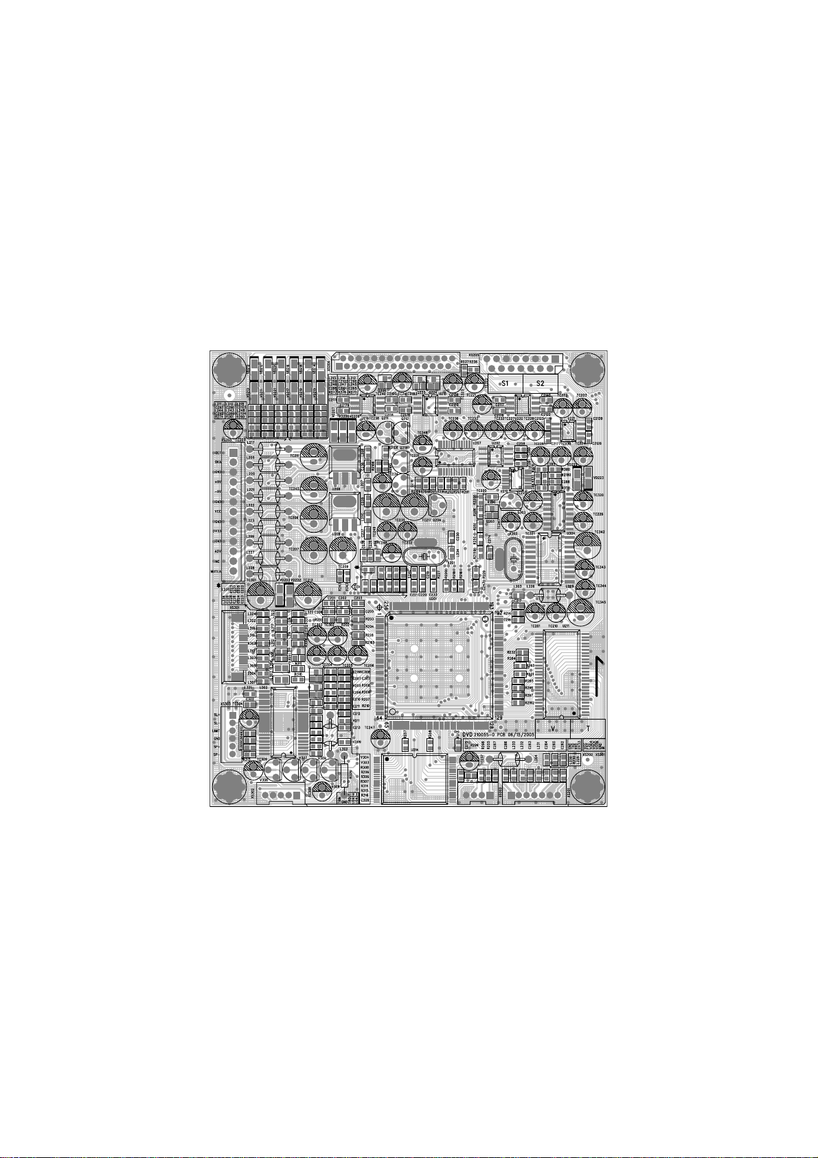
3. Surface layer of MPEG & SERVO Board
- 5 -

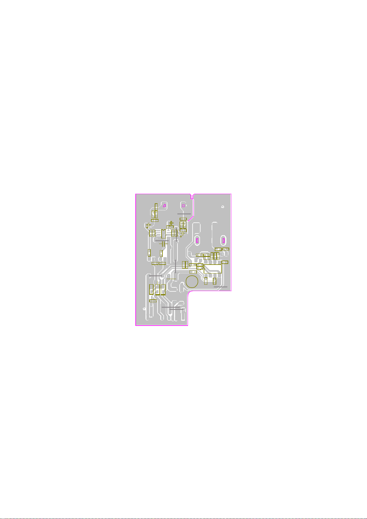
4. Bottom layer of KEY SCAN Board
- 6 -

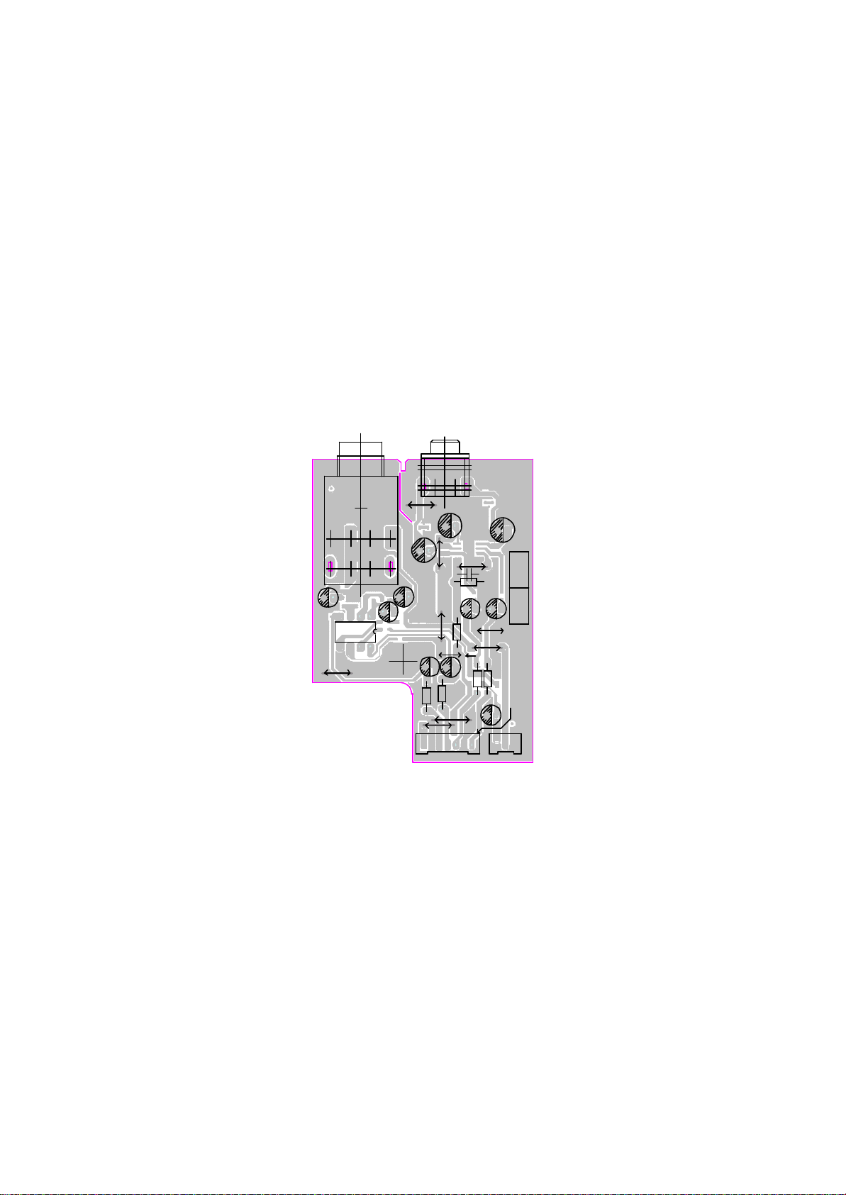
5. Surface layer of AV OUT Board
- 7 -
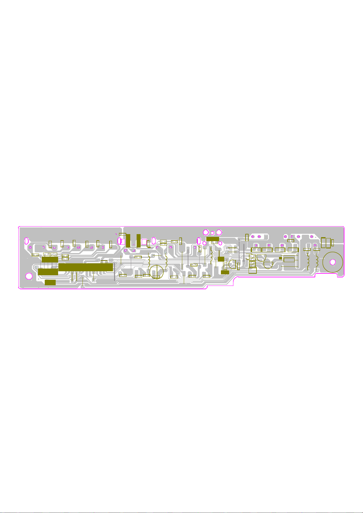
6. Bottom layer of AV OUT Board
L706
L703
L704
C706
C705
L702
L701
C704
C703
C702
C707
C701
C722
R713
L708
C721
C713
R706
C720
L716
L715
C719
L711
R702
C710
L712
C725
D701
D702
R716
C716
C711
C727
C717C718
R715
ZD704
R704
R710
C723
C724
ZD703
ZD702
C728
ZD701
C726
- 8 -
7. Surface layer of MIC Board
MIC601
TC602
69904S-1
DVD 2004/08/20
JP604
JK603
JP609
TC620
JP608
TC619
TC606
JP607
1
TC604
U601
+5V
TC616
R622
AGND
R628
TC615
R621
JP603
XS602
JP606
TC617
JP605
R623
TC611
JP601
JP602
C609
TC621
R629
TC618
DET
R625
+5V
AGNDTL-9V
XS601
JP610
+9V
S
V
AGND
OK
TR
AGND
- 9 -
8. Bottom layer of MIC Board
R630
R634
R626
C613
C610
VD602
U602
R631
C616
VD603
R620
R636
C612
R624
R627
VD601
C611
R632
C615
R635
R617
R615
R633
C608
C614
R611
R618
R619
C606R608
R610
C601
R602L601
C604
R606
R604
C602
1
R616
- 10 -
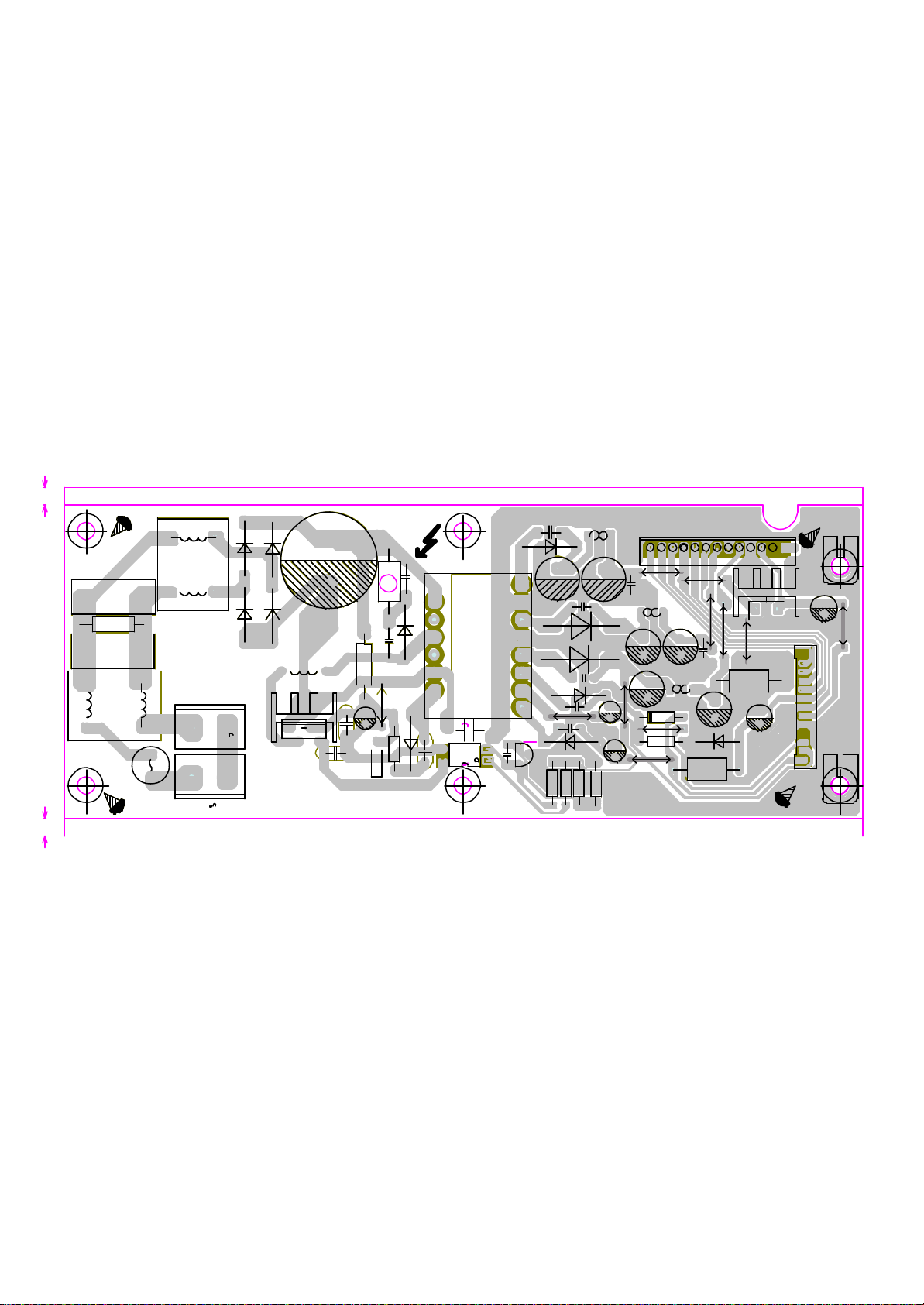
9. POWER Board
4 (mm)
4 (mm)
BC502
R501
BC501
F501
T1.6A 250V
L501
L502
59904S-1
2004/7/5
BCN502
BCN501
D502 D503
D501
LEI
~220V
D504
L503
U501
CAUTION:
FOR CONTIUED PROTECTION
AGAINST
RISK OF FIRE
REPLACE ONLY WITH SAME TYPE F501
T1.6A L250V FUSE
TC501
C506
C504
HIGH
VOLTAGE
R503
R502
TC502
R504
C503
R505
JP501
C502
D505
D506
2
3
4
5
6
7
C505
U502
T501
BC503
C515
U503
D508
C507
16
15
14
13
12
11
10
C513
9
C514
D511
R507
TC503
D510
D509
D512
R506
JP510
R508
L505
TC504
C509
C511
TC511
TC505
TC512
R509
CN502
C508
TC509
JP508
JP507
DETOKAGND
JP502
L507
TC506
L506
ZD501
R510
+9V
JP506
JP505
-9V
JP503
R511
GND
C510
+5V
JP504
TC510
GND
GND
+3.3V
JP509
TC513
ZD502
SA+5V
NC
U504
R512
FL-
-21V
NC
CN501
G502
TC508
NC
DET
OK
AGND
+9V
-9V
GND
SA+5V
GND
NC
FL+
G501
JP511
- 11 -
 Loading...