

Page 1

DV317SI
DV323SIDV324SI
DV326SIDV521SI
servicemanual
Page 2

Catalog
ChapterOneAboutMaintenance
1.1Safetyprecautions
1.1.1Powersupply
1.1.2Precautionsforantistatic
1.1.3Precautionsforlaserhead
1.1.4Aboutplacementposition
1.2Maintenancemethod
1.2.1Visualizedmethod
1.2.2Electricresistancemethod
1.2.3Voltagemethod
1.2.4Currentmethod
1.2.5Cuttingmethod
1.2.6Elementsubstitutionmethod
1.2.7Comparisonmethod
1.3Requireddeviceformaintenance
1
1
1
1
1
2
2
2
2
2
2
2
3
3
3
ChapterTwoFunctionsandOperationInstructions
2.1Features
2.2ControlButtonLocationsandExplanations
2.2.1FrontPanelIllustration
2.2.2RearPanelIIIustration
2.2.3LEDDisplayWindowlllustration
2.2.4RemoteControlIllustration
2.3Accessories
2.4FUNCTIONSETUP
2.4.1FunctionSetup
2.4.2Language
2.4.3Image
2.4.4Sound
2.4.5Playback
4
4
4
4
5
5
5
6
6
6
7
7
8
8
Page 3

2.4.6Karaoke
8
2.4.7Preference
2.4.8Parentalcontrol
2.4.9Initialsetup
2.4.10Resttodefaults
2.4.11Exit
2.5Specifications
ChapterPrincipleandServicing
SectionOnePrincipleofthePlayer
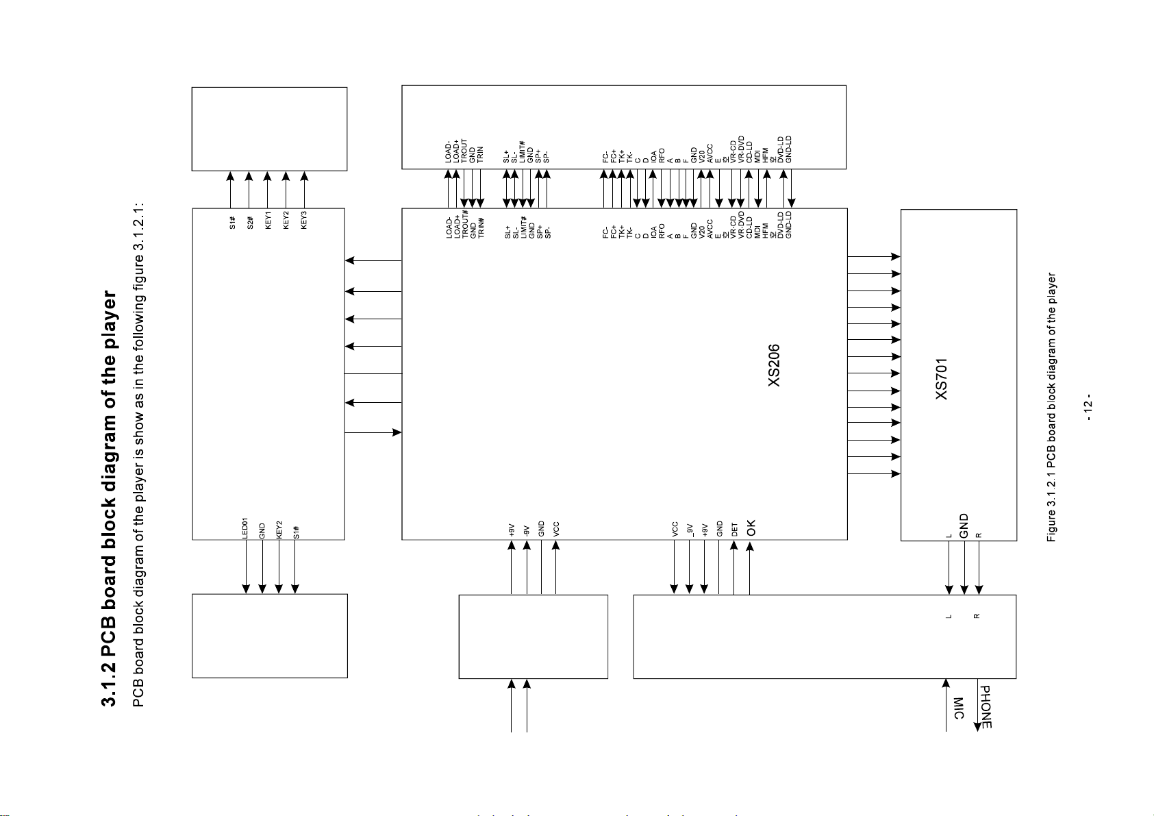
3.1.1Blockdiagramoftheplayer
3.1.2PCBboardblockdiagramoftheplayer
3.1.3HowtouseIC
SectionTwoUnitCircuitPrinciple
3.2.1Introductiontolaserhead
3.2.2Servocircuit
9
9
9
9
10
10
11
11
11
12
13
14
14
16
3.2.3Open/closedrivecircuit
3.2.4Laserpowercontrolcircuit
3.2.5CD/DVDconversioncircuit
3.2.6Mainaxiscontrolcircuit
3.2.7Decodecircuit
3.2.8Resetcircuit
3.2.9Videocircuit
3.2.10Audiocircuit
3.2.11Mutecircuit
3.2.12Decodecircuitvoltageregulating
3.2.13Powercircuit
3.2.14MICcircuit
3.2.15Headphonecircuit
3.1.16AVoutputboardcircuit
3.2.17Controlpanelcircuit
18
18
19
20
21
23
23
24
25
26
27
28
29
29
31
SectionThreeServicingCases
3.3.1Servicingcases
3.3.2Troubleshootingflowchart
SectionFourWaveformdiagram
33
33
39
53
Page 4

SectionFiveFunctionIntroductiontoIC
59
3.5.1functionintroductiontoMT1389E
3.5.2functionintroductionto4558
3.5.3functionintroductiontoAT24C02
3.5.4functionintroductiontoTDA1308
3.5.5functionintroductiontoVIPer22ADIP
3.5.6functionintroductiontoAM5888S
3.5.7functionintroductiontoPT6961(4dv315)
3.5.8FunctionintroductiontoSDRAM
3.5.9FunctionintroductiontoFLASH
3.5.10FunctionintroductiontoLM431A
3.5.11FunctionintroductiontoPc817
ChapterFourDisassemblyandAssemblyProcess
ChapterCinquePCBboard&CircuitDiagram
59
72
73
74
75
76
78
79
80
81
81
83
84
SectionOnePCBboard
SectionTwocircuitdiagram
ChaptersixBOMList
DV323SI/DV324SIServiceManual
7.1.1Features
7.2.1PCBboardblockdiagramoftheplayer
7.3.1MICcircuit(6324SI-1)
7.3.2Headphonecircuit(A323S-0)
7.3.3Controlpanelcircuit
7.3.4Audiocircuit
7.4.1Servicinginstances
7.4.2Troubleshootingflowchart
7.5.1PCBboard
84
92
99
110
110
111
112
112
113
114
115
118
120
7.5.2circuitdiagram
DV326SIServicingManual
8.1.1Features
128
131
131
Page 5

8.2.1PCBboardblockdiagramoftheplayer
132
8.3.1Audiocircuit
8.3.2Controlpanelcircuit
8.3.3MICcircuit(6971S-0)
8.3.4Headphonecircuit(6971S-0)
8.4.1Troubleshootingflowchart
8.5.1PCBboard
8.5.2circuitdiagram
DV521SIServiceManual
9.1.1Blockdiagramoftheplayer
9.2.1PCBboardblockdiagramoftheplayer
9.3.1Audiocircuit
9.3.2MICcircuit(6521SI-1)
9.3.3Controlpanelcircuit
9.3.4Powercircuit
133
134
135
135
137
138
142
144
144
145
146
147
147
148
9.4.1PCBboard
9.4.2circuitdiagram
150
156
Page 6

Chapter One About Maintenance
1.1 Safety precautions
1.1.1 Power supply
When maintenance personnel are repairing DVD players, he should pay special attention to the
power board with 220V AC and 330V DC which will cause hurt and damage to persons!
1.1.2 Precautions for antistatic
Movement and friction will both bring static electricity which causes serious damages to integrated
IC. Though static charge is little, when a limited quantity of electric charge is added to large-
scaleintegrated IC, as the capacitance is very small in the meantime, now the integrated IC is very much
easy to be struck through by static electricity or the performance will decrease. Thus static electricity
prevention is of extraordinary importance. The following are several measures to prevent static
electricity:
1. Use a piece of electric conduction metal with the length of about 2 metres to insert into the earth,
and Fetch the lead wire from the top of the surplus metal and connect to the required static electricity
device. The length and depth of the metal embedded under the earth should be determined according to
the wettability of the local soil. For humid places, it may be shorter, and longer and deeper for dry places.
If possible, it can be distributed and layed in terms of “#” shape.
2. On operating table-board, the antistatic table cushion should be covered and grounded.
3. All devices and equipments should be placed on the antistatic table cushion and grounded.
4. Maintenance personnel should wear antistatic wrist ring which should be grounded.
5. Places around the operating position should also be covered with electric conduction cushion or
Painted with antistatic paint.
1.1.3 Precautions for laser head
1. Do not stare at laser head directly, for laser emission will occur when laser head is working, which
will Hurt your eyes!
2. Do not use wiping water or alcohol to clean laser head, and you may use cotton swab.
- 1 -
Page 7

1.1.4 About placement position
1. Never place DVD player in positions with high temperature and humidity.
2. Avoid placing near high magnetic fields, such as loudspeaker or magnet.
3. Positions for placement should be stable and secure.
1.2 Maintenance method
1.2.1 Visualized method
Directly view whether abnormalities of collision, lack of element, joint welding, shedding welding,
rosin joint, copper foil turning up, lead wire disconnection and elements burning up among pins of
elements appear. Check power supply of the machine and then use hands to touch the casing of part of
elements and check whether they are hot to judge the trouble spot. You should pay more attention when
using this method to check in high voltage parts.
1.2.2 Electric resistance method
Set the multimeter in resistance position and test whether the numerical value of resistance of each
point in the circuit has difference from the normal value to judge the trouble spot. But in the circuit the
tested numerical value of resistance is not accurate, and the tested numerical value of integrated IC's
pins can only be used for reference, so the elements should be broken down for test.
1.2.3 Voltage method
Voltage method is relatively convenient, quick and accurate. Set the multimeter in voltage position
and test power supply voltage of the player and voltage of a certain point to judge the trouble spot
according to the tested voltage variation.
1.2.4 Current method
Set the multimeter in current position and test current of the player of a certain point to judge the
trouble spot. But when testing in current method, the multimeter should be series connected in the
circuit, which makes this method too trivial and troublesome, so it is less frequently used in reality.
1.2.5 Cutting method
Cutting method should be combined with electric resistance method and voltage method to use.
This method is mainly used in phenomena of short circuit and current leakage of the circuit. When
cutting the input terminal voltage of a certain level, if voltage of the player rises again, it means that the
trouble lies in this level.
- 2 -
Page 8

1.2.6 Element substitution method
When some elements cannot be judged good or bad, substitution method may de adopted directly.
1.2.7 Comparison method
A same good PC board is usually used to test the correct voltage and waveform. Compared these
data with those tested through fault PC board, the cause of troubles may be found.
Through the above maintenance method, theoretical knowledge and maintenance experience, all
difficulties and troubles will be readily solved.
1.3 Required device for maintenance
Digital oscillograph ( 100MHE)
TV set
SMD rework station
Multimeter
Soldering iron
Pointed-month pincers
Cutting nippers
Forceps
Electric screw driver
Terminals connecting cord
Headphone
Microphone
- 3 -
Page 9

ChapterTwoFunctionsandOperationInstructions
2.1Features
ThisplayerhasemployedthenewgenerationDVdecodechipwithbuilt-inDolbyDigitaldecoder
whichwillbringyoutoabrand-newAVentertainmentworld.The2-lasersupererror-correction
mechanismsupportsCD-R.
Brand-newAVEffects
1.CompatiblewithMPEG4discstoproducewonderfulpictures.
2.108MHz/12bitvideoDAC,withmorevividandbrilliantpictures.
3.Progressive-scanvideooutputstoeliminatetheflickershardlyovercomebyinterlacingscanand
thereforeyoureyesightwillbewell-protected.Atthesametime,thepicturesdefinitionIssharply
enhancedandthepictureswillbefiner,smootherandstabler
4.Brightness,chromaandcontrastadjustmentfunctionstorenderyoureyesmorecomfortable.
5.DigitalechoKaraoketoenableyoursingingeasier.
6.CompositeVideo,S-VideoandComponentVideooutputs.
7.Dolbyoutputfor2channel(DOWNMIX)
HighQualityDigitalAudio
1.OpticalandcoaxialoutputsforDigitalaudio.
2.DTS,DolbyDigital,PCMDigitalaudiooutputstosatisfytheFans’sacousticrequirements.
ManyConvenientFeatures
1.ScreensaverprotectsyourTVsetcarefully.
2.ThenovelMp3playbackwindowGUIprovidesyouanewwaytoappreciateMp3music.
3.Multi-angleplaybackfunctionmakesitpossibleforyoutoviewascenefromdifferentcamera
angles.
4.It’spossibletoselectthedesiredbeginning,developmentandendingofastory.
5.Directentryintodesiredscenes(title/chapter/tracksearch).
6.Zoomingfunctiontozoomupanyplayingpicture.
7.CapableofplayingPAL/NTSCdiscs.
8.MultipleaspectratiostofitTVsetsofvariousscreenratios.
9.Parentallockfunctiontopreventchildrenfromwatchingunsuitablediscs.
10.Multipledubbinglanguagesandsubtitlelanguagesbringyouthebestentertainmentstatusall
thetime.
SuperCompatibilitywithsuperVCD,VCD,CD ,CD-R,MP3,HDCD,KODAKPICTURECDetc.
2.2ControlButtonLocationsandExplanations
2.2.1FrontPanelIllustration
1
10
-4-
324
6 7 8 95
Page 10
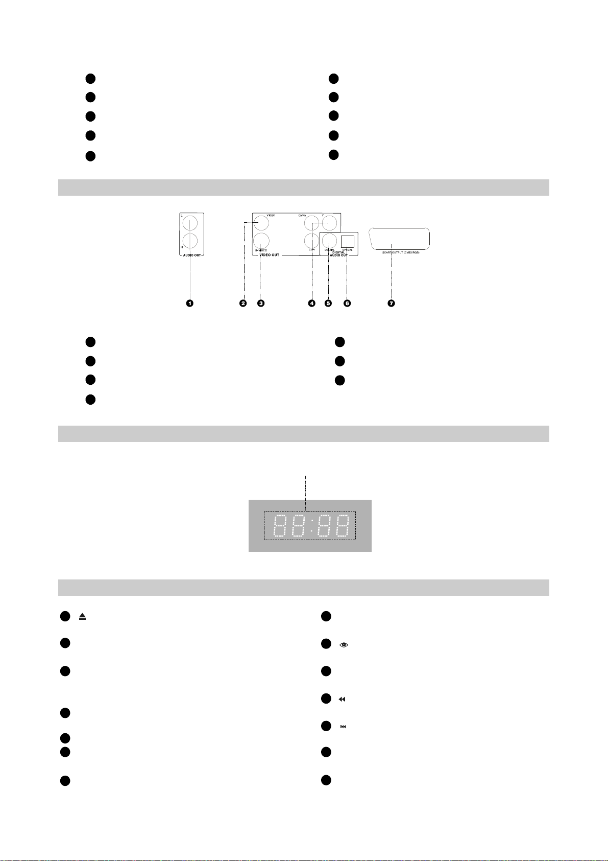
1
POWERswitch
2
Displaywindow
3
IRSENSOR
4
MICjack
5
Headphonejack
2.2.2RearPanelIIIustration
6
STOPbutton
7
PLAYbutton
8
PAUSEbutton
9
OPEN/CLOSEbutton
10
Disctray
1
2CHAudioOutjacks
2
VideoOutjack
3
S-Video
4
VideoComponent/YPbPrOutjacks
2.2.3LEDDisplayWindowlllustration
2.2.4RemoteControlIllustration
1
[]
Button
Openorclosethedisctray.
2
LANGButton
Changetheaudiolanguageoraudiochannel.
3
MEMORYButton
Savetheplayingpointorjumptothesaved
point.
4
DISPButton
Displayorhidediscinformation.
5
NUMBERButtons
6
BROWSEButtons
switchnewuserinterface.
7
CURSORButtons
Playbacktime
8
9
10
11
12
13
14
5
DigitalAudioCoaxialOutjack
6
DigitalAudioOpticalOutjack
7
SCARTOutjack
SETUPButton
FunctionSetup.
[]
Button
Open/closethevirtualkeyboardfunction.
KARAOKEButton
Karaokeoperationmenu.
[]
Button
Fastbackwardplay.
[]
Button
Skipbackward.
PEPEATButton
Repeatplay.
A-BButton
-5-
Page 11
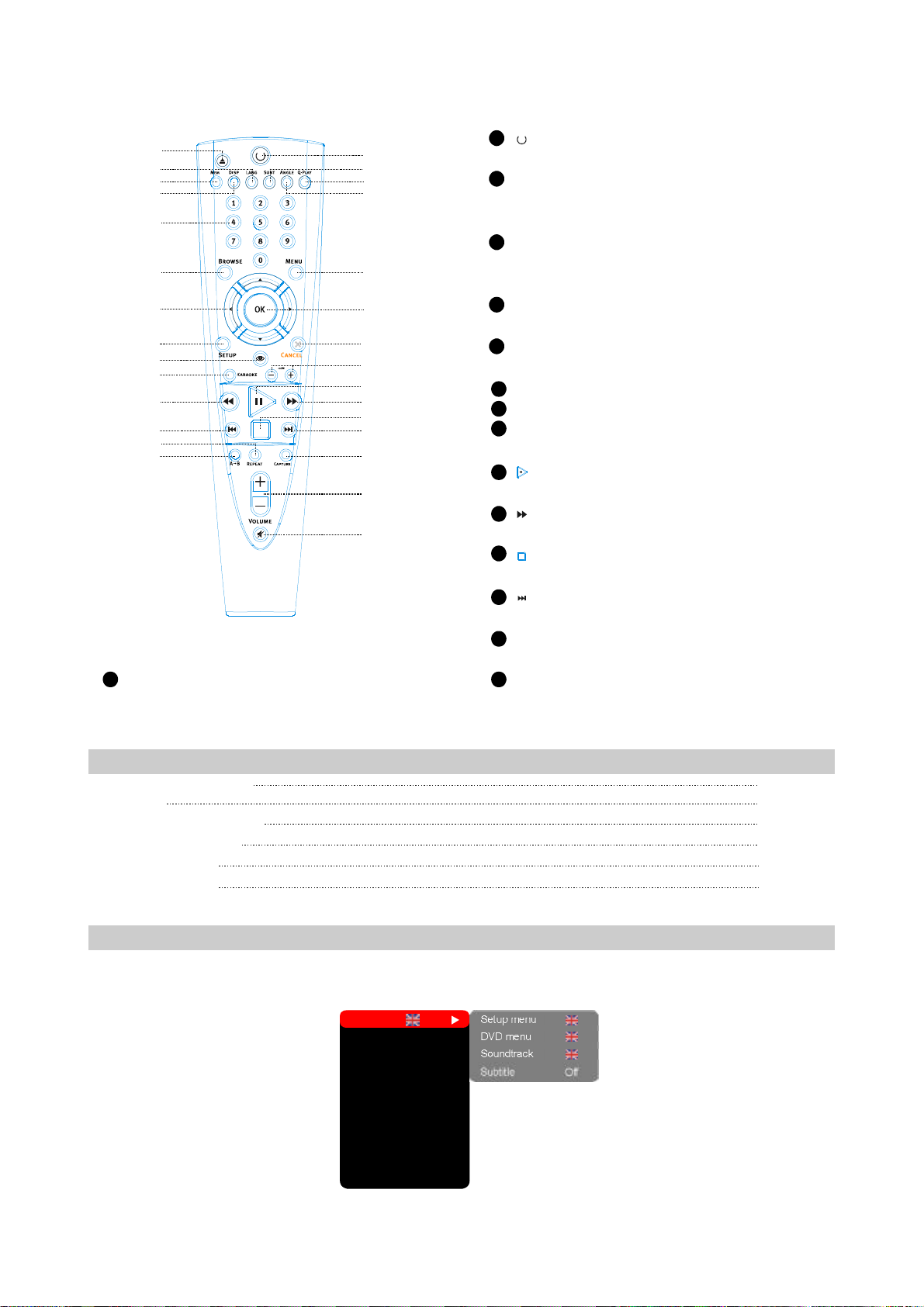
10
12
13
14
1
2
3
4
5
6
7
8
9
11
15
16
17
18
19
20
22
23
24
25
26
27
28
29
21
MUTEButton
Pressoncetomute,twicetoturnoff.
Repeattheselect.
15
[]
Button
Pressoncetostandby,Presstwicetoplay.
16
SUBTButton
Changesubtitlelanguage,SwitchJPEG
displaymode.
17
Q-PLAYButton
Skiptheadvertisement/warningandplaythe
DVDdirectly.
18
ANGLEButton
Changecameraangle.
19
MENUButton
DisplayDVDmenuoropen/closePBC.
20
OKButton
21
CancelButton
22
ZOOM+/-Button
Zoomin/outthedisplayedframe.
[]
23
Button
Playorpauseplayback.
[]
24
Button
Fastforwardplay.
25
[]
Button
Stopplayback.
26
[]
Button
Skipforward.
27
CAPTUREButton
Settheplayedimageasthepower-onlogo.
2829
VOL+/-Button
Increase/decreasevolumelevel.
2.3Accessories
AUDIO/VIDEOCORD
REMOTE
AAASITEBUTTERIES
WARRANTYCARD
USERMANUAL
2.4FUNCTIONSETUP
2.4.1FunctionSetup
1.Pressthe[SETUP]buttonandthescreendisplaystheselectionmenuoffunctionsetup.
Language
Image
Sound
Playback
Karaoke
Preference
Parentalcontrol
Initialsetup
Resettodefaults
Exit
Setupmenu
DVDmenu
Soundtrack
Subtitle
Off
1PCS
1PCS
2PCS
1PCS
1PCS
1PCS
-6-
Page 12

2.Pressthe[CURSOR]buttontoselectthemenu
tobeenteredandpressthe[OK]orbuttonto
confirm.Orpressthe[CURSOR]buttonto
Exititemandthenpressthe[OK]buttontoexit
3.Press[UP/DOWN]arrowtoselectthedesired
itemyouwanttosetandpress[OK].
Forexample,press[UP/DOWN]arrowstoselect
IMAGEandpress[OK].TheImagesettingpage
Appearsonthescreen.
Off
LB
AUTO
PAL
IS
NTSC
L.
0
0
0
0
TVsystem
TVscanmode
Videoout.
TV
format
Sharpness
Gamma
Brightness
Contrast
Hue
Saturation
AUTO
S-Vid.
menulangwhenplaying.
Optionalsetting:
◆
Russian,English,Estonian,
Latvian,Kazakh,Romanian,Byelorussian,
Ukrainian,Chinese,Others.
Default:English.
◆
3.Sountrack:Tosetthepreferenceaudio
languagewhenplaying.
Optionalsetting:
◆
Russian,English,Estonian,
Latvian,Kazakh,Romanian,Byelorussian,
Ukrainian,Chinese,Others.
Default:English.
◆
4.Subtitles:Tosetthepreferencesubtitle
languagewhenplaying.
Optionalsetting:Off,
◆
Russian,English,
Estonian,Latvian,Kazakh,Romanian,
Byelorussian,Ukrainian,Chinese,Others.
Default:Off.
◆
2.4.3Image
4.Press[UP/DOWN]arrowtoselectthe
SHARPNESSitem.Press[OK]toconfirmit.
Andthenpress[UP/DOWN]arrowtoselectthe
desiredvalus.Forexample:Press[UP/DOWN]
arrowtoselect“Medium”,thenpress[OK],the
TVscreendisplay.
TVsystem
TVscanmode
Videoout.
TV
format
Sharpness
Gamma
Brightness
Contrast
Hue
Saturation
AUTO
Com.
LB
Off
IS
L.
High
Medium
0
Low
0
0
0
5.Press[LEFT]buttonifyouwanttoreturntothe
previoussetuppage.
6.Press[SETUP]toexitthesetupmenu.
2.4.2Language
Setupmenu
DVDmenu
Soundtrack
Sbutitles Off
1.Setupmenu:Thisitemisusedtosetthe
promptslanguageonthescreen.
Optionalsetting:Russian,English,Ukrainian.
◆
Default:English.
◆
2.DVDmenu:Tosetthepreferencedisc
Russian
English
Ukrainian
Off
AUTO
PAL
IS
NTSC
LB
L.
0
0
0
0
TVsystem
TVscanmode
Videoout.
TV
format
Sharpness
Gamma
Brightness
Contrast
Hue
Saturation
AUTO
Com.
1.TVsystem:Thisitemisusedtothevideo
outputsystemofthisunit.
Optionalsetting:Auto,PAL,NTSC.
◆
Default:AUTO.
◆
2.TVscanmode:Toset
Interlacedscanmode
Optionalsettings:Progressive,Interlaced.
◆
Default:Interlaced
◆
Progressivescan,
.
3.Videooutput:TosetthetypesofSCARTout
connector.
4.TVnformat:Tosettheaspectratioofthis
player’soutputimage.
Optionalsetting:4:3Pan-scan,16:9letterb.,
◆
16:9TV.
Default:16:9letterb
◆
5.Sharpness:Usedtosetthesharpnessof
videooutputs.
Optionalsetting:High,Medium,Low.
◆
Default:Medium.
◆
6.Gammaemendation:Thisitemisusedtosetup
theGammavalueofvideooutput.
Optionalsetting:High,Medium,Low,Off.
◆
Default:Off.
◆
-7-
Page 13

7.Brightness:Usedtosetthebrightnessofvideo
outputs.
8.Contrast:Usedtosetthecontrastofvideo
outputs.
9.Hue:Usedtosetthehueofvideooutputs.
10.
Saturation:Usedtosetthesaturationof
videooutputs.
Brightness,contrast,hueandsaturation
◆
adjustingmeans:
A.
Press[UP/DOWN]arrowinthevideosetup
menutoselectthedesireditemyouwantto
adjust.Press[OK]or[RIGHT]buttontoenter
Theitem'sadjustment.
B.
Press[UP/DOWN]arrowtoadjustthesetting
Value.
2.4.4
Sound
Mixer...
Digitaloutput
Tuning
Stereomix
Surr.Mix
L+R
off
1.Mixer...
Stereomix
Surr.Mix
L+R
L+R
L
off
R
A.Stereomix:Tosettheoutputmeansoftheleft
orrightaudiowhenplayingaDolbydiscwith
separatetwo-channelaudio.
Optionalsetting:L+R,L,R.
◆
Default:L+R.
◆
B.Surr.Mix:Tosetoutputmeansofthesurround
leftandrightaudiowhenplayingastereodisc.
Optionalsetting:Off,sum,Virt.Surr.
◆
Default:Off.
◆
2.Digitaloutput:selecttosettheformatand
streamformofdigitalaudiooutput.
A.SPDIFformat:
Optionalsetting:RAWformat,SPDIF/PCM.
◆
Default:RAWformat.
◆
B.LPCM
Optionalsetting:48kHz16bit,96kHz24bit.
◆
Default:48kHz16bit.
◆
3.Tuning:
A.Maxvolume:setthemaximumvolumelimit.
B.Equalizer:TosetEqualizermodes.
Optionalsetting:Off,Rock,Pop,Live,Dance,
◆
Techno,Classic,Soft.
Default:Off.
◆
C.Echo:Tosetdifferentsoundfieldeffects.
Optionalsetting:Off,Concert,Livingroom,
◆
Hall,Bathroom,Cave,Arena,Church.
◆Default:Off.
D.Tonebalance
:tosetthetoneleveltomatch
yourdiapasonwhenyou'resinging
Methodtoadjusttonecontrol:
◆
Press[UP/DOWN]cursorbuttonstoselect
◆
"tone"iteminAudioSettingpage,andthen
press[OK]or[RIGHT]buttontoenter
AdjustmentMenu.
b.Press[UP/DOWN]cursorbuttontoadjust
settingvalue.
C.Press[OK]or[LEFT]buttontoreturntoAudio
Settingpageafteradjustmentsaredone.
2.4.5Playback
DVD
VCD/SVCD
Files
Repeat
Loadeffect
A.P.V
1.DVD:setwhetherinformationof
advertisementandwarningsatthebeginning
ofDVDdiscisskippedtoplaythemovie
directly.
Optionalsetting:Yes,NO
◆
Default:number
◆
Optionalsetting:On,Off.
◆
Default:On.
◆
2.VCD/SVCD:TosetthePCBstatus.
WhenplayingSuperVCDorVCD2.0discs,if
◆
thePCBisON,themenuimagedisplays.
3.Files:datadiscmayprobablyincludesMp3,
JPEGandMPGformatfilesinwhichyoumay
selectDVDplayertoreadthefiletype.
Optionalsetting:Audio,Picture,Video.
◆
Default:Audio,Picture,Video.
◆
4.Repeat:selecttherepeatplaybackmode.
Optionalsetting:Off,Single,all.
◆
Default:Off.
◆
5.Loadeffect:setthemaytoplayJPEGimage.
Optionalsetting:Off,fromtop,frombottom.
◆
Default:Off.
◆
Advertisemenu No
Off
Off
2.4.6Karaoke
Microphone
Volume
Echo
1.Microphone:switchonoroffmicrophone.
Optionalsetting:On,Off.
◆
Default:Off
◆
2.Volume:.
On
4
4
-8-
Page 14

A.Inmicrophonesetuppage,press[UP/DOWN]
cursortoselect“Volume”item,andthenpress
[OK]buttontoentertheadjustmentmenu.
B.Press[UP/DOWN]cursortoadjustthesetup
value.
C.Afteradjustmentfinishes,press[OK]button
toreturntomicrophonesetuppage.
Microphone
Volume
Echo
Off
On
Off
5
5
3.Echo:
A.Inmicrophonesetuppage,press[UP/DOWN]
cursortoselect“Echo”item,andthenpress
[OK]buttontoentertheadjustmentmenu.
B.Press[UP/DOWN]cursortoadjustthesetup
value.
C.Aftertheadjustmentfinishes,press[OK]
buttontoreturntomicrophonesetuppage.
Microphone
Volume
Echo
On
4
◆Default:On.
2.4.8Parentalcontrol
any
Kid
G
Allowed..
Setpassword
Any
1.Allowed..:Tosettheparentalcontrolratingsto
preventchildrenfromwatchingtherestricted
contents.(Incasethediscsupportsthis
function.)
Optionalsetting:any,Kid,G,PG,PG-13,PGR,
◆
R,NC-17.
Default:any.
◆
2.Setpassword:Tosetfourdigitpasswordto
enableyoutochangetheparentalcontrol
ratings.
Default:7890.
◆
Oldpassword
PG
PG-13
PGR
R
NC-17
2.4.7Preference
std.
On
Off
On
Off
Gr.equalizer
Background
Screensaver
1.Gr.equalizer:Thisitemisusedtosetwether
theDynamicSpectrumisallowed.
Optionalsetting:On,Off.
◆
Default:Off.
◆
DynamicSpectrumdisplayisinvalidinData
◆
discDVDAUDIOplayback.
、
2.Background:Thisitemisusedtisetupthesort
ofPower-inLogo.
Optionalsetting:Standard,saved.
◆
Default:Standard.
◆
NOTE
TheScreenLogorefersthatusetheimage
selectedbypressingthe[CAPTURE]buttonas
thepower-onlogo.Whenintheoperationof
changingscreen,ifthepower-onlogohasnot
setinScreenLogo,theunitwillautomaticallyset
thepower-onlogoasScreenLogo.
3.Screensaver: Openorclosethescreensaver
function.
Optionalsetting:On,Off.
◆
Newpassword
Verify
OK Cancel
2.4.9Initialsetup
Auto
PAL
NTSC
Press[UP/DOWN]arrowtoselectthedesired
optionandPress[OK]buttontoconfirmit.
NOTE
Inthissetupstate,youmaynotpress[LEFT]
buttontoreturntothepreviousmenu.
2.4.10Resttodefaults
Loadfactorysettings
OK
Cancel
-9-
Page 15
Resettodefaults:Torestoreallsettingstothedefaultvalueexceptfortheparentalcontroland
passwordsettings.
2.4.11Exit
Language
Image
Sound
Playback
Karaoke
Preference
Parentalcontrol
Initialsetup
Resettodefaults
Exit
Press[UP/DOWN]arrowtoselecttheExititem.Press[OK]buttontoexitthesetupmenu.
2.5Specifications
Playable discs
Inputs
Outputs
Video characteristics
Audio characteristics
Operating voltage
Power consumption
General specification
Operating temperature
DVD-Video,Super VCD,VCD,MPEG-4,CD-DA,CD+G,HDCD,MP3,WMA,
Kodak Picture CD,JPEG
MIC input
Audio outputs
Video outputs
Analog audio output: Stereo
Digital audio output: Coaxial,Optrcal
Composite,S-Video,componont Y Cb Cr, progressive
scan output Y Pb Pr,RGB/SCART
Headphones output
Video amplitude: 1.0Vp-p(75Ω)
S-Video amplitude: Y:1.0Vp-p(75Ω) C:0.286Vp-p(75Ω)
Component video amplitude: 1.0Vp-p(75Ω)
Cb/Cr:0.7Vp-p(75Ω)
Frequency response 20-20000 Hz(±1 dB)
Signal-to-noise ratio >100(dB)
THD <0.01%
~110-250V,50/60 Hz
14W
Dimensions: 380×210×43 mm
Mass: 1.85 kg
5-35℃
Operating humidity
◆
Designandspecificationsaresubjecttochangewithoutnotice.
◆
Wedonotgraranteethatalldiscscanbeplayedsmoothlyduetothediscquality,discrecording
qualityandrecordingformat.
15-75%(no condensation)
-10-
Page 16
ChapterPrincipleandServicing
SectionOnePrincipleofthePlayer
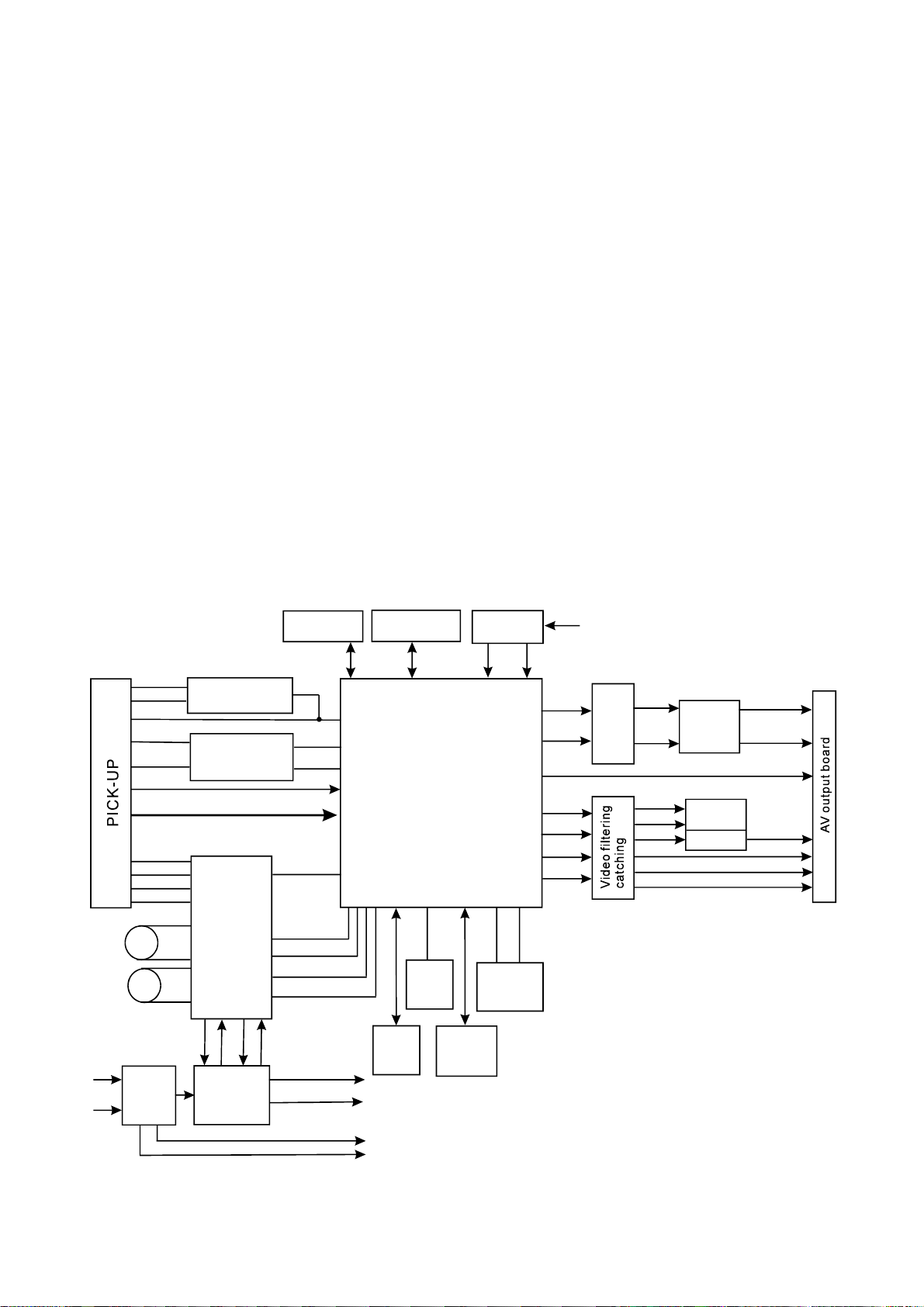
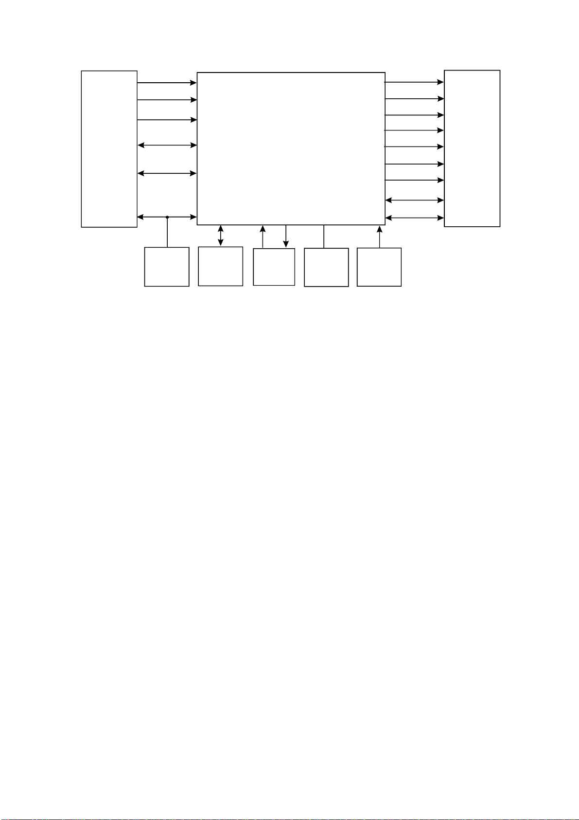
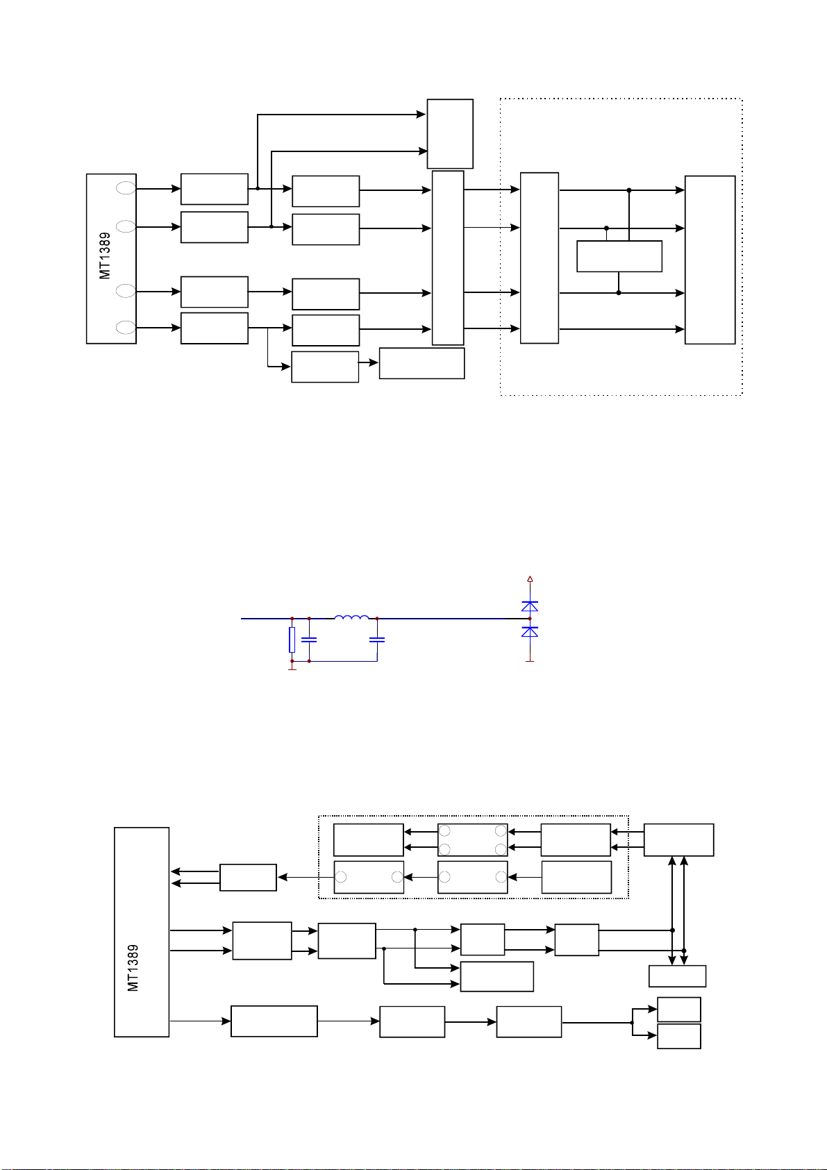
3.1.1Blockdiagramoftheplayer
DV317SIiscomposedbydecodecircuit,servocircuit,audiocircuit,videocircuit,MICcircuitand
powercircuit,theblockdiagramoftheplayerisshownasinthefollowingfigure3.1.1.1:
Feed
electric
machine
Main
axis
electric
machine
ACIN
VR-DVD
VD-CD
LD-DVD
LD-CD
TKTK+
FC+
FC-
SL+
M
M
SL-
SP+
M
SP-
Power
board
CD/DVDswitch
Laserpower
control
DVD:A/B/C/D/RFO
CD:A/B/C/D/E/FRFO
Am5888
U301
TRB2
TRB1
REGO1
Voltage
regulating
circuit
SDRAM64M
U208
Ld02
Ld01
MDI
VIP4
FOSO
FMSO
DMSO
TRSO
REGO2
V18
Dv33
+9V
IOA
FLASH16M
U207
MT1389E
U201
UREST
Reset
Panel
MICboard
XI
SDA
SCL
27Mclock
EEPROM
U202
24C02
XO
MIC1
AL
AR
CVBS
Y/G
CB/B
CR/R
Audio
amplifying
filtering
U209
CVBS
B/U
R/V
G/Y
L
R
SY
SC
Audio
output
terminal
S-video
Videooutput
L#
R#
SPDIF
VIEDO#
PB#
PR#
Y#
-9V
Figure3.1.1.1Blockdiagramoftheplayer
-11-
Page 17
Buttonboard
A983E-0
Loaderframe Smallbracket
Laserhead
XS403
Mainpanel
4983e-1
XS402
1
234
Subsidiarypanel
9DV983-0
7
6
5
4
3
2
1
XS307 Xs306 XS301
FSO
VSDA
VSCK
VSTB
GND
Xs201
Decodeboard
2DV983A-2
VCC
IR
XS203
CN501
Powerboard
XS205
XS601
MICandheadphoneboard
5317SI-1
HSYNC#
VSYNC#
SPDIF
VCC
VIDEO_R/V
GND
VIDEO_G/Y
GND
VIDEO_B/A
POATO
VIDEO#
+9V
L#
R#
6DV317SI-0
1
2
3
4
5
6
7
8
9
10
11
12
13
14
PDAT2
PDAT1
SPDIF
VCC
Pr
VGND
Y1
VGND
Pb
PDATO
VIDEO#
+10V
L
R
AVboard
7231-0
XS702
XS602
BCN501
AC220V
Page 18

Thismachineismainlycomposedofdecodeboard,powerboard,AVoutputboard,MIC&
headphoneboard,mainpanel,subsidiaryboardandbuttonboard.
Decodeboard:includesdecode,servo,audio,videooutputcircuit.
Powerboard:providesworkingvoltageforeachcircuit,outputvoltagehas+9V,9Vand+5V.
AVoutputboard:includesSCART,componentvideo,opticalandcoaxialoutputterminal.
MIC&headphoneboard:withsingle-waymicrophoneinput,headphoneamplifyingandoutput
function.
Mainpanel:connectedwithsubsidiaryboard,buttonsboardtofulfilbuttonsfunctioncontrol,remote
controlandLEDdisplay.
Remark:inordertofacilitatereaderstobetterknowthecompositionofmachine,wehavemade
PCBcompositionfigure,theconnectinglinesinPCBcompositionfigurearethemaincontrolline,signal
lineandpowercordconnectedthroughflatcable,butallconnectedflatcablearenotincluded.
3.1.3HowtouseIC
DV317SIICusageinstructionisshownasinthefollowingtable:
Semi-finished PCB
name
Power board
5317SI-1
Main panel 4983E-1
OK board
6DV317SI-1
Decode board
2983A-2
IC model name Location Function
AZ431 U503 Precise voltage regulator
PC817 U502 Photoelectric coupler
FSDH321 U501 Power switch IC
PT6961 U401 Control panel IC
HS0038B3V U402 Remote control receiver
KA4558 U603
TDA1308 U604 Headphone amplifying
NJM4558 U209
HY57V641620HGT-7 U208 SDRAM
24C02 U202 EEPROM
MT1389 E version U201 Decode chip
AM5888S U301 Servo drive
29LV160BE U214 FLASH
Operational amplifier (MIC
amplifying)
Operational amplifier (audio
amplifying)
-13-
Page 19
SectionTwoUnitCircuitPrinciple
3.2.1Introductiontolaserhead
1.Functionintroductiontolaserheadflatcableisshownasthefollowingtable:
Pin Name
1 F- Input loader 2.52 2.34 0.46
2 F+ Input loader 2.49 2.49 0.93
3 T+ Input loader 2.53 2.51 0.94
4 T- Input loader 2.58 2.51 0.93
5 C Input MT1389 2.2 2.25 2.04 Disc data signal
6 D Input MT1389 2.2 3.2 2.04 Disc data signal
7 IOA Input MT1389 0.01 3.2 3.21
8 RF Input MT1389 2.21 2.53 1.28 The sum of disc data signal
9 A Input MT1389 2.17 2.22 2.04 Disc data signal
10 B Input MT1389 2.19 2.27 2.04 Disc data signal
11 F Input MT1389 2.07 2.44 2.03 Supplementary signal used in trace
12 GND Ground 0.01 0.01 0 Grounding
13 V20 Input loader 2.04 2.06 2.03 Reference voltage
Signal flow
direction
DVD disc CD disc No disc Function description
Focus error signal is added to two sides of
pick-up focus coil
Trace error signal is added to two sides of
pick-up trace coil
Disc identification signal, CD is 3.3V, DVD
is 0V
14 Vcc Input loader 5.04 5.04 5.02 Supply voltage for loader
15 E Input MT1389 2.06 2.45 2.03 Disc data signal
16 Blanking haning in air 0.01 0 0 unused
17 VR-CD Input loader 0.21 0.01 0
18 VR-DVD Input loader 0.01 0.2 0
19 LD-CD Input loader 0.09 2.1 0 CD laser power control signal
20 MDII Input MT1389 0.21 0.2 0 CD and DVD laser power monitoring signal
-14-
Through the handling inside loader, make
sure MD11 is 180mV when reading CD
Through the handling inside loader, make
sure MD11 is 180mV when reading DVD
Page 20

Pin Name
21 HFM Input loader 5.04 5.04 5.02
22 Blanking unused 0.01 0.1 0
23 LD-DVD Input loader 2.21 0.1 0 DVD laser power control signal
24 GND unused 0.01 0.01 0 Grounding
Signal flow
direction
DVD disc CD disc No disc Function description
High frequency overlapping signal produces
laser with different wave length inside
loader
Note:1.WhenreadingDVD,thereareonlyA,B,C,Dsignals.
2.WhenreadingCD,thereareA,B,C,D,E,Fsignals.
3.RFO=A+B+C+D.
4.Focuserrorsignal=(A+C)-(B+D)Traceerrorsignal=E-F.
2.Workingprinciple
(1)Lasertube:wavelengthofloaderDVDlaserdiodeis650nm,wavelengthofCDlaserdiodeis
790nm,thewavelengthwhichiswithin370nmand750nmisvisiblelight,thelaserinthecourseof
readingDVDdiscisvisiblelight,andthatwhenreadingCDdiscisinfraredlight.
(2)Principleaboutlaserheadpicksupsignal:laserbeamprojectsontodisc,whenlaserbeam
focusprojectsontodiscvertically,laserbeamwillproducereflection,reachonlightsensorthrough
reflectionloopandconverseintoelectronicsignalthroughphotoelectriccell.Forthereflectionloop
producedinnonpitinformationareaandpitinformationareaindischasdifferenceandreflectsinto
differentpositionoflightsensor,photoelectricdiodeindifferentpositionsonlightsensorwillproduce
differentsignalstoprocessallsignalsonlightsensorandthenproducedigitalsignals.
(3)Focus,tracecoil:whenlaserheadisreadingsignalsnormally,informationsideshouldbeinthe
focusoflaserbeam,becauseoffactorsofdiscerror,highspeedrotationandmachineerror,itis
unavoidablethatlaserbeamfocusdeviatesfrominformationfacetoproducephenomenaoforbitboas
andrefocusing.Focus,tracecoilisaddedonloadertoadjustlaserbeamtomakeitcorrectlyfocusin
informationarea.
(4)FormationofRsignal:whendiscreadingisnormal,lightsensorwillhave160MV,vagueand
eyepatternwaveformwhichisaddedonA,B,C,Drespectively,andoutputRsignalfromFROpin
F
F
afterbeingoverlappedbyadderinsidelightsensor,thefrequencywhenreadingDVDdiscismuch
higherthanthatwhenreadingCDdisc,outputamplitudeisabout1.4V.
-15-
Page 21
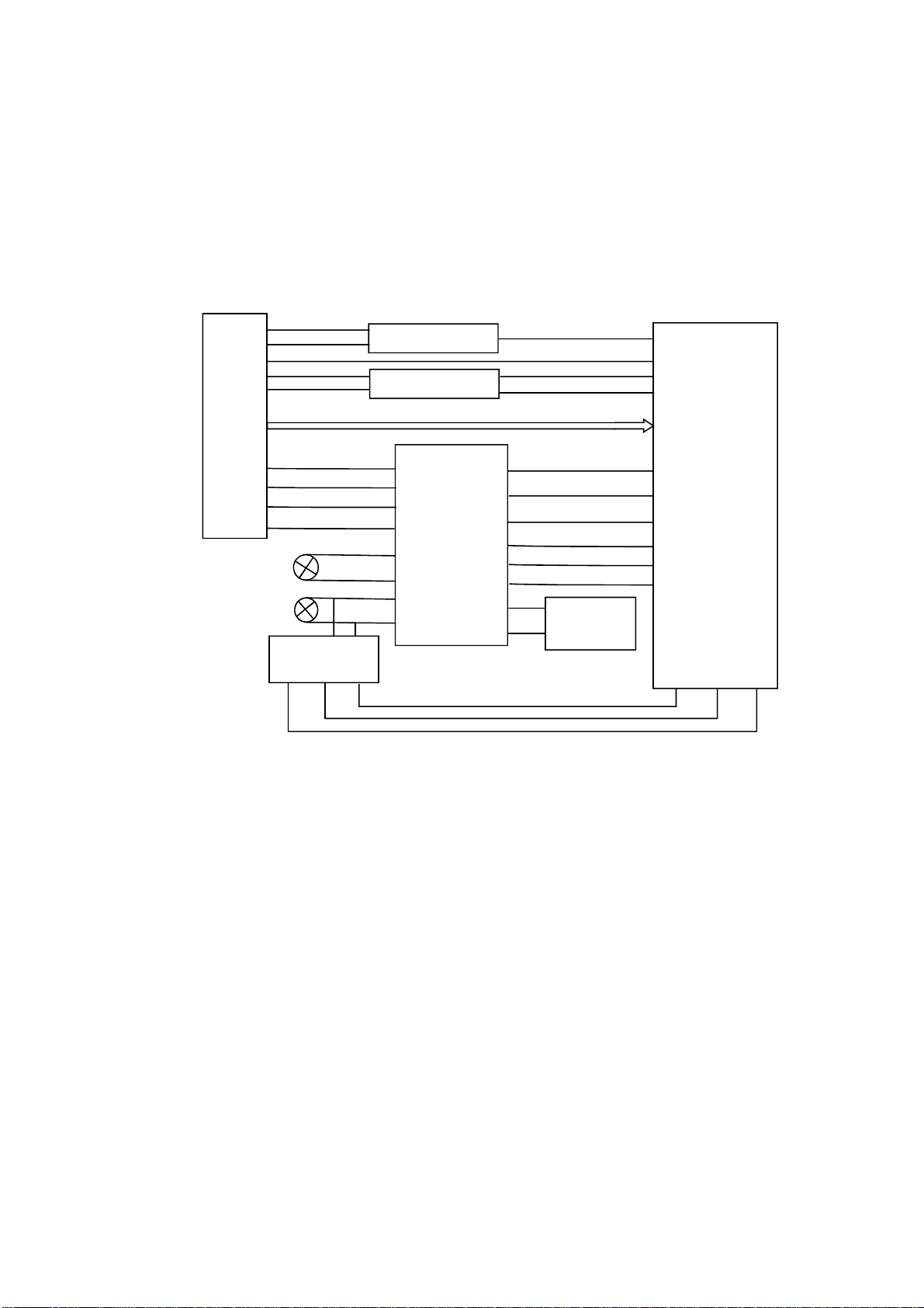
3.2.2Servocircuit
1.ServosystemofthisplayeradoptsSANYOloader+MTKdecodesolution(MT1389E+FLASH
(16M)+SDRAM(64M)),anditsservocircuitismainlycomposedoffrontendsignalprocessing,digital
servoprocessing,digitalsignalprocessingICMT1389EanddrivecircuitAM5888S,inwhichMT1389E
isalsothemaincomposedpartofdecodecircuit.Servocircuitblockdiagramisshownasinthe
followingfigure
Feedelectricmachine
Mainaxiselectricmachine
3.2.2.1:
Xs301
ABCDEFRFO
Mainaxiscontrol
detectcircuit
Switchcircuit
APCcircuit
TK-15
TK+16
FC+14
FC-13
SL+17
SL-18
SP-12
SP+11
Am5888
LOAD+
LOAD-
23
26
4
7
1
6
FOSO
FMSO
TRSO
DMSO
TRCLOSE
TROPEN
10
Discin/out
9
electricmachine
IOA
MD11
LDO2
LDO2
MT1389
U201
Figure3.2.2.1Servocircuitblockdiagram
2.Workingprinciple
Afterpoweronordiscintoproperposition(onloaderframeforgeneralDVDplayers,onPCBboard
belowdoorforPDVDplayers),loaderlaserheadbeginsreset,afterlaserheadreachestoproper
position,detectswitchwillgiveasignaltoMT1389,MT1389beginstooutputfocus,mainaxisandlight
emissionsignals,discbeginstorotate,laserheadbeginstorecognizediscinformationandjudge
whetherdiscisCDorDVDaccordingtodiscinformationtofacilitatetooutputlevelfromIOApin,control
discswitchcircuitandlaserheadPDICtomakecorrespondingacts.Atthesametime,MT1389also
adjustslaserpoweroutputthroughlaserpowercontrolcircuit.
Afterloaderreadsdiscinformation,A,B,C,D,EandFsignalareformedthroughphotoelectric
conversiontoMT1389(DVDonlyhasA,B,C,Dsignals)andR
MT1389MT1389
ofrespectively,afteramplifyingprocessingofpre-amplifierinside,nowsignalsare
dividedinto2waysinside:onepart,throughsummationamplifyingandsubtractioncircuit
inside,producesservoerrorsignal,afterdigitalservosignalcircuitprocessing,forms
MT1389
MT1389
Fsignalandoutputfrompin2~11,18,19
-16-
Page 22

Correspondingservocontrolsignals,outputsFOO,TRO,DMOandFMSOservocontrolsignalfrompin
42,41,37and38ofrespectivelyandthensendtoservodrivecircuitfordriveamplifying
MT1389
throughtheintegrationcircuitcomposedbyresistorandcapacitorandbringalongfocuscoil,tracecoil,
mainaxiselectricmachineandfeedelectricmachineafterdriveamplifying.
Amongthese,focusand
traceservoareusedtocorrectobjectivepositionaccurately;feedservoisusedtobringalonglaser
headtomakeradiallarge-scalemovewhichbelongstothepreliminaryadjustmenttolaserheadposition;
andmainaxisservoisusedtocontrolmainaxiselectricmachinetomakeitreadsignalsinmeansof
constantlinearvelocityandbringalongdisctorotate.AfterprocessingofamplificationbyVGAvoltage
controlamplifierandequalizationfrequencycompensationinsideMT1389,anotherpartofsignalsare
changedintodigitalsignalsthroughinternal A/Dconverter.WhenloaderisreadingCD/VCDsignals,
thesesignalsareconductedEFMdemodulationinsideMT1389,andthenoutputtedtolatterstageforAV
decodingafterfinishingCIRC(Cross-InterleavedReed-SolomonCode)errorcorrectioninside.When
loaderisreadingDVDsignals,thesesignalsareconductedESMdemodulationinsideMT1389,andthen
senttolatterstagefordecodingafterfinishingRSPCerrorcorrectioninside.GeneralDVDplayershave
adiscin/outcircuittocontroldisctraydoorin/outactstoreachthepurposeofmakingdiscinandout.
ForPDVD,weadoptmanualdiscin/outmeansandwecanjudgewhetherdiscintoproperposition
throughdetectswitch.
3.Explanationtoservoterms
(1)FOO:fordiscmakedifferences,andwhenrotatingdiscmayprobablymoveupwardsor
downwardsslightlytomakethefocusoflaseremittedbylaserheadcannotjustlyfallondatapitofdisc,
nowfocuspointofobjectivelensisrequiredtoadjusttomakefocusaimatdatapitexactly.Theactsare
mainlytomakeobjectivelensmoveupwardsanddownwards.
(2)TRO:datainformationissavedindiscinformoftracks.Whendiscisrotating,discdeviationwill
produce,nowlaserheadisrequiredtoadjust.Inthisprocess,objectivelensmakesforwardand
backwardmovementwithsmallmovingrange.
(3)FMO:similartoactsoftrace,theactsoffeedarelargerthanthoseoftrace.Feedconductsa
largescalemovementfirstly,andthentracemovesslightlyinthisrange.Feedmovesforawhile,and
doesnotmoveforanotherwhile;buttracemovesallthetime.Feedisroughadjustmentandtraceisfine.
Andactsareobviouswhenpoweronandselectingtrack.
(4)DMO:itisthetopthatholdsupdisc.Itsrotationspeeddecidesthatofdisc.Itsrotationis
generatedbyanindividualDCelectricmachine,inwhichrotationspeedofDVDistwiceoverthatofCD.
-17-
Page 23
3.2.3Open/closedrivecircuit
1.Open/closedrivecircuitisshownasinthefollowingfigure3.2.3.1:
27K
TRSO
FC+
FCSPSP+
LOAD+
LOADTK-
TK+
SL+
SL-
AM5888S
Figure3.2.3.1Open/closedrivecircuitdiagram
STBY
V1P4
FMSO
TRCLOSE
TROPEN
DMSO
FOSO
2.Workingprinciple:whenthemachineisreadingdiscsnormally,pin6,7,910ofAM5888Sareall
0V.AfterOPENbuttonispressed,pin6inputshighlevel,pin10LOAD+outputshighlevel,electric
machinerotatestoperformOPENacts.Whenclosing,pin9LOAD-outputshighleveltopin9through
R203
R202
R314
10K
R204
15K
MT1389E
R201
10K
27K
electricmachinetoformloop,electricmachinerotatesreverselytoperformCLOSEacts.Afterclosingto
properposition,allpinsarealllowlevel.ServodriveprincipleisthesamewiththedriveofD5954
scheme,sowewillnotdescribehere.
3.2.4Laserpowercontrolcircuit
Laserpowercontrolcircuitisshownasinthefollowingfigure3.2.4.1:
LDO-AV33
4.7R
TC302
47uF/16V
LDO2
Q301
2SB1132-S
20/21
MT1389E
Q302
2SB1132-S
LDO1
XS301
R301
23
MD1
20
19
TC303
47uF/16V
4.7R
R302
Figure3.2.4.1Laserpowercontrolcircuitdiagram
LDO-AV33
-18-
Page 24
2.Workingprinciple
Pin20/21ofMT1389islaserpowerdetectsignalinputpin,pin21isDVDlaserpowerstrong/weak
detectsignalinputpin,pin23isVCDlaserpowerdrivecontroloutputpin,pin22isDVDlaserpower
drivecontroloutputpin.
WhenreadingVCDdisc,laserpowerbecomesweak,voltageofMDIIpindecreases,voltage
decreaseofpin23ofMT1389makesvoltageofpin19ofXS301increasetoreachthepurposeofraising
laserpower.Whenlaserpoweristoostrong,voltageofMDIIpinincreasestoleadtovoltageofpin23of
MT1389increasetomakevoltageofpin19ofXS301decreasetoreachthepurposeofreducinglaser
powertoformanautopowercontrolcircuit.
WhenreadingDVDdisc,pin21isdetectsignalinputpin,pin22isdrivecontrolinputpin,andthe
workingprincipleisthesamewiththatwhenplayingVCDdisc.
3.Keypointvoltage(unit:V)isshownasthefollowingtable:
Location number Read DVD disc Read VCD disc Location number Read DVD disc Read VCD disc
V103_E 2.9V 3.2V V104_B 3.2V 2.2V
V103_B 2.2V 3.2V V104_E 3.2V 2.9V
V103_C 2.2V 0 MT1389_20 0.2V 0.2V
V104_C 0 2.2V
3.2.5CD/DVDconversioncircuit
1.CD/DVDconversioncircuitisshownasinthefollowingfigure3.2.5.1:
AVCC
Q305
3904-S
R309
10K
R311
10K
R310
100K
IOA
MT1389E
XS301
17
2SK3018-S
18
R308
100K
Q303
Q304
2SK3018-S
Figure3.2.5.1CD/DVDconversioncircuitdiagram
-19-
Page 25
2.Workingprinciple
Afterloadingdiscintheplayer,IOAportofMT1389isdefaultedhighleveltomakeQ305saturation
onandformlooptogetherwithCDlaserpowercontrolcircuitonCD.Atthesametime,IOAalsogoesto
loaderPDICtoswitch,discbeginstorotate,whenservomanagementsystemrecognizesthatthedisc
inplayerisnotCDdisc,IQApinoutputslowleveltomakeQ305cutoffandmakeQ303on,andform
looptogetherwithDVDlaserpowercontrolcircuitonloadertoperformdiscreadingacts.Afterdisctray
dooropens,IOAkeepsthestatebeforeopeningdisctraydoor.Iftheplayercannotrecognizewhichdisc
itis,IQApinwillswitchcontinuouslyuntilreadingdiscorsystemjudgesthatthereisnodisc.
Note:Q303andQ304areMOStube
3.Keypointvoltage(unit:V)isshownasthefollowingtable:
Q305 Q303 Q304
State
DVD disc 0 3.86 0 3.81 0.18 0 0 0 0 0
VCD disc 0.64 0.1 0 0 0 0 3.27 0.18 0 3.3
Base
electrode B
Collector C Emitter E
Grid
electrode G
Drain
electrode D
Source
electrode S
G D S IOA
3.2.6Mainaxiscontrolcircuit
1.Mainaxiscontrolcircuitisshownasinthefollowingfigure3.2.6.1:
R328 10K
SL+
SL-
LIMIT#
SP+
SP-
1R
680K/1%
Xs306
6P2.0mm
1
2
3
4
5
6
104
C313
R321
R319
150K
Figure3.2.6.1Mainaxiscontrolcircuitdiagram
2.Function:discisalwaysinhighspeedrotationinthecourseofdiscreading,whenyouneedto
openthedoortochangedisc,MT1389stopsthepositivedirectiondrivesignalwhichisgiventomain
DV33
R320
150K
R318
R315
330
C307
LIMIT
222
R317
680K/1%
C308
101(DNS)
C309
222
R331
0R
OPO
ADIN
OPOP+
V1P4
axisdrivecircuit,forthefunctionofinertiadiscisstillrotating.Ifdiscoutorderisperformedatthistime,
discwillbeabrasivelydamaged.Therefore,machinemustbebakingtomainaxis,thatwhetherdischas
stoppedrotatingandwhetherdiscisreversing,decodechipofthemachinecannotrecognize.Soamain
-20-
Page 26
Axiscontrolcircuitisaddedtomakedecodechipcaneffectivemonitorthatwhetherdischasstopped
rotating.
3.Workingprinciple:MT1389hasacomparatorinsidecomposedofoperationalamplifier,inwhich
OP+isthein-phaseinputendofoperationalamplifier,OP-isreverseinputend,OPOisoutputend,
whenplayingdiscnormally,forelectricmachineispositivedirectionrotating,voltageofOP+ishigher
thanthatofOP-,voltageofOPOismorethan1.4V.Whendiscoutisneeded,mainaxisdrivesignal
stops,forelectricmachineispermanentmagnetic,wheninrotating,inducedelectromotiveforce
producesintwoendstogivetodecodechipthroughR320,R319samplingtomakeOPOoutputless
than1.4VvoltageandtransmittoinputpinofMT1389ADINthroughR331.WhenADINishighlevel,
mainaxisdriveoutputendhasnotanydrivesignaloutput,whenADINislowlevel,MT1389outputsa
reversingdrivesignaltomainaxisdrivecircuittomakemainaxiselectricmachinespeeddown.Thus
circularworkinggoesonuntilmainaxisstopsrotating.PDVDismanualdiscoutmeans,soafterdiscout,
discisstillrotating,butwillstopveryson.
4.Keypointvoltage(unit:V)isshownas thefollowingtable:
Key point Position Normal working voltage (V) Volateg change when disc out (V)
SP+
SP-
OP+ Pin 36 of MT1389 1.38
OP- Pin 35 of MT1389 1.53
OPO Pin 34 of MT1389 2.44
ADIN Pin 47 of MT1389 2.44
DMSO Pin 4 of AM5888S 1.42 1.42
VIP4 Pin 30 of MT1389 1.41 1.41
Pin 11 of AM5888S, pin 5 of
XS307
Pin 12 of AM5888S, pin 6 of
XS307
3.79
1.38
3.79→0.70→1.80
1.38→3.40→1.80
1.38→3.10→1.80
1.53→3.08→1.98
2.44→0.40→2.50
2.41→0.41→2.44
3.2.7Decodecircuit
1.Decodecircuitblockdiagramisshownasinthefollowingfigure3.2.7.1:
2.Workingprinciple:thisdecodecircuitismainlycomposedofMT1389,SDRAMandFLASH.
Workingconditionofdecodecircuithas:
(1)Reset:refertoresetcircuitworkingprinciplefordetails.
(2)Clock:thissystemadopts27Mexternalclockinput,andproducesclocksignalrequiredby
systeminsidethroughinternalfrequencydoublingcircuit.
-21-
Page 27
PWR
SDCLK
SDCKE
DCS
DRAS
SWE
SDRAM
DQM0
DQM1
DQ0~DQ15
MA0~MA11
FLASH
PRD
PCE
A0~A20
AD0~AD7
URST
Reset
circuit
MT1389
SDA
SCL
EEPROM
24C02 27M
Figure3.2.7.1Decodecircuitblockdiagram
Clock
V18
1.8V
voltage
regulating
3.3V
voltage
regulating
(3)Power:decodechipadoptstwpgroupspowersupplyof3.3Vand1.8V,inwhich1.8Vmainly
supplypowerforinternallogiccontrolcircuitandwecallitcorevoltage.
Afterpoweron,resetcircuitperformsresettoMT1389built-inCPU(8032)andFLASH,decodechip
outputsresetsignalatthesametimeandperformsresettoothercircuit.Aftersystemreset,itfirstly
sendsoutreadsignaltoFLASHtoreadoutinformationsavedinFLASH,themachinedisplayspower-
onpicture,servosystembeginstoworktocheckwhethermachineclosesdoortoproperpositionand
whetherdetectswitchhasbeenclosed,ifnot,thedoorcloseactionisperformed.Afterdetectswitchof
doorisclosed,themachinebeginstoperformpreparationsofdiscreadingandperformspaneldisplay
atthesametimeofworking.
Playbackprocess:laserheadpicksupdiscsignalfromdisc,afterservosystemprocessing,then
sendtodecodecircuitfordecoding,signalafterbeingdecodedissavedinSDRAMforthemoment.
Whenmachineneedstoreplaysignal,decodecircuitcallsinformationinsideSDRAMtoperformD/A
conversionandthenoutput.
Userinformationstorage:informationcontentsetbyuserissavedinsideEEPROM,ifuserdoesnot
refreshorresetthisinformation,itwillsavedinICpermanently.
Audio,videooutputcircuit:atpresent,MT1389allintegratesvideoD/Aconverter,MT1389Einside
integratesaudioD/Aconverter,manufacturesselectaccordingtotheirownneeds.Pleasereferto
circuitprinciplediagramandaudiocircuitexplanationfordetails.
-22-
Page 28
3.2.8Resetcircuit
1.Resetcircuitisshownasinthefollowingfigure 3.2.8.1:
DV33
R251
TC225
106
1N4148
D202
2SC1815-YS
R250
1K
R299
47K
Figure3.2.8.1Resetcircuitdiagram
2.Workingprinciple:afterpoweron,voltageofDV33increasesto3.3V,mainchippowersupplyis
normal.Now,voltageofTC225toDV33cannotchangesuddenlytomakebaseelectrodeofQ221has
currentflowin,Q221issaturationon,URSTislowlevel.DV33chargesTC225intwopathsthrough
10K
Q221
33R
R300
C293
104
URST#
emitterjunctionofR299andQ221makenegativepolevoltageofTC225decreaseslowly.Whenthis
voltagedecreasesbelow0.7V,Q221cutsoff,URSTchangesintohighlevel,theprocessforURSTfrom
lowtohighiscalledeffectiveresetsignaloflowlevelbyus.Afterpoweroff,voltageofDV33decreases,
TC225decreasestogetherwithDV33voltage,D202performssugedischargeandclampingtoTC225.
3.Keypointvoltage(unit:V)
Q221_Bislowlevelwheninnormalcondition,atthemomentofpoweron,itdecreasedto0Vfrom
3.3Vgradually.
Q221_Cishighlevelwheninnormalcondition,atthemomentofpoweron,itincreasesto3.3Vfrom
0V.
3.2.9Videocircuit
1.Videosignalflowchartdiagramisshownasinthefollowingfigure:
2.Workingprinciple:MT1389Ehasbuilt-invideoD/Aconversioncircuit,videooutputhasR/B/G
3.2.9.1
Y/Pb/PrY/Cb/CrCVBSY/Coutputmode,inwhichR/B/GY/Pb/PrY/Cb/CrY/Ccannotoutputatthe
sametimeandneedtheswitchthroughsoftware.CVBSisaseparateoutputmode,4-pathvideosignal
outputtedbyMT1389,throughvideofilteringclamping,outputtoAVboard.
-23-
Page 29
VIDEO-SY
VIDEO-SC
S-Video
Jk703
AVoutputboard
171
170
168
164
R/Cr
B/Cb
G/Y
CUBS
L225
L226
L228
L227
B/Cb#
D214
D213
D212
R225
R706
VIDEO-RV
VIDEO-B/U
VIDEO-G/Y
VIDEO-CVBS
Jk703
CVBS-Video
5
9
7
11
VIDEO-RV
VIDEO-B/U
Xs206
VIDEO-G/Y
VIDEO#
5
9
XS701
7
11
Pr
Pb
Componentvideo
outputterminal
Y1
VIDEO#
SCART
Figure3.2.9.1Videosignalflowchart
Shownasinthefigure3.2.9.2,capacitorC287,C288andinductorL227composealow-passfilter
tofilterhighfrequencydisturbancesignalexceptusefulsignal;dualdiodeD211composesalimiter
circuit,knownfromfeaturesofdiodethatthemaxamplitudeofcompositevideosignalCVBScannotbe
over5.7,andthemixcannotbelessthan-0.7,thusthehighvoltagesignalfromTVsetcanbeavoided
burningdowntheplayer.
VCC
L227
C287
47pF
1.8uH
C288
47pF
VIDEO_CVBS
VGND
CVBS
R248
75R
VGND
Figure3.2.9.2Videooutputcircuit
3.2.10Audiocircuit
1.Audiosignalflowchartisshownasinthefollowingfigure3.2.10.1:
186
184
SCALK
MIC_IN1
MIC_IN2
AL
AR
TOheadphone
R266
OK
R267
U209
1
7
2
6
Lt
Rt
L705
L706
Jk601
U601A
HR
7
U604
HL
1
67
U601B MICholder
13
14
XS206
Audioterminal
HR
6
HL
2
31
L#
R#
D211
1N4148*2
XS701
XS702XS602
MICboard
L
R
SCART
159
IEC958
R223
SAPDIF
3
XS206
SAPDIF
3
Figure3.2.10.1Audiosignalflowchart
-24-
XS701
SAPDIF
Coaxial
Optical
Page 30
2.Workingprinciple:MT1389Ehasbuilt-inaudioDACconversioncircuit,whichstimulatesaudio
signalandoutputsfromdecodechipdirectly,throughaudioamplifyingandfilteringcircuit,outputsaudio
signalsdirectly.AudioL,Rchannelsignalsaredividedintotwoways:onewayoutputstoAVboardand
theotherwayoutputstoheadphoneamplifyingcircuitonMICboard,shownasinthefigure3.2.10.2,this
modelusestwochannels.
R2111
30K
C2111 100pF
CH-R
TC246
10uF/16V
+A9V
7
-A9V
Figure3.2.10.2Amplifyingcircuitfigure
U209B
4580
R2117
4.7K
6
5
AGND
R2123
10K
C2117
102
R
TC240
10uF/16V
89_AR
3.ExternalKaraokesignalinputandoutput
Afterbeingamplified,MICsignalsinputtodecodechipforA/Dconversioninside,throughechoand
volumeprocessingcircuit,andoutputtogetherwithaudiosignalsL/RtoreachthepurposeofKaraoke.
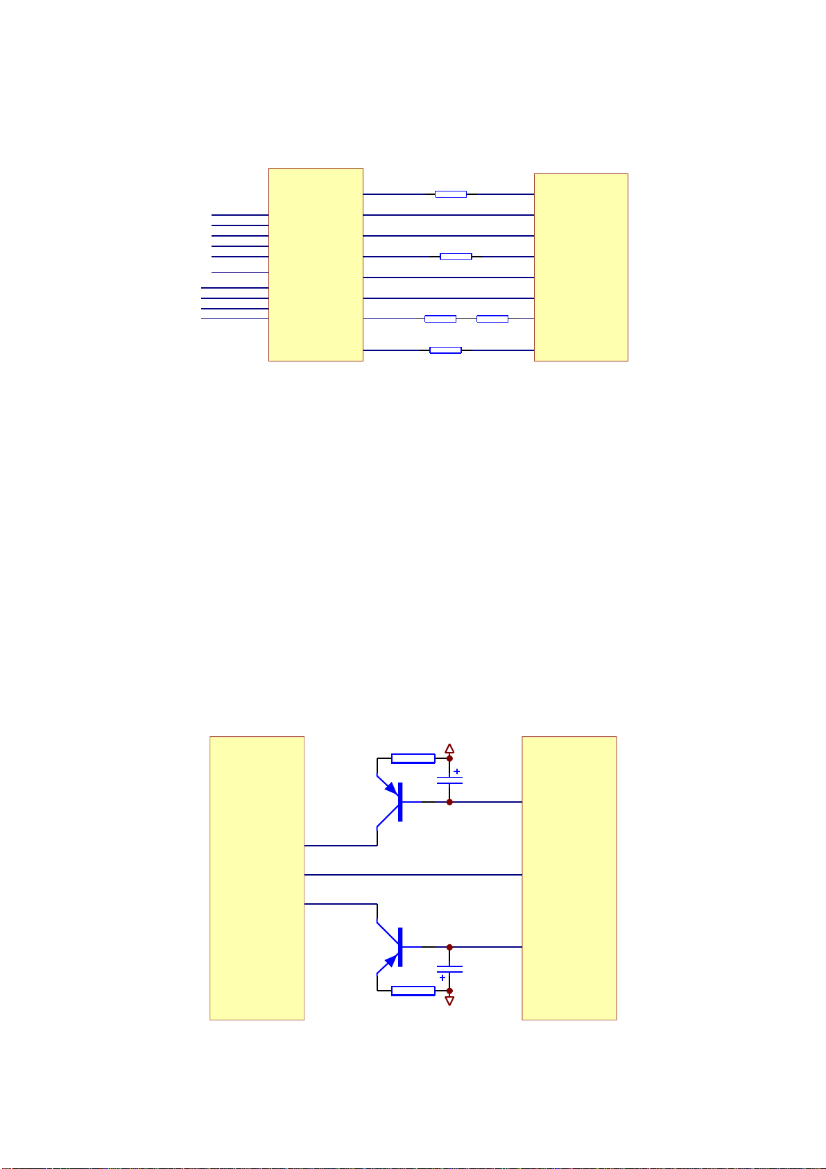
3.2.11Mutecircuit
1.Mutecircuitisshownasinthefigure3.2.11.1:
VCC
Q211
1015
VMUTE
R273
100K
89V33
E
TC220
100uF/16V
-9V
2.Workingprincipleofquietingcircuit
Whentheplayerisworkingnormally,showninthefigure3.2.11.1,MT1389Eoutputsanalogaudio
signal,andalowlevelsignalto
VMUTEatthesametimetomakeQ211on,BelectrodeofQ211isabout
R278
1K
R274
G
1K
E
R276
10K
AGND
Figure3.2.11.1Mutecircuit
2SC1815-YS
R275
10K
K
C296
105(DNS)
H
Q212
AGND
R277
10K
Q213
1015
I
D203
1N4148
MUTE-1
J
Q214
1015
D204
1N4148
M
AGND
R279
10K
TC221
100uF/16V
L
VCC
2.7V,collectorelectrodeofQ211isabout3.3V,soQ212isalsoon,voltageofBelectrodeisabout0.7V,
voltageofQ213Eelectrodeisneartozero,Q213cutsoff,MUTE1isnegativevoltage,whichisadded
-
tobaseelectrodeofmutetubeofaudiooutputendtomakemutetubecutoff,andaudiosignaloutputs
afterbeingamplifiedby4558.WhenpressingMUTEbuttononremotecontroller,MT1389hasnoaudio
-25-
Page 31

Signalthatoutputstooperationalamplifier,soaudiooutputendoftheplayerhasnoaudiosignaloutput,
butbecauseelectronicelementsincircuitwillproducesomenoisewhenworkingthattransmitstooutput
endoftheplayer,inordertofiltertherenoise,decodechipoutputsahighlevelsignaltoVMUTEtomake
Q211cutoff,soQ212cutsoff,+5VpoweristransmittedtobaseelectrodeofswitchpipeQ205-Q210
throughECelectrodeofQ213,mutecircuitisinmutestate.
Whenplayerisnotplayingdiscorstopsplaying,MT1389EoutputsahighlevelsignaltoVMUTEto
makeaudiocircuitentermutestate.
3.Power-offquietingworkingprinciple
Asshowninthefigure3.2.11.1,whentheplayerisworkingnormally,
D204ison,+5Vcharges
capacitorTC221throughD20,nowemittervoltageofQ214islessthanbaseelectrodevoltage,Q214
cutsoff.Whenpoweroff,+5Vdisappears,Q214baseelectrodechangesintolowlevel,itsemitter
electrodechangesintohighlevelbecauseofdischarge,nowQ214ison,Q214collectorelectrode
(AMUTE)outputshighleveltoaddtobaseelectrodeofswitchpipQ205-Q210,switchpipeissaturated,
noiseproducesinthecourseofpoweroffisbypassedtoground,andpower-ffquietingfunctionis
realized.
4.Keypointvoltage(unit:V)isshownasthefollowingtable:
Key point E F G H I J K L M
No mute 2.5 3.2 0.7 0.12 -0.15 -4.27 -4.27 4.9 4.9
Mute 3.2 -3.86 -3.87 1.4 0.7 1.3 -4 4.9 4.9
3.2.12Decodecircuitvoltageregulating
Decodecircuitvoltageregulatingisshownasinthefollowingfigure3.2.12:
MO-VCC
D301
1N4001
D302
1N4001
U301
AM5888S
1.8V
C281
104
Figure3.2.12Decodecircuitvoltageregulatingcircuitdiagram
100uF/16V
TC307
REGO2
Q306
SS8550
-26-
R324
5.6K
R332
TR_B2
10K
Q309
Ss8550
TR_B1
Ss8550
Q308
12K
R323
Q307
SS8550
R325
20K
REGO1
TR_B1
DV33
TC306
100uF/16V
Page 32

2.Workingprinciple:
DV33voltageregulatingprocess:VCCreducesvoltagethroughD301,andsupplypowerforrear
stagecircuitthroughE-CelectrodeofQ307.R325/R323isfeedbackendsamplingresistor.
Voltageregulatingprinciple:Dv33voltageincreasesREGO1voltageincreasesTR_B1
voltageincreasesQ307VCEvoltageincreasesDV33voltagedecreases.
――――――
――――――
Voltageregulatingprincipleof1.8VisthesamewiththatofDV33,onlyadiode(D302)isaddedto
performvoltagereduction.
3.Keypointvoltage(unit:V)isshownasfollows:
Celectrodeof#Q307:3.95,Belectrode:3.35,Celectrode:2.25
Celectrodeof#Q306:3.25,Belectrode:3.55,Celectrode:1.95
#REGO1REGO2is1.25V
3.2.13Powercircuit
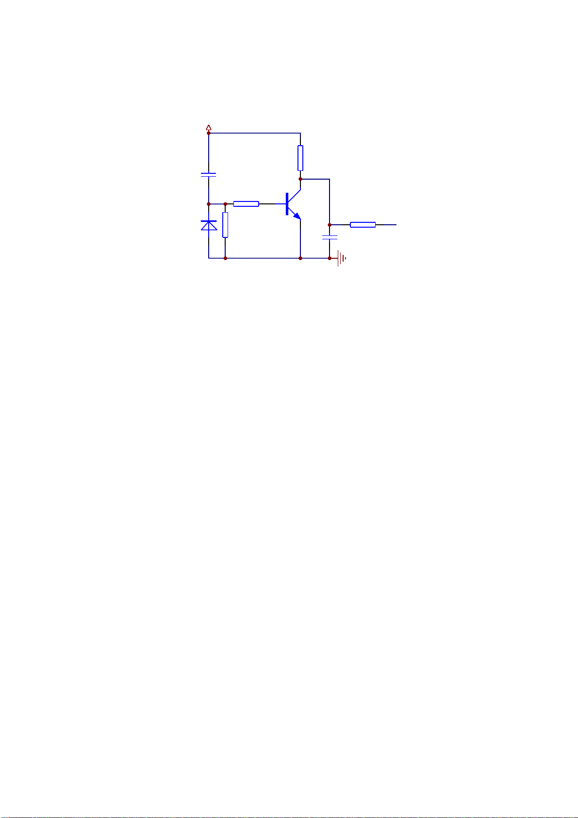
1.Powercircuitblockdiagramisshownasinthefollowingfigure3.2.13.1:
Rectification
Powergrid
filtering
Filtering
HOSTGND
SwitchIC
Absorptionloop
FSDH321
Feedback
winding
Rectification
Rectification
Rectification
Filtering
Filtering
Filtering
+5V
+9V
-9V
Photoelectric
coupling
Powersocket
TLV
431
Figure3.2.13.1Powercircuitblockdiagram
Sampling
circuit
2.Workingprinciple
(1)Powergridfilteringcircuit:variouselectromagneticradiationexistsinsurroundings,soitwill
produceinterferencetotheinputtedACpower,andthefunctionofpowergridfilteringcircuitistofilter
theseinterferencetomakethosethatenterbridgerectificationcircuitarepure220VACpower.
(2)Bridgerectificationandfilteringcircuit:thefunctionofthiscircuitistoconverseelectricsupply
intoDCpower,thevoltageafterbeingrectifiedandfilteredis1.414timesofinputpower,sotheDC
voltageatthetwoendsofTC501isaboutequalto300V。
-27-
Page 33

(3)Absorptionloop:forpowerisalwaysworkinginon/offstateandwillproduceveryhighpeak
voltage,inordertowellprotectswitchIC,apeakabsorptionloopisadded.
(4)Filteringcircuit:thefunctionistoproduceastableandslamm-waveDCvoltage.Infiltering
circuit,“"typefilterismostlyadopted.Thefeatureofcapacitorfilteringishighloadresistance,when
∏
currentissmall,filteringisobvious,butinductorfilteringissmallloadresistance,whencurrentislarge,
filteringisobvious.Tocomposecapacitorinto“"typefiltercanmakebetterfilteringeffect.
∏
(5)Feedbackloop:thetimelengthof“on”and“off”withinthesamecycleinsideswitchmodule
FSDH321
isdecidedbyfeedbackloop.Feedbackloopperformssamplingto+5Voutputstagevoltage,
whenoutputstagevoltageistoohigh,thesampledvoltageisonhighside,throughfeedbackloop,to
changethedutyratioofpin3signalofandreduceontime,andoutputvoltagebeginstoreduce.
FSDH321
Whenoutputvoltageistoolow,thesampledvoltageisonlowside,throughfeedbackloop,tomakeduty
radioofincrease,outputvoltageincreases,throughthefunctionoffeedbackloop,powerboard
FSDH321
ismadetooutputstablevoltage.TheusedLM431inthispowerisa2.5Vcomparator,samplingvoltage
iscomparewiththis2.5Vvoltage,whensamplingvoltageismorethan2.5V(meansthatoutputvoltage
isonhighside),LM431ison,lightemittingdiodeinphotoelectricdiodebeginstoemitlighttomakethe
otherendofphotoelectriccouplerbegintobeon,lightemittingdiodeisstronger,theondegreebigger,
theontimeofswitchmoduledecreases,outputvoltagebeginstodecrease.Whensampling
FSDH321
voltageislessthan2.5V(meansoutputstagevoltageisonlowside),Lm431iscutoff,ontimeof
FSDH321
increases,outputvoltageincreases.Thusthroughautocontrolfunctionoffeedbackloop,
powerboardismadetooutputstablevoltage.
3.2.14MICcircuit
1.MICcircuitblockdiagramisshownasinthefollowingfigure3.2.14.1:
VCC
-9V
+9V
DET
MIC
U603
amplifying
Figure3.2.14.1MICcircuitblockdiagram
U603
amplifying
TOMPEG
2.Workingprinciple:MICpart:aftermicrophoneisinsertedinMICleft,DETsignalschangefrom
highleveltolowlevel,Q601iscutofftomakemutecircuitofdecodepartoffatthesametime,nomatter
discreadingisavailable,audiosignalmayoutput.Ifthissignalappearstrouble,microphonewillhaveno
soundwhenplaybackstops.Signalsinputtedinmicrophone,afterbeingfiltered,outputtopin3ofU603
andsignalsafterbeingamplifiedoutputfrompin2ofU603,throughamplifyingthesecondtime,output
XS601
OK
frompin7ofU603todecodeboardforKaraokesignalprocessingandoverlapwithoutaudiosignalto
outputtorealizeKaraokefunction.
-28-
Page 34

Aftermicrophoneisunplugged,DETsignalchangesfromlowleveltohighlevel,Q601issaturated
on,MICsignalisinmutestatetoavoidaffectingrearstageaudiooutput.
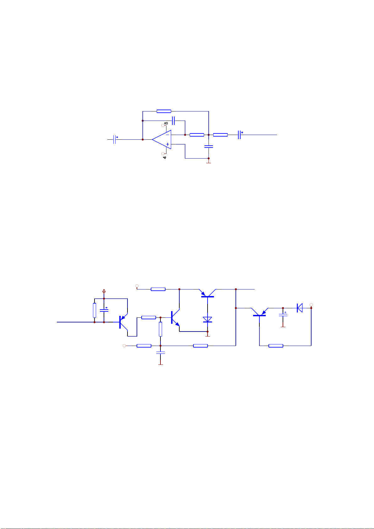
3.2.15Headphonecircuit
1.Headphonecircuitblockdiagramisshownasinthefollowingfigure3.2.15.1:
H-R
XS602
Figure3.2.15.1Headphonecircuitblockdiagram
H-L
U604TDA1308
Headphoneamplifying
R
JK601
Headphonesocket
L
2.Workingprinciple:H_L/H_Rsignalsofaudiooutputendtransmittoheadphoneamplifyingcircuit
ofMICboardthroughXS603,andheadphoneamplifyingcircuitismainlycomposedofU604(TDA1308).
Showninthefigure3.2.15.2,functionofmainpinsofTDA1308:pin1,7isoutputpin,pin6,2isinputpin.
Afterbeingamplified,audiosignalsoutputtoheadphonesocket(JK601)directly.
XS602
1
2
3
3P2.0
H_R
H_L
A5V
R615
1K
R617
56K
R627
3.3K
R628
3.3K
R616
1K
R618
56K
TC603
47uF/16V
C608
105
TC604
47uF/16V
R619
3.9K
TC607
47uF/16V
R620
3.9K
C609
101
R621
4.3K
R622
4.3K
C610
101
A5V
TC605
100uF/16V
U604
TDA1308
TC606
100uF/16V
R623
10K
R624
10K
C611
104(NC)
R625
22R(NC)
R626
22R(NC)
C612
104(NC)
C613
104(NC)
C614
104(NC)
Jk601
PHONEJACK
Figure3.2.15.2Headphonecircuitdiagram
3.1.16AVoutputboardcircuit
1.AVoutputboardismainlycomposedofAVoutputterminal,
circuitandfilteringcircuit.outputboardoutputsdifferentsignalsconnectedwiththecorresponding
AV
externalequipment,andamplifiesaudiosignaltransmissionMICboardthroughsocket
throughheadphone.AVoutputboardcircuitblockdiagramisshownasinthefollowingfigure3.1.16.1:
-29-
SCARToutputterminal,modeswitch
XS702tooutput
Page 35

PDAT2
PDAT1
+10V
R#
L#
VIEDO#
Y1
Pb
Pr
SPDIF
XS701
Figure3.1.16.1AVoutputboardcircuitblockdiagram
Mode
switch
RGB_CVBS
AV_TV
SCART
Component
videooutput
terminal
Optical,
coaxial
terminal
2.IntroductiontoSCARTterminal
(1)Workingprinciple:SCARTterminalintegratesvideoandaudioalltogetheranditmaytransmit
videoandaudiosignalsatthesametime.Theoperationisconvenient,21pinsinallandliesinthe
centralpartontherearsideoftheplayer.
(2)SCARTterminalpinfunctionisshownasthefollowingtable:
Pin Name
1 A(B)OUT I Audio right channel input 12 NC Network communication data line 2
2 A(B)IN O Audio right channel output 13 RETURN Pr signal ground
3 A(A)OUT I Audio left channel input 14 RETURN Blanking signal ground
4 A-COM Audio signal ground 15 RED I/O I/O Pr signalI/O port
5 RETURN Pb signal ground 16 BLK I/O I/O
6 A(A)IN O Audio left channel output 17 RETURN Blanking signal ground
7 BLUE I/O I/O Pb signalI/O port 18 TRTURN Composite video signal ground
8 FUNCSW I Function selection jack 19 V-OUT I Composite video signal input
9 RETURN Y1 signal ground 20 V-IN O Composite video signal output
10 CONT I/O
11 GREEN I/O I/O Y1 signal I/O port
Signal
direction
Function description Pin Name
Network communication data
line 2
21 GND Common
Signal
direction
Function description
Blanking signal I/O port ★
(3)SCARTterminalfunctionselectionisshownasthefollowingtable:
PDATO PDAT1 PDAT2 Pin 8 of SCART terminal Function
0 × 0 10V AV4:3
0 × 1 7.5V AV16:9
-30-
Page 36

1 × 0 0.90V TV
1 × 1 0.85V TV
× 0 × × CVBS MODE
× 1 × × RGB MODE
Note:PDAT0andPDAT2areusedtocontrolinputvoltageofpin8ofSCARTterminal;PDAT1is
usedtocontrolvoltagechangeofpin16ofSCARTterminalandthevoltageonpin16controlsSCART
terminaltoselectRGBmodeorCVBSmode.
3.2.17Controlpanelcircuit
1.Controlpanelcircuitblockdiagramisshowninthefollowingfigure3.2.17.1:
LEDscreen
9DV983-0
Subsidiary
board
Grid1~Grid7
XS402
LED
KEY2
S1
LEDAT
Figure3.2.17.1Controlpanelcircuitblockdiagram
PT6961
LEDCK
LEDST
XS401
Seg1~Seg10
S1S2
KEY1~3
XS403
IR
A983E-0
Buttonboard
Remotecontrol
receiver
2.Workingprinciple
Buttonfunctionrealization:whenusersareoperatingmachines,buttonmatrixcircuitwillproducea
buttonfunctioncodeandtransmittothemainCPUinsidedecodechip,andCPUperformsthe
correspondingswitchtothefunctionmoduleinsidesystem,andasignalwillproduceatthesametimeto
controlOSDandpaneldisplayparttomakethecorrespondingdisplay.
Paneldisplaydrive:whentheserialdatasignalsentbydecodechipistransmittingtopanelIC
(PT6961),ICperformsLEDdriveaccordingtotheinformationsentbydecodeanddisplaysthe
correspondingcontent(controlledbysoftware).
Indicatorlightcontrolcircuit:itiscontrolledbyFSOchipofdecodechiptoindicatorlight.
Definitionandfunctionofmainjacksofpanel:XS402isconnectedtosubsidiarypanel,withthe
functionoftransmittingbuttoncontrolsignalandindicatorlightcontrolvoltage;XS401isconnectedto
-31-
Page 37

Decodeboardandjackcommunicatedwithdecodesystem,inwhichIRisremotecontrolsignaloutput
pin,+5Vispanelpowersupply;LEDATisdatatransmissionpin(dualdirection)andiscontrolledby
LEDST,LEDCKistheworkingclocksignalinputdisplayedonpanel;FSOisthecontrolpinbyfirmware
topanellight;XS403isconnectedtobuttonboardwiththefunctionoftransmittingbuttoncontrolsignal.
-32-
Page 38

SectionThreeServicingCases
3.3.1Servicingcases
【】Example1Symptom:notreadDVDdisc
Description:focus,feed,mainaxisandtraceoflaserheadareallnormalbutdonotemitlight.
Analysisandtroubleshooting:poweroff,usemultimetertotesttriodeQ301anditisnotdamaged,
communicationofLD02and1389Eisnormal,poweronandchecktheworkingconditionofQ301and
findthatemitterelectrodeofQ301hasno3.3Vpower,check3.3Vpoweroftheplayeranditisnormal.
Showninthefigure3.3.1.1,3.3VisaddedtotheemitterelectrodeofQ301throughR301,sowedoubt
thatitiscausedbyfaultofR301,useresistancelevel(2K)totestandfindthatresistanceofresistoris
infinite.Afterchangingit,EelectrodepowerofQ301isnormal,DVDlaseremissionisnormaland
troubleisremoved.
LDO-AV33
R301
4.7R
TC302
【】
Example2Symptom:nosound
47uF/16V
Q301
2SB1132-S
Figure3.3.1.1APCcircuitdiagram
LDO2
Description:pictureoutputisnormal
Analysisandtroubleshooting:testsoundoutput,pin1,7ofcircuitoperationalam[lifierandthereis
nosignaloutput,testpowersupplyvoltageofoperationalamplifieranditis9Vwhichisonlowsidewith
onlytwoandalittle,afterremovingload,test9Vvoltageoutputofpowerboardanditisnormal,sowe
confirmthattroubleliesindecodeboard,onlyU209ofdecodeboardhas+9Vpowersupply,testthe
resistancetogroundofpin8ofU209anditis86,whichshouldbeinfiniteinnormalconditions,sowe
Ω
doubtthatU209hastrouble,changeitandtroubleisremoved.
-33-
Page 39

【】
Example3Symptom:powernoton
Description:nopicture,nosoundandnoscreendisplay
Analysisandtroubleshooting:showninthefigure3.3.1.2,afterpoweron,usevoltagelevel(20V)of
multimetertotestthepowersupplyfrompowerboardtodecodeboard(9,+5,3.3V)anditisnormal,
±
checkresetcircuitQ211workinganditisnormal,checkclockandthereisno27MHZoscillation
frequency,soitisdoubtedthatthefaultofcrystaloscillatorX201causedthetrouble,afterchangingit,
discreadingandoutputarenormalandtroubleisremoved.
R215 100K
【】
Example4Symptom:powernoton
XI
C275
33pF
Figure3.3.1.2Clockcircuitdiagram
X201
27MHz
XO
C276
33pF
Description:nopicture,nosoundandnoscreendisplay
Analysisandtroubleshooting:checkpowerboardandfindthatvoltageofeachchannelhasno
output,checkandfindthat220Vvoltageinputisnormal,testbridgerectificationcircuitandthereisno
voltageoutput,usemultimetertotestprotectortubeandithasopencircuit,changeprotectortubeand
troubleisnotremoved,testanodeofTc501andthereisstillnovoltageoutput,protectortubeisburnt
outagain,check4diodeofbridgerectificationcircuitandtheyareallnormal,TC501hasno
abnormalitiesofliquidleakageandstrickenthrough,testU501(switchIC)andpin1,8areshort-
circuitedtoground,soitisjudgedthatIChasbeenstrickenthrough,changeICandtroubleisremoved.
【】Example5Symptom:picturemosaicwhenreadingdisc
Description:poweronandreaddisc,afterdisplayingDVDformat,machinedownandpicturehas
mosaic,poweronagain,picturestillhasmosaicbutnotreaddisc.Putthemachineasidefor20minutes
andtroubledisappears.
Analysisandtroubleshooting:firstlytestvoltageofeachspot+5V,+3Vandcorevoltage1.86Vand
theyareallnormal,sowedoubtthatitisaffectedbytemperature.UseelectrichairdriertoheateachIC
ofdecodeboardandfindthatwhentemperatureofdecodeIC1389Eincreases20-degree,machine
downandpicturehasmosaic,change1389Echipandtroubleisremoved.
【】
Example6Symptom:nosound
Description:discreadingisnormalandthereissoundoutput
Analysisandtroubleshooting:useremotecontrollertorestoretodefaultsettingsfirstly,then
connectwithaudioterminalandcheckwhetherthereissoundoutput;checkpin1,7ofoperational
amplifierU209Ic4558andthereisnosoundoutput,testpin4,8of4558andthereisno+9Vvoltage,
-34-
Page 40

CheckandfindthatXS203has+9Vvoltageinput,testandfindthatoneendofL211has9Vvoltageand
theotherendhasnovoltageoutput,changeL210andtroubledisappears.
Example7Symptom:powernoton
【】
Description:noscreendisplayandnooutput
Analysisandtroubleshooting:check+5Vvoltageoutputofpowerboardanditisnormal;check
voltageofpin4ofXS203anditisalso+5V,whichisnormal;afterpowerofforaperiod,usehandto
touch1389andfindthat1389doesnotwork(feelthetemperaturehere.If1389hasbegantowork,the
temperaturewillbehigh),sofirstlyconsiderthepowersupplyof1389;showninthefigure3.3.1.3,test
anodeofTc307andthereisno+1.8Vvoltage(outputvoltageofQ307,Q308emitterelectrodesupplies
+3.3Vpowerfor1389),checkTC307,C281,R324,R323,Q306,Q309andtheyareallnormal,testbase
electrodevoltageofQ306anditiszero,thissignalisAM5888output,testvoltageofpin8,19,21of
AM5888andtheyareall5V,whichisnormal,sowejudgethatAM5888hastrouble;changeitand
troubleisremoved.
MO-VCC
D301
D302
1N4001
1N4001
TR_B1
DV33
TC306
100uF/16V
1.8V
C281
104
TR_B2
100uF/16V
TC307
REGO2
TR_B2
Q306
SS8550
R324
5.6K
10K
R332
Figure3.3.1.3circuitdiagram
Q309
Ss8550
TR_B1
Q308
Ss8550
12K
R323
Q307
SS8550
R325
20K
REGO1
【】Example8Symptom:powernoton
Description:poweron,testandfindthatthereisno+5V,3.3Vvoltageoutput.
Analysisandtroubleshooting:1.Insertpowercord,usemultimetertotestwhether220VACinputis
normal,andtheresultisnormal;
2.CheckwhethereachvoltageinputofXS203ondecodeboardisnormal,andfindthat+5Vhasno
inputbutothersarenormal;
3.PulloutflatcableofdecodeboardXS203,testeachinputvoltageagainandthereisstillno+5V
voltage;
4.Checkwhethertwoendsof+5VonpowersupplyflatcablefrompowerboardCN502todecode
board,andresultisnormal;
-35-
Page 41

5.TestvoltageoftwoendsofTC506,+5Vhasnooutput;afterpoweroff,use200ohmlevelof
multimetertotesttwoendsofTC506andfindthatresistanceisclosetozero,sowedoubtthatcapacitor
TC506haselectricityleakage;takedownTC506,testanodeweldingpointofTC506andfindthat+5V
outputisnormal,butthereisstillno3.3Voutput;
6.TesttwoendsofdiodeD507onpowerboardandfindthatoneendis5Vvoltageandtheother
endhasnovoltageoutput.AfterchangingD507,3.3Voutputisnormal,andmachineworksnormally.
【】Example9Symptom:headphonehasnosound
Description:audio,videooutputisnormal
Analysisandtroubleshooting:showninthefigure3.3.1.4,useoscillographtocheckpin1,3of
XS602onMICboardandthereiswaveformoutput;usemultimetertotestvoltageofpin3,5ofU604
(TDA1308)onMICboardanditis5Vwithoutabnormality;testvoltageofpin8anditisalso5V,power
supplyisnormal;useoscillographtotestpin2,6ofU604andthereiswaveforminput;checkpin1,7
andthereisnooutput,sowedoubtU603hastrouble;changeitandtroubleisremoved.
C609
101
XS602
1
2
3
3P2.0
H_R
A5V
H_L
R615
1K
R617
56K
R627
3.3K
R628
3.3K
R616
1K
R618
56K
TC603
47uF/16V
TC604
47uF/16V
R619
3.9K
C608
TC607
47uF/16V
105
R620
3.9K
Figure3.3.1.4Headphonecircuitdiagram
R621
4.3K
R622
4.3K
C610
101
A5V
TC605
100uF/16V
U604
TDA1308
TC606
100uF/16V
R623
10K
R624
10K
C611
104(NC)
R625
22R(NC)
R626
22R(NC)
C612
104(NC)
C613
104(NC)
C614
104(NC)
【】Example10Symptom:notreadDVD
Description:laserhead,focus,feed,mainaxisandtraceareallnormal,butnolightemission.
JK602
PHONEJACK
Analysisandtroubleshooting:checkemitterelectrodevoltageofQ301anditis3.3V,whichis
normal,testtheinductorL312betweencollectorelectrodeandpin23ofXs301andfindthatinductor
hasopencircuit;afterchanginginductor,troubleisremoved.
Example11Symptom:lessscreendisplay
【】
Description:whenreadingdisc,displayscreendoesnotemitlightforaperiod.
Analysisandtroubleshooting:beatmachineandtest,screenlessdisplayalwaysexists;usediode
levelofmultimeter,redpenconnectedwithanypinofscreenandblackpentestedpinofscreentube,
-36-
Page 42

testeachscreenpinonebyoneandchecklightemissionsegmentofscreenandasegmentof
screendoesnotemitlight,sowemayjudgethatscreenisdamaged;afterchangingscreen,troubleis
removed.
Example12Symptom:noMIC
【】
Description:soundoutputandpicturearenormalwhenreadingdisc
Analysisandtroubleshooting:poweron,useremotecontrollertoswitchonMIC,insertmicrophone
andspeak,showninthefigure3.3.1.5,useoscillographtopin5(OK)ofMICboardXS601andfindthat
thereisnosignaloutput;checkvoltageofpin4,8ofU603(+9V,-9V)anditisnormal;useoscillograph
totestpin3ofU603(4558)andthereissignalinput;testpin7ofU601andthereisnosignaloutput;
afterchangingU603,troubleisremoved.
R60410K
TC601
10uF/16V
R603
1K
C603 101
-9VA
2
3
R605
5.1K
+9VA
U603A
4558
C604
105
R606
5.1K
1
4
3MIC602
VCC
2
1
R610
5.1K
CK3-6.35-24
DET
【】
Example13Symptom:notreaddisc
L601
FB
L602
FBSMT
R611
12K
Figure3.3.1.5MICcircuitdiagram
C601
105
R601
10K
C607
103
R602
560R
C602
103
Description:notreadanydisc,laserhead,lightemission,feed,mainaxisandtraceareallnormal,
butthereisnofocusacts.
Analysisandtroubleshooting:usemultimetertotestpin13,14ofU301(5888)andvoltageis
normal(about1.4V),testpin1,2ofXS301andvoltageisnormal,checknerveflatcableandthecontact
isgood,sowejudgethatlaserheadfocuscoilisburntout;afterchangingloader,troubleisremoved.
【】
Example14Symptom:PLAYbuttonhasnofunction
Description:afterreadingdisc,pressPAUSEbuttonandthereisthisfunction;pressPLAYbutton
andthereisnothisfunction.
Analysisandtroubleshooting:takethemachineapart,useminimumresistanceofmultimetertotouch
thepenonthetwopinsnotadjacentoflighttouchswitch,pressdowntheswitchandfindthatthetwo
-37-
Page 43

pinshave10ohmresistance(oohmresistanceinnormalconditions),sowejudgethatlighttouchhas
trouble;afterchanginglighttouchswitch,troubleisremoved.
Example15Symptom:doornotopen
【】
Description:lightemission,mainaxisandfeedareallnormal,pressOPENbuttonandthereisno
acts.
Analysisandtroubleshooting:usemultimetertotestpin3of5PflatcableXS306fromframeto
decodeboardandvoltageoutputis+0.76Vwhichshouldbe+3.3V,testresistorR340betweenpin3and
1389anditis330ohm,whichisnormal,sowedoubtthat1389hastrouble,change1389andtroubleis
removed.
-38-
Page 44

3.3.2Troubleshootingflowchart
1.Troubleshootingprocessfor“Poweron(insert“powerplug”andturnon“powerswitch”)isshown
inthefollowingfigure3.3.2.1:
Poweron
Whether
power-onpicture
maybedisplayed
Y
N
Whether
3.3V,1.8Vpoweris
normal
Y
Check
whether27Mclockis
normal
Y
Whether
resetisnormal
Y
Check
whetherSDRAM
andFLASHpower
supplyis
normal
Y
Whether
firmwareisnormal
N
N
N
N
N
Whether
voltageregulating
circuitofDv331.8V
isnormal
Checkclockcircuit
Checkresetcircuit
Powersupplyloopand
filteringcircuit
Upgradeagain
N
Checkvoltageregulatingcircuit
Whether
discreadingisnormal
Y
A
Check
whetherclock
ofSDRAMis
normal
Check
whetherSDRAM
works
ChangeMT1389
N
Servocircuittroubleshooting
Y
Check
N
Y
N
Y
whetherFLSAH
andMT1389hasrosin
joint
Y
Weldagain
Check
whetherSDRAM
MT1389hasrosin
joint
Y
Weldagain
N
N
Change
Change
-39-
Page 45

A
Whether
soundisnormal
Y
Whether
screendisplayisnormal
N
N
whetherMT1389
hasaudiosignal
Checkaudiooutputcircuit
Whether
MT1389hassignalto
Checkpanelcircuit
Check
output
Y
panel
Y
N
CheckMT1389andpowersupply
N
Whether
firmwareiscorrect
Change1389
Figure3.3.2.1Troubleshootingflowchartfor“Poweron”
N
Upgradeagain
Y
-40-
Page 46

2.Troubleshootingprocessfor“Notreaddisc”isshowninthefollowingfigure3.3.2.2:
Notreaddisc
Whether
laserheadresets
Y
Whether
thereisfocusacts
Y
N
N N
Whether
pin26ofAM5888S
hasfeedsignal
input
Y
Check
whethervoltage
ofpin17/18ofAM5888S
isnormal
Y
CheckAM5888S
Whether
pin1ofAM5888S
hasfocussignal
input
Y
Check
whethervoltage
ofpin13,14ofAM5888S
isnormal
Y
N
CheckMT1389andfiltering
capacitor
N
Checkelectricmachine
CheckMT1389andfiltering
capacitor
N
CheckAM5888S
Whether
mainaxiselectric
machinerotates
Y
Whether
laserheademitslight
Y
B1
Checkthelinefrompin1,
2ofXS301tocoil
N
N
pin4ofAM5888Shas
whethervoltage
ofpin11,12ofAM5888S
Checkelectricmachine
whetherAPC
circuitsuppliesvoltage
forlaserhead
Changeloader
Whether
signalinput
Y
Check
isnormal
Y
Check
Y
N
CheckMT1389andfiltering
capacitor
N
N
CheckAM5888S
Check
whetherLDO_DV33is
normal
B2
N
Checkpowersupplycircuit
Y
-41-
Page 47

B2
B1
Whether
rotationspeedofdisc
isnormal
Y
Changeloader
N
threeisRsignalF Changeloader
thereisABCDEFsignal
Whether
Y
Whether
Y
Check
whetherLD01isnormal
Check
Q301,Q302andsocket
XS301
Change24Pflatcable
N
N
CheckXS301andflatcable
N
Y
N
Y
CheckMT1389
Change
CheckMT1389andtheperipheral
Figure3.3.2.2Troubleshootingflowchartfor“Notreaddisc”
-42-
Page 48

3.Troubleshootingprocessfor“Videohasnooutput”isshowninthefollowingfigure3.3.2.3:
Videohasnooutput
Check
whetheroutput
modeswitches
correctly
Y
Check
whether27Mclock
isnormal
Y
Whether
acertainvideosignal
hasnooutput
Y
Whether
componentvideohas
output
Y
Whether
compositevideohas
signaloutput
N
N
N
N
N
Resumesetupmode
Checkclockcircuit
Check
whetherpower
supplyofvideooutputof
MT1389is
normal
ChangeMT1389
Checkcomponentvideooutput
circuitwiththemethodthesame
withthatofcompositevideo
Whether
pin164of
MT1389hassignal
output
N
Checkpowersupplyloop
N
ChangeMT1389
Y
Check
whetherpin11
ofXS206hassignal
output
Y
CheckAVboardvideo
transmissionline
N
Checkvidefilteringcircuit
Figure3.3.2.3Troubleshootingflowchartfor“Videohasnooutput”
-43-
Page 49

4.Troubleshootingprocessfor“Nosoundoutput”isshowninthefollowingfigure3.3.2.4:
Nosoundoutput
Whether
+9V-9Vpowersupply
isnormal
Y
Whether
decodechiphasaudio
signaloutput
Y
Whether
partofchannelhas
nooutput
Y
Check
whethermachinesetup
isnormal
Y
Checkaccordingtotheprocess
of“Acertainchannelhasnosound”
N
N
N
N
Checkpowersupplyloop
Checkdecodechip
Checkwhethermute
Y
Cancelmute
Setagainorresume
N
Checkmutecircuit
Figure3.3.2.4Troubleshootingflowchartfor“Nosoundoutput”
-44-
Page 50

5.Troubleshootingprocessfor“Leftchannelhasnosound”isshowninthefollowingfigure3.3.2.5:
Leftchannelhasnosound
Check
whetherpin186
ofMT1389hassound
output
Y
Check
whetherpin2
ofU209hasaudiosignal
input
Y
Check
whetherpin1
ofU209hassignal
output
Y
Check
whetherpin13
ofXS206hassignal
output
Y
N
N
N
N
MT1389hastrouble
Checkthelinebetween
MT1389andU209
U209hastrouble
TestQ206
Whether
filteringcapacitor
haselectric
leakage
Y
Removeonebyone
N
Checklineandterminal
Figure3.3.2.5Troubleshootingflowchartfor“Leftchannelhasnosound”
-45-
Page 51

6.Troubleshootingprocessfor“MIChasnosoundoutput”isshowninthefigure3.3.2.6:
MIChasnosoundoutput
Check
whetherpin3
ofU603hassignal
input
Y
Check
whetherpin1
ofU603hassignal
output
Y
Check
whetherpin6
ofU601hassignal
input
Y
Check
whetherpin7
ofXS601hassignal
output
Y
N
N
N
N
CheckMICsocket
CheckU603andpower
supplyloop
Checktheelementbetween
pin1andpin6ofU603
Checkpin7ofU603andthe
linebetweenitandXS601
Whether
DETpinislowlevel
Y
Check
whetherQ601is
normal
Y
Check
whethertheline
todecodechipis
normal
Y
ChangeMT1389
N
N
N
ChangeMICsocket
ChangeQ601
Removeonebyone
Figure3.3.2.6Troubleshootingflowchartfor“MIChasnosoundoutput”
-46-
Page 52

7.Troubleshootingprocessfor"Headphonehasnosoundoutput"isshowninthefollowingfigure
3.3.2.7:
Headphonehasno
soundoutput
Check
whetherXS603has
signalinput
Y
Check
whetherpin6,2
ofTDA1308hassignal
input
Y
Check
whetherpin1,7
ofTDDA1308hassignal
Changeheadphonesocket
output
Y
Check
whetherheadphone
sockethassignal
input
Y
N
Checkaudioprocessing
circuit
N
Checktheelementandline
betweenX603andU603
N
CheckU603andpower
supplyloop
N
CheckthelinefromU603
outputpintoheadphone
socket
Figure3.3.2.7Troubleshootingflowchartfor“Headphonehasnosoundoutput”
-47-
Page 53

8.Troubleshootingprocessfor"No+5Vvoltage(powerboard5317SI-1)"isshowninthefollowing
figure3.3.2.8:
No+5Vvoltage
Whether
cathodeof
D510haspower
output
Y
Whether
pin4ofCN501
haspower
output
Y
OK
N
CheckD510andtransformer
N
Check+5Vfilteringcircuit
Figure3.3.2.8Troubleshootingprocessfor“No+5Vvoltage”
-48-
Page 54

9.Troubleshootingprocessfor"Voltageoutputisunstable(powerboard5317SI-1)"isshowninthe
followingfigure3.3.2.9:
Voltageoutputisunstable
Check
whetherLM431pinhas
voltage
Y
Check
whetherLM431is
normal
Y
Check
whetherphotoelectric
coupleris
normal
Y
ChangeU501,C506
N
CheckLM431andsampling
circuitR508R509C515R506
N
N
ChangeLM431
Changephotoelectriccoupler
Figure3.3.2.9Troubleshootingflowchartfor“Voltageoutputisunstable”
-49-
Page 55

10.Troubleshootingprocessfor“No+9Vvoltage(powerboard5317SI-1)”isshowninthefollowing
figure3.3.2.10:
No+9Vvoltage
Whether
D508cathodehas
poweroutput
Y
Whether
pin1ofCN501has
poweroutput
Y
OK
N
CheckD508andtransformer
N
Check+9Vfilteringcapacitor
Figure3.3.2.10Troubleshootingflowchartfor“No+9Vvoltage”
-50-
Page 56

11.Troubleshootingprocessfor“No-9Vvoltage(powerboard5317SI-1)”isshowninthefollowing
figure3.3.2.11:
No-9Vvoltage
Whether
cathodeofD511has
poweroutput
Y
Whether
pin2ofCN501has
poweroutput
Y
OK
N
CheckD511andtransformer
N
Check-9Vfilteringcapacitor
Figure3.3.2.11Troubleshootingprocessfor“No-9Vvoltage”
-51-
Page 57

12.Troubleshootingprocessfor“Novoltageoutput(powerboard5317SI-1)”isshowninthe
followingfigure3.3.2.12:
Novoltageoutput
Whether
twoendsofTC501
have300V
voltage
Y
Whether
voltageofeach
pinofU501is
normal
Y
CheckU501peripheral
andtransformer
Figure3.3.2.12Troubleshootingflowchartfor“Novoltageoutput”
N
N
twoendsofpower
gridfilterhaveAC
Checkrectificationtube
D501D504~
ChangeU501
Whether
input
Y
N
Checkpowercord
-52-
Page 58

SectionFour Waveformdiagram
Thissectioncollectssignalwaveformdiagramofaudio,videoandeachunitcircuitwiththepurpose
tohelpservicingpersonneltojudgewheretroubleliesinaccuratelyandquicklytoimproveservicing
skills.Forthedifferenceofoscillograph'stype,modelandtuner,acertaindifferencemayexist,sothe
servicingpersonnelareexpectedtopaymoreattentiontocheckindailyoperation.
XS3011.RFOsignalwaveformdiagramofpin8of
2.Asignalwaveformdiagramofpin9ofXs301(BCDEF、、、、)
-53-
Page 59

3.DMOsignal(whenthereismainaxisrotation)waveformdiagramofpin37ofU201(MT1389)
4.FMOsignal(whenthereisfeed)waveformdiagramofpin38ofU201(MT1389)
5.TROsignal(whenthereistrace)waveformdiagramofpin41ofU201(MT1389)
-54-
Page 60

6.FOOsignal(whenthereisfocus)waveformdiagramofpin42ofU201(MT1389)
7.Waveformdiagramofpin29(whennodiscin)ofU214(FLASH)
8.Waveformdiagramofpin38ofU211(SDRAM)
-55-
Page 61

9.Videosignalwaveformdiagram
10.Waveformdiagramofaudiosignalswithoutbeingfilteredandamplified(testpoint:audiosignal
amplifyinginputendTc241)
11.1KHZsignalwaveformdiagram.Itissuggestedtousetestdisc,ifnot,thetestedwaveformwill
changeatanytimetoaffectjudgment.
-56-
Page 62

12.LEF#:waveformdiagramforsubwooferchannelanalogsigna(DV521)l
13.SPDIF:waveformdiagramforoptical/coaxialdigitalaudiosignal
14. 27Mclocksignalwaveformdiagram
-57-
Page 63

15. Resetsignalwaveformdiagram
URST#
Dv33
-58-
Page 64

Section Five Function Introduction to IC
3.5.1 function introduction to MT1389E
1. DESCRIPTION
MT1389E is a cost-effective DVD system-on-chip (SOC) which incorporates advanced features like
MPEG-4 video decoder, high quality TV encoder and state-of-art de-interlace processing.
Based on MediaTek’s world-leading DVD player SOC architecture, the MT1389E is the 3rd generation of
the DVD player SOC. It integrates the MediaTek 2nd generation front-end analog RF amplifier and the
Servo/MPEG AV decoder.
To enrich the feature of DVD player, the MT1389 equips a simplified MPEG-4 advanced simple profile
(ASP) video decoder to fully support the DivX1 Home Theater profile. It makes the MT1389-based DVD
player be capable of playback MPEG-4 content which become more and more popular.
The progressive scan of the MT1389E utilized advanced motion-adaptive de-interlace algorithm to
achieve the best movie/video playback. It also supports a 3:2 pull down algorithm to give the best film effect.
The 108MHz/12-bit video DAC provides users a whole new viewing experience.
2. Key Features
RF/Servo/MPEG Integration
Embedded 6ch Audio DAC
Embedded 2ch Audio ADC for Karaoke
High Performance Audio Processor
High Performance Progressive Video Processor
Support Nero-Digital
High Quality 108MHz/12-bit, 4 CH TV Encoder
3. General Feature lists
(1)Integration DVD player single chip
High performance analog RF amplifier
Servo controller and data channel processing
MPEG-1/MPEG-2/JPEG video
Dolby AC-3/DTS Decoder
Unified memory architecture
-59 -
Page 65

Versatile video scaling & quality enhancement
OSD & Sub-picture
Built-in clock generator
Built-in high quality TV encoder
Built-in progressive video processor
Audio effect post-processor
Built-in 5.1-ch Audio DAC
Built-in 2-ch Audio ADC for Karaoke
(2)High Performance Analog RF Amplifier
Programmable fc
Dual automatic laser power control
Defect and blank detection
RF level signal generator
(3)Speed Performance on Servo/Channel Decoding
DVD-ROM up to 4XS
CD-ROM up to 24XS
(4)Channel Data Processor
Digital data slicer for small jitter capability
Built-in high performance data PLL for channel data demodulation
EFM/EFM+ data demodulation
Enhanced channel data frame sync protection & DVD-ROM sector sync protection
(5)Servo Control and Spindle Motor Control
Programmable frequency error gain and phase error gain of spindle PLL to control spindle motor on CLV
and CAV mode
Built-in ADCs and DACs for digital servo control
Provide 2 general PWM
Tray control can be PWM output or digital output
(6)Embedded Micro controller
Built-in 8032 micro controller
Built-in internal 373 and 8-bit programmable lower address port
1024-bytes on-chip RAM
Up to 2M bytes FLASH-programming interface
-60-
Page 66

Supports 5/3.3-Volt. FLASH interface
Supports power-down mode
Supports additional serial port
(7)DVD-ROM/CD-ROM Decoding Logic
High-speed ECC logic capable of correcting one error per each P-codeword or Q-codeword
Automatic sector Mode and Form detection
Automatic sector Header verification
Decoder Error Notification Interrupt that signals various decoder errors
Provide error correction acceleration
(8)Buffer Memory Controller
Supports 16Mb/32Mb/64Mb SDRAM
Supports 16-bit SDRAM data bus
Provides the self-refresh mode SDRAM
Block-based sector addressing
(9)Video Decode
Decodes MPEG1 video and MPEG2 main level, main profile video (720/480 and 720x576)
Decodes MPEG-4 Advanced Simple Profile
Support DivX 3.11/4.x/5.x Home Theater Profile
Support Nero-Digital
Smooth digest view function with I, P and B picture decoding
Baseline, extended-sequential and progressive JPEG image decoding
Support CD-G titles
(10)Video/OSD/SPU/HLI Processor
Arbitrary ratio vertical/horizontal scaling of video, from 0.25X to 256X
65535/256/16/4/2-color bitmap format OSD,
256/16 color RLC format OSD
Automatic scrolling of OSD image
(11)Audio Effect Processing
Dolby Digital (AC-3)/EX decoding
DTS/DTS-ES decoding
MPEG-1 layer 1/layer 2 audio decoding
MPEG-2 layer1/layer2 2-channel audio
-61 -
Page 67

High Definition Compatible Digital (HDCD)
Windows Media Audio (WMA)
Dolby ProLogic II
Concurrent multi-channel and downmix out
IEC 60958/61937 output
PCM / bit stream / mute mode
Custom IEC latency up to 2 frames
Pink noise and white noise generator
Karaoke functions
Microphone echo
Microphone tone control
Vocal mute/vocal assistant
Key shift up to +/- 8 keys
Chorus/Flanger/Harmony/Reverb
Channel equalizer
3D surround processing include virtual surround and speaker separation
(12)TV Encoder
Four 108MHz/12bit DACs
Support NTSC, PAL-BDGHINM, PAL-60
Support 525p, 625p progressive TV format
Automatically turn off unconnected channels
Support PC monitor (VGA)
Support Macrovision 7.1 L1, Macrovision 525P and 625P
CGMS-A/WSS
Closed Caption
(13)Progressive Scan Video
Automatic detect film or video source
3:2 pull down source detection
Advanced Motion adaptive de-interlace
Minimum external memory requirement
(14)Outline
216-pin LQFP package
3.3/1.8-Volt. Dual operating voltages
- 62-
Page 68

4. PIN DESCRIPTION
PIN
191
192
212
213
214
215
216
1 AGND Ground Analog ground
2 DVDA Analog input AC couple input path A
3 DVDB Analog input AC couple input path B
4 DVDC Analog input AC couple input path C
5 DVDD Analog input AC couple input path D
Main Alt Type Description
RF interface (26)
RFGND18 Ground Analog ground
RFVDD Power Analog power 1.8V
OSP Analog output RF Offset cancellation capacitor connecting
OSN Analog output RF Offset cancellation capacitor connecting
RFGC Analog output RF AGC loop capacitor connecting for DVD-ROM
Current reference input. It generates reference current for RF
IREF Analog input
path. Connect an external 15K resistor to this pin and AVSS
AVDD3 Power Analog power 3.3V
6 DVDRFIP Analog input AC coupled DVD RF signal input RFIP
7 DVDRFIN Analog input AC coupled DVD RF signal input RFIN
8 MA Analog input DC coupled main beam RF signal input A
9 MB Analog input DC coupled main beam RF signal input B
10 MC Analog input DC coupled main beam RF signal input C
11 MD Analog input DC coupled main beam RF signal input D
12 SA Analog input DC coupled sub-beam RF signal output A
13 SB Analog input DC coupled sub-beam RF signal output B
14 SC Analog input DC coupled sub-beam RF signal output C
15 SD Analog input DC coupled sub-beam RF signal output D
16 CDFON Analog input CD focusing error negative input
17 CDFOP Analog input CD focusing error positive input
18 TNI Analog input 3 beam satellite PD signal negative input
19 TPI Analog input 3 beam satellite PD signal positive input
ALPC (4)
20 MIDI1 Analog input Laser power monitor input
21 MIDI2 Analog input Laser power monitor input
22 LDO2 Analog output Laser driver output
-63 -
Page 69

23 LDO1 Analog output Laser driver output
Reference voltage (3)
28 V2REFO Analog output Reference voltage 2.8V
29 V20 Analog output Reference voltage 2.0V
30 VREFO Analog output Reference voltage 1.4V
Analog monitor output (7)
24 SVDD3 Power Analog power 3.3V
25 CSO RFOP Analog output
1) Central servo
2) Positive main beam summing output
1) RFRP low pass, or
26 RFLVL RFON Analog output
2) Negative main beam summing output
27 SGND Ground Analog ground
31 FEO Analog output Focus error monitor output
32 TEO Analog output Tracking error monitor output
33 TEZISLV Analog output TE slicing Level
Analog Servo Interface (8)
204
205
206
207
208
209
ADCVDD3 Power Analog 3.3V power for ADC
ADCVSS Ground Analog ground for ADC
RFVDD3 Power Analog power
RFRPDC Analog output RF ripple detect output
RFRPAC Analog input RF ripple detect input (through AC-coupling)
HRFZC Analog input High frequency RF fipple zero crossing
210
211
195
196
197
198
199
200
201
202
203
CRTPLP Analog output Defect level filter capacitor connecting
RFGND Ground Analog power
RF Data PLL Interface (9)
JITFO Analog output Output terminal of RF jitter meter
JITFN Analog Input Input terminal of RF jitter meter
PLLVSS Ground Ground pin for data PLL and related analog circuitry
IDACEXLP Analog output Data PLL DAC Low-pass filter
PLLVDD3 Power Power pin for data PLL and related analog circuitry
LPFON Analog Output Negative output of loop filter amplifier
LPFIP Analog input Positive input terminal of loop filter amplifier
LPFIN Analog input Negative input terminal of loop filter amplifier
LPFOP Analog output Positive output of loop filter amplifier
- 64 -
Page 70

Motor and Actuator Driver Interface (10)
34 OP_OUT Analog output Op amp output
35 OP_INN Analog input Op amp negative input
36 OP_INP Analog input Op amp positive input
37 DMO Analog output Disk motor control output. PWM output
38 FMO Analog output Feed motor control. PWM output
39 TROPENPWM
Analog output Tray PWM output/Tray open output
40 PWMOUT1 ADIN0 Analog output
41 TRO Analog output
42 FOO Analog output
LVTTL3.3 Input,
FG
ADIN1
Schmitt input, pull up,
43
(Digital pin)
GPIO
with analog input path
for ADIN1
General Power/Ground (11)
48
84
DVDD18 Power 1.8V power pin for internal digital circuitry
132
146
3) 1st General PWM output
4) AD input 0
Tracking servo output. PDM output of tracking servo
compensator
Focus servo output. PDM output of focus servo
compensator
1) Monitor hall sensor input
2) AD input 1
3) GPIO
74
DVSS Ground 1.8V ground pin for internal digital circuitry
120
60
87
DVDD3 Power 3.3V power pin for internal digital circuitry
108
137
149
DVSS Ground 3.3V ground pin for internal digital circuitry
Micro Controller and Flash Interface (48)
54 HIGHA0 InOut 4~16mA,SRPU Microcontroller address 8
66 HIGHA1 InOut 4~16mA,SRPU Microcontroller address 9
65 HIGHA2 InOut 4~16mA,SRPU Microcontroller address 10
64 HIGHA3 InOut 4~16mA,SRPU Microcontroller address 11
63 HIGHA4 InOut 4~16mA,SRPU Microcontroller address 12
-65 -
Page 71

62 HIGHA5 InOut 4~16mA,SRPU Microcontroller address 13
61 HIGHA6 InOut 4~16mA,SRPU Microcontroller address 14
59 HIGHA7 InOut 4~16mA,SRPU Microcontroller address 15
81 AD7 InOut 4~16mA,SRPU Microcontroller address/data 7
78 AD6 InOut 4~16mA,SRPU Microcontroller address/data 6
77 AD5 InOut 4~16mA,SRPU Microcontroller address/data 5
76 AD4 InOut 4~16mA,SRPU Microcontroller address/data 4
75 AD3 InOut 4~16mA,SRPU Microcontroller address/data 3
73 AD2 InOut 4~16mA,SRPU Microcontroller address/data 2
72 AD1 InOut 4~16mA, Microcontroller address/data 1
71 AD0 InOut 4~16mA,SRPU Microcontroller address/data 0
83 IOA 0 InOut 4~16mA,SRPU Microcontroller address
69 IOA 1 InOut 4~16mA,SRPU Microcontroller address 1/ IO
47 IOA 2 InOut 4~16mA,SRPU Microcontroller address 2/ IO
49 IOA 3 InOut 4~16mA,SRPU Microcontroller address 3/ IO
50 IOA 4 InOut 4~16mA,SRPU Microcontroller address 4/ IO
51 IOA 5 InOut 4~16mA,SRPU Microcontroller address 5/ IO
52 IOA 6 InOut 4~16mA,SRPU Microcontroller address 6/ IO
53 IOA 7 InOut 4~16mA,SRPU Microcontroller address 7/ IO
58 A16 InOut 4~16mA,SRPU Flash address 16
82 A17 InOut 4~16mA,SRPU Flash address 17
InOut 4~16mA,
55 A18
Flash address 18 /IO
SRPD,SMT
InOut 4~16mA,
56 A19
Flash address 19 /IO
SRPD,SMT
YUV0
InOut 4~16mA,
5) Flash address 20 /IO 6) While External Flash size <=
67 A20
YUV7
SRPD,SMT
InOut 4~16mA,
1MB: I) Alternate digital video YUV output 0
7) Flash address 21 /IO 8) While External Flash size <= 2MB:
79 A21
GPIO
SRPD,SMT
I) Digital video YUV output 7 II) GPIO
InOut 4~16mA,
80 ALE
Microcontroller address latch enable
SRPD,SMT
70 IOOE#
Flash output enable, active low / IO
SRPD,SMT
57 IOER# InOut 4~16mA, Flash write enable, active low / IO
InOut 4~16mA,
-66 -
Page 72

SRPD,SMT
68 IOCS#
85 UWR#
86 URD#
88 UP1_2
89 UP1_3
91 UP1_4
92 UP1_5
93 UP1_6 SCL
InOut 4~16mA,
SRPD,SMT
InOut 4~16mA,
SRPD,SMT
InOut 4mA,
SRPD,SMT
InOut 4~16mA,
SRPD,SMT
InOut 4mA,
SRPD,SMT
InOut 4mA,
SRPD,SMT
InOut 4mA,
SRPD,SMT
InOut 4mA,
SRPD,SMT
Flash chip select, active low / IO
Microcontroller write strobe, active low
Microcontroller read strobe, active low
Microcontroller port 1-2
Microcontroller port 1-3
Microcontroller port 1-4
Microcontroller port 1-5
9) Microcontroller port 1-6
10) I2C clock pin
94 UP1_7 SDA
95 UP3_0 RXD
96 UP3_1 TXD
RXD
97 UP3_4
SCL
RXD
98 UP3_5
SDA
102
103
IR Input SMT IR control signal input
INT0#
InOut 4mA,
SRPD,SMT
InOut 4mA,
SRPD,SMT
InOut 4mA,
SRPD,SMT
InOut 4mA,
SRPD,SMT
InOut 4~16mA,
SRPD,SMT
InOut 4~16mA,
SRPD,SMT
11) Microcontroller port 1-7
12) I2C data pin
13) Microcontroller port 3-0
14) 8032 RS232 RxD
15) Microcontroller port 3-1
16) 8032 RS232 TxD
17) Microcontroller port 3-4
18) Hardwired RD232 RxD
19) I2C clock pin
20) Microcontroller port 3-5
21) Hardwired RD232 TxD
22) I2C data pin
Microcontroller external interrupt 0, active low
1) Audio left/right channel clock
153
ALRCK
YUV1
GPO
InOut 4mA,
2) Trap value in power-on reset:
PD,SMT
I) 1: use external 373
-67 -
Page 73

II) 0: use internal 373
153
151
152
154
ALRCK
ABCK
ACLK
ASDATA0
YUV1
GPO
YUV0
GPIO
YUV0
GPIO
YUV2
GPO
InOut 4mA,
PD,SMT
InOut 4mA,
SMT
InOut 4mA,
SMT
InOut 4mA,
PD,SMT
3) While internal audio DAC used:
I) Digital video YUV output 1
II) GPO
4) Audio bit clock
5) While internal audio DAC used:
I) Digital video YUV output 0
II) GPIO
6) Audio DAC master clock
7) While internal audio DAC used:
I) Alternate digital video YUV output 0
II) GPIO
8) Audio serial data 0 (Front-Left/Front-Right)
9) Trap value in power-on reset:
I) 1: manufactory test mode
II) 0: normal operation
10) While internal audio DAC used:
155
156
157
ASDATA1
ASDATA2
ASDATA3
YUV4
GPO
YUV5
GPO
YUV6
GPIO
InOut 4mA,
PD,SMT
InOut 4mA,
PD,SMT
InOut 4mA,
PD,SMT
I) Digital video YUV output 2 II) GPO
11) Audio serial data 1 (Left-Surround/Right-Surround)
12) Trap value in power-on reset:
I) 1: manufactory test mode
II) 0: normal operation
13) While only 2 channels output:
I) Digital video YUV output 4 II) GPO
14) Audio serial data 2 (Center/LFE)
15) Trap value in power-on reset:
I) 1: manufactory test mode
II) 0: normal operation
16) While only 2 channels output:
I) Digital video YUV output 5 II) GPO
17) Audio serial data 3 (Center-back/
Center-left-back/Center-right-back, in 6.1 or 7.1 mode)
18) While only 2 channels output:
I) Digital video YUV output 6
II) GPIO
158
MC_DATA INT2# InOut 2mA, 19) Microphone serial input
-68 -
Page 74

YUV0 20) While not support Microphone:
I) Microcontroller external interrupt 2
II) Digital video YUV output 0
III) GPIO
Output
159
172
173
174
175
176
177
178
179
180
181
182
183
SPDIF
4~16mA,
S/PDIF output
SR: ON/OFF
AADVSS Ground Ground pin for 2ch audio ADC circuitry
AKIN2 Analog Audio ADC input 2
ADVCM Analog 2ch audio ADC reference voltage
AKIN1 Analog Audio ADC input 1
AADVDD Power 3.3V power pin for 2ch audio ADC circuitry
APLLVDD3 Power 3.3V Power pin for audio clock circuitry
APLLCAP Analog InOut APLL external capacitance connection
APLLVSS Ground Ground pin for audio clock circuitry
ADACVSS2 Ground Ground pin for audio DAC circuitry
ADACVSS1 Ground Ground pin for audio DAC circuitry
21) Audio DAC sub-woofer channel output
ARF GPIO Output
22) While internal audio DAC not used: GPIO
23) Audio DAC right Surround channel output
ARS GPIO Output
24) While internal audio DAC not used: GPIO
184
185
186
187
188
189
25) Audio DAC right channel output
26) While internal audio DAC not used:
AR GPIO Output
a. SDATA1
b. GPIO
AVCM Analog Audio DAC reference voltage
27) Audio DAC left channel output 28) While internal audio
AL Output
DAC not used: a. SDATA2 b. GPIO
29) Audio DAC left Surround channel output
30) While internal audio DAC not used:
ALS Output
c. SDATA0
d. GPIO
31) Audio DAC center channel output
ALF Output
32) While internal audio DAC not used: GPIO
ADACVDD1 Power 3.3V power pin for audio DAC circuitry
- 69 -
Page 75

190
ADACVDD2 Power 3.3V power pin for audio DAC circuitry
Video Interface (12)
160
161
162
163
164
165
166
167
168
169
170
171
DACVDDC Power 3.3V power pin for video DAC circuitry
VREF Analog Bandgap reference voltage
FS Analog Full scale adjustment
DACVSSC Ground Ground pin for video DAC circuitry
InOut 4mA,
CVBS
Analog composite output
SR
DACVDDB Power 3.3V power pin for video DAC circuitry
DACVSSB Ground Ground pin for video DAC circuitry
DACVDDA Power 3.3V power pin for video DAC circuitry
InOut 4mA,
Green, Y, SY, or CVBS
Y/G
SR
DACVSSA Ground Ground pin for video DAC circuitry
InOut 4mA,
B/CB/PB
Blue, CB/PB, or SC
SR
InOut 4mA,
R/CR/PR
Red, CR/PR, CVBS, or SY
SR
101
PRST#
PD,SMT
InOut
100
193
194
ICE InOut PD,SMT Microcontroller ICE mode enable
XTALO Output 27MHz crystal output
XTALI Input 27MHz crystal input
VSYN
InOut 4mA,
44 GPIO0
YUV1
SR,SMT
HSYN
InOut 4mA,
45 GPIO1
INT4#
SR,SMT
YUV2
46 GPIO2 SPMCLK InOut 2mA
MISC (12)
Power on reset input, active low
33) General purpose IO 0
34) Vertical sync for video input
35) Digital video YUV output 1
36) General purpose IO 1
37) Horizontal sync for video input
38) Microcontroller external interrupt 4
39) Digital video YUV output 2
40) General purpose IO 2
41) Audio S/PDIF SPMCLK input
147
GPIO3
InOut 2mA
SPDATA
INT1#
42) General purpose IO 3
43) Microcontroller external interrupt 1
-70-
Page 76

44) Audio S/PDIF SPDATA input
148
GPIO4 SPLRCK InOut 2mA
INT3#
150
GPIO5
SPBCK
90 GPIO6 YUVCLK
99 GPIO7 YUV3
145
144
143
142
RA4 InOut DRAM address 4
RA5 InOut DRAM address 5
RA6 InOut DRAM address 6
RA7 InOut DRAM address 7
45) General purpose IO 4
46) Audio S/PDIF SPLRCK input
47) General purpose IO 5
InOut 2mA
48) Microcontroller external interrupt 3
49) Audio S/PDIF SPBCK input
InOut 4mA,
50) General purpose IO 6
SR,SMT
51) Digital video clock output
InOut 4mA,
SR,SMT
52) General purpose IO 7
53) Digital video YUV output 3
Dram Interface (38) (Sorted by position)
141
140
139
138
136
135
134
133
131
130
129
128
127
126
125
RA8 InOu DRAM address 8
RA9 InOut DRAM address 9
RA11 InOut Pull-Down DRAM address bit 11
CKE Output DRAM clock enable
RCLK InOut Dram clock
RA3 InOut DRAM address 3
RA2 InOut DRAM address 2
RA1 InOut DRAM address 1
RA0 InOut DRAM address 0
RA10 InOut DRAM address 10
BA1 InOut DRAM bank address 1
BA0 InOut DRAM bank address 0
RCS# Output DRAM chip select, active low
RAS# Output DRAM row address strobe, active low
CAS# Output DRAM column address strobe, active low
124
123
122
RWE# Output DRAM Write enable, active low
DQM1 InOut Data mask 1
RD8 InOut DRAM data 8
- 71 -
Page 77

121
RD9 InOut DRAM data 9
119
118
117
116
115
114
113
112
111
110
109
107
106
105
104
RD10 InOut DRAM data 10
RD11 InOut DRAM data 11
RD12 InOut DRAM data 12
RD13 InOut DRAM data 13
RD14 InOut DRAM data 14
RD15 InOut DRAM data 15
RD0 InOut DRAM data 0
RD1 InOut DRAM data 1
RD2 InOut DRAM data 2
RD3 InOut DRAM data 3
RD4 InOut DRAM data 4
RD5 InOut DRAM data 5
RD6 InOut DRAM data 6
RD7 InOut DRAM data 7
DQM0 InOut Data mask 0
3.5.2 function introduction to 4558
1. Description
The RC4558 and RM4558 devices are dual general-purpose operational amplifiers with each half
electrically similar to the A741 except that offset null capability is not provided.?
The high common-mode input voltage range and the absence of latch-up make these amplifiers ideal for
voltage-follower applications. The devices are short-circuit protected and the internal frequency compensation
ensures stability without external components.
The RC4558 is characterized for operation from 0 C to 70 C, and the RM4558 is characterized for ? ?
operation over the full military temperature range of –55 C to 125 C.
2. FEATURES
◆ Continuous-Short-Circuit Protection
◆ Wide Common-Mode and Differential
◆ Voltage Ranges
◆ No Frequency Compensation Required
◆ Low Power Consumption
◆ No Latch-Up
-72 -
Page 78

◆ Unity-Gain Bandwidth . . . 3 MHz Typ
◆ Gain and Phase Match Between Amplifiers
◆ Low Noise . . . 8 nV?Hz Typ at 1 kHz
◆ Designed To Be Interchangeable With
◆ Raytheon RC4558 and RM4558 Devices
3. PIN CONFIGURATION
PIN No Symbol I/O
1 1OUT O
2 1IN– I
3 1IN+ I
PIN No. Symbol I/O
PIN No. Symbol I/O
4 VCC– I
5 2IN+ I
6 2IN– I
7 2OUT O
8 VCC+ I
3.5.3 function introduction to AT24C02
1. Description
Description
Output 1
Inverting Input Pin 1
Non-Inverting Input Pin 1
Description
Description
Negative Power Supply
Non-Inverting Input Pin 2
Inverting Input Pin 2
Output 2
Positive Power Supply
The AT24C02 provides 2048 bits of serial electrically erasable and programmable read-only memory
(EEPROM) organized as 256 words of 8 bits each. The device is optimized for use in many industrial and
commercial applications where low-power and low-voltage operation are essential. The AT24C02 is available
in space-saving 8-lead PDIP,
8-lead MAP, 8 lead TSSOP and 8-ball dBGA2 packages and is accessed via a 2-wire serial interface. In
addition, the entire family is available in 2.7V (2.7V to 5.5V) and 1.8V (1.8V to 5.5V) versions.
2. Features
◆ Low-voltage and Standard-voltage Operation
– 2.7 (VCC = 2.7V to 5.5V)
– 1.8 (VCC = 1.8V to 5.5V)
◆ Internally Organized, 256 x 8 (2K),
◆ 2-wire Serial Interface
◆ Schmitt Trigger, Filtered Inputs for Noise Suppression
-73 -
Page 79

◆ Bi-directional Data Transfer Protocol
◆ 100 kHz (1.8V) and 400 kHz (2.5V, 2.7V, 5V) Compatibility
◆ Write Protect Pin for Hardware Data Protection
◆ 8-byte Page (1K, 2K), Write Modes
◆ Partial Page Writes are Allowed
◆ Self-timed Write Cycle (5 ms max)
◆ High-reliability
◆ – Endurance: 1 Million Write Cycles
◆ – Data Retention: 100 Years
◆ Automotive Grade, Extended Temperature and Lead-Free Devices Available
◆ 8-lead PDIP, 8-lead JEDEC SOIC, 8-lead MAP, 5-lead SOT23,
◆ 8-lead TSSOP and 8-ball dBGA2™ Packages
3. PIN DESCRIPTION
PIN No. Symbol I/O Description
1 A0 I To Ground
2 A1 I To Ground
3 A2 I To Ground
4 VSS I To Ground
5 SDA I/O Serial Data input
6 SCL I/O Serial SCL input
7 TEST I/O Test port
8 VDD I Positive Power Supply
3.5.4 function introduction to TDA1308
1. DESCRIPTION
The TDA1308; TDA1308A is an integrated class AB stereo headphone driver contained in an SO8, DIP8
or a TSSOP8 plastic package. The device is fabricated in a 1 mmCMOS process and has been primarily
developed for portable digital audio applications.
The difference between the TDA1308 and the TDA1308A is that the TDA1308A can be used at low
supply voltages.
2. FEATURES
◆ Wide temperature range
?◆ No switch ON/OFF clicks
-74 -
Page 80

?◆ Excellent power supply ripple rejection
?◆ Low power consumption
◆ Short-circuit resistant
?◆ High performance
◆ – high signal-to-noise ratio
◆ – high slew rate
◆ – low distortion
?◆ Large output voltage swing.
3. PIN DESCRIPTION
PIN Symbol I/O Description
1 OUTA O output A
2 INA(neg) I inverting input A
3 INA(pos) I non-inverting input A
4 VSS I negative supply
PIN Symbol I/O Description
5 INB(pos) I non-inverting input B
6 INB(neg) I inverting input B
7 OUTB O output B
8 VDD I positive supply
3.5.5 function introduction to VIPer22ADIP
1. DESCRIPTION
The VIPer22A combines a dedicated current mode PWM controller with a high voltage Power MOSFET
on the same silicon chip. Typical applications cover off line power supplies for battery charger adapters,
standby power supplies for TV or monitors, auxiliary supplies for motor control, etc. The internal control circuit
offers the following benefits:
– Large input voltage range on the VDD pin accommodates changes in auxiliary supply voltage. This
feature is well adapted to battery charger adapter configurations.
– Automatic burst mode in low load condition.
– Overvoltage protection in hiccup mode.
2. FEATURES
◆ FIXED 60 KHZ SWITCHING FREQUENCY
◆ 9V TO 38V WIDE RANGE VDD VOLTAGE
-75 -
Page 81

◆ CURRENT MODE CONTROL
◆ AUXILIARY UNDERVOLTAGE LOCKOUT WITH HYSTERESIS
◆ HIGH VOLTAGE START UP CURRENT SOURCE
◆ OVERTEMPERATURE, OVERCURRENT AND OVERVOLTAGE PROTECTION WITH
AUTORESTART
3. PIN DESCRIPTION
PIN Symbol I/O Description
1 SOURCE O Power MOSFET source and circuit ground reference.
2 SOURCE O Power MOSFET source and circuit ground reference.
3 FB I Feedback input.
4 VDD I Power supply of the control circuits.
5 DRAIN I Power MOSFET drain.
6 DRAIN I Power MOSFET drain.
7 DRAIN I Power MOSFET drain.
8 DRAIN I Power MOSFET drain.
3.5.6 function introduction to AM5888S
1. Description
The AM5888S is a five-channel BTL driver IC for driving the motors and actuators such as used in DVD
player and consists of two independent precision voltage regulators with adjustable range from 1.5V to 4 V. It
supports a variety of applications. Also, Pb free package is selectable (Please refer to Marking Identification).
2. Fetures
1) Two channels are voltage-type BTL drivers for actuators of tracking and focus. Two channels are
voltage-type BTL driver for sled and spindle motors. It is also built-in one channel bi-direction DC motor driver
for tray.
2) Wide dynamic range [9.0V (typ.) when Vcc1= Vcc2= 12V, at RL= 20¦¸ load].
3) Separating power of Vcc1 and Vcc2 is to improve power efficiency by a low supply voltage for tracking,
focus, and spindle.
4) Level shift circuit built-in.
5) Thermal shut down circuit built-in.
6) Mute mode built-in.
7) Dual actuator drivers:
A general purpose input OP provides differential input for signal addition. The output structure is two
-76 -
Page 82

power OPAMPS in bridge configuration.
8) Sled motor driver:A general purpose input OP provides differential input for signal addition. The output
structure is one power OPAMP in bridge configuration.
9) Spindle driver:Single input linear BTL driver. The output structure are two power OPAMPS in bridge
configuration.
10) Tray in-out driver:The DC motor driver supports forward/reverse control for tray motor.
11) 2 Built-in regulator controllers: Adjustable range 1.5V ~ 4V
3. PIN DESCRIPTION
PIN Symbol I/O Description
1 VINFC I Input for focus drive
2 TRB_1 O Connect to external transistor base
3 REGO2 O Regulator voltage output, connect to external transistor collector
4 VINSL I Input for the sled driver
5 REGO1 O Regulator voltage output, connect to external transistor collector
6 FWD I Tray driver forward input
7 REV I Tray driver reverse input
8 VCC1 I Vcc for pre-drive block and power block of sled and tray
9 VOTR- O Tray driver output (-)
10 VOTR+ O Tray driver output (+)
11 VOSL+ O Sled driver output (+)
12 VOSL- O Sled driver output (-)
13 VOFC- O Focus driver output (-)
14 VOFC+ O Focus driver output (+)
15 VOTK+ O Tracking driver output (+)
16 VOTK- O Tracking driver output (-)
17 VOLD+ O Spindle driver output (+)
18 VOLD- O Spindle driver output (-)
19 VCC2 I Vcc for power block of spindle, tracking and focus
20 NC No Connection
21 VCTL I Speed control input of tray driver
22 GND I Ground
23 VINLD I Input for spindle driver
24 NC No Connection
-77 -
Page 83

25 TRB_2 O Connect to external transistor base
26 VINTK I Input for tracking driver
27 BIAS I Input for reference voltage
28 MUTE I Input for mute control
3.5.7 function introduction to PT6961(4dv315)
1. DESCRIPTION
PT6961 is an LED Controller driven on a 1/7 to 1/8 duty factor. Eleven segment output lines, six grid
output lines, 1 segment/grid output lines, one display memory, control circuit, key scan circuit are all
incorporated into a single chip to build a highly reliable peripheral device for a single chip microcomputer.
Serial data is fed to PT6961 via a four-line serial interface. Housed in a 32-pin SO Package, PT6961 pin
assignments and application circuit are optimized for easy PCB Layout and cost saving advantages.
2. FEATURES
◆ CMOS Technology
◆ Low Power Consumption
◆ Multiple Display Modes (12 segment, 6 Grid to 11 segment, 7 Grid)
◆ Key Scanning (10 x 3 Matrix)
◆ 8-Step Dimming Circuitry
◆ Serial Interface for Clock, Data Input, Data Output, Strobe Pins
◆ Available in 32-pin, SOP Package
3. PIN DESCRIPTION
PIN Symbol I/O Description
1 OSC I Oscillator Input P in
2 DOUT O Data output
3 DIN I Data input
4 CLK I Clock input
5 STB I Serial interface strobe
6 K1 I Key data input
7 K2 I Key data input
8 K3 I Key data input
9 VDD I Power supply
10 SG1/KS1 O Segment output
-78 -
Page 84

11 SG2/KS2 O Segment output
12 SG3/KS3 O Segment output
13 NC
14 SG4/KS4 O Segment output
15 SG5/KS5 O Segment output
16 SG6/KS6 O Segment output
17 SG7/KS7 O Segment output
18 SG8/KS8 O Segment output
19 SG9/KS9 O Segment output
20 SG10/KS10 O Segment output
21 SG11 O Segment output
22 SG12/GR7 O Segment output
23 GR6 O Grid output
24 GR5 O Grid output
25 VDD I Power input
26 GND I Ground
27 GR4 O Grid output
28 GR3 O Grid output
29 GND I Ground
30 GR2 O Grid output
31 GR1 O Grid output
32 GND I Ground
3.5.8 Function introduction to SDRAM
64M 16-bit memorizer SDRAM with the player and the working clock frequency is 166/143MHZ. The
function of 16SDRAM in DVD players is to memorizer the program of AML3298 taken out from FLASH and
information of image and sound taken out from disc to form buffer, add the stability of information output and
add anti-shaking effect of player. Pin function introduction is shown as the following table:
Pin Name
1 VDD 3.3V power supply 28 VSS Ground
2 DQ0 Data bus I/O 29 MA4 Address bus I
Function Signal flow Pin Name Function Signal flow
-79 -
Page 85

3 VDDQ
4 DQ1 Data bus I/O 31 MA6 Address bus I
5 DQ2 Data bus I/O 32 MA7 Address bus I
3.3V power supply I/O 30 MA5 Address bus I
6 VSSQ
7 DQ3 Data bus I/O 34 MA9 Address bus I
8 DQ4 Data bus I/O 35 MA11 Address bus I
9 VDDQ
10 DQ5 Data bus I/O 37 CKE Clock enable signal I
11 DQ6 Data bus I/O 38 CLK System clock input I
12 VSSQ
13 DQ7 Data bus I/O 40 NC Blank
14 VDD 3.3V power supply 41 VSS Ground
15 LDQM
16
WE Write control signal I 43 VDDQ
17 CAS Line address gating signal I 44 DQ9 Data bus I/O
Data input/output screen-shielded
Ground 33 MA8 Address bus I
3.3V power supply 36 NC Blank
Ground 39 UDQM
I 42 DQ8 Data bus I/O
signal
Data input/output
I
screen-shielded signal
3.3V power supply
18 RAS Row address gating signal I 45 DQ10 Data bus I/O
19
20 SD-BS0 Segmanr address 0 gating signal
21 SD-BS1 Segmanr address 1 gating signal
22 MA10
23 MA0 Address bus I 50 DQ13 Data bus I/O
24 MA1 Address bus I 51 DQ14 Data bus I/O
25 MA2 Address bus I 52 VSSQ Ground
26 MA3 Address bus I 53 DQ15 Data bus I/O
27 VDD 3.3V power supply 54 VSS Ground
CS Chip selection signal I 46 VSSQ Ground
I 47 DQ11 Data bus I/O
I 48 DQ12 Data bus I/O
Address bus I 49 VDDQ
3.3V power supply
3.5.9 Function introduction to FLASH
FLASH (U214) is a 16Mbit FLASH memorizer, and the damage of U214 may cause troubles, such as
power not on, no disc reading and power on picture mosaic. Pin function is shown as the following table:
-80-
Page 86

Pin Name Function Voltage (when no disc) Data direction
R
1-9、16-25、48
11 WE Write enable signal, low level is effective 3.23V I
12 RESET Reset, low level is effective 3.23V I
10、13、14
15 RY/BY Ready/system busy 3.23V O
26 CE Chip enable, low level effective 0V I
27、46
28 OE Output enable signal , low level is effective 0V I
29-3、6、38-44
37 VCC 5V power supply +5V
45 DQ15/A-1
47 BYTE
AO-A19 20 bit address bus I
NC Blank pin
VSS Ground
DQ0-DQ14
Take word extend mode as data line, and bit extend
Select 8-bit or 16-bit output mode. High level is 16-bit
output and low level is 8-bit output
15 bit data bus O
I/O
mode as address line
I
3.5.10 Function introduction to LM431A
U503 (LM431A) is a 2.5V comparator, shown as the figure 3.4.12.1. Compared the inputted voltage of R end
with 2.5V, when voltage of R end is more than 2.5V, KA end is on and photoelectric coupler starts to send out
photocurrent; when voltage of R end is less than 2.5V, KA end is cutoff and photoelectric coupler does not send
out photocurrent. CPU+3.3V in power board circuit must be kept in 3.3V, for the function of comparator. No
matter more than or less than 3.3V, through on and off status of comparator, it will control the on state of the
output end of photoelectric coupler LM431A to adjust the output space occupation ratio of switch module to
control the output voltage of transformer and masthead the power.
K
A
Figure 3.4.12.1 LM431A outside drawing
3.5.11 Function introduction to Pc817
U502 (2501) is a photoelectric coupler, shown as the figure 3.4.13.1. The right side is a light emitting diode,
which sends out light of different intensity according to the strength of voltage inputted from the right side,
generates photocurrent of different intensity on the left side according to light of different intensity, and outputs
- 81 -
Page 87

from position D. The higher of the voltage inputted from the right side, the stronger of the light emitted from
light emitting diode and the larger of the photocurrent produced from position D. The lower of the voltage
inputted from the right side of photoelectric coupler, the weaker of the light emitted from light emitting diode
and the weaker of the current outputted from position D.
Figure 3.4.13.1 2501 outside drawing
-82 -
Page 88

ChapterFour
DisassemblyandAssemblyProcess
DVDplayersmanufacturedinBBKarelargelyidenticalbutwithminordifferencesandaremainly
composedofloadercomponents,controlpanelcomponents,decodeandservoboardcomponents,
powerboardcomponents,poweramplifierboardcomponents,MICboardcomponentsandAVboard
components.Inordertospeedupthecompilationof“ServiceManual”,weshallnotgiverepeat
explanationtomodelwithminordifferencesinchapterfour“DisassemblyandAssemblyProcess”forthe
latercompiledservicemanuals.Fordisassemblyandassemblyprocessinthischapter,pleasereferto
chapter4of“DK1005SServiceManual”or“DK1020SService”.
Thepicturesofthismodelareshownasfollows:
-83-
Page 89

Chapter Cinque
PCB board & Circuit diagram
Section One PCB board
5.1.1 Surface layer of AV OUT Board
JK706
XS702
R709
L713
R708
R711
L714
7231-0
DVD 2006/1/17
V703
V702
R712
JP709
LEI
- 84 -
JP702
V701
JP721
JP722
JP712
JK705
JP724
JP723
JP720
XS701
PDAT2
JP718
PDAT1
SPDIF
VCC
JK702
JP704
JP728
PR
VGND
JP729
AGND
G702
R
+10V
JP727
JP719
JP726
JP725
PB
(PD)
VGND
VIEDOLPDAT0
Y1
VGND
Page 90

5.1.2 Bottom layer of AV OUT Board
C710
L708
R717
C722
R721
C717
L707
R702
R701
C720
L709
C711
R703
R714
R706
C727
R705
R715
ZD704
R704
R710
C716
C723
C724
C728
R713
R716
D701
D702
C725
C726
ZD701ZD702ZD703
R718
R719
- 85 -
Page 91

5.1.3 Bottom layer of KEY SCAN Board
LED401
DVD 2005/11/11
4983E-1
O
TC401
U402
V
G
TC402
- 86 -
Page 92

5.1.4 Surface layer of KEY SCAN Board
KEY3
KEY2
KEY1
XS403
S2#
S1#
VD401
L401
VD402
R402
R403
R404
D407
R407
D401D402D403
C401
D404
C408
Q401
R406
G13
S1#
R409
KEY2
LED01
C402
R410
R411
XS402
R401
U401
D411D410D409
D406C403
R408
R405
XS401
- 87 -
Page 93

5.1.5 Bottom layer of MIC Board
- 88 -
Page 94

5.1.6 Surface layer of MIC Board
- 89 -
Page 95

5.1.7 Bottom layer of MPEG&SERVO Board
- 90 -
Page 96

5.1.8 Surface layer of MPEG&SERVO Board
- 91 -
Page 97

5.2.1 MPEG&SERVO Board 1
Section Two circuit diagram
R2123
10K
C2117
102
R2124
10K
C2118
102
R2125
10K
C2119
102
R2126
10K
C2120
102
R271
36K(NC)
R272
36K(NC)
30K
R2111
C2111 100pF
1
7
1
+A9V
7
-A9V
+A9V
1
-A9V
+A9V
7
-A9V
+A9V
-A9V
R109 1
+A9V
-A9V
C2116 150pF
+A9V
-A9V
R2112
C2112 100pF
C2113 150pF
C2114 150pF
U210A
4 8
4580
R2115
C2115 150pF
U211B
4 8
4580
R2116
4 8
R2135
Q205
2SC1815-YS
Q206
2SC1815-YS
Q207
2SC1815-YS
Q208
2SC1815-YS
Q209
2SC1815-YS
2SC1815-YS
1K
R2136
1K
R2137
1K
R2138
1K
R2139
1K
R2140
1K
R2141
1K
R2142
1K
R2143
1K
R2144
1K
R2145
1K
R2146
1K
Rt
R2147
100K
AGND
R2148
100K
Lt
SR
R2149
100K
AGND
SL
LFE
Cc
R2150
100K
R2151
100K
R2152
100K Q210
- 92 -
MUTE-1
MUTE-1
MUTE-1
CH-R
CH-L
CH-SR
CH-SL
CH-SW
CH-C
TC246
10uF/16V
TC247
10uF/16V
TC248
10uF/1206
TC249
10uF/1206
TC250
10uF/1206
TC251
10uF/1206
4 8
4 8
R2113
4 8
R2114
U211A
4580
U209B
4580
30K
U209A
4580
U210B
4580
2
3
30K
6
5
30K
R2117
4.7K
6
5
AGND
R2118
4.7K
2
3
AGND
30K
R2119
4.7K
6
5
AGND
30K
R2120
4.7K
AGND
R2121
R2127
4.7K
10K
C2121
102
AGND
R2122
R2128
4.7K
AGND
10K
C2122
102
2
3
OKA
AGND
R
L
SR#
SL#
SW
CTR
C2129
102(DNS)
R205
0R
TC240
10uF/16V
TC241
10uF/16V
TC242
10uF/16V
TC243
10uF/16V
TC244
10uF/16V
TC245
10uF/16V
OK
89_AR
89_ARS
89_ALS
89_SW
89_CTR
89_AL
VMUTE
R273
100K
89V33AGND
+9V
AGND
-9V
AGND
DET
OK
GND
+9V
-9V
VCC
TC220
100uF/16V
C2130
104(DNS)
C2133
104(DNS)
MIC_DET
MIC_IN1
MIC_IN2
473
C297
-9V
C2131
104(DNS)
C2134
104(DNS)
VCC
Q211
1015
C298
C2132
TC222
100uF/16V(DNS)
104(DNS)
C2135
TC223
100uF/16V(DNS)
104(DNS)
330R
R265
R266
0R
R267 0R
102(DNS)
473
C299
XS205
1
2
3
C328
101
R276
10K
R274
1K
R278
1K
AGND
4
5
6
R275
10K
2.0mm
C296
105(DNS)
OK OKA#
Q213
1015
Q212
2SC1815-YS
AGND
R277
10K
D203
1N4148
C292
105
DET
OKA#
OKA#
89V33
AGND
MUTE-1
ZD203
3V/0.5W
ZD204
2.7V/0.5W
Q214
1015
R279
10K
AGND
D204
1N4148
TC221
100uF/16V
VCC
Page 98

VREF
SPDIF
ALRCK
ACLK
ABCK
GPIO5
DVSS
GPIO4
GPIO3
RA11
DVDD3
RCLK
RA10
RCS#
RAS#
CAS#
RWE#
DQM1
DVSS
RD10
RD11
RD12
RD13
RD14
RD15
RA4
RA5
RA6
RA7
RA8
RA9
CKE
RA3
RA2
RA1
RA0
BA1
BA0
RD8
RD9
RD0
RD1
RD2
RD3
RD4
C276
33pF
FS
DACVDD3 89V33
L206
FBSMT
TC212
10uF/16V
4.7K
R270
ASDAT2
R207 1K
ALRCK
R206 560R
FS
C216 104
VREF
R223
75R
89V33 V18
FS
VREF
DACVDD3
IEC958
AMDAT
ASDAT3
ASDAT2
ASDAT1
ASDAT0
ALRCK
ACLK
ABCK
TROUT
TRIN
LIMIT
-12V
162
161
160
159
158
157
156
155
154
153
152
151
150
149
148
147
146
145
144
143
142
141
140
139
138
137
136
135
134
133
132
131
130
129
128
127
126
125
124
123
122
121
120
119
118
117
116
115
114
113
112
111
110
109
C242
104
SPDIFIEC958
VMUTE
MA4
MA5
MA6
MA7
MA8
MA9
MA11
DCKE
DCLK
MA3
MA2
MA1
MA0
MA10
BA1
BA0
CS#
RAS#
CAS#
WE#
DQM1
DQ8
DQ9
DQ10
DQ11
DQ12
DQ13
DQ14
DQ15
DQ0
DQ1
DQ2
DQ3
DQ4
5.2.2 MPEG&SERVO Board 2
C243
104
AVCC
2SK3018-S
R329
10K
R340 330R
R377 330R
C311
103
Q305
3904-S
Q304
4.7uH
FBSMT
4.7uH
FBSMT
1R
LIMIT#
R309
10K
R311
10K
R310
100K
U301
15
VOTK+
16
VOTK-
17
VOLD+
18
VOLD-
19
VCC2
20
NC
21
PVCC
30
GND2
22
PREGND
23
VINLD
24
NC
25
TR_B2
26
VINTK
27
BIAS
MUTE28VINFC
AM5888S
DV33
SL+
SL-
SP+
SP-
R320
150K
R318
680K/1%
TROUT
TRIN
AVCC
R315
330
C301
104
MDI
E
V20
F
B
A
RFO
IOA
D
C
TKTK+
FC+
FC-
C307 222
R317
680K/1%
IOA
220uF/16V
VOFC+
VOFCVOSL+
VOSL-
VOTR+
VOTR-
VCC1
GND1
REV
FWD
REGO1
VINSL+
REGO2
TR_B1
TC301
LIMIT
C309
222
89V33
14
13
12
11
10
9
8
29
7
6
5
4
3
2
1
C308
101(DNS)
L316
FBSMT
R301
LDO-AV33
4.7R
Q301
2SB1132-S
Q302
2SB1132-S
R302
LDO-AV33
4.7R
FCSPSP+
LOAD+
LOADMO-VCC
GND
TRCLOSE
TROPEN
REGO1
REGO2
FOSO
R331
0R
OPOP+
V1P4
TC302
47uF/16V
TC303
47uF/16V
RFVDD3
C237
222
OPO
ADIN
C281
104
LDO-AV33
C318
104
LDO2
LDO1
C238
103
R314
10K
C319
104
C239
104
C316
104
TC307
100uF/16V
C236
C246
104(DNS)
C317
104
PLLVDD3
C229
104
AADVDD3
104
C247
104(DNS)
L203
FBSMT
MO-VCC
100uF/16V
DMSO
Q306
SS8550
R324
5.6K
L201
V18 RFV18
FBSMT
R303
10R
TC207
100uF/16V
L202
4.7uH
TC208
220uF/16V
C249
C248
104
104(DNS)
89V33
L204
330uH
L315
FBSMT
TC304
MO-VCC
D302
1N4001
10K
R332
C230
104
89V33
89V33
89V33
C250
104
C240
103
VCC
DMSO
FMSO
TRSO
FOSO
V1P4
C210
153
D301
1N4001
Q309
SS8550(DNS)
1.8V
TC209
220uF/16V
ADACVDD3
C207
104
C208
104
C209
104
C212
C211
331
104
SS8550(DNS)
Q308
12K
R323
TC210
220uF/16V
C2154
105
C2156
105
C2158
105
R201
R202
R203
R204
C213
331
TR_B1TR_B2
L219
FBSMT
C2155
105
C2157
105
C2159
105
R325
20K
REGO1REGO2
RFO
Q307
SS8550
V18
C231
104
C
B
A
D
C205 105(DNS)
C206
101
C214
104
10K
15K
27K
27K
TR_B1TR_B2
100uF/16V
C201 105
C202 105
C203 105
C204 105
C
B
A
D
SUBA
SUBB
SUBC
SUBD
E
F
MDI
LDO2
LDO1
RFOP
RFON
V2P8
V20
V1P4
FEO
TEO
TEZISLV
OPO
OPOP+
DMO
FMO
TROPEN
V1P4_IN
TRO
FOO
ADIN
VSYNC#
HSYNC#
STBY
A2
A3
A4
A5
A6
A7
A8
DV331.8V
TC306
C232
104
RFVDD3
V18
C233
104(DNS)
C260
104
R211
15K
C234
104(DNS)
RFVDD3
1
2
3
4
5
6
7
8
9
10
11
12
13
14
15
16
17
18
19
20
21
22
23
24
25
26
27
28
29
30
31
32
33
34
35
36
37
38
39
40
41
42
43
44
45
46
47
48
49
50
51
52
53
54
89V33
C226
104
104
C227
C228
216
215
AVDD3
AGND
DVDA
DVDB
DVDC
DVDD
DVDRFIP
DVDRFIN
MA
MB
MC
MD
SA
SB
SC
SD
CDFON
CDFOP
TNI
TPI
MDI1
MDI2
LDO2
LDO1
SVDD3
CSO/RFOP
RFLVL/RFON
SGND
V2REFO
V20
VREFO
FEO
TEO
TEZISLV
OP_OUT
OP_INN
OP_INP
DMO
FMO
TROPENPWM
PWMOUT1/ADIN0
TRO
FOO
FG/ADIN1
GPIO0/VSYNC#
GPIO1/HSYNC#
GPIO2
IOA2
DVDD18
IOA3
IOA4
IOA5
IOA6
IOA7
HIGHA0
IOA18
55
56
A18
A19
333
214
IREF
IOA19
57
PWR#
C225
213
OSN
RFGC
A16
IOWR#
58
A16
R210
100K
104
212
59
A15
OSP
211
RFGND
DVDD360HIGHA7
V1P4
C224
102
210
209
CRTPLP
HIGHA6
62
61
A14
A13
208
207
HRFZC
RFRPAC
HIGHA5
HIGHA4
64
63
A12
A11A9A20
C223
20pF
RFVDD3
205
206
RFRPDC
RFVDD3
HIGHA2
HIGHA3
65
A10
473
C222
204
203
202
LPFOP
ADCVSS
ADCVDD3
HIGHA166IOCS#
IOA20
68
69
67
PCE#A1AD0
C221
201
LPFIN
IOA1
70
PRD#
C220
474
473
200
LPFIP
IOOE#
71
PLLVDD3
198
199
LPFON
PLLVDD3
AD1
AD2
JITFO
JITFN
197
196
195
JITFN
PLLVSS
IDACEXLP
DVSS74AD273AD172AD0
AD3
76
75
AD3
AD4
C219 391
TC206
10uF/16V
194
193
JITFO
XTALI
XTALO
LQFP216/SMD
AD577AD4
AD678IOA21
AD5
AD6
JITFNJITFO
R209 750K
RFV18XIXO
89_AL
89_ALS
89_CTR
ADACVDD3
191
190
192
186
188
189
187
RFGND18
RFVDD18
ALF(CTR)
ADACVDD2
ADACVDD1
ALS/SDATA0
U201
MT1389E
AD7
IOA0
A17
ALE
DVDD1884UWR#85URD#86DVDD387UP1_288UP1_389GPIO690UP1_491UP1_592UP1_693UP1_794UP3_0
81
83
82
80
79
A17A0URD#
UWR#
ALE
AD7
A21FS0
V18
APLLVDD3 89V33
L205
4.7uH
C241
TC211
100uF/16V
AL/SDATA2
TC205
10uF/16V
89_AR
184
185
AVCM
AR/SDATA1
89_SW
89_ARS
182
183
ARS
ARF(SW)
VSCK
104
181
180
179
ADACVSS2
ADACVSS1
VSDA
VSTB
IOA
C218
152
178
APLLVSS
APLLCAP
SCL
MIC_IN1
ADVCM
APLLVDD3
AADVDD3
177
175
174
176
AKIN1
AADVDD
APLLVDD
UP3_196UP3_4
95
97
MIC_DET
SDA
RXD
FS0
C217
104
MIC_IN2
173
172
AKIN2
ADVCM
UP3_598GPIO799ICE
TRCLOSE
TXD
XI XO
TC204
10uF/16V
B/Cb
R/Cr
G/Y
DACVDD3
171
170
169
168
167
B/Cb/SC
AADVSS
DACVSSA
DACVDDA
G/Y/SY/CVBS
R/Cr/CVBS/SY
PRST#
INT0#
DQM0
100
101IR102
103
104
ICE
URST#
INT0#
DQM0
IR
C275
33pF
166
165
DACVSSB
DACVDDB
RD6
RD7
106
105
DQ7
DQ6
R215 100K
CVBS
164
163
CVBS
DACVSSC
DACVDDC
MC_DATA
RD5
DVDD3
107
108
DQ5
X201
27MHz
ASDATA3
ASDATA2
ASDATA1
ASDATA0
DVDD18
DVDD18
R308
100K
Q303
XS301
2SK3018-S
24P0.5mm
24
GND-LD
23
DVD-LD
L314
22
21
HMF
L313
20
19
CD-LD
L311
18
VR-DVD
17
VR-CD
16
15
14
L308
13
12
11
10
9
8
7
6
5
4
3
2
1
C303
C302
104
104
TK- FC+
TK+
SL+
MO-VCC
- 93 -
C305
104
R313 10K
1
2
3
XS306
4
5
6P2.0mm
6
XS307
5P 2.0mm
1
LOAD-
2
LOAD+
3
TROUT#
4
5
TRIN#
SL-
C304
C306
104
104
FMSO
TR_B2
TRSO
V1P4 TR_B1
STBY
R328 10K
C313 104
R321
R319
150K
DV33
R330
10K
GND
C310
103
Page 99

U208
5.2.3 MPEG&SERVO Board 3
R228
510R
A16
A15
A14
A13
A12
A11
A10
A9
AA20
A19
A18
A8
A7
A6
A5
A4
A3
A2
23
24
25
26
29
30
31
32
33
34
22
35
20
21
38
37
19
18
17
16
15
39
36
40
54
41
28
PWR#
L216
FB
A0
A1
A2
A3
A4
A5
A6
A7
A8
A9
A10/AP
A11
BA0/A13
BA1/A12
CLK
CKE
/CS
/RAS
/CAS
/WE
DQML
DQMH
NC
NC
VSS
VSS
VSS
SDRAM 64M
DQ0
DQ1
DQ2
DQ3
DQ4
DQ5
DQ6
DQ7
DQ8
DQ9
DQ10
DQ11
DQ12
DQ13
DQ14
DQ15
VCC
VCC
VCC
VCCQ
VCCQ
VCCQ
VCCQ
VSSQ
VSSQ
VSSQ
VSSQ
89V33
U207
1*16MBit_FLASH(TSOP)
1
A15
2
A14
3
A13
4
A12
5
A11
6
A10
7
A9
8
A8
9
A19
10
NC
11
WE
12
RESET
13
NC
14
VPP
15
RY/BY
16
A18
17
A17
18
A7
19
A6
20
A5
21
A4
22
A3
23
A2
24
A1
2
4
5
7
8
10
11
13
42
44
45
47
48
50
51
53
1
14
27
3
9
43
49
6
12
46
52
BYTE
DQ15/A-1
DQ7
DQ14
DQ6
DQ13
DQ5
DQ12
DQ4
DQ11
DQ3
DQ10
DQ2
DQ9
DQ1
DQ8
DQ0
DQ7
DQ6
DQ5
DQ4
DQ3
DQ2
DQ1
DQ0
DQ8
DQ9
DQ10
DQ11
DQ12
DQ13
DQ14
DQ15
SD33
SD33
48
A16
47
GND
46
Vss
A0
45
AD7
44
43
AD6
42
41
AD5
40
39
AD4
38
FV33
37
Vcc
36
AD3
35
34
AD2
33
32
AD1
31
30
AD0
29
PRD#
28
OE
GND
27
Vss
PCE#
26
CE
A1
25
A0
G/Y
CVBS
XS206
XS16
R/Cr
B/Cb
R246
75R
VGND
R247
75R
VGND
R249
75R
VGND
R248
75R
VGND
1
2
3
4
5
6
7
8
9
10
11
12
13
14
15
16
VGND
L225
1.8uH
C283
47pF
L226
1.8uH
C285
47pF
L228
1.8uH
C289
47pF
L227
1.8uH
C287
47pF
HSYNC#
VSYNC#
SPDIF
VCC
VIDEO_R/V
GND
VIDEO_G/Y
GND
VIDEO_B/U
R226 75R
L#
R#
SR
SL
VCC
VCC
C286
47pF
B/Cb#
C290
47pF
R225 0R
R227 0R(DNS))
R230 0R
R231 0R(DNS)
D214
1N4148*2
R/Cr#
C284
47pF
D213
1N4148*2
B/Cb#
C288
47pF
PDAT0
DV33
R229
4.7K
VGND
VGND
VIDEO_G/Y
VIDEO_CVBS
ASDAT3
VIDEO#
CC#
+9V
LFE#
VIDEO_SY
VIDEO_R/V
VIDEO_SC
VIDEO_B/U
VGND
VGND
VCC
VCC
D212
1N4148*2
D211
1N4148*2
VIDEO_CVBS
VIDEO_SY
VIDEO_SC
CC
LFE
SL
SR
Lt
Rt
L705
FB
L706
FB
C701
102(DNS)
C702
102(DNS)
C703
102(DNS)
C704
102(DNS)
C705
102
C706
102
R706
2.2R
AGND
L#
R#
C707
101(NC)
CC#
LFE#
VIDEO#
VGND
VGND
C709
101(NC)
C708
101(NC)
1
2
3
4
5
6
7
8
9
10
11
12
5
6
3
4
-12V
JK701
AV8-2
WHITE
RED
JK703B
V-OUT5
7
JK703A
S-VIDEO
1 2
89V33
C254
U202
104
AT24C02
1
DC/NC
2
RST_/NC
3
WP/RST_
4
VSS
7
6
5
4
3
2
1
XS201
XS07
C257
47pF(DNS) C258
L218
DV33
FBSMT
C2140
104
- 94 -
1
2
XS203
3
4
XS04/2.0
TC215
47uF/16V(DNS)
XS202
XS04(DNS)
DV33
1N4148
D202
VCC
VCC AVCC
1
2
3
4
TC225
47uF/16V
89V33
8
VCC
7
RST/WP
6
SCL
5
SDA
C255
101
R264
FB
L220
L221
L222
L223
L224
C259
47pF(DNS)
47pF(DNS)
SD33
C2141
C2142
104
104
L211 FBSMT
L212 FBSMT
L213 FB
L229 FB
C267
C268
104(DNS)
104(DNS)
VGND
89V33
RXD
TXD
GND
Q221
1k
R250
R299
2SC1815-YS
10K
SCL
SDA
FBSMT
FBSMT
FBSMT
FBSMT
FBSMT
R251
10K
R232
R233
1K
1K
IR
VCC
GND
VSTB
VSCK
VSDA
FS0
C256
FV33 DV33
101(DNS)
C279
104
C2143
C2144
104(DNS)
104(DNS)
+9V-9V
+9V
-9V
GND
VCC
C262
104
C269
104(DNS)
C261
104(DNS)
R300
URST#
33R
C293
104(DNS)
MA0
MA1
MA2
L208
FBSMT
R240 4.7K
RN201
33R
DV33
R242 4.7K
C265
104
4.7K
R241
33RBA0
33R
MA3
MA4
MA5
MA6
MA7
MA8
MA9
MA10
MA11
33R
33R
5
6
7
8
TC214
220uF/16V
R245 0R(DNS) A21
A20
DBA0
DBA1
SDCLK
SDCKE
DCS#
DRAS#
DCAS#
DWE#
DQM0
DQM1
R243 0R
SDCKE
C295
20pF
R234
BA1
R235
DCLK
R236
DCKE
R237
CS#
4
RAS#
3
CAS#
2
WE#
1
TC219
47uF/16V
C2146
C2145
104(DNS)
104(DNS)
VCC
C263
C264
104
104
TC213
220uF/16V
FV33 A17
R239 4.7K
R238 4.7K
Page 100

5.2.4 KEY SCAN Board
VCC2
VCC1
GND
IR
KEY1
KEY2
KEY3
SEG1
SEG2
S1
S1#
VD401
1N4148
1
2
3
4
5
6
7
XS401
*
VCC1
S2
1N4148
S2#
LED901
LED902
BLUE LED
BLUE LED
R401
VCC
C401
104
VD402
VCC VCC
R408
10K
IR
C408
102
LED903
BLUE LED
LEDAT
LEDCK
LEDST
KEY1
KEY2
KEY3
U402
HS0038B3V
123
51K
LED904
S1
S2
S3
S4
S5
BLUE LED
C403
104
LED905
LED906
BLUE LED
U401
1
OSC
2
DOUT
3
DIN
4
CLK
5
STB
6
K1
7
K2
8
K3
9
VDD
10
SEG1/KS1
11
SEG2/KS2
12
SEG3/KS3
13
NC
14
SEG4/KS4
15
SEG5/KS5
SEG6/KS616SEG7/KS7
PT6961
R405
100R
TC402
100uF/16V
BLUE LED
SEG12/GR7
SEG10/KS10
SEG9/KS9
SEG8/KS8
HS0038B3V
SEG11
#S1
#S2
KEY1#
KEY2#
KEY3#
U601
GND
GR1
GR2
GND
GR3
GR4
GND
VDD
GR5
GR6
32
31
30
29
28
27
26
25
24
23
22
21
20
19
18
17
100uF/16V
KEY1#
KEY2#
KEY3#
TC401
1
2
3
4
5
XS801
XS05/2.0
L401
VCC
G12
G9
G8
G6
G14
G13
S11
S10
S13
S7
C402
104
K802
1 2
VCC1
#S1
FS0
K803
1 2
K804
1 2
K805
1 2
R407
1K(DNS)
#S2
R409
0R
SEG1
VCC
R406
470(DNS)
Q401
8050(DNS)
SEG2
LED01
VCC
LEDST
1N4148-SE(DNS)
G8
G9
S10
S11
G12
G13
D409
LED401
7 6
8
9
10
11
LED-SOCK(1)
R411
0R
R410
0R(DNS)
1N4148-SE(DNS)
- 95 -
VCC
VCC
LEDCK LEDAT
D410
G6S7
S5
5
S4
4
S3
3
S2
2
S1
112
LED01
KEY2
S1#
S1#
S2#
KEY1
KEY2
KEY3
R402
R403
R404
10K
10K
10K
D411
1N4148-SE(DNS)
XS402
1
2
3
4
XS04/2.0
XS403
1
2
3
4
5
XS05/2.0
IR
VCC1
GND
LEDST
LEDCK
LEDAT
VCC
XS901
XS09
FS0
1
2
3
4
5
6
7
8
9
KEY1
D401
1N4148-SE(DNS)
VCC
KEY2
D402
1N4148-SE(DNS)
KEY3
D403
1N4148-SE(DNS)
S1
D404
1N4148-SE(DNS)
FS0
D407
1N4148-SE(DNS)
VCC
IR
D406
1N4148-SE(DNS)
123
IR VCC2
C901
104
KEY1
KEY2
KEY3
K901
K902
K903
D901
1N4148
K904
K905
K906
D902
1N4148
 Loading...