

Page 1

DV511SI DV514SI-2
DV516SI-3 DV522SI-2
Service Manual
Note: these models machine are the deviation ones of DV317SI, so this service
manual only introduces the circuit different from DV317SI, please refer to “DV317SI
Service Manual” for details.
Page 2

DV511SI Service Manual
The appearance, decode and power solution of DV511SI are the same with those of DV317; decode
board adds 5.1CH output on the basis of DV317SI; working principle of power board and AV board is the
same with that of DV317SI. Panel, MIC board and subsidiary board adopt new outlook, so PCB board
structure is different, but working principle is the same with that of DV317SI. For the working principle of
decode, power, AV output circuit of this player, please refer to “DV317SI Service Manual”.
1.1.1 Features
# Compatible with DivX, MPEG4 discs to produce wonderful pictures.
# 108MHz/12bit video DAC, with more vivid and brilliant pictures.
# Progressive-scan video outputs to eliminate the flickers hardly ouvercome by interlacing scan and
therefore your eyesight will be well-protected. At the same time, the pictures deflnltion Is sharply
enhanced and the pictures will be finer, smoother and stabler
# Brightness, chroma and contrast adjustment functions to render your eyes more comfortable.
# Digital echo Karaoke to enable your singing easier.
# Composite Video, S-Video and Component Video outputs.
# Bullt-In Dolby Digital decoder, separate 5.1Ch Outputs.
# Dolby output for 2channel(DOWNMIX)
# Optical and coaxial outputs for Digital audio.
# DTS,Dobly Digital, PCM Digital audio outputs to satisfy the Fans’Ss acoustic requirements.
Screen saver protects your TV set carefully.
#
The novel Mp3 playback window GUI provides you a new way to appreciate Mp3 music.
#
Multi-angle playback function makes it possible for you to view a scene from different camera
#
angles.
It’s possible to select the desired beginning, development and ending of a story.
#
Direct entry into desired scenes(title/chapter/track search).
#
Multiple aspect ratios to fit TV sets of various screen ratios.
#
Parental lock function to prevent children from watching unsuitable discs.
#
Multiple dubbing languages and subtitle languages bring you the best entertainment status all the
#
time.
- 1 -
Page 3
Subsidiary panel 1
9DV511SE-0
Loader frame Small bracket
LOAD-
LOAD+
TROUT
SL+
SL-
LIMIT#
GND
GND
TRIN
SP+
SP-
Laser head
FC-
FC+
TK+
TK-
CDIOA
RFO
ABF
GND
V20
AVCC
E
VR-CD
VR-DVD
CD-LD
MDI
HFM
DVD-LD
GND-LD
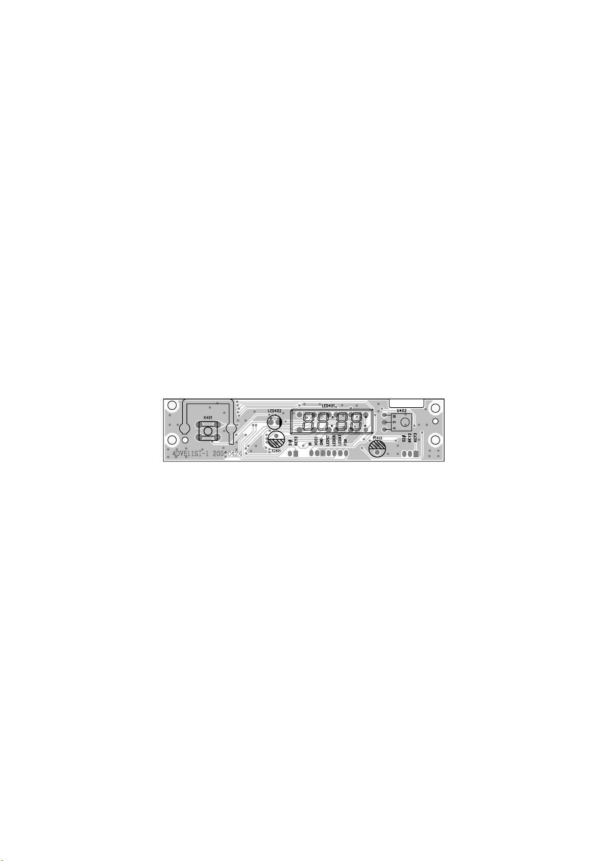
S1#
KEY2
XS403
Main panel
4DV511SI-1
XS402
KEY3
KEY2
S2#
Subsidiary panel (2)
BDV511SI-0
SL-
SP-
SL+
SP+
GND
TRIN#
LOAD-
LOAD+
TROUT#
GND
LIMIT#
FC-
TK+
FC+
XS307 XS306 XS301
FSO
VSDA
VSCK
XS201
Decode board
2DV983A-2
VSTB
GND
VCC
IR
Xs203
-9V
+9V
GND
VCC
CN501
AC220V
Power board
5317SI-1
F
B
GND
XS205
_9V
E
V20
AVCC
+9V
MDI
HFM
CD-LD
VR-CD
GND
VR-DVD
DVD-LD
GND-LD
VIDEO_R/V
VIDEO_G/Y
XS206
VIDEO_B/A
OKA
DET
HSYNC#
VSYNC#
SPDIF
VCC
GND
GND
POATO
VIDEO#
+9V
L#
R#
PDAT2
PDAT1
SPDIF
VCC
Pr
VGND
Y1
VGND
Pb
PDATO
VIDEO#
+10V
L
R
AV board
7231-0
XS701
- 2 -
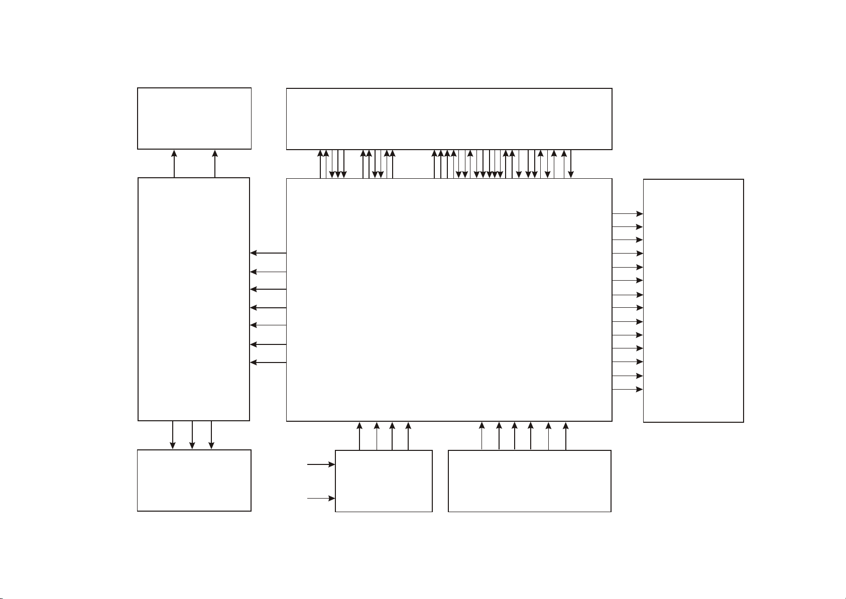
Figure 1.2.1.1 PCB board composition diagram of the player
A
C
D
TK-
IOA
RFO
VCC
XS601
MIC board
6DV511SI-0
1.2.1 PCB board composition diagram of the player
PCB board composition diagram of the player is shown in the figure 1.2.1.1:
Page 4
Output terminal
SY
L
R
LS
RS
Audio
amplifying
filtering
U209
AL
AR
ALS
ARS
VR-DVD
CD/DVD
VR-CD
VR-DVD
Loader
TK-
FC-
FC+
Feed electric machine
Main axis
electric
machine
Open/close
circuit
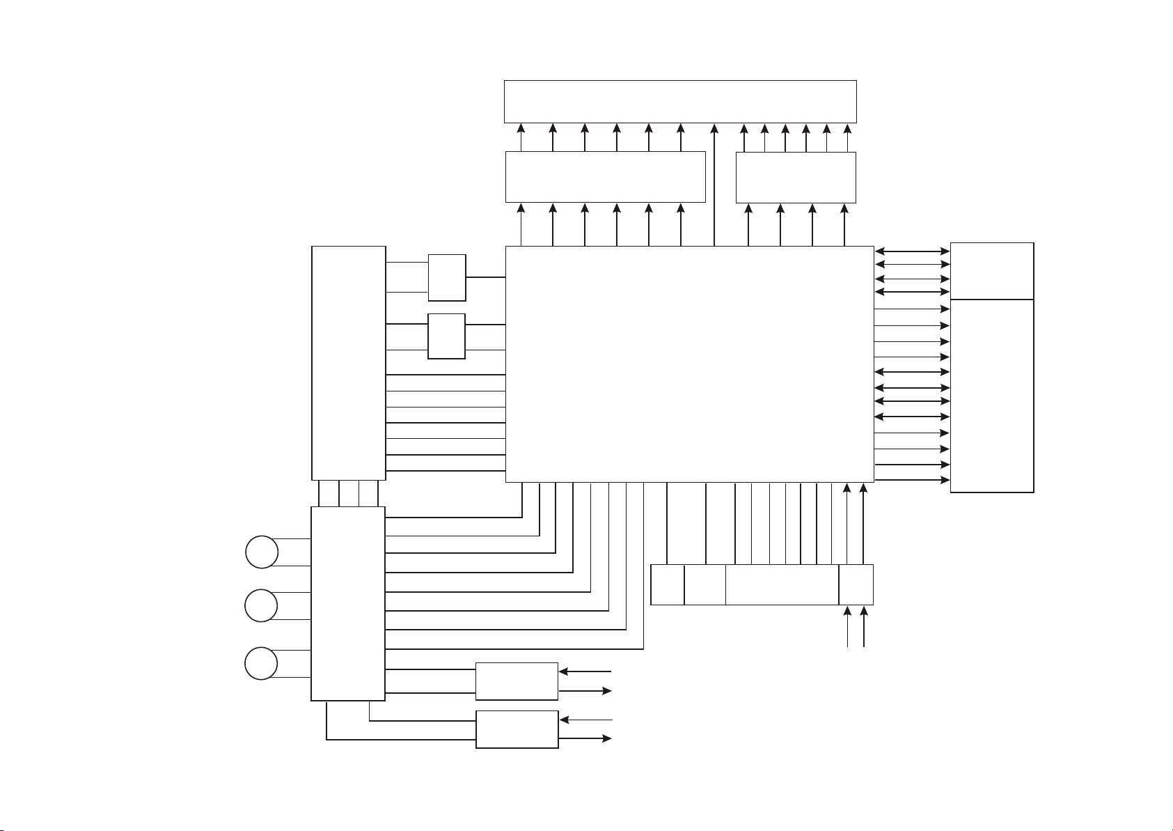
1.2.2 Block diagram of the player
Block diagram of the player is shown in the figure 1.2.2.1:
M
M
M
SL+
SL-
SP+
SP-
LOUD+
LOUD+
TK+
U301 Am58885
Switch
Laser
power
VR-CD
control
MDI
DVD:A/B/C/D/RFO
CD:A/B/C/D/E/F
V20
TRIN
TROUT
LIMIT
VIP4
STBY
FOSO
FMSO
DMSO
TRSO
TROPEN
TRCLOSE
TR_B1
REG01
TR_B2
REG02
IOA
LD02
LD01
Voltage drop
circuit
Voltage drop
circuit
VCC
3.3V
VCC
1.8V
C
SC
U210
U211
SW
CTR
ASPOIF
U201
MT1389
SCL
URST
U202
Reset
24C02
circuit
SC
CVBS
Video
Y/a
CVBS
IR
SDA
VSDA
VSCK
Panel, remote
control receiver
B/a
filtering
VSTB
a/Y
R/V
clamping
CB/B
CR/R
A[0-20]
AD[0-8]
CS#
RAS#
CAS#
WE#
DQ[0-15]
MA[0-11]
BA0
BA1
DCLK
DCKE
IR
FSO
U207
FLASH
SDRAM
U208
- 3 -
Figure 1.2.2.1 Block diagram of the player
MIC
MIC1
MIC2
Page 5
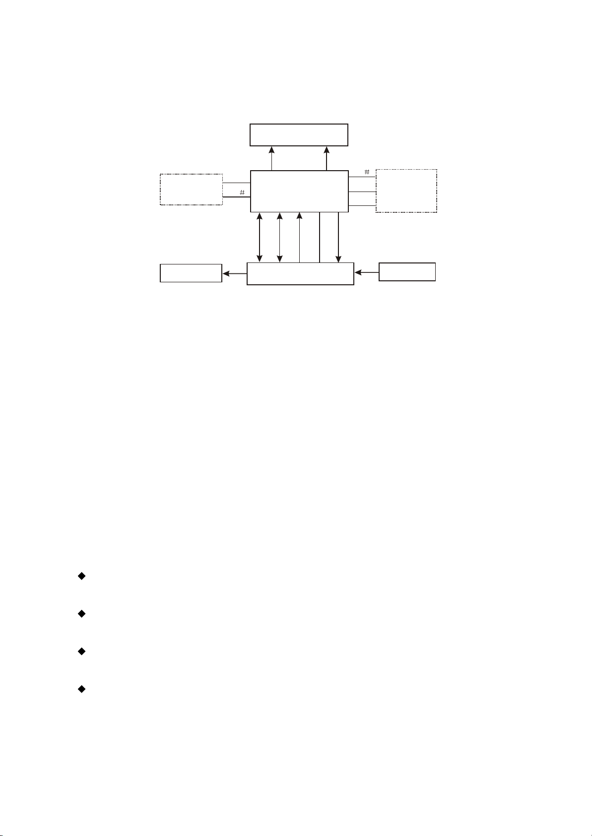
1.3.1 Panel control circuit
1. Panel control circuit block diagram is shown in the figure 1.3.1.1:
LED
S2
Subsidiary
KEY2
KEY3
VCC1
BDV511SI-0
IR
Remote control
receiver
panel 2
Subsidiary
panel1
9DV511SE-0
Indicator light
control circuit
Figure 1.3.1.1 panel control circuit block diagram
KEY2
S1
Fs0
LEDAT
PT6961
LEDST
LEDCK
XS401
GND
2. Working principle
(1) Button function realization: when users are operating the machine, button matrix circuit will
produce a button function code that transmits to the main CPU inside decode chip, CPU performs the
corresponding switch to the function module inside system, and a signal will produce at the same time to
control OSD and panel display part to make the relevant display.
(2) Panel display drive: when the serial data signals sent by decode ship are transmitting to panel
IC (PT6961), IC performs LED drive according to the information send from decode and displays the
relevant content (controlled by software).
(3) Door indicator light control: controlled by decode chip directly.
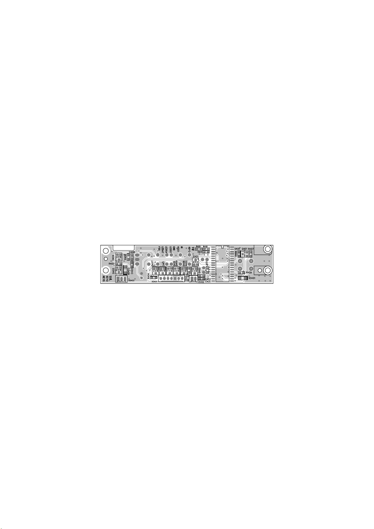
3. Definition and function of main jack of panel
XS402 is connected to subsidiary panel, with the function of transmitting button control signal
and power indicator light control drive voltage.
XS401 is connected to decode board and the jack that communicates with decode system, in
which IR is remote control signal output pin, +5V is panel power supply.
LEDAT is data transmission pin (dual direction), controlled through LEDST, LEDCK is the
working clock signal input displayed by panel.
FSO is the control pin to panel light by firmware.
- 4 -
Page 6
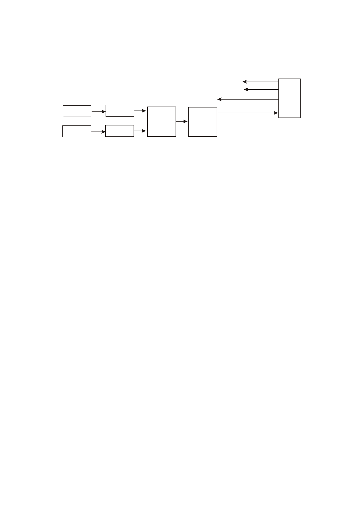
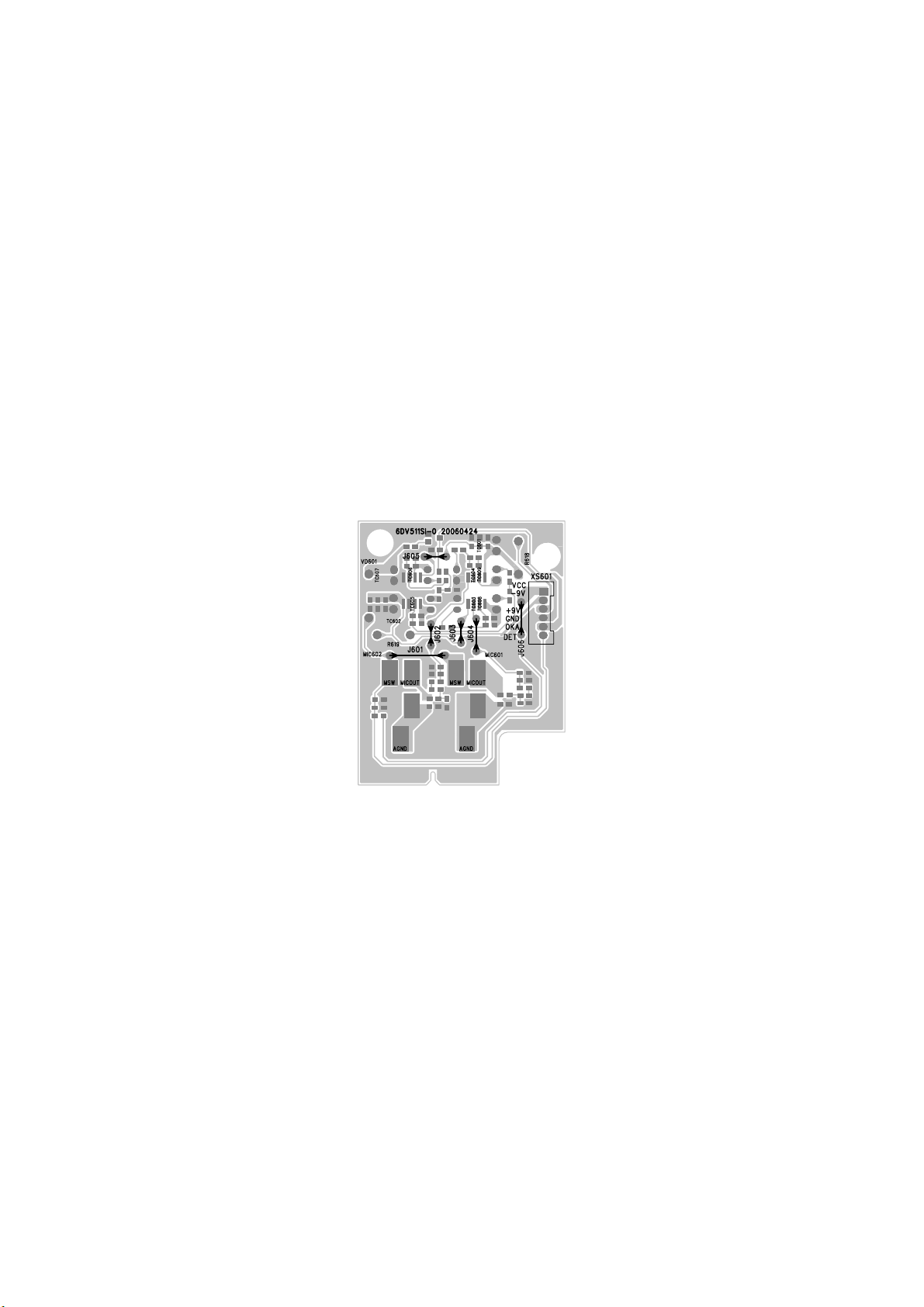
1.3.2 MIC circuit
1. MIC circuit block diagram is shown in the figure 1.3.2.1:
+5V
-9V
MIC1
MIC2
U601A
amplifying
U601B
amplifying
TO MPEG
U602A
amplifying
Figure 1.3.2.1 MIC circuit block diagram
U602B
amplifying
+9V
OK
XS601
2. Working principle
MIC part working principle: after microphone is inserted into MIC left, DET signal on socket changes
from high level to low level to make the mute circuit of decode part and MIC board turn off, no matter
disc reading is available, audio circuit may output normally. If this signal has trouble, microphone will
have no sound when playback pauses. The two-way signals inputted by microphone, after being filtered,
input to pin 3, 5 of U601 separately, and signals after being amplified output from pin 1, 7 of U601. MIC
signals, after U602A mixed amplifying and U602B amplifying again, are outputted by pin 7 of U602 to
decode board for Karaoke signals processing and outputting together with audio signals to fulfill
Karaoke function.
After microphone is unplugged, DET signal changes from low level to high level, Q601 is saturated
on, OK signal is short circuited to ground to prevent interfering rear stage audio output circuit.
- 5 -
Page 7
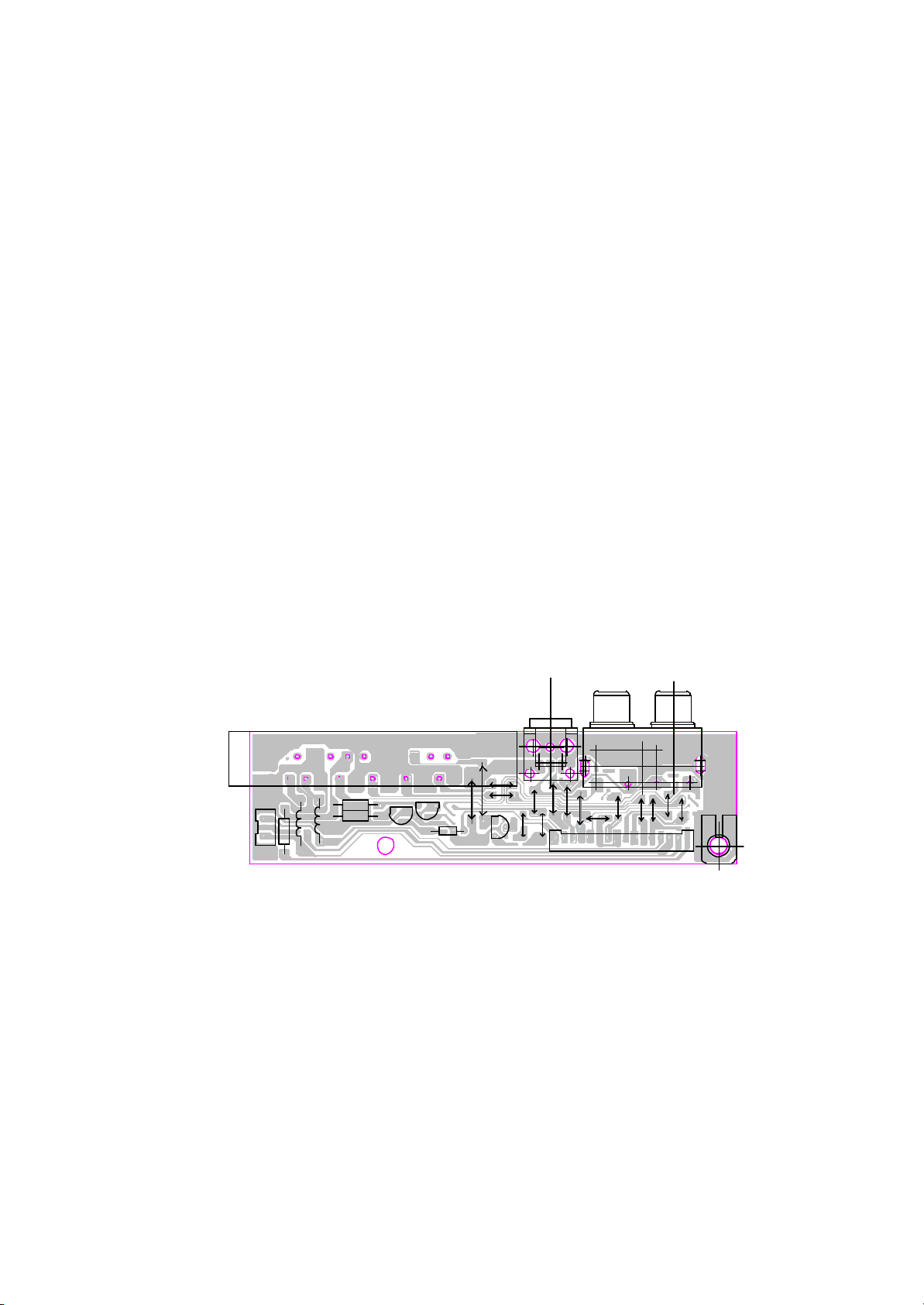
1.4.1 PCB board
1. Surface layer of AV Board
JK706
XS702
R709
L713
R708
R711
L714
7231-0
DVD 2006/1/17
V703
V702
R712
LEI
JP702
JP709
V701
JP721
JP722
JP712
JK705
JP724
JP723
JP720
XS701
PDAT2
PDAT1
JP718
SPDIF
VCC
JK702
JP704
JP728
PR
VGND
JP729
R
G702
+10V
JP727
JP719
JP726
JP725
PB
(PD)
VGND
VIEDOLPDAT0
Y1
VGND
AGND
- 6 -
Page 8
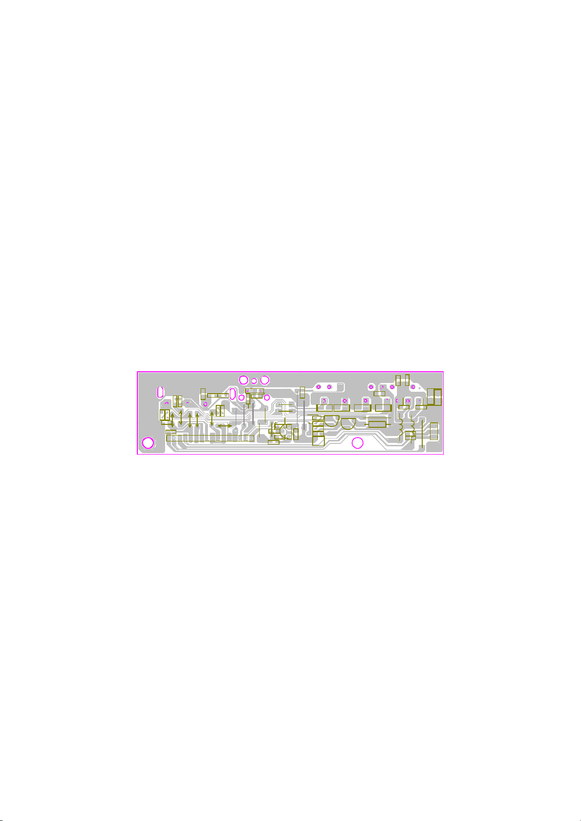
2. Bottom layer of AV Board
C710
L707
R702
R701
C720
L709
L708
R717
C717
C722
R721
R703
C711
R706
R714
C727
R705
R715
ZD704
R704
R710
C716
C723
C724
C728
R713
R716
D701
D702
C725
C726
ZD701ZD702ZD703
R718
R719
- 7 -
Page 9
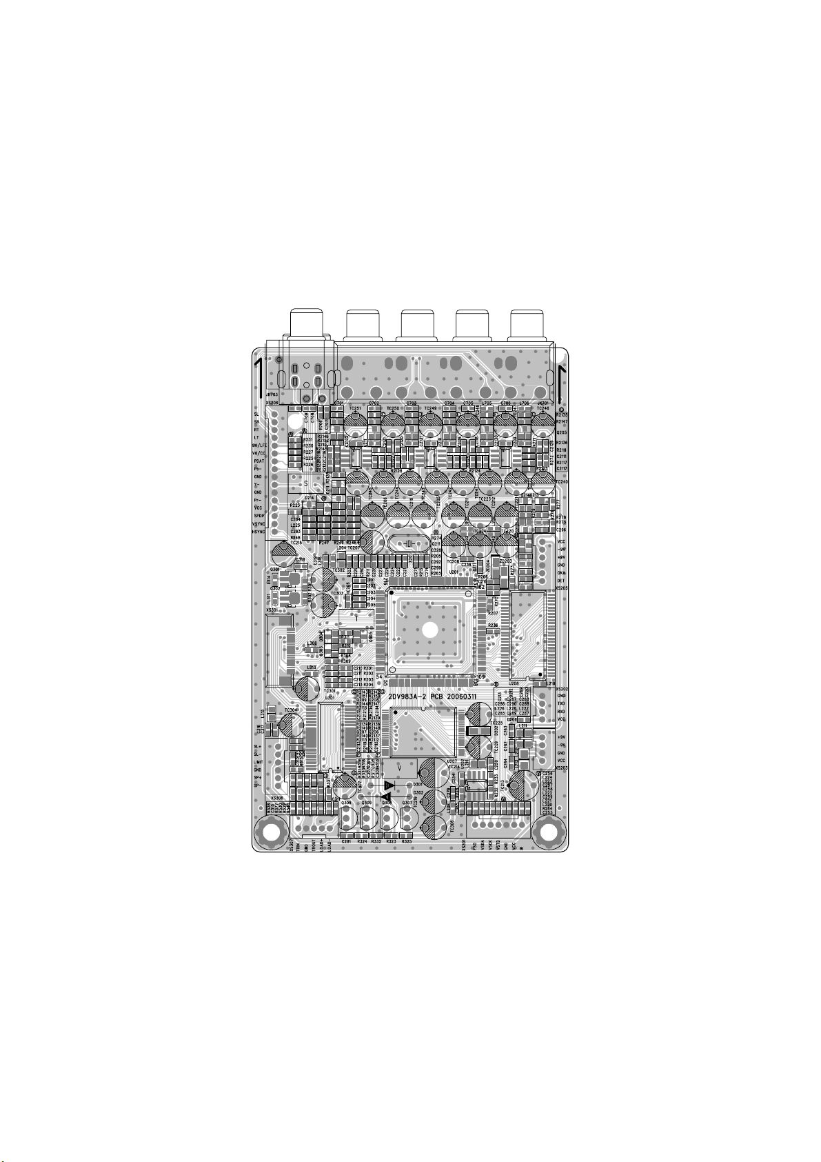
3. Surface layer of DECODE&SERVO Board
- 8 -
Page 10
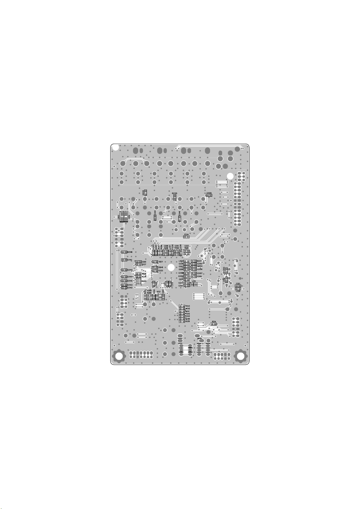
4. Bottom layer of DECODE&SERVO Board
- 9 -
Page 11
5. Surface layer of KEY SCAN Board
- 10 -
Page 12
6. Bottom layer of KEY SCAN Board
- 11 -
Page 13
7. MIC Board
- 12 -
Page 14
U208
R228
510R
SDRAM 64M
23
A0
24
A1
25
A2
26
A3
29
A4
30
A5
31
A6
32
A7
33
A8
34
A9
22
A10/AP
35
A11
20
BA0/A13
21
BA1/A12
38
CLK
37
CKE
19
/CS
18
/RAS
17
/CAS
16
/WE
15
DQML
39
DQMH
36
NC
40
NC
54
VSS
41
VSS
28
VSS
L216
89V33
FB
DQ0
DQ1
DQ2
DQ3
DQ4
DQ5
DQ6
DQ7
DQ8
DQ9
DQ10
DQ11
DQ12
DQ13
DQ14
DQ15
VCCQ
VCCQ
VCCQ
VCCQ
VSSQ
VSSQ
VSSQ
VSSQ
2
DQ7
4
DQ6
5
DQ5
7
DQ4
8
DQ3
10
DQ2
11
DQ1
13
DQ0
42
DQ8
44
DQ9
45
DQ10
47
DQ11
48
DQ12
50
DQ13
51
DQ14
53
DQ15
SD33
1
VCC
14
VCC
27
VCC
SD33
3
9
43
49
6
12
46
52
R/Cr
R246
75R
VGND
B/Cb
R247
75R
VGND
G/Y
R249
75R
VGND
CVBS
R248
75R
VGND
C289
47pF
C287
47pF
C283
47pF
C285
47pF
L226
1.8uH
L228
1.8uH
L225
1.8uH
L227
1.8uH
D214
1N4148*2
VCC
R/Cr#
C284
47pF
D213
1N4148*2
VCC
B/Cb#
C286
47pF
B/Cb#
C290
47pF
C288
47pF
VGND
VGND
VIDEO_G/Y
VIDEO_CVBS
VIDEO_SY
VIDEO_R/V
VIDEO_SC
VIDEO_B/U
VGND
VGND
CC
LFE
SL
SR
VCC
Lt
D212
1N4148*2
Rt
VCC
D211
1N4148*2
L705
FB
L706
FB
C701
102(DNS)
C702
102(DNS)
C703
102(DNS)
C704
102(DNS)
C705
102
C706
102
AGND
CC#
LFE#
L#
R#
1
2
3
4
5
6
7
8
9
10
11
12
JK701
AV8-2
WHITE
RED
89V33
U202
C254
104
AT24C02
1
DC/NC
2
RST_/NC
3
WP/RST_
4
VSS
7
6
5
4
3
2
1
XS201
XS07
C257
47pF(DNS) C258
L218
DV33
FBSMT
C2140
104
- 13 -
XS203
XS04/2.0
1
2
3
4
89V33
8
VCC
7
RST/WP
6
R264
FB
C2141
104
5
FBSMT
FBSMT
FBSMT
FBSMT
FBSMT
C259
47pF(DNS)
SD33
C2142
104
SCL
SDA
SCL
SDA
C255
101
L220
L221
L222
L223
L224
47pF(DNS)
L211 FBSMT
L212 FBSMT
L213 FB
L229 FBVCC AVCC
R2321KR233
1K
IR
VCC
GND
VSTB
VSCK
VSDA
FS0
C256
FV33 DV33
101(DNS)
C279
104
C2143
C2144
104(DNS)
104(DNS)
+9V-9V
+9V
-9V
GND
VCC
TC219
47uF/16V
C2145
104(DNS)
VCC
BA1
DCLK
DCKE
CS#
RAS#
CAS#
WE#
C2146
104(DNS)
SDCKE
C295
20pF
R234 33RBA0
R235 33R
R236
R237
4
3
2
1
RN201
33R
L208
FBSMT
DV33
MA0
MA1
MA2
MA3
MA4
MA5
MA6
MA7
MA8
MA9
MA10
MA11
DBA0
DBA1
33R
SDCLK
33R
SDCKE
DCS#
5
DRAS#
6
DCAS#
7
DWE#
8
DQM0
DQM1
1.4.2 circuit diagram
1. DECODE&SERVO Board 1
TC215
47uF/16V(DNS)
XS202
XS04(DNS)
DV33
1N4148
D202
VCC
TC225
47uF/16V
C262
C263
C264
104
104
C267
C268
89V33
RXD
TXD
GND
Q221
104(DNS)
R251
10K
C269
104(DNS)
C261
104(DNS)
R300
33R
C293
104(DNS)
URST#
104(DNS)
VGND
1
2
3
4
1k
R250
R299
2SC1815-YS
10K
C265
104
104
TC213
TC214
220uF/16V
220uF/16V
U207
A20
4.7K
A16
A15
A14
A13
A12
A11
A10
A9
R243 0R
AA20
R245 0R(DNS) A21
PWR#
A19
A18
A8
A7
A6
A5
A4
A3
A2
FV33 A17
R242 4.7K
R240 4.7K
R239 4.7K
R238 4.7K
R241
1*16MBit_FLASH(TSOP)
1
A15
2
A14
3
A13
4
A12
5
A11
6
A10
7
A9
8
A8
9
A19
10
NC
11
WE
12
RESET
13
NC
14
VPP
15
RY/BY
16
A18
17
A17
18
A7
19
A6
20
A5
21
A4
22
A3
23
A2
24
A1
BYTE
DQ15/A-1
DQ14
DQ13
DQ12
DQ11
DQ10
DQ7
DQ6
DQ5
DQ4
DQ3
DQ2
DQ9
DQ1
DQ8
DQ0
A16
Vss
Vcc
OE
Vss
CE
A0
VIDEO_CVBS
R706
2.2R
C707
XS206
XS16
1
2
3
4
5
6
48
47
GND
46
A0
45
AD7
44
43
AD6
42
41
AD5
40
39
AD4
38
FV33
37
36
AD3
35
34
AD2
33
32
AD1
31
30
AD0
29
PRD#
28
GND
27
PCE#
26
A1
25
7
8
9
10
11
12
13
14
15
16
VGND
HSYNC#
VSYNC#
SPDIF
VCC
VIDEO_R/V
GND
VIDEO_G/Y
GND
VIDEO_B/U
R226 75R
L#
R#
SR
SL
DV33
PDAT0
R225 0R
R227 0R(DNS))
R230 0R
R231 0R(DNS)
R229
4.7K
ASDAT3
VIDEO#
CC#
+9V
LFE#
VIDEO_SY
VIDEO_SC
101(NC)
VIDEO#
VGND
101(NC)
VGND
C709
C708
101(NC)
5
6
3
4
JK703B
V-OUT5
7
JK703A
S-VIDEO
1 2
Page 15

VREF
SPDIF
ALRCK
ACLK
ABCK
GPIO5
DVSS
GPIO4
GPIO3
RA11
DVDD3
RCLK
RA10
RCS#
RAS#
CAS#
RWE#
DQM1
DVSS
RD10
RD11
RD12
RD13
RD14
RD15
C276
33pF
FS
RA4
RA5
RA6
RA7
RA8
RA9
CKE
RA3
RA2
RA1
RA0
BA1
BA0
RD8
RD9
RD0
RD1
RD2
RD3
RD4
DACVDD3 89V33
L206
FBSMT
TC212
10uF/16V
4.7K
R270
ASDAT2
R207 1K
ALRCK
R206 560R
FS
C216 104
VREF
R223
75R
89V33 V18
162
161
160
159
158
157
156
155
154
153
152
151
150
149
148
147
146
145
144
143
142
141
140
139
138
137
136
135
-12V
134
133
132
131
130
129
128
127
126
125
124
123
122
121
120
119
118
117
116
115
114
113
112
111
110
109
C242
104
VMUTE
SPDIFIEC958
FS
VREF
DACVDD3
IEC958
AMDAT
ASDAT3
ASDAT2
ASDAT1
ASDAT0
ALRCK
ACLK
ABCK
TROUT
TRIN
LIMIT
MA4
MA5
MA6
MA7
MA8
MA9
MA11
DCKE
DCLK
MA3
MA2
MA1
MA0
MA10
BA1
BA0
CS#
RAS#
CAS#
WE#
DQM1
DQ8
DQ9
DQ10
DQ11
DQ12
DQ13
DQ14
DQ15
DQ0
DQ1
DQ2
DQ3
DQ4
2. DECODE&SERVO Board 2
C243
104
AVCC
2SK3018-S
R329
10K
R340 330R
R377 330R
C311
103
Q304
4.7uH
FBSMT
4.7uH
FBSMT
1R
Q305
3904-S
R309
10K
R311
10K
R310
100K
U301
15
VOTK+
16
VOTK-
17
VOLD+
18
VOLD-
19
VCC2
20
NC
21
PVCC
30
GND2
22
PREGND
23
VINLD
24
NC
25
TR_B2
26
VINTK
27
BIAS
MUTE28VINFC
AM5888S
DV33
SL+
SL-
LIMIT#
SP+
SP-
R320
150K
R318
680K/1%
TROUT
TRIN
AVCC
R315
330
C301
104
C307 222
R317
680K/1%
IOA
MDI
E
V20
F
B
A
RFO
IOA
D
C
TKTK+
FC+
FC-
VOFC+
VOFC-
VOSL+
VOSL-
VOTR+
VOTR-
REGO1
VINSL+
REGO2
GND1
TR_B1
TC301
220uF/16V
VCC1
REV
FWD
LIMIT
C309
222
89V33
C308
101(DNS)
R301
4.7R
2SB1132-S
2SB1132-S
R302
4.7R
14
13
12
11
10
9
8
29
7
6
5
4
3
2
1
R331
Q301
0R
Q302
L316
FBSMT
LDO-AV33
LDO-AV33
FCSPSP+
LOAD+
LOADMO-VCC
GND
TRCLOSE
TROPEN
REGO1
REGO2
FOSO
OPOP+
V1P4
TC302
47uF/16V
TC303
47uF/16V
RFVDD3
C237
222
OPO
ADIN
C281
104
LDO-AV33
C318
104
LDO2
LDO1
C238
103
R314
10K
C319
104
C239
104
C316
104
TC307
100uF/16V
PLLVDD3
AADVDD3
C236
104
C246
104(DNS)
L203
FBSMT
C317
104
C247
104(DNS)
MO-VCC
DMSO
Q306
SS8550
C229
104
100uF/16V
R324
5.6K
L201
V18 RFV18
FBSMT
R303
10R
TC207
100uF/16V
L202
4.7uH
TC208
220uF/16V
C249
C248
104
104(DNS)
89V33
L204
330uH
L315
FBSMT
TC304
MO-VCC
D302
1N4001
10K
R332
C250
104
VCC
FMSO
TRSO
FOSO
V1P4
C210
153
D301
1N4001
Q309
SS8550(DNS)
C230
104
89V33
89V33
89V33
220uF/16V
ADACVDD3
C240
103
C207
104
C208
104
C209
104
C211
104
12K
R323
1.8V
TC209
TC210
220uF/16V
C2154
105
C2156
105
C2158
105
C212
331
TR_B1TR_B2
SS8550(DNS)
Q308
R201
R202
R203
R204
C213
331
L219
FBSMT
C2155
105
C2157
105
C2159
105
R325
20K
Q307
SS8550
REGO1REGO2
V18
C
B
A
D
RFO
C206
101
C214
104
10KDMSO
15K
27K
27K
C231
C232
104
104
C201 105
C202 105
C203 105
C204 105
C205 105(DNS)
C
B
A
D
SUBA
SUBB
SUBC
SUBD
E
F
MDI
LDO2
LDO1
RFOP
RFON
V2P8
V20
V1P4
FEO
TEO
TEZISLV
OPO
OPOP+
DMO
FMO
TROPEN
V1P4_IN
TRO
FOO
ADIN
VSYNC#
HSYNC#
STBY
A2
A3
A4
A5
A6
A7
A8
TR_B1TR_B2
DV331.8V
TC306
100uF/16V
RFVDD3
V18
C233
104(DNS)
C260
104
R211
15K
C234
104(DNS)
10
11
12
13
14
15
16
17
18
19
20
21
22
23
24
25
26
27
28
29
30
31
32
33
34
35
36
37
38
39
40
41
42
43
44
45
46
47
48
49
50
51
52
53
54
C228
RFVDD3
1
AGND
2
DVDA
3
DVDB
4
DVDC
5
DVDD
6
DVDRFIP
7
DVDRFIN
8
MA
9
MB
MC
MD
SA
SB
SC
SD
CDFON
CDFOP
TNI
TPI
MDI1
MDI2
LDO2
LDO1
SVDD3
CSO/RFOP
RFLVL/RFON
SGND
V2REFO
V20
VREFO
FEO
TEO
TEZISLV
OP_OUT
OP_INN
OP_INP
DMO
FMO
TROPENPWM
PWMOUT1/ADIN0
TRO
FOO
FG/ADIN1
GPIO0/VSYNC#
GPIO1/HSYNC#
GPIO2
IOA2
DVDD18
IOA3
IOA4
IOA5
IOA6
IOA7
HIGHA0
89V33
APLLVDD3 89V33
TC205
10uF/16V
89_SW
89_AR
89_ARS
184
182
181
183
ARS
ARF(SW)
AR/SDATA1
VSCK
IOA
L205
4.7uH
C241
104
180
179
178
APLLVSS
ADACVSS2
ADACVSS1
VSDA
VSTB
SCL
C218
152
APLLVDD3
AADVDD3
177
176
AADVDD
APLLCAP
APLLVDD
95
SDA
FS0
C217
104
MIC_IN1
MIC_IN2
ADVCM
175
173
174
AKIN1
ADVCM
UP3_196UP3_4
97
MIC_DET
RXD
TXD
R/Cr
171
172
AKIN2
AADVSS
R/Cr/CVBS/SY
UP3_598GPIO799ICE
100
TRCLOSE
ICE
TC204
10uF/16V
B/Cb
170
B/Cb/SC
PRST#
101IR102
URST#
C219 391
JITFNJITFO
V1P4
OSP
211
RFGND
DVDD360HIGHA7
C224
102
210
209
CRTPLP
61
A14
A13
208
207
HRFZC
RFRPAC
HIGHA562HIGHA6
HIGHA4
64
63
A12
A11A9A20
C223
20pF
RFVDD3
205
206
RFRPDC
RFVDD3
HIGHA265HIGHA3
A10
473
C222
204
203
202
LPFOP
ADCVSS
ADCVDD3
HIGHA166IOCS#
IOA20
68
69
67
PCE#A1AD0
C220
C221
201
LPFIN
IOA1
70
PRD#
474
473
200
LPFIP
IOOE#
71
PLLVDD3
199
LPFON
PLLVDD3
AD1
R210
100K
104
333
C225
C226
C227
104
104
212
213
216
215
214
OSN
IREF
RFGC
AVDD3
A16
IOA18
IOWR#
IOA19
59
58
55
57
56
A18
A19
PWR#
A16
A15
JITFN
198
197
196
PLLVSS
IDACEXLP
DVSS74AD273AD172AD0
75
AD2
AD3
JITFO
195
JITFN
AD3
76
AD4
TC206
10uF/16V
194
193
JITFO
XTALI
AD577AD4
AD5
AD6
R209 750K
RFV18XIXO
191
192
XTALO
RFVDD18
U201
MT1389E
LQFP216/SMD
AD678IOA21
80
79
ALE
A21
A21
FS0
TC211
100uF/16V
89_AL
89_ALS
89_CTR
ADACVDD3
190
185
186
188
189
187
AVCM
RFGND18
ALF(CTR)
ADACVDD2
ADACVDD1
AL/SDATA2
ALS/SDATA0
AD7
IOA0
A17
ALE
DVDD1884UWR#85URD#86DVDD387UP1_288UP1_389GPIO690UP1_491UP1_592UP1_693UP1_794UP3_0
81
83
82
A17A0URD#
UWR#
AD7
V18
R215 100K
XI XO
X201
C275
27MHz
33pF
G/Y
CVBS
DACVDD3
164
169
168
167
166
165
163
CVBS
DACVSSA
DACVSSB
DACVSSC
DACVDDA
DACVDDB
G/Y/SY/CVBS
DACVDDC
MC_DATA
ASDATA3
ASDATA2
ASDATA1
ASDATA0
DVDD18
DVDD18
RD6
INT0#
DQM0
RD7
RD5
DVDD3
106
103
104
105
107
108
INT0#
DQM0
DQ7
DQ6
DQ5
IR
R308
100K
Q303
XS301
2SK3018-S
24P0.5mm
24
GND-LD
23
L314
DVD-LD
22
21
L313
HMF
20
19
CD-LD
L311
18
VR-DVD
17
VR-CD
16
15
14
L308
13
12
11
10
9
8
7
6
5
4
3
2
1
C303
C302
104
104
TK- FC+
TK+
SL+
MO-VCC
- 14 -
C305
104
R313 10K
1
2
3
XS306
4
5
6P2.0mm
6
XS307
5P 2.0mm
1
LOAD-
2
LOAD+
3
TROUT#
4
5
TRIN#
SL-
C304
C306
104
104
FMSO
TR_B2
TRSO
V1P4 TR_B1
STBY
R328 10K
C313 104
R321
R319
150K
DV33
R330
10K
GND
C310
103
Page 16

3. DECODE&SERVO Board 3
+9V
Q211
1015
C2130
104(DNS)
AGND
-9V
C2133
104(DNS)
AGND
102(DNS)
473
C298
C299
1
2
3
4
5
6
C328
101
R278
VCC
1K
R274
1K
10K
R276
10K
AGND
30K
R2111
C2111 100pF
1
7
7
1
7
+A9V
-A9V
+A9V
-A9V
1
+A9V
-A9V
R2112
C2112 100pF
+A9V
-A9V
C2113 150pF
+A9V
-A9V
C2114 150pF
U210A
4 8
4580
R2115
C2115 150pF
U211B
4 8
4580
R2116
C2116 150pF
+A9V
-A9V
4 8
R2135
Q205
2SC1815-YS
Q206
2SC1815-YS
Q207
2SC1815-YS
Q208
2SC1815-YS
Q209
2SC1815-YS
2SC1815-YS
1K
R2136
1K
R2137
1K
R2138
1K
R2139
1K
R2140
1K
R2141
1K
R2142
1K
R2143
1K
R2144
1K
R2145
1K
R2146
1K
Rt
R2147
100K
AGND
R2148
100K
Lt
SR
R2149
100K
AGND
SL
LFE
Cc
R2150
100K
R2151
100K
R2152
100K Q210
- 15 -
MUTE-1
MUTE-1
MUTE-1
CH-R
CH-L
CH-SR
CH-SL
CH-SW
CH-C
TC246
10uF/16V
TC247
10uF/16V
TC248
10uF/1206
TC249
10uF/1206
TC250
10uF/1206
TC251
10uF/1206
U209B
4 8
4580
U209A
4 8
4580
R2113
U210B
4 8
4580
R2114
2
3
6
5
U211A
4580
R2117
4.7K
6
5
30K
30K
30K
2
3
AGND
R2118
4.7K
2
3
AGND
30K
R2119
4.7K
6
5
AGND
30K
R2120
4.7K
AGND
R2121
R2127
4.7K
10K
C2121
102
AGND
R2122
R2128
4.7K
10K
C2122
102
AGND
R271
36K(NC)
R2123
10K
C2117
102
R272
36K(NC)
R2124
10K
C2118
102
DV521SI使用以下音频放大输出电路
R2125
10K
C2119
102
R2126
10K
C2120
102
OKA
AGND
R
L
SR#
SL#
SW
CTR
C2129
102(DNS)
10uF/16V
10uF/16V
R205
0R
TC240
10uF/16V
TC241
10uF/16V
TC242
10uF/16V
TC243
10uF/16V
TC244
TC245
OK
89_AR
89_AL
89_ARS
89_ALS
89_SW
89_CTR
VMUTE
R273
100K
89V33AGND
MIC_DET
MIC_IN1
MIC_IN2
473
C297
DET
OK
GND
+9V
-9V
VCC
TC220
100uF/16V
-9V
C2131
104(DNS)
C2134
104(DNS)
XS205
2.0mm
C296
105(DNS)
C2132
104(DNS)
C2135
104(DNS)
R265 330R
R266
R267 0R
Q213
1015
Q212
2SC1815-YS
AGND
R277
10K
TC222
100uF/16V(DNS)
TC223
100uF/16V(DNS)
0R
C292
OK OKA#
105
MUTE-1
D203
1N4148
-12V
DET
OKA#
OKA#
Q214
1015
89V33
AGND
ZD203
3V/0.5W
ZD204
2.7V/0.5W
AGNDR275
R279
10K
D204
1N4148
TC221
100uF/16V
VCC
Page 17

4. KEY SCAN Board
R409
330
VCC
R406
470(DNS)
Q401
8050(DNS)
LED01
LED401
RED LED
R411
U402
HS0038B3V
123
G13
R405
100R
-12V
TC402
C403
100uF/16V
104
0R
R410
0R
XS403
1
2
3
XS03/2.0
VCC VCC
R408
10K
IR
C408
102
VCC1
XS402
XS02/2.0
U401
1
OSC
2
DOUT
3
DIN
4
CLK
5
STB
6
K1
7
K2
8
K3
9
VDD
10
SEG1/KS1
11
SEG2/KS2
12
SEG3/KS3
13
NC
14
SEG4/KS4
15
SEG5/KS5
SEG6/KS616SEG7/KS7
PT6961
LEDST
D409
1N4148-SE(DNS)
KEY2
KEY3
VCC
SEG12/GR7
SEG10/KS10
SEG9/KS9
SEG8/KS8
1N4148-SE(DNS)
32
GND
31
GR1
30
GR2
29
GND
28
GR3
27
GR4
26
GND
25
VDD
24
GR5
23
GR6
22
21
SEG11
20
19
18
17
TC401
100uF/16V
Play/Pause
K402
K403
Stop
VCC
LEDCK LEDAT
D410
LED401
7 6
G8
8
G9
9
S10
10
S11
11
G12
LED-SOCK(1)
KEY2
S1#
S2#
KEY2
KEY3
1
2
1
2
3
XS402
XS02/2.0
XS403
XS03/2.0
- 16 -
VCC
R402
R403
R404
10K
10K
10K
5
4
3
2
112
IR
VCC1
GND
LEDST
LEDCK
LEDAT
FS0
G6S7
S5
S4
S3
S2
S1
S1
VD401
1N4148
S1#
1
2
3
4
5
6
7
XS401
*
S2
S2#
VD402
1N4148
VCC
ON/OFF
C401
104
KA01
S1#
R401 51K
K401
Open/Close
KEY2
LEDAT
LEDCK
LEDST
KEY1
KEY2
KEY3
S1
S2
S3
S4
S5
1
S1#
2
L401
VCC
S2#
D411
1N4148-SE(DNS)
G12
G9
G8
G6
G14
G13
LED
S10
S11
S7
VCC
C402
104
S2#
KEY2
KEY3
R407
FS0
1K(DNS)
KEY1
D401
1N4148-SE(DNS)
VCC
KEY2
D402
1N4148-SE(DNS)
KEY3
D403
1N4148-SE(DNS)
S1
D404
1N4148-SE(DNS)
FS0
D407
1N4148-SE(DNS)
VCC
IR
D406
1N4148-SE(DNS)
Page 18

5. MIC Board
R609 10K
R607
1K
R608
1K
R605
5.1K
R606
5.1K
6
5
C614 101
-9VA
2
3
+9VA
R610
10K
C615 101
8 4
U601B
4558
U601A
4558
R613
10K
TC608
10uF/16V
TC609
10uF/16V
R611
5.1K
R612
5.1K
1
7
C618 101
-9VA
2
3
+9VA
TC605
R624
10uF/16V
5.1K
1
U602A
4558
8 4
VCC
-9V
+9V
GND
OKA
DET
C619
102
1
2
3
4
5
6
R614
5.1K
XS601
XS601
R615
10K
C621 101
6
5
U602B
4558
OKA
TC606
10uF/16V
R616
7
1K
C623
102
VD601
DET
A1K
1N4148插件
R618
33R/0.25W
+9V +9VA
TC601
100uF/16V
R619
33R/0.25W
-9V -9VA
TC602
100uF/16V
R623
1K
B
2
TC607
10uF/16V
C602
C601
104
104
C605
C604
104
104
C603
104
C606
104
-12V
CE
Q601
2SC1815
TC603
10uF/16V
C610
L602
105
C609
103
R601
10K
C611
105
R602
10K
R603
560R
TC604
10uF/16V
R604
560R
C613
103
C612
103
L604
FBSMT
FBSMT
L601
FB
L603
R621
12K
FB
4
3MIC601
CK3-6.35-24
- 17 -
MIC602
CK3-6.35-24
2
1
VCC
R620
5.1K
DET
Page 19

6. AV Board
VCC
JP724
0R
R706
75R
C723
102
+10V
AGND
AGND
R709
330R
R708
33R
V702
8050
R711
1K
V703
8050
AV_TV
R705
47K
AGND
L713
L714 FCM
AGND
ZD704
5.1V/0.5W
C726
104
FCM
ZD701
5.1V/0.5W
ZD702
5.1V/0.5W
ZD703
5.1V/0.5W
R714
2.2K
JP712
0R
R#
Pb#
Y1#
Pr#
VIEDO#
PDAT1
SCART 8PIN 9.5V-12V AV 4:3
SCART 8PIN 5.0V-8.0V AV 16:9
SCART 8PIN 0.0V-2.0V TV MODE
VCC
JP724
0R
R704
4.7K
PDAT0
R#
AGND
L#
PDAT2
XS702
1
2
3
XS3
- 18 -
R710
2.2K
R712
2.2K
C724
102
SCART 16PIN 0 CVBS MODE
SCART 16PIN 1 RGB MODE
R716
0R
R713
0R
AGND VGND
D701
D702
IN4148
IN4148
SPDIF
AGNDVGND
VGND VGND
JP718
0R
JP720
0R
JP720
0R
R703
68R
VGND
V701
8050
VGND
VCC
VGND
VGND
PDAT0
PDAT0
+10V
AGND
R#
G
R701
220R
R702
JP702
0R
CONT
V-IN
NC
JK705
OPTICAL
1
2
3
2
4
6
8
10
12
14
16
18
20
VIN
VCC
GND
R715
47K
AV_TV
VGND
C716
C727
102
102
AGND
C725
104
JK706
1
A(B)OUT
A(B)IN
3
A(A)OUT
A-COM
5
RETURN
A(A)IN
7
BLUE I/O
FUNC SW
9
RETURN
11
GREEN I/O
13
RETURN
RETURN
15
RED I/O
BLK I/O
17
RETURN
TRTURN
19
V-OUT
21
GND
VJS3921
VCC
C711
104
C728
104
RGB_CVBS
AGND
RGB_CVBS
SPDIF
Pb
Pr
Y1
C720 0R
C710 104
C717 0R
C722 0R
B
R
100R
R721
JP729
JP725
R717
R718
R719
L709
FBSMT
L707
FBSMT
L708
FBSMT
JP704
0R
JP728
0R
0R(DNS)
0R
0R(DNS)
0R
0R
0R(DNS)
Y1#
Pb#
Pr#
VGND
PDAT2
PDAT1
SPDIF
Pr
VGND
Y1
VGND
Pb
VIEDO#
L#
R#
+10VL#
from 解码板
JP719
0R
JP726
0R
JK702
1
3
4
6
RCA-407
1
2
3
XS701
4
XS16
5
6
7
8
9
10
11
12
13
14
15
16
GREEN
2
-12V
BLACK
BLUE
5
RED
Page 20

7. POWER Board
D512
HER105(DNS)
TC508
220uF/50V(DNS)
C507
104(DNS)
!
TC504
TC501
22uF/400V
L503
D6D7D
Vstr5VCC
Ipk
FB
R503
39K/2W
8
Vfb
Gnd
1
C503
101/1KV(DNS)
2
BC501
~275V 104
BCN501
~220V
2
D504
1N4007
1
D503
1N4007
R518
180K 2W
*
*
*
*
*
*
R501
*
680K 2W
*
*
*
!
*
*
*
F501
T1.6A/250V
*
*
*
*
4
R512
10K(NC)
D502
1N4007
D501
1N4007
L501
- 19 -
!
!
!
BCN503
SW-SPST
U501
FSDH321
3
JP502
0R
C502
103/1KV
C505
104
D505
HER107
C506
223
R505
150R
TC502
47uF/50V
D506
HER107
!
!
T501
1
3
4
5
EEL19H
!
U502
HS817
BC503
~400V 221
BC504
~400V 221
12
11
10
C516
9
8
7
6
HER105(DNS)
D513
D510
SR560
152
JP504
0R
R506
330R
L507 10uH/2A
TC505
1000uF/10V
U503
LM431A
100uF/16V(DNS)
R507
1K
K
R
A
TC506
1000uF/10V
R502
0R
C508
104(DNS)
C510
104
C515
104
R509
10K
JP504
0R
R508
10K
D507
+5V
1N4007(DNS)
D508
D511
HER105
+5V +3.3V
ZD501
5.1V(DNS)
R510
4.7K(DNS)
D509
1N4007(DNS)
HER105
Vin3Vout
U504
-21V
FLFL+
TC507
220uF/16V(DNS)
TC503
220uF/16V
TC509
220uF/16V
AZ1086(DNS)
ADJ/GND
1
+9V
-9V
+3.3V
C511
104(DNS)
2
R515
120R(DNS)
R516
200R(DNS)
+5V
GND
-21V
FLFL+
CN502
1
2
3
4
5
XS05/2.0(DNS)
1
2
3
4
5
6
CN501
XS06/2.0
-12V
+9V
-9V
GND
JP505
+5V
GND
0R
+3.3V
BCN502
~220V
BC505
1
2
!
~400V 221
Page 21

DV514SI-2 Service Manual
2.1.1 Block diagram of the player
DV514SI 2 adopts the outlook of DV514SI, and adopts the solution of DV317 series on the basis of DV514,
with the function similar to DV514SI. Decode board adds 5.1CH output on the basis of DV317SI, power board and
AV board are the same with those of DV317SI, only headphone signal socket is deleted on AV board. Panel, MIC
board and subsidiary board are the same with those of DV514SI. For working principle of each unit circuit of this
player, please refer to “DV317SI Service Manual”. Block diagram of the player is shown in the figure 2.1.1.1:
PICK-UP
Feed
electric
machine
Main
axis
electric
machine
ACIN
VR-DVD
VD-CD
LD-DVD
LD-CD
TK-
TK+
FC+
FC-
SL+
M
M
M
Power
board
CD/DVD switch
Laser power
control
DVD:A/B/C/D/RFO
CD:A/B/C/D/E/FRFO
AM5888
TRB1
U301
TRB2
REGO1
Voltage
regulating
circuit
SL-
SP+
SP-
SDRAM 64M
U208
Ld02
Ld01
MDI
VIP4
FOSO
FMSO
DMSO
TRSO
REGO2
V18
Dv33
+9V
IOA
FLASH16M
U207
MT1389 E
U201
UREST
Reset
Panel
MIC board
XI
SDA
SCL
27M clock
EEPROM
U202
24C02
XO
AL
AR
ALS
ARS
CTR
SW
CVBS
Y/G
CB/B
CR/R
MIC1
MIC2
Audio
amplifying
filtering
U209
Video
filtering
catching
L
R
SL
SR
CC
FFT
SY
SC
CVBS
B/U
R/V
G/Y
Audio
output
terminal
S-video
Video
output
L#
R#
SPDIF
AV output board
VIEDO#
PB#
PR#
Y#
-9V
Figure 2.1.1.1 Block diagram of the player
- 20 -
Page 22

Power board
5317SI-1
CN501
+9V
-9V
GND
VCC
Loader frame Small bracket
FC-
FC+
TK+
TK-CD
SL+
SL-
LIMIT#
GND
SP+
LOAD-
LOAD+
TROUT
GND
TRIN
GND
TRIN#
LOAD-
LOAD+
TROUT#
SP-
SL-
SP-
SL+
SP+
GND
LIMIT#
FC-
IOA
C
D
TK-
IOA
TK+
FC+
XS307 XS306 XS301
Decode board
2DV983A-2
Laser head
RFO
ABF
GND
F
A
B
RFO
GND
V20
AVCCEVR-CD
V20
VR-DVD
CD-LD
MDI
HFM
DVD-LD
GND-LD
E
MDI
AVCC
HFM
CD-LD
VR-CD
DVD-LD
VR-DVD
XS206
GND-LD
HSYNC#
VSYNC#
VIDEO_R/V
VIDEO_G/Y
VIDEO_B/A
POATO
VIDEO#
SPDIF
VCC
GND
GND
+9V
1
2
3
4
5
6
7
8
9
10
11
12
13
L#
14
R#
PDAT2
PDAT1
SPDIF
VCC
Pr
VGND
Y1
VGND
Pb
PDATO
VIDEO#
+10V
L
R
AV board
7231-0
XS701
- 21 -
Figure 2.1.2.1 PCB board block diagram of the player
SDA
DATE
Xs201
SCK
STB
GND
STB
CLOCK
XS401
VCC
IR
IR
+5V
GND
DETOKGND
+9V
-9V
MIC board
VCC
6975-0
AC220V
Subsidiary
panel
9975-0
2.1.2 PCB board block diagram of the player
PCB board block diagram of the player is shown in the figure 2.1.2.1:
XS901
VCC
GND
POWER_LED
SEG2
KEY1
Main panel
4975-0
XS402
Page 23

2.2.1 PCB board
1. Surface layer of KEY SCAN Board
VGO
LED404
K401
LED403
U402
4975-1
DVD 2004/8/4
R409
LED401
K402K403
LED402
- 22 -
Page 24

2. Bottom layer of KEY SCAN Board
C402
GND1
C403
R403
R402
C401
R401
XS401
L401
L402
C411
GND2
C407
TC401
R408
U401
V401
R412
C406
R410
R411
C405
C408
R406
R407
R405
R414
TC402
D401
DZ401
XS403
C410
R413
D402
C409
- 23 -
Page 25

3. Surface layer of MIC Board
TC611
MIC601
TC613
JP608
TC616
JP606
JP607
TC604
R622
R621
TC615
JP602
L601
JP605
TC603
JP601
AGND
+9V
-9V
+5V
XS601
DET
OK
MIC602
TC605
6975-0
DVD 2004/08/04
TC606
JP603
TC601
L602
JP604
TC602
- 24 -
Page 26

4. Bottom layer of MIC Board
R623
R618
R602
R612
R611
C608
R617
C607
R620
R616
R615
R613
U602
VD601VD602VD603
R619
L604
L603
R604
R606
C604
R601
C602
R603
R610
R608
U601
C606
C603
C601
R605
C605
R609
R607
- 25 -
Page 27

2.2.2 circuit diagram
VCC
LED402
R401
10K
R402
10K
R403
10K
XS403
1
2
2PIN/2.0
1
2
3
4
5
- 26 -
XS402
5PIN/2.0
XS401
1
2
3
4
5
6
7
From MPEG Board
7PIN/2.0
C409
101
L401
BEAD1
L402
BEAD1
STB
CLOCK
DATE
LED_B
C410
101
IR
C411
POWER_LED
Seg2
KEY1
D402
IN4148
12
R412
10K
102
VCC
VCC
VCC
R410
1K
C401
101
CLOCK
C402
101
DATE
C403
101
R411
470
LED(backgroud)
33R(1/4W)
V401
8050D
A21
STB
Seg1
LED
LED401
R409
D401
IN4148
R413
220
R408
0R/NC
VCC
VCC
K403
Play
K402
Stop
K401
O/C
LED404
LED
R414
220
C405
104
LED403
LED
DATE
CLOCK
STB
KEY1
KEY2
KEY3
Seg1
Seg2
Seg3
Seg4
Seg5
Seg6
R405
51K
1
OSC
2
DOUT
3
DIN
4
CLK
5
STB
6
K1
7
K2
8
K3
9
VDD
10
SEG1/KS1
11
SEG2/KS2
12
SEG3/KS3
13
NC
14
SEG4/KS4
15
SEG5/KS5
SEG6/KS616SEG7/KS7
LED_MODULE_ZDC6-2004YRGB-A
Grid11Grid22Grid33Grid44Grid55Grid66Grid77Seg1/ks18Seg2/ks29Seg3/ks310Seg4/ks411Seg5/ks512Seg6/ks613Seg7/ks714Seg8/ks815Seg9/ks9
Grid1
Grid2
Grid3
Grid4
Grid5
Grid6
Grid7
Seg1
Seg2
Seg3
Seg4
Seg5
U401
PT6961
32
GND
GR1
GR2
GND
GR3
GR4
GND
VDD
GR5
GR6
SEG12/GR7
SEG11
SEG10/KS10
SEG9/KS9
SEG8/KS8
31
30
29
28
27
26
25
24
23
22
21
20
19
18
17
VCC
Seg9
Seg8
Seg7
Grid1
Grid2
Grid3
Grid4
Grid5
Grid6
Grid7
LED
R407
100
TC401
100uF/16V
C406
104
R406
10K
Seg6
VCC
Seg7
16
Seg8
Seg9
U402
HS0038B3V
IR
123
1. KEY SCAN Board
DZ401
3.3V/0.5W/option
C408
104
TC402
C407
100uF/16V
101
Page 28

2. MIC Board
R609
C605
100p
2
3
10K
R612
-9VA
TC603
4.7uF/16V
1
U601A
4558
8 4
+9VA
R610
10K
C606
100p
U601B
4558
7
GND601
GND
TC604
4.7uF/16V
GND602
GND
5.1K
R611
5.1K
R623
10K
R618
10K
R613
5.1K
C607 100P
2
3
8 4
+5V
R615
100K
R616
330
-9VA
-9V -9VA
TC613
1
4.7uF/16V
U602A
4558
+9VA
6
5
U602B
4558
7
C608
102
R619
100
OK
R617
100K
+5V
VD601
IN4148
VD602
IN4148
+9V +9VA
VD603
IN4148MIC601
TC611
47uF/16V
R622
10ohm 1/6W
TC616
47uF/16V
R621
10ohm 1/6W
TC615
47uF/16V
DET
R620
1K
TC605
22uF/16V
TC601
MIC602
4
CK3-6.35-24
3
2
1
L602
BEAD
L603
BEAD
- 27 -
L601
BEAD
CK3-6.35-24
L604
BEAD
4.7uF/16V
R601
22K
22uF/16V
TC602
4.7uF/16V
R602
22K
TC606
R603
560R
C603
103
R604
560R
C604
103
R607
1K
R608
1K
R605
10k
6
5
R606
10K
-12V
+5V
-9V
+9V
AGND
OK
DET
6P2.0mm
C602
104
C601
104
XS601
1
2
3
4
5
6
Page 29

DV516SI-3 Service Manual
3.1.1 Block diagram of the player
DV516SI 3 adopts the outlook of DV516SI, and adopts the solution of Dv317 series on the basis of
DV516SI, with the function similar to DV516SI. Decode board adds 5.1CH output on the basis of
DV317SI, power board and AV board are the same with those of DV317SI. Panel and subsidiary board
are the same with those of DV516SI, MIC board is the that of DV717SI. For the working principle of
decode, power, AV output circuit of this player, please refer to “DV317SI Service Manual”. Block diagram
of the player is shown in the figure 3.1.1.1:
PICK-UP
Feed
electric
machine
Main
axis
electric
machine
ACIN
VR-DVD
VD-CD
LD-DVD
LD-CD
TK-
TK+
FC+
FC-
SL+
M
M
M
Power
board
CD/DVD switch
Laser power
control
DVD:A/B/C/D/RFO
CD:A/B/C/D/E/FRFO
AM5888
TRB1
U301
TRB2
REGO1
Voltage
regulating
circuit
SL-
SP+
SP-
SDRAM 64M
U208
Ld02
Ld01
MDI
VIP4
FOSO
FMSO
DMSO
TRSO
REGO2
V18
Dv33
+9V
IOA
FLASH16M
U207
MT1389 E
U201
UREST
Reset
Panel
MIC board
XI
SDA
SCL
27M clock
EEPROM
U202
24C02
XO
AL
AR
ALS
ARS
CTR
SW
CVBS
Y/G
CB/B
CR/R
MIC1
MIC2
Audio
amplifying
filtering
U209
Video
filtering
catching
L
R
SL
SR
CC
FFT
SY
SC
CVBS
B/U
R/V
G/Y
Audio
output
terminal
S-video
Video
output
L#
R#
SPDIF
AV output board
VIEDO#
PB#
PR#
Y#
-9V
Figure 3.1.1.1 Block diagram of the player
- 28 -
Page 30

Loader frame Small bracket
Laser head
CN501
Power board
5317SI-1
Cn502
LED5V
GND
+9V
-9V
GND
VCC
LOAD-
LOAD+
TROUT
LOAD-
LOAD+
TROUT#
SL+
SL-
LIMIT#
GND
TRIN
GND
TRIN#
GND
SL-
SL+
GND
LIMIT#
XS307 XS306
SP+
SP-
SP-
SP+
Decode board
FSO
TK+
TK-CD
FC+
FC-
C
D
TK-
FC-
TK+
FC+
2DV983A-2
XS201
SDA
SCK
STB
GND
RFOABFGND
IOA
A
IOA
RFO
XS301
VCC
IR
V20
AVCCEVR-CD
VR-DVD
CD-LD
MDI
HFM
DVD-LD
GND-LD
F
B
E
V20
GND
AVCC
MDI
HFM
CD-LD
VR-CD
DVD-LD
VR-DVD
GND-LD
VIDEO_G/Y
XS206
HSYNC#
VSYNC#
SPDIF
VCC
VIDEO_R/V
GND
GND
VIDEO_B/A
POATO
VIDEO#
+9V
1
2
3
4
5
6
7
8
9
10
11
12
13
L#
14
R#
PDAT2
PDAT1
SPDIF
VCC
Pr
VGND
Y1
VGND
Pb
PDATO
VIDEO#
+10V
L
R
AV board
7231-0
XS701
- 29 -
Figure 3.1.2.1 PCB board block diagram of the player
Xs205
_9V
+9V
DET
GND
OK
L
R
GND
GND
VCC
XS903
subsidiary panel
9977k-3
3.1.2 PCB board block diagram of the player
PCB board block diagram of the player is shown in the figure 3.1.2.1:
KEY2
SEG2
VCC
G
B
XS901
GND
R
KEY2
SEG2
VCC
G
B
GND
R
SEL2
Main pane board
XS402
4977k-4
DAT
CLK
XS204
IR
+5V
STB
GND
MIC board
XS603
6717-0
Page 31

LED901
XS903
GND
3.2.1 PCB board
1. Surface layer of KEY SCAN Board
LED403
-
+
LED402
9977K-3 2004/12/10
XS402
VCC
XS901
K901
R
B
G
GND
VCC
SEG2
KEY2
DVD 4977K-4 2004/12/10
GBGND
R
KEY2
VCC
SEG2
SEL2
K401
IR
DAT
CLK
STB
GND
+5V
K403
+
LED401
XS401
TC403
U402 K402
O G V
TC401
TC402
U404
LED404
- 30 -
Page 32
R430
VD402
VD403
R431
R424
Q403
R425
R432
U403
2. Bottom layer of KEY SCAN Board
Q405
R426
Q404
R419
R409
R418
R421
R417
R416
R415
C412
C404
C408
R407
R408
R406C407
VD401
L401
R420
PAUSE
CLK
DAT
STBIRGND
+5V
R412
R411
R405
R423
R422C410
Q401
R414
Q402
R413
C411
KEY2
SEG2
VCC
VD901
VD902
R901
R
GND
B
G
VCC
GND
R410
GND
U401
C405
C406
C409
BRG
VCC
SEG2
KEY2
R401
C401
R402
C402
R403
C403
s
v
S
V
- 31 -
Page 33

3. Surface layer of MIC Board
G602
V
S
JP609
G603
TC605
MIC601
JK601
JP602
U601
R611
JP606
XS601
TC615
-9V
TC614
+9V
OK
AGND
JP604
DET
R629
JP601
JP607
JP605
TC617
TC618
TC620
6717-0
DVD 2006/2/10
TC616
1
JP603
TC619
JP608
G601
+
+
TC601
XS603
R
AGND
L
- 32 -
Page 34

4. Bottom layer of MIC Board
C623
ZD601
R625
R626
R603
C605
R627
R628
C616
R633
R631
U603
R632
C617
R634
R623
R622
R601Q601
R621
C608
R636
C602
R630
R617
C613
C604
C612
R635
C601
R637
R613
R605
C607
C622
C620
1
C619
R638
C621
R607
R606
C611
C603
R610
C606
R608
R604
R602C609
L601
Q602
- 33 -
Page 35

高亮、发红
VCC
蓝灯控制输出
Q405
3906-S
R426
5.1K
Q404
3906-S
R425
5.1K
Q403
3906-S
GL
BL
RL
R424
5.1K
9
10
11
12
13
14
15
16
SELECT1
SELECT2
OP
F0
F1
F2
GL
VSS
BL
RL
U403
DJ3053
R420
0R
R412
0R(DNS)
TEST
OSCO
OSCI
VDD
TG1
TG8
PAUSE
ONES
SELECT
R419
8
360K
7
6
5
4
3
2
1
C412
104
R421
33K
TC401
100uF/10V
VDD
C404
104
R409
510R
R408
10R
VCC
L401
FBSMT(DNS)
VD401
1N4148
+5V
LED403
TOS-2781BG-B29
Grid11Grid22Grid33Grid44Grid55Grid66Grid77Seg1/ks18Seg2/ks29Seg3/ks310Seg4/ks411Seg5/ks512Seg6/ks613Seg7/ks714Seg8/ks815Seg9/ks916Seg10/ks10
17
3.2.2 circuit diagram
1. KEY SCAN Board
- 34 -
LED404
4PIN/2.0
XS402
7P/2.0mm
4
3
2
1
G-LED
R432
100R
VD402
1N4148(DNS)
Grid7
7
6
5
4
3
2
1
121(DNS)
C409
B-LED
R431
91R
VD403
1N4148(DNS)
VCC
R422
10K(DNS)
R414
1K(DNS)
显示屏混光板
R417 150R
R416 91R
R415 100R
C410
121(DNS)
R-LED
R430
150R
Seg10
Q402
3906-S(DNS)
C411
104(DNS)
R-LED
GND
B-LED
G-LED
VCC
Seg2
KEY2
R411
5.1K
R413
3.3K(DNS)
XS401
7P/2.0mm
VCC
R423
22R(DNS)
LED402
TOLG-2781MB(DNS)
BLUE LED
Q401
3904-S(DNS)
A21
7
6
5
4
3
2
1
IR
+5V
GND
STB
CLOCK
DATA
SELECT2
Seg1
VCC
K403
Play/Pause
K402
Stop
K401
Open/Close
7P/2.0mm
R410
510R
VCC
7
6
5
4
3
2
1
XS901
Grid1
R405
51K
1
OSC
2
DOUT
C401
121(DNS)
C402
121(DNS)
C403
121(DNS)
3
DIN
4
CLK
5
STB
6
K1
7
K2
8
K3
9
VDD
10
SEG1/KS1
11
SEG2/KS2
12
SEG3/KS3
13
NC
14
SEG4/KS4
15
SEG5/KS5
SEG6/KS616SEG7/KS7
STB
CLOCK
DATA
K901
STANDBY
SEG12/GR7
SEG10/KS10
U401
PT6961
VDD
SEG9/KS9
SEG8/KS8
R418
10K(DNS)
DATA
CLOCK
STB
KEY1 VCC
KEY2
KEY3
Seg1
Seg2
Seg3
C405
104(DNS)
Seg4
Seg5
Seg6
R401
10K
R402
10K
R403
10K
GND
GR1
GR2
GND
GR3
GR4
GND
VDD
GR5
GR6
SEG11
32
31
30
29
28
27
26
25
24
23
22
21
SELECT1
20
19
18
17
1
S2
2
T1
3
VDD
4
PAUSE
5
AUTOB
6
RO
7
NC
8
RI
ZQD555C-DIP16(DNS)
U404
Grid1
Grid2
Grid3
Grid4
Grid5
Grid6
Grid7
Seg10
Seg9
Seg8
Seg7
Grid2
B-LED
G-LED
R-LED
NC
VSS
Grid3
TC403
100uF/10V
S1
T2
K1
Grid4
16
15
14
13
12
11
10
9
Grid5
SELECT
BL
GL
RL
Grid6
Grid7
C406
104
Seg1
IR
Seg2
Seg3
待机指示灯
R406
10K
C407
102
Seg4
Seg5
VCC
R407
100R
100uF/10V
Seg6
LED401
RED LED
TC402
Seg7
Seg10
Grid6
HS0038B3V
Seg8
U402
Seg9
123
C408
104
Seg10
Page 36

2. MIC Board
C616
101
TC617
R623
5.1K
DET
R603
22K
AGND
AGND
47uF/16V
AGND
L601
FBSMT
R625
H_R
XS603
3P2.0
A5V
1
2
3
H_L
- 35 -
4
3
2
1
MIC601
PHONEJACK4
1K
R629
3.3K
R626
1K
A5V
R627
56K
R630
3.3K
R628
56K
C604
1uF
TC618
47uF/16V
Q602
8050D
R631
3.9K
TC614
47uF/16V
R632
3.9K
OK
TC605
22uF/16V
C609
105
R602
5.1K
R604
560R
C603
103
R633
4.3K
R634
4.3K
C617
101
5
4
6
IN2+
GND
3
R608
1K
IN2-
A5V
7
OUT2
IN1-2IN1+
8
1
VDD
OUT1
TC619
100uF/16V
U603
TDA1308
TC620
100uF/16V
C606 101
6
5
R606
10K
C619
104(NC)
R635
10K
R637
104(NC)
22R(NC)
AGND
R610
10K
U601B
4558 3
R636
10K
7
R638
22R(NC)
C620
104(NC)
C611
105
104(NC)
R611
5.1K
C621
C622
231
JK601
PHONEJACK
A5V
R613
5.1K
C607 101
2
8 4
-9VA
U601A
4558
+9VA
C605
104
1
TC601
1000uF/10V
ZD601
6.2V/0.5W
C612
105
C613
105(DNS)
C608
102
Q601
8050D
R617
100K
OK
R601
330R
C623
104
R622
DET
OK
AGND
+9V
-9V
10R
TC616
47uF/16V
R621
10R
TC615
47uF/16V
1
2
3
4
5
XS601
5P2.0mm
C602
104
C601
104
-9V -9VA
+9V
R605
10k
R607
10k
+9VA
Page 37

DV522SI-2 Service Manual
4.1.1 Block diagram of the player
DV522SI 2 adopts the outlook of DV522SI and adopts the solution of Dv317 series on the basis of
Dv522, with the function similar to DV522SI. Decode board adds 5.1CH output on the basis of DV317SI,
power board and AV board are the same with those of DV317SI, panel, MIC board and subsidiary board
ate the same with those of DV522SI. For working principle of each circuit of this player, please refer to
“DV317SI Service Manual”. Block diagram of the player is shown in the figure 4.1.1.1:
PICK-UP
Feed
electric
machine
Main
axis
electric
machine
ACIN
VR-DVD
VD-CD
LD-DVD
LD-CD
TK-
TK+
FC+
FC-
SL+
M
M
M
Power
board
CD/DVD switch
Laser power
control
DVD:A/B/C/D/RFO
CD:A/B/C/D/E/FRFO
AM5888
TRB1
U301
TRB2
REGO1
Voltage
regulating
circuit
SL-
SP+
SP-
SDRAM 64M
U208
Ld02
Ld01
MDI
VIP4
FOSO
FMSO
DMSO
TRSO
REGO2
V18
Dv33
+9V
IOA
FLASH16M
U207
MT1389 E
U201
UREST
Reset
Panel
MIC board
XI
SDA
SCL
27M clock
EEPROM
U202
24C02
XO
AL
AR
ALS
ARS
CTR
SW
CVBS
Y/G
CB/B
CR/R
MIC1
MIC2
Audio
amplifying
filtering
U209
Video
filtering
catching
L
R
SL
SR
CC
FFT
SY
SC
CVBS
B/U
R/V
G/Y
Audio
output
terminal
S-video
Video
output
L#
R#
SPDIF
AV output board
VIEDO#
PB#
PR#
Y#
-9V
Figure 4.1.1.1 Block diagram of the player
- 36 -
Page 38

D
IOA
RFOABFGND
Laser head
F
A
B
RFO
GND
V20
AVCC
E
VR-CD
VR-DVD
CD-LD
MDI
HFM
DVD-LD
GND-LD
E
V20
AVCC
IR
MDI
HFM
CD-LD
VR-CD
GND
DVD-LD
VR-DVD
VFDST
GND-LD
VIDEO_R/V
VIDEO_G/Y
XS206
VIDEO_B/A
VFDCK
VFDAT
ASTB
Panel 4967K-0
HSYNC#
VSYNC#
SPDIF
VCC
GND
GND
POATO
VIDEO#
+9V
1
2
3
4
5
6
7
8
9
10
11
12
13
L#
14
R#
PDAT2
PDAT1
SPDIF
VCC
Pr
VGND
Y1
VGND
Pb
PDATO
VIDEO#
+10V
L
R
L
AV board
7231-0
XS701
GND
- 37 -
R
Figure 4.1.2.1 PCB board block diagram of the player
Power board
5317SI-1
CN502
FL-
GND
XS601
FL+
+5V
CN501
+9V
-9V
GND
VCC
-21V
MIC board 6967C-0
Loader frame Small bracket
FC-
FC+
TK+
TK-
LOAD-
LOAD+
LOAD-
LOAD+
TROUT#
SL+
SL-
LIMIT#
SP+
TRIN
TROUT
GND
GND
TRIN#
SP-
GND
SL-
SP-
SL+
SP+
GND
LIMIT#
CDIOA
C
TK-
FC-
TK+
FC+
XS307 XS306 XS301
Decode board
2DV983A-2
XS205
_9V
+9V
GNDOKDET
FL+
FL-
-21V
GND
VCC
SW1
GND
STB
CPU+3.3V
XS603
GND
TL
AGND
4.1.2 PCB board block diagram of the player
PCB board block diagram of the player is shown in the figure 4.1.2.1:
TR
Page 39

4.2.1 MIC circuit
1. MIC circuit diagram is shown in the figure 4.2.1.1:
Voltage
TO U602
DET
3
MIC
U601A
amplifying
Figure 4.2.1.1 MIC circuit block diagram
2. Working principle
MIC part working principle: after microphone is inserted into MIC left and signing, MIC signals, after
being amplified by U601A, are compared through comparator U601B, DET signal changes from low
+5V
1
regulating
circuit
5
U601B
TO MPEG
7
-9V
+9V
OK
DET
XS601
level to high level to mute circuit of decode part off, no matter disc reading is available, audio signals
may output. If this signal has trouble, microphone will have no sound when playback pauses. Signals
inputted by microphone, after being filtered, output to pin 3 of U601, and signals after being discharged
output from pin 1 of U601 to decode board directly for Karaoke signal processing and outputting
together with audio signals to fulfil Karaoke function.
4.2.2 Headphone circuit
1. Headphone circuit block diagram is shown in the figure 4.2.2.1:
H-R
XS603
Figure 4.2.2.1 Headphone circuit block diagram
H-L
U603 TDA1308
headphone amplifying
2. Working principle: H_L/H_R signal of audio output end is sent to the headphone amplifying circuit
R
L
JK601
headphone
socket
of MIC board through Xs603, headphone amplifying circuit is mainly composed of U603 (TDA1308).
TDA1308 pin functions: pin 1, 7 are output pin, pin 6, 2 are input pin. After being amplified, audio signals
directly output to headphone socket (JK601).
- 38 -
Page 40

4.2.3 Panel control circuit
1. Panel control circuit is shown in the figure 4.2.3.1:
VFD
FIL+
-21V
Grid1~Grid6
Seg1~Seg10
PT6312
VFDAT
Figure 4.2.3.1 Panel control circuit block diagram
VFDCK
XS401
VFDST
FIL-
KEY
Button
SEG
GND
IR
Remote control
receiver
2. Working principle
Realization of button function: when users are operating machine, button matrix circuit will produce
a button function code that transmits to the main CPU inside decode chip, CPU performs the relevant
switch to the function module inside the system, and a signal will produce at the same time to control
OSD and panel display part and makes the relevant display.
Panel display drive: when serial data signals sent by decode chip are transmitting to panel IC
(PT6312), IC performs VFD drive according to the information sent from decode and displays the
relevant content (controlled by software).
Indicator light control circuit: controlled by standby control circuit.
3. Definition and function of main panel jack
XS401 is connected to MIC board, with the function of transmitting button control signal and
standby control signal, panel power supply.
XS402 is connected to decode board and the jack that communicates with decode system, in
which IR is remote control signal output pin, +5V is panel power supply.
DATA is data transmission pin (dual direction), controlled through STB, CLOCK is the working
clock signal input displayed on panel, IR is remote control input pin.
- 39 -
Page 41

4.3.1 PCB board
1. Surface layer of KEY SCAN Board
JP402
JP401
XS401
U403
JP409
JP411
JP413
JP416
R415
GND2
JP414
R411
JP410
K403
VFD401
TC407
TC402
FIL+
FIL-
-25V
GND
VCC
SW1
GND
STB
+3.3
GND
R405
JP417
JP418
JP419
JP420
JP415
K401
JP408
GND2
R413
JP405
JP404
K402
LED401
R419
JP403
JP407 R417
C404 C406
JP406
XS402
4967K-0
2004.4.23
R412
R416
R410
C403
IR
GND
JP412
VDST
GND1
VDCK
VDAT
ASTB
- 40 -
Page 42

2. Bottom layer of KEY SCAN Board
R408
R409
C402
R404
R403
1
U401
R402
R401
C401
R418
DZ401
R421
R414
C408
C405
C407
34
44
R407
R406
23
12
- 41 -
Page 43

3. Surface layer of MIC Board
- 42 -
Page 44

4. Bottom layer of MIC Board
- 43 -
Page 45

4.3.2 circuit diagram
1. KEY SCAN Board
DO
TC407
R414
11
10
9
8
7
6
5
4
3
2
1
10K
R401 33K
R402
R403 33K
R404
SW2
SW1_0
10K
R406
R407
K403
O/C
3
IR
1
2
100uF/16V
10K
SW4
SW3
R408 10K
R409 10K
K402
PLAY
U403
HS0038A2
33K
33K
K401
R410
STOP
10K
C403
27(DNS)
R416
R413
R412
R411
10K
C404
27(DNS)
10K
10K
10K
R417
VCC
10K
C406
27(DNS)
R418
2R2
FIL+
FIL-
VFDST
VFDCK
VFDAT
VCC
C402
-25V
GND
VCC
SW1
GND
STB
CPU+3.3V
GND
IR
GND
VFDST
VFDCK
VFDAT
101
ASTB
1
2
3
4
5
6
7
8
9
10
6P/2.0mm
1
2
3
4
5
6
6P/2.0mm
XS401
XS402
VFD401
FIL+
35
F2
34
F2
GRID6
32
6G
GRID5
31
5G
GRID4
30
4G
GRID3
29
3G
GRID2
28
2G
27
GRID1
1G
26
NC
25
NC
24
NC
23
NC
22
NC
21
NC
20
NC
SEG1
19
P1
SEG2
18
P2
SEG3
17
P3
SEG4
16
P4
SEG5
15
P5
SEG6
14
P6
SEG7
13
P7
SEG8
12
P8
SEG9
11
P9
SEG10
10
P10
SEG11
9
P11
SEG12
8
P12
SEG13
- 44 -
VFD-35
7
P13
SEG14
6
P14
SEG15
5
P15
SEG16
4
P16
2
F1
FIL-
1
F1
C407
104
SEG9
SEG10
SEG11
SEG12
-25V
SEG13
SEG14
SEG15
SEG16
GRID6
GRID5
23
24
25
26
27
28
29
30
31
32
33
C401
104
VCC
CPU+3.3V
VCC
S9
S10
S11
S12/G1
VEE
S13/G1
S14/G9
S15/G8
S16/G7
G6
G5
100uF/16V
R421
100
R415
100(DNS)
SEG8
SEG7
SEG6
SEG5
SEG4
SEG3
SEG2
SEG1
VCC
13
14S115S216S317S418S519S620S721S822
VDD
U401
UPD16312
G434G335G236G137VDD38LED439LED340LED241LED142VSS43OSC
GRID4
GRID3
GRID2
GRID1
VCC
R419
470R
LED401
LED
TC402
3.3V/0.5W(DNS)
DZ401
1 2
C405
104
KEY312KEY4
KEY2
KEY1
STB
CLK
VSS
DIN
SW4
SW3
SW2
SW1
44
SW1
C408
101
R405
51K
R422
4.7K
Page 46

2. MIC Board
OK
R610
R608
1K
TC606
22uF/16V
M601
7
6
5
4
3
2
1
L601
TC602
4.7u
R602
22K
R604
560R
C604
103
- 45 -
STB
DET
OK
AGND
+9V
-9V
GND
+5V
GND
CPU+3.3V
FL+
FL-
-21V
1
2
3
4
5
6
7
8
XS601
9
10
11
12
13
R621
10ohm1/6W
+9V +9VA -9V -9VA
TC615
47uF/16V
R641
10ohm1/6W
+5V VCC
TC622
47uF/16V
C601
104
C617
104
22K
AGND
AGND
R617
100K
R623
20K
1 2
12
R624
30K
R625
20K
1 2
12
R626
30K
C606
100p
-9VA
R611 1K
U601A
4558
TC604
4.7uF/16V
1
R622
10ohm1/6W
TC616
47uF/16V
L602
R618
10K
C602
104
AGND
2
3
8 4
R606
10K
+9VA
C608
102
TR
TL
+5VE
AGND
TC617
47uF/16V
R628
R629
TC618
47uF/16V
+5V
R615
100K
R616
330
TDA1308
3.3K
C609 104
3.9K
R627
U602
3.9K
R630
3.9K
6
5
C611
104(DNS)
R632
3.9K
5
IN2+
4
R631 3.9K
C610 104(DNS)
U601B
4558
6
IN2-
7
+5VE
8
OUT2
7
100uF/16V
VDD
OUT11IN1-2IN1+3GND
R619
1K
TC619
C612
104
TC620
100uF/16V(DNS)
TC621
100uF/16V
R633
10K
AGND
R634
10K
VD601
1N4148
VD602
1N4148
R635
4.7R
VD603
1N4158
C614
104
R636
4.7R
C613
104
TC611
47uF/16V
DET
R620
10K
E601
7
6
5
R637 1KR638 1K
C616
C615
104
AGND
4
3
2
1
104
FL+
FL-
-21V
GND
VCC
SW1
GND
STB
CPU+3.3V
GND
XS602
1
2
3
4
5
6
7
8
9
10
R642
10K
XS603
TL
3
AGND
2
TR
1
K601
SW1VCC
C618
104
AV到 板
U603
+9v +5VE
HA178L05
3 1
2
 Loading...