

Page 1

DV311SI DV313SI
DV314SI DV315SI
service manual
Page 2

Catalog
Chapter One About Maintenance
1.1 Safety precautions
1.1.1 Power supply
1.1.2 Precautions for antistatic
1.1.3 Precautions for laser head
1.1.4 About placement position
1.2 Maintenance method
1.2.1 Visualized method
1.2.2 Electric resistance method
1.2.3 Voltage method
1.2.4 Current method
1.2.5 Cutting method
1.2.6 Element substitution method
1.2.7 Comparison method
1.3 Required device for maintenance
1
1
1
1
1
2
2
2
2
2
2
2
3
3
3
Chapter Two Functions and Operation Instructions
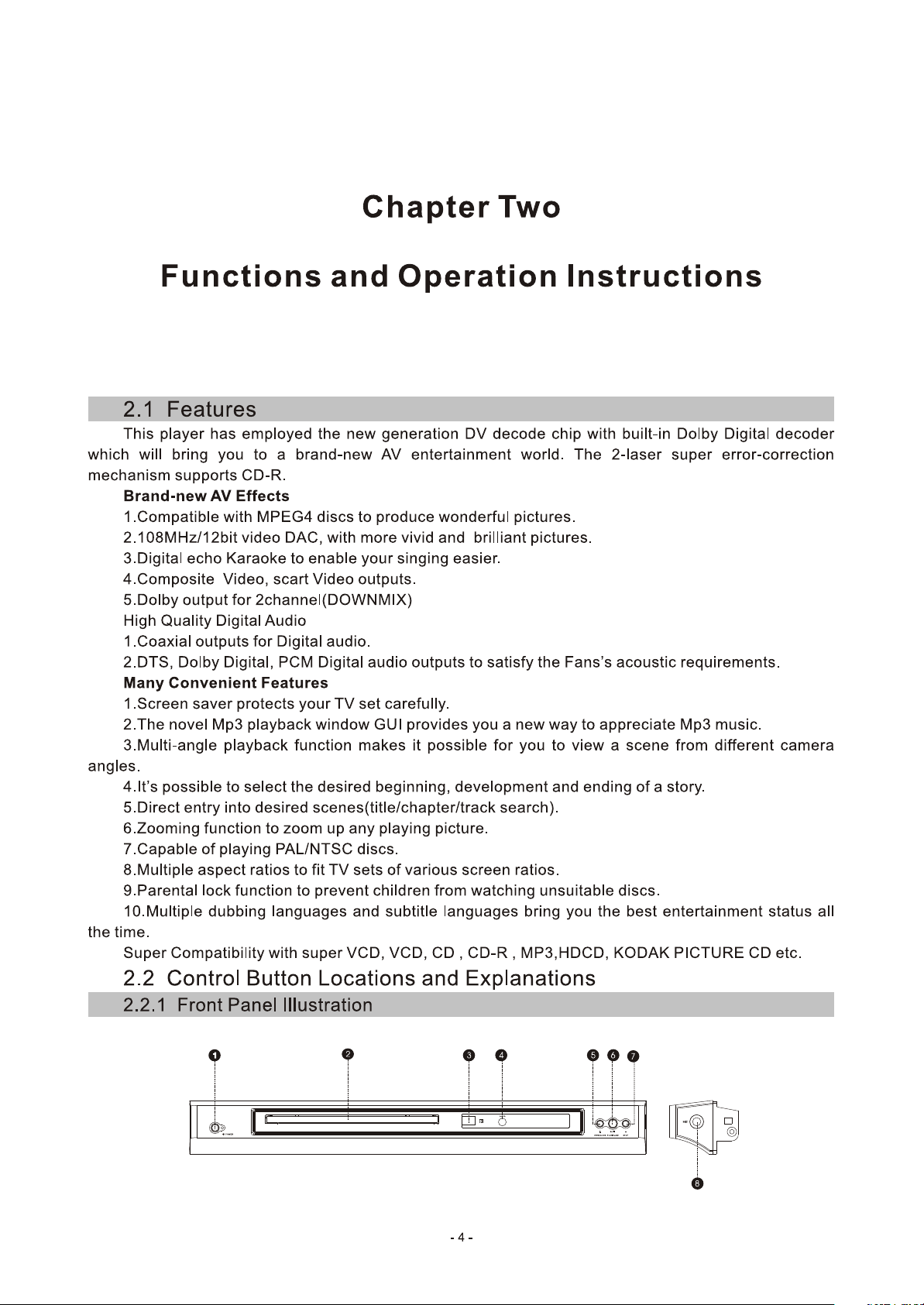
2.1 Features
2.2 Control Button Locations and Explanations
2.2.1 Front Panel Illustration
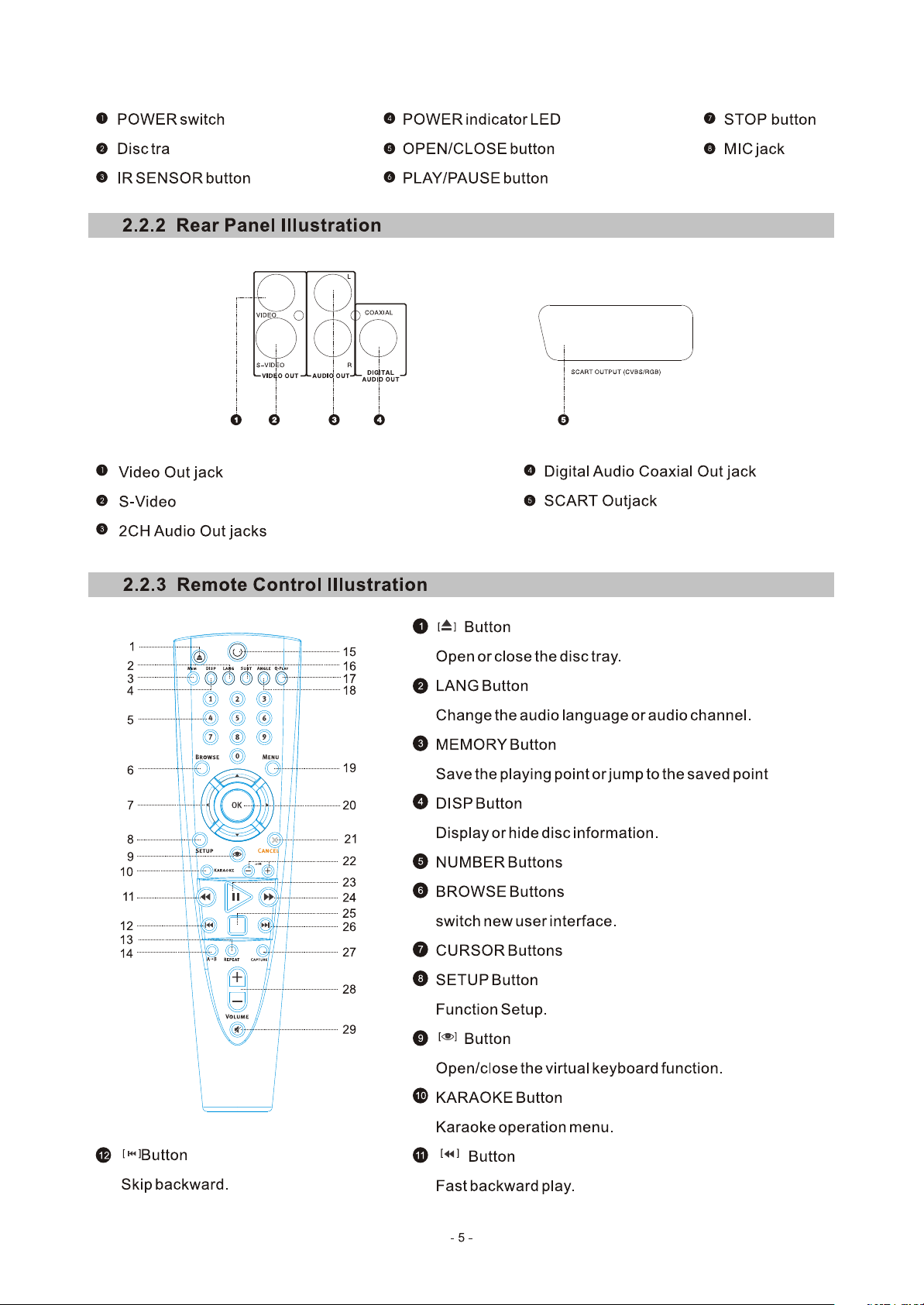
2.2.2 Rear Panel Illustration
2.2.3 Remote Control Illustration
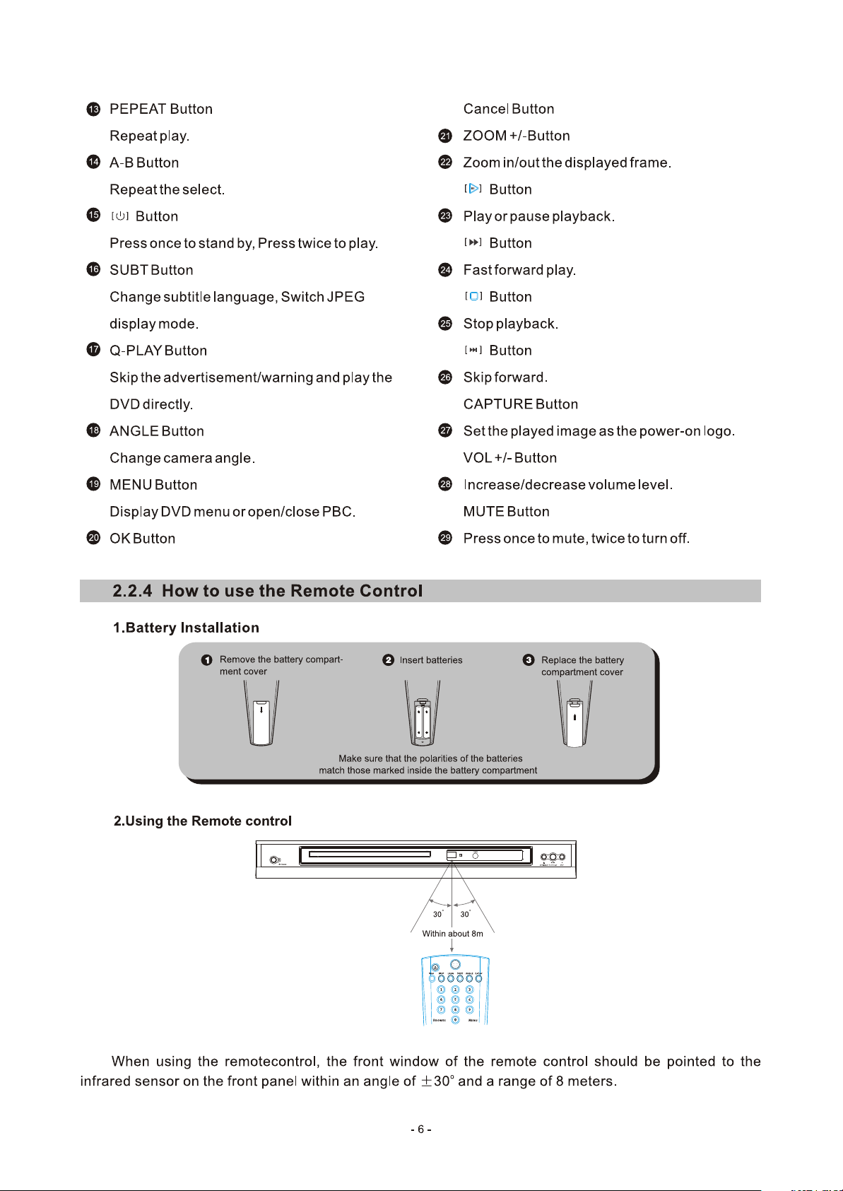
2.2.4 How to use the Remote Control
2.3 Accessories
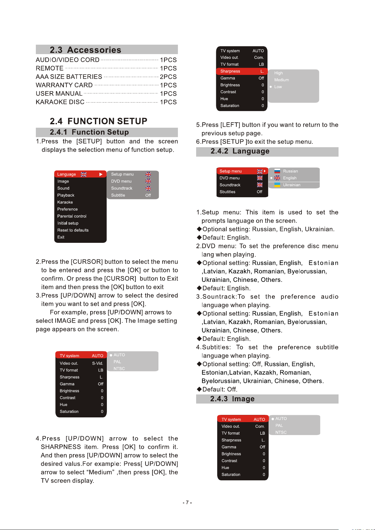
2.4 Function setup
2.4.1 Function setup
2.4.2 language
2.4.3 Image
2.4.4 Sound
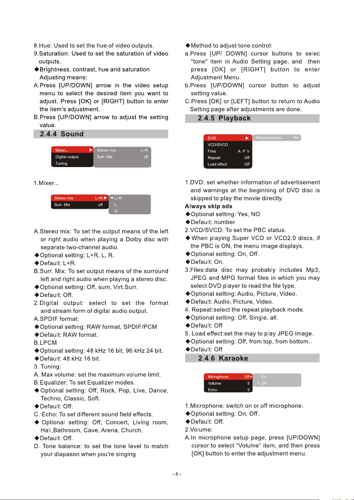
2.4.5 Playback
4
4
4
4
5
5
6
7
7
7
7
7
8
8
Page 3

2.4.6 Karaoke
8
2.4.7 Preference
2.4.8 Parental Control
2.4.9 Initial setup
2.4.10 Rest to defaults
2.4.11 Exit
2.5 Specifications
Chapter Three Principle and Servicing
Section one principle of the player
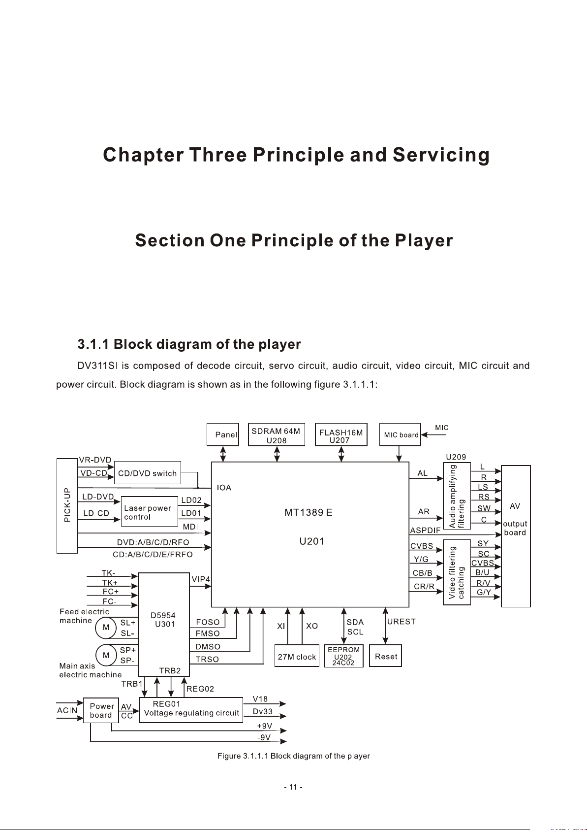
3.1.1 Block diagram of the player
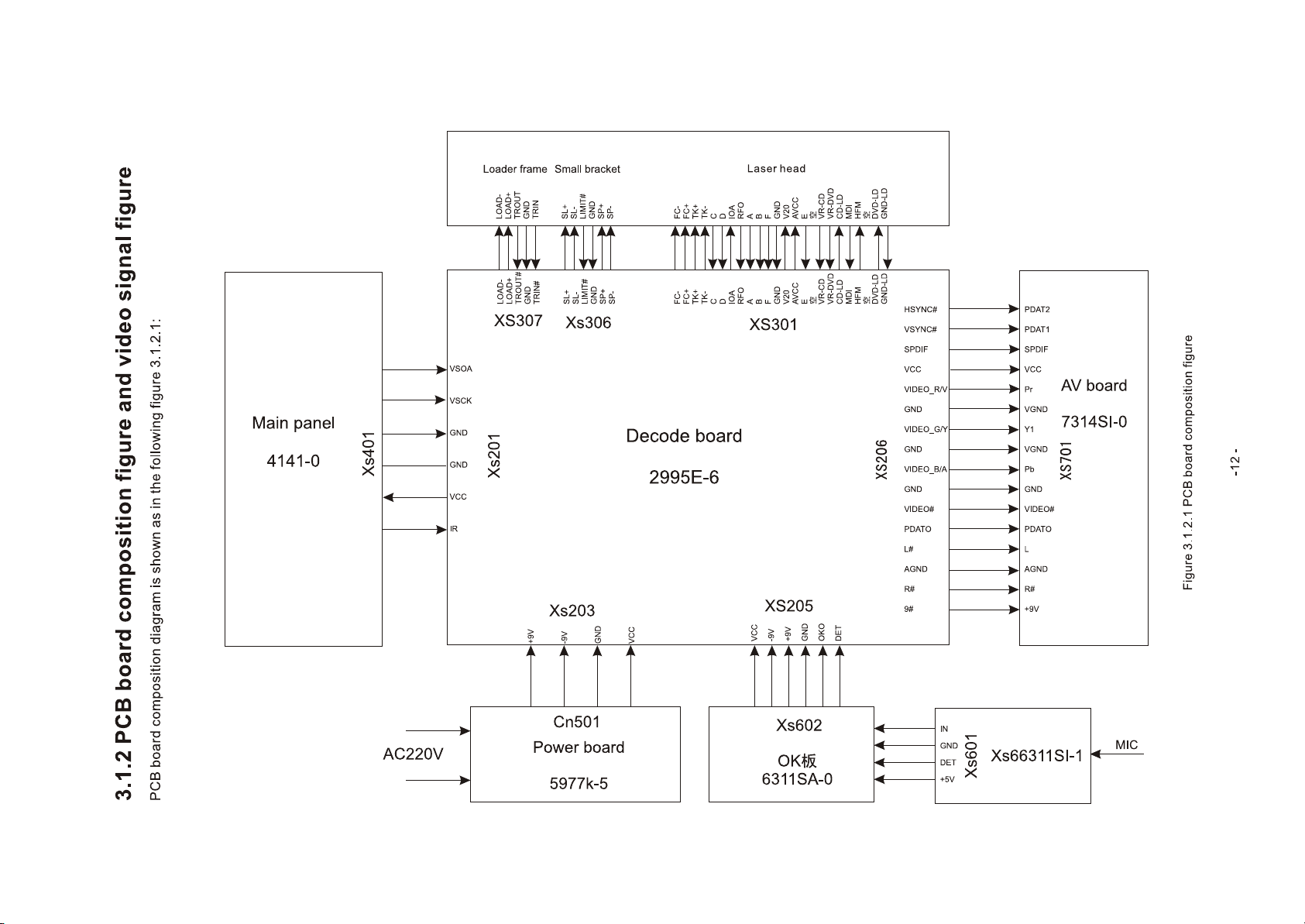
3.1.2 PCB board composition figure and video signal figure
Section Two Unit Circuit Principle
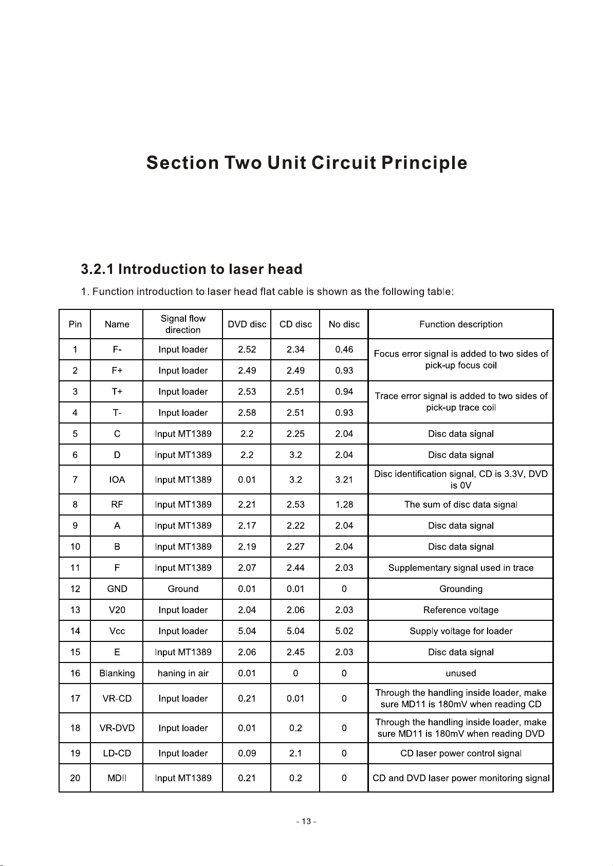
3.2.1 Introduction to laser head
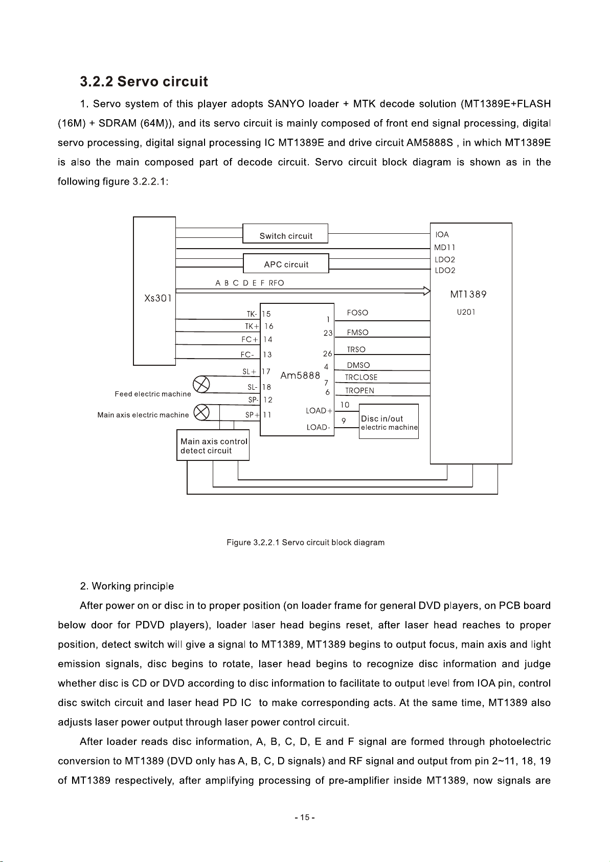
3.2.2 Servo Circuit
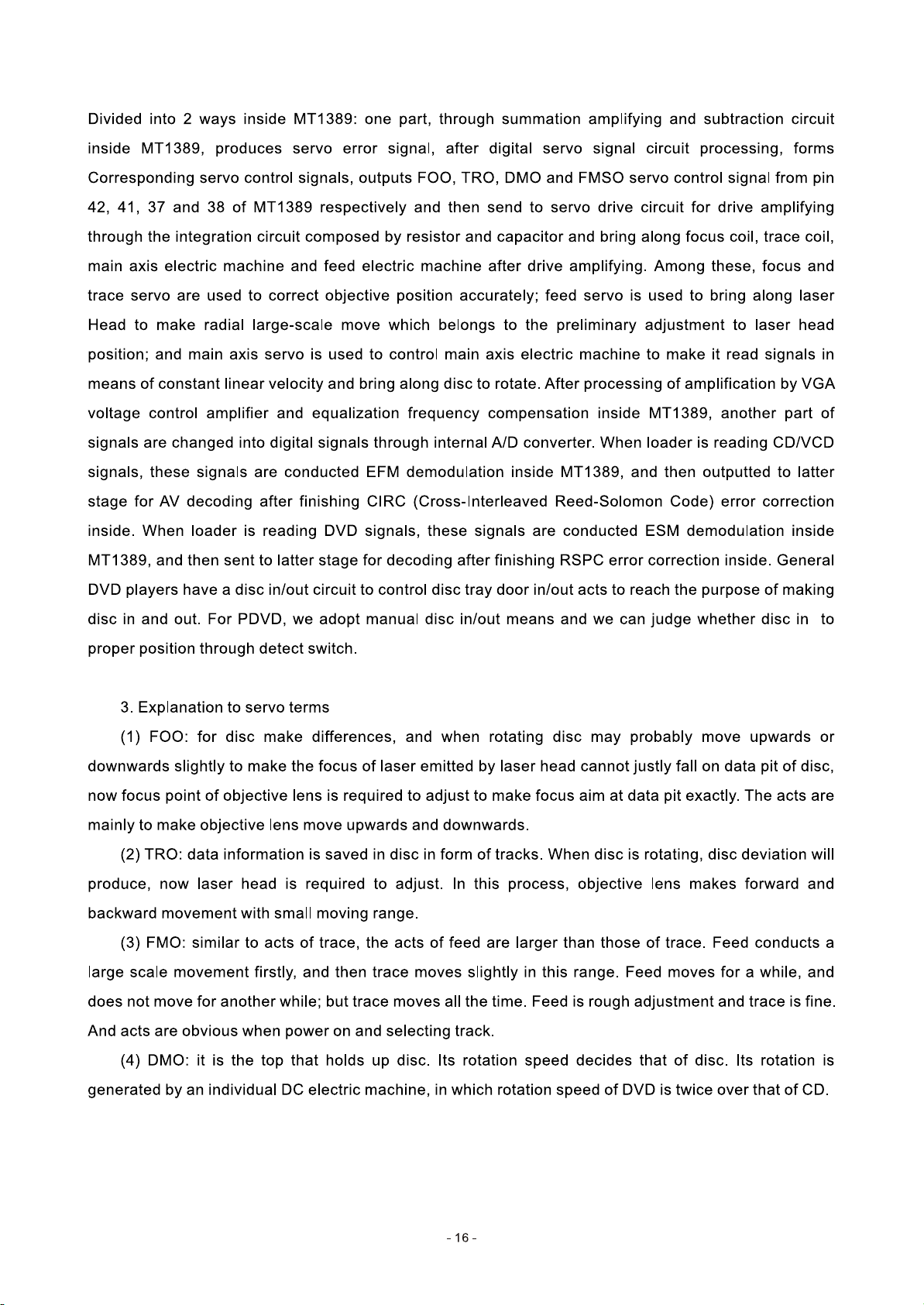
3.2.3 Open/Close drive circuit
9
9
9
9
10
10
11
11
11
12
13
13
15
17
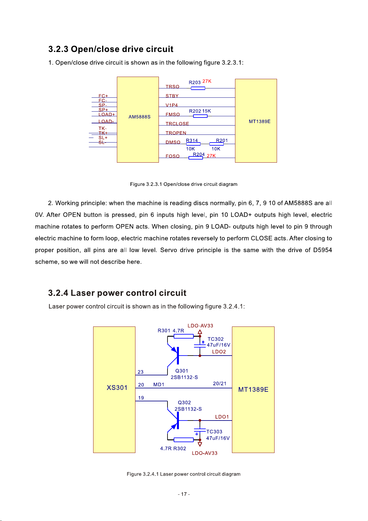
3.2.4 Laser power control circuit
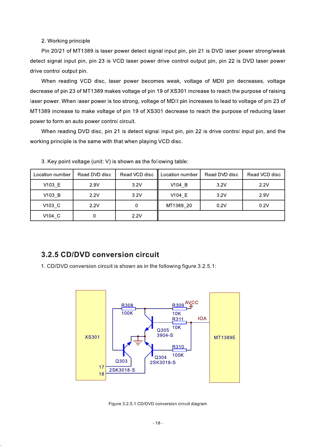
3.2.5 CD/DVD Conversion circuit
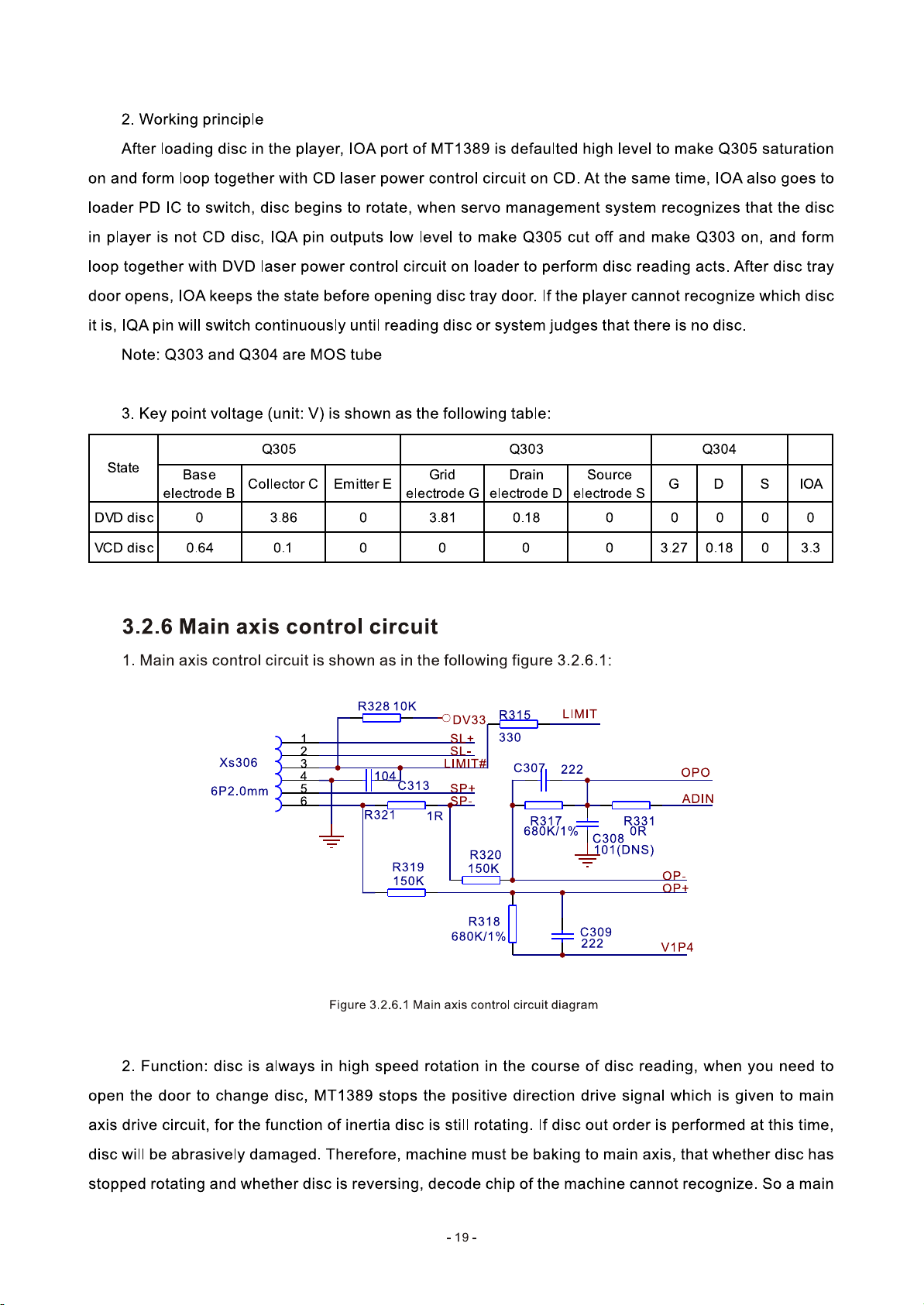
3.2.6 Main axis control circuit
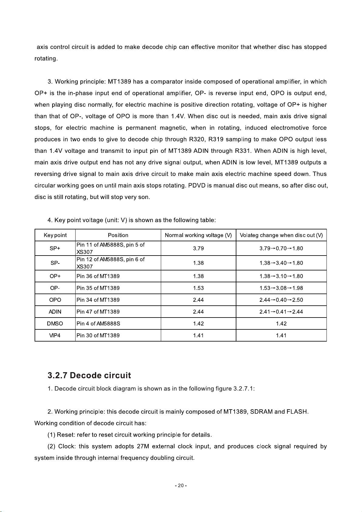
3.2.7 Decode circuit
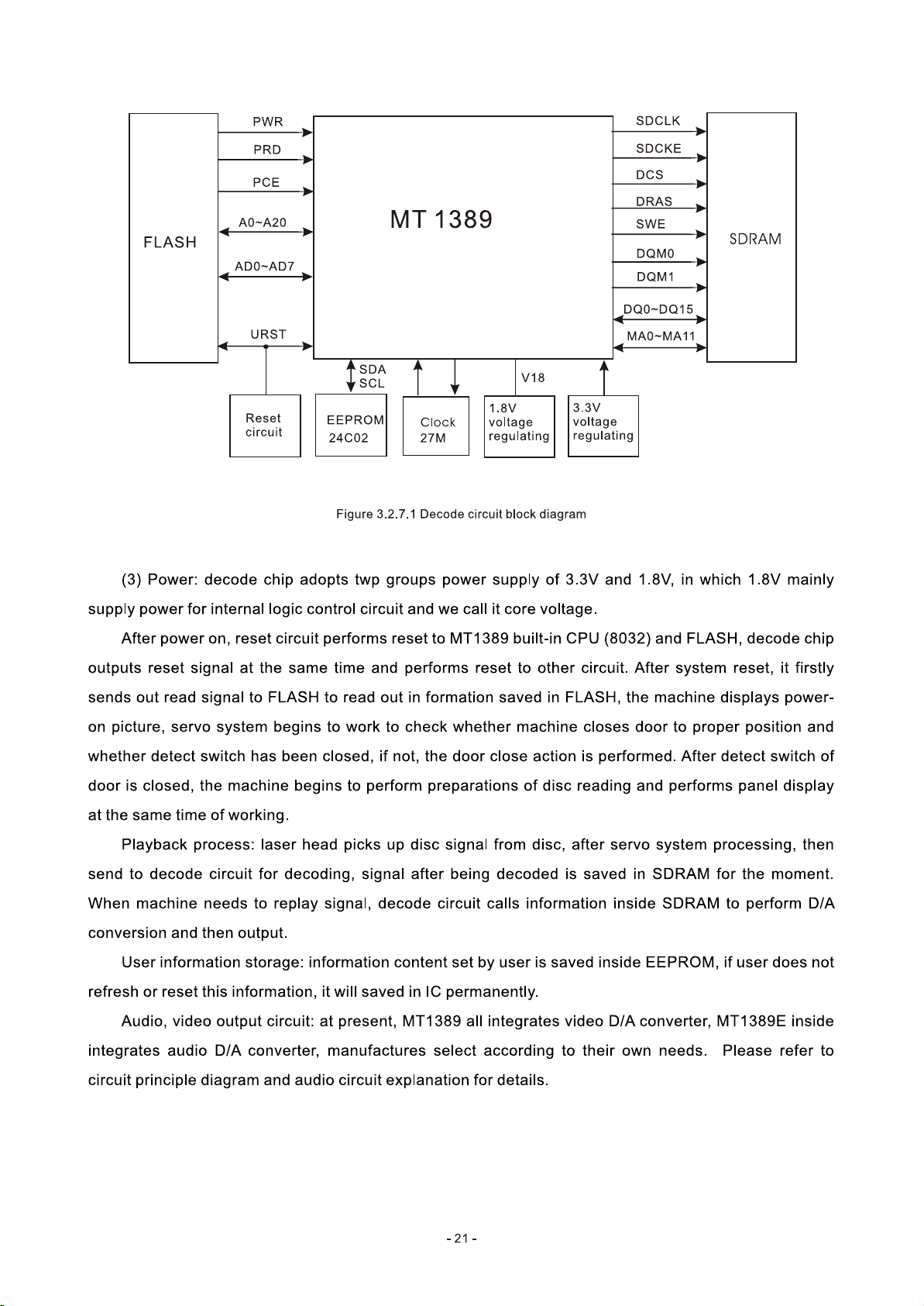
3.2.8 Reset circuit
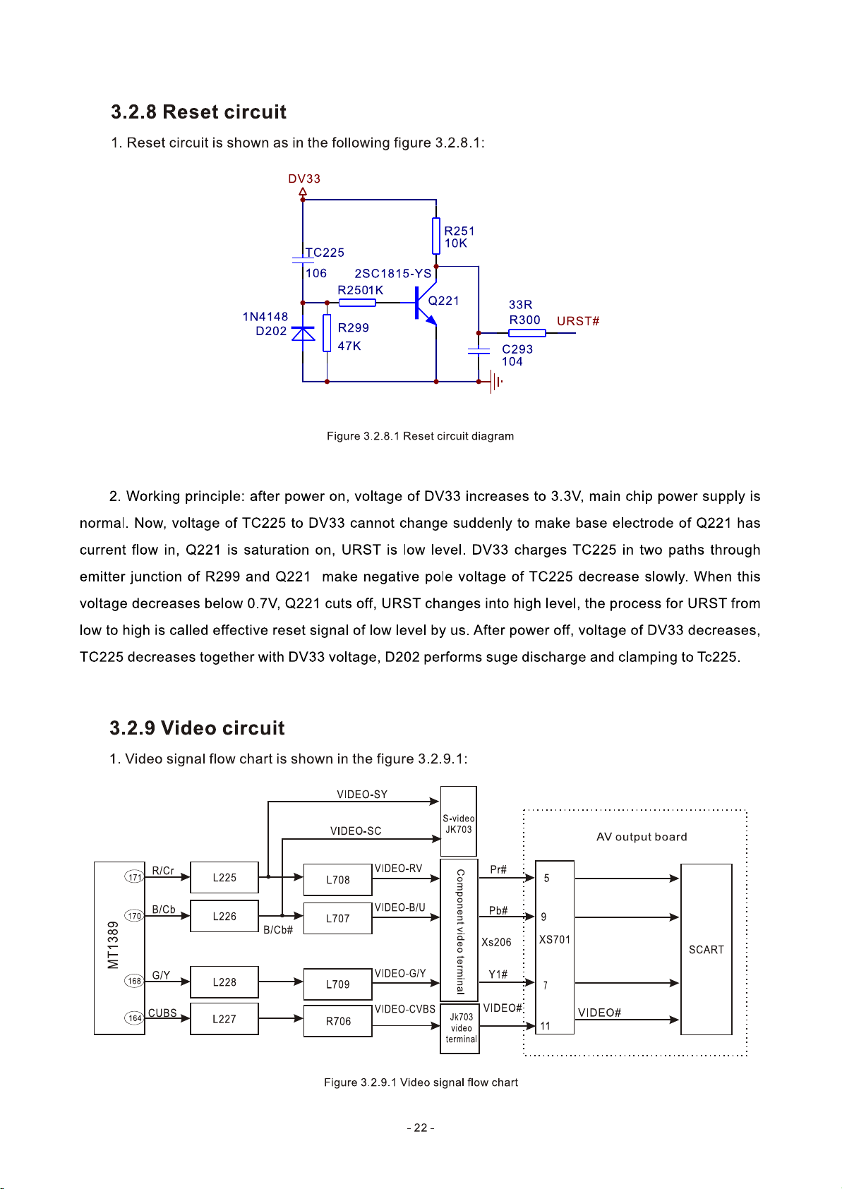
3.2.9 Video circuit
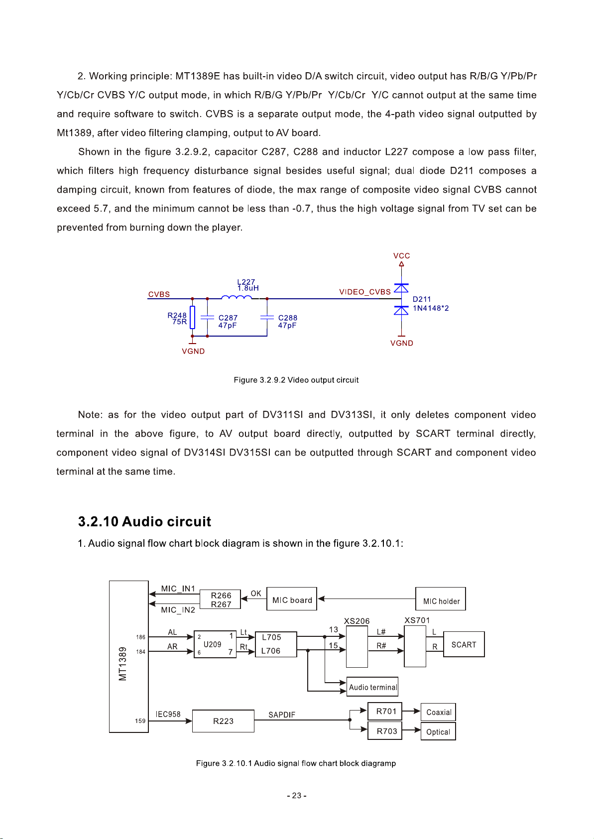
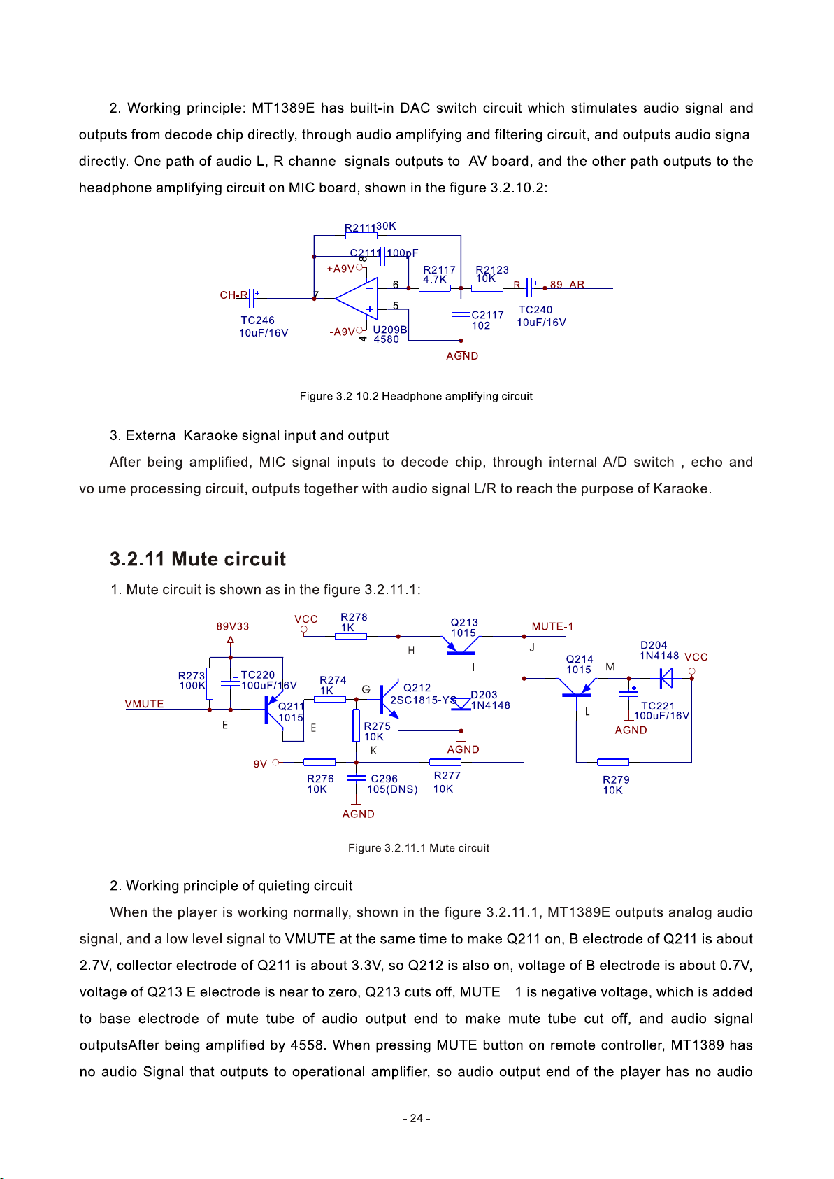
3.2.10 Audio circuit
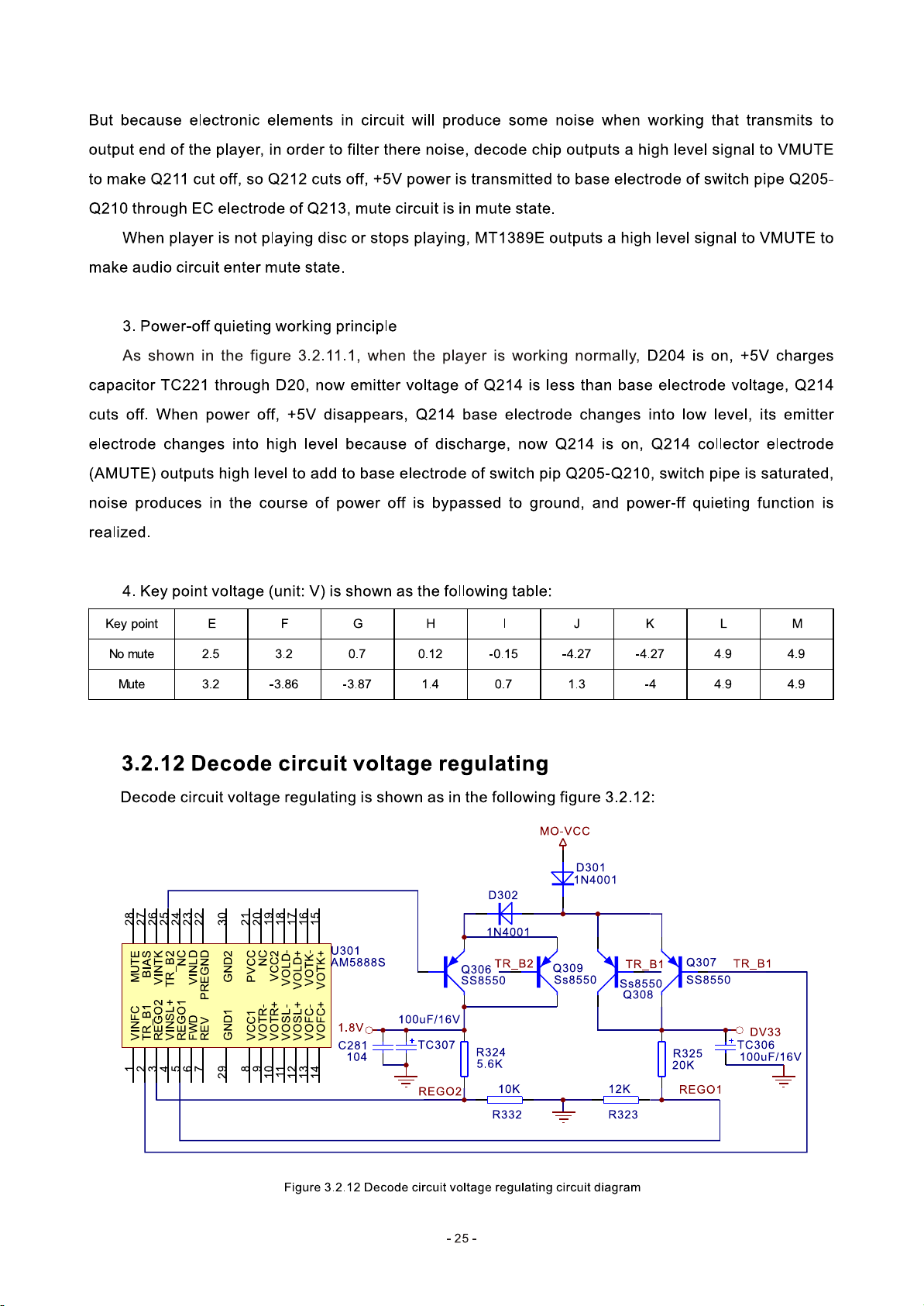
3.2.11 Mute circuit
3.2.12 Decode circuit voltage regulating
3.2.13 Power circuit
3.2.14 Control panel circuit
3.2.15 XIC circuit
3.2.16 AV output board circuit
Section Three Servicing Cases
3.3.1 Servicing instances
17
18
19
20
22
22
23
24
25
26
27
27
28
30
30
3.3.2 Troubleshooting flow chart
Section Four Waveform diagram
Section Five Function Introduction to IC
3.5.1 function introduction to MT1389E
32
45
50
50
Page 4

3.5.2 function introduction to 4558
64
3.5.3 function introduction to AT24C02
3.5.4 function introduction to VIPer22ADIP
3.5.5 function introduction to AM5888S
3.5.6 function introduction to PT6961(4dv315)
3.5.7 Function introduction to SDRAM
3.5.8 Function introduction to FLASH
3.5.9 Function introduction to LM431A
3.5.10 Function introduction to Pc817
Chapter Four Disassembly and Assembly Process
Chapter Cinque PCB board & Circuit diagram
Section One PCB board
Section Two circuit diagram
65
66
67
69
70
72
72
73
74
75
75
82
Chapter six BOM List
DV313SI Service Manual
7.1.1 Features
7.2.1 PCB board block diagram of the player
7.3.1 Control panel circuit
7.4.1 Servicing instances
7.5.1 PCB board
7.5.2 Circuit diagram
DV314SI Service Manual
8.1.1 Features
8.2.1 PCB board block diagram of the player
8.3.1 Control panel circuit
8.4.1 Servicing instances
89
97
97
98
99
99
101
102
103
103
104
105
105
8.5.1 PCB board
8.5.2 Circuit diagram
108
110
Page 5

DV315SI Service Manual
111
9.1.1 Features
9.2.1 PCB board block diagram of the player
9.3.1 Servicing cases
9.3.2 Troubleshooting flow chart
9.4.1 PCB board
9.4.2 Circuit diagram
111
112
113
114
115
116
Page 6

Chapter One About Maintenance
1.1 Safety precautions
1.1.1 Power supply
When maintenance personnel are repairing DVD players, he should pay special attention to the
power board with 220V AC and 330V DC which will cause hurt and damage to persons!
1.1.2 Precautions for antistatic
Movement and friction will both bring static electricity which causes serious damages to integrated
IC. Though static charge is little, when a limited quantity of electric charge is added to large-
scaleintegrated IC, as the capacitance is very small in the meantime, now the integrated IC is very much
easy to be struck through by static electricity or the performance will decrease. Thus static electricity
prevention is of extraordinary importance. The following are several measures to prevent static
electricity:
1. Use a piece of electric conduction metal with the length of about 2 metres to insert into the earth,
and Fetch the lead wire from the top of the surplus metal and connect to the required static electricity
device. The length and depth of the metal embedded under the earth should be determined according to
the wettability of the local soil. For humid places, it may be shorter, and longer and deeper for dry places.
If possible, it can be distributed and layed in terms of “#” shape.
2. On operating table-board, the antistatic table cushion should be covered and grounded.
3. All devices and equipments should be placed on the antistatic table cushion and grounded.
4. Maintenance personnel should wear antistatic wrist ring which should be grounded.
5. Places around the operating position should also be covered with electric conduction cushion or
Painted with antistatic paint.
1.1.3 Precautions for laser head
1. Do not stare at laser head directly, for laser emission will occur when laser head is working, which
will Hurt your eyes!
2. Do not use wiping water or alcohol to clean laser head, and you may use cotton swab.
- 1 -
Page 7

1.1.4 About placement position
1. Never place DVD player in positions with high temperature and humidity.
2. Avoid placing near high magnetic fields, such as loudspeaker or magnet.
3. Positions for placement should be stable and secure.
1.2 Maintenance method
1.2.1 Visualized method
Directly view whether abnormalities of collision, lack of element, joint welding, shedding welding,
rosin joint, copper foil turning up, lead wire disconnection and elements burning up among pins of
elements appear. Check power supply of the machine and then use hands to touch the casing of part of
elements and check whether they are hot to judge the trouble spot. You should pay more attention when
using this method to check in high voltage parts.
1.2.2 Electric resistance method
Set the multimeter in resistance position and test whether the numerical value of resistance of each
point in the circuit has difference from the normal value to judge the trouble spot. But in the circuit the
tested numerical value of resistance is not accurate, and the tested numerical value of integrated IC's
pins can only be used for reference, so the elements should be broken down for test.
1.2.3 Voltage method
Voltage method is relatively convenient, quick and accurate. Set the multimeter in voltage position
and test power supply voltage of the player and voltage of a certain point to judge the trouble spot
according to the tested voltage variation.
1.2.4 Current method
Set the multimeter in current position and test current of the player of a certain point to judge the
trouble spot. But when testing in current method, the multimeter should be series connected in the
circuit, which makes this method too trivial and troublesome, so it is less frequently used in reality.
1.2.5 Cutting method
Cutting method should be combined with electric resistance method and voltage method to use.
This method is mainly used in phenomena of short circuit and current leakage of the circuit. When
cutting the input terminal voltage of a certain level, if voltage of the player rises again, it means that the
trouble lies in this level.
- 2 -
Page 8

1.2.6 Element substitution method
When some elements cannot be judged good or bad, substitution method may de adopted directly.
1.2.7 Comparison method
A same good PC board is usually used to test the correct voltage and waveform. Compared these
data with those tested through fault PC board, the cause of troubles may be found.
Through the above maintenance method, theoretical knowledge and maintenance experience, all
difficulties and troubles will be readily solved.
1.3 Required device for maintenance
Digital oscillograph ( 100MHE)
TV set
SMD rework station
Multimeter
Soldering iron
Pointed-month pincers
Cutting nippers
Forceps
Electric screw driver
Terminals connecting cord
Headphone
Microphone
- 3 -
Page 9
Page 10
Page 11
Page 12
Page 13
Page 14
Page 15
Page 16
Page 17
Page 18
Page 19
Page 20
Page 21
Page 22
Page 23
Page 24
Page 25
Page 26
Page 27
Page 28
Page 29
Page 30
Page 31

Page 32

Page 33

Page 34

Page 35

Page 36

Page 37

Page 38

Page 39

Page 40

Page 41

Page 42

Page 43

Page 44

Page 45

Page 46

Page 47

Page 48

Page 49

Page 50

Page 51

Page 52

Page 53

Page 54

Page 55

Section Five Function Introduction to IC
3.5.1 function introduction to MT1389E
1. DESCRIPTION
MT1389E is a cost-effective DVD system-on-chip (SOC) which incorporates advanced features like
MPEG-4 video decoder, high quality TV encoder and state-of-art de-interlace processing.
Based on MediaTek’s world-leading DVD player SOC architecture, the MT1389E is the 3rd generation of
the DVD player SOC. It integrates the MediaTek 2nd generation front-end analog RF amplifier and the
Servo/MPEG AV decoder.
To enrich the feature of DVD player, the MT1389 equips a simplified MPEG -4 advanced simple profile
(ASP) video decoder to fully support the DivX1 Home Theater profile. It makes the MT1389-based DVD
player be capable of playback MPEG-4 content which become more and more popular.
The progressive scan of the MT1389E utilized advanced motion-adaptive de-interlace algorithm to
achieve the best movie/video playback. It also supports a 3:2 pull down algorithm to give the best film effect.
The 108MHz/12-bit video DAC provides users a whole new viewing experience.
2. Key Features
RF/Servo/MPEG Integration
Embedded 6ch Audio DAC
Embedded 2ch Audio ADC for Karaoke
High Performance Audio Processor
High Performance Progressive Video Processor
Support Nero -Digital
High Quality 108MHz/12-bit, 4 CH TV Encoder
3. General Feature lists
(1)Integration DVD player single chip
High performance analog RF amplifier
Servo controller and data channel processing
MPEG-1/MPEG -2/JPEG video
Dolby AC-3/DTS Decoder
Unified memory architecture
-50 -
Page 56

Versatile video scaling & quality enhancement
OSD & Sub-picture
Built-in clock generator
Built-in high quality TV encoder
Built-in progressive video processor
Audio effect post-processor
Built-in 5.1-ch Audio DAC
Built-in 2-ch Audio ADC for Karaoke
(2)High Performance Analog RF Amplifier
Programmable fc
Dual automatic laser power control
Defect and blank detection
RF level signal generator
(3)Speed Performance on Servo/Channel Decoding
DVD-ROM up to 4XS
CD-ROM up to 24XS
(4)Channel Data Processor
Digital data slicer for small jitter capability
Built-in high performance data PLL for channel data demodulation
EFM/EFM+ data demodulation
Enhanced channel data frame sync protection & DVD-ROM sector sync protection
(5)Servo Control and Spindle Motor Control
Programmable frequency error gain and phase error gain of spindle PLL to control spindle motor on CLV
and CAV mode
Built-in ADCs and DACs for digital servo control
Provide 2 general PWM
Tray control can be PWM output or digital output
(6)Embedded Micro controller
Built-in 8032 micro controller
Built-in internal 373 and 8-bit programmable lower address port
1024-bytes on-chip RAM
Up to 2M bytes FLASH-programming interface
-51 -
Page 57

Supports 5/3.3-Volt. FLASH interface
Supports power -down mode
Supports additional serial port
(7)DVD-ROM/CD-ROM Decoding Logic
High-speed ECC logic capable of correcting one error per each P-codeword or Q-codeword
Automatic sector Mode and Form detection
Automatic sector Header verification
Decoder Error Notification Interrupt that signals various decoder errors
Provide error correction acceleration
(8)Buffer Memory Controller
Supports 16Mb/32Mb/64Mb SDRAM
Supports 16-bit SDRAM data bus
Provides the self-refresh mode SDRAM
Block-based sector addressing
(9)Video Decode
Decodes MPEG1 video an d MPEG2 main level, main profile video (720/480 and 720x576)
Decodes MPEG-4 Advanced Simple Profile
Support DivX 3.11/4.x/5.x Home Theater Profile
Support Nero -Digital
Smooth digest view function with I, P and B picture decoding
Baseline, extended -sequential and progressive JPEG image decoding
Support CD-G titles
(10)Video/OSD/SPU/HLI Processor
Arbitrary ratio vertical/horizontal scaling of video, from 0.25X to 256X
65535/256/16/4/2-color bitmap format OSD,
256/16 color RLC format OSD
Automatic scrolling of OSD image
(11)Audio Effect Processing
Dolby Digital (AC-3)/EX decoding
DTS/DTS-ES decoding
MPEG-1 layer 1/layer 2 audio decoding
MPEG-2 layer1/layer2 2-channel audio
-52 -
Page 58

High Definition Compatible Digital (HDCD)
Windows Media Audio (WMA)
Dolby ProLogic II
Concurrent multi-channel and downmix out
IEC 60958/61937 output
PCM / bit stream / mute mode
Custom IEC latency up to 2 frames
Pink noise and white noise generator
Karaoke functions
Microphone echo
Microphone tone control
Vocal mute/vocal assistant
Key shift up to +/- 8 keys
Chorus/Flanger/Harmony/Reverb
Channel equalizer
3D surround processing include virtual surround and speaker separation
(12)TV Encoder
Four 108MHz/12bit DACs
Support NTSC, PAL-BDGHINM, PAL-60
Support 525p, 625p progressive TV format
Automatically turn off unconnected channels
Support PC monitor (VGA)
Support Macrovision 7.1 L1, Macrovision 525P and 625P
CGMS-A/WSS
Closed Caption
(13)Progressive Scan Video
Automatic detect film or video source
3:2 pull down source detection
Advanced Motion adaptive de-interlace
Minimum external memory requirement
(14)Outline
216-pin LQFP package
3.3/1.8-Volt. Dual operating voltages
-53 -
Page 59

4. PIN DESCRIPTION
PIN
191
192
212
213
214
215
216
1 AGND Ground Analog ground
2 DVDA Analog input AC couple input path A
3 DVDB Analog input AC couple input path B
4 DVDC Analog input AC couple input path C
5 DVDD Analog input AC couple input path D
Main Alt Type Description
RF interface (26)
RFGND18 Ground Analog ground
RFVDD Power Analog power 1.8V
OSP Analog output RF Offset cancellation capacitor connecting
OSN Analog output RF Offset cancellation capacitor connecting
RFGC Analog output RF AGC loop capacitor connecting for DVD-ROM
Current reference input. It generates reference current for RF
IREF Analog input
path. Connect an external 15K resistor to this pin and AVSS
AVDD3 Power Analog power 3.3V
6 DVDRFIP Analog input AC coupled DVD RF signal input RFIP
7 DVDRFIN Analog input AC coupled DVD RF signal input RFIN
8 MA Analog input DC coupled main beam RF signal input A
9 MB Analog input DC coupled main beam RF signal input B
10 MC Analog input DC coupled main beam RF signal input C
11 MD Analog input DC coupled main beam RF signal input D
12 SA Analog input DC coupled sub-beam RF signal output A
13 SB Analog input DC coupled sub-beam RF signal output B
14 SC Analog input DC coupled sub-beam RF signal output C
15 SD Analog input DC coupled sub-beam RF signal output D
PIN
16 CDFON Analog input CD focusing error negative input
17 CDFOP Analog input CD focusing error positive input
18 TNI Analog input 3 beam satellite PD signal negative input
19 TPI Analog input 3 beam satellite PD signal positive input
Main Alt Type Description
ALPC (4)
20 MIDI1 Analog input Laser power monitor input
21 MIDI2 Analog input Laser power monitor input
-54 -
Page 60

22 LDO2 Analog output Laser driver output
23 LDO1 Analog output Laser driver output
Reference voltage (3)
28 V2REFO Analog output Reference voltage 2.8V
29 V20 Analog output Reference voltage 2.0V
30 VREFO Analog output Reference voltage 1.4V
Analog monitor output (7)
24 SVDD3 Power Analog power 3.3V
25 CSO RFOP Analog output
1) Central servo
2) Positive main beam summing output
1) RFRP low pass, or
26 RFLVL RFON Analog output
2) Negative main beam summing output
27 SGND Ground Analog ground
31 FEO Analog output Focus error monitor output
32 TEO Analog output Tracking error monitor output
33 TEZISLV Analog output TE slicing Level
Analog Servo Interface (8)
204
205
206
207
208
209
ADCVDD3 Power Analog 3.3V power for ADC
ADCVSS Ground Analog ground for ADC
RFVDD3 Power Analog power
RFRPDC Analog output RF ripple detect output
RFRPAC Analog input RF ripple detect input (through AC-coupling)
HRFZC Analog input High frequency RF fipple zero crossing
210
211
PIN
195
196
197
198
199
200
201
CRTPLP Analog output Defect level filter capacitor connecting
RFGND Ground Analog power
RF Data PLL Interface (9)
Main Alt Type Description
JITFO Analog output Output terminal of RF jitter meter
JITFN Analog Input Input terminal of RF jitter meter
PLLVSS Ground Ground pin for data PLL and related analog circuitry
IDACEXLP Analog output Data PLL DAC Low -pass filter
PLLVDD3 Power Power pin for data PLL and related analog circuitry
LPFON Analog Output Negative output of loop filter amplifier
LPFIP Analog input Positive input terminal of loop filter amplifier
-55 -
Page 61

202
LPFIN Analog input Negative input terminal of loop filter amplifier
203
LPFOP Analog output Positive output of loop filter amplifier
Motor and Actuator Driver Interface (10)
34 OP_OUT Analog output Op amp output
35 OP_INN Analog input Op amp negative input
36 OP_INP Analog input Op amp positive input
37 DMO Analog output Disk motor control output. PWM output
38 FMO Analog output Feed motor control. PWM output
TROPENPW
39
Analog output Tray PWM output/Tray open output
M
3) 1st General PWM output
40 PWMOUT1 ADIN0 Analog output
4) AD input 0
Tracking servo output. PDM output of tracking servo
41 TRO Analog output
compensator
Focus servo output. PDM output of focus servo
42 FOO Analog output
compensator
43
48
84
132
146
74
120
PIN
60
87
108
137
LVTTL3.3 Input,
1) Monitor hall sensor input
FG
ADIN1
Schmitt input, pull up,
2) AD input 1
(Digital pin)
GPIO
with analog input path
3) GPIO
for ADIN1
General Power/Ground (11)
DVDD18 Power 1.8V power pin for internal digital circuitry
DVSS Ground 1.8V ground pin for internal digital circuitry
Main Alt Type Description
DVDD3 Power 3.3V power pin for internal digital circuitry
149
DVSS Ground 3.3V ground pin for internal digital circuitry
Micro Controller and Flash Interface (48)
54 HIGHA0 InOut 4~16mA, Microcontroller address 8
-56 -
Page 62

SRPU
66 HIGHA1
65 HIGHA2
64 HIGHA3
63 HIGHA4
62 HIGHA5
61 HIGHA6
59 HIGHA7
81 AD7
InOut 4~16mA,
Microcontroller address 9
SRPU
InOut 4~16mA,
Microcontroller address 10
SRPU
InOut 4~16mA,
Microcontroller address 11
SRPU
InOut 4~16mA,
Microcontroller address 12
SRPU
InOut 4~16mA,
Microcontroller address 13
SRPU
InOut 4~16mA,
Microcontroller address 14
SRPU
InOut 4~16mA,
Microcontroller address 15
SRPU
InOut 4~16mA,
Microcontroller address/data 7
SRPU
78 AD6
Microcontroller address/data 6
SRPU
InOut 4~16mA,
InOut 4~16mA,
77 AD5
Microcontroller address/data 5
SRPU
InOut 4~16mA,
76 AD4
Microcontroller address/data 4
SRPU
InOut 4~16mA,
75 AD3
Microcontroller address/data 3
SRPU
InOut 4~16mA,
73 AD2
Microcontroller address/data 2
SRPU
72 AD1 InOut 4~16mA, Microcontroller address/data 1
PIN
Main Alt Type Description
InOut 4~16mA,
Microcontroller address/data 0
71 AD0
SRPU
InOut 4~16mA,
83 IOA 0
Microcontroller address
SRPU
69 IOA 1
Microcontroller address 1/ IO
SRPU
47 IOA 2 InOut 4~16mA, Microcontroller address 2/ IO
InOut 4~16mA,
-57 -
Page 63

SRPU
49 IOA 3
50 IOA 4
51 IOA 5
52 IOA 6
53 IOA 7
58 A16
82 A17
55 A18
InOut 4~16mA,
SRPU
InOut 4~16mA,
SRPU
InOut 4~16mA,
SRPU
InOut 4~16mA,
SRPU
InOut 4~16mA,
SRPU
InOut 4~16mA,
SRPU
InOut 4~16mA,
SRPU
InOut 4~16mA,
SRPD,SMT
Microcontroller address 3/ IO
Microcontroller address 4/ IO
Microcontroller address 5/ IO
Microcontroller address 6/ IO
Microcontroller address 7/ IO
Flash address 16
Flash address 17
Flash address 18 /IO
56 A19
YUV0
67 A20
YUV7
79 A21
GPIO
80 ALE
PIN
Main Alt Type Description
70 IOOE#
57 IOER#
InOut 4~16mA,
SRPD,SMT
Flash address 19 /IO
5) Flash address 20 /IO
InOut 4~16mA,
6) While External Flash size <= 1MB:
SRPD,SMT
I) Alternate digital video YUV output 0
7) Flash address 21 /IO
InOut 4~16mA,
SRPD,SMT
8) While External Flash size <= 2MB:
I) Digital video YUV output 7
II) GPIO
InOut 4~16mA,
Microcontroller address latch enable
SRPD,SMT
InOut 4~16mA,
Flash output enable, active low / IO
SRPD,SMT
InOut 4~16mA,
Flash write enable, active low / IO
SRPD,SMT
InOut 4~16mA,
Flash chip select, active low / IO
68 IOCS#
SRPD,SMT
85 UWR# InOut 4~16mA, Microcontroller write strobe, active low
-58 -
Page 64

SRPD,SMT
86 URD#
88 UP1_2
89 UP1_3
91 UP1_4
92 UP1_5
93 UP1_6 SCL
94 UP1_7 SDA
95 UP3_0 RXD
InOut 4mA,
SRPD,SMT
InOut 4~16mA,
SRPD,SMT
InOut 4mA,
SRPD,SMT
InOut 4mA,
SRPD,SMT
InOut 4mA,
SRPD,SMT
InOut 4mA,
SRPD,SMT
InOut 4mA,
SRPD,SMT
InOut 4mA,
SRPD,SMT
Microcontroller read strobe, active low
Microcontroller port 1-2
Microcontroller port 1-3
Microcontroller port 1-4
Microcontroller port 1-5
9) Microcontroller port 1-6
10) I2C clock pin
11) Microcontroller port 1-7
12) I2C data pin
13) Microcontroller port 3-0
14) 8032 RS232 RxD
96 UP3_1 TXD
RXD
97 UP3_4
SCL
RXD
98 UP3_5
SDA
102
103
PIN
IR Input SMT IR control signal input
INT0#
Main Alt Type Description
YUV1
153
ALRCK
GPO
InOut 4mA,
SRPD,SMT
InOut 4mA,
SRPD,SMT
InOut 4~16mA,
SRPD,SMT
InOut 4~16mA,
SRPD,SMT
InOut 4mA,
PD,SMT
15) Microcontroller port 3-1
16) 8032 RS232 TxD
17) Microcontroller port 3-4
18) Hardwired RD232 RxD
19) I2C clock pin
20) Microcontroller port 3-5
21) Hardwired RD232 TxD
22) I2C data pin
Microcontroller external interrupt 0, active low
1) Audio left/right channel clock
2) Trap value in power-on reset:
I) 1: use external 373
II) 0: use internal 373
3) While internal audio DAC used:
I) Digital video YUV output 1
II) GPO
-59 -
Page 65

4) Audio bit clock
151
152
154
ABCK
ACLK
ASDATA0
YUV0
GPIO
YUV0
GPIO
YUV2
GPO
InOut 4mA,
SMT
InOut 4mA,
SMT
InOut 4mA,
PD,SMT
5) While internal audio DAC used:
I) Digital video YUV output 0
II) GPIO
6) Audio DAC master clock
7) While internal audio DAC used:
I) Alternate digital video YUV output 0
II) GPIO
8) Audio serial data 0 (Front-Left/Front-Right)
9) Trap value in power-on reset:
I) 1: manufactory test mode
II) 0: normal operation
10) While internal audio DAC used:
I) Digital video YUV output 2
II) GPO
11) Audio serial data 1 (Left-Surround/Right-Surround)
12) Trap value in power-on reset:
155
156
PIN
157
ASDATA1
YUV4
GPO
InOut 4mA,
II) 0: normal operation
PD,SMT
13) While only 2 channels output:
I) Digital video YUV output 4
II) GPO
14) Audio serial data 2 (Center/LFE)
15) Trap value in power-on reset:
I) 1: manufactory test mode
YUV5
InOut 4mA,
I) 1: manufactory test mode
ASDATA2
GPO
PD,SMT
II) 0: normal operation
16) While only 2 channels output:
I) Digital video YUV output 5 II) GPO
Main Alt Type Description
17) Audio serial data 3 (Center-back/
Center-left-back/Center-right-back, in 6.1 or 7.1 mode)
ASDATA3
YUV6
GPIO
InOut 4mA,
18) While only 2 channels output:
PD,SMT
I) Digital video YUV output 6
II) GPIO
158
MC_DATA
YUV0
INT2#
InOut 2mA,
19) Microphone serial input
20) While not support Microphone:
-60 -
Page 66

Output
I) Microcontroller external interrupt 2
II) Digital video YUV output 0
III) GPIO
159
172
173
174
175
176
177
178
179
180
181
182
183
SPDIF
4~16mA,
S/PDIF output
SR: ON/OFF
AADVSS Ground Ground pin for 2ch audio ADC circuitry
AKIN2 Analog Audio ADC input 2
ADVCM Analog 2ch audio ADC reference voltage
AKIN1 Analog Audio ADC input 1
AADVDD Power 3.3V power pin for 2ch audio ADC circuitry
APLLVDD3 Power 3.3V Power pin for audio clock circuitry
APLLCAP Analog InOut APLL external capacitance connection
APLLVSS Ground Ground pin for audio clock circuitry
ADACVSS2 Ground Ground pin for audio DAC circuitry
ADACVSS1 Ground Ground pin for audio DAC circuitry
21) Audio DAC sub-woofer channel output
ARF GPIO Output
22) While internal audio DAC not used: GPIO
23) Audio DAC right Surround channel output
ARS GPIO Output
24) While internal audio DAC not used: GPIO
184
185
186
PIN
187
188
189
25) Audio DAC right channel output
26) While internal audio DAC not used:
AR GPIO Output
a. SDATA1
b. GPIO
AVCM Analog Audio DAC reference voltage
27) Audio DAC left channel output 28) While internal audio
AL Output
DAC not used: a. SDATA2 b. GPIO
Main Alt Type Description
29) Audio DAC left Surround channel output
30) While internal audio DAC not used:
ALS Output
c. SDATA0
d. GPIO
31) Audio DAC center channel output
ALF Output
32) While internal audio DAC not used: GPIO
ADACVDD1 Power 3.3V power pin for audio DAC circuitry
-61 -
Page 67

190
ADACVDD2 Power 3.3V power pin for audio DAC circuitry
Video Interface (12)
160
161
162
163
164
165
166
167
168
169
170
171
DACVDDC Power 3.3V power pin for video DAC circuitry
VREF Analog Bandgap reference voltage
FS Analog Full scale adjustment
DACVSSC Ground Ground pin for video DAC circuitry
InOut 4mA,
CVBS
Analog composite output
SR
DACVDDB Power 3.3V power pin for video DAC circuitry
DACVSSB Ground Ground pin for video DAC circuitry
DACVDDA Power 3.3V power pin for video DAC circuitry
InOut 4mA,
Green, Y, SY, or CVBS
Y/G
SR
DACVSSA Ground Ground pin for video DAC circuitry
InOut 4mA,
B/CB/PB
Blue, CB/PB, or SC
SR
InOut 4mA,
R/CR/PR
Red, CR/PR, CVBS, or SY
SR
101
PRST#
PD,SMT
InOut
100
193
194
ICE InOut PD,SMT Microcontroller ICE mode enable
XTALO Output 27MHz crystal output
XTALI Input 27MHz crystal input
VSYN
InOut 4mA,
44 GPIO0
PIN
YUV1
Main Alt Type Description
SR,SMT
HSYN
InOut 4mA,
45 GPIO1
INT4#
SR,SMT
YUV2
46 GPIO2 SPMCLK InOut 2mA
MISC (12)
Power on reset input, active low
33) General purpose IO 0
34) Vertical sync for video input
35) Digital video YUV output 1
36) General purpose IO 1
37) Horizontal sync for video input
38) Microcontroller external interrupt 4
39) Digital video YUV output 2
40) General purpose IO 2
41) Audio S/PDIF SPMCLK input
147
GPIO3 INT1# InOut 2mA 42) General purpose IO 3
-62 -
Page 68

SPDATA 43) Microcontroller external interrupt 1
44) Audio S/PDIF SPDATA input
148
GPIO4 SPLRCK InOut 2mA
INT3#
150
GPIO5
SPBCK
90 GPIO6 YUVCLK
99 GPIO7 YUV3
145
144
143
142
RA4 InOut DRAM address 4
RA5 InOut DRAM address 5
RA6 InOut DRAM address 6
RA7 InOut DRA M address 7
45) General purpose IO 4
46) Audio S/PDIF SPLRCK input
47) General purpose IO 5
InOut 2mA
48) Microcontroller external interrupt 3
49) Audio S/PDIF SPBCK input
InOut 4mA,
50) General purpose IO 6
SR,SMT
51) Digital video clock output
InOut 4mA,
SR,SMT
52) General purpose IO 7
53) Digital video YUV output 3
Dram Interface (38) (Sorted by position)
141
140
139
138
136
135
134
133
131
130
PIN
129
128
127
126
RA8 InOu DRAM address 8
RA9 InOut DRAM address 9
RA11 InOut Pull-Down DRAM address bit 11
CKE Output DRAM clock enable
RCLK InOut Dram clock
RA3 InOut DRAM address 3
RA2 InOut DRAM address 2
RA1 InOut DRAM address 1
RA0 InOut DRAM address 0
RA10 InOut DRAM address 10
Main Alt Type Description
BA1 InOut DRAM bank address 1
BA0 InOut DRAM bank address 0
RCS# Output DRAM chip select, active low
RAS# Output DRAM row address strobe, active low
125
124
CAS# Output DRAM column address strobe, active low
RWE# Output DRAM Write enable, active low
-63 -
Page 69

123
DQM1 InOut Data mask 1
122
121
119
118
117
116
115
114
113
112
111
110
109
107
106
RD8 InOut DRAM data 8
RD9 InOut DRAM data 9
RD10 InOut DRAM data 10
RD11 InOut DRAM data 11
RD12 InOut DRAM data 12
RD13 InOut DRAM data 13
RD14 InOut DRAM data 14
RD15 InOut DRAM data 15
RD0 InOut DRAM data 0
RD1 InOut DRAM data 1
RD2 InOut DRAM data 2
RD3 InOut DRAM data 3
RD4 InOut DRAM data 4
RD5 InOut DRAM data 5
RD6 InOut DRAM data 6
105
104
RD7 InOut DRAM data 7
DQM0 InOut Data mask 0
3.5.2 function introduction to 4558
1. Description
The RC4558 and RM4558 devices are dual general-purpose operational amplifiers with each half
electrically similar to the A741 except that offset null capability is not provided.?
The high common -mode input voltage range and the absence of latch-up make these amplifiers ideal for
voltage-follower applications. The devices are short -circuit protected and the internal frequency compensation
ensures stability without external components.
The RC4558 is characterized for operation from 0 C to 70 C, and the RM4558 is characterized for ? ?
operation over the full military temperature range of –55 C to 125 C.
2. FEATURES
◆ Continuous-Short-Circuit Protection
◆ Wide Common-Mode and Differential
◆ Voltage Ranges
◆ No Frequency Compensation Required
-64 -
Page 70

◆ Low Power Consumption
◆ No Latch-Up
◆ Unity-Gain Bandwidth . . . 3 MHz Typ
◆ Gain and Phase Match Between Amplifiers
◆ Low Noise . . . 8 nV?Hz Typ at 1 kHz
◆ Designed To Be Interchangeable With
◆ Raytheon RC4558 and RM4558 Devices
3. PIN CONFIGURATION
PIN No Symbol I/O
1 1OUT O
2 1IN– I
3 1IN+ I
PIN No. Symbol I/O
PIN No. Symbol I/O
4 VCC– I
5 2IN+ I
6 2IN– I
7 2OUT O
8 VCC+ I
3.5.3 function introduction to AT24C02
1. Description
Description
Output 1
Inverting Input Pin 1
Non-Inverting Input Pin 1
Description
Description
Negative Power Supply
Non-Inverting Input Pin 2
Inverting Input Pin 2
Output 2
Positive Power Supply
The AT24C02 provides 2048 bits of serial electrically erasable and programmable read-only memory
(EEPROM) organized as 256 words of 8 bits each. The device is optimized for use in many industrial and
commercial applications where low-power and low-voltage operation are essential. The AT24C02 is available
in space-saving 8-lead PDIP,
8-lead MAP, 8 lead TSSOP and 8-ball dBGA2 packages and is accessed via a 2-wire serial interface. In
addition, the entire family is available in 2.7V (2.7V to 5.5V) and 1.8V (1.8V to 5.5V) versions.
2. Features
◆ Low-voltage and Standard-voltage Operation
– 2.7 (VCC = 2.7V to 5.5V)
– 1.8 (VCC = 1.8V to 5.5V)
◆ Internally Organized, 256 x 8 (2K),
-65 -
Page 71

◆ 2-wire Serial Interface
◆ Schmitt Trigger, Filtered Inputs for Noise Suppression
◆ Bi-directional Data Transfer Prot ocol
◆ 100 kHz (1.8V) and 400 kHz (2.5V, 2.7V, 5V) Compatibility
◆ Write Protect Pin for Hardware Data Protection
◆ 8-byte Page (1K, 2K), Write Modes
◆ Partial Page Writes are Allowed
◆ Self-timed Write Cycle (5 ms max)
◆ High-reliability
◆ – Endurance: 1 Million Write Cycles
◆ – Data Retention: 100 Years
◆ Automotive Grade, Extended Temperature and Lead-Free Devices Available
◆ 8-lead PDIP, 8-lead JEDEC SOIC, 8-lead MAP, 5-lead SOT23,
◆ 8-lead TSSOP and 8-ball dBGA2™ Packages
3. PIN DESCRIPTION
PIN No. Symbol I/O Description
1 A0 I To Ground
2 A1 I To Ground
3 A2 I To Ground
4 VSS I To Ground
5 SDA I/O Serial Data input
6 SCL I/O Serial SCL input
7 TEST I/O Test port
8 VDD I Positive Power Supply
3.5.4 function introduction to VIPer22ADIP
1. DESCRIPTION
The VIPer22A combines a dedicated current mode PWM controller with a high voltage Power MOSFET
on the same silicon chip. Typical applications cover off line power supplies for battery charger adapters,
standby power supplies for TV or monitors, auxiliary supplies for motor control, etc. The internal control circuit
offers the following benefits:
– Large input voltage range on the VDD pin accommodates changes in auxiliary supply voltage. This
feature is well adapted to battery charger adapter configurations.
– Automatic burst mode in low load condition.
-66 -
Page 72

– Overvoltage protection in hiccup mode.
2. FEATURES
◆ FIXED 60 KHZ SWITCHING FREQUENCY
◆ 9V TO 38V WIDE RANGE VDD VOLTAGE
◆ CURRENT MODE CONTROL
◆ AUXILIARY UNDERVOLTAGE LOCKOUT WITH HYSTERESIS
◆ HIGH VOLTAGE START UP CURRENT SOURCE
◆ OVERTEMPERATURE, OVERCURRENT AND OVERVOLTAGE PROTECTION WITH
AUTORESTART
3. PIN DESCRIPTION
PIN Symbol I/O Description
1 SOURCE O Power MOSFET source and circuit ground reference.
2 SOURCE O Power MOSFET source and circuit ground reference.
3 FB I Feedback input.
4 VDD I Power supply of the control circuits.
5 DRAIN I Power MOSFET drain.
6 DRAIN I Power MOSFET drain.
7 DRAIN I Power MOSFET drain.
8 DRAIN I Power MOSFET drain.
3.5.5 function introduction to AM5888S
1. Description
The AM5888S is a five-channel BTL driver IC for driving the motors and actuators such as used in DVD
player and consists of two independent precision voltage regulators with adjustable range from 1.5V to 4 V. It
supports a variety of applications. Also, Pb free package is selectable (Please refer to Marking Identification).
2. Fetures
1) Two channels are voltage-type BTL drivers for actuators of tracking and focus. Two channels are
voltage-type BTL driver for sled and spindle motors. It is also built-in one channel bi-direction DC motor driver
for tray.
2) Wide dynamic range [9.0V (typ.) when Vcc1= Vcc2= 12V, at RL= 20¦¸ load].
3) Separating power of Vcc1 and Vcc2 is to improve power efficiency by a low supply voltage for tracking,
focus, and spindle.
-67 -
Page 73

4) Level shift circuit built-in.
5) Thermal shut down circuit built-in.
6) Mute mode built-in.
7) Dual actuator drivers:
A general purpose input OP provides differential input for signal addition. The output structure is two
power OPAMPS in bridge configuration.
8) Sled motor driver:A general purpose input OP provides differential input for signal addition. The output
structure is one power OPAMP in bridge configuration.
9) Spindle driver:Single input linear BTL driver. The output structure are two power OPAMPS in bridge
configuration.
10) Tray in-out driver:The DC motor driver supports forward/reverse control for tray motor.
11) 2 Built -in regulator controllers: Adjustable range 1.5V ~ 4V
3. PIN DESCRIPTION
PIN Symbol I/O Description
1 VINFC I Input for focus drive
2 TRB_1 O Connect to external transistor base
3 REGO2 O Regulator voltage output, connect to external transistor collector
4 VINSL I Input for the sled driver
5 REGO1 O Regulator voltage output, connect to external transistor collector
6 FWD I Tray driver forward input
7 REV I Tray driver reverse input
8 VCC1 I Vcc for pre-drive block and power block of sled and tray
9 VOTR- O Tray driver output (-)
10 VOTR+ O Tray driver output (+)
11 VOSL+ O Sled driver output (+)
12 VOSL- O Sled driver output (-)
13 VOFC- O Focus driver output (-)
14 VOFC+ O Focus driver output (+)
15 VOTK+ O Tracking driver output (+)
16 VOTK- O Tracking driver output (-)
17 VOLD+ O Spindle driver output (+)
18 VOLD- O Spindle driver output (-)
19 VCC2 I Vcc for power block of spindle, tracking and focus
20 NC No Connection
-68 -
Page 74

21 VCTL I Speed control input of tray driver
22 GND I Ground
23 VINLD I Input for spindle driver
24 NC No Connection
25 TRB_2 O Connect to external transistor base
26 VINTK I Input for tracking driver
27 BIAS I Input for reference voltage
28 MUTE I Input for mute control
3.5.6 function introduction to PT6961(4dv315)
1. DESCRIPTION
PT6961 is an LED Controller driven on a 1/7 to 1/8 duty factor. Eleven segment output lines, six grid
output lines, 1 segment/grid output lines, one display memory, control circuit, key scan circuit are all
incorporated into a single chip to build a highly reliable peripheral device for a single chip microcomputer.
Serial data is fed to PT6961 via a four-line serial interface. Housed in a 32-pin SO Package, PT6961 pin
assignments and application circuit are optimized for easy PCB Layout and cost saving advantages.
2. FEATURES
◆ CMOS Technology
◆ Low Power Consumption
◆ Multiple Display Modes (12 segment, 6 Grid to 11 segment, 7 Grid)
◆ Key Scanning (10 x 3 Matrix)
◆ 8-Step Dimming Circuitry
◆ Serial Interface for Clock, Data Input, Data Output, Strobe Pins
◆ Available in 32-pin, SOP Package
3. PIN DESCRIPTION
PIN Symbol I/O Description
1 OSC I Oscillator Input P in
2 DOUT O Data output
3 DIN I Data input
4 CLK I Clock input
5 STB I Serial interface strobe
6 K1 I Key data input
-69 -
Page 75

7 K2 I Key data input
8 K3 I Key data input
9 VDD I Power supply
10 SG1/KS1 O Segment output
11 SG2/KS2 O Segment output
12 SG3/KS3 O Segment output
13 NC
14 SG4/KS4 O Segment output
15 SG5/KS5 O Segment output
16 SG6/KS6 O Segment output
17 SG7/KS7 O Segment output
18 SG8/KS8 O Segment output
19 SG9/KS9 O Segment output
20 SG10/KS10 O Segment output
21 SG11 O Segment output
22 SG12/GR7 O Segment output
23 GR6 O Grid output
24 GR5 O Grid output
25 VDD I Power input
26 GND I Ground
27 GR4 O Grid output
28 GR3 O Grid output
29 GND I Ground
30 GR2 O Grid output
31 GR1 O Grid output
32 GND I Ground
3.5.7 Function introduction to SDRAM
64M 16-bit memorizer SDRAM with the player and the working clock frequency is 166/143MHZ. The
function of 16SDRAM in DVD players is to memorizer the program of AML3298 taken out from FLASH and
information of image and sound taken out from disc to form buffer, add the stability of information output and
add ant i-shaking effect of player. Pin function introduction is shown as the following table:
-70 -
Page 76

Pin Name
1 VDD 3.3V power supply 28 VSS Ground
2 DQ0 Data bus I/O 29 MA4 Address bus I
Function Signal flow Pin Name Function Signal flow
3 VDDQ
4 DQ1 Data bus I/O 31 MA6 Address bus I
5 DQ2 Data bus I/O 32 MA7 Address bus I
6 VSSQ
7 DQ3 Data bus I/O 34 MA9 Address bus I
8 DQ4 Data bus I/O 35 MA11 Address bus I
9 VDDQ
10
DQ5 Data bus I/O 37 CKE Clock enable signal I
11 DQ6 Data bus I/O 38 CLK System clock input I
12 VSSQ
13
DQ7 Data bus I/O 40 NC Blank
14 VDD 3.3V power supply 41 VSS Ground
15 LDQM
3.3V power supply I/O 30 MA5 Address bus I
Ground 33 MA8 Address bus I
3.3V power supply 36 NC Blank
Data input/output
Ground 39 UDQM
screen-shielded signal
Data input/output screen-shielded
I 42 DQ8 Data bus I/O
signal
I
16
17 CAS Line address gating signal I 44 DQ9 Data bus I/O
18 RAS Row address gating signal I 45 DQ10
19
20 SD -BS0 Segmanr address 0 gating signal
21 SD -BS1 Segmanr address 1 gating signal
22 MA10
23 MA0 Address bus I 50 DQ13
24 MA1 Address bus I 51 DQ14
25 MA2 Address bus I 52 VSSQ
26 MA3 Address bus I 53 DQ15
27 VDD 3.3V power supply 54 VSS Ground
WE Write control signal I 43 VDDQ
CS Chip selection signal I 46 VSSQ
I 47 DQ11 Data bus I/O
I 48 DQ12
Address bus I 49 VDDQ
3.3V power supply
Data bus I/O
Ground
Data bus I/O
3.3V power supply
Data bus I/O
Data bus I/O
Ground
Data bus I/O
-71 -
Page 77

3.5.8 Function introduction to FLASH
R
FLASH (U214) is a 16Mbit FLASH memorizer, and the damage of U214 may cause troubles, such as
power not on, no disc reading and power on picture mosaic. Pin function is shown as the following table:
Pin Name Function Voltage (when no disc) Data direction
1-9、16-25、48
11 WE Write enable signal, low level is effective 3.23V I
12 RESET Reset, low level is effective 3.23V I
10、13、14
15 RY/BY Ready/system busy 3.23V O
26 CE Chip enable, low level effective 0V I
27、46
28 OE Output enable signal , low level is effective 0V I
29-3、6、38 -44
37 VCC 5V power supply +5V
45 DQ15/A-1
47 BYTE
AO-A19 20 bit address bus I
NC Blank pin
VSS Ground
DQ0-DQ14
Take word extend mode as data line, and bit extend
Select 8-bit or 16-bit output mode. High level is 16-bit
output and low level is 8-bit output
15 bit data bus O
I/O
mode as address line
I
3.5.9 Function introduction to LM431A
U503 (LM431A) is a 2.5V comparator, shown as the figure 3.5.9.1. Compared the inputted voltage of R end
with 2.5V, when voltage of R end is more than 2.5V, KA end is on and photoelectric coupler starts to send out
photocurrent; when voltage of R end is less than 2.5V, KA end is cutoff and photoelectric coupler does not send
out photocurrent. CPU+3.3V in power board circuit must be kept in 3.3V, for the function of comparator. No
matter more than or less than 3.3V, through on and off status of comparator, it will control the on state of the
output end of photoelectric coupler LM431A to adjust the output space occupation ratio of switch module to
control the output voltage of transformer and masthead the power.
K
A
Figure 3.5.9.1 LM431A outside drawing
-72 -
Page 78

3.5.10 Function introduction to Pc817
U502 (2501) is a photoelectric coupler, shown as the figure 3.5.10.1. The right side is a light emitting diode,
which sends out light of different intensity according to the strength of voltage inputted from the right side,
generates photocurrent of different intensity on the left side according to light of different intensity, and outputs
from position D. The higher of the voltage inputted from the right side, the stronger of the light emitted from
light emitting diode and the larger of the photocurrent produced from position D. The lower of the voltage
inputted from the right side of photoelectric coupler, the weaker of the light emitted from light emitting diode
and the weaker of the current outputted from position D.
Figure 3.5.10.1 2501 outside drawing
-73 -
Page 79

Page 80

Chapter Cinque
PCB board & Circuit diagram
Section One PCB board
5.1.1 Surface layer of AV OUT Board
L713
7314SI-0 LEI
DVD 2006/03/21
R#
L#
AGND
XS702
L714
V701
R706
PDAT2
PDAT1
- 75 -
L701
L702 L703 L704
PR#
R708
AGND
V703
R709
R#
+10V
JP701
V702
Y1#
PDAT0
PB#
L#
VIEDO
XS706
Page 81

5.1.2 Bottom layer of AV OUT Board
C724
R711
R712
C728
C723
ZD704
ZD703
R704
R710
ZD702
ZD701
R715
R714
C726
R705
C716
C727
C725
D701
D702
R713
R716
- 76 -
Page 82

5.1.3 Surface layer of DECODE&SERVO Board
- 77 -
Page 83

5.1.4 Bottom layer of DECODE&SERVO Board
- 78 -
Page 84

5.1.5 MIC Board
XS602
R619
C619
+5V
-9V
+9V
GND
OKA
DET
R632
R633
R620
Q601
+
TC616 C602
TC613
+
TC615 C601
R626
C607
R613
U601
R612
C605
1
+5V
DET
GND
IN
R609
R607
JP601
TC603
6311SA-0 TANG
DVD 2006/03/08
TC605
XS601
- 79 -
Page 85

5.1.6 KEY SCAN Board
U403
XS401
C405
TC407
VO G
R415
+
JP401
JP402
IR
VCC
DST
GND
DCK
LED402
DAT
LED
R418
R417
R416
R402
LED403
H=5.5MM
R406
R407
Q401
LED401
R401
4141-0 LEI
2004.05.07
D401
K402
K403K401
- 80 -
Page 86

5.1.7 POWER Board
G502
G501
GND
+3.3V
GND
+5V
GND
-9V
+9V
R501
L501
BCN503
CAUTION:
BC501
T1.6AL 250V
F502
FOR CONTINUED
PROTECTION AGAINST
RISK OF FIRE
ONLY WITH SAME TYPE
T1.6AL 250V FUSE
F501
REPLACE
F501
AC 220V IN
BCN501
V
S
JP502
TC510
CN502
JP501
CN501
+9V
-9V
GND
+5V
R517
D513
R509
C508
D509
R507
TC513
C510
R508
R506
R511
TC506
TC504
+
+
ZD502
TC505
L507
L505
TC512
D510
TC503
JP503
6
7
8
9
10
U503
C515
JP504
D511
D508
BC503
T501
U502
5241-0
2006/3/18
R512
D506
R505
+
TC502
C504
R503
D504
C506
D501
D502
D503
BCN502
TC501
U501
5
L503
4
C503
3
2
1
D505
C502
- 81 -
Page 87

5.2.1 MPEG&SERVO Board 1
Section Two circuit diagram
MIC_DET
MIC_IN1
MIC_IN2
Q211
1015
102
102
C298
C299
C328
101
R278
+9V
1K
R274
1K
R276
10K
102
89V33
C297
DET
OK
GND
+9V
-9V
VCC
TC220
100uF/16V
-9V
R2123
10K
C2117
222
R2124
10K
C2118
222
R271
36K(NC)
R272
36K(NC)
30K
R2111
C2111 150pF
R2135
Q205
2SC1815-YS
Q206
2SC1815-YS
1K
R2136
1K
R2137
1K
R2138
1K
Rt
- 82 -
R2147
100K
AGND
R2148
100K
Lt
MUTE-1
CH-R
CH-L
TC246
10uF/1206
TC247
10uF/1206
R109 1
7
1
R109 1
+A9V
-A9V
R2112
C2112 150pF
+A9V
-A9V
R2117
4.7K
6
5
U209B
4 8
4580
30K
U209A
4 8
4580
AGND
R2118
4.7K
2
3
AGND
+9V
C2130
104
AGND
-9V
C2133
104
AGND
OKA
R
AGND
L
TC222
100uF/16V
TC223
100uF/16V
C2129
102(DNS)
R205
0R
TC240
10uF/16V
TC241
10uF/16V
OK
89_AR
89_AL
VMUTE
R273
100K
1
2
3
4
5
6
AGND
XS205
2.0mm
10K
C296
105(DNS)
R265 330R
R266 0R
R267 0R
Q212
2SC1815-YS
R277
10K
OK OKA#
Q213
1015
D203
1N4148
AGND
C292
1U
MUTE-1
DET
OKA#
OKA#
Q214
1015
89V33
AGND
ZD203
3V/0.5W
ZD204
2.7V/0.5W
AGNDR275
R279
10K
D204
1N4148
TC221
100uF/16V
VCC
Page 88

VREF
SPDIF
ALRCK
ACLK
ABCK
GPIO5
DVSS
GPIO4
GPIO3
RA11
DVDD3
RCLK
RA10
RCS#
RAS#
CAS#
RWE#
DQM1
DVSS
RD10
RD11
RD12
RD13
RD14
RD15
C276
33pF
FS
RA4
RA5
RA6
RA7
RA8
RA9
CKE
RA3
RA2
RA1
RA0
BA1
BA0
RD8
RD9
RD0
RD1
RD2
RD3
RD4
DACVDD3 89V33
L206
FBSMT
TC212
10uF/16V
4.7K
R270
ASDAT2
R207 1K
ALRCK
R206 560R
FS
C216 104
VREF
R223
75R
89V33 V18
FS
VREF
DACVDD3
IEC958
AMDAT
ASDAT3
ASDAT2
ASDAT1
ASDAT0
ALRCK
ACLK
ABCK
TROUT
TRIN
LIMIT
-12V
162
161
160
159
158
157
156
155
154
153
152
151
150
149
148
147
146
145
144
143
142
141
140
139
138
137
136
135
134
133
132
131
130
129
128
127
126
125
124
123
122
121
120
119
118
117
116
115
114
113
112
111
110
109
C242
104
SPDIFIEC958
MA4
MA5
MA6
MA7
MA8
MA9
MA11
DCKE
DCLK
MA3
MA2
MA1
MA0
MA10
BA1
BA0
CS#
RAS#
CAS#
WE#
DQM1
DQ8
DQ9
DQ10
DQ11
DQ12
DQ13
DQ14
DQ15
DQ0
DQ1
DQ2
DQ3
DQ4
5.2.2 MPEG&SERVO Board 2
C243
104
VMUTE
AVCC
2SK3018-S
R329
10K
R340 330R
R377 330R
C311
103
Q305
3904-S
Q304
4.7uH
FBSMT
4.7uH
FBSMT
1R
LIMIT#
R309
10K
R311
10K
R310
100K
U301
15
VOTK+
16
VOTK-
17
VOLD+
18
VOLD-
19
VCC2
20
NC
21
PVCC
30
GND2
22
PREGND
23
VINLD
24
NC
25
TR_B2
26
VINTK
27
BIAS
MUTE28VINFC
AM5888S
DV33
SL+
SL-
SP+
SP-
R320
150K
R318
680K/1%
TROUT
TRIN
AVCC
R315
330
C301
104
MDI
E
V20
F
B
A
RFO
IOA
D
C
TKTK+
FC+
FC-
C307 222
R317
680K/1%
IOA
220uF/16V
VOFC+
VOFC-
VOSL+
VOSL-
VOTR+
VOTR-
VCC1
GND1
REV
FWD
REGO1
VINSL+
REGO2
TR_B1
TC301
LIMIT
89V33
C309
222
C308
2SB1132-S
14
13
12
11
10
9
8
29
7
6
5
4
3
2
1
101(DNS)
L316
FBSMT
R301
4.7R
Q301
Q302
2SB1132-S
R302
4.7R
FCSPSP+
LOAD+
LOADMO-VCC
GND
TRCLOSE
TROPEN
REGO1
REGO2
FOSO
R331
0R
LDO-AV33
LDO-AV33
C237
222
OPO
ADIN
OPOP+
V1P4
C281
104
C318
104
TC302
47uF/16V
LDO2
LDO1
TC303
47uF/16V
RFVDD3
LDO-AV33
C238
103
C316
104
R314
10K
100uF/16V
C319
104
C239
104
TC307
C246
104
PLLVDD3
AADVDD3
C236
104
L203
FBSMT
MO-VCC
C317
104
V18 RFV18
C229
104
C247
C248
104
104
89V33
TC304
100uF/16V
DMSO
D302
1N4001
Q306
SS8550
R324
5.1K
10K
R332
220uF/6.3V
330uH
L315
FBSMT
L201
FBSMT
R303
10R
TC207
100uF/16V
L202
4.7uH
TC208
C249
104
L204
MO-VCC
C230
104
89V33
89V33
89V33
C250
104
C240
103
VCC
FMSO
TRSO
FOSO
V1P4
C210
153
D301
1N4001
Q309
SS8550(DNS)
1.8V
TC209
220uF/6.3V
ADACVDD3
C207
104
C208
104
C209
104
C212
C211
104
SS8550(DNS)
Q308
12K
R323
TC210
220uF/6.3V
C2154
1uF
C2156
1uF
C2158
1uF
R201
R202
R203
R204
C213
331
TR_B1TR_B2
APLLVDD3 89V33
TC205
10uF/16V
89_SW
89_AR
89_ARS
184
182
183
ARS
ARF(SW)
AR/SDATA1
VSCK
C241
104
181
180
179
ADACVSS2
ADACVSS1
VSDA
VSTB
IOA
L205
4.7uH
C218
152
APLLVDD3
178
177
APLLVSS
APLLCAP
APLLVDD
SCL
SDA
C217
MIC_IN1
ADVCM
AADVDD3
175
174
176
AKIN1
ADVCM
AADVDD
UP3_196UP3_4
95
97
MIC_DET
RXD
FS0
104
MIC_IN2
173
172
AKIN2
UP3_598GPIO799ICE
TRCLOSE
TXD
TC204
10uF/16V
B/Cb
R/Cr
171
170
B/Cb/SC
AADVSS
R/Cr/CVBS/SY
PRST#
100
101IR102
ICE
URST#
C219 391
V18
L219
C231
FBSMT
104
C201 105
C
C202 105
B
C203 105
A
C204 105
D
C205 105(DNS)
RFO
C206
101
C2155
1uF
C2157
1uF
C2159
C214
1uF
104
10KDMSO
15K
27K
27K
331
Q307
TR_B1TR_B2
SS8550
DV331.8V
TC306
R325
100uF/16V
20K
REGO1REGO2
C
B
A
D
SUBA
SUBB
SUBC
SUBD
E
F
MDI
LDO2
LDO1
RFOP
RFON
V2P8
V20
V1P4
FEO
TEO
TEZISLV
OPO
OPOP+
DMO
FMO
TROPEN
V1P4_IN
TRO
FOO
ADIN
VSYNC#
HSYNC#
STBY
A2
A3
A4
A5
A6
A7
A8
C232
104
RFVDD3
V18
C233
104
C260
104
R211
15K
C234
104
10
11
12
13
14
15
16
17
18
19
20
21
22
23
24
25
26
27
28
29
30
31
32
33
34
35
36
37
38
39
40
41
42
43
44
45
46
47
48
49
50
51
52
53
54
C228
RFVDD3
1
AGND
2
DVDA
3
DVDB
4
DVDC
5
DVDD
6
DVDRFIP
7
DVDRFIN
8
MA
9
MB
MC
MD
SA
SB
SC
SD
CDFON
CDFOP
TNI
TPI
MDI1
MDI2
LDO2
LDO1
SVDD3
CSO/RFOP
RFLVL/RFON
SGND
V2REFO
V20
VREFO
FEO
TEO
TEZISLV
OP_OUT
OP_INN
OP_INP
DMO
FMO
TROPENPWM
PWMOUT1/ADIN0
TRO
FOO
FG/ADIN1
GPIO0/VSYNC#
GPIO1/HSYNC#
GPIO2
IOA2
DVDD18
IOA3
IOA4
IOA5
IOA6
IOA7
HIGHA0
89V33
C227
104
104
216
AVDD3
IOA18
55
A18
C226
215
56
A19
333
214
IREF
IOA19
57
PWR#
C225
213
OSN
RFGC
A16
IOWR#
58
A16
R210
100K
104
212
59
A15
OSP
211
RFGND
DVDD360HIGHA7
V1P4
C224
102
210
209
HRFZC
CRTPLP
HIGHA5
HIGHA6
62
61
A14
A13
208
207
RFRPAC
RFRPDC
HIGHA3
HIGHA4
64
63
A12
A11A9A20
C223
20pF
RFVDD3
205
206
ADCVSS
RFVDD3
HIGHA2
HIGHA166IOCS#
65
A10
473
C222
204
203
202
LPFOP
ADCVDD3
IOA20
68
69
67
PCE#A1AD0
C220
C221
201
LPFIN
IOA1
70
PRD#
474
473
200
LPFIP
IOOE#
71
PLLVDD3
198
199
LPFON
PLLVDD3
IDACEXLP
AD1
AD2
JITFN
197
196
PLLVSS
DVSS74AD273AD172AD0
75
AD3
JITFO
195
JITFN
AD3
76
AD4
TC206
10uF/16V
194
JITFO
XTALI
AD577AD4
AD5
R209 750K
RFV18XIXO
191
192
193
XTALO
RFGND18
RFVDD18
U201
MT1389E
LQFP216/SMD
ALE
AD678IOA21
80
79
AD6
ALE
A21
FS0
JITFNJITFO
TC211
100uF/16V
89_AL
89_ALS
89_CTR
ADACVDD3
190
185
186
188
189
187
AVCM
ALF(CTR)
ADACVDD2
ADACVDD1
AL/SDATA2
ALS/SDATA0
AD7
IOA0
A17
DVDD1884UWR#85URD#86DVDD387UP1_288UP1_389GPIO690UP1_491UP1_592UP1_693UP1_794UP3_0
81
83
82
A17A0URD#
UWR#
AD7
V18
R215 100K
XI XO
X201
C275
27MHz
33pF
G/Y
CVBS
DACVDD3
164
169
168
167
166
165
163
CVBS
DACVSSA
DACVSSB
DACVSSC
DACVDDA
DACVDDB
G/Y/SY/CVBS
DACVDDC
MC_DATA
ASDATA3
ASDATA2
ASDATA1
ASDATA0
DVDD18
DVDD18
RD6
INT0#
DQM0
RD7
RD5
DVDD3
106
103
104
105
107
108
INT0#
DQM0
DQ7
DQ6
DQ5
IR
R308
100K
Q303
XS301
2SK3018-S
24P0.5mm
24
GND-LD
23
DVD-LD
L314
22
21
L313
HMF
20
19
L311
CD-LD
18
VR-DVD
17
VR-CD
16
15
14
L308
13
12
11
10
9
8
7
6
5
4
3
2
1
C303
C302
104
104
TK- FC+
TK+
SL+
MO-VCC
- 83 -
C305
104
R313 10K
1
2
3
XS306
4
5
6P2.0mm
6
XS307
5P 2.0mm
1
LOAD-
2
LOAD+
3
TROUT#
4
5
TRIN#
SL-
C304
C306
104
104
FMSO
TR_B2
TRSO
V1P4 TR_B1
STBY
R328 10K
C313 104
R321
R319
150K
DV33
R330
10K
GND
C310
103
Page 89

- 84 -
89V33
DV33
XS203
XS04/2.0
47uF/16V(DNS)
1N4148
D202
C254
104
1
2
3
4
7
6
5
4
3
2
1
XS201
XS07
C257
47pF C258
L218
FBSMT
1
2
3
4
TC215
XS202
XS04(DNS)
DV33
TC225
U202
AT24C02
DC/NC
RST_/NC
RST/WP
WP/RST_
VSS
C255
101
L220
L221
L222
L223
L224
C2140
104
L211 FBSMT
L212 FBSMT
L213 FB
L229 FBVCC AVCC
VCC
VGND
1
2
3
4
47uF/16V
1k
R250
R299
2SC1815-YS
10K
VCC
SDA
47pF
C267
104
U208
R228
510R
A16
A15
A14
A13
A12
A11
A10
A9
AA20
PWR#
A19
A18
A8
A7
A6
A5
A4
A3
A2
SDRAM 64M
23
A0
24
A1
25
A2
26
A3
29
A4
30
A5
31
A6
32
A7
33
A8
34
A9
22
A10/AP
35
A11
20
BA0/A13
21
BA1/A12
38
CLK
37
CKE
19
/CS
18
/RAS
17
/CAS
16
/WE
15
DQML
39
DQMH
36
NC
40
NC
54
VSS
41
VSS
28
VSS
L216
89V33
FB
1
2
3
4
5
6
7
8
9
10
11
12
13
14
15
16
17
18
19
20
21
22
23
24
2
DQ0
4
DQ1
5
DQ2
7
DQ3
8
DQ4
10
DQ5
11
DQ6
13
DQ7
42
DQ8
44
DQ9
45
DQ10
47
DQ11
48
DQ12
50
DQ13
51
DQ14
53
DQ15
1
VCC
14
VCC
27
VCC
3
VCCQ
9
VCCQ
43
VCCQ
49
VCCQ
6
VSSQ
12
VSSQ
46
VSSQ
52
VSSQ
U207
1*16MBit_FLASH(TSOP)
A15
A16
A14
BYTE
A13
A12
A11
A10
A9
A8
A19
NC
WE
RESET
NC
VPP
RY/BY
A18
A17
A7
A6
A5
A4
A3
A2
A1
DQ15/A-1
DQ7
DQ14
DQ6
DQ13
DQ5
DQ12
DQ4
DQ11
DQ3
DQ10
DQ2
DQ9
DQ1
DQ8
DQ0
Vss
Vcc
OE
Vss
CE
A0
DQ7
DQ6
DQ5
DQ4
DQ3
DQ2
DQ1
DQ0
DQ8
DQ9
DQ10
DQ11
DQ12
DQ13
DQ14
DQ15
SD33
SD33
L225
XS206
XS16
C289
47pF
1
2
3
4
5
6
7
8
9
10
11
12
13
14
15
16
C287
47pF
C283
47pF
C285
47pF
L226
1.8uH
L228
1.8uH
L227
1.8uH
VGND
1.8uH
R/Cr
R246
75R
VGND
B/Cb
R247
75R
VGND
G/Y
R249
75R
VGND
CVBS
R248
75R
VGND
48
47
GND
46
A0
45
AD7
44
43
AD6
42
41
AD5
40
39
AD4
38
FV33
37
36
AD3
35
34
AD2
33
32
AD1
31
30
AD0
29
PRD#
28
GND
27
PCE#
26
A1
25
89V33
R232
8
7
6
SCL
5
R264
FB
FBSMT
FBSMT
FBSMT
FBSMT
FBSMT
C259
47pF
SD33
C2141
C2142
104
104
C268
104
89V33
RXD
TXD
GND
R251
10K
Q221
R233
1K
SCL
SDA
1K
IR
VCC
GND
VSTB
VSCK
VSDA
FS0
C256
FV33 DV33
101
C279
104
C2143
C2144
104
104
+9V
-9V
GND
VCC
C262
104
C269
104
C261
104
R300
URST#
33R
C293
104
+9V-9V
SDCKE
C295
20pF
R234
BA1
R235
R236
DCLK
DCKE
R237
CS#
4
RAS#
3
CAS#
2
WE#
1
TC219
47uF/16V
C2145
C2146
104
104
VCC
C263
C264
104
104
TC213
220uF/16V
FV33 A17
R239 4.7K
R238 4.7K
L208
FBSMT
R240 4.7K
RN201
33R
DV33
R242 10K
C265
104
4.7K
R241
33RBA0
33R
MA0
MA1
MA2
MA3
MA4
MA5
MA6
MA7
MA8
MA9
MA10
MA11
33R
33R
5
6
7
8
TC214
220uF/16V
A20
R245 0R A21
DBA0
DBA1
SDCLK
SDCKE
DCS#
DRAS#
DCAS#
DWE#
DQM0
DQM1
R243 0R
VCC
C286
47pF
VCC
HSYNC#
VSYNC#
SPDIF
VCC
Pr#
GND
Y1#
GND
Pb#
GND
VIDEO#
D214
1N4148*2
R/Cr#
C284
47pF
D213
1N4148*2
B/Cb#
C290
47pF
C288
47pF
R224 75R
L#
AGND
R#
R226
75R
VGND
VGND
VIDEO_G/Y
VIDEO_CVBS
R225
0R
VIDEO_SY
VIDEO_R/V
VIDEO_SC
VIDEO_B/U
PDAT0
+9V
VCC
VGND
VCC
VGND
DV33
D212
1N4148*2
D211
1N4148*2
R229
4.7K
ASDAT3
FS0
VIDEO_G/Y
SPDIF
VIDEO_B/U
VIDEO_R/V
VIDEO_CVBS
VIDEO_SY
VIDEO_SC
L705
Lt
FB
C705
102
L706
FB
C706
102
C720 0R Y1#
C710 104
B
C717 0R
R
C722 0R
R706
2.2R
R701
AGND
L707
FBSMT
SPDIF
L708
FBSMT
AGND
L709
FBSMT
R702
L710
FBSMT
L711
FBSMT
L712
FBSMT
L#
R#Rt
220R
100R
101(NC)
R703
68R
JK702
GREEN
1
2
3
BLACK
BLUE
4
C709
C711
104
5
6
2
1
1
3
6
RCA-407
2
JK701
AV2
OPTICAL
5
-12V
JK705
1
2
3
RED
WHITE
RED
JK703B
V-OUT5
7
JK703A
S-VIDEO
3 4
VIN
VCC
GND
VGND
Pb#
Pr#
VIDEO#
C707
101(NC)
VGND
101(NC)
C708
VGND
VCC
12
5.2.3 MPEG&SERVO Board 3
Page 90

5.2.4 AV OUT Board
VCC
R706
75R
+10V
R705
47K
AGND
L713
L714 FCM
AGND
ZD704
5.1V/0.5W
C726
104
FCM
ZD701
5.1V/0.5W
ZD702
5.1V/0.5W
ZD703
5.1V/0.5W
R714
2.2K
R709
330R
VCC
R704
4.7K
PDAT0
- 85 -
PDAT2
R710
2.2K
R712
2.2K(DNS)
C724
102(DNS)
C723
102
AGND
AGND
R708
33R
V702
8050
R711
1K(DNS)
V703
8050(DNS)
AV_TV
PDAT1
R#
L#
Pb#
Y1#
Pr#
VIDEO#
AGND
C725
104
1
3
5
7
9
11
13
15
17
19
21
V701
8050
C727
102
JK706
A(B)OUT
A(A)OUT
RETURN
A(A)IN
BLUE I/O
FUNC SW
RETURN
GREEN I/O
RETURN
RETURN
RED I/O
BLK I/O
RETURN
TRTURN
V-OUT
GND
VJS3921
C716
102
A(B)IN
A-COM
CONT
V-IN
RGB_CVBS
R715
47K
2
4
AGND
6
8
AV_TV
10
C728
104
12
NC
14
16
RGB_CVBS
18
20
VGND
XS706
XS16
1
2
3
4
5
6
7
8
9
10
11
12
13
14
15
16
PDAT2
PDAT1
SPDIF
VCC
VGND
VGND
VGND
PDAT0
AGND
+10V
FCM
L701
FCM
L702
FCM
L703
L704 FCM
L#
R#
Pr#
Y1#
Pb#
VIDEO#
R#
AGND
L#
VGND
XS702
1
2
3
XS3
SCART 8PIN 9.5V-12V AV 4:3
SCART 8PIN 5.0V-8.0V AV 16:9
SCART 8PIN 0.0V-2.0V TV MODE
SCART 16PIN 0 CVBS MODE
SCART 16PIN 1 RGB MODE
R716
0R(DNS)
R713
0R(DNS)
AGND VGND
D701
D702
IN4148
IN4148
AK
AGNDVGND
Page 91

- 86 -
5.2.5 KEY SCAN Board
U403
VCC
R416
R417
R418
4.7K
4.7K
4.7K
K401
K402
K403
1
D401
A
IN4148
K
2
DST
DCK
DAT
VCC
R401
330
VCC
R402
330
LED401
1 2
LED402
1 2
LED
R407
10K
LED403
VCC
R406
470
Q401
8050
12
IR
C405
104
R415
100
VCC
IR
VCC
GND
DST
DCK
DAT
LED
3
1
2
TC407
100uF/16V
1
2
3
4
5
6
7
HS0038A2
XS401
XS07
Page 92

5.2.6 MIC Board
TC601
L602
4.7U
L603
FBSMT
R621
12K
FB
R633
10R1/6W
+9V +9VA -9V -9VA
TC615
100U/16V
C601
104
R632
10R1/6W
TC616
100U/16V
C602
104
CK3-6.35-24
4
3MIC601
2
1
+5V
R620
5.1K
DET
- 87 -
R609 10K
C609
103
R601
10K
R603
560R
C612
103
IN
GND
DET
+5V
IN
R605
5.1K
DET
XS601
1
2
3
4
XS4
OKA
GND
+9V
-9V
+5V
XS602
1
2
3
4
5
6
XS6
C605 101
-9VA
TC605
R607
1K
47U/16V TC603
2
12
3
IN
8 4
+9VA
U601A
4558
47U/16V
1
R612
5.1K
C607 101
6
5
R613
10K
U601B
4558
DET
7
TC613
R626
47U/16V
1K
R619
1 2
5.1K
IN
GND
OKA
C619
CE
104
B
Q601
8050
R620
100K
DET
+5V
XS601
1
2
3
4
SW SPST
Page 93

5.2.7 POWER Board
L505
TC503
470uF/16V
TC505
1000uF/10V
TC512
47uF/50V
10uH/1A
L507 10uH/2A
R506
330
U503
LM431A
TC504
470uF/16V
1000uF/10V
R507
1K
C515
104
K
R
A
TC506
R509
10K
R508
3.3K
C508
104
C510
104
D509
1N4007
D513
1N4007
2
D503
K
D502
1N4007
D501
1N4007
1N4007
A
1
D504
1N4007
!
- 88 -
U501
L501
!
!
!
VIPER22
BC501
~275V 104
R501
680K 2W
TC501
47uF/400V
L503
5
R503
39K/2W
C503
101/1KV
FB
8
D
D6D7D
VDD
FB
S
S
2
1
C502
103/1KV
D505
HER107
R505
D506
HER105
10ohm
TC502
C504
47uF/50V
104
R512
9.1K
4
3
C506
473
!
10T501
1
2
3
4
5
EEL19H
9
8
6
!
U502
2501
4
3
D508
HER105
D510
SR560
7
D511
HER105
1
2
!
BCN502
SW-SPST
!
BCN501
~220V
2
BCN501
~220V
F501
T1.6A/250V
1
!
BC503
~400V 221
+5V
R517
330R
+9V
+5V
+3.3V
TC510
1000uF/10V
R511
330R/1W
100uF/16V
GND
-9V
+9V
TC513
+9V
-9V
GND
+5V
GND
+3.3V
GND
1
2
3
4
5
6
7
1
2
3
4
ZD502
9.1V/1W
CN502
XS07
-9V
CN501
XS04
Page 94

Chapter six BOM List
MATERIAL
CODE
DV311SI(RU)SILVER[1389E]
OUTPUT BOARD 5448370
0000273 CARBON FILM RESISTOR 1/4W33O±5% SHAPED 10 R708
0000278 CARBON FILM RESISTOR 1/4W330O±5% SHAPED 10 R709
2100004 LEAD F0.6 SHAPED 10mm R706
0700007 SMD DIODE 1N4148
0700001 SMD DIODE LS4148
0700002 SMD DIODE LL4148
0310207 SMD CAPACITOR 50V104±20% 0603
0310543 SMD CAPACITOR 50V 104±10% X7R 0603
0310066 SMD CAPACITOR 50V 102±10% 0603 C716,C723,C727,C725,C726
0780050 TRIODE S8050D V701,V702
0700004
0090019 SMD RESISTOR 1/16W 4.7K±5% 0603 R704
SMD VOLTAGE REGULATOR
DIODE
MATERIAL NAME SPECIFICATIONS LOCATION
D701,D702 ①
D701,D702 ①
D701,D702 ①
C728 ②
C728 ②
5.1V±5% 1/2W ZD701~ZD704
0090017 SMD RESISTOR 1/16W 2.2K±5% 0603 R710,R714
0090029 SMD RESISTOR 1/16W 47K±5% 0603 R705,R715
0390057 MAGNETIC BEADS INDUCTOR RH354708 L701~L704,L713,L714
1860029 SCART SOCKET SCART-01 JK706
1940274 SOCKET 16P 2.0mm XS706
2100003 LEAD F0.6 SHAPED 7.5mm JP701
1564277 PCB 7314SI-0
DV311SI(RU)SILVER[1389E]
DECODE BOARD 2DV314SI-0
0090001 SMD RESISTOR 1/16W 0O±5% 0603
0090272 SMD RESISTOR 1/16W 1O±5% 0603 R321
0090106 SMD RESISTOR 1/16W 4.7O±5% 0603 R301,R302
0090003 SMD RESISTOR 1/16W 10O±5% 0603 R303
0090005 SMD RESISTOR 1/16W 33O±5% 0603 R300,R234~R237
R331,R243,R266,R267,R225,C717,C72
0,C722
0090238 SMD RESISTOR 1/16W 68O±5% 0603 R703
0090006 SMD RESISTOR 1/16W 75O±5% 0603 R223,R224,R246~R249
-89 -
Page 95

MATERIAL
CODE
MATERIAL NAME SPECIFICATIONS LOCATION
0090181 SMD RESISTOR 1/16W 100O±5% 0603 R702
0090008 SMD RESISTOR 1/16W 220O±5% R701
0090009 SMD RESISTOR 1/16W 330O±5% 0603 R340,R377,R315,R265
0090249 SMD RESISTOR 1/16W 510O±5% 0603 R228
0090012 SMD RESISTOR 1/16W 560O±5% 0603 R206
0090014 SMD RESISTOR 1/16W 1K±5% 0603
R207,R232,R233,R274,R278,R2135~R
2138,R250
0090019 SMD RESISTOR 1/16W 4.7K±5% 0603 R238~R242,R270,R2117,R2118
0310047 SMD CAPACITOR 50V 101±5% NPO 0603 C2111,C2112
R313,R314,R328,R201,R251,R275,R27
0090023 SMD RESISTOR 1/16W 10K±5% 0603
6,R277,R279,R299,R309,R311,R329,R
330,R332,R2123,R2124
0090024 SMD RESISTOR 1/16W 15K±5% 0603 R202,R211
0090027 SMD RESISTOR 1/16W 27K±5% 0603 R203,R204
0090189 SMD RESISTOR 1/16W 30K±5% 0603 R2111,R2112
0090197 SMD RESISTOR 1/16W 150K±5% 0603 R319,R320
0090211 SMD RESISTOR 1/16W 680K±5% 0603 R317,R318
0090212 SMD RESISTOR 1/16W 750K±5% 0603 R209
0090034 SMD RESISTOR 1/16W 100K±5% 0603
R210,R215,R273,R308,R310,R2147,R2
148
0100019 SMD RESISTOR NETWORKS 1/16W 33O±5% 8P RN201
0090002 SMD RESISTOR 1/16W 2.2O ±5% 0603 R706
0090519 PRECISION SMD RESISTOR 1/16W 5.6K±1% 0603 R324
0090187 SMD RESISTOR 1/16W 12K±5% R323
0090025 SMD RESISTOR 1/16W 20K±5% 0603 R325
02604379 CD CD11 16V10U±20%5×11C5 BELT
TC204~TC206,TC212,TC240,TC241,TC
246,TC247
02600029 CD CD11 16V47U±20%5×11 C5 BELT TC302,TC303,TC225
02601889 CD CD11 16V100U±20%6×12 C5 BELT
02601819 CD CD11 16V220U±20%6×12 C5 BELT
TC207,TC211,TC220,TC221,TC304,TC
306,TC307
TC208,TC209,TC210,TC213,TC214,TC
301
0310085 SMD CAPACITOR 50V 20P±5% NPO 0603 C223,C295
0310044 SMD CAPACITOR 50V 33P±5% NPO 0603 C275,C276
0310045 SMD CAPACITOR 50V 47P±5% NPO 0603 C283~C290
0310051 SMD CAPACITOR 50V 331±5% NPO 0603 C212,C213
0310052 SMD CAPACITOR 50V 391±5% NPO 0603 C219
-90 -
Page 96

MATERIAL
CODE
MATERIAL NAME SPECIFICATIONS LOCATION
C205,C207~C209,C211,C214,C216,C2
17,C225,C227~C232,C236,C239,C241~
0310207 SMD CAPACITOR 50V104±20% 0603
C243,C249,C250,C254,C260,C262~C2
65,C279,C281,C301~C306,C313,C316~
C319,C2140~C2142,C710,C711
③
C205,C207~C209,C211,C214,C216,C2
17,C225,C227~C232,C236,C239,C241~
0310543 SMD CAPACITOR 50V 104±10% X7R 0603
C243,C249,C250,C254,C260,C262~C2
65,C279,C281,C301~C306,C313,C316~
C319,C2140~C2142,C710,C711
③
0310234 SMD CAPACITOR 16V 105 +80%-20% 0603 C201~C204,C292,C2154~C2159
0310066 SMD CAPACITOR 50V 102±10% 0603 C224,C299,C705,C706,C2117,C2118
0310067 SMD CAPACITOR 50V 152±10% 0603 C218
0310068 SMD CAPACITOR 50V 222±10% 0603 C237,C307,C309
0310072 SMD CAPACITOR 50V 103±10% 0603 C238,C240,C310,C311
0310201 SMD CAPACITOR 50V 153±10% 0603 C210
0310055 SMD CAPACITOR 16V 333±10% 0603 C226
0310056 SMD CAPACITOR 16V 473±10% 0603 C221,C222,C297,C298
0310362 SMD CAPACITOR 16V474 +80%-20% 0603 C220
0390355 SMD INDUCTOR 4.7UH±10% 1608 L202,L205,L311,L314
0390096 SMD INDUCTOR 1.8UH±10% 1608 L225~L228
0390444 SMDMAGNETIC BEADS PZ2012U121 L211~L212,L216,L219,L315
0390095 SMDMAGNETIC BEADS FCM1608K-221T05
L201,L203,L206,L208,L218,L220~L224,
L229,L308,L313,L316,R264,L705~L712
0390452 SMD MAGNETIC BEADS PZ3216D121 L213
0390385 SMD INDUCTOR 22uH±10% 2012 L204
0960020
CMETAL OXIDE FILM
RESISTORSTAL OSCILLATOR
27.00MHz 49-S X201
0700007 SMD DIODE 1N4148 D202,D203,D204
0700056 SMD DOUBLE DIODE MMBD4148SE SOT-23 D211~D214
07803199 TRIODE SS8550 TO-92 BELT Q306~Q309
0780197 SMD TRIODE C1815 Q205,Q206,Q212,Q221
0780198 SMD TRIODE 2SA1015 Q211,Q213,Q214
0780040 SMD TRIODE 3904(100-300) SOT-23 Q305
0780193 SMD TRIODE 2SK3018 Q303,Q304
0780115 SMD TRIODE 2SB1132 Q301,Q302
-91 -
Page 97

MATERIAL
CODE
MATERIAL NAME SPECIFICATIONS LOCATION
05700039 DIODE 1N4001 BELT D301,D302
0880768 IC C4558 SOP
0881742 IC F4558 SOP
0882262 IC K4S641632H-TC60 TSOP
0882559 IC HY57V641620ET-7 TSOP
U209 ④
U209 ④
U208 ⑤
U208 ⑤
0881031 IC 24C02N SOP U202
0882643 IC MT1389FE/E(E) QFP U201
08828028 IC AM5888S L/F HSOP$
0882802 IC AM5888S HSOP
U301 ⑥
U301 ⑥
1940022 SOCKET 4P 2.0mm XS203
1940274 SOCKET 16P 2.0mm XS206
1910129 TERMINAL SOCKET
SA-001-012 BLACK IRON
PIECE,SCREEN-SHIELDED
JK703
1940024 SOCKET 5P 2.0mm XS307
1940023 SOCKET 7P 2.0mm XS201
1940005 SOCKET 6P 2.0mm XS306,XS205
1910253 TERMINAL SOCKET AV3-8.4-5G-5 JK702
1940094 CABLE SOCKET
24P 0.5mm SMD SUBMIT MEET WITH
CLASP
XS301
1633108 PCB 2314SI-0
DV311SI(RU)SILVER[1389E]
MAIN PANEL 5448375
5232805 SOFT SPONGE SPACER 6×6×2.5 DOUBLE-FACED,HARD
0000276 CARBON FILM RESISTOR 1/4W100O±5% SHAPED 10 R415
0570006 DIODE 1N4148 D401
1340003 LIGHT TOUCH RESTORE SWITCH HORIZONTAL 6×6×1 K401~K403
0200139 PORCELAIN CAPACITOR 50V 104 +80%-20% 5mm C405
0260206 CD CD11C 10V100U±20%5×7 2 TC407
0000278 CARBON FILM RESISTOR 1/4W330O±5% SHAPED 10 R402
0000294 CARBON FILM RESISTOR 1/4W10K±5% SHAPED 10 R416~R418
0620002 RADIATION DIODE F3 RED LED402
2360021 IR SENSOR AT138BV3 U403
2121370 FLAT CABLE
6P170 2.0 2 PIN,WITH L
NEEDLE,REVERSE
XS401
2100003 LEAD F0.6 SHAPED 7.5mm JP402
-92 -
Page 98

MATERIAL
CODE
MATERIAL NAME SPECIFICATIONS LOCATION
1563163 PCB 4141-0
DV311SI(RU)SILVER[1389E]
OK(2) BOARD 5448376
0000294 CARBON FILM RESISTOR 1/4W10K±5% SHAPED 10 R605
0000299 CARBON FILM RESISTOR 1/4W22K±5% SHAPED 10 R601
0000280 CARBON FILM RESISTOR 1/4W560O±5% SHAPED 10 R603
0000290 CARBON FILM RESISTOR 1/4W5.1K±5% SHAPED 10 R620
0000295 CARBON FILM RESISTOR 1/4W12K±5% SHAPED 10 R621
0260241 CD CD11C 16V4.7U±20%4×7 1.5 TC601
0200206 PORCELAIN CAPACITOR 50V 103 +80%-20% 5mm C612,C609
0390057 MAGNETIC BEADS INDUCTOR RH354708 L602,L603
1980018 MICROPHONE SOCKET CK3-6.35-24 MIC601
1564279 PCB 6311SI-1
2122123 FLAT CABLE
4P100 2.0 2 PIN,WITH L NEEDLE
TOGETHER DIRECTION
XS601
DV311SI(RU)SILVER[1389E]
OK BOARD 5448374
0000129 CARBON FILM RESISTOR 1/6W1K±5% SHAPED 7.5 R607,R619,R626
0000137 CARBON FILM RESISTOR 1/6W10K±5% SHAPED 7.5 R609,R613
0000118 CARBON FILM RESISTOR 1/6W10O±5% SHAPED 7.5 R632,R633
0260025 CD CD11 16V47U±20%5×11 2 TC603,TC605,TC613
0000134 CARBON FILM RESISTOR 1/6W5.1K±5% SHAPED 7.5 R612
0260040 CD CD11 25V100U±20%6×12 2.5 TC615,TC616
0200106 PORCELAIN CAPACITOR 50V 101 +80%-20% 5mm C607,C605
0200139 PORCELAIN CAPACITOR 50V 104 +80%-20% 5mm C601,C602,C619
0880124 IC NJM4558D DIP U601
0780050 TRIODE S8050D Q601
1940022 SOCKET 4P 2.0mm XS601
1940005 SOCKET 6P 2.0mm XS602
2100010 LEAD F0.6 SHAPED 5mm JP601
1564278 PCB 6311SA-0
DV311SI(RU)SILVER[1389E]
POWER BOARD 5448371
-93 -
Page 99

MATERIAL
CODE
MATERIAL NAME SPECIFICATIONS LOCATION
0260341 CD ZT 400V22µ±20%f16×20 7.5 TC501
2300040 FUSE @T1.6AL 250V WITH LEAD FEET 3C F501
0200224 PORCELAIN CAPACITOR 1000V 103 +80%-20% 7.5mm C502
0010135 METAL OXIDE FILM RESISTOR 2W39K±5% SHAPED FLAT 15×9 R503
0410010 CHOKE COIL VERTICAL 10UH 1A 5mm L505
0410011 CHOKE COIL VERTICAL 10UH 2A 5mm L507
1080032 PHOTOELECTRIC COUPLER @HS817 VDE
1080034 PHOTOELECTRIC COUPLER @PC817 VDE
U502 ⑦
U502 ⑦
0680010 SCHOTTKY DIODE SR560 DO-27 D510
0210207
0200361 CERAMIC CAPACITOR @CT81 250VAC221±20% 10 CQC
0200362 CERAMIC CAPACITOR @CT81 250VAC221±10% 10 CQC
TEMETAL OXIDE FILM
RESISTORLENE CAPACITOR
@275V 104±20% 15mm VDE BC501
BC503 ⑧
BC503 ⑧
0460549 SWITCH POWER TRANSFORMER @BCK-19-0179 UL T501
1000043 POWER GRID FILTER @UT-20 40mH±20%10×13 UL L501
1940045 SOCKET 2P 8.0mm 2# BCN501,BCN502
1940022 SOCKET 4P 2.0mm CN502
0881933 IC VIPER22A DIP8 U501
3870115 GROUND CHIP OF POWER BOARD AB903 G501,G502
DV311SI(RU)SILVER[1389E]
REMOTE CONEROL 5471656
0310048 SMD CAPACITOR 50V 151±5% NPO 0603 C802,C803
0630009 EMISSION PIPE TSAL4400 LED801
0700007 SMD DIODE 1N4148
0700001 SMD DIODE LS4148
0700002 SMD DIODE LL4148
D801~D803 ⑨
D801~D803 ⑨
D801~D803 ⑨
0780130 SMD TRIODE STC3265 Q801
0880220 IC PT2222 SOP
0882379 IC S0102B SOP
U801 ⑩
U801 ⑩
0970003 CERAMIC RESONATOR 455E X801
4000038 SELF-TAPPING SCREW PB 2.3×6 COLOR ZINC
0090272 SMD RESISTOR 1/16W 1O±5% 0603 R801
1564324 PCB 8516SI-3
-94 -
Page 100

MATERIAL
BATTEMETAL OXIDE FILM
REMOTE CONTROL
CODE
3031789
3041399
MATERIAL NAME SPECIFICATIONS LOCATION
SURFACE CASING OF REMOTE
CONTROL
BOTTOM CASING OF REMOTE
CONTROL
RC026-01R BLACK
RC026 BLACK 2#
3051319
RESISTOR CASE DOOR OF
RC026 BLACK 2#
3051273 GLASS OF REMOTE CONTROLLER RC026 MING PURPLE
3850124 ANODE SPRING RC026
3850125 CATHODE SPRING RC026
3850126 ANODE/CATHODE SPRING RC026
4631052
CONDUCT GLUE OF REMOTE
CONTROL
RC026-01R 4#
5070070 GLUE BAG 85×250
DV311SI(RU)SILVER[1389E]
PROGRAM FLASH ROMDV311SIRU-0A(16M) 0911700
0881650 IC 29LV160BE-70PFTN TSOP U207
0881651 IC M29W160EB 70N6 TSOP U207
-95 -
 Loading...