

Page 1

DV112SI
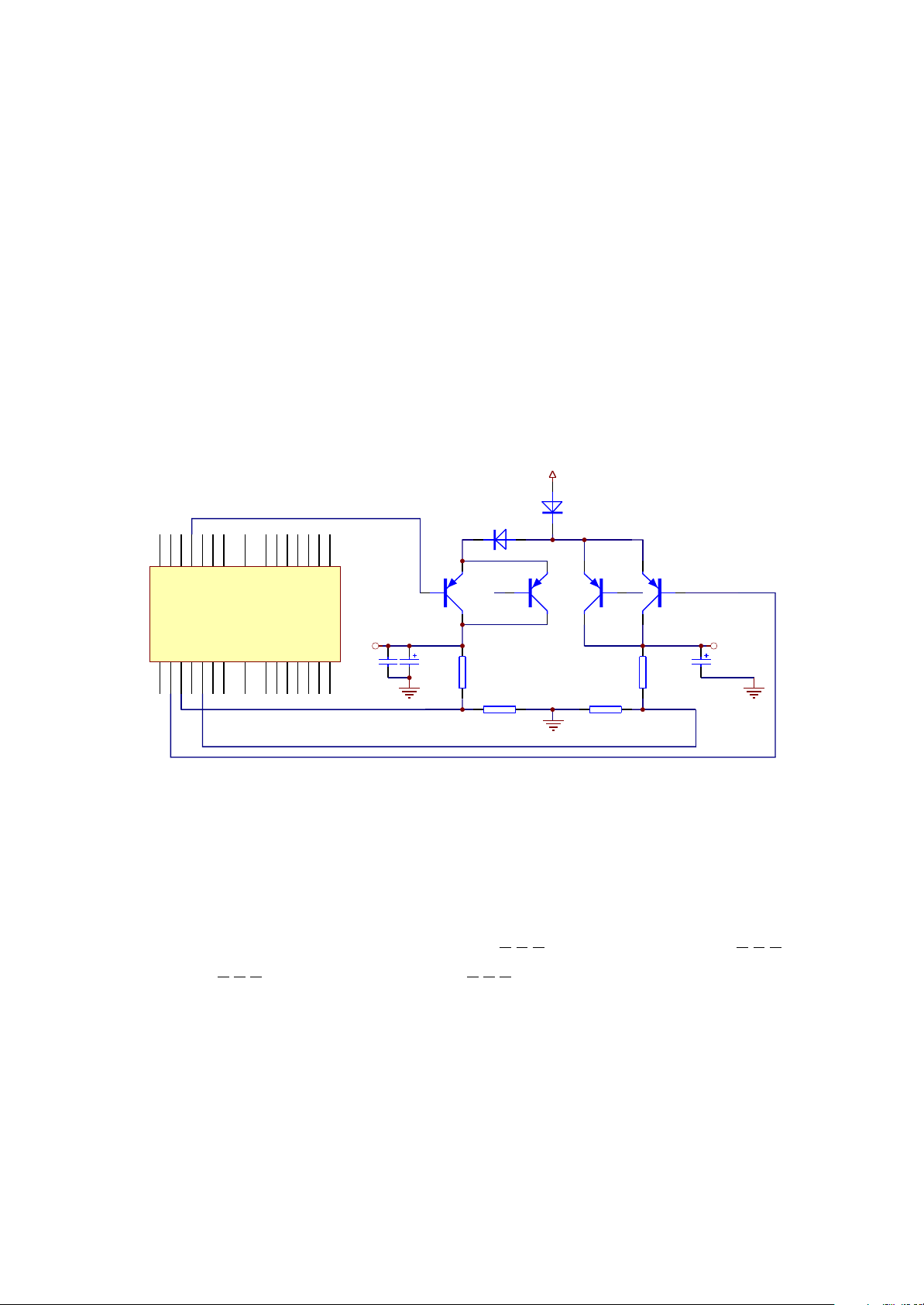
DV113SI
DV123SI
service manual
Page 2

Catalog
Chapter One About Maintenance
1.1 Safety precautions
1.1.1 Power supply
1.1.2 Precautions for antistatic
1.1.3 Precautions for laser head
1.1.4 About placement position
1.2 Maintenance method
1.2.1 Visualized method
1.2.2 Electric resistance method
1.2.3 Voltage method
1.2.4 Current method
1.2.5 Cutting method
1.2.6 Element substitution method
1.2.7 Comparison method
1.3 Required device for maintenance
1
1
1
1
1
2
2
2
2
2
2
2
3
3
3
Chapter Two Functions and Operation Instructions
2.1 Features
2.2 Control Button Locations and Explanations
2.2.1 Front Panel Illustration
2.2.2 Rear Panel Illustration
2.2.3 Display Window Illustration
2.2.4 Remote Control Illustration
2.3 Accessories
2.4 FUNCTION SETUP
2.4.1 Function Setup
2.4.2 Language
2.4.3 Image
2.4.4 Sound
2.4.5 Playback
4
4
4
4
5
5
5
6
7
7
7
7
8
8
Page 3

2.4.6 Preference
9
2.4.7 Parental control
2.4.8 Initial setup
2.4.9 Rest to defaults
2.4.10 Exit
2.5 Specifications
Chapter Three Principle and Servicing
Section One Principle of the Player
3.1.1 Block diagram of the player
3.1.2 PCB board block diagram of the player
3.1.3 How to use IC
Section Two Unit Circuit Principle
3.2.1 Introduction to laser head
3.2.2 Servo circuit
3.2.3 Open/close drive circuit
9
9
9
9
9
11
11
11
12
13
14
14
16
18
3.2.4 Laser power control circuit
3.2.5 CD/DVD conversion circuit
3.2.6 Main axis control circuit
3.2.7 Decode circuit
3.2.8 Reset circuit
3.2.9 Video circuit
3.2.10 Audio circuit
3.2.11 Mute circuit
3.2.12 Decode circuit voltage regulating
3.2.13 Panel control circuit
3.2.14 MIC circuit
3.2.15 Power circuit
Section Three Servicing Cases
3.3.1 Servicing cases
3.3.2 Troubleshooting flow chart
18
19
20
21
22
23
24
25
26
27
27
27
29
29
35
Section Four
Section Five Function Introduction to IC
3.5.1 function introduction to MT1389 D
3.5.2 function introduction to 4558
Waveform diagram
47
53
53
61
Page 4

3.5.3 function introduction to AT24C02
62
3.5.4 function introduction to TDA1308
3.5.5 function introduction to VIPer22ADIP
3.5.6 function introduction to AM5888S
3.5.7 function introduction to PT6961(4dv315)
3.5.8 Function introduction to SDRAM
3.5.9 Function introduction to FLASH
3.5.10 Function introduction to LM431A
3.5.11 Function introduction to Pc817
Chapter Four Disassembly and Assembly Process
Chapter Cinque PCB board & Circuit diagram
Section One PCB board
Section Two circuit diagram
63
64
65
67
68
69
70
71
72
73
73
80
Chapter six BOM List
DV123SI Service Manual
7.1.1 PCB composition figure of the player
7.2.1 Panel control circuit
7.2.2 MIC circuit
7.3.1 PCB board
7.3.2 circuit diagram
87
94
94
95
95
96
100
Page 5

Chapter One About Maintenance
1.1 Safety precautions
1.1.1 Power supply
When maintenance personnel are repairing DVD players, he should pay special attention to the
power board with 220V AC and 330V DC which will cause hurt and damage to persons!
1.1.2 Precautions for antistatic
Movement and friction will both bring static electricity which causes serious damages to integrated
IC. Though static charge is little, when a limited quantity of electric charge is added to large-
scaleintegrated IC, as the capacitance is very small in the meantime, now the integrated IC is very much
easy to be struck through by static electricity or the performance will decrease. Thus static electricity
prevention is of extraordinary importance. The following are several measures to prevent static
electricity:
1. Use a piece of electric conduction metal with the length of about 2 metres to insert into the earth,
and Fetch the lead wire from the top of the surplus metal and connect to the required static electricity
device. The length and depth of the metal embedded under the earth should be determined according to
the wettability of the local soil. For humid places, it may be shorter, and longer and deeper for dry places.
If possible, it can be distributed and layed in terms of “#” shape.
2. On operating table-board, the antistatic table cushion should be covered and grounded.
3. All devices and equipments should be placed on the antistatic table cushion and grounded.
4. Maintenance personnel should wear antistatic wrist ring which should be grounded.
5. Places around the operating position should also be covered with electric conduction cushion or
Painted with antistatic paint.
1.1.3 Precautions for laser head
1. Do not stare at laser head directly, for laser emission will occur when laser head is working, which
will Hurt your eyes!
2. Do not use wiping water or alcohol to clean laser head, and you may use cotton swab.
- 1 -
Page 6

1.1.4 About placement position
1. Never place DVD player in positions with high temperature and humidity.
2. Avoid placing near high magnetic fields, such as loudspeaker or magnet.
3. Positions for placement should be stable and secure.
1.2 Maintenance method
1.2.1 Visualized method
Directly view whether abnormalities of collision, lack of element, joint welding, shedding welding,
rosin joint, copper foil turning up, lead wire disconnection and elements burning up among pins of
elements appear. Check power supply of the machine and then use hands to touch the casing of part of
elements and check whether they are hot to judge the trouble spot. You should pay more attention when
using this method to check in high voltage parts.
1.2.2 Electric resistance method
Set the multimeter in resistance position and test whether the numerical value of resistance of each
point in the circuit has difference from the normal value to judge the trouble spot. But in the circuit the
tested numerical value of resistance is not accurate, and the tested numerical value of integrated IC's
pins can only be used for reference, so the elements should be broken down for test.
1.2.3 Voltage method
Voltage method is relatively convenient, quick and accurate. Set the multimeter in voltage position
and test power supply voltage of the player and voltage of a certain point to judge the trouble spot
according to the tested voltage variation.
1.2.4 Current method
Set the multimeter in current position and test current of the player of a certain point to judge the
trouble spot. But when testing in current method, the multimeter should be series connected in the
circuit, which makes this method too trivial and troublesome, so it is less frequently used in reality.
1.2.5 Cutting method
Cutting method should be combined with electric resistance method and voltage method to use.
This method is mainly used in phenomena of short circuit and current leakage of the circuit. When
cutting the input terminal voltage of a certain level, if voltage of the player rises again, it means that the
trouble lies in this level.
- 2 -
Page 7

1.2.6 Element substitution method
When some elements cannot be judged good or bad, substitution method may de adopted directly.
1.2.7 Comparison method
A same good PC board is usually used to test the correct voltage and waveform. Compared these
data with those tested through fault PC board, the cause of troubles may be found.
Through the above maintenance method, theoretical knowledge and maintenance experience, all
difficulties and troubles will be readily solved.
1.3 Required device for maintenance
Digital oscillograph ( 100MHE)
TV set
SMD rework station
Multimeter
Soldering iron
Pointed-month pincers
Cutting nippers
Forceps
Electric screw driver
Terminals connecting cord
Headphone
Microphone
- 3 -
Page 8

Functions and Operation Instructions
2.1 Features
Compatible Disc Types:
Digital video playback:DVD-Video, Super VCD, VCD Compatibility.
Digital audio playback:CD-DA and HDCD compatibility
Fully compatible with compressed audio files such as Mp3and WMA.
Digital graphic albums playback:kodak picture CD, JPEG compatibility.
Audio:
Coaxial output for Dolby Digital/DTS/LPCM digital audio.
Mixed audio output for amplifier or TV connection.
Digital multi-channel decoders, providing Dolby Digital/DTS audio stream playing.
MIC input for karaoke function.
Video:
108 MHZ/12 bit video Digital/Analog converter.
Composite, S-Video and RGB/SCART outputs for various types of connections.
Capable of playing NTSC/PAL discs.
Multiple dubbings, angles, subtitles support.
Sharpness, gamma, brightness, contrast, hue, saturation adjustment.
Others:
Compatible disc types:CD-R/CD-RW, DVD-R/DVD-RW, DVD+R/DVD+RW
Russia, CIS and Baltic States adaptation interface and filenames, ID3-tags and CD-Text support
simplifies device operation.
"Memory” function enables to save the last point after stop playback.
"Q-play” function provides direct playback and allows to skip commercial that is not possible to
rewind.
"Captrue” function allows to save any picture as background.
"Virtual Keyboard” function provides more convenient DVD playback control.
"Browser” function provides easy access to playback control.
Automatic Screenaver function.
Parental control function to protect children from watching inappropriate discs.
Super wide range of operating power supplies(~110-250V, 50/60Hz), automatic short circuit
protection.
Chapter Two
2.2 Control Button Locations and Explanations
2.2.1 Front Panel Illustration
- 4 -
Page 9
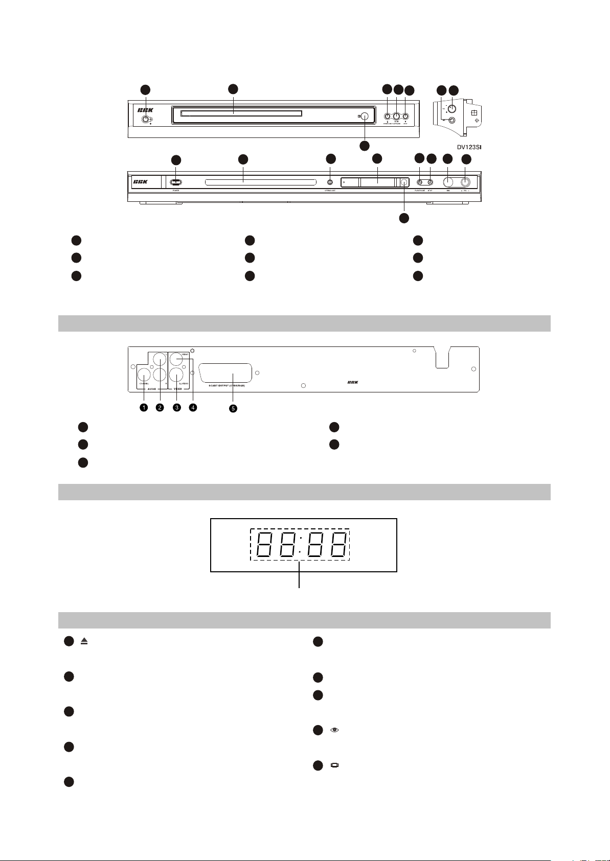
1
1
DV112SI and DV113SI
2
2
3
3
4
5
8
4
6
7
5
6
7
8
2.2.4 Remote Control Illustration
1
POWER switch
2
;Disc tray
3
OPEN/CLOSE button
:
4
5
6
2.2.2 Rear Panel Illustration
1
Digital Audio Coaxial Out jack
2
2CH Audio Out jacks
3
S-Video
2.2.3 Display Window Illustration
Display window*
PLAY/PAUSE button
STOP button
4
5
9
Video Out jack
SCART Out jack
7
MIC jack
8
MIC volume control
9
IR sensor button
2.2.4 Remote Control Illustration
1
[ ]
Button
Open or close the dis tray.
2
LANG Button
Change the audio language or audio channel.
3
MEMORY Button
Save the playing point or jump to the saved point
4
DISP Button
Display or hide disc information.
5
NUMBER Buttons
Playback time
- 5 -
6
BROWSE Buttons
Switch new user interface.
7
CURSOR Buttons
8
SETUP Button
Function Setup.
[ ]
9
Button
Open/close the keyboard function.
[ ]
10
Button
Adjust picture ratio
Page 10
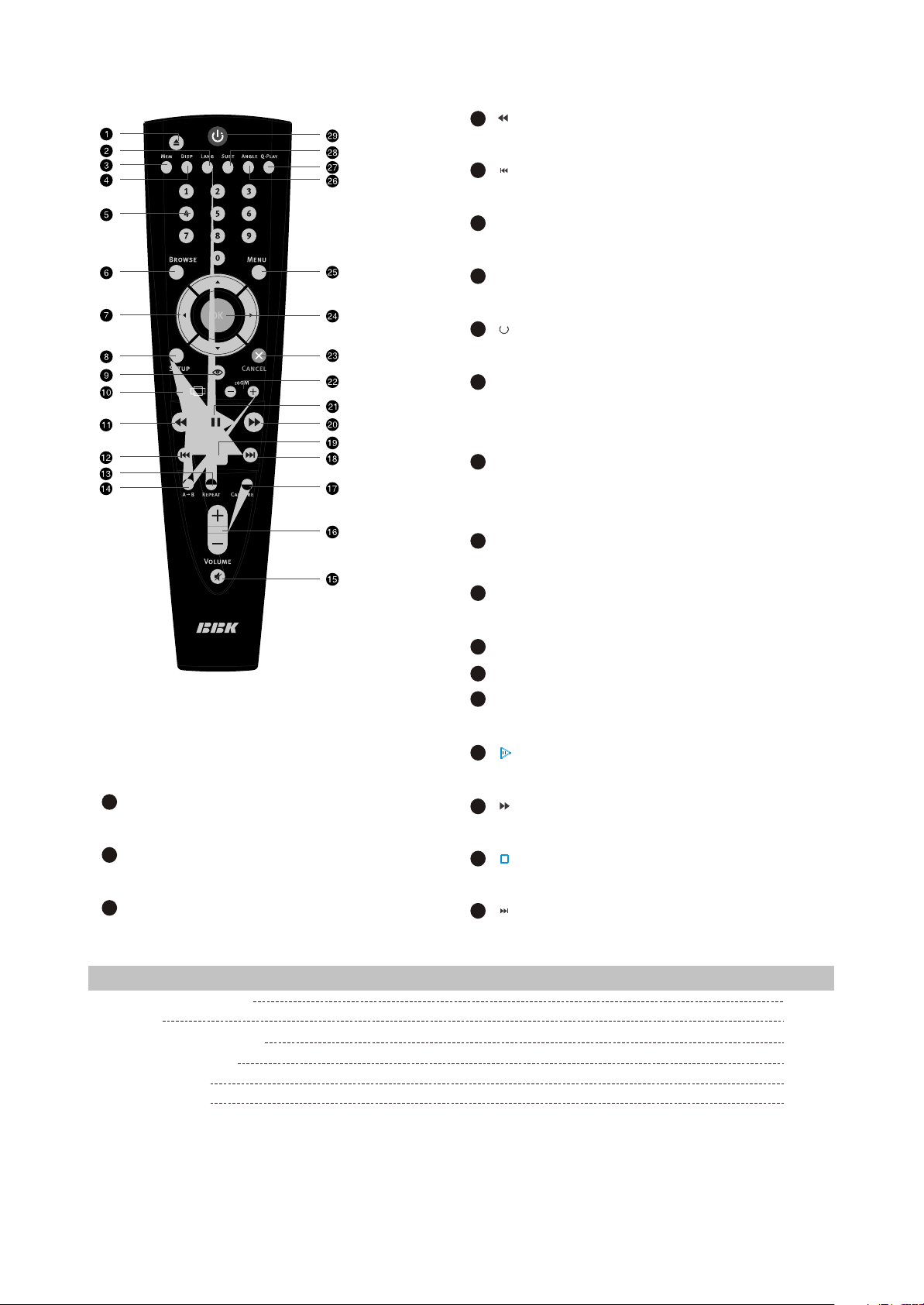
[ ]
11
Button
Fast backward play.
[ ]
12
Button
Skip backward.
13
PEPEAT Button
Repeat play.
14
A-B Button
Repeat the select.
[ ]
15
Button
Press once to stand by, Press twice to play.
16
SUBT Button
Change subtitle language, Switch JPEG
Display mode.
17
Q-PLAY Button
Skip the advertisement/warning and play the DVD
directly.
18
ANGLE Button
27
CAPTURE Button
Set the played image as the Power-on logo.
28
VOL +/- Button
Increase/decrease volume level.
29
MUTE Button
Press once to mute, twice to turn off.
2.3 Accessories
AUDIO/VIDEO CORD
REMOTE
AAA SIIZE BATTERIES
WARRANTY CARD
USER MANUAL
KARAOKE DISC
Change camera angle
19
MENU Button
Display DVD menu or open/close PBC.
20
OK Button
21
Cancel Button
22
ZOOM +/- Button
Zoom in/out the displayed frame.
[ ]
23
Button
.
Play or pause playback
[ ]
24
Button
Fast forward play.
[ ]
25
Button
Stop playback.
[ ]
26
Button
Skip forward.
1PCS
1PCS
2PCS
1PCS
1PCS
1PCS
- 6 -
Page 11

2.4 FUNCTION SETUP
2.4.1 Function Setup
1.Press The [SETUP] Button and The screen
displays the selection Menu of function setup.
Off
Com.
LB
L.
0
0
0
0
LB
L.
Off
0
0
0
0
Setup menu
DVD menu
Soundtrack
Subtitle
AUTO
PAL
NTSC
High
Medium
Low
Off
Language
Image
Sound
Playback
Preference
Parental control
Initial setup
Reset to defaults
Exit
2.Press the [CURSOR] button to select the menu
to be entered and press the [OK] or button to
confirm.Or press the [CURSOR] button to Exit
item and then press the [OK] button to exit .
3.Press [UP/DOWN] arrow to select the desired
item you want to set and press [OK].
For example, press [UP/DOWN] arrows to
select IMAGE and press [OK]. The Image setting
page appears on the screen.
TV system
Video out.
TV format
Sharpness
Gamma
Brightness
Contrast
Hue
Saturation
AUTO
S-Vid.
4.Press [UP/DOWN] arrow to select the
SHARPNESS item. Press [OK] to confirm
it.And then press [UP/DOWN] arrow to select
the desired valus.
For example: Press [UP/DOEN] arrow to
select Medium,then press [OK], the TV screen
display.
TV system
Video out.
TV format
Sharpness
Gamma
Brightness
Contrast
Hue
Saturation
AUTO
5.Press [LEFT] butt on if you not to return to
the previous setup page.
6. Press [SETUP] to exit the setup menu.
2.4.2 Language
Setup menu
DVD menu
Soundtrack
Sbutitles Off
1.Setup menu:This item Is used to se t the
prompts Language on The screen.
Optional setting: Russian, English, Ukrainian.
Default: English.
2.DVD menu: To Set the preference disc Menu
lang when playing.
Optional setting: Russian, English, Estonian,
Latvian, Kazakh, Romanian, Byelorussian,
Ukrainian, Chinese, Others.
Default: English.
3.Sountrack:To set the preference audio
Language when playing.
Optional setting: Russian, English, Estonian,
Latvian, Kazakh, Romanian, Byelorussian,
Ukrainian, Chinese, Others.
Default: English.
4.Subtitles: To Set the preference subtitle
Language when playing.
Optional setting: Off, Russian, English,
Estonian, Latvian, Kazakh, Romanian,
Byelorussian, Ukrainian, Chinese, Others.
Default: Off.
Russian
English
Ukrainian
2.4.3 Image
Off
AUTO
PAL
NTSC
LB
L.
0
0
0
0
TV system
Video out.
TV
format
Sharpness
Gamma
Brightness
Contrast
Hue
Saturation
AUTO
Com.
1.TV system: This Item is used to the video
output system of this unit.
Optional setting: Auto, PAL, NTSC.
Default: AUTO.
2.Video output: To Set the Types of SCART out
connector.
Optional setting: S-Video,Component, SCART,
Default: Component.
When using RGB outputs from the SCART
interface,Please select RGB.Other,please
select Com-and when using S-Video output
please select S-Video.
- 7 -
Page 12

3.TV format: To set the aspect ratio of This player
output image.
Optional setting: 4:3 Pan-scan, 16:9 letterb.
16:9 TV
Default: 16:9 letterb.
4.Sharpness:Used To set the sharpness of video
outputs.
Optional setting: High, Medium, Low.
Default: Medium.
5.Gamma emendation : This item is used To
setup the Gamma value of video output.
Optional setting: High, Medium, Low, Off.
Default: Off.
6.Brightness:Used to set the brightness of Video
outputs.
7.Contrast:Used to set the contrast of Video
outputs.
8.Hue: Used to set the hue of video outputs.
9. Saturation: Used to set the saturation of video
outputs.
Brightness, contrast, Hue and saturation
adjusting means:
A.Press [UP/DOWN] arrow In the video To select
The desired item you want to adjust.Press [OK]
or [RIGHT button] To enter the item's
adjustment.
B.Press [UP/DOWN] arrow to adjust the setting
value.
2.4.4 Sound
Mixer...
Digital output
Tuning
1.Mixer...
Stereo mix
Surr. Mix
A.Stereo mix: To set the output means of the left
or right audio when playing a Dolby disc with
separate two-channel audio.
Optional Setting: L+R, L, R.
Default: L+R.
B.Surr. Mix: To set output means of the surround
left and right audio when playing a stereo disc.
Optional setting: Off, sum, Virt. Surr.
Default: Off.
2.Digital output: select to set the format and
stream form of digital audio output.
A.SPDIF format:
Optional setting: RAW format, SPDIF/PCM.
Default: RAW format.
Stereo mix
Surr. Mix
L+R
off
L+R
off
L+R
L
R
B.LPCM
Optional setting: 48 kHz 16 bit, 96 kHz 24 bit.
Default: 48 kHz 16 bit.
3.Tuning:
A.Max volume: set the maximum volume limit.
B.Equalizer: To set Equalizer modes.
Optional setting: Off, Rock, Pop, Live, Dance,
Techno, Classic, Soft.
Default: Off.
C.Echo: To set different sound field effects.
Optional setting: Off, Concert, Living room,
Hall, Bathroom, Cave, Arena, Church.
Default: Off.
D.Tone balance : to set the tone level to match
your diapason when you're singing
Method to adjust tone control:
a.Press [UP/ DOWN] cursor buttons to select
"tone" item in Audio Setting page, and then
press [OK] or [RIGHT] button to enter
Adjustment Menu.
b.Press [UP/DOWN] cursor button to adjust
setting Value.
C.Press [OK] or [LEFT] button to return to Audio
Setting page after adjustments are done.
2.4.5 Playback
DVD
VCD/SVCD
Files
Repeat
Load effect
1.DVD: set whether information of advertisement
and warnings at the beginning of DVD disc is
skipped to play the movie directly.
Always skip ads
Optional setting: Yes,
Default: Number
2.VCD/SVCD: To set the PBC status.
When playing Super VCD or VCD2.0 discs, if
the PBC Is ON, The menu image displays
Optional setting: On, Off.
Default: On.
3.Files: data disc may probably includes Mp3,
JPEG format files in which you may select DVD
player to read the file type.
Optional setting: Audio, Picture.
Default: Audio, Picture.
4.Repeat : select the repeat playback mode.
Optional setting: Off, Single, all.
Default: Off.
5.Load effect: set the may to play JPEG image.
Optional setting: Off, from top, from bottom.
Advertisemenu No
A. P
Off
Off
- 8 -
Page 13

Default: Off.
Playable discs
Inputs
DVD-Video, Super VCD, VCD, CD-DA, CD+G, HDCD, MP3, Kodak
piclure CD, JPEG
MIC INPUT
2.4.6 Preference
Gr. equalizer
Background
Screen saver
Off
std.
On
On
Off
Old password
New password
Verify
OK Cancel
1.Gr. equalizer: This item is used to set wether
the Dynamic Spectrum is allowed.
Optional setting: On, Off.
Default: Off.
2.Background: This item is used ti setup the sort
of Power-in Logo.
Optional setting: Standard, saved.
Default: Standard.
NOTE
The Screen Logo refers that use the image
selected by pressing the [CAPTURE] button as
the power-on logo.When in the operation of
changing screen, if the power -on logo has not
set in Screen Logo, the unit will automatically set
the power-on logo as screen logo.
3.Screen saver: Open or close the screen saver
function.
Optional setting: On, Off.
Default: On.
2.4.7 Parental control
Any
Kid
G
Allowed..
Set password
Any
1.Allowed..: To set the parental control ratings to
prevent children from watching the restricted
contents.( In case the disc supports this
function.)
Optional setting: any, Kid, G, PG, PG-13, PGR,
R, NC-17.
Default: any.
2. Set password: To set four digit password to
enable you to change the parental control
ratings.
Default: 7890.
PG
PG-13
PGR
R
NC-17
2.4.8 Initial setup
Auto
PAL
NTSC
Press [UP/DOWN] arrow to select the
desired option and press [OK] button to confirm it.
NOTE
In this setup state, you may not press [LEFT]
button to return to the previous menu.
2.4.9 Rest to defaults
Load factory settings
OK
Cancel
Reset to defaults: To restore all settings to
the default Value except for the parental control
and password settings.
2.4.10 Exit
Language
Image
Sound
Playback
Karaoke
Preference
Parental control
Initial setup
Reset to defaults
Exit
Press [UP/DOWN] arrow to select the Exit
item. Press [OK] button to exit the setup menu.
2.5 Specifications
- 9 -
Page 14
Audio outputs
Video outputs Composite, S-Video RGB/SCART
Video characteristics
Audio characteristics
Operating voltage
Power Consumption
General Specification
Dimensions:
Mass:
DU112SI, DV113SI
320×224×41mm
1.7kg
DV123SI
420×275×47mm
2.3kg
Operating temperature
Operating humldlty
Outputs
20W
5 -35
15%-75%(no conden sation)
Analog audio output: Stereo
Digital audio output: Coaxial
Video amplitude: 1.0Vp-p(75 )
S-Video amplitude: Y:1.0Vp-p(75 ) C:0.286Vp-p(75 )
Frequency response 20-20000Hz(±1dB)
Signal-to-noise ratio >100(dB)
THD <0.01%
~100V-250V, 50/60Hz
Design and specifications are subject to change without notice.
We do not guarantee that all discs can be played smoothly due to the disc quality, disc recording
quality and recording format.
- 10 -
Page 15
Chapter Principle and Servicing
Section One Principle of the Player
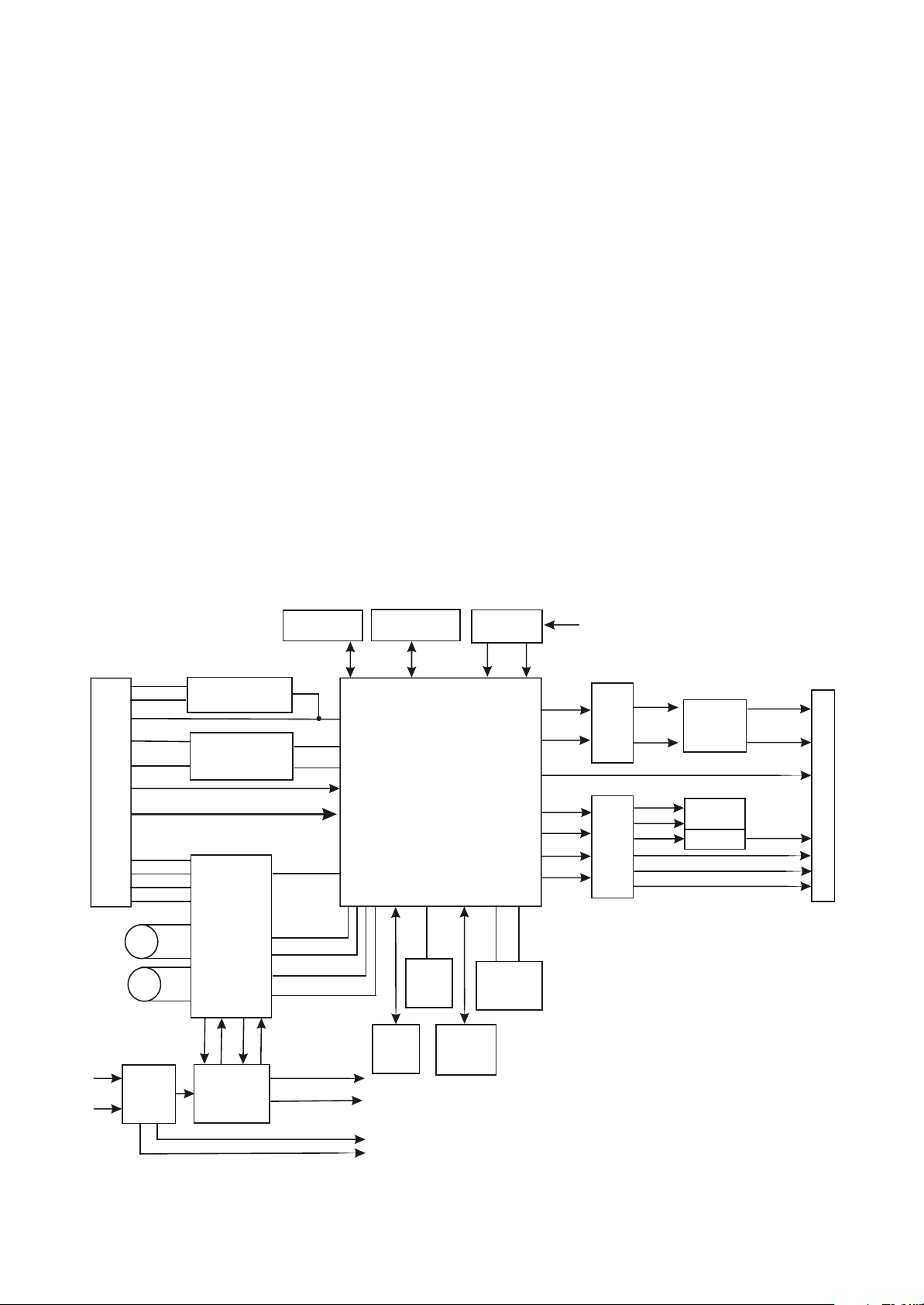
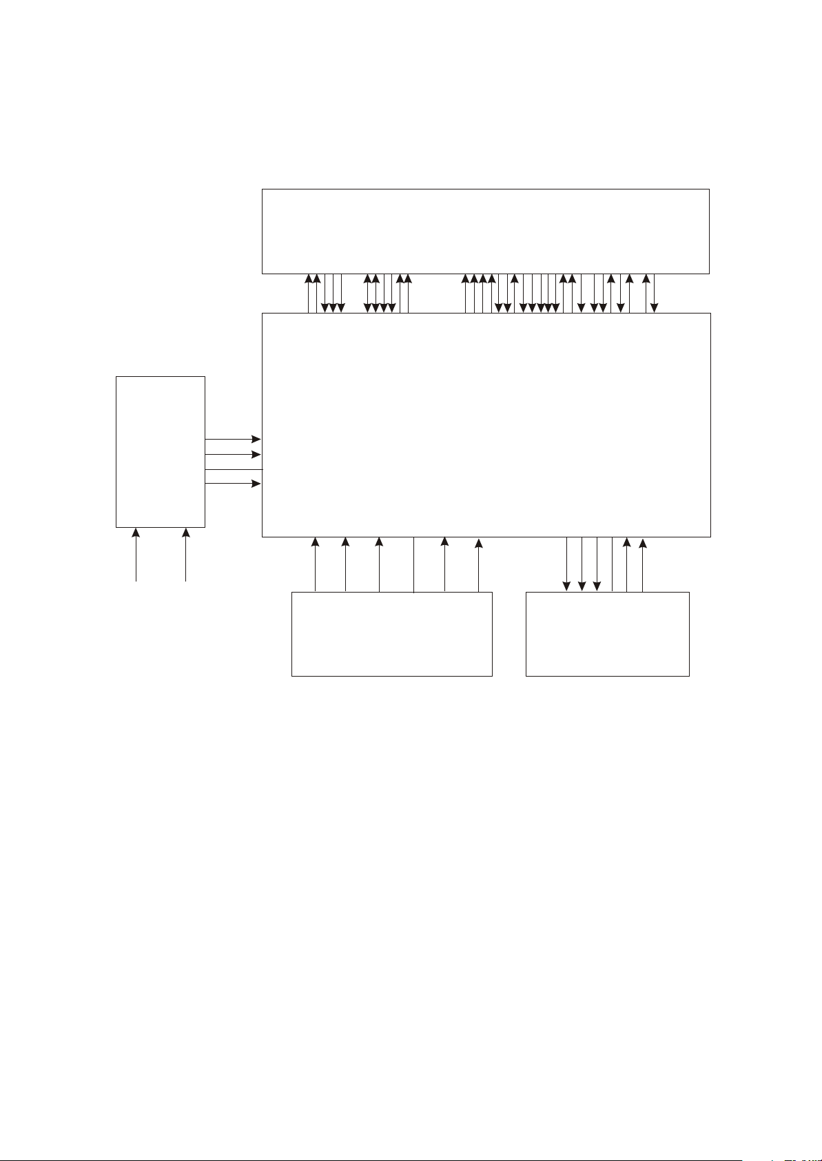
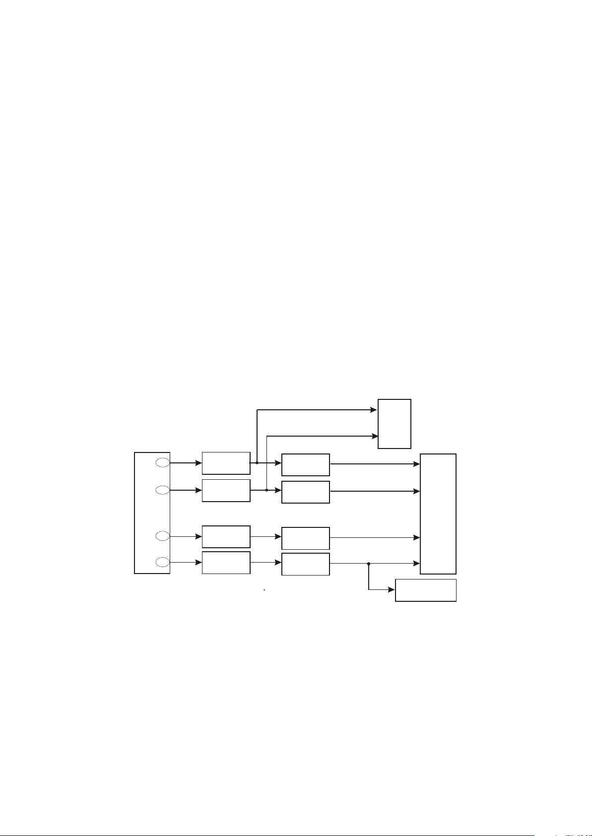
3.1.1 Block diagram of the player
DV317SI is composed by decode circuit, servo circuit, audio circuit, video circuit, MIC circuit and
power circuit, the block diagram of the player is shown as in the following figure 3.1.1.1:
PICK-UP
Feed
electric
machine
Main
axis
electric
machine
ACIN
VR-DVD
VD-CD
LD-DVD
LD-CD
TK-
TK+
FC+
FC-
SL+
M
M
SL-
SP+
M
SP-
Power
board
CD/DVD switch
Laser power
control
DVD:A/B/C/D/RFO
CD:A/B/C/D/E/FRFO
Am5888
U301
TRB2
TRB1
REGO1
Voltage
regulating
circuit
SDRAM 64M
U208
Ld02
Ld01
MDI
VIP4
FOSO
FMSO
DMSO
TRSO
REGO2
V18
Dv33
+9V
IOA
FLASH16M
U207
MT1389 D
U201
UREST
Reset
Panel
MIC board
XI
SDA
SCL
27M clock
EEPROM
U202
24C02
XO
MIC1
AL
AR
CVBS
Y/G
CB/B
CR/R
Audio
amplifying
filtering
U209
CVBS
B/U
R/V
G/Y
Video filtering
catching
L
R
SY
SC
Audio
output
terminal
S-video
Terminal
Video output
L#
R#
SPDIF
VIEDO#
PB#
PR#
Y#
SCART output terminal
-9V
Figure 3.1.1.1 Block diagram of the player
- 11 -
Page 16
3.1.2 PCB board block diagram of the player
PCB board block diagram of the player is show as in the following figure 3.1.2.1:
Power board
5241-0
BCN501
AC220V
IOA
C
D
Laser head
RFO
ABF
F
A
B
IOA
RFO
XS301
GND
V20
V20
GND
+5V
E
VR-CD
AVCC
E
AVCC
VR-CD
XS205
_9V
+9V
XS601
VR-DVD
CD-LD
MDI
CD-LD
VR-DVD
GNDOKDET
HFM
DVD-LD
GND-LD
MDI
HFM
DVD-LD
GND-LD
Loader frame Small bracket
FC-
FC+
TK+
LOAD-
LOAD+
TROUT
LOAD-
LOAD+
TROUT#
SL+
SL-
LIMIT#
GND
SP+
GND
TRIN
GND
TRIN#
SP-
SL-
SP-
SL+
SP+
GND
LIMIT#
TK-CD
TK-
FC-
TK+
FC+
XS307 Xs306
CN501
+12V
-12V
GND
VCC
XS203
Decode board
2DV112S-0
Xs201
2
VSDA
3
VSCK
4
6
5
GNDVSTB
VCC
7
IR
Main panel
4911S-1
MIC board
6112S-2
Figure 3.1.2.1 PCB board block diagram of the player
This machine is mainly composed of decode board, power board, MIC board, main panel buildup
Decode board: includes decode, servo, audio, video output circuit.
Power board: provides working voltage for each circuit, output voltage has +12V, -129V and +5V.
MIC board: with single-way microphone input, MIC signals input to decode board after being
amplified.
Main panel: this panel is simple and mainly composed of remote control receiver and buttons.
Remark: in order to facilitate readers to better know the composition of machine, we have made
PCB composition figure, the connecting lines in PCB composition figure are the main control line, signal
line and power cord connected through flat cable, but all connected flat cable are not included.
- 12 -
Page 17
3.1.3 How to use IC
Semi-finished PCB
name
IC model name Location Function
AZ431 U503 Precise voltage regulator
PC817 U502 Photoelectric coupler
VIPER22A U501 Power switch IC
Main panel 4911S-1 HS0038B3V U403 Remote control receiver
OK board 6112S-1 KA4558 U601
Operational amplifier (MIC
amplifying)
NJM4558 U219
Operational amplifier (audio
amplifying)
HY57V641620HGT-7 U206 SDRAM
24C02 U202 EEPROM
MT1389 D version U201 Decode chip
AM5888S U301 Servo drive
29LV160BE U214 FLASH
Decode board
2DV112 S-0
Power board
5241-0
DV112SI IC usage instruction is shown as in the following table:
- 13 -
Page 18
Section Two Unit Circuit Principle
Pin Name
Signal flow
direction
DVD disc CD disc No disc Function description
1 F- Input loader 2.52 2.34 0.46
2 F+ Input loader 2.49 2.49 0.93
3 T+ Input loader 2.53 2.51 0.94
4 T- Input loader 2.58 2.51 0.93
5 C Input MT1389 2.2 2.25 2.04 Disc data signal
6 D Input MT1389 2.2 3.2 2.04 Disc data signal
7 IOA Input MT1389 0.01 3.2 3.21
Disc identification signal, CD is 3.3V, DVD
is 0V
8 RF Input MT1389 2.21 2.53 1.28 The sum of disc data signal
9 A Input MT1389 2.17 2.22 2.04 Disc data signal
10 B Input MT1389 2.19 2.27 2.04 Disc data signal
11 F Input MT1389 2.07 2.44 2.03 Supplementary signal used in trace
12 GND Ground 0.01 0.01 0 Grounding
13 V20 Input loader 2.04 2.06 2.03 Reference voltage
14 Vcc Input loader 5.04 5.04 5.02 Supply voltage for loader
15 E Input MT1389 2.06 2.45 2.03 Disc data signal
16 Blanking haning in air 0.01 0 0 unused
17 VR-CD Input loader 0.21 0.01 0
Through the handling inside loader, make
sure MD11 is 180mV when reading CD
18 VR-DVD Input loader 0.01 0.2 0
Through the handling inside loader, make
sure MD11 is 180mV when reading DVD
19 LD-CD Input loader 0.09 2.1 0 CD laser power control signal
20 MDII Input MT1389 0.21 0.2 0 CD and DVD laser power monitoring signal
Focus error signal is added to two sides of
pick-up focus coil
Trace error signal is added to two sides of
pick-up trace coil
3.2.1 Introduction to laser head
Function introduction to laser head flat cable is shown as the following table:
- 14 -
Page 19

Note: 1. When reading DVD, there are only A, B, C, D signals.
Pin Name
Signal flow
direction
DVD disc CD disc No disc Function description
21 HFM Input loader 5.04 5.04 5.02
High frequency overlapping signal produces
laser with different wave length inside
loader
22 Blanking unused 0.01 0.1 0
23 LD-DVD Input loader 2.21 0.1 0 DVD laser power control signal
24 GND unused 0.01 0.01 0 Grounding
2. When reading CD, there are A, B, C, D, E, F signals.
3. RFO=A+B+C+D.
4. Focus error signal=(A+C)-(B+D) Trace error signal=E-F.
2. Working principle
(1) Laser tube: wave length of loader DVD laser diode is 650nm, wave length of CD laser diode is
790nm, the wave length which is within 370nm and 750nm is visible light, the laser in the course of
reading DVD disc is visible light, and that when reading CD disc is infrared light.
(2) Principle about laser head picks up signal: laser beam projects onto disc, when laser beam focus
projects onto disc vertically, laser beam will produce reflection, reach on light sensor through reflection
loop and converse into electronic signal through photoelectric cell. For the reflection loop produced in
non pit information area and pit information area in disc has difference and reflects into different position
of light sensor, photoelectric diode in different positions on light sensor will produce different signals to
process all signals on light sensor and then produce digital signals.
(3) Focus, trace coil: when laser head is reading signals normally, information side should be in the
focus of laser beam, because of factors of disc error, high speed rotation and machine error, it is
unavoidable that laser beam focus deviates from information face to produce phenomena of orbit boas
and refocusing. Focus , trace coil is added on loader to adjust laser beam to make it correctly focus in
information area.
(4) Formation of RF signal: when disc reading is normal, light sensor will have 160MV, vague and
eye pattern waveform which is added on A, B, C, D respectively, and output RF signal from FRO pin after
being overlapped by adder inside light sensor, the frequency when reading DVD disc is much higher
than that when reading CD disc, output amplitude is about 1.4V.
- 15 -
Page 20
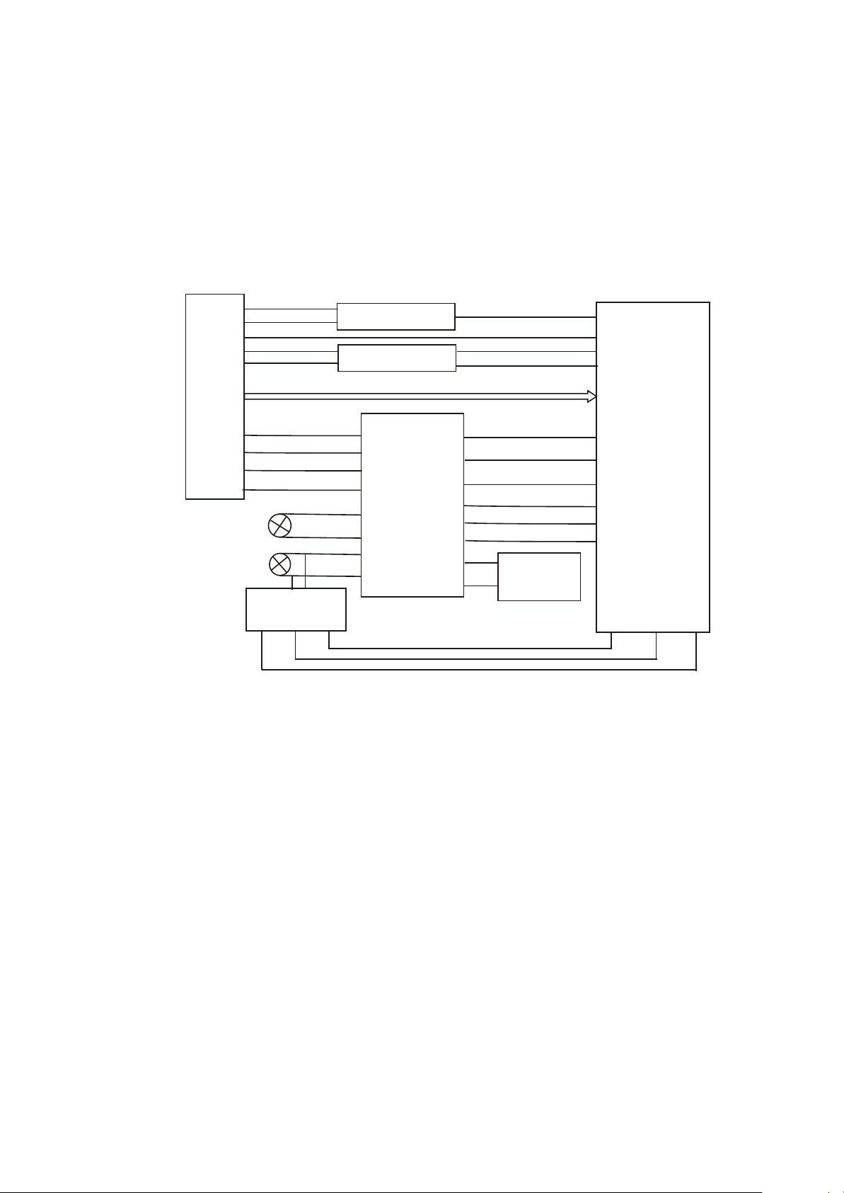
3.2.2 Servo circuit
1. Servo system of this player adopts SANYO loader + MTK decode solution (MT1389D+FLASH
(16M) + SDRAM (64M)), and its servo circuit is mainly composed of front end signal processing, digital
servo processing, digital signal processing IC MT1389D and drive circuit AM5888S , in which MT1389D
is also the main composed part of decode circuit. Servo circuit block diagram is shown as in the
following figure
Feed electric machine
Main axis electric machine
3.2.2.1:
Xs301
A B C D E F RFO
TK+ 16
FC+ 14
FC- 13
SL+ 17
Main axis control
detect circuit
Switch circuit
APC circuit
TK- 15
SL- 18
SP- 12
SP+ 11
Am5888
LOAD+
LOAD-
1
23
26
4
7
6
FOSO
FMSO
TRSO
DMSO
TRCLOSE
TROPEN
10
Disc in/out
9
electric machine
IOA
MD11
LDO2
LDO2
MT1389D
U201
Figure 3.2.2.1 Servo circuit block diagram
2. Working principle
After power on or disc in to proper position (on loader frame for general DVD players, on PCB board
below door for PDVD players), loader laser head begins reset, after laser head reaches to proper
position, detect switch will give a signal to MT1389, MT1389 begins to output focus, main axis and light
emission signals, disc begins to rotate, laser head begins to recognize disc information and judge
whether disc is CD or DVD according to disc information to facilitate to output level from IOA pin, control
disc switch circuit and laser head PD IC to make corresponding acts. At the same time, MT1389 also
adjusts laser power output through laser power control circuit.
After loader reads disc information, A, B, C, D, E and F signal are formed through photoelectric
conversion to MT1389 (DVD only has A, B, C, D signals) and RF signal and output from pin 2~11, 18, 19
of MT1389 respectively, after amplifying processing of pre-amplifier inside MT1389, now signals are
divided into 2 ways inside MT1389: one part, through summation amplifying and subtraction circuit
- 16 -
Page 21

Inside MT1389, produces servo error signal, after digital servo signal circuit processing, forms
corresponding servo control signals, outputs FOO, TRO, DMO and FMSO servo control signal from pin
42, 41, 37 and 38 of MT1389 respectively and then send to servo drive circuit for drive amplifying
through the integration circuit composed by resistor and capacitor and bring along focus coil, trace coil,
main axis electric machine and feed electric machine after drive amplifying. Among these, focus and
trace servo are used to correct objective position accurately; feed servo is used to bring along laser
head to make radial large-scale move which belongs to the preliminary adjustment to laser head
position; and main axis servo is used to control main axis electric machine to make it read signals in
means of constant linear velocity and bring along disc to rotate. After processing of amplification by VGA
voltage control amplifier and equalization frequency compensation inside MT1389, another part of
signals are changed into digital signals through internal A/D converter. When loader is reading CD/VCD
signals, these signals are conducted EFM demodulation inside MT1389, and then outputted to latter
stage for AV decoding after finishing CIRC (Cross-Interleaved Reed-Solomon Code) error correction
inside. When loader is reading DVD signals, these signals are conducted ESM demodulation inside
MT1389, and then sent to latter stage for decoding after finishing RSPC error correction inside. General
DVD players have a disc in/out circuit to control disc tray door in/out acts to reach the purpose of making
disc in and out. For PDVD, we adopt manual disc in/out means and we can judge whether disc in to
proper position through detect switch.
3. Explanation to servo terms
(1) FOO: for disc make differences, and when rotating disc may probably move upwards or
downwards slightly to make the focus of laser emitted by laser head cannot justly fall on data pit of disc,
now focus point of objective lens is required to adjust to make focus aim at data pit exactly. The acts are
mainly to make objective lens move upwards and downwards.
(2) TRO: data information is saved in disc in form of tracks. When disc is rotating, disc deviation will
produce, now laser head is required to adjust. In this process, objective lens makes forward and
backward movement with small moving range.
(3) FMO: similar to acts of trace, the acts of feed are larger than those of trace. Feed conducts a
large scale movement firstly, and then trace moves slightly in this range. Feed moves for a while, and
does not move for another while; but trace moves all the time. Feed is rough adjustment and trace is fine.
And acts are obvious when power on and selecting track.
(4) DMO: it is the top that holds up disc. Its rotation speed decides that of disc. Its rotation is
generated by an individual DC electric machine, in which rotation speed of DVD is twice over that of CD.
- 17 -
Page 22
3.2.3 Open/close drive circuit
1. Open/close drive circuit is shown as in the following figure 3.2.3.1:
27K
TRSO
FC+
FCSPSP+
LOAD+
LOAD-
TKTK+
SL+
SL-
AM5888S
Figure 3.2.3.1 Open/close drive circuit diagram
STBY
V1P4
FMSO
TRCLOSE
TROPEN
DMSO
FOSO
2. Working principle: when the machine is reading discs normally, pin 6, 7, 9 10 of AM5888S are all
0V. After OPEN button is pressed, pin 6 inputs high level, pin 10 LOAD+ outputs high level, electric
R203
R202
R314
10K
R204
15K
MT1389D
R201
10K
27K
machine rotates to perform OPEN acts. When closing, pin 9 LOAD- outputs high level to pin 9 through
electric machine to form loop, electric machine rotates reversely to perform CLOSE acts. After closing to
proper position, all pins are all low level. Servo drive principle is the same with the drive of D5954
scheme, so we will not describe here.
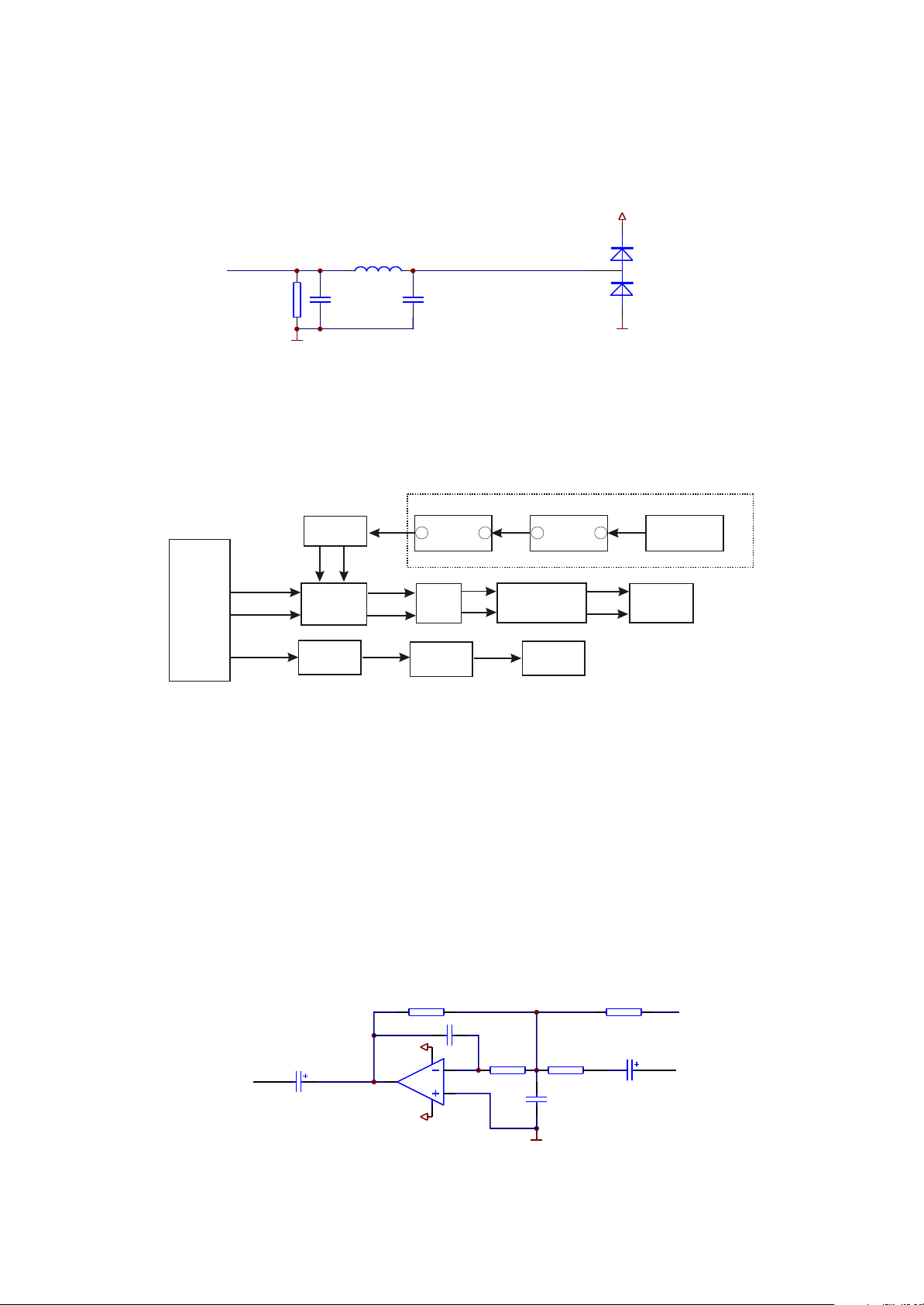
3.2.4 Laser power control circuit
Laser power control circuit is shown as in the following figure 3.2.4.1:
LDO-AV33
4.7R
TC302
47uF/16V
LDO2
V301
2SB1132-S
20/21
MT1389D
V302
2SB1132-S
LDO1
XS301
R301
23
MD1
20
19
TC303
47uF/16V
4.7R
R302
Figure 3.2.4.1 Laser power control circuit diagram
LDO-AV33
- 18 -
Page 23
2. Working principle
Location number Read DVD disc Read VCD disc Location number Read DVD disc Read VCD disc
V301_E 2.9V 3.2V V302_B 3.2V 2.2V
V301_B 2.2V 3.2V V302_E 3.2V 2.9V
V301_C 2.2V 0 MT 1389_20 0.2V 0.2V
V302_C 0 2.2V
Pin 20/21 of MT1389 is laser power detect signal input pin, pin 21 is DVD laser power strong/weak
detect signal input pin, pin 23 is VCD laser power drive control output pin, pin 22 is DVD laser power
drive control output pin.
When reading VCD disc, laser power becomes weak, voltage of MDII pin decreases, voltage
decrease of pin 23 of MT1389 makes voltage of pin 19 of XS301 increase to reach the purpose of raising
laser power. When laser power is too strong, voltage of MDII pin increases to lead to voltage of pin 23 of
MT1389 increase to make voltage of pin 19 of XS301 decrease to reach the purpose of reducing laser
power to form an auto power control circuit.
When reading DVD disc, pin 21 is detect signal input pin, pin 22 is drive control input pin, and the
working principle is the same with that when playing VCD disc.
3. Key point voltage (unit: V) is shown as the following table:
3.2.5 CD/DVD conversion circuit
1. CD/DVD conversion circuit is shown as in the following figure 3.2.5.1:
AVCC
V305
3904-S
R309
10K
R311
10K
R310
100K
IOA
MT1389D
R308
100K
XS301
V303
17
2SK3018-S
18
Figure 3.2.5.1 CD/DVD conversion circuit diagram
V304
2SK3018-S
2. Working principle
After loading disc in the player, IOA port of MT1389 is defaulted high level to make V305 saturation
on and form loop together with CD laser power control circuit on CD. At the same time, IOA also goes to
- 19 -
Page 24
Base
electrode B
Collector C Em itte r E
Grid
electrode G
Drain
electrode D
Source
electrode S
G D S IOA
DVD disc 0 3.86 0 3.81 0.18 0 0 0 0 0
VCD disc 0.64 0.1 0 0 0 0 3.27 0.18 0 3.3
State
V305 V303 V304
Loader PD IC to switch, disc begins to rotate, when servo management system recognizes that the disc
in player is not CD disc, IQA pin outputs low level to make V305 cut off and make V303 on, and form loop
together with DVD laser power control circuit on loader to perform disc reading acts. After disc tray door
opens, IOA keeps the state before opening disc tray door. If the player cannot recognize which disc it is,
IQA pin will switch continuously until reading disc or system judges that there is no disc.
Note: V303 and V304 are MOS tube
3. Key point voltage (unit: V) is shown as the following table:
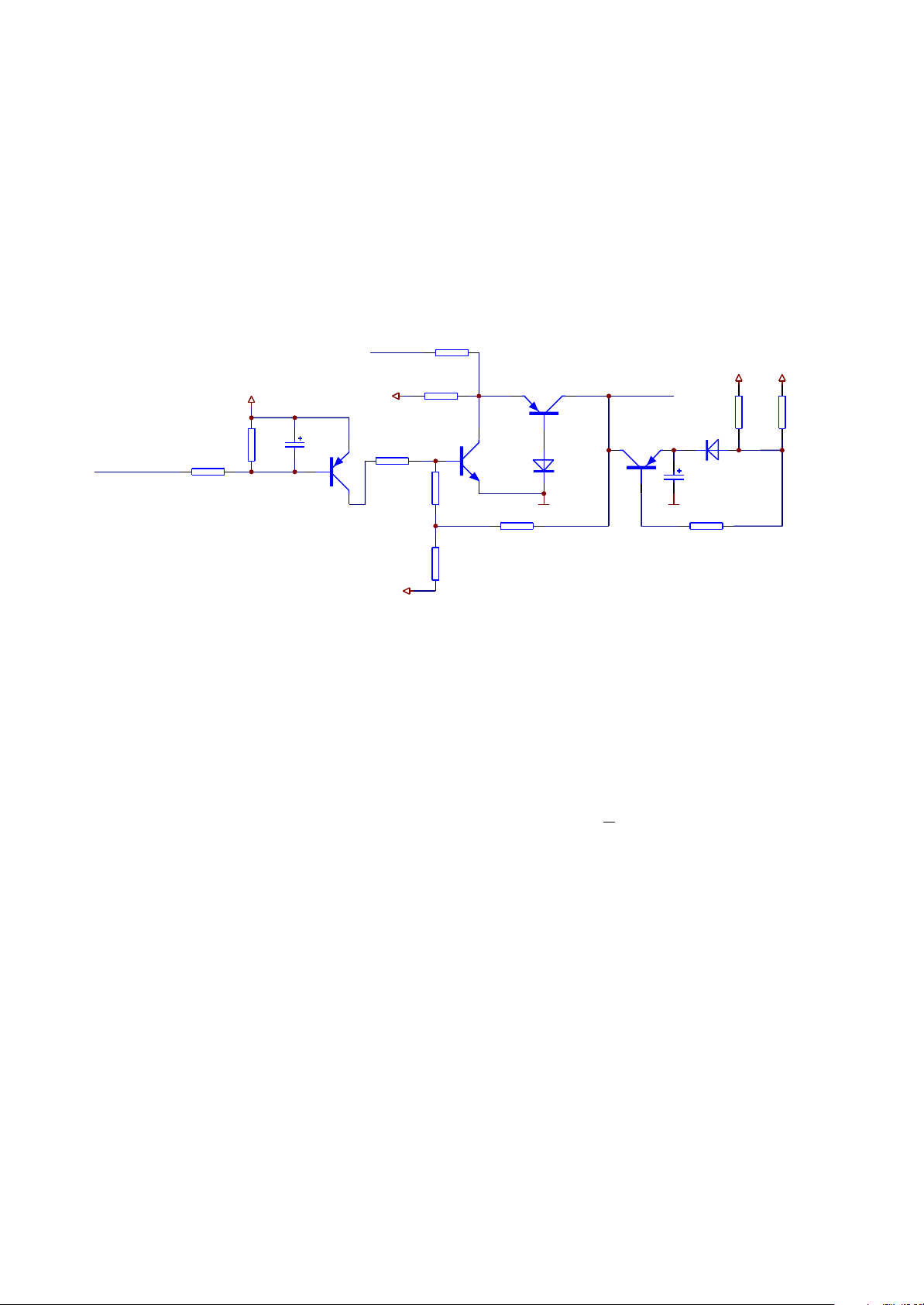
3.2.6 Main axis control circuit
1. Main axis control circuit is shown as in the following figure 3.2.6.1:
XS303
6P2.0mm
R330 10K
1
2
3
4
5
6
104
C313
R321
R319
150K
Figure 3.2.6.1 Main axis control circuit diagram
DV33
SL+
SL-
LIMIT#
SP+
SP-
1R
680K/1%
R320
150K
R318
R322
330
C307
LIMIT
222
R317
680K/1%
C308
101(DNS)
C310
222
R331
0R
OPO
ADIN
OPOP+
V1P4
2. Function: disc is always in high speed rotation in the course of disc reading, when you need to
open the door to change disc, MT1389 stops the positive direction drive signal which is given to main
axis drive circuit, for the function of inertia disc is still rotating. If disc out order is performed at this time,
disc will be abrasively damaged. Therefore, machine must be baking to main axis, that whether disc
hasstopped rotating and whether disc is reversing, decode chip of the machine cannot recognize. So a
main Axis control circuit is added to make decode chip can effective monitor that whether disc has
stopped rotating.
3. Working principle: MT1389 has a comparator inside composed of operational amplifier, in which
OP+ is the in-phase input end of operational amplifier, OP- is reverse input end, OPO is output end,
- 20 -
Page 25
When playing disc normally, for electric machine is positive direction rotating, voltage of OP+ is higher
Key point Position Normal working voltage (V) Volateg change when disc out (V)
SP+
Pin 11 of AM5888S, pin 5 of
XS307
3.79 3.79 0.70 1.80
SP-
Pin 12 of AM5888S, pin 6 of
XS307
1.38 1.38 3.40 1.80
OP+ Pin 36 of MT1389 1.38 1.38 3.10 1.80
OP- Pin 35 of MT1389 1.53 1.53 3.08 1.98
OPO Pin 34 of MT1389 2.44 2.44 0.40 2.50
AD IN Pin 47 of MT1389 2.44 2.41 0.41 2.44
DMSO Pin 4 of AM5888S 1.42 1.42
VIP 4 Pin 30 of MT1389 1.41 1.41
than that of OP-, voltage of OPO is more than 1.4V. When disc out is needed, main axis drive signal
stops, for electric machine is permanent magnetic, when in rotating, induced electromotive force
produces in two ends to give to decode chip through R320, R319 sampling to make OPO output less
than 1.4V voltage and transmit to input pin of MT1389 ADIN through R331. When ADIN is high level,
main axis drive output end has not any drive signal output, when ADIN is low level, MT1389 outputs a
reversing drive signal to main axis drive circuit to make main axis electric machine speed down. Thus
circular working goes on until main axis stops rotating. PDVD is manual disc out means, so after disc out,
disc is still rotating, but will stop very son.
4. Key point voltage (unit: V) is shown as the following table:
3.2.7 Decode circuit
1. Decode circuit block diagram is shown as in the following figure 3.2.7.1:
2. Working principle: this decode circuit is mainly composed of MT1389, SDRAM and FLASH.
Working condition of decode circuit has:
(1) Reset: refer to reset circuit working principle for details.
(2) Clock: this system adopts 27M external clock input, and produces clock signal required by
system inside through internal frequency doubling circuit.
(3) Power: decode chip adopts twp groups power supply of 3.3V and 1.8V, in which 1.8V mainly
supply power for internal logic control circuit and we call it core voltage.
After power on, reset circuit performs reset to MT1389 built-in CPU (8032) and FLASH, decode chip
outputs reset signal at the same time and performs reset to other circuit. After system reset, it firstly
Sends out read signal to FLASH to read out in formation saved in FLASH, the machine displays power-
on picture, servo system begins to work to check whether machine closes door to proper position and
- 21 -
Page 26
FLASH
PWR
PRD
PCE
A0~A20
AD0~AD7
URST
MT 1389
SDCLK
SDCKE
DCS
DRAS
SWE
DQM0
DQM1
DQ0~DQ15
MA0~MA11
SDRAM
Reset
circuit
SDA
SCL
EEPROM
24C02
Figure 3.2.7.1 Decode circuit block diagram
Clock
27M
V18
1.8V
voltage
regulating
3.3V
voltage
regulating
Whether detect switch has been closed, if not, the door close action is performed. After detect switch of
door is closed, the machine begins to perform preparations of disc reading and performs panel display
at the same time of working.
Playback process: laser head picks up disc signal from disc, after servo system processing, then
send to decode circuit for decoding, signal after being decoded is saved in SDRAM for the moment.
When machine needs to replay signal, decode circuit calls information inside SDRAM to perform D/A
conversion and then output.
User information storage: information content set by user is saved inside EEPROM, if user does not
refresh or reset this information, it will saved in IC permanently.
Audio, video output circuit: at present, MT1389 all integrates video D/A converter, MT1389D inside
integrates audio D/A converter, manufactures select according to their own needs. Please refer to
circuit principle diagram and audio circuit explanation for details.
3.2.8 Reset circuit
1. Reset circuit is shown as in the following figure 3.2.8.1:
DV33
R254
10K
V310
33R
R255
C272
104
URST#
1N4148
VD201
TC217
106
2SC1815-YS
R250
1K
R252
47K
Figure 3.2.8.1 Reset circuit diagram
- 22 -
Page 27
2. Working principle: after power on, voltage of DV33 increases to 3.3V, main chip power supply is
normal. Now, voltage of TC217 to DV33 cannot change suddenly to make base electrode of V310 has
current flow in, V310 is saturation on, URST is low level. DV33 charges TC217 in two paths through
emitter junction of R252 and V310 make negative pole voltage of TC217 decrease slowly. When this
voltage decreases below 0.7V, V310 cuts off, URST changes into high level, the process for URST from
low to high is called effective reset signal of low level by us. After power off, voltage of DV33 decreases,
TC217 decreases together with DV33 voltage, VD201 performs suge discharge and clamping to Tc217.
3. Key point voltage (unit: V)
V310_B is low level when in normal condition, at the moment of power on, it decreased to 0V from
3.3Vgradually.
V310_C is high level when in normal condition, at the moment of power on, it increases to 3.3V from
0V.
3.2.9 Video circuit
1. Video signal flow chart diagram is shown as in the following figure :
SY
SC
Y4
179
Y5
181
MT1389
Y6
182
Y3
175
L212
L213
L214
L210
R/V/SY
CUBS
Figure 3.2.9.1 Video signal flow chart
L240
L239
L241
R284
CUBS#
3.2.9.1
S-Video
Jk202A
11
7
SCART
Terminal
15
19
Jk202B
CVBS -Video
2. Working principle: MT1389D has built-in video D/A conversion circuit, video output has R/B/G
Y/Pb/Pr Y/Cb/Cr CVBS Y/C output mode, in which R/B/G Y/Pb/Pr Y/Cb/Cr Y/C cannot output at the
same time and need the switch through software. CVBS is a separate output mode, 4-path video signal
outputted by MT1389, through video filtering clamping, output to .
Terminal
Shown as in the figure 3.2.9.2, capacitor C253, C254 and inductor L210 compose a low-pass filter
to filter high frequency disturbance signal except useful signal; dual diode D220 composes a limiter
- 23 -
Page 28
Circuit, known from features of diode that the max amplitude of composite video signal CVBS cannot be
over 5.7, and the mix cannot be less than -0.7, thus the high voltage signal from TV set can be avoided
burning down the player.
VCC
L210
C253
47pF
1.8uH
C254
47pF
CVBS
D220
1N4148*2
Y3
R217
75R
VGND
VGND
Figure 3.2.9.2 Video output circuit
3.2.10 Audio circuit
1. Audio signal flow chart block diagram is shown in the figure 3.2.10.1:
MIC board
7
1
OKA
CH-L
CH-R
7
U601B
L235
L236
C2003
13
14
Jk201
1
Audio
terminal
6
U601A
3
L#
R#
MIC holder
SCART
Coaxial
R2132
R2156
AL
189
187
MT1389
AR
6
U219
2
SAPDIF
170
R233
Figure 3.2.10.1 Audio signal flow chart block diagram
2. Working principle: MT1389D has built-in audio DAC conversion circuit, which stimulates signals
and outputs from decode chip directly, through audio amplifying and filtering circuit, and outputs audio
signals directly. Shown in the figure 3.2.10.2, the right channel analog signals outputted by decode chip
are coupled by and then the high frequency component in audio signals is filtered by the low pass
filter composed of , for signals are damped through filtering circuit, the audio signals after
being filtered require the amplifying output by the amplifying circuit composed of , is
TC225
R2131 C2112
U219 R2129
feedback resistor, this circuit is a active filter on the whole.
R2132
24K
R
TC225
10uF/16V
OKA
AR
CH-R
TC240
R2129
30K
C211 1
120
10uF/16V
+12V
1
-12V
8
4
2
3
U219A
4580
R2130
5.1K
Figure 3.2.10.2 Amplifying circuit diagram
- 24 -
C2112
AGND
R2131
10K
222
Page 29
3. External Karaoke signal input and output
After being amplified, MIC signals input to pin 2, 6 of U219 separately for amplifying output,
MIC_DET on MIC board is microphone detect pin.
3.2.11 Mute circuit
1. Mute circuit is shown as in the figure 3.2.11.1:
MUTE-DAC
R274
4.7K
89V33
R2101
100K
TC238
47uF/10V
Q211
2SA1015Y-S
MIC-DET
+12V
R21043.3K
-12V
Figure 3.2.11.1 Mute circuit
R2107
R21031K
R2106
10K
R2105
10K
0R(DNS)
Q212
2SC1815Y-S
R2108
10K
Q218
2SA1015Y-S
VD205
1N4148
AGND
MUTE-OUT
Q219
2SA1015Y-S
AGND
+12V
VD206
1N4148
TC235
100uF/16V
R2109
10K
R2160
0R(DNS)
2. Working principle of quieting circuit
When the player is working normally, shown in the figure 3.2.11.1, MT1389E outputs analog audio
signal, and a low level signal to
MUTE-DAC at the same time to make Q211 on, B electrode of Q211 is
VCC
R2161
0R
about 2.7V, collector electrode of Q211 is about 3.3V, so Q212 is also on, voltage of B electrode is about
0.7V, voltage of Q218 E electrode is near to zero, Q218 cuts off, MUTE 1 is negative voltage, which is
added to base electrode of mute tube of audio output end to make mute tube cut off, and audio signal
outputs after being amplified by 4558. When pressing MUTE button on remote controller, MT1389 has
no audio signal that outputs to operational amplifier, so audio output end of the player has no audio
signal output, but because electronic elements in circuit will produce some noise when working that
transmits to output end of the player, in order to filter there noise, decode chip outputs a high level signal
to MUTE-DAC to make Q211 cut off, so Q212 cuts off, +5V power is transmitted to base electrode of
switch pipe Q205-Q210 through EC electrode of Q218, mute circuit is in mute state.
When player is not playing disc or stops playing, MT1389D outputs a high level signal to MUTE-
DAC to make audio circuit enter mute state.
After microphone is inserted into the machine, DET pin outputs low level, Q218E electrode is low
level, now no matter the former circuit outputs mute circuit, rear mute circuit does not work, and sound
outputs normally.
- 25 -
Page 30
3. Power-off quieting working principle
As shown in the figure 3.2.11.1, when the player is working normally,
VD206 is on, +5V charges
capacitor TC235 through D20, now emitter voltage of Q219 is less than base electrode voltage, Q219
cuts off. When power off, VCC disappears, Q219 base electrode changes into low level, its emitter
electrode changes into high level because of discharge, now Q219 is on, Q219 collector electrode
(MUTE-OUT) outputs high level to add to base electrode of switch pip Q205-Q206, switch pipe is
saturated, noise produces in the course of power off is bypassed to ground, and power-ff quieting
function is realized.
3.2.12 Decode circuit voltage regulating
Decode circuit voltage regulating is shown as in the following figure 3.2.12:
MO-VCC
VD301
1N4001
V307
Ss8550
TR_B1
Ss8550
V308
12K
R327
V309
SS8550
R326
20K
REGO1
TR_B1
DV33
TC309
100uF/16V
23NC24
25
26
27
28
BIAS
MUTE
VINTK
TR_B2
VINFC1TR_B12REGO23VINSL+4REGO15FWD6REV
VD302
15
16
17
18
19NC20
21
22
30
U301
VOLD-
VOTK-
VOLD+
AM5888S
VOTK+
1.8V
C326
104
14
100uF/16V
TC308
REGO2
VCC2
PVCC
GND2
VINLD
PREGND
GND1
VCC18VOTR-9VOTR+10VOSL-11VOSL+12VOFC-13VOFC+
7
29
1N4001
V306
SS8550
R324
5.6K
R325
TR_B2
10K
Figure 3.2.12 Decode circuit voltage regulating circuit diagram
2. Working principle:
DV33 voltage regulating process: VCC reduces voltage through VD301, and supply power for rear
stage circuit through E-C electrode of V309. R326/R327 is feedback end sampling resistor.
Voltage regulating principle: Dv33 voltage increases REGO1 voltage increases TR_B1
voltage increases V309VCE voltage increases DV33 voltage decreases.
Voltage regulating principle of 1.8V is the same with that of DV33, only a diode (VD302) is added to
perform voltage reduction.
3. Key point voltage (unit: V) is shown as follows:
C electrode of # V309: 3.95, B electrode: 3.35, C electrode: 2.25
C electrode of # V306: 3.25, B electrode: 3.55, C electrode: 1.95
# REGO1 REGO2 is 1.25V
- 26 -
Page 31

3.2.13 Panel control circuit
This main panel (4911-1) has no display screen and drive IC. PT6961 is mainly composed of panel
button and remote control receiver, the coding of button function is completed by decode chip.
3.2.14 MIC circuit
MIC board (6112S-1) mainly fulfills the amplifying and output of MIC signal, shown in the figure
3.2.14.1, after microphone is inserted into the machine, MIC signals, after being filtered, are sent by
TC601 to pin 3 of MIC signal amplifying circuit U601 for in-phase amplifying, and then output from pin 1
of U601, through volume adjustment by potentiometer VR602, input to pin 6 of U601 for reverse
amplifying, then output from pin 7 of U601 to decode board and audio amplifying circuit for mixed
amplifying.
TC605
47U/16V
TC601
47U/16V
R601
22K
R603
560R
C603
103
R607
1K
R609 33K
C605 101
2
3
R605
10K
-9VA
8 4
+9VA
U601A
4558
TC603
1
47U/16V
R619
1K
L601
FBSMT
3
VR602
10K
1
R612
2
6.8K
C607
6
5
R613
33K
101
U601B
4558
Figure 3.2.14.1 MIC circuit diagram
3.2.15 Power circuit
1. Power circuit block diagram is shown as in the following figure 3.2.15.1:
Rectification
Power grid
filtering
Protector tube
Filtering
HOST GND
Switch IC
Absorption loop
FSDH321
Feedback
winding
Transformer
Rectification
Rectification
Rectification
Filtering
Filtering
Filtering
7
TC613
47U/16V
+5V
-9V
R626
1K
+9V
C619
104
OK
Power socket
Photoelectric
coupling
TLV 431
Sampling
circuit
Figure 3.2.15.1 Power circuit block diagram
- 27 -
Page 32

2. Working principle
(1) Power grid filtering circuit: various electromagnetic radiation exists in surroundings, so it will
produce interference to the inputted AC power, and the function of power grid filtering circuit is to filter
these interference to make those that enter bridge rectification circuit are pure 220V AC power.
(2) Bridge rectification and filtering circuit: the function of this circuit is to converse electric supply
into DC power, the voltage after being rectified and filtered is 1.414 times of input power, so the DC
voltage at the two ends of TC501 is about equal to 300V
(3) Absorption loop: for power is always working in on/off state and will produce very high peak
voltage, in order to well protect switch IC, a peak absorption loop is added.
(4) Filtering circuit: the function is to produce a stable and slamm-wave DC voltage. In filtering
circuit, “ " type filter is mostly adopted. The feature of capacitor filtering is high load resistance, when
current is small, filtering is obvious, but inductor filtering is small load resistance, when current is large,
filtering is obvious. To compose capacitor into “ " type filter can make better filtering effect.
(5) Feedback loop: the time length of “on” and “off” within the same cycle inside switch module
is decided by feedback loop. Feedback loop performs sampling to +5V output stage voltage,
when output stage voltage is too high, the sampled voltage is on high side, through feedback loop, to
change the duty ratio of pin 3 signal of and reduce on time, and output voltage begins to reduce.
When output voltage is too low, the sampled voltage is on low side, through feedback loop, to make duty
radio of increase, output voltage increases, through the function of feedback loop, power board
is made to output stable voltage. The used LM431 in this power is a 2.5V comparator, sampling voltage
is compare with this 2.5V voltage, when sampling voltage is more than 2.5V (means that output voltage
is on high side), LM431 is on, light emitting diode in photoelectric diode begins to emit light to make the
other end of photoelectric coupler begin to be on, light emitting diode is stronger, the on degree bigger,
the on time of switch module decreases, output voltage begins to decrease. When sampling
voltage is less than 2.5V (means output stage voltage is on low side), Lm431 is cut off, on time of
increases, output voltage increases. Thus through auto control function of feedback loop,
power board is made to output stable voltage.
- 28 -
Page 33

Section Three Servicing Cases
3.3.1 Servicing cases
Example 1 Symptom: noise appears when power off
Description: at the moment of power off, audio output has noise; TV loudspeaker gives a bump
sound.
Analysis and troubleshooting: when this type of trouble appears, trouble always appears in power-
off noise removing circuit; firstly, test the MUTE-1 voltage of Q219 C electrode at the moment of power
off, shown in the figure 3.3.1.1, voltage of this point changes from -7.8V to 0.5V gradually at the moment
of power off, use multimeter to test elements around Q214, VD206 1N4148 diode has been stricken
through, after changing it, trouble is removed.
MUTE-OUT
Q219
2SA1015Y-S
AGND
Figure 3.3.1.1 Quieting circuit diagram
+12V
VD206
1N4148
TC235
220uF/16V
10K
R2109
VCC
R2160
0R(DNS)
R2161
0R
Example 2 Symptom: no sound
Description: picture output is normal
Analysis and troubleshooting: test sound output, pin 1, 7 of circuit operational am[lifier and there is
no signal output, test power supply voltage of operational amplifier and it is 9V which is on low side with
only two and a little, after removing load, test 9V voltage output of power board and it is normal, so we
confirm that trouble lies in decode board, only U219 of decode board has +9V power supply, test the
resistance to ground of pin 8 of U219 and it is 86 , which should be infinite in normal conditions, so we
doubt that U219 has trouble, change it and trouble is removed.
- 29 -
Page 34

Example 3 Symptom: power not on
Description: no picture, no sound and no screen display
Analysis and troubleshooting: shown in the figure 3.3.1.2, after power on, use voltage level (20V) of
multimeter to test the power supply from power board to decode board ( 9, +5, 3.3V) and it is normal,
check reset circuit V310 working and it is normal, check clock and there is no 27MHZ oscillation
frequency, so it is doubted that the fault of crystal oscillator X201 caused the trouble, after changing it,
disc reading and output are normal and trouble is removed.
R246 100K
XI
C275
33pF
Figure 3.3.1.2 Clock circuit diagram
X201
27MHz
XO
C276
33pF
Example 4 Symptom: picture mosaic when reading disc
Description: power on and read disc, after displaying DVD format, machine down and picture has
mosaic, power on again, picture still has mosaic but not read disc. Put the machine aside for 20 minutes
and trouble disappears.
Analysis and troubleshooting: firstly test voltage of each spot +5V, +3V and core voltage 1.86V and
they are all normal, so we doubt that it is affected by temperature. Use electric hair drier to heat each IC
of decode board and find that when temperature of decode IC 1389D increases 20-degree, machine
down and picture has mosaic, change 1389D chip and trouble is removed.
Example 5 Symptom: no sound
Description: disc reading is normal and there is sound output
Analysis and troubleshooting: use remote controller to restore to default settings firstly, then
connect with audio terminal and check whether there is sound output; check pin 1, 7 of operational
amplifier U219 Ic4558 and there is no sound output, test pin 4, 8 of 4558 and there is no +9V voltage,
Check and find that XS203 has +9V voltage input, test and find that one end of L220 has 9V voltage and
the other end has no voltage output, change L210 and trouble disappears.
Example 6 Symptom: power not on
Description: no picture, no sound and no screen display
Analysis and troubleshooting: check power board and find that voltage of each channel has no
output, check and find that 220V voltage input is normal, test bridge rectification circuit and there is no
voltage output, use multimeter to test protector tube and it has open circuit, change protector tube and
- 30 -
Page 35

trouble is not removed, test anode of Tc501 and there is still no voltage output, protector tube is burnt
out again, check 4 diode of bridge rectification circuit and they are all normal, TC501 has no
abnormalities of liquid leakage and stricken through, test U501 (switch IC) and pin 1, 8 are short-
circuited to ground, so it is judged that IC has been stricken through, change IC and trouble is removed.
Example 7 Symptom: power not on
Description: no screen display and no output
Analysis and troubleshooting: check +5V voltage output of power board and it is normal; check
voltage of pin 4 of XS203 and it is also +5V, which is normal; after power of for a period, use hand to
touch 1389 and find that 1389 does not work (feel the temperature here. If 1389 has began to work, the
temperature will be high), so firstly consider the power supply of 1389; shown in the figure 3.3.1.3, test
anode of Tc307 and there is no +1.8V voltage (output voltage of V309, V308 emitter electrode supplies
+3.3V power for 1389), check V306, V307 and they are all normal, test base electrode voltage of V306
and it is zero, this signal is AM5888 output, test voltage of pin 8, 19, 21 of AM5888 and they are all 5V,
which is normal, so we judge that AM5888 has trouble; change it and trouble is removed.
MO-VCC
1
A
VD301
1N4001
K
VD302
2
1.8V
TR_B2
C326
104
V306
B
SS8550
TC308
100uF/10V
REGO2
E
TR_B2
C
R324
5.1K
1N4001
E
V307
B
SS8550
C
R325
10K
Figure 3.3.1.3 circuit diagram
V308
SS8550
V309
TR_B1 TR_B1
SS8550
R326
20K
100uF/10V
12K
R327
REGO1
TC309
DV33
C327
104
Example 8 Symptom: power not on(DV123SI)
Description: power on, test and find that there is no +5V, 3.3V voltage output.
Analysis and troubleshooting: 1. Insert power cord, use multimeter to test whether 220V AC input is
normal, and the result is normal;
2. Check whether each voltage input of XS203 on decode board is normal, and find that+5V has no
input but others are normal;
- 31 -
Page 36

3. Pull out flat cable of decode board XS203, test each input voltage again and there is still no +5V
voltage;
4. Check whether two ends of +5V on power supply flat cable from power board CN502 to decode
board, and result is normal;
5. Test voltage of two ends of TC506, +5V has no output; after power off, use 200 ohm level of
multimeter to test two ends of TC506 and find that resistance is close to zero, so we doubt that capacitor
TC506 has electricity leakage; take down TC506, test anode welding point of TC506 and find that +5V
output is normal, but there is still no 3.3V output;
6. Test two ends of diode D507 on power board and find that one end is 5V voltage and the other
end has no voltage output. After changing D507, 3.3V output is normal, and machine works normally.
Example 9 Symptom: sound has no output
Description: after power on, each audio channel has no sound output when playing discs, when
switching MUTE function; output has no change, no sound output.
Analysis and troubleshooting: we know from trouble symptom, the common channel of sound
output has abnormality, firstly test operational amplifier IC 4558 +9V and -9V power supply voltage and it
is normal, use multimeter to test voltage of pin 186, 183 of decode chip 1389D and it is 3.3V, which is
normal, use oscillograph to test audio output waveform of pin 189, 187 of 1389D and it is normal, shown
in the figure 3.3.1.4, use multimeter to test voltage of C electrode of mute circuit Q218 and it is 4.6V and
keeps in 4.6V when no disc in and playing discs, when testing electrode resistance of Q218 and Q219
triode, the positive/negative direction resistance of C, E electrode of Q219 is about 500Ù, after changing
Q219 triode, trouble is removed.
R2107
R2106
10K
R2105
10K
0R
Q212
2SC1815Y-S
R2108
10K
Q218
2SA1015Y-S
VD205
1N4148
AGND
MUTE-OUT
Q219
2SA1015Y-S
AGND
+12V
VD206
1N4148
TC235
220uF/16V
R2109
10K
VCC
R2160
0R(DNS)
R2161
0R
MUTE-DAC
R274
4.7K
89V33
R2101
100K
2SA1015Y-S
TC238
47uF/10V
Q211
MIC-DET
+12V
R21043.3K
-12V
R21031K
Figure 3.3.1.4 Quieting circuit diagram
- 32 -
Page 37

Example 10 Symptom: not read DVD
Description: laser head, focus, feed, main axis and trace are all normal, but no light emission.
Analysis and troubleshooting: check emitter electrode voltage of Q301 and it is 3.3V, which is
normal, test the inductor L303between collector electrode and pin 23 of Xs301 and find that inductor has
open circuit; after changing inductor, trouble is removed.
Example 11 Symptom: less screen display
Description: when reading disc, display screen does not emit light for a period.
Analysis and troubleshooting: beat machine and test, screen less display always exists; use diode
level of multimeter, red pen connected with any pin of screen and black pen tested pin of screen tube,
test each screen pin one by one and check light emission segment of screen and a segment of screen
does not emit light, so we may judge that screen is damaged; after changing screen, trouble is removed.
Example 12 Symptom: clutter
Description: disc reading of machine is normal, picture output is normal, sound output has noise
Analysis and troubleshooting: power on and read disc (test disc), use oscillograph to test the
output waveform of pin 1, 7 of decode board operational amplifier U219 IC4558 and it is clutter, test
output waveform of pin n2, 6 of operational amplifier and it is clutter, test AL, AR output waveform of pin
189, 187 of 1389D and it is clutter, test power supply and clock of 1389 and they are both normal, so it is
judge that 1389D has trouble, after changing iot, trouble is removed.
Example 13 Symptom: not read disc
Description: not read any disc, laser head, light emission, feed, main axis and trace are all normal,
but there is no focus acts.
Analysis and troubleshooting: use multimeter to test pin 13, 14 of U301 (5888) and voltage is
normal (about 1.4V), test pin 1, 2 of XS301 and voltage is normal, check nerve flat cable and the contact
is good, so we judge that laser head focus coil is burnt out; after changing loader, trouble is removed.
Pins have 10 ohm resistance (o ohm resistance in normal conditions), so we judge that light touch has
trouble; after changing light touch switch, trouble is removed.
Example 14 Symptom: door not open
Analysis and troubleshooting: press OPEN button, check pin 39 of 1389and it is high level, normal;
check on state between pin 39 of 1389 and pin 6 of U301 (AM5888) and it is good; check pin 9, 10 of
U301and there is no voltage output (pin 9 is low, pin 10 is high), so we doubt that AM5888 has trouble,
after changing it, trouble is removed (AM5888 integrates open/close circuit).
- 33 -
Page 38

Example 15 Symptom: disc rotation speed too fast when door opens
Description: when playing normally, open disc, disc tray cannot come out immediately, after disc
tray out, disc will rotate on the tray for a while and then stop.
Analysis and troubleshooting: if this kind of trouble appears, the problem will appear in main axis
servo drive circuit, when opening door, test voltage change of pin 11, 12 of U301 AM5888S and it is high
and low level alternative, which is normal, shown in the figure 3.3.1.5, test ADIN signal of pin 43 of 1389
and it is always 0V, test voltage of OPO signal of pin 34 of 1389 and it changes in 0.8~2.3V, use
multimeter to test the voltage drop between pin 34 and pin 43 of 1389 and it is in 0.8~2.3V, test R331
resistor and it has open circuit, after changing it, trouble is removed.
XS303
6P2.0mm
1
2
3
4
5
6
R330 10K
C313102
R321
R319
150K
1R
DV33
SL+
SLLIMIT
SP+
SP-
R320
150K
R318
680K/1%
Figure 3.3.1.5 Servo circuit diagram
C307
222
R317
680K/1%
R322
330R
C308
101(DNS)
C310
222
LIMIT#
R331
0R
OPO
ADIN
OPOP+
V1P4
- 34 -
Page 39

3.3.2 Troubleshooting flow chart
1. Troubleshooting process for “Power on (insert “power plug” and turn on “power switch”) is shown
in the following figure 3.3.2.1:
Power on test
Whether
power-on picture
may be displayed
Y
N
Whether
3.3V, 1.8V power is
normal
Y
Check
whether 27M clock is
normal
Y
Whether
reset is normal
Y
Check
whether SDRAM
and FLASH power
supply is
normal
Y
Whether
firmware is normal
N
N
N
N
N
Whether
voltage regulating
circuit of Dv33 1.8V
is normal
Check clock circuit
Check reset circuit
Power supply loop and
filtering circuit
Upgrade again
N
Check voltage regulating circuit
Whether
disc reading is normal
Y
A
Check
whether clock
of SDRAM is
normal
Check
whether SDRAM
works
Change MT1389
N
Servo circuit troubleshooting
Y
Check
N
Y
N
Y
whether FLSAH
and MT1389 has rosin
joint
Y
Weld again
Check
whether SDRAM
MT1389 has rosin
joint
Y
Weld again
N
N
Change
Change
- 35 -
Page 40

A
Whether
sound is normal
Y
Whether
screen display is normal
N
N
whether MT1389
has audio signal
Check audio output circuit
Whether
MT1389 has signal to
Check panel circuit
Check
output
Y
panel
Y
N
Check MT1389 and power supply
N
Whether
firmware is correct
Change 1389
Figure 3.3.2.1 Troubleshooting flow chart for “Power on”
N
Upgrade again
Y
- 36 -
Page 41

2. Troubleshooting process for “Not read disc” is shown in the following figure 3.3.2.2:
Not read disc
Whether
laser head resets
Y
Whether
there is focus acts
Y
N
N N
Whether
pin 26 of AM5888S
has feed signal
input
Y
Check
whether voltage
of pin 17/18 of AM5888S
is normal
Y
Check AM5888S
Whether
pin 1 of AM5888S
has focus signal
input
Y
Check
whether voltage
of pin 13, 14 of AM5888S
is normal
Y
N
Check MT1389 and filtering
capacitor
N
Check electric machine
Check MT1389 and filtering
capacitor
N
Check AM5888S
Whether
main axis electric
machine rotates
Y
Whether
laser head emits light
Y
B1
Check the line from pin 1,
2 of XS301 to coil
N
N
pin 4 of AM5888S has
signal input
whether voltage
of pin 11, 12 of AM5888S
Check electric machine
whether APC
circuit supplies voltage
for laser head
Change loader
Whether
Y
Check
is normal
Y
Check
Y
N
Check MT1389 and filtering
capacitor
N
N
Check AM5888S
Check
whether LDO_DV33 is
normal
B2
N
Check power supply circuit
Y
- 37 -
Page 42

B2
B1
Whether
rotation speed of disc
is normal
Y
Change loader
N
three is RF signal
there is ABCDEF signal
Whether
Y
Whether
Y
Check
whether LD01 is normal
Check
V301, V302 and socket
XS301
Change 24P flat cable
N
Change loader
N
Check XS301 and flat cable
N
Y
N
Y
Check MT1389
Change
Check MT1389 and the peripheral
Figure 3.3.2.2 Troubleshooting flow chart for “Not read disc”
- 38 -
Page 43

3. Troubleshooting process for “Video has no output” is shown in the following figure 3.3.2.3:
Video has no output
Check
whether output
mode switches
correctly
Y
Check
whether 27M clock
is normal
Y
Whether
a certain video signal
has no output
Y
Whether
component video has
output
Y
Whether
composite video has
signal output
N
N
N
N
N
Resume setup mode
Check clock circuit
Check
whether power
supply of video output of
MT1389 is
normal
Change MT1389
Check component video output
circuit with the method the same
with that of composite video
Whether
pin 175of
MT1389 has signal
output
N
Check power supply loop
N
Change MT1389
Y
Check
whether pin 5
of Jk202 has signal
output
Y
Check Jk202
N
Check vide filtering circuit
Figure 3.3.2.3 Troubleshooting flow chart for “Video has no output”
- 39 -
Page 44

4. Troubleshooting process for “Left channel has no sound” is shown in the following figure 3.3.2.4:
Left channel has no sound
Check
whether pin 189
of MT1389 has sound
output
Y
Check
whether pin 6
of U219 has audio signal
input
Y
Check
whether pin 7
of U219 has signal
output
Y
Check
whether pin 1
of Jk201 has signal
output
Y
N
N
N
N
MT1389 has trouble
Check the line between
MT1389 and U219
U209 has trouble
Test Q206
Whether
filtering capacitor
has electric
leakage
Y
Remove one by one
N
Check line and terminal
Figure 3.3.2.4 Troubleshooting flow chart for “Left channel has no sound”
- 40 -
Page 45

5. Troubleshooting process for “MIC has no sound output” is shown in the figure 3.3.2.5:
MIC has no sound output
Check
whether pin 3
of U601has signal
input
Y
Check
whether pin 1
of U601 has signal
output
Y
Check
whether pin 6
of U601 has signal
input
Y
Check
whether pin 7
of XS601 has signal
output
Y
N
N
N
N
Check MIC socket
Check U601 and power
supply loop
Check Vr602
Check pin 7 of U603 and the
line between it and XS601
Whether
DET pin is low level
Y
Check
whether the line
to decode chip is
normal
N
N
Change MIC socket
Remove one by one
Figure 3.3.2.5 Troubleshooting flow chart for “MIC has no sound output”
- 41 -
Page 46

6. Troubleshooting process for "No +5V voltage (power board 5317SI-1)" is shown in the following
figure 3.3.2.6:
No +5V voltage
Whether
cathode of
D510 has power
output
Y
Whether
pin 4 of CN501
has power
output
Y
OK
N
Check D510 and transformer
N
Check +5V filtering circuit
Figure 3.3.2.6 Troubleshooting process for “No +5V voltage”
- 42 -
Page 47

7. Troubleshooting process for "Voltage output is unstable (power board 5317SI-1)" is shown in the
following figure 3.3.2.7:
Voltage output is unstable
Check
whether LM431 pin has
voltage
Y
Check
whether LM431 is
normal
Y
Check
whether photoelectric
coupler is
normal
Y
Change U501,C506
N
Check LM431 and sampling
circuit R508 R509 C515 R506
N
N
Change LM431
Change photoelectric coupler
Figure 3.3.2.7 Troubleshooting flow chart for “Voltage output is unstable”
- 43 -
Page 48

8. Troubleshooting process for “No +9V voltage (power board 5317SI-1)” is shown in the following
figure 3.3.2.8:
No +9V voltage
Whether
D508 cathode has
power output
Y
Whether
pin 1 of CN501 has
power output
Y
OK
N
Check D508 and transformer
N
Check +9V filtering capacitor
Figure 3.3.2.8 Troubleshooting flow chart for “No +9V voltage”
- 44 -
Page 49

9. Troubleshooting process for “No -9V voltage (power board 5317SI-1)” is shown in the following
figure 3.3.2.9:
No -9V voltage
Whether
cathode of D511 has
power output
Y
Whether
pin 2 of CN501 has
power output
Y
OK
N
Check D511 and transformer
N
Check -9V filtering capacitor
Figure 3.3.2.9 Troubleshooting process for “No -9V voltage”
- 45 -
Page 50

10. Troubleshooting process for “No voltage output (power board 5317SI-1)” is shown in the
following figure 3.3.2.10:
No voltage output
Whether
two ends of TC501
have 300V
voltage
Y
Whether
voltage of each
pin of U501 is
normal
Y
Check U501 peripheral
and transformer
Figure 3.3.2.10 Troubleshooting flow chart for “No voltage output”
N
N
two ends of power
grid filter have AC
Check rectification tube
D501 D504
Change U501
Whether
input
Y
N
Check power cord
- 46 -
Page 51

Section Four Waveform diagram
This section collects signal waveform diagram of audio, video and each unit circuit with the purpose
to help servicing personnel to judge where trouble lies in accurately and quickly to improve servicing
skills. For the difference of oscillograph's type, model and tuner, a certain difference may exist, so the
servicing personnel are expected to pay more attention to check in daily operation.
XS301 1. RFO signal waveform diagram of pin 8 of
2. A signal waveform diagram of pin 9 of Xs301(B C D E F
- 47 -
Page 52

3. DMO signal (when there is main axis rotation) waveform diagram of pin 37 of U201 (MT1389)
4. FMO signal (when there is feed) waveform diagram of pin 38 of U201 (MT1389)
5. TRO signal (when there is trace) waveform diagram of pin 41 of U201 (MT1389)
- 48 -
Page 53

6. FOO signal (when there is focus) waveform diagram of pin 42 of U201 (MT1389)
7. Waveform diagram of pin 29 (when no disc in) of U214 (FLASH)
8. Waveform diagram of pin 38of U211 (SDRAM)
- 49 -
Page 54

9. Video signal waveform diagram
10. Waveform diagram of audio signals without being filtered and amplified (test point: audio signal
amplifying input end Tc241)
11. 1KHZ signal waveform diagram. It is suggested to use test disc, if not, the tested waveform will
change at any time to affect judgment.
- 50 -
Page 55

12. LEF#: waveform diagram for subwoofer channel analog signa(DV521)l
13. SPDIF: waveform diagram for optical/coaxial digital audio signal
14. 27M clock signal waveform diagram
- 51 -
Page 56

15. Reset signal waveform diagram
URST#
Dv33
- 52 -
Page 57

reference current for RF path.
Section Five Function Introduction to IC
3.5.1 function introduction to MT1389 D
MT1389D adopts LQFP 256 pin sealing packaging, 3.3V/1.8V dual voltage working mode, a
good-performance large-scale CD-ROM, DVD-ROM front-stage processing CMOS integrated circuit, and
special chip for CD/VCD/DVD player. It includes focus servo error amplifying and trace servo error
amplifying, and RF horizontal output servo control. The main functions include:
The main function of RF small signal front stage processing is to perform the relevant processing and
amplifying to RF signals conveyed by laser head part, and automatically adjusts laser output power.
Digital servo processing may produce focus, trace, feed and main axis servo control signals; digital signal
processing fulfills EFM/EFM + modulating of RF signal.
MPEG-1/MPEG -2/MPEG4/JPEG Video decode: this chip can not only fulfill decoding to VCD, DVD, but
also read JPEG picture to realize digital album playback function.
In audio aspect, AC-3/DTS dual decoding can be realized. This chip has built-in audio D/A converter to
make peripheral circuit simpler and has built-in 108MHZ video coder.
Pin Main Type Description
RF Interface ( 26 )
191 RFGND18 Ground Analog ground
192 RFVDD18 Power Analog power 1.8V
212 OSP Analog output RF Offset cancellation capacitor connecting
213 OSN Analog output RF Offset cancellation capacitor connecting
214 RFGC Analog output RF AGC loop capacitor connecting for DVD-ROM
215 IREF Analog Input
216 AVDD3 Power Analog power 3.3V
Current reference input. It generates
Connect an external 15K resistor to this pin and AVSS.
1 AGND Ground Analog ground
2 DVDA Analog Input AC coupled input path A
3 DVDB Analog Input AC coupled input path B
4 DVDC Analog Input AC coupled input path C
- 53 -
Page 58

5 DVDD Analog Input AC coupled input path D
6 DVDRFIP Analog Input AC coupled DVD RF signal input RFIP
7 DVDRFIN Analog Input AC coupled DVD RF signal input RFIN
8 MA Analog Input DC coupled main-beam RF signal input A
9 MB Analog Input DC coupled main-beam RF signal input B
10 MC Analog Input DC coupled main-beam RF signal input C
11 MD Analog Input DC coupled main-beam RF signal input D
12 SA Analog Input DC coupled sub-beam RF signal input A
13 SB Analog Input DC coupled sub-beam RF signal input B
14 SC Analog Input DC coupled sub-beam RF signal input C
15 SD Analog Input DC coupled sub-beam RF signal input D
16 CDFON Analog Input CD focusing error negative input
17 CDFOP Analog Input CD focusing error positive input
18 TNI Analog Input 3 beam satellite PD signal negative input
19 TPI Analog Input 3 beam satellite PD signal positive input
ALPC ( 4 )
20 MDI1 Analog Input Laser power monitor input
21 MDI2 Analog Input Laser power monitor input
22 LDO2 Analog Output Laser driver output
23 LDO1 Analog Output Laser driver output
Reference Voltage ( 3 )
28 V2REFO Analog output Reference voltage 2.8V
29 V20 Analog output Reference voltage 2.0V
30 VREFO Analog output Reference voltage 1.4V
Analog Monitor Output ( 7 )
24 SVDD3 Power Analog power 3.3V
1) Central servo
25 CSO Analog output
2) Positive main beam summing output
26 RFLVL Analog output
1) RFRP low pass, or
2) Negative main beam summing output
27 SGND Ground Analog ground
31 FEO Analog output Focus error monitor output
- 54 -
Page 59

32 TEO Analog output Tracking error monitor output
33 TEZISLV Analog output TE Slicing Level
Analog Servo Interface ( 8 )
204 ADCVDD3 Power Analog 3.3V Power f or ADC
205 ADCVSS Ground Analog ground for ADC
206 RFVDD3 Power Analog Power
207 RFRPDC Analog output RF ripple detect output
208 RFRPAC Analog Input RF ripple detect input(through AC-coupling)
209 HRFZC Analog Input High frequency RF ripple zero crossing
210 CRTPLP Analog output Defect level filter capacitor connecting
211 RFGND Ground Analog Power
RF Data PLL Interface ( 9 )
195 JITFO Analog output The output terminal of RF jitter meter.
196 JITFN Analog Input The input terminal of RF jitter meter.
197 PLLVSS Ground Ground pin for data PLL and related analog circuitry.
198 IDACEXLP Analog output Data PLL DAC Low -pass filter
199 PLLVDD3 Power Power pin for data PLL and related analog circuitry.
200 LPFON Analog Output The negative output of loop filter amplifier
201 LPFIP Analog Input The positive input terminal of loop filter amplifier.
202 LPFIN Analog Input The negative input terminal of loop filter amplifier.
203 LPFOP Analog Output The positive output of loop filter amplifier
Motor and Actuator Driver Interface ( 10 )
34 OP_OUT Analog output Op amp output.
35 OP_INN Analog input Op amp negative input
36 OP_INP Analog input Op amp positive input
37 DMO Analog Output Disk motor control output. PWM output.
38 FMO Analog Output Feed motor control. PWM output.
TROPENPW
39
Analog Output Tray PWM output / Tray open output.
M
40
PWMOUT1
Analog Output
ADIN0
1) 1st General PWM output, or
2) AD input 0
41 TRO Analog Output Tracking servo output. PDM output of tracking servo compensator.
- 55 -
Page 60

42 FOO Analog Output Focus servo output. PDM output of focus servo compensator
LVTTL 3.3V Input, Schmitt Input,
pull up , with analog input path for
FG
1) Motor Hall sensor input, or
43
2) AD input 1, or
(Diogital pin)
ADIN1
3) GPIO
General Power/Ground ( 27 )
48,84,103,
DVDD18 Power 1.8V power pin for internal digital circuitry
133,156
71,93,120,
DVSS Ground 1.8V Ground pin for internal digital circuitry
143
58,61,87,
108,123,13
DVDD3 Power 3.3V power pin for internal digital circuitry
8,151,168
56,74,97,
115,130,145
DVSS Ground 3.3V Ground pin for internal digital circuitry
,160
184 APLLCAP Analog Inout APLL External Capacitance connection
185 APLLVSS Ground Ground pin for audio clock circuitry
183 APLLVDD3 Power 3.3V Power pin for audio clock circuitry
Micro Controller and Flash Interface ( 48 )
54 HIGHA0 Inout 4~16MA, SR PU Microcontroller address 8
68 HIGHA1 Inout 4~16MA, SR PU Microcontroller address 9
67 HIGHA2 Inout 4~16MA, SR PU Microcontroller address 10
66 HIGHA3 Inout 4~16MA, SR PU Microcontroller address 11
65 HIGHA4 Inout 4~16MA, SR PU Microcontroller address 12
64 HIGHA5 Inout 4~16MA, SR PU Microcontroller address 13
63 HIGHA6 Inout 4~16MA, SR PU Microcontroller address 14
62 HIGHA7 Inout 4~16MA, SR PU Microcontroller address 15
85 AD7 Inout 4~16MA, SR Microcontroller address/data 7
81 AD6 Inout 4~16MA, SR Microcontroller address/data 6
80 AD5 Inout 4~16MA, SR Microcontroller address/data 5
79 AD4 Inout 4~16MA, SR Microcontroller address/data 4
78 AD3 Inout 4~16MA, SR Microcontroller address/data 3
77 AD2 Inout 4~16MA, SR Microcontroller address/data 2
- 56 -
Page 61

76 AD1 Inout 4~16MA, SR Microcontroller address/data 1
75 AD0 Inout 4~16MA, SR Microcontroller address/data 0
88 IOA0 Inout 4~16MA, SR PU Microcontroller address 0 / IO
72 IOA1 Inout 4~16MA, SR PU Microcontroller address 1 / IO
47 IOA2 Inout 4~16MA, SR PU Microcontroller address 2 / IO
49 IOA3 Inout 4~16MA, SR PU Microcontroller address 3 / IO
50 IOA4 Inout 4~16MA, SR PU Microcontroller address 4 / IO
51 IOA5 Inout4~16MA,SR PU Microcontroller address 5 / IO
52 IOA6 Inout 4~16MA, SR PU Microcontroller address 6 / IO
53 IOA7 Inout 4~16MA, SR PU Microcontroller address 7 / IO
60 A16 Output 4~16MA, SR PU Flash address 16
86 A17 Output 4~16MA, SR PU Flash address 17
55 IOA18 Inout 4~16MA, SR PD, SMT Flash address 18 / IO
57 IOA19 Inout 4~16MA, SR PD, SMT Flash address 19 / IO
69 IOA20 Inout 4~16MA, SR PD, SMT Flash address 20 / IO
1) Flash address 21 / IO
82 IOA21 Inout 4~16MA, SR PD, SMT
2) While External FLASH size <= 2MB: GPIO
83 ALE Inout 4~16MA, SR PU, SMT Microcontroller address latch enable
73 IOOE# Inout 4~16MA, SR SMT Flash output enable, active low / IO
59 IOWR# Inout 4~16MA, SR PU, SMT Flash write enable, active low / IO
70 IOCS# Inout 4~16MA, SR SMT Flash chip select, active low / IO
89 UWR# Inout 4~16MA, SR PU, SMT SMT Microcontroller write strobe, active low
90 URD# Inout 4~16MA, SR PU, SMT Microcontroller read strobe, active low
91 UP1_2 Inout 4MA, SR PU, SMT Microcontroller port 1-2
92 UP1_3 Inout 4MA, SR PU, SMT Microcontroller port 1-3
94 UP1_4 Inout 4MA, SR PU, SMT Microcontroller port 1-4
95 UP1_5 Inout 4MA, SR PU, SMT Microcontroller port 1-5
1) Microcontroller port 1 -6
96 UP1_6 Inout 4MA, SR PU, SMT
2) I2C clock pin
98 UP1_7 Inout 4MA, SR PU, SMT
99 UP3_0 Inout 4MA, SR PU, SMT
1) Microcontroller port 1-7
2) I2C data pin
1) Microcontroller port 3-0
2) 8032 RS232 RXD
- 57 -
Page 62

100 UP3_1 Inout 4MA, SR PU, SMT
1) Microcontroller port 3-1
2) 8032 RS232 TXD
1) Microcontroller port 3-4
101 UP3_4 Inout 4MA, SR PU, SMT
2) Hardwired RD232 RXD
3) I2C clock pin
1) Microcontroller port 3-5
102 UP3_5 Inout 4MA, SR PU, SMT
2) Hardwired RD232 TXD
3) I2C data pin
106 IR IR Input SMT IR control signal input
107 INT0# Inout 4~16MA, SR PU, SMT Microcontroller external interrupt 0, active low
Audio interface ( 14 )
1) Audio left/right channel clock
2) Trap value in power -on reset:
163 ALRCK Inout 4MA,PD,SMT
I) 1 : use external 373
II) 0: use internal 373
3) While internal AUDIO DAC used: GPO
1) Audio bit clock
161 ABCK Inout 4MA
2) While internal AUDIO DAC used: GPIO
162 ACLK Inout 4MA SMT
164 ASDATA0 Inout 4MA PD SMT
165 ASDATA1 Inout 4MA PD SMT
166 ASDATA2 Inout 4MA PD SMT
1) Audio DAC master clock
2) While internal AUDIO DAC used: GPIO
1) Audio serial data 0 (Front-Left/Front-Right)
2) Trap value in power -on reset :
I) 1 : manufactory test mode
II) 0 : normal operation
3) While internal AUDIO DAC used: GPO
1) Audio serial data 1 (Left-Surround/Right-Surround)
2) Trap value in power-on reset :
I) 1 : manufactory test mode
II) 0 : normal operation
3) While only 2 channels output: GPO
1) Audio serial data 2 (Center/LFE)
2) Trap value in power -on reset :
I) 1 : manufactory test mode
II) 0 : normal operation
3) While only 2 channels output: GPO
- 58 -
Page 63

1) Audio serial data 3 (Center-back/ Center-left-back/Center-right-
back, in
167 ASDATA3 Inout 4MA PD SMT
6.1 or 7.1 mode)
2) While only 2 channels output: GPIO
1) Microphone serial input
2) While not support Microphone:
169 MC_DATA Inout 2MA
I) Microcontroller external interrupt 2
II) GPIO
170 SPDIF Output 4~16MA, SR : ON/OFF SPDIF output
186 ADACVDD3 Power 3.3V power pin for AUDIO DAC circuitry
1) AUDIO DAC right channel output
187 AR Output
2) While internal AUDIO DAC not used: GPO
188 VCM Analog AUDIO DAC reference voltage
1) AUDIO DAC left channel output
189 AL Output
2) While internal AUDIO DAC not used: GPO
190 ADACGND Ground Ground pin for AUDIO DAC circuitry
Video Interface ( 12 )
171 DACVDDC Power 3.3V power pin for VIDEO DAC circuitry
172 VREF Analog Bandgap reference voltage
173 FS Analog Full scale adjustment
174 DACVSSC Ground Ground pin for VIDEO DAC circuitry
175 CVBS Output 4MA, SR Analog composite output
176 DACVDDB Power 3.3V power pin for VIDEO DAC circuitry
177 DACVSSB Ground Ground pin for VIDEO DAC circuitry
178 DACVDDA Power 3.3V power pin for VIDEO DAC circuitry
179 Y/G Output 4MA, SR Green or Y or SY or CVBS
180 DACVSSA Ground Ground pin for VIDEO DAC circuitry
181 B/CB/PB Output 4MA, SR Blue or CB/PB or SC
182 R/CR/PR Output 4MA, SR Red or CR/PR or CVBS or SY
MISC ( 10 )
105 PRST# Input PU, SMT Power on reset input, active low
104 ICE Input PD, SMT Microcontroller ICE mode enable
193 XTALO Output 27M crystal out
194 XTALI Input 27M crystal in
- 59 -
Page 64

44 GPIO0 Inout 4MA, SR SMT General purpose IO 0
45 GPIO1 Inout 4MA, SR SMT
1) General purpose IO 1
2) Microcontroller external interrupt 4
46 GPIO2 Inout 2MA General purpose IO 2
1) General purpose IO 3
157 GPIO3 Inout 2MA
2) Microcontroller external interrupt 1
158 GPIO4 Inout 2MA General purpose IO 4
1) General purpose IO 5
159 GPIO5 Inout 2MA
2) Microcontroller external interrupt 3
Dram Interface ( 38 ) ( Sorted by position )
155 RA4 Inout DRAM address 4
154 RA5 Inout DRAM address 5
153 RA6 Inout DRAM address 6
152 RA7 Inout DRAM address 7
150 RA8 Inout DRAM address 8
149 RA9 Inout DRAM address 9
148 RA11 Inout Pull-Down DRAM address bit 11
147 CKE output DRAM clock enable
146 RCLK Inout Dram clock
144 RA3 Inout DRAM address 3
142 RA2 Inout DRAM address 2
141 RA1 Inout DRAM address 1
140 RA0 Inout DRAM address 0
139 RA10 Inout DRAM address 10
137 BA1 Inout DRAM bank address 1
136 BA0 Inout DRAM bank address 0
135 RCS# output DRAM chip select, active low
134 RAS# output DRAM row address strobe, active low
132 CAS# output DRAM column address strobe, active low
131 RWE# output DRAM Write enable, active low
129 DQM1 Inout Data mask 1
128 RD8 Inout DRAM data 8
- 60 -
Page 65

127 RD9 Inout DRAM data 9
126 RD10 Inout DRAM data 10
125 RD11 Inout DRAM data 11
124 RD12 Inout DRAM data 12
122 RD13 Inout DRAM data 13
121 RD14 Inout DRAM data 14
119 RD15 Inout DRAM data 15
118 RD0 Inout DRAM data 0
117 RD1 Inout DRAM data 1
116 RD2 Inout DRAM data 2
114 RD3 Inout DRAM data 3
113 RD4 Inout DRAM data 4
112 RD5 Inout DRAM data 5
111 RD6 Inout DRAM data 6
110 RD7 Inout DRAM data 7
109 DQM0 Inout Data mask 0
3.5.2 function introduction to 4558
1. Description
The RC4558 and RM4558 devices are dual general-purpose operational amplifiers with each half
electrically similar to the A741 except that offset null capability is not provided.?
The high common -mode input voltage range and the absence of latch-up make these amplifiers ideal for
voltage-follower applications. The devices are short -circuit protected and the internal frequency compensation
ensures stability without external components.
The RC4558 is characterized for operation from 0 C to 70 C, and the RM4558 is characterized for ? ?
operation over the full military temperature range of –55 C to 125 C.
2. FEATURES
◆ Continuous-Short-Circuit Protection
◆ Wide Common-Mode and Differential
◆ Voltage Ranges
◆ No Frequency Compensation Required
◆ Low Power Consumption
- 61 -
Page 66

◆ No Latch-Up
◆ Unity-Gain Bandwidth . . . 3 MHz Typ
◆ Gain and Phase Match Between Amplifiers
◆ Low Noise . . . 8 nV?Hz Typ at 1 kHz
◆ Designed To Be Interchangeable With
◆ Raytheon RC4558 and RM4558 Devices
3. PIN CONFIGURATION
PIN No Symbol I/O
1 1OUT O
2 1IN– I
3 1IN+ I
PIN No. Symbol I/O
PIN No. Symbol I/O
4 VCC– I
5 2IN+ I
6 2IN– I
7 2OUT O
8 VCC+ I
3.5.3 function introduction to AT24C02
1. Description
Description
Output 1
Inverting Input Pin 1
Non-Inverting Input Pin 1
Description
Description
Negative Power Supply
Non-Inverting Input Pin 2
Inverting Input Pin 2
Output 2
Positive Power Supply
The AT24C02 provides 2048 bits of serial electrically erasable and programmable read-only memory
(EEPROM) organized as 256 words of 8 bits each. The device is optimized for use in many industrial and
commercial applications where low-power and low-voltage operation are essential. The AT24C02 is available
in space-saving 8-lead PDIP,
8-lead MAP, 8 lead TSSOP and 8-ball dBGA2 packages and is accessed via a 2-wire serial interface. In
addition, the entire family is available in 2.7V (2.7V to 5.5V) and 1.8V (1.8V to 5.5V) versions.
2. Features
◆ Low-voltage and Standard-voltage Operation
– 2.7 (VCC = 2.7V to 5.5V)
– 1.8 (VCC = 1.8V to 5.5V)
◆ Internally Organized, 256 x 8 (2K),
◆ 2-wire Serial Interface
- 62 -
Page 67

◆ Schmitt Trigger, Filtered Inputs for Noise Suppression
◆ Bi-directional Data Transfer Protocol
◆ 100 kHz (1.8V) and 400 kHz (2.5V, 2.7V, 5V) Compatibility
◆ Write Protect Pin for Hardware Data Protection
◆ 8-byte Page (1K, 2K), Write Modes
◆ Partial Page Writes are Allowed
◆ Self-timed Write Cycle (5 ms max)
◆ High-reliability
◆ – Endurance: 1 Million Write Cycles
◆ – Data Retention: 100 Years
◆ Automotive Grade, Extended Temperature and Lead-Free Devices Available
◆ 8-lead PDIP, 8-lead JEDEC SOIC, 8-lead MAP, 5-lead SOT23,
◆ 8-lead TSSOP and 8-ball dBGA2™ Packages
3. PIN DESCRIPTION
PIN No. Symbol I/O Description
1 A0 I To Ground
2 A1 I To Ground
3 A2 I To Ground
4 VSS I To Ground
5 SDA I/O Serial Data input
6 SCL I/O Serial SCL input
7 TEST I/O Test port
8 VDD I Positive Power Supply
3.5.4 function introduction to TDA1308
1. DESCRIPTION
The TDA1308; TDA1308A is an integrated class AB stereo headphone driver contained in an SO8, DIP8
or a TSSOP8 plastic package. The device is fabricated in a 1 mmCMOS process and has been primarily
developed for portable digital audio applications.
The difference between the TDA1308 and the TDA1308A is that the TDA1308A can be used at low
supply voltages.
2. FEATURES
◆ Wide temperature range
- 63 -
Page 68

?◆ No switch ON/OFF clicks
?◆ Excellent power supply ripple rejection
?◆ Low power consumption
◆ Short-circuit resistant
?◆ High performance
◆ – high signal -to-noise ratio
◆ – high slew rate
◆ – low distortion
?◆ Large output voltage swing.
3. PIN DESCRIPTION
PIN Symbol I/O Description
1 OUTA O output A
2 INA(neg) I inverting input A
3 INA(pos) I non-inverting input A
4 VSS I negative supply
PIN Symbol I/O Description
5 INB(pos) I non-inverting input B
6 INB(neg) I inverting input B
7 OUTB O output B
8 VDD I positive supply
3.5.5 function introduction to VIPer22ADIP
1. DESCRIPTION
The VIPer22A combines a dedicated current mode PWM controller with a high voltage Power MOSFET
on the same silicon chip. Typical applications cover off line power supplies for battery charger adapters,
standby power supplies for TV or monitors, auxiliary supplies for motor control, etc. The internal control circuit
offers the following benefits:
– Large input voltage range on the VDD pin accommodates changes in auxiliary supply voltage. This
feature is well adapted to battery charger adapter configurations.
– Automatic burst mode in low load condition.
– Overvoltage protection in hiccup mode.
2. FEATURES
◆ FIXED 60 KHZ SWITCHING FREQUENCY
- 64 -
Page 69

◆ 9V TO 38V WIDE RANGE VDD VOLTAGE
◆ CURRENT MODE CONTROL
◆ AUXILIARY UNDERVOLTAGE LOCKOUT WITH HYSTERESIS
◆ HIGH VOLTAGE START UP CURRENT SOURCE
◆ OVERTEMPERATURE, OVERCURRENT AND OVERVOLTAGE PROTECTION WITH
AUTORESTART
3. PIN DESCRIPTION
PIN Symbol I/O Description
1 SOURCE O Power MOSFET source and circuit ground reference.
2 SOURCE O Power MOSFET source and circuit ground reference.
3 FB I Feedback input.
4 VDD I Power supply of the control circuits.
5 DRAIN I Power MOSFET drain.
6 DRAIN I Power MOSFET drain.
7 DRAIN I Power MOSFET drain.
8 DRAIN I Power MOSFET drain.
3.5.6 function introduction to AM5888S
1. Description
The AM5888S is a five-channel BTL driver IC for driving the motors and actuators such as used in DVD
player and consists of two independent precision voltage regulators with adjustable range from 1.5V to 4 V. It
supports a variety of applications. Also, Pb free package is selectable (Please refer to Marking Identification).
2. Fetures
1) Two channels are voltage-type BTL drivers for actuators of tracking and focus. Two channels are
voltage-type BTL driver for sled and spindle motors. It is also built-in one channel bi-direction DC motor driver
for tray.
2) Wide dynamic range [9.0V (typ.) when Vcc1= Vcc2= 12V, at RL= 20¦¸ load].
3) Separating power of Vcc1 and Vcc2 is to improve power efficiency by a low supply voltage for tracking,
focus, and spindle.
4) Level shift circuit built-in.
5) Thermal shut down circuit built-in.
6) Mute mode built-in.
7) Dual actuator drivers:
- 65 -
Page 70

A general purpose input OP provides differential input for signal addition. The output structure is two
power OPAMPS in bridge configuration.
8) Sled motor driver:A general purpose input OP provides differential input for signal addition. The output
structure is one power OPAMP in bridge configuration.
9) Spindle driver:Single input linear BTL driver. The output structure are two power OPAMPS in bridge
configuration.
10) Tray in-out driver:The DC motor driver supports forward/reverse control for tray motor.
11) 2 Built -in regulator controllers: Adjustable range 1.5V ~ 4V
3. PIN DESCRIPTION
PIN Symbol I/O Description
1 VINFC I Input for focus drive
2 TRB_1 O Connect to external transistor base
3 REGO2 O Regulator voltage output, connect to external transistor collector
4 VINSL I Input for the sled driver
5 REGO1 O Regulator voltage output, connect to external transistor collector
6 FWD I Tray driver forward input
7 REV I Tray driver reverse input
8 VCC1 I Vcc for pre-drive block and power block of sled and tray
9 VOTR- O Tray driver output (-)
10 VOTR+ O Tray driver output (+)
11 VOSL+ O Sled driver output (+)
12 VOSL- O Sled driver output (-)
13 VOFC- O Focus driver output (-)
14 VOFC+ O Focus driver output (+)
15 VOTK+ O Tracking driver output (+)
16 VOTK- O Tracking driver output (-)
17 VOLD+ O Spindle driver output (+)
18 VOLD- O Spindle driver output (-)
19 VCC2 I Vcc for power block of spindle, tracking and focus
20 NC No Connection
21 VCTL I Speed control input of tray driver
22 GND I Ground
23 VINLD I Input for spindle driver
- 66 -
Page 71

24 NC No Connection
25 TRB_2 O Connect to external transistor base
26 VINTK I Input for tracking driver
27 BIAS I Input for reference voltage
28 MUTE I Input for mute control
3.5.7 function introduction to PT6961(4dv315)
1. DESCRIPTION
PT6961 is an LED Controller driven on a 1/7 to 1/8 duty factor. Eleven segment output lines, six grid
output lines, 1 segment/grid output lines, one display memory, control circuit, key scan circuit are all
incorporated into a single chip to build a highly reliable peripheral device for a single chip microcomputer.
Serial data is fed to PT6961 via a four-line serial interface. Housed in a 32-pin SO Package, PT6961 pin
assignments and application circuit are optimized for easy PCB Layout and cost saving advantages.
2. FEATURES
◆ CMOS Technology
◆ Low Power Consumption
◆ Multiple Display Modes (12 segment, 6 Grid to 11 segment, 7 Grid)
◆ Key Scanning (10 x 3 Matrix)
◆ 8-Step Dimming Circuitry
◆ Serial Interface for Clock, Data Input, Data Output, Strobe Pins
◆ Available in 32-pin, SOP Package
3. PIN DESCRIPTION
PIN Symbol I/O Description
1 OSC I Oscillator Input P in
2 DOUT O Data output
3 DIN I Data input
4 CLK I Clock input
5 STB I Serial interface strobe
6 K1 I Key data input
7 K2 I Key data input
8 K3 I Key data input
9 VDD I Power supply
- 67 -
Page 72

10 SG1/KS1 O Segment output
11 SG2/KS2 O Segment output
12 SG3/KS3 O Segment output
13 NC
14 SG4/KS4 O Segment output
15 SG5/KS5 O Segment output
16 SG6/KS6 O Segment output
17 SG7/KS7 O Segment output
18 SG8/KS8 O Segment output
19 SG9/KS9 O Segment output
20 SG10/KS10 O Segment output
21 SG11 O Segment output
22 SG12/GR7 O Segment output
23 GR6 O Grid output
24 GR5 O Grid output
25 VDD I Power input
26 GND I Ground
27 GR4 O Grid output
28 GR3 O Grid output
29 GND I Ground
30 GR2 O Grid output
31 GR1 O Grid output
32 GND I Ground
3.5.8 Function introduction to SDRAM
64M 16-bit memorizer SDRAM with the player and the working clock frequency is 166/143MHZ. The
function of 16SDRAM in DVD players is to memorizer the program of AML3298 taken out from FLASH and
information of image and sound taken out from disc to form buffer, add the stability of information output and
add ant i-shaking effect of player. Pin function introduction is shown as the following table:
Pin Name
1 VDD 3.3V power supply 28 VSS Ground
2 DQ0 Data bus I/O 29 MA4 Address bus I
Function Signal flow Pin Name Function Signal flow
- 68 -
Page 73

3 VDDQ
4 DQ1 Data bus I/O 31 MA6 Address bus I
5 DQ2 Data bus I/O 32 MA7 Address bus I
3.3V power supply I/O 30 MA5 Address bus I
6 VSSQ
7 DQ3 Data bus I/O 34 MA9 Address bus I
8 DQ4 Data bus I/O 35 MA11 Address bus I
9 VDDQ
10 DQ5 Data bus I/O 37 CKE Clock enable signal I
11 DQ6 Data bus I/O 38 CLK System clock input I
12 VSSQ
13 DQ7 Data bus I/O 40 NC Blank
14 VDD 3.3V power supply 41 VSS Ground
15 LDQM
16
17 CAS Line address gating signal I 44 DQ9 Data bus I/O
WE Write control signal I 43 VDDQ
Data input/output screen-shielded
Ground 33 MA8 Address bus I
3.3V power supply 36 NC Blank
Ground 39 UDQM
I 42 DQ8 Data bus I/O
signal
Data input/output
I
screen-shielded signal
3.3V power supply
18 RAS Row address gating signal I 45 DQ10
19
20 SD -BS0 Segmanr address 0 gating signal
21 SD -BS1 Segmanr address 1 gating signal
22 MA10
23 MA0 Address bus I 50 DQ13
24 MA1 Address bus I 51 DQ14
25 MA2 Address bus I 52 VSSQ
26 MA3 Address bus I 53 DQ15
27 VDD 3.3V power supply 54 VSS Ground
CS Chip selection signal I 46 VSSQ
I 47 DQ11 Data bus I/O
I 48 DQ12
Address bus I 49 VDDQ
Data bus I/O
Ground
Data bus I/O
3.3V power supply
Data bus I/O
Data bus I/O
Ground
Data bus I/O
3.5.9 Function introduction to FLASH
FLASH (U214) is a 16Mbit FLASH memorizer, and the damage of U214 may cause troubles, such as
power not on, no disc reading and power on picture mosaic. Pin function is shown as the following table:
- 69 -
Page 74

Pin Name Function Voltage (when no disc) Data direction
R
1-9、16-25、48
11 WE Write enable signal, low level is effective 3.23V I
12 RESET Reset, low level is effective 3.23V I
10、13、14
15 RY/BY Ready/system busy 3.23V O
26 CE Chip enable, low level effective 0V I
27、46
28 OE Output enable signal , low level is effective 0V I
29-3、6、38 -44
37 VCC 5V power supply +5V
45 DQ15/A-1
47 BYTE
AO-A19 20 bit address bus I
NC Blank pin
VSS Ground
DQ0-DQ14
Take word extend mode as data line, and bit extend
Select 8-bit or 16-bit output mode. High level is 16-bit
output and low level is 8-bit output
15 bit data bus O
I/O
mode as address line
I
3.5.10 Function introduction to LM431A
U503 (LM431A) is a 2.5V comparator, shown as the figure 3.4.12.1. Compared the inputted voltage of R end
with 2.5V, when voltage of R end is more than 2.5V, KA end is on and photoelectric coupler starts to send out
photocurrent; when voltage of R end is less than 2.5V, KA end is cutoff and photoelectric coupler does not send
out photocurrent. CPU+3.3V in power board circuit must be kept in 3.3V, for the function of comparator. No
matter more than or less than 3.3V, through on and off status of comparator, it will control the on state of the
output end of photoelectric coupler LM431A to adjust the output space occupation ratio of switch module to
control the output voltage of transformer and masthead the power.
K
A
Figure 3.4.12.1 LM431A outside drawing
- 70 -
Page 75

3.5.11 Function introduction to Pc817
U502 (2501) is a photoelectric coupler, shown as the figure 3.4.13.1. The right side is a light emitting diode,
which sends out light of different intensity according to the strength of voltage inputted from the right side,
generates photocurrent of different intensity on the left side according to light of different intensity, and out puts
from position D. The higher of the voltage inputted from the right side, the stronger of the light emitted from
light emitting diode and the larger of the photocurrent produced from position D. The lower of the voltage
inputted from the right side of photoelectric coupler, the weaker of the light emitted from light emitting diode
and the weaker of the current outputted from position D.
Figure 3.4.13.1 2501 outside drawing
- 71 -
Page 76

Chapter Four
Disassembly and Assembly Process
DVD players manufactured in BBK are largely identical but with minor differences and are mainly
composed of loader components, control panel components, decode and servo board components,
power board components, power amplifier board components, MIC board components and AV board
components. In order to speed up the compilation of “Service Manual”, we shall not give repeat
explanation to model with minor differences in chapter four “Disassembly and Assembly Process” for the
later compiled service manuals. For disassembly and assembly process in this chapter, please refer to
chapter 4 of “DK1005S Service Manual” or “DK1020S Service” .
The pictures of this model are shown as follows:
- 72 -
Page 77

Chapter Cinque
PCB board & Circuit diagram
Section One PCB board
5.1.1 Surface layer of KEY SCAN Board
XS401
TC407C405
DAT
DCK
DST
GND
VCC
IR
U403
R415
G
O V
JP401
D401
K401
4911S-1
2004.10.20
K402
K403
- 73 -
Page 78

5.1.2 Bottom layer of KEY SCAN Board
R416
R417
R418
- 74 -
Page 79

5.1.3 Surface layer of DECODE&SERVO Board
C2008
R287
AGND
+12V
-12V
R320
R321
R319
R318
R#
L#
GND
VCC
SL+
SLLIMIT
GND
SP+
SP-
L237
XS203
TC208
L238 VD223
XS305
L222
XS301
XS303
V303
L306
L304
L303
C260
R220
L220
L221
C310
TRI
C313
C271
GND
V304
R310
L205
TC301
R331
C307
R317
TRO
L239
L213
C259
C269
R303
C268
L311
XS302
C255
C305
R219
C270
R308
TC304
R330
V302
L201
C304
R322
C308
C258
C327
R311
C306
R313
VD222
C345
R328
L216
C301
V305
L-
C314
L240
C256
L212
C257
R301
L+
C315
V301
U301
R221
TC207
TC305
R302 TC303
V306
R329
JK203
L241
V311C2007
C262
VD224
C277
L214
C261
R285
VD205
TC235
R2108
Q218
D
R2105
Q212
R2106
D
Q219
R2104
TC238
Q211
R2101
L208
L309
L233
R206
R2107
R2103
C201
C202
C203
C204
C206
TC206
TC205
C316
C317
TC302
TC204
C318
C319
C302
C303
VD301
VD302
V309
CBE
TC308
C326 R327
C
R2160
R335
R336
CBE
C
TC214
C205
R2161
R333
R334
V313
R291
VD206
R274
L215
C235
TC309
R326
R2109
R223
R290
C227
R288
R289
C225
X201
C224
V308
CBE
V312
C223
R286
R246
C220
C231
TC202
C233
JK202
C254
R217
TC215
R227
U214
U211
R325
C2004
VD220
C275
V307
C
R324
TC201
C276
BE
L210
C253
R284
C278
C217
R2133
R2156
R2135
TC216
R281
C2005
R214
TC237
C2006
B
TC203
C216
TC217
LCDIN
VSDA
R2112
R2119
R2120
TC241
B
L227
TC245
L204
VSCK
VSTB
L206
U201
GND
A
TC226
R264
R263
U206
L217
VCC
L232
IR
L235
Q206
C280
C263
E
C2001
C2115
R277
L228
L231
R2134
C2114
A
R2117
U219
L207
C264
L230EC265
R2111
R2118
28
54
C230
C2111
TC211
26
50
R230
R259
R229
R260
C266
L236
Q205
TC240
R2129
R2131
TC225
R278
TC212
R282
C2003
C2002
C283
C2116
R2130
R2132
C2112
LEI
2DV112S-0
DVD 2006/03/19
25
27
1
U203
1
U202
XS201
V
T
XS304
C245
L226
XS202
R283
R233
DET
OKA
AGND
+12V
-12V
VCC
GND
TXD
RXD
3.3V
JK201
S
S
- 75 -
Page 80

5.1.4 Bottom layer of DECODE&SERVO Board
C234
C294
C214
C222
C221
C219
C218
R224
C215
C241
C242
C243
C320
C212
C239
R203
C228
R239
R241
R240
R242
R238
R314
C249
C248
C247
C246
RN201
R267
R268
C250
C251
C252
VD201
R252
C272
R253
C236
L234
C207
C296
V310
C211
R255
C210
C209
C237
C208
C244
R254
C240
C213
C226
C238
C273
C312
C311
- 76 -
Page 81

5.1.5 Surface layer of earphone Board
JP601
TC613
TC605
U601
XS601
R632
R633
+5V
-9V
+9V
OK
DET
AGND
TC615
TC616
JP602 TC603
TC601
VR602
6112S-1
DVD 2006.02.13
JP603
MIC602
LEI
- 77 -
Page 82

5.1.6 Bottom layer of earphone Board
R619
R612
C625
C606
L601
L602
R603
R601
C603
R605
C605
R609
R613
C607
1
R607
C601
R626
C602
C619
C604
R623
- 78 -
Page 83

5.1.7 POWER Board
G502
G501
GND
+3.3V
GND
+5V
GND
-9V
+9V
V
S
JP502
CN502
JP501
CN501
+9V
-9V
GND
+5V
TC510
R517
D513
R509
C508
D509
R507
TC513
C510
R508
R511
TC504
R506
TC506
+
+
ZD502
TC505
L507
L505
TC512
D510
TC503
JP503
6
7
8
9
10
U503
JP504
D511
C515
D508
BC503
T501
U502
5241-0
2006/3/18
R512
D506
R505
+
TC502
C504
R503
D504
C506
D501
D502
D503
BCN502
TC501
U501
5
L503
4
C503
3
2
1
D505
C502
R501
L501
BCN503
CAUTION:
BC501
T1.6AL 250V
F502
AC 220V IN
FOR CONTINUED
PROTECTION AGAINST
RISK OF FIRE
ONLY WITH SAME TYPE
T1.6AL 250V FUSE
F501
REPLACE
F501
BCN501
- 79 -
Page 84

5.2.1 DECODE&SERVO Board 1
Section Two circuit diagram
+12V
TC215
100uF/25V
C280
104
AGND
TC240
10uF/16V
CH-R
1K
Q205
2SC1815Y-S
Q206
2SC1815Y-S
89V33
R2101
100K
R2117
1K
R2118
1K
R2119
1K
R2120
TC238
47uF/10V
Q211
2SA1015Y-S
MIC-DET
+12V
R2104 3.3K
-12V
CH-L
MUTE-OUT
R2107
R2103 1K
R2106
10K
R2105
10K
TC241
10uF/16V
0R
Q212
2SC1815Y-S
R2108
10K
Q218
2SA1015Y-S
VD205
1N4148
AGND
Rt
R2111
Lt
MUTE-DAC
100K
R2112
100K
AGND
R274
4.7K
- 80 -
R2129
+12V
1
-12V
R2133
+12V
7
-12V
MUTE-OUT
Q219
2SA1015Y-S
-12V
C283
104
AGND
30K
C2111 121
U219A
4580
4 8
30K
C2114 121
U219B
4580
4 8
VD206
1N4148
TC235
220uF/16V
AGND
R2109
10K
2
3
6
5
OKA
TC216
100uF/25V
R2130
4.7K
R2134
4.7K
+12V
R2160
0R(DNS)
AGND
AGND
C2116
102
AGND
R2132
24K
R2131
10K
C2112
222
R2156
24K
R2135
10K
C2115
222
VCC
R2161
0R
L#
AGND
R#
R
10uF/16V
TC225
L
10uF/16V
TC226
XS305
1
2
3
XS03
AGND
AGND
R278
180K(DNS)
R277
180K(DNS)
AR
AL
Page 85

24P0.5mm
- 81 -
XS303
6P2.0mm
XS302
5P2.0mm
XS301
AVCC
MO-VCC
2
C
B C
E
1
3
2SB1132
LDO-V33
EC
TC302
R301
47uF/10V
4.7R
V301
2SB1132-S
B
V302
2SB1132-S
IOA
R310
100K
14
13
FC-
12
SP-
11
SP+
LOAD+
10
9
LOAD-
8
29
GND
TRCLOSE
7
TROPEN
6
5
REGO1
4
3
REGO2
2
1
FOSO
OPO
ADIN
OPOP+
V1P4
1.8V DV33
C326
104
R302
4.7R
1
V304
2SK3018-S
C302
104
R314
10K
V306
B
TR_B2
SS8550
TC308
100uF/10V
REGO2 REGO1
LDO2
2SK3018
V303
VD302
1N4001
D
1
L201
FBSMT
EC
V307
SS8550
2 SG31
R308
100K
MO-VCC
XS04(2mm)
B E1C2
2N3904
1
VD301
A
1N4001
K
2
LDO-V33
TC303
47uF/10V
LDO1
3 2
3 2
C303
104
2SK3018-S
MO-VCC
TC304
100uF/10V
DMSO
EC
TR_B2 TR_B1 TR_B1
B
R324
5.1K
R325
10K
3
XS203
VCC
SS8550
V308
CE
2N3904-S
12K
R327
1
2
3
4
V305
AVCC
R303
10K
B
R311
10K
V309
SS8550
R326
20K
L220 FB
L221 FB
L222 FB
DVD: 0V
CD: +3.3V
IOA
TC309
100uF/10V
89V33
L205
FB
AVCC为机 芯 供 电
L233
FBSMT
FBSMT
C327
104
VCC
L309
FBSMT
L227
TC203
47uF/10V
AVCC
L207
22uH
R206
4.7R
+12V-12V VCC
C268
104
C345
104
TC214
100uF/10V
C207
104
DACVDD3
C294
682
C269
104
LDO-V33
L208
FBSMT
C244
104
220uF/10V
C208
104
C270
104
TC208
220uF/10V
TC305
PLLVDD3
104
C234
104
1389D引脚 上 的 去 偶 电 容
C209
104
ADACVDD3
TC245
1000uF/16V
AGND
C214
C210
104
L228
FBSMT
C271
104
C215
103
C211
104
TC211
47uF/10V
DV33
RFVDD3
TC207
220uF/10V
C221
222
C212
104
APLLVDD3
L216
FB
C213
104
DV33
C240
104
89V33
XS304
6P2.0mm
INTEL 4M(28F400): VCC
OTHER TPYE 8M DV33:
DV33
L226
FB
1.8V
L204
FBSMT(DNS)
L206
FBSMT
C245
104
L215
FBSMT
C273
1
2
3
4
5
6
104
AGND
V18
C246
104
C235
104
VDVCC
+12V
-12V
VCC
C247
104
TC237
47uF/10V
C236
104
C248
104
C237
104
SD33
C296
104
C249
104
C238
104
MIC-DET
OKA
C250
104
C239
104
C251
104
R318
4.7uH
FBSMT
4.7uH
FBSMT
15
16
17
18
19
20
21
30
22
23
24
25
26
27
AVCC
C312
104
U301
VOTK+
VOTKVOLD+
VOLDVCC2
NC
PVCC
GND2
PREGND
VINLD
NC
TR_B2
VINTK
BIAS
MUTE28VINFC
AM5888S
C307
222
R317
680K/1%
C310
222
LD-DVD
MDI
LD-CD
VR-DVD
VR-CD
E
V20
F
B
A
RFO
IOA
D
C
TKTK+
FC+
FC-
VOFC+
VOFC-
VOSL+
VOSL-
VOTR+
VOTR-
VCC1
GND1
REV
FWD
REGO1
VINSL+
REGO2
TR_B1
R322
330R
C308
101(DNS)
R331
LIMIT#
0R
24
GND-LD
23
LD-DVD
HFM
MD
LD-CD
VR-DVD
VR-CD
E
AVCC
Vref
GND-PD
F
B
A
RF
CD/DVD
D
C
TKTK+
FC+
FC-
C301
104
C305
R313 10K
C313 102
DV33
C315
102
L303
L304
L306
L311
C311
TC301
104
220uF/10V
TK- FC+
TK+
SL+
SL-
C304
C306
104
104
FMSO
TR_B2
TRSO
V1P4 TR_B1
104
STBY
R330 10K
R321 1R
R328
10K
LOADLOAD+
TROUT
TRIN
C314
102
R319
150K
DV33
SL+
SLLIMIT
SP+
SP-
R320
150K
680K/1%
22
21
20
19
18
17
16
15
14
13
12
11
10
9
8
7
6
5
4
3
2
1
1
2
3
4
5
6
R329
10K
1
2
3
4
5
5.2.2 DECODE&SERVO Board 2
TC212
C252
220uF/10V
104
RFV18
L234
FBSMT
C226
104
Page 86

U202
TEO: TRACKING ERROR MONITOR OUTPUT
AT24C02/X4050
1
DC/NC
2
RST_/NC
3
WP/RST_
4
VSS
BA1 DBA1
4
BA0
3
CS#
2
RAS#
1
R264
R263
R268
WE#
CAS#
R267
FOSO
TRSO
FMSO
DMSO
C319
331
V1P4
- 82 -
VD201
1N4148
7
6
5
4
XS201
3
XS07
2
1
C263
121
2
1
RN201
33R*4
K
A
VCC
VCC
RST/WP
SCL
SDA
C318
331
TC217
10uF/16V
R252
10K
8
7
6
5
5
DBA0
6
DCS#
7
DRAS#
8
33R
SDCKEDCKE
33RDCLK SDCLK
33R
DWE#
33R
DCAS#
C317
104
R253
1K
R230
10K(DNS)
L230
L231
L232
L217
C264
C265
121
121
DV33
R2591KR260
C230
104
R336 27K
R335 27K
R334 15K
R333 10K
C316
153
R229
FBSMT
FBSMT
FBSMT
FBSMT
FBSMT(DNS)
C266
121
DV33
VSTB
VSCK
VSDA
LCDIN
1K
R254
10K
V310
2N3904-S
IR
SCL
SDA
FOO
TRO
FMO
DMO
TC204
47uF/10V
FOO: FOCUS SERVO OUTPUT
TRO: TRACKING SERVO OUTPUT
FMO: FEED MOTOR CONTROL
DMO: DISK MOTOR CONTROL
URST#
R255
33R
C272
102
V1P4
TC205
C243
104
47uF/10V
FEO: FOCUS ERROR MONITOR OUTPUT
2K(NC)
FS0
ASDAT2
168
167
166
DVDD3
ASDATA3
GPIO7
ICE
103
104
105
ICE
URST#IRINT0#
TRCLOSE
ASDAT0
ASDAT1
164
165
ASDATA0
ASDATA2
ASDATA1
IR
PRST#
INT0#
106
107
R214
510R
ALRCK
163
ALRCK
DVDD18
DVDD18
DVDD3
108
C216 104
ACLK
ABCK
DVSS
GPIO5
GPIO4
GPIO3
RA4
RA5
RA6
RA7
DVDD3
RA8
RA9
RA11
CKE
RCLK
DVSS
RA3
DVSS
RA2
RA1
RA0
RA10
DVDD3
BA1
BA0
RCS#
RAS#
CAS#
RWE#
DVSS
DQM1
RD8
RD9
RD10
RD11
RD12
DVDD3
RD13
RD14
DVSS
RD15
RD0
RD1
RD2
DVSS
RD3
RD4
RD5
RD6
RD7
DQM0
LQFP216/SMD
C233
391
JITFNJITFO
R227
750K/1%
XI
C275
22pF
ACLK
ABCK
TROUT
TRIN
LIMIT#
MA4
MA5
MA6
MA7
MA8
MA9
MA11
DCKE
DCLK
MA3
MA2
MA1
MA0
MA10
BA1
BA0
CS#
RAS#
CAS#
WE#
DQM1
DQ8
DQ9
DQ10
DQ11
DQ12
DQ13
DQ14
DQ15
DQ0
DQ1
DQ2
DQ3
DQ4
DQ5
DQ6
DQ7
DQM0
R246
100K
X201
27MHz
V18
89V33
162
161
160
159
158
157
156
155
154
153
152
151
150
149
148
147
146
145
144
143
142
141
140
139
138
137
136
135
134
133
132
131
130
129
128
127
126
125
124
123
122
121
120
119
118
117
116
115
114
113
112
111
110
109
C218
V20
C242
104
101(DNS)
C206
TC206
47uF/10V
C
B
A
STBY
V2P8
C241
C201 105
C202 105
C203 105
C204 105D
C205 105RFO
RFVDD3
C320
104
C222
22pF
C223 102
C224 104
208
207
HRFZC
RFRPAC
HIGHA7
HIGHA6
64
63
A14
A13
V1P4
206
RFRPDC
RFVDD3
HIGHA4
HIGHA5
65
A12
R224 100K
204
205
203
ADCVSS
ADCVDD3
HIGHA366HIGHA1
HIGHA2
68
67
A11
A10A9A20
PLLVDD3
C220 473
C219 473
201
202
200
199
LPFIP
LPFIN
LPFOP
LPFON
PLLVDD3
MT1389D
MT1389D SMD LQFP-216_0
IOCS#
IOA20
71
70
69
PCE#A1PRD#
104
C228 104
C
B
A
D
SUBA
SUBB
SUBC
SUBD
E
F
MDI
LDO2
LDO1
RFOP
RFON
V2P8
V20
V1P4
FEO
TEO
TEZISLV
OPO
OPOP+
DMO
FMO
TROPEN
V1P4_IN
TRO
FOO
ADIN
VSYNC
HSYNC
A2
A3
A4
A5
A6
A7
A8
RFVDD3
89V33
1
2
3
4
5
6
7
8
9
10
11
12
13
14
15
16
17
18
19
20
21
22
23
24
25
26
27
28
29
30
31
32
33
34
35
36
37
38
39
40
41
42
43
44
45
46
47
48
49
50
51
52
53
54
V18
XS04(DNS)
AGND
DVDA
DVDB
DVDC
DVDD
DVDRFIP
DVDRFIN
MA
MB
MC
MD
SA
SB
SC
SD
CDFON
CDFOP
TNI
TPI
MDI1
MDI2
LDO2
LDO1
SVDD3
CSO/RFOP
RFLVL/RFON
SGND
V2REFO
V20
VREFO
FEO
TEO
TEZISLV
OP_OUT
OP_INN
OP_INP
DMO
FMO
TROPENPWM
PWMOUT1/ADIN0
TRO
FOO
FG/ADIN1
GPIO0
GPIO1
GPIO2
IOA2
DVDD18
IOA3
IOA4
IOA5
IOA6
IOA7
HIGHA0
XS202
R223 15K
216
AVDD3
IOA18
55
A18
1
2
3
4
C225 333
C227 104
210
212
213
209
215
214
211
OSP
OSN
IREF
RFGC
RFGND
CRTPLP
DVDD361A1660IOWR#59DVDD3
IOA19
DVSS
62
58
57
56
A19
A15
PWR#
A16
DV33
RXD
TXD
GND
0.47(DNS)
JITFN
198
197
196
JITFN
PLLVSS
IDACEXLP
U201
DVSS74IOOE#73IOA172DVSS
AD0
75
AD0
JITFO
195
JITFO
76
AD1
XI
194
XTALI
AD277AD1
AD2
10uF/16V
RFV18
XO
192
193
XTALO
AD378AD4
79
AD3
AD4
TC202
TC201
10uF/16V
ADACVDD3
AR
AL
191
190
186
188AL189AR187
VCM
RFGND18
RFVDD18
ADACGND
ADACVDD3
AD6
ALE
IOA21
AD5
DVDD1884AD785A1786DVDD387IOA088UWR#89URD#90UP1_291UP1_392GPIO693UP1_494UP1_5
81
83
82
80
AD5
AD6
AD7
FS1
ALE
AGND
APLLVDD3
184
185R182B181
183
APLLVSS
APLLCAP
APLLVDD3
A17
UWR#
A0
URD#
180G179
UP1_2
C217
152
DACVDD3
Y4Y5Y6
178
DACVSSA
DACVDDA
VSCK
IOA
R281
2.2M
177
176
DACVSSB
DACVDDB
95
VSTB
VSDA
Y3
175FS173
174
CVBS
DACVSSC
UP1_696DVSS
97
SCL
171
172
VREF
UP1_798UP3_099UP3_1
100
SDA
LCDIN
MUTE-DAC
SPDIF
MCDATA
170
169
SPDIF
DACVDDC
MC_DATA
UP3_4
UP3_5
101
102
RXD
TXD
5.2.3 DECODE&SERVO Board 3
XO
C276
22pF
Page 87

U206
SDRAM 64Mb(TSOP54)
23
MA0
MA1
MA2
MA3
MA4
MA5
MA6
MA7
MA8
MA9
MA10
MA11
DBA0
DBA1
SDCLK
SDCKE
DCS#
DRAS#
DCAS#
DWE#
DQM0
DQM1
MA0
MA1
MA2
MA3
MA4
MA5
MA6
MA7
MA8
- 83 -
MA9
MA10
DBA0
SDCLK
SDCKE
DCS#
DRAS#
DCAS#
DWE#
DQM0
DQM1
A7
A6
A5
A4
A3
A2
A1
A0
AD0
24
25
26
29
30
31
32
33
34
22
35
20
21
38
37
19
18
17
16
15
39
36
40
54
41
28
21
22
23
24
27
28
29
30
31
32
20
19
35
34
18
17
16
15
14
36
33
37
5
A7
6
A6
7
A5
8
A4
9
A3
10
A2
11
A1
12
A0
13
DQ0
A0
A1
A2
A3
A4
A5
A6
A7
A8
A9
A10/AP
A11
BA0/A13
BA1/A12
CLK
CKE
/CS
/RAS
/CAS
/WE
DQML
DQMH
NC
NC
VSS
VSS
VSS
U203
SDRAM 1Mb*16(SOP50)
A0
A1
A2
A3
A4
A5
A6
A7
A8
A9
A10
BA/A11
CLK
CKE
CS
RAS
CAS
WE
DQML
DQMH
NC
NC
A12
A15
A16
A18
1
A124A153A162A18
DQ114DQ215VSS16DQ317DQ418DQ519DQ6
AD1
AD2
AD3
GND
VD
32WE31
AD4
VCC
DQ10
DQ11
DQ12
DQ13
DQ14
DQ15
VCCQ
VCCQ
VCCQ
VCCQ
VSSQ
VSSQ
VSSQ
VSSQ
PWR#
AD5
DQ0
DQ1
DQ2
DQ3
DQ4
DQ5
DQ6
DQ7
DQ8
DQ9
VCC
VCC
VCC
A17
30
20
AD6
DQ10
DQ11
DQ12
DQ13
DQ14
DQ15
VCCQ
VCCQ
VCCQ
VCCQ
VSSQ
VSSQ
VSSQ
VSSQ
A17
DQ0
DQ1
DQ2
DQ3
DQ4
DQ5
DQ6
DQ7
DQ8
DQ9
VCC
VCC
VSS
VSS
A14
A13
A11
A10
DQ7
A8
A9
OE
CE
2
4
5
7
8
10
11
13
42
44
45
47
48
50
51
53
1
14
27
3
9
43
49
6
12
46
52
U211
FLASH/4M
DQ7
DQ6
DQ5
DQ4
DQ3
DQ2
DQ1
DQ0
DQ8
DQ9
DQ10
DQ11
DQ12
DQ13
DQ14
DQ15
SD33
SD33
2
DQ7
3
DQ6
5
DQ5
6
DQ4
8
DQ3
9
DQ2
11
DQ1
12
DQ0
39
DQ8
40
DQ9
42
DQ10
43
DQ11
45
DQ12
46
DQ13
48
DQ14
49
DQ15
SD33
1
25
7
13
38
44
4
10
41
47
26
50
29
A14
28
A13
27
A8
26
A9
25
A11
24
PRD#
23
A10
22
PCE#
21
AD7
VD A17
4.7K
4.7K
4.7K
4.7K
R241
R240
R242
R239
4.7K
R238
A20
R203 0R
FS0
A16
A15
A14
A13
A12
A11
A10
A9
16Mb FLASH
PWR#
VP
UNLOCK
A19
A18
A8
A7
A6
A5
A4
A3
A2
C231
102
HSYNC
VCC
U214
8/16Mb_FLASH(TSOP48)
1
A15
2
A14
3
A13
4
A12
5
A11
6
A10
7
A9
8
A8
9
A19
10
A20
11
WE
12
RESET
13
VPP
14
WP/ACC
15
RY/BY
16
A18
17
A17
18
A7
19
A6
20
A5
21
A4
22
A3
23
A2
24
A1
+12V A+12V
R286
330R
R289
4.7K
R288
2.2K
R291
2.2K
D15/A-1
AGND
BYTE
48
A16
47
46
Vss
45
44
D7
43
D14
42
D6
41
D13
40
D5
39
D12
38
D4
37
Vcc
36
D11
35
D3
34
D10
33
D2
32
D9
31
D1
30
D8
29
D0
28
OE
27
Vss
26
CE
25
A0
R287
33R
V312
8050D
A+12V
R290
1K
V313
8050D
PRD#
GND
PCE#
GND
A0
AD7
AD6
AD5
AD4
VD
AD3
AD2
AD1
AD0
A1
Y3
R217
75R/1%
Y4
R219
75R/1%
Y5
R220
75R/1%
Y6
R221
75R/1%
VCC
C255
104
C257
47pF
C259
47pF
C261
47pF
L212
1.8uH
L213
1.8uH
L214
1.8uH
C253
47pF
VCC
L210
1.8uH
VCC
VCC
C256
104
VD220
C254
VD222
C258
47pF
VD223
C260
47pF
C262
47pF
C277
104
用于 视 频 输 出
47pF
C278
104
CVBS
SY
SC
R/V/SY
L235
Lt
FB
C2001
102
L236
Rt
FB
C2002
102
SPDIF
R233
75R
C2004
101
SY
SC
C2005
VCC
VD224
JK202A
2
1
S-VIDEO
101
VSYNC
R#
L#
L239
FBSMT
L240
FBSMT
L241
R/V/SY
FBSMT
CVBS#
C2003
104
AGND
L237 FCM
L238
L#
R#
R282 120R
R283
91R
CVBS
4 3
R285
75R
V311
8050D
C2007
104
JK203
1
A(B)OUT
3
FCM
AGND
A(A)OUT
5
RETURN
7
BLUE I/O
9
RETURN
11
GREEN I/O
13
RETURN
15
RED I/O
17
RETURN
19
V-OUT
21
GND
VJS3921
R284
2.2R
VCC
A(B)IN
A-COM
A(A)IN
FUNC SW
CONT
RETURN
BLK I/O
TRTURN
V-IN
JK201
1
2
3
4
5
6
RCA-407
JK202B
S-OUT
5
CVBS#
C2006
101
NC
6
A+12V
2
4
6
8
C2008
10
12
104
14
16
18
20
AGND
5.2.4 DECODE&SERVO Board 4
7
Page 88

5.2.5 KEY SCAN Board
U403
K401
K402
K403
DST
DCK
DAT
R416
4.7K
R417
4.7K
R418
4.7K
VCC
IR
C405
104
R415
100
VCC
- 84 -
1
D401
A
IN4148
K
2
IR
VCC
GND
DST
DCK
DAT
3
1
2
TC407
100uF/16V
1
2
3
4
5
6
HS0038A2
XS401
XS06
Page 89

5.2.6 MIC Board
R633
10R1/6W
+9V +9VA -9V -9VA
TC615
100U/25V
+5V
R623
- 85 -
MIC602
7
6
5
4
3
2
1
4.7k
DET
OK
C625
102
C606
102
C604
104
L602
FBSMT
TC601
47U/16V
R601
22K
TC605
47U/16V
R603
560R
C603
103
R607
1K
R605
10K
2
3
C601
104
R609 33K
C605 101
-9VA
8 4
+9VA
U601A
4558
1
47U/16V
TC603
R619
1K
R632
10R1/6W
TC616
100U/25V
C602
104
DET
R613
C607 101
6
5
33K
TC613
47U/16V
U601B
4558
7
R626
1K
C619
104
OK
L601
FBSMT
VR602
R612
2
6.8K
10K
1 3
OK
GND
+9V
-9V
+5V
6
5
4
XS601
3
XS06
2
1
Page 90

5.2.7 POWER Board
L505
TC503
470uF/16V
TC505
1000uF/10V
TC512
47uF/50V
10uH/1A
L507 10uH/2A
R506
330
U503
LM431A
TC504
470uF/16V
1000uF/10V
R507
1K
C515
104
K
R
A
TC506
R509
10K
R508
3.3K
C508
104
C510
104
D509
1N4007
D513
1N4007
2
D503
K
D502
1N4007
D501
1N4007
1N4007
A
1
D504
1N4007
!
- 86 -
U501
L501
!
!
!
VIPER22
BC501
~275V 104
R501
680K 2W
TC501
47uF/400V
L503
5
R503
39K/2W
C503
101/1KV
FB
8
D
D6D7D
VDD
FB
S
S
2
1
C502
103/1KV
D505
HER107
R505
D506
HER105
10ohm
TC502
C504
47uF/50V
104
R512
9.1K
4
3
C506
473
!
10T501
1
2
3
4
5
EEL19H
9
8
6
!
U502
2501
4
3
D508
HER105
D510
SR560
7
D511
HER105
1
2
!
BCN502
SW-SPST
!
BCN501
~220V
2
BCN501
~220V
F501
T1.6A/250V
1
!
BC503
~400V 221
+5V
R517
330R
+9V
+5V
+3.3V
TC510
1000uF/10V
R511
330R/1W
100uF/16V
GND
-9V
+9V
+9V
-9V
GND
+5V
GND
+3.3V
GND
TC513
1
2
3
4
5
6
7
1
2
3
4
ZD502
9.1V/1W
CN502
XS07
-9V
CN501
XS04
Page 91

Chapter six BOM List
MATERIAL
CODE
DV112SI(RU)SILVER
DECODE BOARD: 2DV112S-0 1.4/Ver2.1
0090001 SMD RESISTOR 1/16W 0O±5% 0603 R331,R2161,R203,R2107
0090214 SMD RESISTOR 1/16W2.2MO±5% 0603 R281
0090272 SMD RESISTOR 1/16W 1O±5% 0603 R321
0090002 SMD RESISTOR 1/16W 2.2O ±5% 0603 R284
0090106 SMD RESISTOR 1/16W 4.7O±5% 0603 R206,R301,R302
0090006 SMD RESISTOR 1/16W 75O±5% 0603 R233,R285
0090005 SMD RESISTOR 1/16W 33O±5% 0603 R255,R263,R264,R267,R268,R287
0090244 SMD RESISTOR 1/16W 91O±5% 0603 R283
0090221 SMD RESISTOR 1/16W 120O±5% 0603 R282
0090009 SMD RESISTOR 1/16W 330O±5% 0603 R286,R322
0090014 SMD RESISTOR 1/16W 1K±5% 0603 R253,R259,R260,R290,R2103,R2117~R2120
0090249 SMD RESISTOR 1/16W 510O±5% 0603 R214
MATERIAL NAME SPECIFICATIONS LOCATION
0090017 SMD RESISTOR 1/16W 2.2K±5% 0603 R288,R291
0090018 SMD RESISTOR 1/16W 3.3K±5% 0603 R2104
0090019 SMD RESISTOR 1/16W 4.7K±5% 0603 R238~R242,R289,R274,R2130,R2134
0090020 SMD RESISTOR 1/16W 5.1K±5% 0603 R324
R252,R311,R313,R328~R330,R333,R2106,R
0090023 SMD RESISTOR 1/16W 10K±5% 0603
0090187 SMD RESISTOR 1/16W 12K±5% 0603 R327
0090024 SMD RESISTOR 1/16W 15K±5% 0603 R223,R334
0090025 SMD RESISTOR 1/16W 20K±5% 0603 R326
0090255 SMD RESISTOR 1/16W 24K±5% 0603 R2132,R2156
0090027 SMD RESISTOR 1/16W 27K±5% 0603 R335,R336
0090189 SMD RESISTOR 1/16W 30K±5% 0603 R2129,R2133
0090034 SMD RESISTOR 1/16W 100K±5% 0603 R224,R246,R308,R310,R2101,R2111,R2112
0090197 SMD RESISTOR 1/16W 150K±5% 0603 R319,R320
0100019 SMD RESISTOR NETWORKS 1/16W 33O±5% 8P RN201
0090316 PRECISION SMD RESISTOR 1/16W 75O±1% 0603 R217,R219,R220,R221
2108,R2109,R2105,R2131,R2135,R303,R325
,R254,R314
0090231 PRECISION SMD RESISTOR 1/16W 680K±1% 0603 R317,R318
0090319 PRECISION SMD RESISTOR 1/16W 750K±1% 0603 R227
- 87 -
Page 92

MATERIAL
CODE
02604379 CD CD11 16V10U±20%5×11C5 BELT
02600029 CD CD11 16V47U±20%5×11 C5 BELT
MATERIAL NAME SPECIFICATIONS LOCATION
TC201,TC202,TC217,TC225,TC226,TC240,TC
241
TC203~TC206,TC211,TC237,TC238,TC302,T
C303
02601889 CD CD11 16V100U±20%6×12 C5 BELT TC214,TC304,TC308,TC309
02601829 CD CD11 25V100U±20%6×12 C5 BELT TC215,TC216
02601819 CD CD11 16V220U±20%6×12 C5 BELT TC207,TC208,TC212,TC301,TC305,TC235
02606509 CD CD11 10V1000U±20%8×14 C5 BELT TC245
0310043 SMD CAPACITOR 50V 22P±5% NPO 0603 C222,C275,C276
0310045 SMD CAPACITOR 50V 47P±5% NPO 0603 C253,C254,C257,C258,C259~C262
0310047 SMD CAPACITOR 50V 101±5% NPO 0603 C2004,C2005,C2006
0310596 SMD CAPACITOR 50V 121±20% X7R 0603 C263~C266,C2111,C2114
0310051 SMD CAPACITOR 50V 331±5% NPO 0603 C318,C319
0310052 SMD CAPACITOR 50V 391±5% NPO 0603 C233
0310066 SMD CAPACITOR 50V 102±10% X7R 0603
C223,C231,C272,C2001,C2002,C2116,C313~
C315
0310067 SMD CAPACITOR 50V 152±10% X7R 0603 C217
0310068 SMD CAPACITOR 50V 222±10% X7R 0603 C221,C307,C310,C2112,C2115
0310071 SMD CAPACITOR 50V 682±10% X7R 0603 C294
0310072 SMD CAPACITOR 50V 103±10% X7R 0603 C215
0310201 SMD CAPACITOR 50V 153±10% X7R 0603 C316
0310055 SMD CAPACITOR 16V 333±10% X7R 0603 C225
0310056 SMD CAPACITOR 16V 473±10% X7R 0603 C219,C220
C216,C224,C227,C230,C235,C245,C255,C25
6,C268,C269,C270,C271,C277,C278,C280,C
283,C301,C302,C303,C304,C305,C306,C317,
C326,C327,C345,C2003,C2007,C2008,C226,
0310207 SMD CAPACITOR 50V 104 ±20% X7R 0603
C236,C237,C238,C239,C240,C241,C242,C24
3,C244,C214,C228,C234,C246,C247,C248,C
249,C250,C251,C252,C273,C296,C311,C312,
C207,C208,C209,C210,C211,C212,C213,C32
0 ①
C216,C224,C227,C230,C235,C245,C255,C25
6,C268,C269,C270,C271,C277,C278,C280,C
283,C301,C302,C303,C304,C305,C306,C317,
C326,C327,C345,C2003,C2007,C2008,C226,
0310543 SMD CAPACITOR 50V 104±10% X7R 0603
C236,C237,C238,C239,C240,C241,C242,C24
3,C244,C214,C228,C234,C246,C247,C248,C
249,C250,C251,C252,C273,C296,C311,C312,
C207,C208,C209,C210,C211,C212,C213,C32
0 ①
0310234 SMD CAPACITOR 16V 105 +80%-20% Y5V 0603 C201~C205
0390355 SMD INDUCTOR 4.7UH±10% 1608 L303,L306
0390096 SMD INDUCTOR 1.8UH±10% 1608 L210,L212~L214
- 88 -
Page 93

MATERIAL
CODE
MATERIAL NAME SPECIFICATIONS LOCATION
0390452 SMD MAGNETIC BEADS PZ3216D121 L222
0390444 SMD MAGNETIC BEADS PZ2012U121 L201,L215,L216,L220,L221,L226
L205,L235,L236,L206,L208,L227,L228,L230,
0390095 SMD MAGNETIC BEADS FCM1608K-221T05
L231,L232,L233,L239,L240,L241,L304,L309,
L311,L234,L237,L238,R229
0390385 SMD INDUCTOR 22uH±10% 2012 L207
0700007 SMD DIODE 1N4148 VD201,VD205,VD206 ②
0700001 SMD DIODE LS4148 VD201,VD205,VD206 ②
0700002 SMD DIODE LL4148 VD201,VD205,VD206 ②
0700056 SMD DOUBLE DIODE MMBD4148SE SOT-23 VD220,VD222~VD224
0570003 DIODE 1N4001 VD301,VD302
07803199 TRIODE SS8550 TO-92 BELT V306~V309
0780085 SMD TRIODE 8050D V311,V312,V313
0780197 SMD TRIODE C1815 Q205,Q206,Q212
0780198 SMD TRIODE 2SA1015 Q211,Q218,Q219
0780040 SMD TRIODE 3904(100-300) SOT-23 V305,V310
0780193 SMD TRIODE 2SK3018 V303,V304
0780115 SMD TRIODE 2SB1132 V301,V302
0880768 IC C4558 SOP U219 ③
0881742 IC F4558 SOP U219 ③
0881226 IC RC4558D SOP U219 ③
0882262 IC K4S641632H-TC60 TSOP U206
0882150 IC 24CC02A SOP U202
0882293 IC MT1389XE(D) QFP U201
08828028 IC AMS5888 U301 ④
0882802 IC AM5888S HSOP U301 ④
CMETAL OXIDE FILM
0960020
RESISTORSTAL
27.00MHz 49-S X201
OSCILLATOR
1633097 PCB 2DV112S-0
1940022 SOCKET 4P 2.0mm XS203
1940094 CABLE SOCKET 24P 0.5mm SMD SUBMIT MEET WITH CLASP XS301
1940024 SOCKET 5P 2.0mm XS302
1940005 SOCKET 6P 2.0mm XS303,XS304,XS201
1860029 SCART SOCKET SCART-01 JK203
1910129 TERMINAL SOCKET
SA-001-012 BLACK IRON PIECE,SCREENSHIELDED
- 89 -
JK202
Page 94

MATERIAL
LIGHT TOUCH RESTORE
SWITCH
CODE
MATERIAL NAME SPECIFICATIONS LOCATION
1910140 TERMINAL SOCKET AV4-8.4-5G-5 BLACK JK201
DV112SI(RU)SILVER
MAIN PANEL: 5448311 1.0/Ver4.0
5232805 SOFT SPONGE SPACER 6×6×2.5 DOUBLE-FACED,HARD
0000009 CARBON FILM RESISTOR 1/6W100O±5% R415
0090023 SMD RESISTOR 1/16W 10K±5% 0603 R416,R417,R418
0570006 DIODE 1N4148 D401
1340003
HORIZONTAL 6×6×1 K401~K403
0200139 PORCELAIN CAPACITOR 50V 104 +80%-20% 5mm C405
0260206 CD CD11C 10V100U±20%5×7 2 TC407
2360016 IR SENSOR HS0038B3V U403
2100010 LEAD F0.6 SHAPED 5mm JP401
2121509 FLAT CABLE 6P200 2.0 2 PIN,WITH L NEEDLE,REVERSE XS401
1563482 PCB 4911S-1
DV112SI(RU)SILVER
OK BOARD: 1.1/3.0 5448518
0090012 SMD RESISTOR 1/16W 560O±5% 0603 R603
0090014 SMD RESISTOR 1/16W 1K±5% 0603 R607,R619,R626
0090026 SMD RESISTOR 1/16W 22K±5% 0603 R601
0090019 SMD RESISTOR 1/16W 4.7K±5% 0603 R623
0090021 SMD RESISTOR 1/16W 6.8K±5% 0603 R612
0090023 SMD RESISTOR 1/16W 10K±5% 0603 R605
0000118 CARBON FILM RESISTOR 1/6W10O±5% SHAPED 7.5 R632,R633
0090028 SMD RESISTOR 1/16W 33K±5% 0603 R609,R613
0260025 CD CD11 16V47U±20%5×11 2 TC601,TC603,TC605,TC613
0260040 CD CD11 25V100U±20%6×12 2.5 TC615,TC616
0310047 SMD CAPACITOR 50V 101±5% NPO 0603 C605,C607
0310066 SMD CAPACITOR 50V 102±10% X7R 0603 C606,C625
0310072 SMD CAPACITOR 50V 103±10% X7R 0603 C603
0310207 SMD CAPACITOR 50V 104 ±20% X7R 0603 C601,C602,C604,C619
0390095 SMD MAGNETIC BEADS FCM1608K-221T05 L601,L602
0881743 IC F4558 DIP U601 ⑤
0881227 IC RC4558P DIP U601 ⑤
0880445 IC 4558C DIP U601 ⑤
- 90 -
Page 95

MATERIAL
CODE
MATERIAL NAME SPECIFICATIONS LOCATION
2121082 FLAT CABLE 6P220 2.0 2 PIN,WITH L NEEDLE,REVERSE XS601
2100010 LEAD F0.6 SHAPED 5mm JP601,JP602,JP603
1980048 MIC SOCKET ST-403-070-100 MIC602
0160184 ROTATED POTENTIOMETER WH09JTC1Z11-A10K-F30 VR602
1564180 PCB 6112S-1
DV112SI(RU)SILVER
POWER BOARD: 1.1/5.1
0260341 CD ZT 400V22µ±20%f16×20 7.5 TC501
2300040 FUSE @T1.6AL 250V WITH LEAD FEET 3C F501
0200224 PORCELAIN CAPACITOR 1000V 103 +80%-20% 7.5mm C502
0010135
METAL OXIDE FILM
RESISTOR
2W39K±5% SHAPED FLAT 15×9 R503
0410010 CHOKE COIL VERTICAL 10UH 1A 5mm L505
0410011 CHOKE COIL VERTICAL 10UH 2A 5mm L507
1080032 PHOTOELECTRIC COUPLER @HS817 VDE U502 ⑥
1080034 PHOTOELECTRIC COUPLER @PC817 VDE U502 ⑥
0680010 SCHOTTKY DIODE SR560 DO-27 D510
TEMETAL OXIDE FILM
0210207
RESISTORLENE
@275V 104±20% 15mm VDE BC501
CAPACITOR
0200361 CERAMIC CAPACITOR @CT81 250VAC221±20% 10 CQC BC503 ⑦
0200362 CERAMIC CAPACITOR @CT81 250VAC221±10% 10 CQC BC503 ⑦
0460549
SWITCH POWER
TRANSFORMER
@BCK-19-0179 UL T501
1000043 POWER GRID FILTER @UT-20 40mH±20%10×13 UL L501
1940045 SOCKET 2P 8.0mm 2# BCN501,BCN502
1940022 SOCKET 4P 2.0mm CN502
1940027 SOCKET 2P 2.0mm CN501
0881933 IC VIPER22A DIP8 U501
3870115
GROUND CHIP OF POWER
BOARD
AB903 G501,G502
00002169 CARBON FILM RESISTOR 1/4W10K±5% BELT R507
00002159 CARBON FILM RESISTOR 1/4W9.1K±5% BELT R512
00001729 CARBON FILM RESISTOR 1/4W75O±5% BELT R505
00001899 CARBON FILM RESISTOR 1/4W510O±5% BELT R506
00102389
METAL OXIDE FILM
RESISTOR
1W 22O±5 % BELT R511
00100159 METAL FILM RESISTOR 1/4W10K±1% BELT R509,R508
- 91 -
Page 96

MATERIAL
CODE
MATERIAL NAME SPECIFICATIONS LOCATION
00700019 HIGH VOLTAGE RESISTOR 1/2W680K±5% BELT R501
03901549
MAGNETIC BEADS
INDUCTOR
RH-357508 BELT L503
05700139 DIODE HER105 BELT D506,D508,D511
05700149 DIODE HER107 BELT D505
05700059 DIODE 1N4007 BELT D501~D504
05800549
VOLTAGE REGULATOR
DIODE
9.1V 1W BELT ZD502
02001389 PORCELAIN CAPACITOR 50V 104±20% 5mm BELT C504,C508,C510,C515
02001369 PORCELAIN CAPACITOR 50V 473±20% 5mm BELT C506
02606849 CD CD11T 50V47u±20%6×12 C5 BELT TC502,TC512
00001859 CARBON FILM RESISTOR 1/4W330O±5% BELT R517
02606879 CD CD11T 10V1000u±20%8×16 C5 BELT TC505,TC506,TC510
02606859 CD CD11T 16V100u±20%6×12 C5 BELT TC513
02606869 CD CD11T 25V220U±20%8×12 C5 BELT TC503,TC504
08805539 IC LM431ACZ TO-92 BELT U503 ⑧
08805819 IC TL431C TO-92$ U503 ⑧
08808009 IC 431L TO-92 BELT U503 ⑧
08820419 IC MIK431C TO-92 BELT U503 ⑧
1564261 PCB @5241-0 UL
2100003 LEAD F0.6 SHAPED 7.5mm JP501,JP503
2100010 LEAD F0.6 SHAPED 5mm JP502,JP504
2100004 LEAD F0.6 SHAPED 10mm D509,D513
DV112SI(RU)SILVER
REMOTE CONTROL: 5471754 1.0/
0310048 SMD CAPACITOR 50V 151±5% NPO 0603 C802,C803
0630009 EMISSION PIPE TSAL4400 LED801
0700007 SMD DIODE 1N4148 D801~D803 ⑨
0700001 SMD DIODE LS4148 D801~D803 ⑨
0700002 SMD DIODE LL4148 D801~D803 ⑨
0780130 SMD TRIODE STC3265 Q801
0880220 IC PT2222 SOP U801 ⑩
0882379 IC S0102B SOP U801 ⑩
0970003 CERAMIC RESONATOR 455E X801
4000038 SELF-TAPPING SCREW PB 2.3×6 COLOR ZINC
0090272 SMD RESISTOR 1/16W 1O±5% 0603 R801
- 92 -
Page 97

MATERIAL
CODE
MATERIAL NAME SPECIFICATIONS LOCATION
1564324 PCB 8516SI-3
3031875
3041399
3051319
3051273
SURFACE CASING OF
REMOTE CONTROL
BOTTOM CASING OF
REMOTE CONTROL
BATTERY CASE DOOR OF
REMOTE CONTROL
GLASS OF REMOTE
CONTROLLER
RC026-07R BLACK
RC026 BLACK 2#
RC026 BLACK 2#
RC026 MING PURPLE
3850124 ANODE SPRING RC026
3850125 CATHODE SPRING RC026
3850126 ANODE/CATHODE SPRING RC026
4631052
CONDUCT GLUE OF
REMOTE CONTROL
RC026-01R 4#
5070070 GLUE BAG 85×250
DV112SI(RU)SILVER
PROGRAM FLASH ROMDV112SIRU-0A(16M) 0911755
0881650 IC 29LV160BE-70PFTN TSOP U214 ⑾
0881651 IC M29W160EB 70N6 TSOP U214 ⑾
- 93 -
Page 98

DV123SI Service Manual
DV123SI derives from the model DV112SI, and its function is the same with that of DV112SI, only
the appearance is changed on the basis of DV112SI. Decode board: totally the same with the firmware
of DV112SI, only software is different; power board: adopts that of DV317SI; panel adopts the traditional
LED display; MIC board is with single-path microphone input function, but without headphone output.
The block diagram of the player is the same with that of DV112SI.
7.1.1 PCB composition figure of the player
PCB board block diagram of the player is show as in the following figure 7.1.1.1:
Power board
5317SI-1
CN501
BCN501
AC220V
Subsidiary
panel
9DV123SI-0
Loader frame Small bracket
LOAD-
LOAD+
TROUT
LOAD-
LOAD+
TROUT#
SL+
GND
SL-
TRIN
SL-
SL+
GND
TRIN#
XS307 Xs306
XS203
+12V
-12V
GND
VCC
3
2
LEDAT
LEDCK
KEY2
S1#
Main panel
LIMIT#
GND
SP+
SP-
SP-
SP+
GND
LIMIT#
Decode board
2DV112S-0
XS201
4
5
GND
LEDST
4123SI-1
Laser head
FC-
FC+
TK+
TK-
CDIOA
RFOABFGND
V20
AVCC
E
VR-CD
VR-DVD
CD-LD
MDI
HFM
DVD-LD
GND-LD
F
A
B
C
D
TK-
FC-
IOA
TK+
FC+
RFO
E
V20
GND
AVCC
MDI
HFM
CD-LD
VR-CD
VR-DVD
DVD-LD
GND-LD
XS301
6
7
IR
VCC
XS205
-9V
VCC
+9V
GND
DET
OKA
XS601
MIC board
6112S-2
Figure 7.1.1.1 PCB board block diagram of the player
- 94 -
Page 99

7.2.1 Panel control circuit
Panel control circuit block diagram is shown in the figure 7.2.1.1:
LED
Seg
S2
S1
KEY1~2
GND
LEDST
VCC
Figure 7.2.1.1 Control panel circuit block diagrm
KEY
K401 K403
IR
Remote control
receiver
S1#
KEY2
Subsidiary
panel
9DV123SI-0
LEDAT
Grid
PT6961
LEDCK
XS401
2. Working principle
Button function realization: when users are operating the machine, button matrix circuit will produce
a button function code that transmits to the main CPU inside decode chip, CPU performs the
corresponding switch to the function module inside system, and a signal produces at the same time to
control OSD and panel display and makes the relevant display.
Panel display drive: when serial data signals sent from decode chip is transmitting to panel IC
(PT6961), IC performs LED drive according to information dent from decode, and displays the
corresponding content (controlled by software).
3. Definition and function of main jacks of panel
XS401 is connected to decode board, and the jack that communicates with decode system, in
which IR is remote control signal output pin, +5V is panel power supply.
LEDAT is data transmission pin (dual direction) and controlled through LEDST, LEDCK is working
clock signal input displayed by panel.
Main trouble of panel: button has no function, function disorder, LED display is abnormal, no remote
control, etc.
7.2.2 MIC circuit
MIC (6DV123SI-0) circuit block diagram is shown in the figure 7.2.2.1:
U603A amplifying
MIC socket
3
1
1
Potentiometer
6
2
U603B amplifying
7
5
XS601
Figure 7.2.2.1 MIC circuit bloc diagram
- 95 -
Page 100

7.3.1 PCB board
1. Surface layer of KEY SCAN Board
K401
LED402
VGO
TC403
K402
K403
KEY2
XS402
S1#
4DV123SI-0
DVD 2005/04/05
LEI LED401
U402
TC401
IR
DST
GND
DCK
DAT
VCC
FS0
XS401
- 96 -
 Loading...