

Page 1

DK1410SI DK1440SI
DK1470SI DK1480SI
service manual
Page 2

Catalog
Chapter One About Maintenance
1.1 Safety precautions
1.1.1 Power supply
1.1.2 Precautions for antistatic
1.1.3 Precautions for laser head
1.1.4 About placement position
1.2 Maintenance method
1.2.1 Visualized method
1.2.2 Electric resistance method
1.2.3 Voltage method
1.2.4 Current method
1.2.5 Cutting method
1.2.6 Element substitution method
1.2.7 Comparison method
1.3 Required device for maintenance
1
1
1
1
1
2
2
2
2
2
2
2
3
3
3
Chapter Two Functions and Operation Instructions
2.1 Features
2.2 Controls and functions
2.2.1 Front panel controls
2.2.2 Rear panel connections
2.2.3 VFD display general view
2.2.4 Remote control general view
2.3 FUNCTION SETTINGS
2.3.1 Function selection and change
2.3.2 Language settings
2.3.3 Image settings menu
2.3.4 Sound settings menu
2.3.5 Playback settings
2.3.6 Karaoke settings menu
4
4
5
5
5
6
6
8
8
8
8
9
10
10
Page 3

2.3.7 Preference settings
10
2.3.8 Parental control
2.3.9 Initial setup menu
2.3.10 Reset to defaults
2.3.11 Exit settings menu
2.3.12 Channel delay set-up
Section One Principle of the Player
3.1.1 Function introduction
3.1.2 Block diagram principle of the player
Section Two Unit Circuit Principle
3.2.1 Decode circuit
Chapter Three Principle and Servicing
3.2.2 Servo circuit
3.2.3 Laser power control circuit
3.2.4 Main axis control circuit
11
11
11
11
11
14
14
14
14
16
16
17
19
20
3.2.5 Control panel circuit
3.2.6 Power circuit
3.2.7 Audio power amplifying circuit
3.2.8 Output circuit
3.2.9 Video circuit
Section Three Servicing Cases
3.3.1 Servicing cases
3.3.2Troubleshooting flow chart
Section Four Servicing Parameters
3.4.1 Signal waveform diagram
3.4.2 Key point voltage
Section Five Function Introduction to IC
3.5.1 function introduction to MT1389E
3.5.2 Function introduction to SDRAM
3.5.3 Function introduction to FLASH
21
22
24
26
28
30
30
38
58
58
61
63
63
77
78
3.5.4 Function introduction to D5954
3.5.5 Function introduction to 24LLC020
3.5.6 Function introduction to 74HCT125
3.5.7 Function introduction to Cd4052
79
80
81
83
Page 4

3.5.8 Function introduction to SAA6588
84
3.5.9 Function introduction to Cs5340
3.5.10 Function introduction to 4558/4580
3.5.11 Function introduction to TLV272
3.5.12 Function introduction to TAS5508
3.5.13 Function introduction to TAS5112
3.5.14 Function introduction to 5L0380
3.5.15 function introduction to LM431A
3.5.16 Function introduction to Hs817
3.5.17 Function introduction to Pt2579
Chapter Four Disassembly and Assembly Proces
Chapter Cinque
Section One PCB board
Section Two circuit diagram
PCB board & Circuit diagram
84
85
86
86
88
93
93
94
94
96
97
97
106
Chapter six BOM List
112
Page 5

Chapter One About Maintenance
1.1 Safety precautions
1.1.1 Power supply
When maintenance personnel are repairing DVD players, he should pay special attention to the
power board with 220V AC and 330V DC which will cause hurt and damage to persons!
1.1.2 Precautions for antistatic
Movement and friction will both bring static electricity which causes serious damages to integrated
IC. Though static charge is little, when a limited quantity of electric charge is added to large-
scaleintegrated IC, as the capacitance is very small in the meantime, now the integrated IC is very much
easy to be struck through by static electricity or the performance will decrease. Thus static electricity
prevention is of extraordinary importance. The following are several measures to prevent static
electricity:
1. Use a piece of electric conduction metal with the length of about 2 metres to insert into the earth,
and Fetch the lead wire from the top of the surplus metal and connect to the required static electricity
device. The length and depth of the metal embedded under the earth should be determined according to
the wettability of the local soil. For humid places, it may be shorter, and longer and deeper for dry places.
If possible, it can be distributed and layed in terms of “#” shape.
2. On operating table-board, the antistatic table cushion should be covered and grounded.
3. All devices and equipments should be placed on the antistatic table cushion and grounded.
4. Maintenance personnel should wear antistatic wrist ring which should be grounded.
5. Places around the operating position should also be covered with electric conduction cushion or
Painted with antistatic paint.
1.1.3 Precautions for laser head
1. Do not stare at laser head directly, for laser emission will occur when laser head is working, which
will Hurt your eyes!
2. Do not use wiping water or alcohol to clean laser head, and you may use cotton swab.
- 1 -
Page 6

1.1.4 About placement position
1. Never place DVD player in positions with high temperature and humidity.
2. Avoid placing near high magnetic fields, such as loudspeaker or magnet.
3. Positions for placement should be stable and secure.
1.2 Maintenance method
1.2.1 Visualized method
Directly view whether abnormalities of collision, lack of element, joint welding, shedding welding,
rosin joint, copper foil turning up, lead wire disconnection and elements burning up among pins of
elements appear. Check power supply of the machine and then use hands to touch the casing of part of
elements and check whether they are hot to judge the trouble spot. You should pay more attention when
using this method to check in high voltage parts.
1.2.2 Electric resistance method
Set the multimeter in resistance position and test whether the numerical value of resistance of each
point in the circuit has difference from the normal value to judge the trouble spot. But in the circuit the
tested numerical value of resistance is not accurate, and the tested numerical value of integrated IC's
pins can only be used for reference, so the elements should be broken down for test.
1.2.3 Voltage method
Voltage method is relatively convenient, quick and accurate. Set the multimeter in voltage position
and test power supply voltage of the player and voltage of a certain point to judge the trouble spot
according to the tested voltage variation.
1.2.4 Current method
Set the multimeter in current position and test current of the player of a certain point to judge the
trouble spot. But when testing in current method, the multimeter should be series connected in the
circuit, which makes this method too trivial and troublesome, so it is less frequently used in reality.
1.2.5 Cutting method
Cutting method should be combined with electric resistance method and voltage method to use.
This method is mainly used in phenomena of short circuit and current leakage of the circuit. When
cutting the input terminal voltage of a certain level, if voltage of the player rises again, it means that the
trouble lies in this level.
- 2 -
Page 7
1.2.6 Element substitution method
When some elements cannot be judged good or bad, substitution method may de adopted directly.
1.2.7 Comparison method
A same good PC board is usually used to test the correct voltage and waveform. Compared these
data with those tested through fault PC board, the cause of troubles may be found.
Through the above maintenance method, theoretical knowledge and maintenance experience, all
difficulties and troubles will be readily solved.
1.3 Required device for maintenance
Digital oscillograph ( 100MHE)
TV set
SMD rework station
Multimeter
Soldering iron
Pointed-month pincers
Cutting nippers
Forceps
Electric screw driver
Terminals connecting cord
Headphone
Microphone
- 3 -
Page 8

Functions and Operation Instructions
2.1 Features
Formats:
Digital video playback of DVD-Video, Super VCD and VCD formats.
#
MPEG-4 compatibility:Playback of Divx 3.11, Divx 4, Divx 5, Divx pro and XviD formats.
#
Playback of music discs in DVD-Audio format.
#
Playback of musical compositions in DC-DA and HDCD formats.
#
Playback of compressed musical files in Mp3 and WMA formats.
#
Playback of Karaoke-discs in DVD, VCD and CD+G formats.
#
Playback of photo al bums, recorded in Kodak Picture CD and JPEG digital formats.
#
Audio:
192 kHz/24 bit audio D/A converter.
#
Coaxial and optical audio outputs, providing digital sound playback in Dolby Digital/LPCM formats.
#
Coaxial and optiacl audio inputs, providing connection of external digital signal sources.
#
Stereophonic audio outputs for connection to TV and amplifier.
#
Integrated digital multi-channel sound decoders, providing playback of Dolby Digital and DTS
#
audio tracks.
Integrated Dolby Pro Logic ll decoder, provding transformation of stereophonic signal to multi-
#
channel one.
Microphone input providing karaoke functions.
#
Headphones output.
#
Video:
108 kHz/12 bit video D/A converter.
#
Progressive scan(Y Pb Pr)video signal output, securing high resolution and absence of image
#
flicker.
Composite and component(Y Cb Cr)S-video and RGB/SCART video outputs, providing advanced
#
switching capabilities.
NTSC/PAL transcoder.
#
Support of many camera angels, dubbed languages and subtitles.
#
Sharpness, Gamma, Brightness, Contrast, Hue and Saturation adjustment.
#
Miscellaneous:
Support of CD-R/CD-RO, DVD-R/DVD-RW, DVD+R/DVD+RW
#
FM/AM tuner with RDS support.
#
USB port, providing playback of files of supported formats from external flash-memory devices.
#
KARAOKE+, providing extended karaoke features.
#
Easy to use on-screen menu in Russian.
#
Support of Russian file names, ID3 tags and CD-text.
#
"Memorty” function which can load the last disc position on stop.
#
"Capture” function, auto loading selected bookmarked image as the wallpaper.
#
Q-Play function that will bring you to the main movie title and skip unskippable commercials.
#
Virtual control panel function makes your control of the device much easier when playing the
#
movie.
Chapter Two
- 4 -
Page 9
Auto protecion of TV screen.
#
Child lock, parental control(protection against playing undesirable discs)
#
Auto voltage selection(~110-250V)and short-circuit protection.
#
2.2 Controls and functions
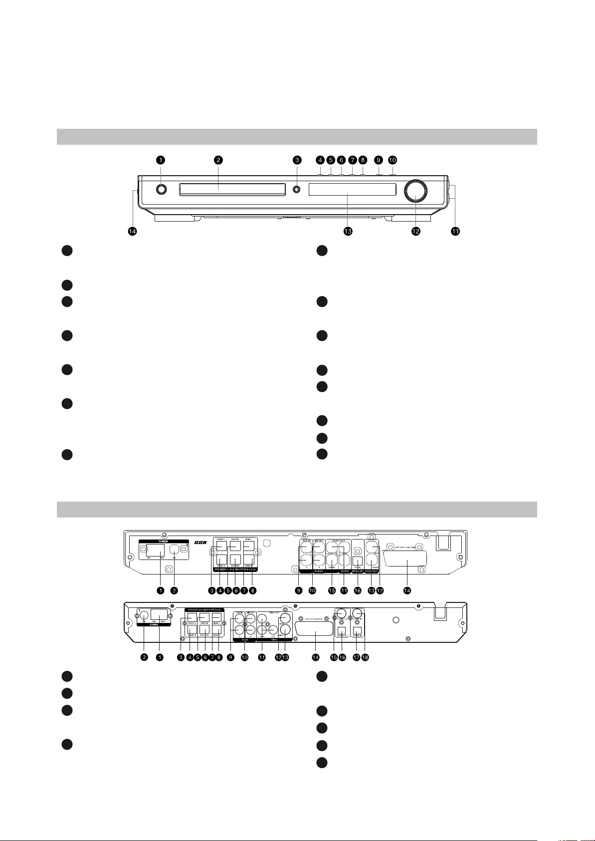
2.2.1 Front panel controls
1
STANDBY/POWER button
Press to switch the device on/into standby.
2
Disc tray
3
OPEN/CLOSE button
Press to open/close the disc tray.
4
PREV button
Press to playback from the previous bookmark
5
NEXT button
Pres to playback from the next bookmark
6
REW button
Press to playback fast reverse/radio station
tuning
7
Button
FWD
Press to playback fast reverse/radio station
tuning
2.2.2 Rear panel connections
8
SOURCE button
Press to switch between DVD-receiver/Audio
input/Tuner/Digital audio input.
9
PLAY/PAUSE button
Press to playback/pause
10
STOP button
Press to stop the playback
11
Microphone input
12
VOLUME adjuster
Press to adjust volume.
13
VFD display window
14
Headphones input
15
USB port
1
AM Antenna input
2
FM Antenna input
3
Left front speaker input (output from the build in
amplifier)
4
Right front speaker input (output from the build-in
amplifier)
- 5 -
8
Right Surround speaker input (output from the
build-in amplifier)
9
Audio input
10
Stereophonic audio output
11
Component video output Y Cb (Pb) Cr (Pr)
Composite video output
12
Page 10
Center speaker input (output form the build-in
5
amplifier)
6
Subwoofer input (output from the build-in
amplifier)
7
Left Surround speaker input (output from the
build-in amplifier)
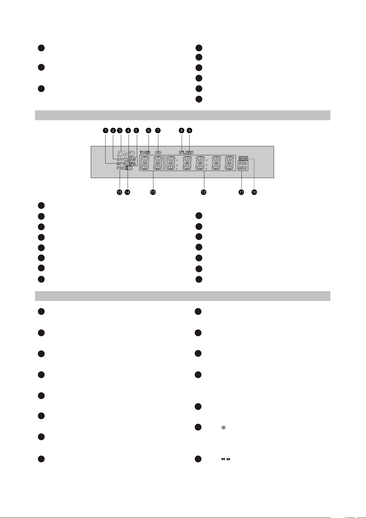
2.2.3 VFD display general view
1
MP3-disc
2
CD-, VCD-or SVCD-disc
3
DVD-disc
4
Repeat
5
AM/FM
6
Radio tuning mode
7
Tuner tuning mode
8
Stereo
S-Video output
13
14
SCART-type AV connector
15
Coaxial digital audio output
16
Optical digital audio output
17
Optical digital audio input
18
Coaxial digital audio input
9
Dolby Digital
10
Programmed radio station
11
Friquency
12
Playback time
13
Chapters or tracks
14
Playback or pause
15
PBC
2.2.4 Remote control general view
1
EJECT button
Press to open/close the disc tray.
2
DVD button
Press to switch to DVD mode
3
AUDIO button
Press t switch to audio input mode
4
DISP button
Press to display the disc information
5
LANG button
Press to change the canuage
6
SLEEP button
Press to turn the sleep mode on
7
Q-PLAY button
Press to tum the Q-play mode on
8
EQ button
Press to adjust the equalizer
9
BASS+/- button
Press to adjust subwoofer
10
BOOST button
Press to bass boosting
11
BROWSER button
Press to turn on/off browser function
12
JOG DIAL wheel
Functions are set manually. Default function:
zoom
13
SETUP button
Press to switch to setup mode.
14
Button
Press to capture and bookmark image for the
wallpaper
15
Button
Press to start reverse or forward scanning
- 6 -
Page 11
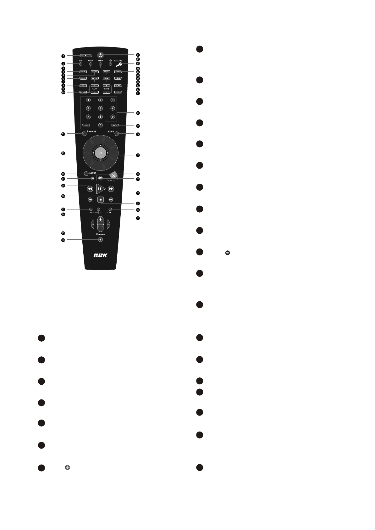
SKIP/RESET +/-
16
Press to switch between files on disc/tuned radio
stations
17
A-B buttons
Press to repeat the selected portion
18
REPEAT button
Press to repeat playback
19
CH+/CH- button
Press to change the acoustic channel
20
MUTE button
Press to change the acoustic channel
21
VOLUME+/- button
Press to adjust the volume
22
SLOW button
Press to switch to slow down the playback
23
PLAY/PAUSE button
Press to play/pause the playback
24
STOP button
stopped/playback from the previously meorized
point.
35
HDMI button
Press to switch to HDMI mode.
36
SUBT button
Press to change the subtitles language
37
ANGLE button
Press to change the camera angel
38
RADIO button
Press to switch to radio mode
39
KARAOKE button
Press to set the karaoke functions
40
USB button
Press to switch to USB mode
Button
41
Press to switch the device on/into standby
Press to stop the playback
25
Button
Press to turn on/off the virtual control panel
26
CANCEL button
Press to go one level back/cancel current
operation
27
OK button
Press OK for confirmation of use it like joystick
during navigating in MENU
28
MENU button
DVD-disc menu/PBC function
29
GOTO button
Press to playback from the target place
30
Numeric buttons
31
ST/5.1 button
Press to switch between STEREO/5.11CH
32
TREBLE +/- button
Press to adjust the tone
33
ECHO button
Press to adjust the echo function of the
microphone
MEM button
34
Press to memorize the point where playback was
- 7 -
Page 12
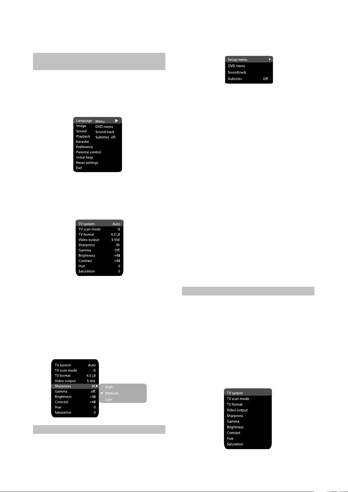
2.3 FUNCTION SETTINGS
2.3.1 Function selection and
change
Press the SETUP key to show the setup
menu. You will see the following image on the
screen, as shown on the figure: Select the
desired menu item using the jog Dial; Press OK
confirmation.
1.For example, if you wish to change the image
sellings, you have to select the lmage item and
press the OK or GIGHT key of the cursor
joystick.
2.Using the jog Dial, select the desired item and
press OK or RIGHT key of the cursor joystick.
Fox example, select the Sharpness item.
Settings will appear on the screen. Then select
the desired sharpness level and press OK for
confirmation.
3.Press LEFT key of the cursor joystick for exit to
previous menu level.
4.Press SETUP to exit setup menu.
# Default option: English
2.DVD-menu: Selection of disc menu language.
3.Soundtrack selection of translation language
#
Options: Russian, English, Estonian,
Lithuanian, Kazakh, Romanian, Belarusian,
Ukrainian, Chinese.
#
Default: English.
#
Selection of other languages: Select the
OTHERS item using the jog Dial and press OK.
Enter the language code using the number
buttons and press OK.
#
If the language you select is not recorded on
the DVD disc, another available language will
be used.
4.Subtitles: Selection of subtitles language
#
Options: Off, Urssian, English, Estonian,
Lithuanian, Kazakh, Romanian, Ukrainian and
Chinese.
#
Default option: Off.
#
Selection of other languages: Select the
OTHERS item using the jog Dial and press OK.
Enter the language code using numeric
buttons and press OK.
#
If the language you selected is not relcoded on
the DVD disc, another available language will
be displayed.
2.3.3 Image settings menu
1.TV system: TV system selection.
#
Options:Auto, PAL, NTSC.
#
Default option Auto.
2.TV scan mode: scan mode selection
#
Options: Progressive, interlaced.
#
Default option: interlaced
#
Progressive scan is transferred only via a
component video output.
#
Before switching to progressive scan, make
sure that your TV set supports this operation
mode.
2.3.2 Language settings
1.Menu: interface language setup
Options: Russian, English, Ukrainian.#
- 8 -
Page 13
3.TV Format: image ratio settings
#
Options: 4:3 pan&scan, 4:3 letterbox and 16:9
TV.
#
Default option: 4:3 pan & scan.
#
some discs are recorded with support of only
one ratio. The selected radio must comply with
the TV screen.
4.Video output: selection of video signal.
#
Options: S-Video, Comp, RGB
#
Default option: Comp.
6.Gamma: adjustment of image color
temperature.
#
Options: High, Medium, Low, Off.
#
Default option: Off.
7.Brightness: adjustment of image brightness.
8.Contrast adjustment of image contrast.
9.Hues: adjustment of image hues.
10.Saturation: adjustment of image saturation.
Adjustment of image brightness; contrast, hues
and saturation.
#
Select the desired item of the image
adjustment section using the jog Dial. Press
OK or RIGHT key to start adjustong the
relevant option.
#
Change the option value using the jog Dial.
#
Upon completion press the LEFT of the cursor
joystick to return to image setup menu.
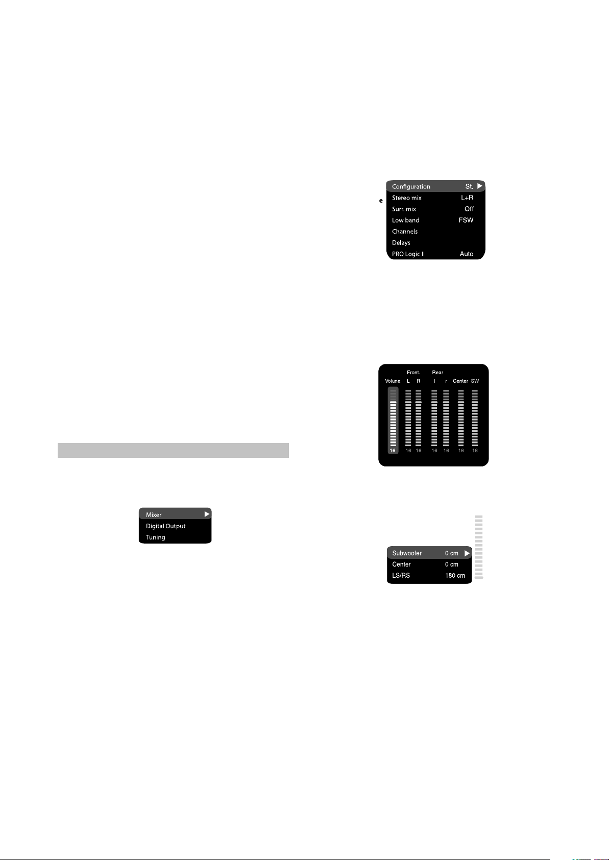
2.3.4 Sound settings menu
1.Mixer
a) Configuration: setting of the mode for
conversion of the 5-channel signal.
Options: Front F, Center C, Surround Sr,
#
Subwoofer SW.
Default options: Front F, Subwoofer SW.
#
If you want the low-frequency component of
#
the sound signal enter only the subwoofer
channel, select and confirm the parameter
Subwoofer SW.
e) Channel settings: separate adjusting of
volume by channels.
Select the channel you want.
#
Adjust the sound volume of each channel using
#
the wheel.
Press the OK to return to sound settings menu.
#
f) Delay of the channel: Set-up of signal delay in
speaker channels(central, rear and subwoofer)
Options: Stereo, 5.1.
#
Default option: Stereo
#
5.1 mode must be supported by the disc.
#
Number of music accompaniment channels
depends on the specific disc.
Adjustment of the central speaker and
#
surround speakers is available only if the
Configuration option is set to 5.1 position.
b) Stereo mix: playback set-up while playing the
disc with two independent audio channels.
Options: L+R, L, R.
Default options: L+R.
#
c) Surr.mix: set-up of surround oftions while
playing the sereo disc.
Options: Off, Sum, L+R, Virt, Surr.
#
d) Low band: distribution of low frequencies
through channels.
#
Using the jog Dial, select the channel, for
#
which you want to set up the delay and press
OK for confirmation.
Using the jog Dial set up the desired distance
#
from the listener to each speaker(dectiled
description of this operation see on page 32)
g) PRO Logic ll: function of stereo sound
conversion to 5-channel sound.
Options: On, Off, Auto.
#
Default option: Audio.
#
In Auto position, the DVD receiver determines
#
itself, when to use the PRO Logic ll decoder.
Some discs do not support this function.
2.Digital audio output.
- 9 -
Page 14
a) SPDIF format: set-up of digital audio output
options.
#
Options: RAW, PCM
#
When you select the RAW option, the not
decoded signal is sransferred to the DVD
receivers digital outputs, the decode signal is
transferred to analog outputs. Decoding is
performed by the built-in decoder of the DVD
receiver. This feature is meant to ensure that
signal decoding at digital outputs is performed
by an external device(e.g.an amplifier)
#
If you select the PCM option, a PCM coded
signal will be transferred to the DVD receivers
digital outputs.
b) LPCM: Set-up of digital audio output options
to comply with different amplifiers and
receivers.
#
Options: 48 kHz 16 bit, 96kHz 24 bit.
#
Defacelt option: 48kHz 16bit.
3.Sound correction
a) Max volume: max volume limiting.
#
Using the jog Dial, adjust the max volume level.
#
Press the LEFT key of the cursor joystick to
return to sound correction setup menu.
b) Equalizer: equalizer modes.
#
Options: Rock, Pop, Live, Dance, Techno,
Classic, Soft.
#
Default option: Off.
c) Echo: echo effects
#
Options: Off, Concert, Living room, Hall,
Bathroom, Cave, Arena, Church.
#
Default option: Off.
d) Tone balance: adjustment of tone balance
level.
#
Adjust the tone balance level using the jog Dial.
#
Press the LEFT key of the cursor joystick to
return to sound correction setup menu.
2.3.5 Playback settings
1.DVD
Advertisment skip: skip the unskippable
block while playing a DVD disc.
#
Options: Yes, number
#
Edfault option: number
If on option is set, while reproducing discs, a
#
menu will appear, in which you can select the
or order of playing the disc content. If the off
option is wet, the reproducing of content is
performed is the order, in which it is recorded
of the disc.
3.Flids” Selection of reproduced files on the disc.
Options: Audio, Pictures, Video, All types.
#
Default option: All types.
#
4.Repeat: file repeat mode.
Options: Off, Single, All
#
Default option: Off.
#
5.Load effect: type of transition from one JPEG
file to another.
Options: Off, from top, from bottom.
#
Default option: Off.
#
2.3.6 Karaoke settings menu.
1.Microphone: MICROPHONE ON/OFF.
Options: On, Off.
#
Default option: Off.
#
2.Kar. Help: karaoke-disc playback mode
Options: L channel, R Channel, No ast, NO vol.
#
Default option: No vocal mode.
#
3.Volume:
Microphone: microphone sound volume level.
Using the jog Dial adjust the microphone
#
volume level.
Press LEFT key to the cursor joystick to return
#
to karaoke settings menu.
4.Echo: echo level while playing the karaoke-
disc.
Adjust the echo level Using the jog Dial.
#
Press LEFT key of the cursor joystick to return
#
to karaoke settings menu.
2.VCD/SVCD
PBS menu: PBC menu on/off
Options: On, Off.
#
Default option: On.
#
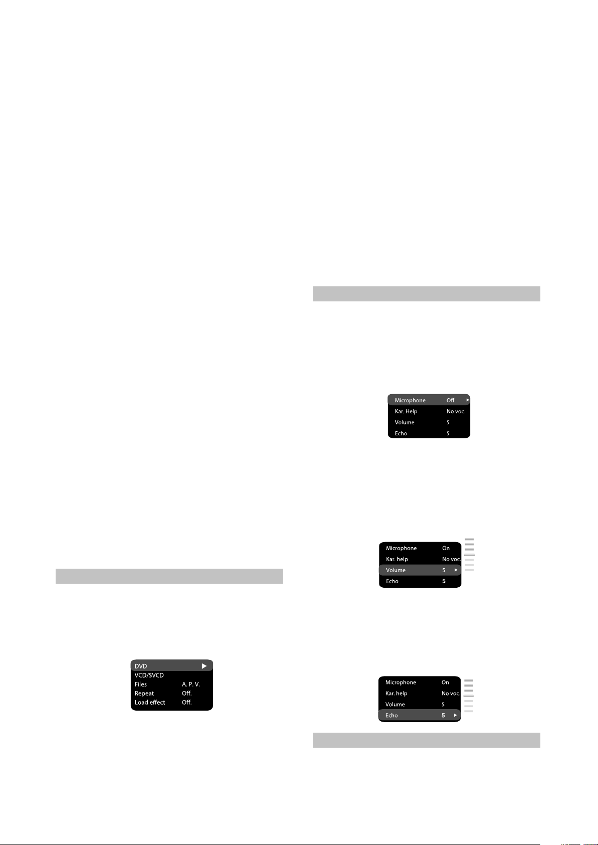
2.3.7 Preference settings
1.Gr.Equalizer: Spectrum analyzer.
Options: On, Off.#
- 10 -
Page 15
# Default option: Off.
#
Default option: Off.
2.Background: selection of an image as TV
screen wallpaper.
#
Options: Standard, Saved
Default option: Standard.
#
3.Screen saver: Screen saver on/off.
Options: On, Off.
#
Default optioon: On.
#
4.Jog Dial
Options: Zoom, Step, Skip, Volume.
#
Default: Zoom.
#
2.3.10 Reset to defaults
Resetting all settings and restoring default
options, except age restrictions level and
password.
2.3.11 Exit settings menu
Select the item using the jog Dial and press the
#
OK to exit the menu.
2.3.8 Parental control
1.Category: Setup of age restrictions to prevent
children from seeing undesirable discs.
Options: Any, Kid, G, PG, PG-B, PGR, R, NC-
#
17
Default option: Any.
#
2.Set password: Setup of a four-digit password
to change the level of age restrictions.
Default option: 7890.#
2.3.9 Initial setup menu
#
Press the RIGHT key of the cursor joystick to
enter the initial setup menu, then select the
desired item using the jog Dial and press OK
key for confirmation.
#
While being in this menu section, you cannot
return to the previous level by pressing the
LEFT key of the cursor joystick.
2.3.12 Channel delay set-up
Set-up of tine delay in the surround
channel
Usually, time delay in the Dolby Digital
decoding system is preset to ensure best offect
while installing the Hone Theater. However, in
case y you with to adjust your system more
precisely, please consult instructions given in
this manual. Set up of time delay for this device
is possible in both Dolby Digital and Dolby Pro
Logic modes.
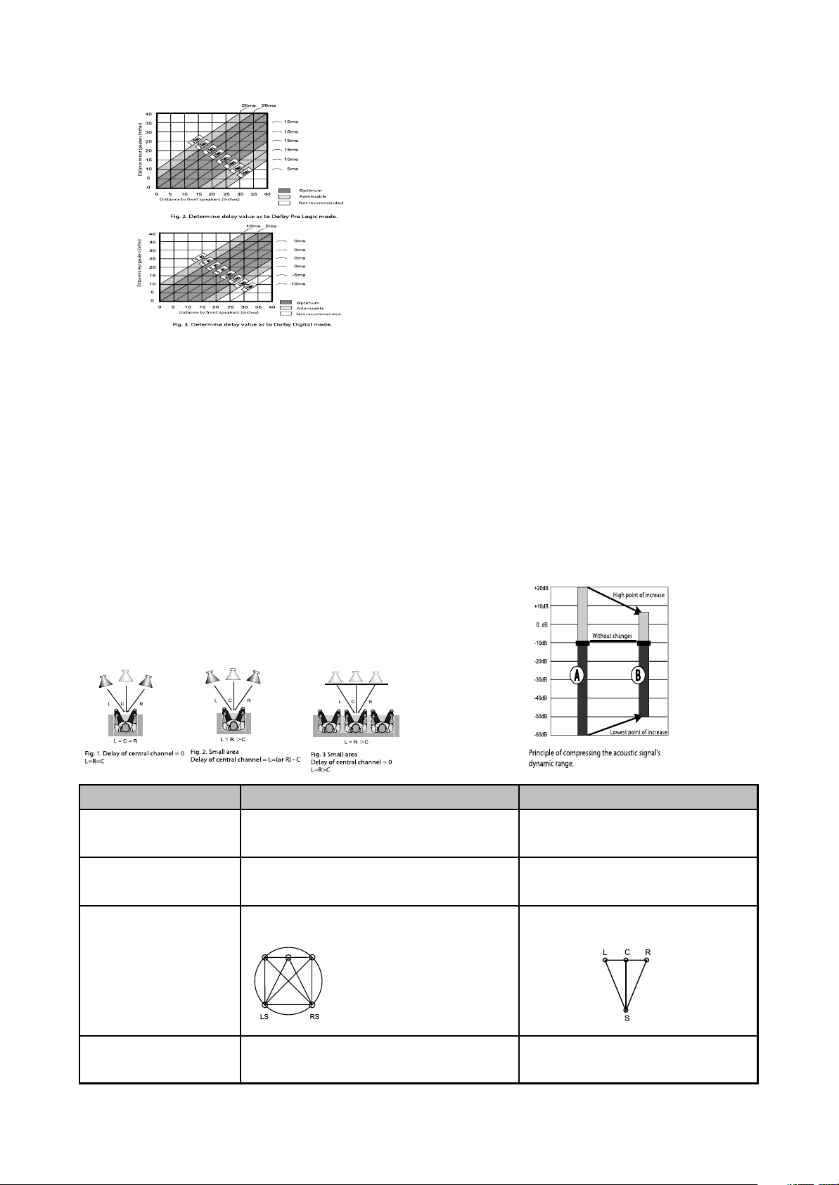
Fig.1.Take into account the
A-B distance; use both
figures for setting the
desired time delay.
To set the desired delay you have to know
the distance from the place where you are to the
front speakers and surround speakers as shown
in Fig.1: Consult Fig.2(Dolby Por Logic mode)
and 3(Dolby Digital mode) in order to determine
the distance to Surround Speakers(axis Y in the
figure) and the distance to the front
speakers(axis X in the figure). Crossing point of
those tow Lines on the chart will give the
recommended delay value.
- 11 -
Page 16
Set-up of time delay in the central
Dolby Digital Dolby Por Logic surround
Rear channel Stereo 20 Hz-20kHz
mone channel with limited
frequency range(100Hz-7khz)
Low-frequency
channel(subowwfer)
Autilable, 20-120Hz N/a
Sound field
distribution
Multivariate From left to right from right to left,
from front to rear, from rear to
front
Channels
6 independent channels, each
reproducing its own signal at a time
4 segmented channels. Only one
channel is decoded at a time.
channel
Sometimes several people are listening to
the music, and the space is limited. In this case,
you can install three speakers(two front ones
and a central one) as shown in Fig.1. With the
distance to the listener being approximately the
same. The central channel delay is to be set at
“0”.
Should the central speaker be in close
proximity to left and right front speakers as
shown in Fig.2,or the central speakers in one
line, as shown on Fig.3 with the delay value of
the central to be set at “0”.
Finally, if it will be necessary to install the central
speaker behind the left and right front speakers,
the delay value shall be set at “0”.
“Night” mode
The Dolby Digital system provides an
extremely broad dynamic range of playback
sound-from gentle to roaring. It creates the
presence effect, especially while seeing motion
pictures. However, at night a powerful sound
with a broad dynamic range may give pleasure
to you, but disturb and annoy your family and
neighbors.If you just decrease the volume, you
will immediately notice that you ceased to hear,
e.g., dialogues as clear as you do at normal
volume, and such sound effects as rustle,
whisper etc have merely disappeared. To avoid
this, you just have to decrease the volume of
“soft” sounds with the volume of “average”
sounds left unchanged, i.e. Just decrease the
dynamic range of sound accompaniment. Only
Dolby Digital system provides for such a method
of sound control. It uses the principle of
compressing the acoustic signals dynamic range
while recording; there fore; while playing an
inverse transformation(volume expansion) takes
place. This is called “night” mode. The regulation
limits are restricted; however, to avoid
distortions of resultant signal.
- 12 -
Page 17

Creates an optimum sound field with
illusion of an equal distance from
listener to each speaker
The most cost-efficient way to
ensure high-quality surround
effect
Allows adjusting the decompression
dagree of sound information("night"
mode)
Surround sound may be received
from any signal source.
Possibility of program mable control of
the decoder to transfer basses into lowfrequency channel in systems equipped
broad-band speakers and a subwoofer
Compatible with existing and
future two-channel(stereo)
formats
Undoubted progress in sound recording
technology, especially important for
program directors, film directors, sound
engineers and actors
Big progress in comparison whti
conventional stereo, the worol's
mosst popular surround format.
Miscellaneous
- 13 -
Page 18

Chapter Three Principle and Servicing
Section One Principle of the Player
3.1.1 Function introduction
This players adopts new-generation DVD decode chip with built-in Dolby decoder, and the vivid
surround system brings you to taste the living cinema effect. It has the following features:
Progressive scanning output to produce steadier and clearer pictures without flickering
Composite video, S-video and component video output
Digital picture adjustment to sharpness, brightness, contrast, chroma and saturation of pictures,
gamma correction
Built-in Dolby digital decoder
Hi-FI stereo headphone output
FM/AM digital tuning function, capable of storing (memorizing) 20 FM/AM radio stations
respectively
Compatible with DIVX, MPEG4 format movie
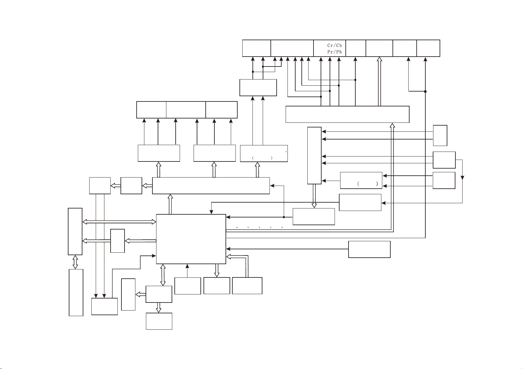
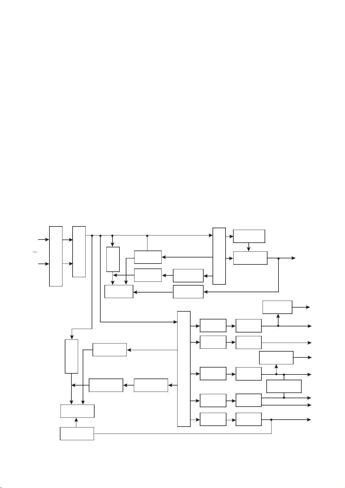
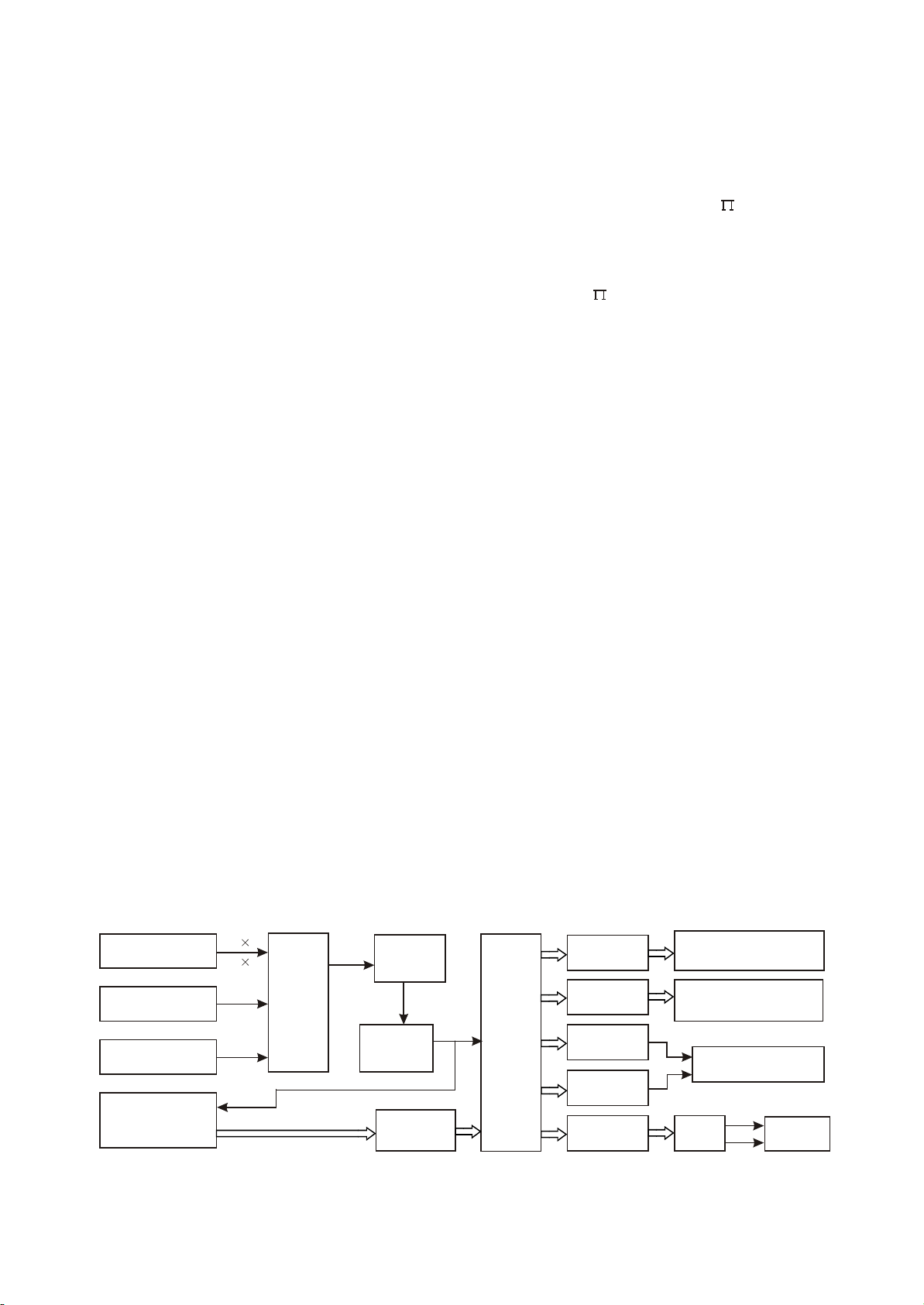
3.1.2 Block diagram principle of the player
The player is composed of decode & servo board, power amplifier board, input/output board, panel,
headphone board, tuner, power board and loader. Shown in the figure 3.1.2.1, except that power board
is not shown, other signal flow is basically shown in the figure. The main function of loader is to read disc
information and send to MT1389, MT1389 finishes servo function through D5954 on decode board and
other supplementary circuit, other circuits are used to guarantee the normal working of loader. FLASH
on decode board is to store system program, SDRAM is to store program and information of sound and
picture read from disc when the machine is working and guarantee their normal output. The main
function of power amplifier board is to perform audio DA conversion and amplification of analog signal to
output 5.1CH to guarantee the normal working of external speaker. The main function of AV board is to
output various audio and video signals. This player is attached with headphone and microphone to meet
requirements from customers. In addition, there is external sound input, and you may use the power
amplifier board of this player to perform power amplifying to it to facilitate to output to speaker. The tuner
of this player also makes it have tuning function, and it also equipped with SAA6558 chip, so it may
realize RDS function of Europe and RBDS function of US.
- 14 -
Page 19
ROUTX
L R
LOUTX
SCART
Y
Video S-video
VIDEO COMP
Optial
VEDIOC VIDEOY
Coaxial
Filtering
VY
Front
Rear
Rear
L R
SLOUT
Figure 3.1.2.1 Block diagram of the player
Woofer
SROUT
Center
SW+ SW-
CEN
Front
L
R
FROUT
FLOUT
CD4052
N13
TAS5112
- 15 N11
RC4580
HR
HL
N10
RC4580
SCL
SDA
SCLK
LRCK
N12 TAS5508
SDAT A0
SDATA1
SDATA2
N14
TAS51 12
DAVNIN
XS301
D5954
U201
MT1389
Amplifying circuit N8
N9 TLV272
SDA AD
ADC DAT
CS5340
Y1 Y2 Y3 Y4 Y5 Y6
SPDIF
URST#
VV
VU
Filtering
AUXR
AUXL
TUL
TUR
Amplifying circuit
OK
SAA6558
M 4558
N6
Reset circuit
MIC 1
MIC 2
PDS MPX
L
External
audio input
R
Tuner
Microphone
HDET
Loader
Headphone
VFD
Screen
CLK
STB
SDA
N102
SO793
Button
IR
N103
REMOT
IR receiver
U207
FLASH
U208
SDRAM
Page 20
Section Two Unit Circuit Principle
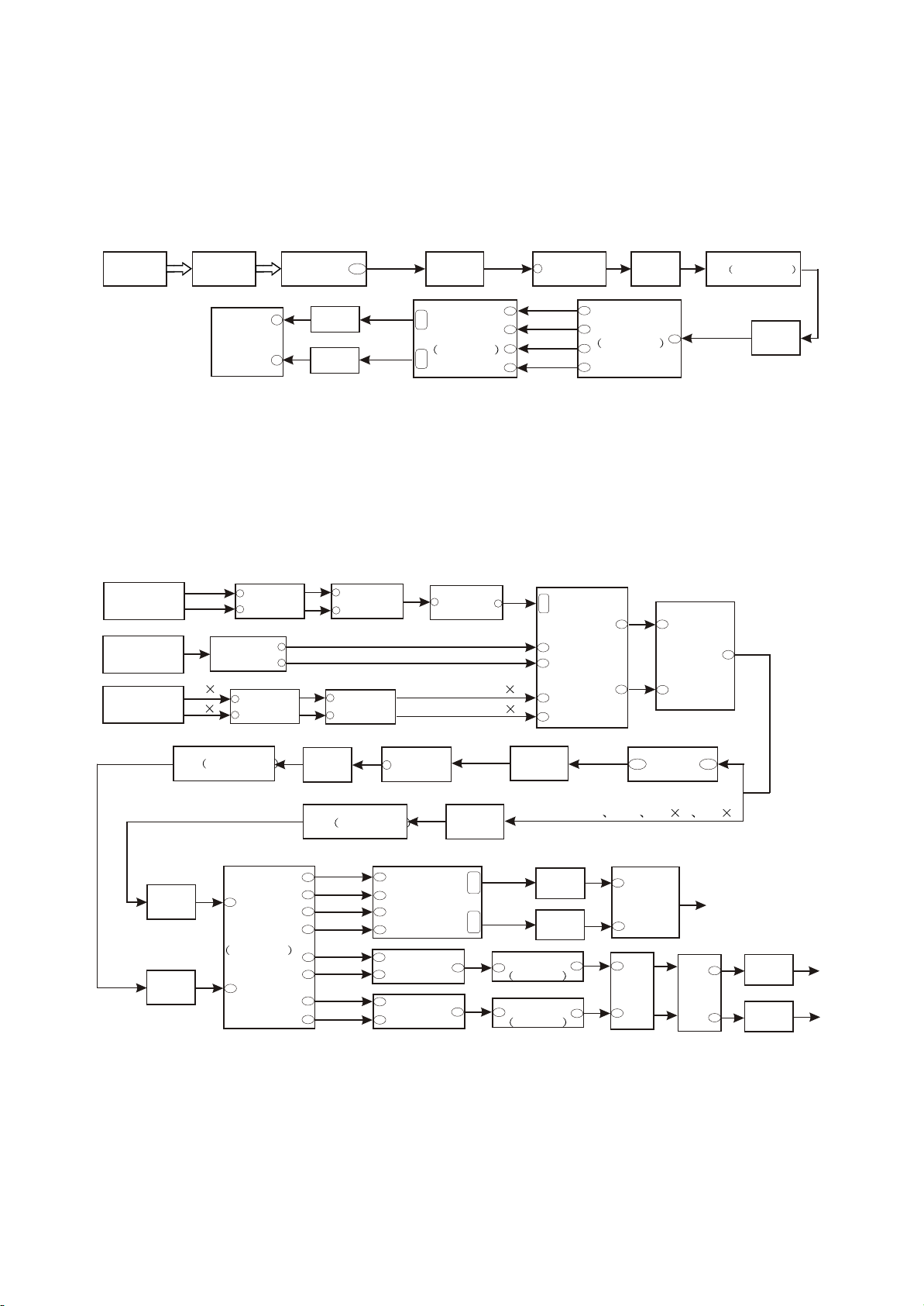
3.2.1 Decode circuit
1. Decode circuit block diagram is shown as in the following figure 3.2.1.1:
SDCLK
SDCKE
DCS
DRAS
SWE
SDRAM
DQM0
DQM1
DQ0~DQ15
MA0~MA11
FLASH
PWR
PRD
PCE
A0~A20
AD0~AD7
URST
Reset
circuit
MT 1389
SDA
SCL
EEPROM
24C02
Figure 3.2.1.1 Decode circuit block diagram
Clock
27M
V18
1.8V
voltage
regulating
U206
2. Working principle: this decode circuit is mainly composed of MT1389, SDRAM and FLASH.
Working condition of decode circuit has:
(1) Reset: refer to reset circuit working principle for details.
(2) Clock: this system adopts 27M external clock input, and produces clock signal required by
system inside through internal frequency doubling circuit.
(3) Power: decode chip adopts twp groups power supply of 3.3V and 1.8V, in which 1.8V mainly
supply power for internal logic control circuit and we call it core voltage.
After power on, reset circuit performs reset to MT1389 built-in CPU (8032) and FLASH, decode chip
outputs reset signal at the same time and performs reset to other circuit. After system reset, it firstly
sends out read signal to FLASH to read out in formation saved in FLASH, the machine displays power-
on picture, servo system begins to work to check whether machine closes door to proper position and
- 16 -
Page 21
Whether detect switch has been closed, if not, the door close action is performed. After detect switch of
door is closed, the machine begins to perform preparations of disc reading and performs panel display
at the same time of working.
Playback process: laser head picks up disc signal from disc, after servo system processing, then
send to decode circuit for decoding, signal after being decoded is saved in SDRAM for the moment.
When machine needs to replay signal, decode circuit calls information inside SDRAM to perform D/A
conversion and then output.
User information storage: information content set by user is saved inside EEPROM, if user does not
refresh or reset this information, it will saved in IC permanently.
Audio, video output circuit: at present, MT1389 all integrates video D/A converter, MT1389E inside
integrates audio D/A converter, manufactures select according to their own needs. Please refer to
circuit principle diagram and audio circuit explanation for details.
3.2.2 Servo circuit
Servo system of this player adopts SANYO loader MTK decode solution (MT1389E+FLASH
(16M)+SDRAM (6
4M)), and its servo circuit is mainly composed of front stage signal processing and
digital servo processing, digital signal processing IC MT1389E and drive circuit D5954, in which
MT1389E is also the main composition of decode circuit at the same time, shown in the figure 3.2.2.1:
IOA
MD11
LDO2
LDO2
MT1389
XS101
Feed
electric
machine
Main axis
electric
machine
Main axis
control detect
circuit
Switch circuit
APC circuit
A B C D E F RFO
TK-
15
TK+
16
FC+
14
FC-
13
SL+
17
SL-
18
SP-
12
SP+
11
D5954
23
26
FOSO
1
FMSO
TRSO
DMSO
6
Open/close
circuit
Figure 3.2.2.1 Servo circuit block diagram
- 17 -
Page 22

2. Working principle:
After powering on or closing to proper position (on loader frame for general DVD player, on PCB
board of below part of card door for PDVD player), loader lens begins to reset; after laser head is on
proper position, detect switch will give a signal to MT1389, MT1389 begins to output focus, main axis
and light emission signals, disc begins to rotate, laser head begins to recognise disc information, and
judges whether disc is CD or DVD according to disc information to facilitate to output level from IOA pin
to control disc switch circuit and laser head PDIC to make the corresponding control acts. At the same
time, Mt1389 adjusts laser output power through laser power control circuit.
After loader reading disc information, through photoelectric conversion, A, B, C, D, E, F signals are
formed to give to MT1389 (DVD only has A, B, C, D signals), and then inputted from pin 2~11, 18, 19 of
MT1389. After being amplified and processed by the pre-amplifier inside MT1389, now signals are
separated to two part s for processing inside MT1389. After being added amplifying and through
subtraction circuit, one part of signals produce servo error signals and form the corresponding servo
control signal after being processed by digital servo signal circuit and output FOO, TRO, DMO, FMO
servo control signals from pin 42, pin 41, pin 37, pin 38 of MT1389 respectively, through the integration
circuit composed by resistor and capacitor, FOSO, TRSO, DMSO, FMSO signals are sent to servo drive
circuit for amplifying and then brings along fucus coil, trace col, main axis electric machine and feed
electric machine after drive amplifying. Among these, focus and trace servo are used to correct objective
position accurately; feed servo is used to bring along laser head to make radial large-scale move which
belongs to the preliminary adjustment to pick-up position; and main axis servo is used to control main
axis electric machine to make it read signals in means of constant linear velocity and bring along disc to
rotate. After processing of amplification by VGA voltage control amplifier and equalization frequency
compensation inside MT1389, another part of signals are changed into digital signals through internal
A/D converter. When loader is reading CD/VCD signals, these signals are conducted EFM demodulation
inside MT1389, and then outputted to latter stage for AV decoding after finishing CIRC (Cross-
Interleaved Reed-Solomon Code) error correction inside. When loader is reading DVD signals, these
signals are conducted ESM demodulation inside MT1389, and then sent to latter stage for decoding
after finishing RSPC error correction inside. General DVD player has a open/close circuit, which controls
the in/out action of door to reach the purpose of conveying discs. PDVD player adopts manual means to
open the door, and you may judge whether door closes to proper position through detect switch.
3. Explanation to servo terms
(1) FOO: because of the error in disc make, when rotating, disc may probably move upwards or
downwards slightly to make the focus of laser emitted by pick-up cannot justly fall on data pit of disc, so
pick-up is required to move upwards or downwards to make focus aim at data pit justly. The main act is
to make object lens move upwards and downwards.
(2) TRO: data information is saved in disc in form of tracks. When disc is rotating, there will be track
- 18 -
Page 23
Deviation, now laser head is required to adjust. In this process, the object lens moves forwards or
Backwards, and the moving range is very small.
(3) FMO: similar to acts of trace, the acts of feed are larger than those of trace. Feed conducts a
large scale movement firstly, and then trace moves slightly in this range. Feed moves for a while, and
does not move for another while; but trace moves all the time. Feed is rough adjustment and trace is fine.
The acts are obvious when opening and selecting track.
(4) DMO: it is the performance agency for main axis disc rotation. Its rotation speed decides that of
disc. Its rotation is generated by an individual DC electric machine, in which rotation speed of DVD is
twice over that of CD.
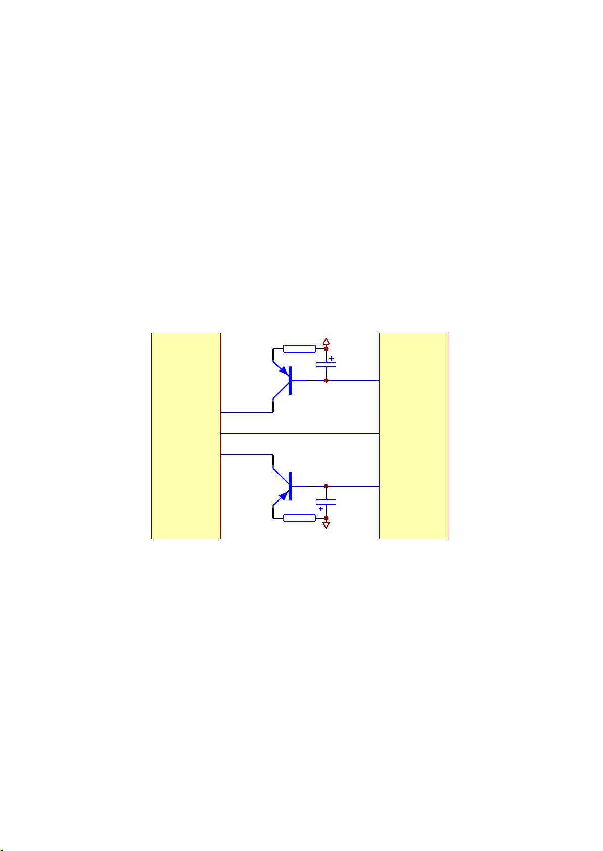
3.2.3 Laser power control circuit
1. Laser power control circuit is shown as in the following figure 3.2.3.1:
LDO-AV33
R301
4.7R
TC302
47uF/16V
LDO2
23
Q301
2SB1132-S
XS301
20
19
MD1
Q302
2SB1132-S
20/21
MT1389E
LDO1
TC303
47uF/16V
4.7R
R302
Figure 3.2.3.1 Laser power control circuit diagram
2. Working principle
Pin 20/21 of MT1389 is laser power detect signal input pin, pin 21 is DVD laser power strong/weak
detect signal input pin, pin 23 is VCD laser power drive control output pin, pin 22 is DVD laser power
drive control output pin.
When reading VCD disc, laser power becomes weak, voltage of MDII pin decreases, voltage
LDO-AV33
decrease of pin 23 of MT1389 makes voltage of pin 19 of XS301 increase to reach the purpose of raising
laser power. When laser power is too strong, voltage of MDII pin increases to lead to voltage of pin 23 of
MT1389 increase to make voltage of pin 19 of XS301 decrease to reach the purpose of reducing laser
power to form an auto power control circuit.
- 19 -
Page 24
Name
When reading
disc normally
When disc out When disc in
When no
disc in
TROPEN 0
There is about 1 second 3.3V
pulse when at the moment of disc
out
0 0
TRCLOSE 0 0V
There is about 1 second 3.3V pulse
when at the moment of disc out
0
TROUT 3.41V
3.3V 0V 0V 3.3V
3.3V
TRIN 0
0V 3.3V 3.3V 0V
0
OPO 2.61V 2.75V 2.64V 2.61V
ADIN 2.61V 2.76V 2.61V 2.61V
OP+ 1.66V 1.81V 1.27V 1.81V
OP- 1.85V 2.12V 1.47V 2.04V
When reading DVD disc, pin 21 is detect signal input pin, pin 22 is drive control input pin, and the
working principle is the same with that when playing VCD disc.
3. Key point voltage (unit: V) is shown as the following table:
3.2.4 Main axis control circuit
1. Main axis control circuit is shown as in the following figure 3.2.4.1:
SP-
SPL-
2. Function: disc is always in high speed rotation in the course of disc reading, when you need to
open the door to change disc, MT1389 stops the positive direction drive signal which is given to main
axis drive circuit, for the function of inertia disc is still rotating. If disc out order is performed at this time,
disc will be abrasively damaged. Therefore, machine must be baking to main axis, that whether disc has
stopped rotating and whether disc is reversing, decode chip of the machine cannot recognize. So a main
C307 222
OPO
R320
150K
R317 680K
R318
0R
ADIN
OP-
R321
1R
R319
C308 222
OP+
V1P4
150K
R322 680K
Figure 3.2.4.1 Main axis control circuit diagram
MT1389
axis control circuit is added to make decode chip can effective monitor that whether disc has stopped
rotating.
- 20 -
Page 25
Key point Position Voltage Remark
DV33 (point A) Diode VD201 cathode 3.3V
TC217 may sends out current from this
point after power failure
Point B Diode VD201 anode
3.3V after reset
finishes
After reset finishes, voltage increases from
0V to 3.3V
Point C Pin 5 of reverter 0V after reset finishes
After reset finishes, voltage decreases from
3.3V to 0V
URST# (point D)
Connection place of
R256 and R253
3.3V after reset
finishes
After reset finishes, voltage increases from
0V to 3.3V
3. Working principle: MT1389 has a comparator inside composed of operational amplifier, in which
OP+ is the in-phase input end of operational amplifier, OP- is reverse input end, OPO is output end,
when playing disc normally, for electric machine is positive direction rotating, voltage of OP+ is higher
than that of OP-, voltage of OPO is more than 1.4V. When disc out is needed, main axis drive signal
stops, for electric machine is permanent magnetic, when in rotating, induced electromotive force
produces in two ends to give to decode chip through R320, R319 sampling to make OPO output less
than 1.4V voltage and transmit to input pin of MT1389 ADIN through R318. When ADIN is high level,
main axis drive output end has not any drive signal output, when ADIN is low level, MT1389 outputs a
reversing drive signal to main axis drive circuit to make main axis electric machine speed down. Thus
circular working goes on until main axis stops rotating. PDVD is manual disc out means, so after disc out,
disc is still rotating, but will stop very son.
4. Key point voltage (unit: V) is shown as the following table:
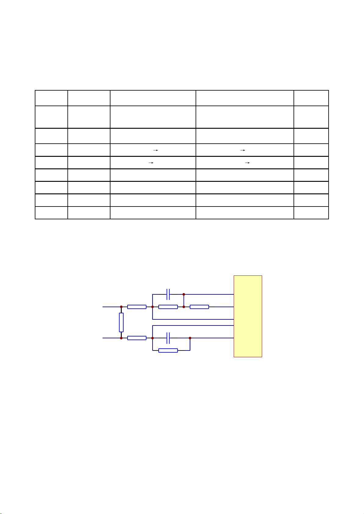
3.2.5 Control panel circuit
1. Control panel circuit block diagram is shown in the following figure 3.2.5.1:
FL+
FL-
D+5V
-21V
XS 201
DGND
LED1
LED2
Volume
knob
J4
J3
Figure 3.2.5.1 Control panel circuit block diagram
VFD screen
Grid1~Grid8
Seg2~Seg16
S0793
DATA
X S401
- 21 -
STB
CLOCK
Seg2
Seg3
Seg4
Seg5
KEY2
KEY1
Remote control
receiver
IR
Button
Page 26
2. Working principle
(1) Realization of button function: when users are operating machine, button matrix circuit will
produce a button information, and recognise button through S0793 to produce button function code to
transmit to the main CPU inside decode chip, CPU performs the corresponding switch to the function
module inside system, and a signal will produce to control OSD and panel display part to make the
corresponding display.
(2) Panel display drive: when the serial data signals conveyed by decode chip is transmitting to
panel IC (S0793), IC performs VFD drive according to the information conveyed by decode and displays
the corresponding content (controlled by software).
(3) Panel light control light: LED2 controls power switch indicator light, and it is high level after
power on; LED1 controls open/close button indicator light, after power on, low level is outputted to
lighten VD105, square wave signal is outputted when disc out and disc reading, VD105 flashes, it is high
level when playing normally, VD105 turns out.
3.2.6 Power circuit
1. Power circuit block diagram is shown in the following figure 3.2.6.1:
filtering circuit
Electromagnetic interference
filtering circuit
Bridge rectification
Transformer
circuit
Switch
module
Absorption
loop
Filtering
Start-up
Absorption
loop
Filtering
Rectification
diode
Feedback
loop
Rectification
circuit
Rectification
circuit
Transformer
Rectification
circuit
Rectification
diode
Rectification
circuit
Rectification
circuit
220V
circuit
Start-up
Switch module
Rectification
diode
Filtering circuit
Filtering
circuit
Filtering
circuit
Filtering
circuit
Filtering
circuit
Filtering
circuit
P+28V
5V voltage
regulator
Voltage
regulating diode
Voltage
regulating diode
A+5V
A+12V
D+5V
A-12V
-21V
FL+
FL-
D+3V3
Feedback circuit
Figure 3.2.6.1 Power circuit block diagram
- 22 -
Page 27

2. Working principle: this power circuit is composed of two parts, which use the common
electromagnetic interference filtering circuit and bridge rectification circuit and filtering circuit. The first
part circuit produces P+28V DC used to supply power for power amplifier circuit; the other part is
responsible for the power supply of other module circuit of the player. The working principle of each
composed part is shown as follows:
(1) Electromagnetic interference filtering circuit: various electromagnetic radiation exists in the
surrounding environment, so it will affect the inputted AC, and the function of electromagnetic
interference filtering circuit is to filter these interference to make those that enter bridge rectification
circuit is pure 220V AC.
(2) Bridge rectification and filtering circuit: the function of this circuit is to produce a 310V DC used
for rear stage.
(3)Start-up circuit: when power on, transformer does not begin to work, now the start-up circuit
provides switch module with a power supply voltage to make it work, after transformer begins to work
normally, the voltage provided for switch module by power supply circuit maintains the working of switch
module.
(4)Absorption loop:the switch module performs on/off action in a high frequency, so a strong self-
inductance voltage will produce in transformer primary coil and switch module will probably be damaged.
The function of absorption loop is to form a loop for this self inductance to ensure the normal working of
circuit.
(5) Switch module: that inputted from transformer is 310V DC. To make transformer work, AC shape
voltage must be presented. The function of switch module is to control this 310V DC to make it on for a
while and then off for a while to produce a high/low voltage change in the primary stage of transformer,
thus the transformer can work.
(6) Power supply circuit: provides a power supply voltage for switch module.
(7) Rectification diode: the voltage that outputs from transformer is pulse DC, the function of
rectification diode is to change pulse DC to DC together with the filtering circuit behind.
(8) Feedback loop: the time of “on” and “Off” in the same cycle inside switch module 5L0380R is
decided by feedback loop. Feedback loop perform sampling to +3.3V output voltage, when output
voltage is too high, through feedback loop, the space occupation ratio of pin 4 signal of 5L0380R is
changed, the “on” time decreases, and output voltage begins to decrease. When output voltage is too
low, the voltage sampled is on low side, through feedback loop, space occupation ratio of 5L0380R
increases, output voltage increases to make power board output stable voltage through the function of
feedback loop. LM431 used in this power is a 2.5V comparator, compare sampling voltage with this 2.5V
voltage, when sampling voltage is more than 2.5V (means output voltage is on high side), LM431 is on,
light emission diode in photoelectric coupler begins to emit light to make the other end of photoelectric
coupler begin to be on, the light emission is stronger, the “on” degree is large, the “on” time of switch
module 5L0380R decreases, output voltage begins to decrease. When sampling voltage is less than
- 23 -
Page 28
2.5V (means output voltage is on low side), LM431 cuts off, the “on” time of VEPR22 increases, output
voltage increases, thus power board outputs stable voltage through the auto control function of
feedback loop.
(9) Filtering circuit: the function is to produce a stable and small-ripple DC voltage. “ “-style filter is
often adopted in filtering circuit. The features of capacitor filtering are: when load resistance is high and
current is small, filtering function is obvious; for inductor filtering, when load resistance is small and
current is large, filtering function is obvious. Constitute capacitor to “ “-type filter, it may have better
filtering effect.
3. Main functions of various voltage outputted by power board:
(1) -21V: supply power for panel main chip N102.
(2) FL+¡¢FL-: supply power for filament of panel display screen.
(3) D+5V: supply power for N102, servo drive chip U302 (D5954) and open/close circuit.
(4) P+28V: supply power for audio power amplifying chip N13, N14 (TAS5112).
(5) A-12V, +12V: supply power for audio power amplifying chip N1 (F4558), N10 (RC4580), N11
(RC4580) on power amplifier board. A+12V: supply power for tuning data processing chip N6 (SAA6558)
and tuner.
(6) D+3V3: supply power for U201 (MT1389), U214 (FLASH), U211 (SDRAM) and U205 (74HCU04).
(7) A+5V (pin 5 of XP203): supply power for loader.
(8) A+5V (pin 1, 2 of XS504): supply power for power amplifier board ADC chip N7 (CS5340), and
digital audio pulse modulating chip N12 (TAS5508).
(9) A+5V (pin 4 of XS504): supply power for power amplifier board data selection chip N5 (CD4052),
and audio power amplifying chip N8, N9 (TLV272).
3.2.7 Audio power amplifying circuit
1. Audio power amplifying circuit block diagram is shown in the following figure 3.2.7.1:
External audio input
MIC signal input
External audio input
Decode board
AU R
AU L
OK
CD4052
TUL
TUR
SDATAO,ADATA1,ADATA2
N5
AINR
AINL
OK
N7
CS5340
SDA
N4
74HCT125
N3
74HCT125
SDA AD
N12
TAS5508PAG
N13
TAS5112
N14
TAS5112
N8
TLV272
N9
TLV272
4580
N10
Surround left/right channel,
subwoofer channel output
on power amplifier board
Front left/right channel,
centre channel output on
power amplifier board
Left channel LD
AV board left/right
channel output
Right channel RO
H-R
N11
H-L
4580
Headphone
output
Figure 3.2.7.1 Audio power amplifying circuit block diagram
- 24 -
Page 29

2. Working principle: the system switches DVD signal and external input signal through the control
of N3, N4 by
M0, M1. When M0, M1 is 0, 1, through the selection of DVD signal bu system, N3B, N3C,
N3D, N4A, N4B, N4C of tri state gate buffer open, N3A and N4D close, 1389 sends the digital audio
signals SDA_LR, SDA_SLSR, SDA_SCW, SCLK, LRCK to 5508 directly for formatting, and the system
clock MCLK of power amplifier board is provided by 1389 through pin 6 of XP207, after being converted
by CS5340 AD , MIC signals are directly sent inside 1389 for processing, and overlapped to left/right
channel to output together after processing; when M0, M1 is 1, 0, through the selection of external input
signal (radio set and external audio input) by the system, N3B, N3C, N3D, N4A, N4B, N4C, N3A of tri
state gate buffer close, N4D opens, after being converted by CS5340 AD , external audio signals are
connected to SCLK, LRCK, SDA_AD and sent to 5508 for format conversion, and the system clock
MCLK of power amplifier board is generated by external crystal oscillation Y3.
N5 (CD4052): CD4052 is a select switch, which selects is the three-path signals of external input
tuning signal, MIC signal and left/right channel audio signal. When the player is selecting the state of
playing disc, MIC signal can be gated. Through CS5340, MIC signal converts to digital signal, which
inputs to decode board for processing and then output from pin 217 (ASDATO) of Mt1389 to power
amplifier board. Note: the MIC signal through CS5340 does not pass through N4 (74HCT125).
N7 (CS5340): convert the analog signal sent out from CD4052 into digital signal for processing in
rear stage circuit.
N3, N4 (74HCT125): 74HCT125 is a gating IC with 4-channel in it, which can select the 4-path
signals. N3 carries out the gating for the 4-path signals of clock signal MCLK, audio signal SDATA0,
SDATA1, SDATA2.
N12 (TAS5508): after performing pulse width modulating processing to the 4-path digital audio
signals of SDA, SDATA0, SDATA1, SDATA2, 10-channel output produces: left/right channel output on
input/output board, headphone left/right channel output, front left/right channel output on power
amplifier board, surround left/right channel output, subwoofer channel and centre channel output.
N13, N14 (TAS5112): it is a high-performance amplifying IC, which modulates and amplifies the
front left/right channel, surround left/right channel, centre and subwoofer after being PWM modulated by
N12 (TAS5508).
- 25 -
Page 30
3.2.8 Output circuit
1. Power amplifier surround left and right channel block diagram is shown in the following figure
3.2.8.1:
Disc
Loader
XC100
8
6
MT1389
L1
L4
218
ASDAT1
SROUT
SLOUT
46
47
50
51
TAS5112
R295
N13
SDATA1
11
10
7
8
3
XS207
PWMSR+
PWMSR-
PWMSL+
PWMSL-
47
46
45
44
R56
N12
TAS5508
30
6DASLSR
N3 74HCT125
Figure 3.2.8.1 Power amplifier surround left and right channel block diagram
2. Power amplifier left/right channel output and non power amplifier left/right channel output block
diagram are shown in the following figure 3.2.8.2:
MIC signal
Tuning
signal
Left/right
channel input
MIC1
MIC2
AU R
AU L
3
1
XS402
3
1
XP204
3
1
XP401
3
1
3
1
XS201
XS401
N1
6
4558
OK
7
TUR
TUL
AU R
AU L
14
5
11
4
(CD4052)
15
2
N5
13
3
R
L
12
N7
(CD4052)
11
4
R100
SDALR
N3 74NCT125
SDAAD
R99
R101
29
N2
TAS5508
31
R29
N4 74HCT125
PWMFL-
40
PWMFL+
41
PWMFR-
42
PWMFR+
43
PWMRL-
55
PWMRL+
56
PWMRR-
57
PWMRR+
58
18
17
20
21
2
3
2
3
2
XS207
N14
(TAS5112)
N18
(TLV272)
N19
(TLV272)
SDATA0
R225
40
41
34
FROUT
35
1
1
FLOUT
6
TLV272
6
TLV272
R294
N18
N19
ASDAT0
217
MT1389
TUR TUL AU R AU L
L3
3
XC100
L2
12
LO
7
5
XS401
RO
3
7
XP401
Figure 3.2.8.2 Power amplifier L/R channel output and non power amplifier L/R channel output block diagram
224
Power amplifier
left/right
channel output
5
L100
3
L102
L
R
- 26 -
Page 31

3. Microphone circuit block diagram is shown in the following figure 3.2.8.3:
MIC2
MIC1
31
1
XP204
3
R101
PWM RR-
PWM RR+
N12 TAS5508
1
XS201
2
PWM FL+
PWM FR-
PWM RL-
PWM RL+
PWM H PR
PWM H PL
C210 R12
C110 R12
PWM FL-
PWM FR+
1
N8A
1
N9A
PWM H MR
PWM H ML
TAS5112
R166
R16
RC4580
N14
N10
R29N3B
6
4558
5
38
39
34
35
R165
R17
7
XS207
amplifier
6
6
2
N11
RC4580
6
C8
power
board
L3
L2
N88
B
N98
B
1
7
OK
2
FLOUT
FROUT
7
7
6
XS201
5
R20
C108
C165
2
Xs207
HR
HL
22
R217
R218
6
XP201
5
N5
5
14
CD4052
L351
5
XS401
3
13
3
1
XP106
2
R81
R83
ASDATO
5
XP401
3
HR
HL
217
MT1389
Output
12
N7
CS5540
10
U201
L100
L102
4
206
LOUTX
ROUTX
Figure 3.2.8.3 Microphone circuit block diagram
4. Headphone output circuit block diagram is shown in the following figure 3.2.8.4:
OK
TUR
TUL
AUXR
AUXL
SL1
SL0
U201
MT1389
Output
HR
HL
5
14
11
4
CD4052
15
2
9
10
217
XP106
Headphone
board
13
N5
3
R81
R83
R294 R29
HR
1
6
XP204
Panel
HL
2
5
12
N7
CS5340
10
XS207 MPEG
XS207 power
amplifier board
H-R
6
XS201
Power amplifier
board
H-L
5
4
1
N11
RC4580
7
R225
22
2
2
3
N4D
N3B 74HCT125
R151 R148
R152 R149
R99
PWM H PR
PWM H MR
N10
RC4580
6
6
5
R153 R146
R147
R150
PWM H PL
PWM H ML
R101
62
61
N12
TAS5508
60
59
Figure 3.2.8.4 Headphone output circuit block diagram
- 27 -
Page 32

5. External input circuit block diagram is shown in the following figure 3.2.8.5:
R
L
SDIN3
31
L122
L121
N12 TAS5508
AUXR
AUXL
PWM FL+
PWM FR-
PWM RL-
PWM RL+
PWM RR-
PWM RR+
PWM H PR
PWM H PL
7
XS401
8
PWM FL-
PWM FR+
1
N8A
1
N9A
PWM H MR
PWM H ML
15
CD4052
2
TAS5112
R166
R16
N10
RC4580
N5
N14
13
3
38
39
34
35
R165
R17
R81
R83
L3
L2
6
N8B
6
N9B
2
N11
RC4580
6
1
7
FLOUT
FROUT
7
7
6
XS201
5
12
N7
CS5340
10
C108
C165
HR
HL
SDA
4
R217
R218
6
XP201
5
R225
5
XS401
3
1
XP106
2
N4D
5
XP401
3
HR
HL
R99
L100
L102
LOUTX
ROUTX
Figure 3.2.8.5 External input circuit block diagram
3.2.9 Video circuit
Video circuit block diagram is shown in the following figure 3.2.9.1:
CVBS
164
Matched filter circuit
MT1389
168
170
171
Clamping circuit
G/Y/SY
B/Cb/SC
R/Cr
Filter circuit
Pr
Y
C
V-OUT
Y1
Pb
S-VIDEO
V-OUT
Component
video
SCART
terminal
Video circuit block diagramfigure 3.2.9.1
- 28 -
Page 33

2. On the basis of 1389B, 1389E uses some pin functions again, and reduces USB function, so it
shows concise, video output pin is used again, the brightness signal, chroma signal, CVBS signal and
component video signal decoded through U201 (MT1389), through low pass filtering and clipping, are
sent to the corresponding terminal for output, shown in the figure 3.2.9.2:
XS206
1
2
3
4
5
6
7
8
9
10
11
12
13
XS11
IEC958
R/Y
B/C
CVBS
G
B/C
R/Y
HSYNC#
VSYNC#
VDATA3
R223
75R
GND
L376
L377
L378
L379
L380
L381
L382
L383
L384
L385
FBSMT
FBSMT
FBSMT
FBSMT
FBSMT
FBSMT
FBSMT
FBSMT
FBSMT
FBSMT
Video circuit diagramfigure 3.2.9.2
is shown in the following figure .
3. 3.2.9.3 This circuit is very simple, R106 is a matched resistor,
which makes signal achieve the max power on load; capacitorC106, C108 and inductor L106 compose a
low pass filter to filter high frequency interference signal except for useful signals; diode VD108, VD109
compose a limiting circuit; we know from features of diode that the max limitation of chroma signal Y
cannot be more than 5.7V, and the min cannot be less than -0.7V, thus the high voltage signals from TV
set can be prevented from burning down the player.
7
C126
20P
C121
20P
C125
20P
C120
104
C124
20P
C122
20P
C123
20P
R129
220R
R130
100R
6
5
4
3
2
1
VY
VU
VV
XC105
DASW-02
6
5
4
1
2
3
COAXIAL
XC104B
R
L
AV4
XC104A
L
R
AV4
Y
Cr/Pr
Cb/Pb
10
11
12
13
XP206
CON13
L120
VIDI
O COMP
D+5V
VD109
C108
47P
C109
47P
C111
47P
C114
47P
C115
47P
C117
47P
D+5V
D+5V
D+5V
D+5V
VD100
1N4148
D+5V
1N4148
VD108
1N4148
VD107
1N4148
VD106
1N4148
VD105
1N4148
VD104
1N4148
VD103
1N4148
VD102
1N4148
VD101
1N4148
VD111
1N4148
VD110
1N4148
VIDEO_Y
VIDEO_C
VIDI
VIDI
VIDIO
VIDIOV
O COMP
O
U
L106
C106
47P
C107
47P
C110
47P
C112
47P
C113
47P
C116
47P
L110
L114
L107
L111
L116
1.8uH
1.8uH
1.8uH
1.8uH
1.8uH
1.8uH
Y1
R105
75R
Y2
R106
75R
Y1
1
Y2
2
3
Y3
4
5
Y4
6
Y5
7
Y6
8
HSYNC
9
VSYNC
VDATA3
SPDIF
R103
68R
OUT
C105
224
VCC
GND
3
2
1
XC106
TORX178A
D+5V
Y3
R107
75R
Y4
R108
75R
Y5
R109
75R
Y6
R110
75R
VIDEO_C
L103
L104
L105
L
L119
L
L118
L
L
L
L
Green
Blue
Red
SPDIF
Video circuit diagramfigure 3.2.9.3
- 29 -
Page 34

Section Three Servicing Cases
3.3.1 Servicing cases
Example 1 Mixed left channel on AV board has no sound
Analysis and troubleshooting: Step 1: use oscillograph to test LO signal on pin 5 of XS401 on power
amplifier board and find that there is no signal, after unplugging flat cable on XS401, LO still has no
signal output, so we can confirm that trouble lies in power amplifier board.
Step 2: use multimeter to test power supply of N8 (TLV272) and it is normal.
Step 3: use oscillograph to test pin 55 and 56 of N12 (TAS5508) and find that there is digital
waveform output, so we can judge that trouble lies in the circuit between N12 (TAS5508) and XS401.
Step 4: use oscillograph to test pin 2 and pin 3 of N8 (TLV272) and find that there is waveform input,
but when testing pin 7 of N8, there is no waveform output, so we preliminarily decide that N8 has trouble,
after changing N8, trouble is removed.
Note: N12 has waveform output but it is certain to be correct, because N12 may probably only
output carrier signal but no modulating signal.
Example 2 Headphone has no sound
Analysis and troubleshooting: insert headphone and test DET signal of pin 7 of XS201 on power
amplifier board and it is low level. Use oscillograph to test pin 5, 6 of XS201 and there is no HR, HL
signal, test pin 61, 62 of TAS5508 and there is output; check power supply of N10, N11 (4580) and it is
normal; test pin 1, 7 of N10 and there is no output! So we doubt that N10 is damaged, after changing
N10, trouble is removed.
Example 3 External input has no sound
Analysis and troubleshooting: adjust DVD plauer in AV IN state, and find that there is sound when
playing disc, so we can preliminarily confirm that the common part of external input and audio output
when playing disc is normal, shown in the figure 3.3.1.1, that is, elements behind N4 are all normal, and
now we only consider N5, N7, N4 and circuit among therm. Use multimeter to test power supply of N5,
N7, N4 and it is normal, use oscillograph to test output pin of N5 pin 13 and 3) and they both have signal
- 30 -
Page 35

Output, then when checking pin 4 of N7, there is no signal output, use multimeter to test whether circuit
between N5 and N7 is connected and also no trouble is found. After changing N7 (CS5340), trouble is
removed.
1. External L/R
channel input
2. Tuner
3. MIC
N5
CD4052
N7
CS5340
Figure 3.3.1.1 Signal flow chart
N4
74HCT125
N12
TAS5508
Operational
amplifier
N13\N14
TAS5512
1. Headphone output
2. Mixed L/R channel
output on AV board
Output
Example 4 Sound distortion
Analysis and troubleshooting: Step 1: check power amplifier board +28V power supply and +5V,
+3.3V, +12V, -12V and they are all normal, check clock on power board and it is also normal.
Step 2: check waveform and find that all waveform has output, no trouble found.
Step 3: after changing decode board, sound becomes normal, so we can confirm that trouble lies in
decode board.
Step 4: check clock of MT1389 and it is 26.999MHZ, which is normal. Check the output of pin 2 of
+1.8V voltage regulator U202 and it is +1.9V, which is normal. Check DV33 on pin 3 of XS203 and it is
+3.4V, which is also normal.
Step 5: through the above steps, carefully check power supply of MT1389, and find that L235 is
burnt down, resistance value becomes large, after changing L235, trouble is removed.
Conclusion: after some preliminary checking, if trouble is not found, you may change circuit board
to make sure which board trouble lies in to facilitate the next operation. As for sound trouble, if power
supply and clock is both normal, you may consider changing IC.
Example 5 Power amplifier has no sound
Analysis and troubleshooting: shown in the figure 3.3.1.2; Step 1: check power amplifier board
+28V power supply and that on XP101 and they are both normal, check clock and it is also normal.
Step 2: check SDATA0, SDATA1, SDATA2 on pin 2, 3, 4 of XS207 and they all have output, which is
normal.
Step 3: check pin 49 (PWM CEN-) of N12 (TAS5508) and it has no output (you may also check other
output pin), check pin 28, 29, 31 (audio signal input pin) 0f N12 (TAS5508) and all signals have input, so
we preliminarily judge that TAS5508 has trouble.
Step 4: check power supply of TAS5508 and it is normal. After changing TAS5508, trouble is not
removed.
- 31 -
Page 36

Step 5: use DC level of multimeter to test voltage on output terminal, and find that voltage of SW+
and SW- is 6.09V, voltage of all other output is 14.02V and they are both +14V in normal conditions, so
we can judge that the capacitor of circuit between N13 (TAS5112) and output part has electric leakage,
change C139, C140, C141, C142, C143, C66, C71, but trouble is still not removed.
Step 6: after removing resistor R142, R143, voltage output of SW+ and SW- is +14V, which is
normal. We judge that one of R142 and R143 has trouble, after changing it, voltage of SW+ and SW-
changes to +6.02V, and trouble is still not removed.
Step 7: after changing N13 (TAS5112) directly, trouble is removed.
Conclusion: N13 is damaged inside, after connecting R142, R143, it will form loop with ground,
which will lead to abnormal working of N13 to make SD signal of pin 6 output low level, this signal
controls TAS5508 and performs self-protection function and cannot output signal, which makes us
consider that TAS5508 is damaged.
+28.5V
R44
R47
4.7K
PWM_SL+
PWM_SL-
VALID
PWM_SR-
PWM_SR+
PWM_SW+
PWM_SW-
L4 10uH
N13
C24104
C23105
C25
105
PGND
1
2
3
4
5
6
7
8
9
10
11
12
13
14
15
17
18
19
20
21
22
23
24
25
26
27
28
TAS5112DFD
GND
GND
GREG
/OTW
PVDD_D
/SD_CD
PVDD_D
/SD_AB
PWM_DP
PWM_DM
/RESET_CD
PWM_CM
PWM_CP
DREG_RTN
PVDD_C
M3
PVDD_C
M2
M1
DREG16PVDD_B
PWM_BP
PVDD_B
PWM_BM
/RESET_AB
PWM_AM
PWM_AP
GND
DGND
GND
PVDD_A
DVDD
PVDD_A
GREG
GND
GND
R2080R
PWM_SL+
R2090R
PWM_SL-
SD
SD
VALID
R2510
R2100R
PWM_SR-
R2110R
PWM_SR+
R2410
PWM_SW+
R2120R
PWM_SW-
R2130R
PGND
PGND
R2751
C22
104
PGND
GVDD
BST_D
OUT_D
OUT_D
OUT_C
OUT_C
BST_C
BST_B
OUT_B
OUT_B
OUT_A
OUT_A
BST_A
GVDD
PGND
PGND
C27
56
55
54
53
52
51
50
49
48
47
46
45
44
43
42
41
40
39
38
37
36
35
34
33
32
31
30
29
PGND
PGND
PGND
PGND
104
VCC28A
C32333
R311
PGND
C28104
R341.5
C29104
R361.5
PGND
C33333
R321
C129333
R1311
PGND
C120104
R1341.5
C121104
R1361.5
PGND
C130333
R1321
VCC28A
C26
104
1000u/35V
1000u/35V
+28.5V
C40
103
C38
C36
102
R40
3.3
PGND
+28.5V
C137
103
C135
C133
102
R140
3.3
PGND
L1 10uH
L9 10uH
L1010uH
C139
0.47u
GND
GND
GND
GND
GND
GND
DNS
C43
R45
0.47u
5.1K
PGND
PGND
+28.5V
R38
R39
4.7K
DNS
R90
5.1K
C90
0.47u
PGND PGND
R142
10K
C140
0.1u
C141
R143
0.1u
10K
R52
1
C44
103
R93
1
C93
103
R144
1
C143
103
PGND
C142
103
R145
1
XC100C
SLOUT
6
C64
C9
103
SL-
5
104
WP12
XC100D
SROUT
8
C65
C10
103
SR-
7
104
WP12
C66
103
XC100E
SW+
10
SW-
9
WP12
C71
103
Figure 3.3.1.2 Power amplifying circuit diagram
Example 6 MIC has no sound
Analysis and troubleshooting: when playing discs, use remote controller to open MIC item and there
is still no sound. Check power supply of 4558, CD4052, CS5340 and they are all normal. Use
oscillograph to test pin 6 input of 4558 and it is normal, pin 7 has no input, check R4, C6 and they are
both normal, so it is doubted that 4558 is damaged, after changing 4558, MIC is normal.
Example 7 Power amplifier has no sound
Analysis and troubleshooting: use multimeter to test power supply on power amplifier board XP503
and it is +29.6V, which is normal, Test power supply on XP101 and it is also normal, test HDET signal on
pin 24 of XS207 on power amplifier board and it is 0V; when working normally, if headphone is not
inserted, voltage on HDET should be about +3.3V. Test HDET signal on pin 7 of XS201 on power
amplifier board and it is 0V, which is abnormal, in normal conditions, if headphone is not inserted,
voltage in this place should be +2.9V; when power off and headphone is not inserted, use multimeter to
- 32 -
Page 37

Test the resistance to ground of HDET signal of pin 7 of XS207 and it is 0 ohm, and it should be infinite
in normal conditions, so we preliminarily confirm that HDET signal is short-circuited to ground, unplug
flat cable on XS201, test the resistance to ground of pin 7 of XS201 and it is infinite, which is normal, and
now test the resistance to ground of pin 7 (HDET) of XP204 on panel and it is still 0 ohm, so we can
consider that problem lies in main panel, headphone board or flat cable, unplug the flat cable between
panel and headphone, test the resistance to ground of pin 7 of XP204 on panel and it is infinite, so we
can confirm that problem lies in headphone board, but joint welding has not been found in headphone
board, so only socket has trouble, after changing headphone socket, trouble is removed.
Conclusion: that the spring plate inside headphone socket has trouble makes HDET signal and
ground connected together, HDET signal flow is shown in the figure 3.3.1.3:
Headphone
socket
HDET_IN
27
HDET
Decode
board
XS207
6
27
XS106
HDET_IN
4094DAT
HDET
24
7 7
XP204
Decode
board
XS207
HDET
7 7
XP201
HDET_OUT
24 24 24
Power
amplifier board
XS207
HDET
U201
MT1389
6 6
XS106
96
6 27
181
HDET
PH_SEL
Power
amplifier board
27
XS207
N12
12
TAS5508
Figure 3.3.1.3 HDET signal flow chart
Example 8 Power not on
Analysis and troubleshooting: Step 1: check each circuit power supply of power board and it is
normal.
Step 2: check clock circuit and it is normal (frequency is 27MHZ, VPP=1.8V, DC voltage on two
ends is 0.75V), during the course of checking machine, you may directly test on two ends of R244 and
R248, thus it is convenient, but the machine will be down or give whistle sound during test, but the test
result will not be affected basically, if the influence is obvious when testing on one end of resistor, you
may test the other end. Of course, as for the defective machine that power not on, the above
phenomenon will not be noticed.
Step 3: check reset circuit and voltage is 3.3V, which is normal; reset by force (use a lead to make
pin 6 of U205 (HCU04) grounding for about one second), nut power is still not on, so we can preliminarily
decide that it has nothing to do with reset circuit.
Step 4: check power supply of MT1389 according to the troubleshooting process and it is normal;
check power supply of U214 (FLASH), U211 (SDRAM) and it is normal; check pin 5 and pin 6 of I2C
(U202) and they are both at +2.5V, which is also normal.
Step 5: after changing FLASH, trouble is removed.
Conclusion if there is oscillograph, firstly check whether pin 29 of FLASH has waveform, if not, a
trouble may exist between MT1389 and FLASH. If there is no oscillograph, firstly consider changing
FLASH, then changing SDRAM, if trouble is still not removed, then consider changing MT1389.
- 33 -
Page 38

Example 9 Power not on
Analysis and troubleshooting: Step 1: check power supply of power board and find that power has
no voltage output, unplug flat cable on power board and there is still no voltage output on power board,
so we can confirm that trouble lies in power board.
Step 2: observe element on power board and find that U505 (KAIM0880) is burnt down, then check
fuse and find that fuse has been burnt down.
Step 3: use multimeter to test bridge circuit BD501 and find no abnormality (pay attention to the pin
sequence of BD501).
Step 4: change fuse and U505 (KAIM0880), and trouble is removed.
Conclusion: when servicing power board, if you find that fuse and switch module have been burnt
down, please check whether diode on bridge circuit has been burnt down.
Example 10 Power amplifier has no sound
Analysis and troubleshooting: Step 1: check HDET signal of pin 24 of XS207 on power amplifier
board and it is +3.3V, voltage on XP101 and +28.5V voltage on XP503 are both normal.
Step 2: check SDATA0, SDATA1, SDATA2 (R294, R295, R296) output on decode board and it is
normal.
Step 3: check SDACSW (R98), SDASLSR (R100), SDALR (R101) signals on power amplifier board
and they are all normal.
Step 4: check each output pin of TAS5508 and they al have no output.
Step 5: check TAS5508 power supply and MUTE signal and they are both normal.
Step 6: check pin 63 MCLK of TAS5508 and it is about 3MHZ, pin 26 LRCK is 48KHZ, pin 27 SCLK
is about 12.3MHZ, the external crystal oscillation clock of chip is about 13.5MHZ, which are all normal.
Step 7: after changing TAS5508, power amplifier still has no sound output.
Step 8: after changing N13 (TAS5112), output is normal.
Conclusion: each input signal, power supply and clock signal of N12 (TAS5508 ) are all normal but
there is no output, so directly change N12; but trouble is still not removed after changing, so the rear
stage circuit may probably cause that N12 has no output, after changing N13, it resumes normal; the
internal trouble of N13 leads to the shotr circuit of N12 output pin, N12 is with self-protection function to
stop outputting signal. Power amplifier board audio signal flow chart is shown in the figure 3.3.1.4:
Surround L/R channel
and subwoofer channel
output
Front L/R channel and
centre channel output
MT1389
ASDAT0
154
ASDAT1
155
ASDAT2
156
R294
R295
R296
SDAT A0
SDAT A1
SDATA2
5
N3
9
74HCT125
12
SDA LR
6
SDA SLSR
8
SDA CSW
11
R101
R100
R98
31
N12
30
TAS5508
28
N13
TAS51 12
N14
TAS5112
Decode board
Power amplifier board
Figure 3.3.1.4 Audio signal flow chart
- 34 -
Page 39

Example 11 Component color distortion
Analysis and troubleshooting: Step 1: check MT1389 clock, 26.999MHZ, VPP=1.72V, normal
(27KHZ when in normal conditions).
Step 2: check MT1389 power supply and it is normal.
Step 3: use oscillograph to test the 3 component signals of pin 6 (Y4), pin 7 (Y5) and pin 8 (Y6) of
XP206 on AV board and they all have output, but when using multimeter to test DC voltage of the 3
signals, we find that Y5 has +4.7V, in normal conditions, this voltage should be two several tenths of a
volt and one volt plus a little at most.
Known from the circuit, only when damping diode has trouble, it has the most possibility to make
this voltage increase; when using multimeter to test diode, we find that VD100 has been stricken
through, after changing it, trouble is removed.
Note: as for colour distortion problem, if problem of capacity has electric leakage, inductor has
open circuit, damping diode is stricken through and or short circuit is found, please firstly consider
changing Mt1389.
Example 12 Component video has no output
Analysis and troubleshooting: use oscillograph to test VIDEOY1, VIDEOU, VIDEOV (VD103,
VD101, VD111 anode), VIDEO Y1 has no output; VIDEOU and VIDEOV have output. Test pin 6 of
XP206 and pin 6 of XS206 on decode board, there is no waveform output basically. Disconnect the flat
cable between XP206 and XS206, waveform of pin 6 of XS206 resumes normal, so we estimate that
trouble lies in filtering circuit on AV board. Check R108, C112, C114, VD102, VD103 and find that VD102
is stricken through, after changing VD102, component video output is normal.
Example 13 Power not on
Analysis and troubleshooting: Step 1: check power supply of power board and all output all normal.
Step 2: check the output of 1.8V voltage regulator and it is +1.9V, which is normal.
Step 3: check clock frequency of two ends of X201 in clock circuit and it is normal.
Step 4: check the output of pin 6 of reset circuit U205 (HCU04) and it is +3.4V, which is normal.
Step 5: reset bu force (use a lead to make U205 (HCU04) grounding for about one second) and find
that power may be on, and the player may work normally; power of again after power off, and find that
power may be on, but after power on and off repeatedly for several times, power will be off again, after
reset by force, it may power on freely.
Step 6: after changing U205 (HCU04) and power on repeatedly (above ten times), there is no
abnormality that power not on, so trouble is removed.
Conclusion: power also may be on when reset circuit has trouble, but it is not on sometimes, which
may be caused by random trouble, now you need to test repeatedly to confirm whether reset circuit has
trouble.
- 35 -
Page 40

Example 14 Not read DVD
Analysis and troubleshooting: Step 1: check XS301 socket and flat cable and no abnormality is
found (you may observe directly, and you need to insert it again when you find that flat cable is loose).
Step 2: change loader and trouble is removed.
Conclusion: in actual servicing, when you meet the trouble such as no disc reading, it is always
difficult to judge which element has trouble, so you may try changing loader to judge where the trouble is
in.
Example 15 No disc reading
Analysis and troubleshooting: shown in the figure 3.3.1.5; Step 1: check each flat cable and no
abnormality is found.
Step 2: after changing loader, disc reading is still unavailable.
Step 3: observe laser head and find no focus acts (after opening door), other acts are normal, so it
is preliminarily judged that servo circuit has trouble.
Step 4: check and find that power supply on pin 8, 9 of U301 (D5954) is normal, and that on pin 21
is also normal, check reference voltage on pin 4 of U301 and it is 1.4V, which is also normal.
Step 5: check U302, R211 and C213 and no abnormality is found.
Step 6: after changing U301 (D5954), trouble is removed.
Conclusion: in actual servicing, it is difficult to judge whether an IC has trouble or not; sometimes
you may try considering changing IC and check whether trouble is removed. If there is digital
oscillograph, firstly check the end close to MT1389 of R211, if there is waveform (waveform diagram in
section 4) within a small period (about 5 seconds) after disc in, the possibility that MT1389 has trouble is
small, and D5954 may probably have trouble.
Example 16 No disc reading
Analysis and troubleshooting: shown in the figure 3.3.1.5; Step 1: check each flat cable and no
abnormality is found.
Step 2: after changing loader, still no disc reading, and trouble is still not removed.
Step 3: observe laser head and find that focus, feed and main axis have no acts, even that laser
head does not emit laser light.
Step 4: check power supply and clock circuit of MT1389 and some abnormalities are found.
Step 5: use oscillograph to test the end close to MT1389 of R208, R209, R210, R211 (test within a
small period after disc in), and find no obvious waveform output, so we preliminarily judge that MT1389
has trouble, after changing MT1389, trouble is removed.
- 36 -
Page 41

Example 17 No disc reading
Analysis and troubleshooting: shown in the figure 3.3.1.5, Step 1: check the nerve flat cable socket
on XS301 and find no abnormality.
Step 2: change loader, disc reading is normal and trouble is removed.
U301
BA5954
Figure 3.3.1.5 Servo drive circuit diagram
Example 18 No disc reading
Analysis and troubleshooting: Step 1: check XS301 flat cable and socket and there is no abnormality.
Step 2: change loader and trouble still exists.
Step 3: check power supply, observe laser head, main axis and they are both normal, but bu fucus.
Step 4: check BA5954 power supply and reference voltage and they are both normal.
Step 5: check MT1389 power supply and it is normal.
Step 6: check the path between pin 42 of MT1389 (focus error signal output) and pin 1 of BA5954,
and find that there is capacitor electric leakage among C210, C211, C212 and C213; change one by one
and find that after changing C213, trouble is removed, which means that C213 has electric leakage.
- 37 -
Page 42

3.3.2Troubleshooting flow chart
1. Troubleshooting process for voltage too high or too low is shown as the following figure 3.3.2.1:
Voltage too high or too low
Multiple outputs too high or too low
Check
whether R513,
C513, R509 and R508
are normal
Y
Check
whether C509,
TC508 and TC509 have
electric leakage or
short circuit
Y
OK
N
N N N
Figure 3.3.2.1 Troubleshooting flow chart for voltage too high or too low
Change
corresponding element
Check relevant element of
feedback loop
Change
U503 (TL431)
and check whether it
is normal
Y
OK
Check whether filter
capacitor has electric
leakage or short circuit
Change
U5021 (2501)
and check whether it
is normal
OK
Only one output too high or too low
Change
N
Y
rectifier diode
of this circuit and check
whether it is
normal
check whether it is
Y
Change
D505 and
normal
Y
OK
OK
N
- 38 -
Page 43

2. Troubleshooting process is shown as the following figure 3.3.2.2:
Trouble when opening/
closing disc tray
Opening disc
tray not fully
Change frame
Noise occurs in
disc tray door
Vibration occurs
when disc in/out
Check whether TC305
and Tc306 are normal
Change abnormal capacitor
Close disc tray
automatically
Open disc tray
automatically
Check whether flat
cable is inserted fully
Check whether socket
on frame and XS302
has been oxidated
Whether detector
switch on frame is
normal
Open/close disc
tray automatically
Y
Y
Y
Check whether
V306 V307 V308
V309 V310 are
normal
Y
Y
N
Well insert flat cable
N
Change socket or
use alcohol to clean
N
Change frame
N
Change the
corresponding triode
Disc tray
not open
Check whether
frame is normal
Disc tray
not close
Change frame
N
Check whether the resistor and
capacitor related to disc open/
close is rosin joint and joint welding
Figure 3.3.2.2 Troubleshooting flow chart when opening/closing disc tray
- 39 -
Page 44

3. URST# is always high level troubleshooting process, shown in the figure 3.3.2.3:
RST# is always high level.
Forced reset firstly
Whether the player
works normally.
N
Check other circuit.
Y
Change phase inverter
and check whether U205
(HCU04) is normal.
Y
OK
N
Change Q320
Whether the player
works normally.
Check whether R2023
is short circuit; whether
C1003 is short circuit
N
or electricity leakage.
Change Tc320 and
check whether the
player can work normally.
Y
OK
Figure 3.3.2.3 Troubleshooting flow chart when URST# is always high level
- 40 -
Page 45

4. Troubleshooting process for “On-screen-mosaic when playing” is shown as the following figure
3.3.2.4:
On-screen-mosaic when playing
Check whether power
supply and clock signal
of U201 (MT1389) is normal
Y
Change U201
(MT1389) Ok
Y Y
Finish
N
Refer to troubleshooting
process of U201 (MT1389)
power supply and clock circuit
N
Change U208 (SDRAM)
OK
N
Change U207 (FLASH)
Figure 3.3.2.4 Troubleshooting flow chart of “On-screen-mosaic when playing”
- 41 -
Page 46

5. Troubleshooting process for “No output for composite video” is shown as the following figure
3.3.2.5:
No output for composite
video signal
Whether it is normal
after restoring into
default settings
Y
OK
N
Check Xs2061 flat
cable and socket
Whether Y3 has video
waveform output
Y
Whether VIDEO_
COMP has waveform
Y
N
N
Whether U201 (MT1389)
power supply and crystal
oscillator circuit is normal
Y
Change U201 (MT1389)
Check whether matching filter
circuit has capacitance electric
leakage or inductor circuit opening
1. Check power supply circuit
N
2. Check clock signal
check and correct flow
Y
Check filter circuit
Figure 3.3.2.5 Troubleshooting flow chart of “No output for composite video”
- 42 -
Page 47

6. Troubleshooting process for "No colour of picture" is shown as the following figure 3.3.2.6:
No colour of picture
Check whether clock
signal is normal
Y
Check whether U201
(MT1389) is normal
Y
Change MT1389
Y
OK
N
N
N
Check clock circuit
Check power supply circuit
(refer to MT1389
troubleshooting flow chart)
Check other circuit
Figure 3.3.2.6 Troubleshooting flow chart of “No colour of picture”
- 43 -
Page 48

7. Troubleshooting process for no sound of power amplifier board when playing is shown as the
following figure : 3.3.2.7
No sound output for all
channels
Whether +28V
power supply on
XP503 is normal
Y
Whether HDET
signal on pin 24 of
XS207 is high level
(when no microphone
is inserted)
Y
Check whether
mute control signal MUTE
on pin 14 of XS207
is high level
Y
1. Check whether
crystal oscillator Y3
is 12.2MHz.
2. Check whether
crystal oscillator Y1
is 13.5MHz.
Y
No sound in power amplifier
board when playing disc
Refer to troubleshooting
N
process of +28V power
supply
1. Check whether HDET signal
on pin 24 of XS207 has joint
welding.
2. Check whether HDET signal
on pin 7 of XS201 has joint
welding.
N
3. Check whether headphone
holder has problem to cause
HDET to produce low level
(high level when in normal
condition)
1. Check whether it is mute
status.
N
2. Whether capacitor on
MUTE circuit of mute
control signal has electric
leakage.
3. Others
N
Check the clock circuit of
Y1, Y3.
Check whether flat cable holder is joint
welding or inserted to proper position
No sound for a certain channel
(take centre sound for instance)
Play 5.1CH disc
Check whether
SDATA2 signal on pin 4
of XS201 has digital
waveform
N
Y
Check whether
pin 11 of N3 has
digital waveform
N
Y
Check whether
pin 50, 51 of N12 (TAS5508)
has digital waveform
N
Y
Change MT1389
Change N3
Change
N
Check whether
R98 is normal
Y
Change N12 (TAS5508)
Check whether
RST reset signal of pin 1
of Xs207 is high
level (3.3V)
Y
Use oscillograph
to check whether 3DATAD
signal on pin 21 of Xs207
has digital waveform
(when playing
disc)
Check whether
pin 40~43 of N12 (TAS5508)
has digital waveform
Y
Change N13 N14
(7AS5112) and check whether
they are normal
Y
OK
1. Check whether the capacitor
on N12 (TAS5508) reset signal
N
RST line has electric leakage
or short circuit.
2. Change MT1389
Check whether
R202, R203 are
normal
N
Change
Y
Change N14 (TAS5112)
N
N
Change MT1389
Reset N12
(TAS5508) forcibly and
check whether
it is normal
N
Change 5508
Y
If repeat power on/off is
normal, this player is normal.
N
Check power supply circuit
3.3.2.7
Figure Troubleshooting process for no sound of power amplifier board when playing
If there is no sound when
power on again, you need to
change MT1389.
- 44 -
Page 49

8. Troubleshooting process for no sound of MIC is shown as the following figure 3.3.2.8:
No sound of MIC
Both have no sound
Whether MIC item
has been opened.
Note
Y
Whether power
supply of 4558, CD4052
and 5340 is
normal
Y
Use oscillograph
to test whether pin 6
of N1 (4558) has
input
Y
Whether pin 7
of N1 has output
N
Use remote controller to
open MIC items
Check and repair the
N
corresponding power
supply circuit
N
Check flat cable of XP201, XS201
N
Whether C6, R4
are normal
One has no sound, for instance,
MIC1 has no sound
Y
Check whether
pin 3 of XS201 has
MIC1 signal
Check R1 C1
Note : MIC items can be selected only when
playing disc.
N
Change C6, R4
Check XP201, XS201 and
N
flat cable or change MIC
holder
: Speak with MIC at the same time when
measuring signal everywhere.
Y
Whether pin 28
of XS207 on power
amplifier board
has output
Y
Whether two
ends of R226 (near 207)
have signal
Change MT1389
Y
Change N1
N
Check whether flat
N
cable is well inserted
or whether R226 has
broken circuit
Figure Troubleshooting flow chart for no sound of MIC
3.3.2.8
Whether pin 3,
13 of N5 (CD4052)
have output
Y
Whether R87 is normal
Y
Change N7
N
N
Change N5 (CD4052)
Change or well weld
R87 again
- 45 -
Page 50

9. Troubleshooting process for no sound of headphone is shown as the following figure :3.3.2.9
No sound of headphone
Insert headphone
Whether pin 7 HDET
of Xs201 is low level
Y
Use oscillograph
to test whether pin 5, 6
of XS201 have H-L,
H-R signal
Y
Whether pin 1,
2 of XS106 have
H-R, H-L signal
Y
Change headphone holder
N
Whether pin 6 HDET
of XS106 is low level
Check flat cable of XS106,
XP106
N
N
Check flat cable of
XS106, XP106
N
Change headphone holder
Y
Whether power
supply of N10, N11
(4580) is normal
N
Check power supply circuit
Y
Use oscillograph
to test whether PWMHPR,
PWMHMR signal
has output
N
Change N12 (TAS5508)
Y
Whether pin 1,
7 of N10 (4580)
has output
N
Change N10
Y
Change N11
Figure Troubleshooting flow chart for no sound of headphone
3.3.2.9
- 46 -
Page 51

10. Troubleshooting process for no echo of microphone is ahown as the following figure : 3.3.2.10
No echo
Check whether DET
has a voltage that changes with
microphone volume change
when microphone
is outputting.
Y
Check whether
N7 (CS5340) power
supply voltage and clock
signal are normal
Y
Check whether
pin 14 of N7 (CS5340)
has OK signal input
Y
Check whether
pin 4 of N7 (CS5340)
has output
Y
1. Check the path between
pin 4 of and pin 224
of Mt1389.
2. Change MT1389.
N7
N
Check power supply circuit
N
when there is no voltage;
change Mt1389 when there
is no clock
Check the path between OK
N
signal on MIC board and
CS5340 on decode board
N
Change CS5340
and check whether
it is normal
OK
Check
whether pin 7 of N1 (4558)
has a voltage that changes with
microphone volume
change
1. Check whether R618 has
N
open circuit or variable value
2. Change U601 (4558)
Y
Check whether
cathode of VD603 has a
voltage that changes with
microphone volume
change
N
Check VD602 and R619
Y
1. Check whether D603 has
open circuit
2. Whether Tc611 and R620
has electrical leakage or
short circuit
N
Check peripheral circuit
of CS5340
Y
Figure 3.3.2.10 Troubleshooting flow chart for no echo in microphone
- 47 -
Page 52

11. Troubleshooting process for no remote control function is shown as the following figure
: 3.3.2.11
No remote control function
(remote controller is normal)
Check the path between pin 11
of U201 (MT1389) and pin 1 of
XP201.
Figure Troubleshooting flow chart for no remote control function3.3.2.11
When pressing
remote controller, use
oscillograph to check
whether pin 1 of flat
cable holder Xp201
has output
When pressing
remote controller, use
N
oscillograph to check
whether pin 11 of U201
(MT1389)
has output
Change U201 (MT1389)
N N
Y
Y
Check whether
5V power supply of pin 3
of N103 (REMOT)
is normal
Y
When pressing
remote controller, check
whether pin 1 of N103
(REMOT) has output
Y
Check whether R124 has
broken circuit
Check the relevant power
supply circuit
N
Change N103 (REMOT)
- 48 -
Page 53

12. Troubleshooting process for there is sound but no image is shown as the following figure
:3.3.2.12
There is sound but no image
One path has no output
Y
Each path signal has no output
Whether the
corresponding pin of
MT1389 has
output
Y
Whether the
corresponding signal
(VIDEO-COMP) J of
catching diode
is normal
Y
Check capacitor, inductor
and output terminal of this
path signal on AV board path
Check matching resistor
N
filtering and capacitor
catching diode
Check whether
power supply of 1389
is normal
Y
Whether clock
signal of MT1389 is
normal
Y
N
Check power supply circuit
N
Refer to troubleshooting
process of clock circuit
N
Change 1389
Figure Troubleshooting flow chart for there is sound but no image3.3.2.12
- 49 -
Page 54

13. Troubleshooting process for no screen display is shown as the following figure :3.3.2.13
No screen display
Check whether
voltage of pin 3, 4 of XP505
is normal. FL+ is -16V
and FL- is
-19V.
Check whether
power supply of pin 3 (-21V)
and pin 4 (+5V) of N102
(S0793) are
normal
Change display
screen VFD, DS100 and
check whether they
are OK.
Figure Troubleshooting flow chart for no screen display 3.3.2.13
OK
N
Check the corresponding
power supply circuit
Y
N
Check the corresponding
power supply circuit
Y
N
Change N102 (S0793)
Y
- 50 -
Page 55

14. Troubleshooting process for power supply output power not enough is shown as the following
figure :3.3.2.14
Output power of power
supply is not enough
Only one channel’s output power
of power supply is not enough
Y
Change this channel
Several channels’ output power
of power supply are not enough
Change filter capacitor
of this channel
N
rectification diode
and check whether
it is normal
Y
OK
Insert decode board
and check whether
310V voltage exists
on TC501
Y
OK
Y
Change D509 and
check whether it
is normal
Y
OK
Figure 3.3.2.14 Troubleshooting flow chart for “Output power of power supply is not enough”
N
Whether it is normal
after changing TC501
Y
OK
N
Change TC509,
C510 and check
whether it is normal
N
Change U501 (5L0380)
OK
1. Check whether earth
capacitor, such asTC513
N
is electrical leakage or
short circuit
2. Change 5L0380
3. Check feedback loop
N
Y
Change D506, TC502
and C504 and check
whether it is normal
Y
OK
1. Check rectification diode
on bridge circuit
2. Check other circuits
N
Y
OK
- 51 -
Page 56

15. Troubleshooting process for image distortion is shown as the following figure :3.3.2.15
Image distortion
Check clock circuit
Composite video signal
distortion
Check whether catching
diode VD214 is normal
Check whether matching
resistor R107 and C110,
C111, L110, L120 in filtering
circuit are normal
Change MT1389
Component video distortion
Check whether there is one
path output in three paths
Check the catching diode
on each component
Change MT1389
All video outputs distortion
Recover factory settings
Check whether clock
signal is normal
Check whether power
supply of MT1389 is OK
Change MT1389
Note
Figure Troubleshooting flow chart for image distortion3.3.2.15
Note : the process of restoring factory settings is shown as the following figure :3.3.2.16
Open disc
tray door
Press SETUP button on
remote control
Switch to common setup
Default Press SELECT button twice
Figure Operation flow chart of restoring factory settings
3.3.2.16
- 52 -
Page 57

+28V voltage is on high
or low side
P+28V voltage trouble
+28V voltage has no output
Check
whether pin 1
of U505 (KAIM0880)
has been changed
into 310V
Y
Check
whether D510,
D511, D502 is normal
Y
Check R520, R521, C520
Y
Check
whether Tc515,
TC516, TC517, C523 has
electric leakage
Y
Check whether TC501,
N
bridge rectifier module
BD501 is normal
N
N
N
Change
Change
Change
U507 (Tl431)
and check whether it
is normal
Check
whether cathode
of D510 or D511 has
28V voltage
output
N
Y
Check whether L506
has open circuit
Change
N
Y
U506 (Hs817)
and check whether it
is normal
Y
Check
whether pin 1
of U505 has 310V
voltage
Y
1. Change
D510, D511 and
check whether they are
normal 2. Change D502
and check whether
it is normal
Y
OK
N
Change
U505 (KAIM0880)
and check whether it
is normal
1. Check whether TC508 is normal.
N
2. Check whether BD501 is normal.
3. Check electromagnetic
interference filtering circuit
and fuse
N N N
Change
U505 (KAIM0880)
and check whether it
is normal
Change
U506 (HS817)
and check whether it
is normal
Y
OK
1. Check power supply
circuit on pin 3 of U505
2. Check transformer
N
Check power supply circuit
and absorption circuit on
pin 3 of U505
OK
N
and check whether it
Y
Y
Change
U507 (Tl431)
is normal
Y
OK
- 53 -
Figure 3.3.2.17 Troubleshooting flow chart for P+28V voltage
Change
OK
OK
OK
16. Troubleshooting process for P+28V voltage is shown as the following figure 3.3.2.17:
Page 58

No voltage output
Each path has no voltage output
Y
Note
Check
whether TC501
has 310V voltage
Y
Only one path has no voltage output
Find which path has no output
Check
whether cathode
of rectifier diode has
voltage
1. Check whether inductor has
open circuit
2. If there is voltage regulator,
check whether it is normal after
changing voltage regulator
1. Check fuse
N
2. Check bridge circuit rectifier diode
3. Check element on electromagnetic
interference filter circuit
Several paths have no voltage output
Check whether filter capacitor
has electric leakage
Y
N
after changing rectifier
Y
N
Whether
it is normal
diode
Y
OK
Note
Check
whether cathode
board of D505 has 3.3V
voltage
Y
Check
whether R508,
R509, C513, R513 are
normal
Y
Change
U503 (TL431)
and check whether it is
normal
Y
OK
N
Change
DV505 and
check whether it is
normal
Y
OK
N
Change corresponding element
N N
Change
U502 (2501)
and check whether it is
normal
Y
OK
Check whether
C509, TC508, TC509
has electric leakage
or short circuit
Check feedback
loop and other
relevant element
- 54 -
Figure 3.3.2.18 Troubleshooting flow chart for no voltage output
Check
whether R502,
C503, D502, R505, C502,
TC502 have short circuit
or electric
leakage
N N N N
Y
17. Troubleshooting process for no voltage output is shown as the following figure 3.3.2.18:
Change corresponding element
Change
U501 (5L00380)
and check whether it is
normal
Y
OK
Change
U502 (HS817)
and check whether it is
normal
Y
OK
Change
U503 (TL431)
and check whether it is
normal
Y
OK
Change transformer
Page 59

All external outputs
have no sound
Whether power
supply of N5 (CD4052),
N7 (CS5340) N4
(7AHCT125)
is normal
Y
N
Check power
supply circuit
No sound for external input
No sound for tuning
Change tuner
and check whether it
is normal
Y
N
(CD4052) and check
Change N5
whether it
is normal
Y
1. Whether pin 20 of XS207 is
high level (3.3V)
2. Whether V5 and V6 are normal
3. Check other peripherical
circuit of TV6
N
N
Check whether
pin 7 and 14 of N6
(SAA6558) are
about 5V
Y
No sound for external mixed
left and right channels
OK
Whether clock
N
in the place of crystal
oscillator Y2
is 4.3V
Y
Check the path between
left/right channel input
terminal and XS401
N
Whether pin 7
and 8 of XS401
have signal
Y
- 55 -
Use
oscillograph to
check whether pin 3, 13
of N5 (CD4052) have
waveform signal
output
Y
Check
whether pin
10, 12 of N7 (CS5340)
have waveform
signal input
N
N
Change CD4052
Check the path between N7
(CS5340) and N5 (CD4052)
OK
Check clock circuit in the
position of Y2
Change SAA6558
Y
Change N5
(CD4052) and check
whether it is
normal
Y
OK
Figure 3.3.2.19 Troubleshooting flow chart for no sound of external input
Change N7
(CS5340) and check
whether it is
normal
Y
N
Change N4
(THHCT125) and check
whether it is
normal
Check whether
N
power supply of N4
(74ACT125) is
normal
N
Change M2 (TAS5508)
and check other circuit
Check power
supply circuit
Y
N
Change N4 (74ACT125)
OK
18. Trouble shooting for no sound of external input is shown as the following figure 3.3.2.19:
OK
Change N12 (TAS5508)
Page 60

Power not on
19. Troubleshooting process for power not on is shown as the following figure 3.3.2.20:
Check
whether voltage
of pin 7 (5), pin 4 (3.5V)
and pin 11 (5V) of
XS203 is
normal
Y
Check
whether pin 2 of U206
1.8V voltage
Y
1. Check
whether pin 37
of U207 (FLASH)
has 3.3V.
2. Whether pin 1
of U208 (SDRAM) has 3.3V.
3. Check whether pin 14 of
U205 (HCU04) has 3.3V.
4. Whether pin 8 of U202
(24LLC02) has 3.3V
N
N
each path output is
abnormal
For power board trouble,
refer to troubleshooting
process of power board
whether resistance
of R244 and R245
is normal
whether pin 2
of U206 has short circuit
to ground or resistance
changes small
N
TC218. 2. Whether
C231\C232\C233\
C234C235 has electric
leakage or short
Whether
Y
Check
Y
Check
Y
1.C281,
circuit
Y
Unplug
N
X203 flat cable,
test on power board and
check whether this path
voltage has
output
Y
N
Change the corresponding resistor
N
Change U206 (LM1117MP-ADJ)
N
Change U206
and check whether it is
ok
Y
Unplug
Y
N
X203 flat cable
and test whether resistor
to ground of decode board
voltage pin is big
enough
Power supply loop on decode
board has short circuit to the
ground or filtering capacitor has
electric leakage
Change U201 (MT1389)
Output power of power supply
N
of this path is not enough
Refer to troubleshooting process
of power board
Y
Check whether conductor
on 3.3V power supply circuit
is normal
Refer to troubleshooting
process of reset circuit
1. Change U205 and check
whether it is ok
2. Check relevant element
of reset circuit
Y
Check
whether pin 6
of U205 (0HCU04)
has 3.3V
Y
Use
oscillograph to
test whether two ends
of X201 are 27MHZ
frequency
Y
Change the corresponding
element
N
Check
whether pin 5 of
U205 (HCU04) is
low level
Change U205
Check
N
whether capacitor
C275\C276 has electric
leakage or short
circuit
Change the corresponding
capacitor
OK
1. Change
N
Y
Q320 and check
whether it is ok
2. Change Vd2151 and check
whether it is
ok
Y
N
OK
Change
N
Y
crystal oscillator
X201 and check
whether it is
ok
Y
N
OK
Figure 3.3.2.20 Troubleshooting process for power not on
Whether
power is in
after reset by force
Note 1: use a lead to
ground any end of
Y
R256 for about 1 second
Refer to reset circuit
troubleshooting process
N
Use
oscillograph to
check whether pin 9
of U207has
pulse
N
U207 (flash) and check
whether it is ok
Change
YY
OK
N
Change
U201 (MT1389) and
check whether
it is ok
Y
N
Change U208 (SDRAM)
OK
Change U202 (24LLC02)
Check
whether pin 2
of U208 (SDRAM) has
pulse
N
Change
U201 (MT1389)
and check whether it
is ok
OK
N
Y
Change
U208 (SDRAM)
and check whether
it is ok
Y
N
OK
Y
Change
flash and check whether
it is ok
Y
OK
N
Change U201 (MT1389)
- 56 -
Page 61

No disc reading
Check whether the place of
XS301, XS303, XS302 is well
inserted or oxidated
20. Troubleshooting process for no disc reading is shown as the following figure 3.3.2.21:
Change MT1389
Check
N
whether C213
has electric leakage or
short circuit to
ground
Y
Change
Change the corresponding
element
Change loader
and check whether it is
normal
oscillograph to
test whether the end
close to MT1389 of R204
has waveform
Check
N
whether the
focus signal path between
MT1389 and U301
(D5954) is
normal
OK
Use
N
Y
Check
whether power
supply of pin 8 and 7 of
U302 (D5954)
is 5V
Y
Check
whether pin 4
of U302 (D5954) is
1.4V
Y
Check
whether power
supply and clock of MT1389
are normal (refer to trouble
shooting process
of MT1389)
N
Check power supply circuit
Check
N
whether power
supply and clock (27MHZ)
of MT1389 are
normal
Change MT1389
N
1. Check power supply circuit if
N
power supply is abnormal
2. Check clock circuit whether
clock is abnormal
Y
Change MT1389
Y
N
Whether
laser head and
feed are normal (whether laser
head moves forward and
backward after power
on)
N
to test whether the end close
Y
Whether
NN
Note
Y
laser head
focus is normal (objective
lens will move upward
and downward
after power
on)
Y
Use
digital oscillograph
to MT1389 of R202
has waveform
Note
Y
Check
whether feed
signal path between
MT1389 and D5954
is normal
N
Check
whether C211 has
electric leakage or
short circuit
Y
Change
N
Change the corresponding element
Y
Whether it
normal after changing
U301 (D5954)
Y
Y
N
1. Change MT1389
2. Check other circuit
Change MT1389
Figure 3.3.2.21 Troubleshooting flow chart for no disc reading
Change MT1389
Check other circuit
Check
N
whether C210
has short circuit or
electric leakage
Change
1. Change MT1389
2. Check other circuit
N
Change
U301 (D5954)
and check whether It
is normal
Y
Whether
laser head has laser
emission
N
whether laser
power control circuit is
Check
normal
N
Change the corresponding element
OK
Y
OK
Check
N
Y
N
whether the
end close to MT1389
of R201 has
pulse
Note
Y
Check
whether main
axis control circuit between
MT1389 and U301
is normal
Y
Check
whether main
axis braking circuit is
normal
Y
Change
U301 (D5954)
and check whether it is
normal
Y
OK
N
Whether main
axis has rotation
Y
Check
whether the
end close to MT1389 of
MD has trace signal and
check
waveform
Y
Check
whether trace
signal path between MT1389
and U301 is
normal
Y
Change
U301 (D5954)
and check whether it
is normal
Y
Note
1.change MT1389
2. Check other peripherical circuit
N
Check
whether C213
has electric leakage or
short circuit
Y
Change
N
Change the corresponding element
N
Change MT1389
N
1. Change MT1389
2. Check other circuit
OK
Note , , and are tested when no disc in, disc in and laser head performs default focus and feed acts.
- 57 -
Page 62

Section Four Servicing Parameters
3.4.1 Signal waveform diagram
This section collects signal waveform diagram of audio, video and each unit circuit with the purpose
to help servicing personnel to judge where trouble lies in accurately and quickly to improve servicing
skills. For the difference of oscillograph's type, model and tuner, a certain difference may exist, so the
servicing personnel are expected to pay more attention to check in daily operation.
1. Contrast figure (R2024) of main reset signal VRST# and 3.3V voltage
2. Decode board ADIN waveform diagram
- 58 -
Page 63

3. 1389 main clock signal waveform diagram
4. Contrast figure of TAS5508 reset signal RST and main reset signal URST#, USRT# means
the time required to finish reset is 600ms, RST means reset begins and time is 680ms
5. Waveform of PWM signal outputted by TAS5508 when playing: f=352.78KHZ
- 59 -
Page 64

6. PWM_RL signal, output range is 4.0V, frequency is 384.0KHZ (fixed output does not change
with volume adjustment), waveform of two ends of R103
7. When in external input, main clock of TAS5508 (waveform diagram of pin 4 of N2)
8. Clock of 1389: when playing DVD, waveform of main clock of TAS5508
- 60 -
Page 65

3.4.2 Key point voltage
Key point Position Voltage Remark
DV33 (point A) Diode VD201 cathode 3.3V
TC217 may sends out current from this point
after power failure
Point B Diode VD201 anode 3.3V after reset finishes
After reset finishes, voltage inc reases from 0V
to 3.3V
Point C Pin 5 of reverter 0V after reset finishes
After reset finishes, voltage decreas es from
3.3V to 0V
URST# (point D) Connection place of R256 and R253 3.3V after reset finishes
After reset finishes, voltage inc reases from 0V
to 3.3V
Name
When reading disc
normally
When disc out When disc in
When no disc
in
TROPEN 0
There is about 1 second 3.3V pulse
when at the moment of disc out
0 0
TRCLOSE 0 0V
There is about 1 second 3.3V pulse when at
the moment of disc out
0
TROUT 3.41V
3.3V 0V 0V 3.3V
3.3V
TRIN 0
0V 3.3V 3.3V 0V
0
OPO 2.61V 2.75V 2.64V 2.61V
ADIN 2.61V 2.76V 2.61V 2.61V
OP+ 1.66V 1.81V 1.27V 1.81V
OP- 1.85V 2.12V 1.47V 2.04V
Key point Position Normal working voltage (V) Voltage change when disc out (V)
SP+ Pin 11 of D5954, pin 5 of XS303 3.79
3.79 0.70 1.80
SP- Pin 12 of D5954, pin 6 of XS303 1.38
1.38 3.40 1.80
OP+ Pin 36 of MT1389/B 1.38
1.38 3.10 1.80
OP- Pin 35 of MT1389/A 1.53
1.53 3.08 1.98
OPO Pin 34 of MT1389/C 2.44
2.44 0.40 2.50
ADIN Pin 47 of MT1389/D 2.44
2.41 0.41 2.44
DMSO Pin 5 of D5954 1.42 1.42
VIP4 Pin 30 of MT1389 1.41 1.41
1. Voltage of key point is shown as follows:
2. Key point voltage is shown as the following table:
3. Key point voltage (unit: V), shown as the following table:
- 61 -
Page 66

4. Key point test point voltage (V) is shown as the following table:
Signal Function Troubles
DC voltage when no
disc in (V)
Y Brightness of S-VIDEO S-video without picture/picture bright/pict ure dark 0.74
C Chroma of S-VIDEO S-video without color/color distortion 1.48
VIDEO Component video composite signal
Composite video without picture/picture
bright/picture dark
0.74
Y1 Component video brightness signal
Component video without picture/picture
bright/picture dark
0.76
Pb 1.46
Pr 1.75
Component video chroma signal Component video color distortion
- 62 -
Page 67

Section Five Function Introduction to IC
3.5.1 function introduction to MT1389E
1. DESCRIPTION
MT1389E is a cost-effective DVD system-on-chip (SOC) which incorporates advanced features like
MPEG-4 video decoder, high quality TV encoder and state-of-art de-interlace processing.
Based on MediaTek’s world-leading DVD player SOC architecture, the MT1389E is the 3rd generation of
the DVD player SOC. It integrates the MediaTek 2nd generation front-end analog RF amplifier and the
Servo/MPEG AV decoder.
To enrich the feature of DVD player, the MT1389 equips a simplified MPEG-4 advanced simple profile
(ASP) video decoder to fully support the DivX1 Home Theater profile. It makes the MT1389-based DVD
player be capable of playback MPEG-4 content which become more and more popular.
The progressive scan of the MT1389E utilized advanced motion-adaptive de-interlace algorithm to
achieve the best movie/video playback. It also supports a 3:2 pull down algorithm to give the best film effect.
The 108MHz/12-bit video DAC provides users a whole new viewing experience.
2. Key Features
RF/Servo/MPEG Integration
Embedded 6ch Audio DAC
Embedded 2ch Audio ADC for Karaoke
High Performance Audio Processor
High Performance Progressive Video Processor
Support Nero-Digital
High Quality 108MHz/12-bit, 4 CH TV Encoder
3. General Feature lists
(1)Integration DVD player single chip
High performance analog RF amplifier
Servo controller and data channel processing
MPEG-1/MPEG-2/JPEG video
Dolby AC-3/DTS Decoder
Unified memory architecture
-63 -
Page 68

Versatile video scaling & quality enhancement
OSD & Sub-picture
Built-in clock generator
Built-in high quality TV encoder
Built-in progressive video processor
Audio effect post-processor
Built-in 5.1-ch Audio DAC
Built-in 2-ch Audio ADC for Karaoke
(2)High Performance Analog RF Amplifier
Programmable fc
Dual automatic laser power control
Defect and blank detection
RF level signal generator
(3)Speed Performance on Servo/Channel Decoding
DVD-ROM up to 4XS
CD-ROM up to 24XS
(4)Channel Data Processor
Digital data slicer for small jitter capability
Built-in high performance data PLL for channel data demodulation
EFM/EFM+ data demodulation
Enhanced channel data frame sync protection & DVD-ROM sector sync protection
(5)Servo Control and Spindle Motor Control
Programmable frequency error gain and phase error gain of spindle PLL to control spindle motor on CLV
and CAV mode
Built-in ADCs and DACs for digital servo control
Provide 2 general PWM
Tray control can be PWM output or digital output
(6)Embedded Micro controller
Built-in 8032 micro controller
Built-in internal 373 and 8-bit programmable lower address port
1024-bytes on-chip RAM
Up to 2M bytes FLASH-programming interface
-64 -
Page 69

Supports 5/3.3-Volt. FLASH interface
Supports power-down mode
Supports additional serial port
(7)DVD-ROM/CD-ROM Decoding Logic
High-speed ECC logic capable of correcting one error per each P-codeword or Q-codeword
Automatic sector Mode and Form detection
Automatic sector Header verification
Decoder Error Notification Interrupt that signals various decoder errors
Provide error correction acceleration
(8)Buffer Memory Controller
Supports 16Mb/32Mb/64Mb SDRAM
Supports 16-bit SDRAM data bus
Provides the self-refresh mode SDRAM
Block-based sector addressing
(9)Video Decode
Decodes MPEG1 video and MPEG2 main level, main profile video (720/480 and 720x576)
Decodes MPEG-4 Advanced Simple Profile
Support DivX 3.11/4.x/5.x Home Theater Profile
Support Nero-Digital
Smooth digest view function with I, P and B picture decoding
Baseline, extended-sequential and progressive JPEG image decoding
Support CD-G titles
(10)Video/OSD/SPU/HLI Processor
Arbitrary ratio vertical/horizontal scaling of video, from 0.25X to 256X
65535/256/16/4/2-color bitmap format OSD,
256/16 color RLC format OSD
Automatic scrolling of OSD image
(11)Audio Effect Processing
Dolby Digital (AC-3)/EX decoding
DTS/DTS-ES decoding
MPEG-1 layer 1/layer 2 audio decoding
MPEG-2 layer1/layer2 2-channel audio
-65 -
Page 70

High Definition Compatible Digital (HDCD)
Windows Media Audio (WMA)
Dolby ProLogic II
Concurrent multi-channel and downmix out
IEC 60958/61937 output
PCM / bit stream / mute mode
Custom IEC latency up to 2 frames
Pink noise and white noise generator
Karaoke functions
Microphone echo
Microphone tone control
Vocal mute/vocal assistant
Key shift up to +/- 8 keys
Chorus/Flanger/Harmony/Reverb
Channel equalizer
3D surround processing include virtual surround and speaker separation
(12)TV Encoder
Four 108MHz/12bit DACs
Support NTSC, PAL-BDGHINM, PAL-60
Support 525p, 625p progressive TV format
Automatically turn off unconnected channels
Support PC monitor (VGA)
Support Macrovision 7.1 L1, Macrovision 525P and 625P
CGMS-A/WSS
Closed Caption
(13)Progressive Scan Video
Automatic detect film or video source
3:2 pull down source detection
Advanced Motion adaptive de-interlace
Minimum external memory requirement
(14)Outline
216-pin LQFP package
3.3/1.8-Volt. Dual operating voltages
-66 -
Page 71

4. PIN DESCRIPTION
PIN
191
192
212
213
214
215
216
1 AGND Ground Analog ground
2 DVDA Analog input AC couple input path A
3 DVDB Analog input AC couple input path B
4 DVDC Analog input AC couple input path C
5 DVDD Analog input AC couple input path D
Main Alt Type Description
RF interface (26)
RFGND18 Ground Analog ground
RFVDD Power Analog power 1.8V
OSP Analog output RF Offset cancellation capacitor connecting
OSN Analog output RF Offset cancellation capacitor connecting
RFGC Analog output RF AGC loop capacitor connecting for DVD-ROM
Current reference input. It generates reference current for RF
IREF Analog input
path. Connect an external 15K resistor to this pin and AVSS
AVDD3 Power Analog power 3.3V
6 DVDRFIP Analog input AC coupled DVD RF signal input RFIP
7 DVDRFIN Analog input AC coupled DVD RF signal input RFIN
8 MA Analog input DC coupled main beam RF signal input A
9 MB Analog input DC coupled main beam RF signal input B
10 MC Analog input DC coupled main beam RF signal input C
11 MD Analog input DC coupled main beam RF signal input D
12 SA Analog input DC coupled sub-beam RF signal output A
13 SB Analog input DC coupled sub-beam RF signal output B
14 SC Analog input DC coupled sub-beam RF signal output C
15 SD Analog input DC coupled sub-beam RF signal output D
16 CDFON Analog input CD focusing error negative input
17 CDFOP Analog input CD focusing error positive input
18 TNI Analog input 3 beam satellite PD signal negative input
19 TPI Analog input 3 beam satellite PD signal positive input
ALPC (4)
20 MIDI1 Analog input Laser power monitor input
21 MIDI2 Analog input Laser power monitor input
-67 -
Page 72

22 LDO2 Analog output Laser driver output
23 LDO1 Analog output Laser driver output
Reference voltage (3)
28 V2REFO Analog output Reference voltage 2.8V
29 V20 Analog output Reference voltage 2.0V
30 VREFO Analog output Reference voltage 1.4V
Analog monitor output (7)
24 SVDD3 Power Analog power 3.3V
25 CSO RFOP Analog output
1) Central servo
2) Positive main beam summing output
1) RFRP low pass, or
26 RFLVL RFON Analog output
2) Negative main beam summing output
27 SGND Ground Analog ground
31 FEO Analog output Focus error monitor output
32 TEO Analog output Tracking error monitor output
33 TEZISLV Analog output TE slicing Level
Analog Servo Interface (8)
204
205
206
207
208
209
ADCVDD3 Power Analog 3.3V power for ADC
ADCVSS Ground Analog ground for ADC
RFVDD3 Power Analog power
RFRPDC Analog output RF ripple detect output
RFRPAC Analog input RF ripple detect input (through AC-coupling)
HRFZC Analog input High frequency RF fipple zero crossing
210
211
195
196
197
198
199
200
201
CRTPLP Analog output Defect level filter capacitor connecting
RFGND Ground Analog power
RF Data PLL Interface (9)
JITFO Analog output Output terminal of RF jitter meter
JITFN Analog Input Input terminal of RF jitter meter
PLLVSS Ground Ground pin for data PLL and related analog circuitry
IDACEXLP Analog output Data PLL DAC Low-pass filter
PLLVDD3 Power Power pin for data PLL and related analog circuitry
LPFON Analog Output Negative output of loop filter amplifier
LPFIP Analog input Positive input terminal of loop filter amplifier
-68 -
Page 73

202
LPFIN Analog input Negative input terminal of loop filter amplifier
203
LPFOP Analog output Positive output of loop filter amplifier
Motor and Actuator Driver Interface (10)
34 OP_OUT Analog output Op amp output
35 OP_INN Analog input Op amp negative input
36 OP_INP Analog input Op amp positive input
37 DMO Analog output Disk motor control output. PWM output
38 FMO Analog output Feed motor control. PWM output
39 TROPENPW M
Analog output Tray PWM output/Tray open output
3) 1st General PWM output
40 PWMOUT1 ADIN0 Analog output
4) AD input 0
Tracking servo output. PDM output of tracking servo
41 TRO Analog output
compensator
Focus servo output. PDM output of focus servo
42 FOO Analog output
compensator
LVTTL3.3 Input,
1) Monitor hall sensor input
43
FG
(Digital pin)
ADIN1
GPIO
Schmitt input, pull up,
2) AD input 1
with analog input path
3) GPIO
for ADIN1
48
84
DVDD18 Power 1.8V power pin for internal digital circuitry
132
146
74
DVSS Ground 1.8V ground pin for internal digital circuitry
120
60
87
DVDD3 Power 3.3V power pin for internal digital circuitry
108
137
149
DVSS Ground 3.3V ground pin for internal digital circuitry
54 HIGHA0
General Power/Ground (11)
Micro Controller and Flash Interface (48)
InOut 4~16mA,
Microcontroller address 8
SRPU
66 HIGHA1 InOut 4~16mA, Microcontroller address 9
-69 -
Page 74

SRPU
65 HIGHA2
64 HIGHA3
63 HIGHA4
62 HIGHA5
61 HIGHA6
59 HIGHA7
81 AD7
78 AD6
InOut 4~16mA,
Microcontroller address 10
SRPU
InOut 4~16mA,
Microcontroller address 11
SRPU
InOut 4~16mA,
Microcontroller address 12
SRPU
InOut 4~16mA,
Microcontroller address 13
SRPU
InOut 4~16mA,
Microcontroller address 14
SRPU
InOut 4~16mA,
Microcontroller address 15
SRPU
InOut 4~16mA,
Microcontroller address/data 7
SRPU
InOut 4~16mA,
Microcontroller address/data 6
SRPU
77 AD5
Microcontroller address/data 5
SRPU
InOut 4~16mA,
InOut 4~16mA,
76 AD4
Microcontroller address/data 4
SRPU
InOut 4~16mA,
75 AD3
Microcontroller address/data 3
SRPU
InOut 4~16mA,
73 AD2
Microcontroller address/data 2
SRPU
72 AD1 InOut 4~16mA, Microcontroller address/data 1
InOut 4~16mA,
Microcontroller address/data 0
71 AD0
SRPU
InOut 4~16mA,
83 IOA 0
Microcontroller address
SRPU
InOut 4~16mA,
69 IOA 1
Microcontroller address 1/ IO
SRPU
47 IOA 2
49 IOA 3
InOut 4~16mA,
Microcontroller address 2/ IO
SRPU
InOut 4~16mA,
Microcontroller address 3/ IO
SRPU
-70 -
Page 75

50 IOA 4
InOut 4~16mA,
Microcontroller address 4/ IO
SRPU
51 IOA 5
52 IOA 6
53 IOA 7
58 A16
82 A17
55 A18
56 A19
YUV0
67 A20
InOut 4~16mA,
Microcontroller address 5/ IO
SRPU
InOut 4~16mA,
Microcontroller address 6/ IO
SRPU
InOut 4~16mA,
Microcontroller address 7/ IO
SRPU
InOut 4~16mA,
SRPU
InOut 4~16mA,
SRPU
InOut 4~16mA,
SRPD,SMT
InOut 4~16mA,
SRPD,SMT
Flash address 16
Flash address 17
Flash address 18 /IO
Flash address 19 /IO
5) Flash address 20 /IO
InOut 4~16mA,
6) While External Flash size <= 1MB:
SRPD,SMT
I) Alternate digital video YUV output 0
YUV7
79 A21
GPIO
80 ALE
70 IOOE#
57 IOER#
68 IOCS#
85 UWR#
86 URD#
88 UP1_2
InOut 4~16mA,
7) Flash address 21 /IO
8) While External Flash size <= 2MB:
SRPD,SMT
I) Digital video YUV output 7 II) GPIO
InOut 4~16mA,
Microcontroller address latch enable
SRPD,SMT
InOut 4~16mA,
Flash output enable, active low / IO
SRPD,SMT
InOut 4~16mA,
Flash write enable, active low / IO
SRPD,SMT
InOut 4~16mA,
Flash chip select, active low / IO
SRPD,SMT
InOut 4~16mA,
Microcontroller write strobe, active low
SRPD,SMT
InOut 4mA,
Microcontroller read strobe, active low
SRPD,SMT
InOut 4~16mA,
Microcontroller port 1-2
SRPD,SMT
- 71 -
Page 76

89 UP1_3
InOut 4mA,
Microcontroller port 1-3
SRPD,SMT
91 UP1_4
92 UP1_5
93 UP1_6 SCL
94 UP1_7 SDA
95 UP3_0 RXD
96 UP3_1 TXD
RXD
97 UP3_4
SCL
RXD
98 UP3_5
SDA
InOut 4mA,
SRPD,SMT
InOut 4mA,
SRPD,SMT
InOut 4mA,
SRPD,SMT
InOut 4mA,
SRPD,SMT
InOut 4mA,
SRPD,SMT
InOut 4mA,
SRPD,SMT
InOut 4mA,
SRPD,SMT
InOut 4~16mA,
SRPD,SMT
Microcontroller port 1-4
Microcontroller port 1-5
9) Microcontroller port 1-6
10) I2C clock pin
11) Microcontroller port 1-7
12) I2C data pin
13) Microcontroller port 3-0
14) 8032 RS232 RxD
15) Microcontroller port 3-1
16) 8032 RS232 TxD
17) Microcontroller port 3-4
18) Hardwired RD232 RxD
19) I2C clock pin
20) Microcontroller port 3-5
21) Hardwired RD232 TxD
22) I2C data pin
102
103
153
151
152
IR Input SMT IR control signal input
InOut 4~16mA,
INT0#
Microcontroller external interrupt 0, active low
SRPD,SMT
1) Audio left/right channel clock
2) Trap value in power-on reset:
I) 1: use external 373
ALRCK
YUV1
GPO
InOut 4mA,
II) 0: use internal 373
PD,SMT
3) While internal audio DAC used:
I) Digital video YUV output 1
II) GPO
4) Audio bit clock
YUV0
InOut 4mA,
5) While internal audio DAC used:
ABCK
GPIO
SMT
I) Digital video YUV output 0
II) GPIO
YUV0
InOut 4mA,
6) Audio DAC master clock
ACLK
GPIO
SMT
7) While internal audio DAC used:
- 72 -
Page 77

I) Alternate digital video YUV output 0
II) GPIO
8) Audio serial data 0 (Front-Left/Front-Right)
9) Trap value in power-on reset:
154
155
156
ASDATA0
ASDATA1
ASDATA2
YUV2
GPO
YUV4
GPO
YUV5
GPO
InOut 4mA,
PD,SMT
InOut 4mA,
PD,SMT
InOut 4mA,
PD,SMT
I) 1: manufactory test mode
II) 0: normal operation
10) While internal audio DAC used:
I) Digital video YUV output 2
II) GPO
11) Audio serial data 1 (Left-Surround/Right-Surround)
12) Trap value in power-on reset:
I) 1: manufactory test mode
II) 0: normal operation
13) While only 2 channels output:
I) Digital video YUV output 4
II) GPO
14) Audio serial data 2 (Center/LFE)
15) Trap value in power-on reset:
I) 1: manufactory test mode
II) 0: normal operation
157
158
159
172
16) While only 2 channels output:
I) Digital video YUV output 5 II) GPO
17) Audio serial data 3 (Center-back/
Center-left-back/Center-right-back, in 6.1 or 7.1 mode)
ASDATA3
YUV6
GPIO
InOut 4mA,
18) While only 2 channels output:
PD,SMT
I) Digital video YUV output 6
II) GPIO
19) Microphone serial input
20) While not support Microphone:
MC_DATA
INT2#
YUV0
InOut 2mA,
I) Microcontroller external interrupt 2
II) Digital video YUV output 0
III) GPIO
Output
SPDIF
4~16mA,
S/PDIF output
SR: ON/OFF
AADVSS Ground Ground pin for 2ch audio ADC circuitry
- 73 -
Page 78

173
AKIN2 Analog Audio ADC input 2
174
175
176
177
178
179
180
181
182
183
184
ADVCM Analog 2ch audio ADC reference voltage
AKIN1 Analog Audio ADC input 1
AADVDD Power 3.3V power pin for 2ch audio ADC circuitry
APLLVDD3 Power 3.3V Power pin for audio clock circuitry
APLLCAP Analog InOut APLL external capacitance connection
APLLVSS Ground Ground pin for audio clock circuitry
ADACVSS2 Ground Ground pin for audio DAC circuitry
ADACVSS1 Ground Ground pin for audio DAC circuitry
21) Audio DAC sub-woofer channel output
ARF GPIO Output
22) While internal audio DAC not used: GPIO
23) Audio DAC right Surround channel output
ARS GPIO Output
24) While internal audio DAC not used: GPIO
25) Audio DAC right channel output
26) While internal audio DAC not used:
AR GPIO Output
a. SDATA1
185
186
187
188
189
190
160
161
162
b. GPIO
AVCM Analog Audio DAC reference voltage
27) Audio DAC left channel output 28) While internal audio
AL Output
DAC not used: a. SDATA2 b. GPIO
29) Audio DAC left Surround channel output
ALS Output
30) While internal audio DAC not used:
c. SDATA0 d. GPIO
31) Audio DAC center channel output
ALF Output
32) While internal audio DAC not used: GPIO
ADACVDD1 Power 3.3V power pin for audio DAC circuitry
ADACVDD2 Power 3.3V power pin for audio DAC circuitry
Video Interface (12)
DACVDDC Power 3.3V power pin for video DAC circuitry
VREF Analog Bandgap reference voltage
FS Analog Full scale adjustment
163
DACVSSC Ground Ground pin for video DAC circuitry
InOut 4mA,
164
CVBS
Analog composite output
SR
- 74 -
Page 79

165
DACVDDB Power 3.3V power pin for video DAC circuitry
166
167
168
169
170
171
101
100
193
194
DACVSSB Ground Ground pin for video DAC circuitry
DACVDDA Power 3.3V power pin for video DAC circuitry
InOut 4mA,
Green, Y, SY, or CVBS
Y/G
SR
DACVSSA Ground Ground pin for video DAC circuitry
InOut 4mA,
B/CB/PB
Blue, CB/PB, or SC
SR
InOut 4mA,
R/CR/PR
Red, CR/PR, CVBS, or SY
SR
MISC (12)
InOut
PRST#
Power on reset input, active low
PD,SMT
ICE InOut PD,SMT Microcontroller ICE mode enable
XTALO Output 27MHz crystal output
XTALI Input 27MHz crystal input
VSYN
InOut 4mA,
44 GPIO0
YUV1
SR,SMT
HSYN
InOut 4mA,
45 GPIO1
INT4#
SR,SMT
YUV2
46 GPIO2 SPMCLK InOut 2mA
INT1#
147
GPIO3
InOut 2mA
SPDATA
148
GPIO4 SPLRCK InOut 2mA
INT3#
150
GPIO5
InOut 2mA
SPBCK
33) General purpose IO 0
34) Vertical sync for video input
35) Digital video YUV output 1
36) General purpose IO 1
37) Horizontal sync for video input
38) Microcontroller external interrupt 4
39) Digital video YUV output 2
40) General purpose IO 2
41) Audio S/PDIF SPMCLK input
42) General purpose IO 3
43) Microcontroller external interrupt 1
44) Audio S/PDIF SPDATA input
45) General purpose IO 4
46) Audio S/PDIF SPLRCK input
47) General purpose IO 5
48) Microcontroller external interrupt 3
49) Audio S/PDIF SPBCK input
InOut 4mA,
50) General purpose IO 6
90 GPIO6 YUVCLK
SR,SMT
51) Digital video clock output
- 75 -
Page 80

99 GPIO7 YUV3
InOut 4mA,
SR,SMT
52) General purpose IO 7
53) Digital video YUV output 3
Dram Interface (38) (Sorted by position)
145
144
143
142
141
140
139
138
136
135
134
133
131
130
RA4 InOut DRAM address 4
RA5 InOut DRAM address 5
RA6 InOut DRAM address 6
RA7 InOut DRAM address 7
RA8 InOu DRAM address 8
RA9 InOut DRAM address 9
RA11 InOut Pull-Down DRAM address bit 11
CKE Output DRAM clock enable
RCLK InOut Dram clock
RA3 InOut DRAM address 3
RA2 InOut DRAM address 2
RA1 InOut DRAM address 1
RA0 InOut DRAM address 0
RA10 InOut DRAM address 10
129
128
127
126
125
124
123
122
121
119
118
117
116
115
BA1 InOut DRAM bank address 1
BA0 InOut DRAM bank address 0
RCS# Output DRAM chip select, active low
RAS# Output DRAM row address strobe, active low
CAS# Output DRAM column address strobe, active low
RWE# Output DRAM Write enable, active low
DQM1 InOut Data mask 1
RD8 InOut DRAM data 8
RD9 InOut DRAM data 9
RD10 InOut DRAM data 10
RD11 InOut DRAM data 11
RD12 InOut DRAM data 12
RD13 InOut DRAM data 13
RD14 InOut DRAM data 14
114
113
RD15 InOut DRAM data 15
RD0 InOut DRAM data 0
- 76 -
Page 81

112
Voltage
Voltage
RD1 InOut DRAM data 1
111
110
109
107
106
105
104
RD2 InOut DRAM data 2
RD3 InOut DRAM data 3
RD4 InOut DRAM data 4
RD5 InOut DRAM data 5
RD6 InOut DRAM data 6
RD7 InOut DRAM data 7
DQM0 InOut Data mask 0
3.5.2 Function introduction to SDRAM
The function of SDRAM (U211) in the player is to save program taken out by MT1389 from FLASH and
information of picture and sound taken out from disc when the player is working to form damping, add the
stability of information output and add anti-vibration of the player. The pin function and real voltage are shown
as the following table:
Pin Name
1 VDD
2 DQ0 I/O Data bus 0.94 29 MA4
3 VDDQ
4 DQ1 I/O Data bus 0.9 31 MA6
5 DQ2 I/O Data bus 1.3 32 MA7
6 VSSQ
7 DQ3 I/O Data bus 1.2 34 MA9
8 DQ4 I/O Data bus 1.5 35 MA11
9 VDDQ
10 DQ5 I/O Data bus 0.7 37 CKE
11 DQ6 I/O Data bus 0.45 38 CLK
12 VSSQ
Data
direction
3.3V power supply 3.18 28 VSS
I/O 3.3V power supply 3.19 30 MA5
Ground 0 33 MA8
3.3V power supply 3.18 36 NC Blank pin 0.01
Ground 0 39 UDQM
Function
Pin Name
(V)
Data
Function
direction
Ground 0.01
I Address bus 1.65
I Address bus 1.74
I Address bus 1.49
I Address bus 1.22
I Address bus 0.05
I Address bus 0.04
I Address bus 0.04
I Clock enable signal 1.22
I System clock input 1.68
Data in/out screen-shielded
I
signal
(V)
2.42
13 DQ7 I/O Data bus 0.8 40 NC Blank pin 0.01
14 VDD
3.3V power supply 3.14 41 VSS
- 77 -
Ground 0.01
Page 82

15 LDQM
Data in/out screen-shielded
I
signal
2.46 42 DQ8
I/O Data bus 0.6
16 WE I Write control signal 3.17 43 VDDQ
17 CAS I Line address gating signal 3.01 44 DQ9
18 RAS I Row address gating signal 3.13 45 DQ10
19 CS I Chip selection signal 2.95 46 VSSQ
20 SD-BS0
21 SD-BS1
22 MA10
23 MA0 I Address bus 0.36 50 DQ13
24 MA1 I Address bus 0.35 51 DQ14
25 MA2 I Address bus 2.38 52 VSSQ
26 MA3 I Address bus 1.59 53 DQ15
27 VDD
I
I
I Address bus 0.04 49 VDDQ
Section address 0 gating
1.8 47 DQ11
signal
Section address 1 gating
2 48 DQ12
signal
3.3V power supply 3.19 54 VSS
3.3V power supply 3.19
I/O Data bus 0.91
I/O Data bus 0.8
Ground 0.01
I/O Data bus 0.79
I/O Data bus 1.16
3.3V power supply 3.19
I/O Data bus 1.15
I/O Data bus 1.24
Ground 0.01
I/O Data bus 0.68
Ground 0.01
3.5.3 Function introduction to FLASH
FLASH (U214) is a 16Mbit FLASH memorizer, and the damage of U214 may cause troubles, such as
power not on, no disc reading and power on picture mosaic. Pin function is shown as the following table:
Pin Name Function Voltage (when no disc) Data direction
1-9、16-25、48 AO-A19
11 WE Write enable signal, low level is effective 3.23V I
12 RESET
10、13、14 NC Blank pin
15 RY/BY Ready/system busy 3.23V O
26 CE Chip enable, low level effective 0V I
27、46 VSS Ground
28 OE Output enable signal , low level is effective 0V I
20 bit address bus I
Reset, low level is effective 3.23V I
29-3、6、38-44 DQ0-DQ14
15 bit data bus O
37 VCC 5V power supply +5V
- 78 -
Page 83

45 DQ15/A-1
CD disc voltage
connected to reference voltage
Take word extend mode as data line, and bit
I/O
extend mode as address line
47 BYTE
I
16-bit output and low level is 8-bit output
3.5.4 Function introduction to D5954
D5954 is a servo drive IC with built-in 4-channel drive circuit. Digital focus, trace, feed and main axis drive
signal outputted by MT1389 is sent to D5954 for amplifying through RC integration circuit. The focus, trace,
feed and main axis drive signal being amplified by D5954 is sent to MT1389 to fulfil the
Select 8-bit or 16-bit output mode. High level is
Pin Name Function
1 VINFC Focus control signal input 1.41 1.4 1.45
2 CF1 External feedback loop 2.3 2.54 2.43
3 CF2 External feedback loop 2.01 2.56 2.43
4 VINSL+ Forward control input,
Voltage when
no disc (V)
1.41 1.42 1.42
DVD disc
voltage (V)
(V)
5 VINSL- Main axis control signal input 1.4 1.42 1.42
6 VOSL External feedback resistor 1.4 1.17 1.21
7 VINFFC Focus feedback signal input 1.92 2.59 2.36
8 VCC 5V power supply 5.38 5.04 5.01
9 PVCC1 5V power supply 5.38 5.04 5.03
10 PGND Ground 0.01 0.01 0.01
11 VOSL- Main axis drive reverse voltage output 1.87 3.71 3.54
12 VO2+ Main axis drive forward direction voltage output 1.87 1.24 1.4
13 VOFC- Focus drive reverse voltage output 3.3 2.6 2.33
14 VOSC+ Focus drive forward voltage voltage output 3.3 2.46 2.68
15 VOTK+ Trace drive forward direction voltage output 3.39 2.56 2.51
16 VOTK- Trace drive reverse voltage output 3.52 2.48 2.51
17 VOLD+ Feed drive forward direction voltage output 0.93 2.56 2.5
18 VOLD- Feed drive reverse voltage output 0.93 2.59 2.62
19 PGND Ground 0.01 0.01 0.01
20 VINFTK Trace feedback signal input 3.73 2.5 2.53
- 79 -
Page 84

21 PVCC2 5V power supply 5.38 5.08 5.07
22 PREGND Ground 0 0.01 0.01
23 VINLD Feed control signal input 1.4 1.41 1.4
24 CTK2 External feedback loop 2.41 2.52 2.53
25 CTK1 External feedback loop 2.51 2.52 2.53
26 VINTK Trace control signal input 1.42 1.42 1.41
27 BIAS 1.4V reference voltage input 1.41 1.42 1.42
28 STBY Enable control signal 0 3.18 3.19
3.5.5 Function introduction to 24LLC020
1. State memorizer 24LLC02 (U202) is a writable and programmable read-only memorizer, with its casing
and pin function shown as the following figure 3.5.5.1:
Figure 3.5.5.1 Casing and pin function introduction
2. The function of 24LLC02 in this model is to keep some setup status of machine, such as system
information of sound and language selection, not losing after power on and still keeping the information set
last time when power on the next time. The circuit schematic diagram is shown as the figure3.5.5.2:
Figure 3.5.5.2 Circuit schematic diagram
- 80 -
Page 85

3. Pin function is shown as the following table:
Pin 4 of N2 (SN74LVC2G04DBVR)
Pin Name Voltage in actual test Pin Name Voltage in actual test
1 DC/NC 0 5 SDA 3.21
2 RST _/NC 0 6 SCL 0
3 WP/RST 0 7 WP 0.29
4 VSS 0 8 VCC 3.21
Note: when playing DVD, CD disc and no disc in, the measured voltage are all the same, in which pin 7 is
protection-write pin, unused.
3.5.6 Function introduction to 74HCT125
1. 74HCT125 (N3, N4) is a 4-channel gating switch, and each channel has its own gating signal, in which
pin 1, 4, 10 and 13 are gating control pins, gating when in low level and off when in high level. 74HCT125 truth
value table and function module structure is shown as the figure 3.5.6.1:
INPUTS
NA NOE NY
H L H
L L L
X H Z
H: means high level (3.3V) L: means low level (0V)
X: means any state Z: means that is off and cannot
be selected
Figure 3.5.6.1 Truth value table and 74HCT125 function module structure
OUTPUTS
2. Pin function of N3 (74HCT125) is shown as the following table:
Pin
Contiguous
signal name
Data direction
Function description
Directly contiguous element or
signal
1 M1 I Clock gating signal M1
2 MCLK I Clock signal input
3 MCLK O Clock signal output R70
- 81 -
Page 86

4 M0 I Left/right channel digital audio gating signal M0
5 SDATA0 I Left/right channel digital audio signal input R29
6 SDA LR O Left/right channel digital audio signal output R101
7 GND P Ground Ground
8 SDA SLSR O Surround left/right channel digital audio signal output
9 SDATA1 I Surround left/right channel digital audio signal input
10 M0 I Surround left/right channel digital audio gating signal
11 SDA CSW O Centre subwoofer digital audio signal output R98
12 SDATA2 I Centre subwoofer digital audio signal input R59
13 M0 I Centre subwoofer digital audio gating signal M0
14 VCC P 3.3V power supply Power supply
R100
R56
M0
3. Pin function of N4 (74HCT125) is shown as the following table:
Pin Contiguous signal name Data direction
1 M0 I External clock gating signal M0
2 SACLK I External clock signal input SACLK
3 MCLK O External clock signal output R70
4 M0 I Bit clock gating signal M0
Function description Directly contiguous element or signal
5 SBCLK I Bit clock signal input SBCLK
6 SCLK O Bit clock signal output R97
7 GND P Ground Ground
8 LRCK O Left/right channel clock signal output
9 SLRCK I Left/right channel clock signal input SLRCK
10 M0 I Left/right channel clock gating signal
11 SDA AD O External digital audio signal output
12 SDA I External digital audio signal input R225
13 M1 I External digital audio gating signal
14 VCC P 3.3V power supply Power supply
R96
M0
R99
M1
4. Through the gating to 74HCT125, M0, M1 signal outputted from MT1389 realize the selection to
internal and external signal. The function table is shown as follows:
- 82 -
Page 87

M0 Function Remark
t when forbidden end his high level
0 Internal signal Disc signal, MIC signal
1(3.3V)
1 unused
0 unused
External signal Tuner, external input
3.5.7 Function introduction to CD4052
Cd4052 is a 2-group 4-channel data selector used to select external input audio signal, microphone signal
or tuner audio signal.
1. Pin function is shown as the following table:
Pin Name Function Data direction
1, 2, 4, 5 Y0-Y3 Y signal input I
11, 12, 14, 15 X0-X3 X signal input I
3, 13 Y Y signal output O
6 INH Two groups both have no outpu
I
7 VEE (minus) 12V power supply
8 VSS Ground
16 VDD 5V power supply
9, 10 B, A Gating signal I
13 X X signal output O
2. Signal A, B gating conditions are shown as the following table:
A B OUTPUT
0 0 unused
0 1 MIC (microphone)
1 0 AUX (external audio input)
1 1 TUNER headphone
- 83 -
Page 88

3.5.8 Function introduction to SAA6588
1
2
3
4
SAA6588 tuning data processing chip and pin function are shown as the following table:
Pin Name
MPO
MPTH
TCON
OSCO
5 OSCI
6 VSSD
7 VDDD
8 DAVN
9 SDA
10 SCL
Data
direction
O Multi-path rectifier output unused 11 PSWN
O Multi-path detector output unused 12 MAD Attached address input Ground
I Detect control signal Ground 13 AFIN Audio signal input unused
I Clock signal input 14 VDDA
O Clock signal output 15 VSSA
Digital 16 MPX I Multiple signal input
Digital power supply voltage
O Data effective output 18 SCOUT
I/O
I Series control clock input
Function Remark Pin Name
17 VREF
Series control data
19 CIN I Comparator input
input/output
20 LVIN I Standard input terminal unused
Data
Function Remark
direction
O Pause switch output unused
Analog power supply voltage
Analog
Reference voltage output
O Wave path filtering output
3.5.9 Function introduction to CS5340
1. Description
CS5340 is a kind of complete A/D converter used in digital audio system. It has sampling, A/D conversion
and anti-aliasing filtering function, and can generate 24-bit sampling frequency to left and right channels with
serial value of each channel up to 2000 KHz. A 5-step multi-bit DELTA-SIGMA modulator is adopted, with
digital filtering and simplification function, so external anti-aliasing filter is not needed. It is specially applicable
for audio system required wide dynamic range, Hi-Fi and low noise.
2. Features
# Support all sampling frequency including 192 KHZ
# Dynamic range is 101dB when voltage is 5V
# -94 dB THD+N
# Highpass filter may remove DC offset
# Low delay digital filter
# Power consumption is 90 milliwatt under 3.3V power supply
# A/D inner core power supply voltage is 3.3V ~ 5V
# Support 1.8V ~ 5V logic level
- 84 -
Page 89

# Auto mode selection
10
# Compatible with CS5341 pin
3.Pin function of CS5340 is shown as the following table:
Pin
1 M0 I Mode selection Decide the operation mode of element
2 MCLK I Main clock
3 VL I Logic power supply Forward power supply of digital input/output
4 SDOUT O Series audio data output Two's complement of output series audio data
5 GND Analog
6 VD I Digital power supply Provide forward power supply for digital part
7 SCLK I/O Series clock Provide series clock for series audio interface
8 LRCK I/O Left/right clocl Left/right audio time sequence control clock
9 RST I Reset Element enters a low-consumption state when in low level
11
12
13
Name Data direction
AINL I Analog input
VQ O Static voltage
AINR I Analog input
VA I Analog power supply Provide forward power supply for analog part
Function Remark
Δ-δclock source of adjustor and digital filter
14 REF_GND
15
16
FILT+ I Forward reference voltage
M1 I Mode selection Decide the operation mode of element
Reference Provide reference ground for internal sampling circuit
3.5.10 Function introduction to 4558/4580
4558/4580 includes two integrated operational amplifiers inside, with pin function shown as follows:
Pin Data direction
1 O Output of operational amplifier A 5 O Output of operational amplifier B
Negative input terminal of operational
2 I
Positive input terminal of operational
3 I
4 I (minus) 12V voltage input 8 I 12V voltage input
Function Pin Data direction
6 I
amplifier A
7 I
amplifier A
Function
Negative input terminal of operational
amplifier B
Positive input terminal of operational
amplifier B
- 85 -
Page 90

3.5.11 Function introduction to TLV272
TLV272 includes two integrated operational amplifiers inside, with pin function shown as follows:
Pin Name
1 1OUT
2 1IN- I
3 1IN+ I
4 GND I Common 8 VDD
Data
Function Pin Name
direction
O Output of operational amplifier A
Negative input terminal of operational
amplifier A
Positive input terminal of operational
amplifier A
5 2IN+
6 2IN- I
7 2OUT
Data
Function
direction
O Output of operational amplifier B
Negative input terminal of operational
amplifier B
Positive input terminal of operational
I
amplifier B
I 5V voltage input
3.5.12 Function introduction to TAS5508
TAS5508 is a digital pulse width modulator (PWM) developed by TI Company, which performs PWM
modulation to audio digital signal (SDATA0, SDATA1, SDATA2) outputted by Mt1389 to modulates audio
signal onto load wave. This player generates 10-path audio signal output in all, that is headphone left/right
channel, AV board mixed left/right channel, surround left/right channel, front left/right channel, centre channel
and subwoofer channel. The sound volume is bigger, space occupation patio is smaller; and sound volume is
smaller, space occupation ration is bigger. It mat realize self-protection function. If voltage and current of the
back stage circuit is too high, it will close automatically to avoid damaging element. Function of each pin is
shown as follows:
Pin Name Data direction Function
1 VRA-PLL Reference voltage of PLL analog power supply 1.8V
2 PLL AO PLL-FLT-RET.PLL external filtering loop
3 PLL-FLTM AO PLL negative input
4 PLL-FLTP AI PLL positive input
5 AVSS Analog ground
6 AVSS Analog ground
7 VRD-PLL Reference voltage of PLL digital power supply 1.8V
8 AVSS-PLL PLL analog ground
9 AVDD-PLL PLL3.3V power supply
10 VBGAP Bandwidth gap reference voltage
- 86 -
Page 91

11 RESET DI TAS5508 reset signal
12 HP-SEL DI Headphone/microphone selection bit
13 PDN DI Power failure control bit
14 MUTE DI Mute control bit
15 DVDD Digital 3.3V power supply
16 DVSS Digital ground
17 VR-DPLL Reference voltage of digital PLL power supply 1.8V
18 OSC-CAP AO Oscillator capacitor connection end
19 XTL-OUT AO Clock signal output
20 XTL-IN AI Clock signal input
21 RESERVED Connect digital signal ground
22 RESERVED Connect digital signal ground
23 RESERVED Connect digital signal ground
24 SDA DI/DO Series control data input/output
25 SCL DI Series control clock
26 LRCLK DI Left/right audio control clock
27 SCLK DI Series audio control clock
28 SDIN4 DI Left/right channel audio data input
29 SDIN3 DI Surround left/right channel audio data input
30 SDIN2 DI Microphone/external left/right channel audio data input
31 SDIN1 DI Centre/subwoofer audio data input
32 PSVC Power supply controlled by bandwidth modulation volume
33 VR-DIG Reference voltage of digital kernel power supply 1.8V
34 DVSS Digital ground
35 DVSS Digital ground
36 DVDD Digital 3.3V power supply
37 BKND-ERR DI External chip TAS5512 correction signal input
38 DVSS Digital ground
39 VALID DO Output external chip TAS5512 reset signal
40 PWM-M-1 DO Power amplifier left channel PWM output (negative end)
41 PWM-P-1 DO Power amplifier left channel PWM output (positive end)
42 PWM-M-2 DO Power amplifier right channel PWM output (negative end)
- 87 -
Page 92

43 PWM-P-2 DO Power amplifier right channel PWM output (positive end)
44 PWM-M-3 DO Power amplifier surround left channel PWM output (negative end)
45 PWM-P-3 DO Power amplifier surround left channel PWM output (positive end)
46 PWM-M-4 DO Power amplifier surround right channel PWM output (negative end)
47 PWM-P-4 DO Power amplifier surround right channel PWM output (positive end)
48 VR-PWM Reference voltage of digital bandwidth modulation 1.8V
49 PWM-M-7 DO Power amplifier centre PWM output (negative end)
50 PWM-P-7 DO Power amplifier centre PWM output (positive end)
51 PWM-M-8 DO Power amplifier subwoofer PWM output (negative end)
52 PWM-P-8 DO Power amplifier subwoofer PWM output (positive end)
53 DVSS-PWM Bandwidth modulation digital ground
54 DVDD-PWM Bandwidth modulation digital 3.3V power supply
55 PWM-M-5 DO Mixed left channel PWM output (negative end)
56 PWM-P-5 DO Mixed left channel PWM output (positive end)
57 PWM-M-6 DO Mixed right channel PWM output (negative end)
58 PWM-P-6 DO Mixed right channel PWM output (positive end)
59 PWM-HPML DO PWM output (negative end)
60 PWM-HPPL DO PWM output (positive end)
61 PWM-HPMR DO PWM output (negative end)
62 PWM-HPPR DO PWM output (positive end)
63 MCLK DI
64 RESERVED
3.5.13 Function introduction to TAS5112
TAS5112 is a high performance digital amplifier designed by TI Company. In model DK1020S, two
TAS5112 are used to demodulate and amplify digital audio signal after pulse width demodulation and
outputted by TAS5508. Each generates 3-channel outputs, that is surround left/right channel, subwoofer
channel and front left/right/centre channel. TAS5112 is usually used together with TAS5508. If TSA5508 has
trouble, it will provide a feedback signal for TAS5508 to make TAS5508 close and not output signal any more
to avoid damaging element.
- 88 -
Page 93

1. Function of each pin of N3 (TAS5112) is shown as follows:
Pin Name Data direction Function Remark
1 GND Common
2 GND Common
3 GREG Door drive voltage regolator decoupling pin
4 OTW O Chip over heat alarm output
5 SD-CD O Off label position of surround left/right channel Refer to table 3
6 SD-AB O Off label position of subwoofer power amplifier Refer to table 3
7 PWM-DP I Surround left channel PWM positive signal input
8 PWM-DM I Surround left channel PWM negative signal input
9 RESET-CD I Surround left/right channel power amplifier reset signal Refer to table 3
10 PWM-CM I Surround right channel PWM negative signal input
11 PWM-CP I Surround right channel PWM positive signal input
12 DREG-RIN Digital power supply regulator decoupling loop pin
13 M3 I Output mode selection bit Refer to table 2
14 M2 I Protection mode selection bit Refer to table 1
15 M1 I Protection mode selection bit Refer to table 1
16 DREG Digital power supply regulator decoupling loop pin
17 PWM-BP I Subwoofer PWM positive signal input
18 PWM-BM I Subwoofer PWM negative signal input
19 RESET-AB I Subwoofer power amplifier reset signal Refer to table 3
20 PWM-AM I Subwoofer PWM positive signal input
21 PWM-AP I Subwoofer PWM negative signal input
22 GND Common
23 DGND Digital input/output reference ground
24 GND Common
25 DVDD Input/output power supply voltage 3.3V
26 GREG Door drive voltage regulator decoupling pin
27 GND Common
28 GND Common
29 GND Common
30 GVDD Door drive and digital regulator power supply end
- 89 -
Page 94

31 BST-A High-side bootstrap supply(BST)
32 PVDD-A Subwoofer negative end power supply
33 PVDD-A Subwoofer negative end power supply
34 OUT-A O Subwoofer negative end output
35 OUT-A O Subwoofer negative end output
36 GND Common
37 GND Common
38 OUT-B O Subwoofer power amplifier positive output
39 OUT-B O Subwoofer power amplifier positive output
40 PVDD-B Subwoofer power amplifier positive power supply
41 PVDD-B Subwoofer power amplifier positive power supply
42 BST-B High-side bootstrap supply(BST)
43 BST-C
44 PVDD-C Surround right channel power supply
45 PVDD-C Surround right channel power supply
46 OUT-C O Surround right channel output
47 OUT-C O Surround right channel output
48 GND Common
49 GND Common
50 OUT-D O Surround left channel output
51 OUT-D O Surround left channel output
52 PVDD-D Surround left channel power supply
53 PVDD-D Surround left channel power supply
54 BST-D HS bootstrap supply (BST)
55 GVDD Door drive and digital regulator power supply end
56 GND Common
HS bootstrap supply(BST)
2. Each function pin of N4 (TAS5112) is shown as follows:
Pin Name Data direction Function Remark
1 GND Common
2 GND Common
3 GREG Door drive voltage regulator decoupling pin
- 90 -
Page 95

4 OTW O Chip over heat alarm output
5 SD-CD O Off label position of centre power amplifier Refer to table 3
6 SD-AB O Off label position of left/right channel power amplifier Refer to table 3
7 PWM-DP I Centre PWM positive signal input
8 PWM-DM I Centre PWM negative signal input
9 RESET-CD I Centre power amplifier reset signal Refer to table 3
10 PWM-CM unused
11 PWM-CP unused
12 DREG-RIN Digital power supply regulator decoupling loop pin
13 M3 I Output mode selection bit Refer to table 2
14 M2 I Protection mode selection bit Refer to table 1
15 M1 I Protection mode selection bit Refer to table 1
16 DREG Digital power supply regulator decoupling pin
17 PWM-BP I Left channel PWM positive signal input
18 PWM-BM I Left channel PWM negative signal input
19 RESET-AB I Left/right channel power amplifier reset signal Refer to table 3
20 PWM-AM I Right channel PWM positive signal input
21 PWM-AP I Right channel PWM negative signal input
22 GND Common
23 DGND Digital input/output reference ground
24 GND Common
25 DVDD Input.output power supply voltage 3.3V
26 GREG Door drive voltage regulator decoupling pin
27 GND Common
28 GND Common
29 GND Common
30 GVDD Door drive and digital regulator power supply end
31 BST-A High-side bootstrap supply (BST)
32 PVDD-A Right channel power amplifier power supply
33 PVDD-A Right channel power amplifier power supply
34 OUT-A O Right channel power amplifier output
35 OUT-A O Right channel power amplifier output
- 91 -
Page 96

36 GND Common
37 GND Common
38 OUT-B O Left channel power amplifier output
39 OUT-B O Left channel power amplifier output
40 PVDD-B Left channel power amplifier power supply
41 PVDD-B Left channel power amplifier power supply
42 BST-B High-side bootstrap supply (BST)
43 BST-C HS bootstrap supply (BST)
44 PVDD-C 28.5V power supply
45 PVDD-C 28.5V power supply
46 OUT-C unused
47 OUT-C unused
48 GND Common
49 GND Common
50 OUT-D O Centre power amplifier output
51 OUT-D O Centre power amplifier output
52 PVDD-D Centre power amplifier power supply
53 PVDD-D Centre power amplifier power supply
54 BST-D HS bootstrap supply (BST)
55 GVDD Door drive and digital regulator power supply end
56 GND Common
3. Table 1 is shown as follows:
M1 M2 Protection mode selection
0 0 Auto error correction mode
0 1 Error detection off mode
1 0 Protection system ineffective mode
1 1 none
4. Table 2 is shown as follows:
M3 Output mode selection
0 Bridge binding load output mode
1 none
- 92 -
Page 97

5. Table 3 is shown as follows:
SD RESET Function description
0 0 none
0 1 Device in protection mode
1 0 Device set in high impedance state
1 1 normal working
3.5.14 Function introduction to 5L0380
Pin 3 of 5L0380 is controlled by feedback pin 4 to make it on for a while and off for another while to form
pulse DC to control coupling quantity of transformer. When secondary output voltage of transformer is on the
high side, under the control of pin 4, disconnection time of pin 3 gets longer and coupling quantity of
transformer decreases to make output voltage get lower gradually; when secondary output voltage of
transformer is on the low side, disconnection time of pin 3 gets shorter, connection time gets longer (connect
inside 5L0380), coupling quantity of transformer decreases and secondary output voltage gets larger
gradually. Pin function is shown as the following table:
Pin Function Voltage Remark
1 Grounding 0
2 Voltage supply 16V supply voltage for 5L0380 after starting up
3 310V power supply input 310V
4 Control of space occupation ratio to pulse width
3.5.15 function introduction to LM431A
U503 (LM431A) is a 2.5V comparator, shown as the figure 3.5.15.1. Compared the inputted voltage of R
end with 2.5V, when voltage of R end is more than 2.5V, KA end is on and photoelectric coupler starts to send
out photocurrent; when voltage of R end is less than 2.5V, KA end is cutoff and photoelectric coupler does
not send out photocurrent. CPU+3.3V in power board circuit must be kept in 3.3V, for the function of
comparator. No matter more than or less than 3.3V, through on and off status of comparator, it will control the
on state of the output end of photoelectric coupler LM431A to adjust the output space occupation ratio of
switch module to control the output voltage of transformer and masthead the power supply of the whole
system.
- 93 -
Page 98

K
R
A
Figure 3.5.15.1 LM431A outside drawing
3.5.16 Function introduction to HS817
U502 (HS817) is a photoelectric coupler, shown as the figure 3.5.16.1.The right side is a light emitting
diode, which sends out light of different intensity according to the strength of voltage inputted from the right
side, generates photocurrent of different intensity on the left side according to light of different intensity, and
outputs from position D. The higher of the voltage inputted from the right side, the stronger of the light emitted
from light emitting diode and the larger of the photocurrent produced from position D. The lower of the voltage
inputted from the right side of photoelectric coupler, the weaker of the light emitted from light emitting diode
and the weaker of the current outputted from position D.
Figure 3.5.16.1 Hs817 outside drawing
3.5.17 Function introduction to Pt2579
1. Description
PT2579 is a Radio Data System Demodulator IC utilizing CMOS Technology specially designed for radio
data system applications. The RDS data signal (RDDA) and the RDS clock signal (RDCL) are provided
as outputs for further processing by an ideal decoder / microcontroller. Anti-aliasing Filter (2nd order), 57kHz
band pass filter (8th order), reconstruction filter (2nd order), clocked comparator with automatic offset
compensation, biphase symbol decoder, differential decoder, signal quality detector are all built into a single
chip having the highest performance and reliability. Pin assignments and application circuit are optimized for
easy PCB layout and cost saving advantages.
.2. Features
# CMOS Technology
- 94 -
Page 99

# Low Power Consumption
# Anti-Aliasing Filter (2nd Order)
# Reconstruction Filter (2nd Order)
# 57kHz Band-Pass Filet (8th Order)
# 57kHz Carrier Regeneration
# Differential Decoder
# Signal Quality Detector
# Subcarrier Output
# Selectable 4.332 / 8.664 MHz Crystal Oscillator with Variable Dividers
# Synchronous Demodulator for 57kHz Modulated RDS Signals
# Clocked Comparator with Automatic Offset Compensation
# Clock Generation with Lock on Biphase Data Rate
# Biphase Symbol Decoder with Integrate and Dump Functions
# Available in 16 pins, DIP or SOP Package
3. PIN DESCRIPTION
PIN Symbol I/O Description
1 QUAL O Quality indicator output pin
2 RDDA O RDS data output pin
3 VREF I Reference voltage
4 MUX I Multiplex signal input pin
5 AVDD I Analog supply voltage
6 AVSS I Analog ground pin
7 CIN I Subcarrier input to the comparator
8 SCOUT O Reconstruction filter subcarrier output pin
9 MODE I Oscillator mode/test control input pin
10 TEST I Test pin
11 DVSS I Digital ground pin
12 DVDD I Digital supply voltage
13 OSC1 O1 Oscillator input pin
14 OSC2 O Oscillator output pin
15 T57 O 57kHz clock signal output pin
16 RDCL O RDS clock output pin
- 95 -
Page 100

Chapter Four
Disassembly and Assembly Process
DVD players manufactured in BBK are largely identical but with minor differences and are mainly
composed of loader components, control panel components, decode and servo board components,
power board components, power amplifier board components, MIC board components and AV board
components. In order to speed up the compilation of “Service Manual”, we shall not give repeat
explanation to model with minor differences in chapter four “Disassembly and Assembly Process” for the
later compiled service manuals. For disassembly and assembly process in this chapter, please refer to
chapter 4 of “DK1005S Service Manual” or “DK1020S Service” .
The pictures of this model are shown as follows:
- 96 -
 Loading...