

BBK DK1050S Service Manual

Principle and Maintenance of DK1050S
Contents
l Chapter One
Introduction to DK1050S
1. Functions
2. Complete-machine diagram
3. IC components of complete machine
l Chapter Two
Working principle of servo circuit
1. Digital signal processing
2. Control signal processing
l Chapter Three
Working principle of decoder circuit
1. System control circuit
2. Audio/video frequency circuit
l Chapter Four
Working principle of power switch
1. Diagram of components
2. Principle of circuit
l Chapter Five
Working principle of panel control
1. Working principle
Typical trouble shooting process
Appendix: Introduction to IC Information and Circuit diagram

Analysis of Working Principle of DK1050S
Chapter One Introduction to DK1050S
1. Functions
DK1050S is a medium- low-end machine integrating disk player and amplifier.
Its main features are:
1). Disk player uses “Sanyo loader + MT1389” scheme;
2). Amplifier uses digital power amplification circuit, low distortion; power IC is TAS5112DFD;
3). Audio processor is TAS5508, high integration and good performance/price ratio;
4). With radio function; save-up to 40 radio stations
5). Power uses switch -mode power design with small volume, high efficiency and stable
performance;
6). With SCART (CVBS/RGB) interface;
7). Auxiliary channel input/output function;
8). Earphone output function;
9). Karaoke function and auto accompaniment function;
10). RSD support function;
11). Stand-by function, power consumption lower than 3W.
12) Decoder for Digital audio input (Optical, Coaxial)
13) Bass booster function to balance the Movie effect
2. Diagram of DK1050S complete-machine components and table of integrated circuit
functions:

eed
VGA
uner, optical,
coaxial
T
29LV160BE
Sanyo
Loader
Focus
TRS
F
M ain axis
16M ROM
BA5954
Load
Power circuit
2. Table of DK1050S integrated circuit functions
Circuit
Board
Loader Sanyo loader Disk signal picking
AT24C02
State storage
5508,5112
Digital amplify
HCU04
Trimming
Panel circuit
Servo
drive
Load drive
MT1389
Digital signal processing
Digital servo processing
SDRAM
Figure 1
P/N Name Function
AV out circuit
Progressive
out
Composite video
S-video
Y/Cb/Cr
6-channel audio out
Optical, coaxial
Y/Pb/Pr
Main
board
Panel
RF signal processing, digital signal
processing, servo processing, MPEG
U201 MT1389
decoder, line-by- line scanning, system
control
U202 AT24C02 Serial EEPROM, status memory
U205 HCU04 6 inverter
U209 LM1117MP-1.8
1.8V power supply
U211 AE45164016 64Mbit SDRAM
U214 29LV160BE 16Mbit FLASH ROM
U302 D5954 4-channel servo drive circuit
N102 PT6317 Panel control, VFD play drive
N103 REMOT Remote radio head
U108
U501
U502 HS817 coupling amplifier
NCP1200D Power switch circuit
Power
switch
Amplifier
board
U503 HA17431 2.5V reference voltage comparer
U504 0880 Power swit ch circuit
U506 HS817 coupling amplifier
U507 LM431 2.5V reference voltage comparer
N12 5508 Digital signal processing
N13/14 5112 Power amplification
N8/9 TLV272 Computation of amplification
N10/11 RC4580 Digital signal amplification
Chapter Two Working Principle of Servo Circuit
1. Digital signal processing
LM7805 5V three-terminal power supply
DK1050S uses Sanyo’s double -beam super error correction loader and MTK decoding scheme. Its
servo circuit mainly consists of advanced signal processing, digital servo processing, digital signal
processing IC MT1389 and drive circuit BA5954, of which MT1389 is also one of the main
components of the decoder circuit.
Signals A, B, C, D, E, F, SA, SB and RFO, transmitted from the loader, are input from pins 2-13 of
MT1389 and, after being amplified via the internal pre-amplifier of MT1389, are divided into two
parts in MT1389:
One part of these signals, after being processed by MT1389’s internal digital servo signal circuit,
form corresponding servo control signals and output control signals focus (FOSO), tracking
(TRSO), main axle (DMSO) and feed (FMSO) from MT1389’s Pin P42, Pin P41, Pin P37 and Pin
P38 respectively, which are then sent to the drive circuit BA5954 for drive amplification. After
drive amplification, these output control signals drive the focus coil, tracking coil, Main axle
motor and feed motor respectively. Focus and tracking servos are used for correcting object lens
and enable laser beams to correctly read signals from CD; feed servo is used for driving la ser head
to make radial movement to scan the disk; main axle servo is used to control the Main axle motor
to read signals at constant linear velocity to drive the disk.
The other part of the signals, after amplification, equal frequency compensation, etc via the
internal voltage-controlled amplifier (VCA) of MT1389, are converted by the internal A/D
converter into digital signals and, when the loader reads CD/VCD signals, these signals are EFM
demodulated in MT1389 and, after CIRC error correction in MT1389, are output for post audio
and video frequency decoding; when the loader reads DVD signals, these signals are ESM
demodulated in MT1389 and, after RSPC error correction in MT1389, are sent for post decoding.
2. Control signal processing
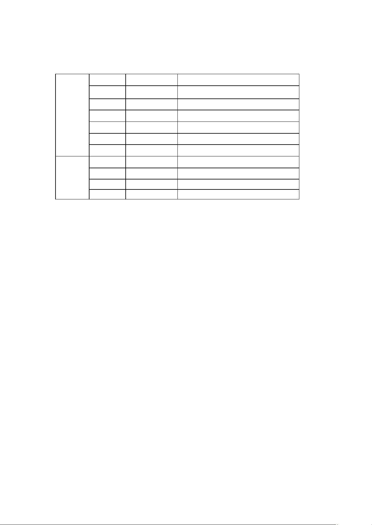
1). Laser power auto control. The circuit is as shown in Diagram 2.
Diagram 2
MT1389 has an internally integrated APC (auto optical power control) circuit. Pin 20 is the pin for
VCD laser power strength detection signal input, Pin 21 is pin for DVD laser power strength
detection signal input and Pin 23 is pin for VCD/CD laser power drive control output. When it is
detected by Pin 20 that laser output power is too strong, MT1389’s internal circuit will process it
so voltage output by Pin 23 will increase and V302 (2SB1132) conductivity will decrease,then the
collector electrode voltage will drop, the voltage supplied to the laser tube will also drop, the light
from the laser head will become weaker, thus automatically adjusting the laser power output. Pin
22 is the pin for DVD laser power drive control output and the control process is similar to that of
VCD.
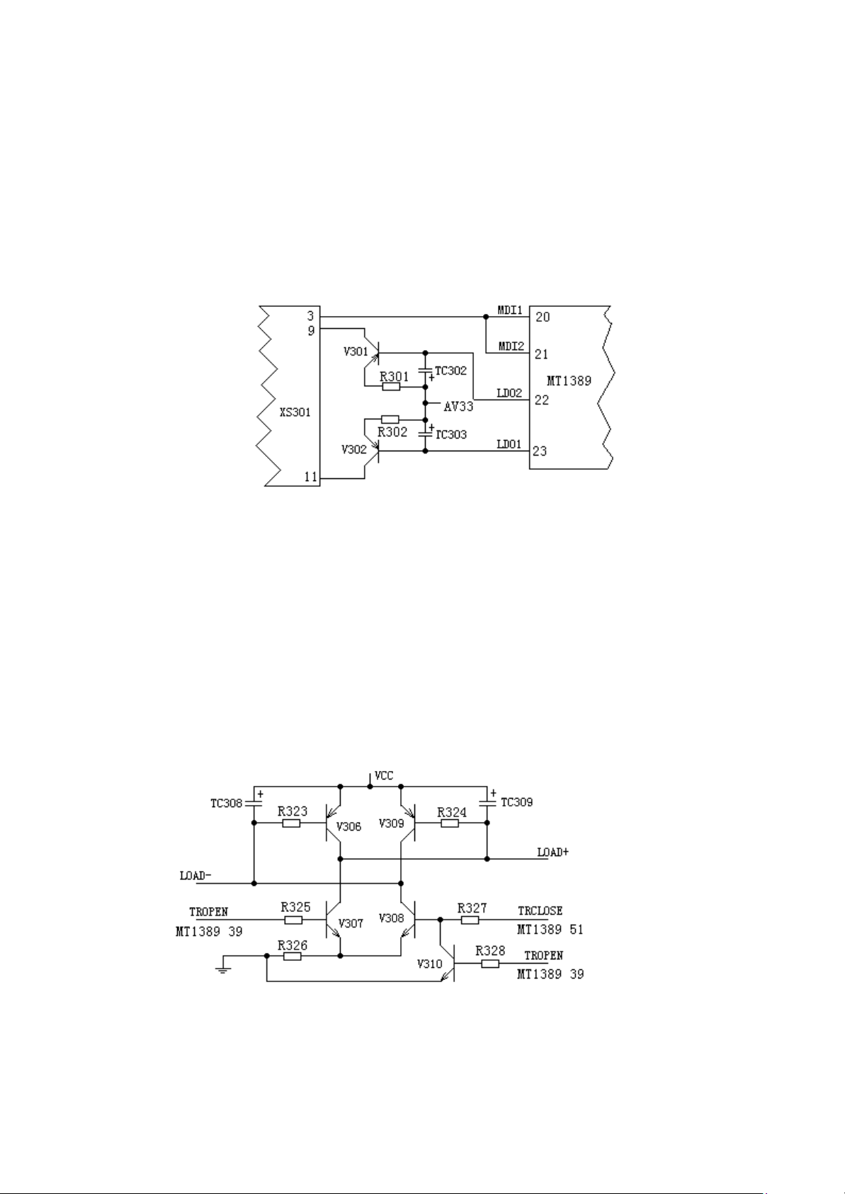
2). Inject/Eject control circuit. The circuit is as shown in Diagram 3.
Diagram 3
What is different form the previous MTK circuit is MT1389 has an internally integrated advanced
signal processing circuit, and the inject/eject control signals are processed by MT1389. The inject
control signal are processed by Pin 51 of MT1389 and the eject control signal is processed by Pin
39 of MT1389.
When we press the inject button, Pin 51 of MT1389 is high level and Pin 39 is low level. Now, the
triode V308 conducts and the passes resistance R323, making the base of V306 low level. V306
also conducts. The direction of current is as shown in the following diagram:
Power supply voltage VCC ?V306 E-C junction? motor positive end LOAD+ ?
motor negative end LOAD- ? V308 C-E junction ? ground
So the motor runs clockwise and completes the inject operation.
When we press the eject key, Pin 51 of MT1389 is low level and Pin 39 is high level. Now the
triode V307 conducts and passes resistance R324, making the base of V309 low level. V309 also
conducts. The direction of current is as shown in the following diagram:
Power supply voltage VCC ?V309 E-C junction? motor negative end LOAD+ ?
m otor positive end LOAD- ? V307 C-E junction ? ground
So the motor runs counterclockwise and completes the eject operation.
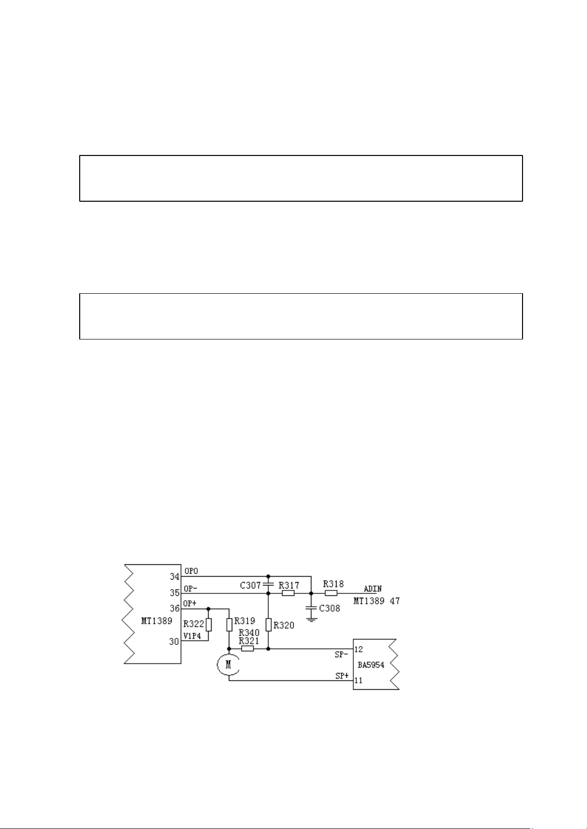
3). Main axle motor control braking circuit. The circuit is as shown in Diagram 4.
In order to extend the service life of the motor and reduce the impact of starting current on the
motor, when there is a disk, our R&D personnel design the main axle motor to be always at the
status of running, so even if “STOP” key is pressed, the disk will not stop running. This way, when
we press the “EJECT” key, a braking signal is needed to immediately stop the main axle motor
and the “EJECT” operation can be completed within a short period of time.
When it is playing, if we press the “EJECT” key, the main axle drive signal will disappear, but the
main axle motor, due to the effect of moment, will still run. At this time, the electromotive force
generated by the motor operation can obtain induction voltage on the sampling resistances R321
and R340 and, through resistances R319 and R320, adds them to Pin 36 and Pin 35 of
4
MT1389, and after internal processing and amplification in MT1389, is output from Pin 34, then
sent to Pin 47 of MT1389 via R318. After internal analog/digital conversion and corresponding
processing, MT1389 outputs a transient motor anti-braking signal from its Pin 37, thus
immediately stopping the main axle motor to ensure that the disk no longer evolves when it is
being ejected.
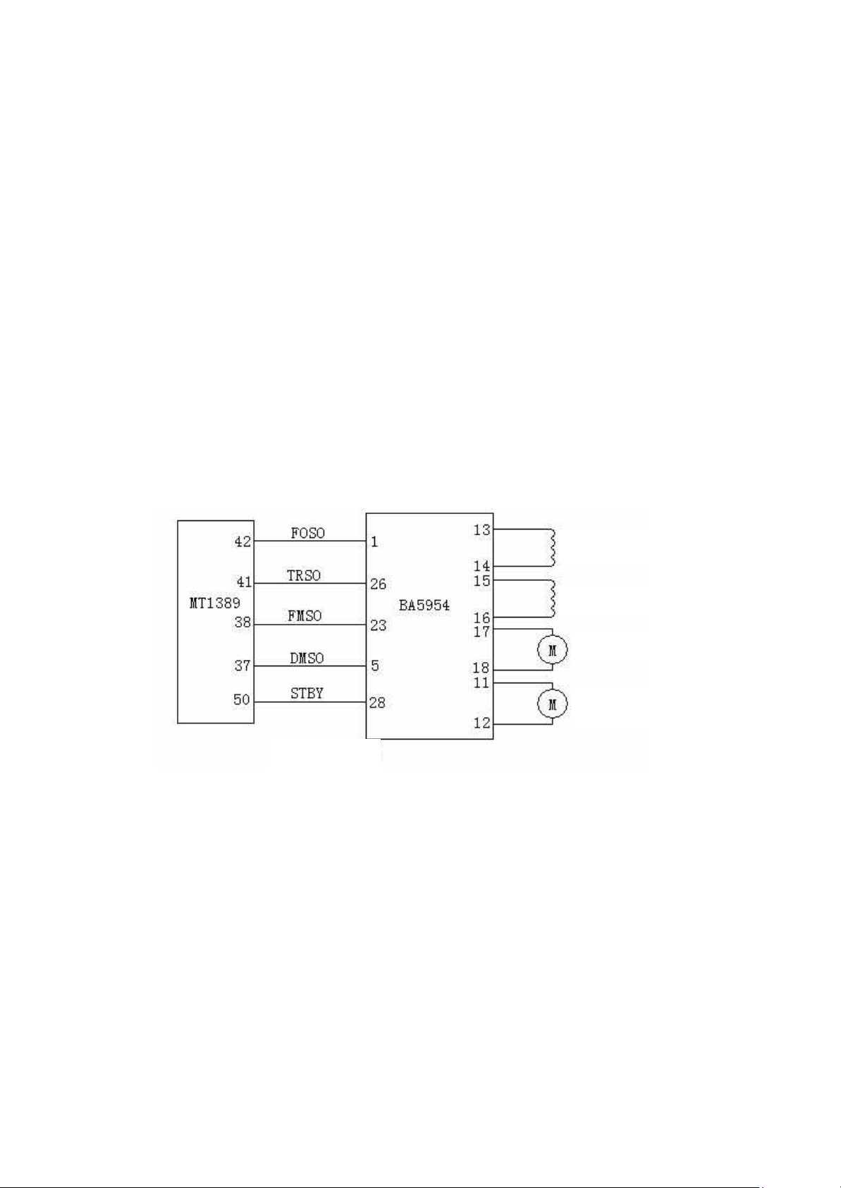
3. Servo drive circuit
The servo drive of this machine uses one 4-channel BA5954 drive circuit. This circuit is specially
designed for servo. The circuit is as shown in Diagram 5.
MT1389 digital servo circuit generates four servo control signals: Focus control signal, tracking
control signal, feed control signal and main axle control signal. These signals are respectively
added to Pin 1, Pin 26, Pin 23 and Pin 5 of BA5954. After being amplified by BA5954 drive, the
focus control signal and tracking control signal are output from Pin 13, Pin 14 and Pin 15, Pin 16
of BA5954 and then added to the focus and tracking coils to drive the laser head to complete the
focus and tracking operations.
Feed and main axle drive signals are output from Pin 17, Pin 18 and Pin 11, Pin 12 of BA5954 and
then added to the feed motor and main axle motor to drive the laser head to make radial movement
and make the disk evolve at constant linear velocity.
Focus coil
Tracking coil
Feed motor
Main axle motor
Diagram 5
Pin 28 (STBY) of BA5954 outputs enable/disable signals. Only when this pin is high level can the
output terminal outputs drive voltage.
Chapter Three Working Principle of Decoder Circuit
The decoder circuit of this machine mainly consists of the decoder chips MT1389, SDRAM
AE45164016, FLASH ROM 29LV160BE, audio frequency DAC CS4360, etc.
1. System control circuit
1). Resetting circuit is as shown in Diagram 6:
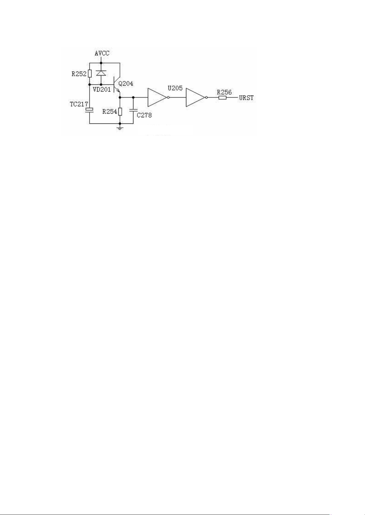
Diagram 6
The resetting circuit of this machine consists of the triode Q204 9014, resetting capacitor TC217
22uF/16V and inverter U205 HCU04. When we open the machine, because the end voltage of the
capacitor cannot change suddenly, Q204 base is low level. The emitter of Q204 is low level and,
after secondary inversion and trimming by U205, outputs low-level resetting signal to Pin 110 of
MT1389 to provide resetting for MT1389.
When charging ofTC217 is finished, Q204 base changes to high level and Q204 conducts. Its
emitter is high level and, after secondary inversion and trimming by U205, it outputs high level
and adds it to Pin 110 of MT1389 to enable it to maintain high level during normal operation.
2). Clock circuit
X201 27MHz crystal oscillator, C275/27PF, C276/27PF and inverter HCU04 form the clock
oscillation circuit. The clock signal generated passes R244 and R248 and is then added to Pin 229
and Pin 228 of MT1389 to provide MT1389 with working clock.
3). Data communication circuit
The data communication circuit of this machine mainly consists of the decoder chip MT1389,
SDRAM AE45164016 and FLASH ROM 29LV160BE. It is shown in Diagram 7.
MT1389 is a super large-scale integrated circuit, whose working voltages are +3.3V and +1.8V. Its
main functions are advanced RF small signal processing, digital servo processing, digital signal
processing, MPEG decoding, video decoding, etc. At the same time, the built -in MCU of MT1389
is also the system control circuit of complete machine.
AE45164016 is a 4M*16bit large-capacity SDRAM. Its working voltage is +3.3V. The 6ns
module used in DV971 is very fast and its maximum working frequency can reach 166MHz. As
the working buffer memory of decoder chip MT1389, its main function is to store the audio and
video data flows in the time of decoding.
29LV160BE is FLASH ROM, whose capacity is 16Mbit and working voltage is +3.3V. It is
mainly used to store user information, such as OSD characters, working micro-codes, starting
LOGO, ETC.
39 38 37 18 17 19 16 20 21
77
26 28 11 15 47 79 66 VD
RY/BY
29LV160BE
GND
2. Audio/video output circuit
1). Video output circuit
DK1050S not only outputs three interleave video signals: CVBS composite video signal, S
terminal Y-C signal and Y/Cb/Cr color difference signal, but also outputs two line-by-line video
signals: Y/Pb/Pr line-by- line color difference signal and VGA line-by-line signal.
Its decoder chip MT1389 has a built- in video encoder circuit that can directly outputs analog
composite video signal CVBS, S terminal, color-difference signal and VGA signal.
CVBS composite video signal is output from Pin 198 of MT1389; S terminal signal Y-C is output
from Pin 194 and Pin 196 of MT1389; color difference signal and R- B-G signal in VGA interface
are output from Pin 203, Pin 202 and Pin 200 of MT1389; synchronous signals HSYNC and
VSYNC of line and field in VGA interface are output respectively from Pin 207 and Pin 205 of
MT1389.
It must be noted that interleave color difference, line-by-line color difference signal and
line-by-line R- B-G signal are output from the same pin. So the corresponding signal output shall
be selected through setting according to the port connected to TV; otherwise, there might be sound
without picture.
2). Audio output circuit
After being processed by MT1389, the audio frequency signal outputs data signals of five audio
tracks from its Pin 217, Pin 218 and Pin 219, and outputs clock signals of five channels from its
Pin 214 and Pin 215. These signals, after passing IC 74HCT125, are sent to the audio frequency
signal processing IC TAS5508 for audio frequency signal processing (s ee Exhibit for detailed IC
data). After that, ten groups of PWM signals are output, six of which are sent to power
amplification, two are sent to earphone output and two sent to auxiliary channels.
Of the six groups of signals sent to the power amplification IC, the surround sound and super bass
share one N13 IC TAS5508 and the main audio track and the middle share N14 IC TAS5508.
Signals are amplified in this IC. Because it is digital high-frequency signal amplification, the
efficiency is very high and the heating value of power IC is very small. After amplification, the
BYTE
A0—A21
AD0—AD7
DCE
DRD
DWR
Diagram 7
MT1389
DMA0—DMA11
DQ0—DQ15
113
137
156
157
140
139
142
138
145
143
AE45164016
DQML
15
DQMH
CLK
CKE
RAS
CAS
CS
WE
BA1
BA0

output is still digital signal, so in order for output in the speaker, the amplified digital signal shall
be processed before output.
For a PWM signal that contains audio frequency signals, because the high-frequency signal’s
frequency is very high and exceeds the hearing of human ear, so we can neglect the influence of
high-frequency signals in the process of processing and only restore low-frequency audio
frequency signals.
TAS5508 is an advanced 8-channel digital high-performance IC modulated by pulse width. It applies
to processing of most audio frequency digital signals and presents good noise coefficients and
dynamic range within 20— 20KHZ. Its characteristics are as follows:
(1) Auto control over clock speed and data sampling speed;
(2) 8 groups of channels for audio frequency input;
(3) 8 groups of PWM output that can be configured into 6-channel stereo sound output line or
8-channel line output;
(4) Line output is one group of PWM signals drives one different input open-loop amplifier.
IC TAS5112 is a high-performance audio frequency digital power amplifier. When bridged with a
6-ohm load, each channel can output up to 50W and has a 95DB dynamic range. The distortion is
low and power efficiency can reach 90%. The heating value is low. It provides low-voltage
protection, hi-temperature protection, over-current protection, etc, and has a built- in drive power
adjustment door circuit. It is suitable for home theaters, DVD receivers, mini composite acoustics,
etc. Please see the appendix for detailed introduction to IC.
When the disk is normally read, the digital signals and clock signals processed from 1389, after
selection by IC 74HCT125, are sent to Pins 26-31 of IC TAS5508 for processing. Now, plug in the
earphone, the PH-SEL is high level and MUTE, when normally working, is also high level. Pin 37 of
TAS5508 is also high level. The oscilloscope can detect all data lines and clock lines. Of the signals
from 5508, one group is sent to N8 and N9 and, after processing, is output from the auxiliary channel;
one group is sent to the earphone for processing; PWM signals are sent to the amplifier for
amplification.
When the earphone is plugged in, the PH-SEL signal is peremptorily short circuited to the earth and
changes to low level. The amplifier is mute, but the auxiliary channel output is normal.
When reading the disk, the system by default selects Karaoke for input. So, when playing the disk,
Karaoke can be opened and this machine also has the auto accompaniment function that is realized
by software. When playing VCD, if the system detects external input, it automatically shields the
human voice signal in the disk and only keeps the accompanying sound.
DK1050S has the radio function and can receive RDS signals. Radio head control lines CE, DI, CL
and DO, through 28P drop-out lines, are respectively connected to MT1389. When any control line is
abnormal, radio function will become abnormal. The RDS signal received by the radio head is sent
to special-purpose IC SAA6588 for processing.
3. Auxiliary channel, optical fiber and co-axial input
This machine has auxiliary channels, radio function, optical fiber and co-axial external input. This
machine has radio function, and auxiliary channel input function and Kar aoke function. All external
input shall be selected by N3 CD4052 and then undergo the analog/digital conversion via N7
CS5340 and be sent to MT1389 for signal processing. Subsequent processing and output share the
same process as normal disk reading signal output.
Optical fiber and co-axial signals, after inductance filtering and capacitance filtering, are sent to the

serial audio frequency digital signal to receive the input Pins 4, 12 and 14 of signal IC CS8415. After
passing this IC, the serial audio frequency digital signal is converted into PCM signal, which is then
output from Pin 16 (sampling rate signal), Pin 17 (clock signal of main track) and Pin 18 (audio
frequency digital signal) of IC and sent to IC 1389 for signal processing.
Chapter Four Wor king Principle of power board
This machine has two groups of power supply. One group supplies power for the decoder board and
small-power IC; the other group supplies power for the power amplification IC and the voltage is
high. But both groups have the same design principle.
Introduction to the principle of circuit
The 220V AC current passes the power plug, protector tube, varistor R501 and common mode
rejections BC501 and L501 and is added to the integrated bridge rectification circuit. The diode is
IN4007 that has a good performance/price ratio and has a higher durable pressure than IN4001. After
bridge rectification, 311V is output and flows through TC501 filter, then is respectively added to two
transformers and sent to the DRAIN control pin of switch modules U501 and U502.
The power supply working voltage of IC is directly rectified, filtered, divided by the resistor and
then supplied to IC. Diode D508, capacitor C516 and resister R516 form the absorb circuit to
provide windings 1-4 of the transformer with the discharge circuit for reverse electromotive force.
Pin FB controlling the IC is the feedback control pin. According to its current, the pulse width’s
conduction and starting and ending time are determined to ensure the stability of voltage output.
Five branch circuits are coupled to secondary via the transformer.
1. Voltage output from Pins 11 and 13 of transformer T502, after being rectified and filtered,
outputs a group of +28V voltage for power amplification IC;
2. Voltage output from Pin 16 of transformer T501, after being rectified and filtered, outputs
a group of +12V voltage that, after being rectified by IC LM7805, outputs a group of +5V
voltage;
3. Voltage output from Pin 14 of transformer T501, after being rectified and filtered,
outputs a +5V volt age to supply one end of coupling amplifier U502;
4. Voltage output from Pin 12 of transformer T501, after being rectified and filtered, outputs
a +3.3V voltage and to supply a group of stable voltages for CPU;
5. Voltage output from Pin 9 of transformer T501, after being rectified and filtered, outputs a
group of 21V voltage for displayer driver IC. Clamp ZD501 on -21V supplies panel
display screen with filament voltage. Voltage to ground of FL+ and FL- is about -16V.
Because the two groups of power switches of the machine have different working principles, here
we only analyze the group that supplies CPU with +5V voltage.
Feedback sampling of this group of power supply comes from 5V. It supplies the coupling
amplifier HS817 via D514 and R517. At the same time, it is divided by R519 and R520 to supply
the reference voltage pin R of 2.5V comparator. When 5V is high, the Pin KA of comparator
LM17431A conducts, passes photoelectrical coupler HS817 and is sent to the fourth pin of switch
IC 5L0380R to reduce the conduction time of internal switch tube, reduce the coupling of
transformer, lower the 5V output and achieve the goal of automatic regulation and vice versa.
It must be noted that, in this power switch, the two groups of power switches use a base voltage
that is different from IC. The group supplying the amplifier outputs a higher voltage, so it uses
LM431 that has better performance and a higher endurable pressure. However, the group
1 2
supplying 3.3V voltage, because the output voltage is low, uses 17431. Because these two kinds of
IC are different, care shall be taken in the process of maintenance to avoid confusion.
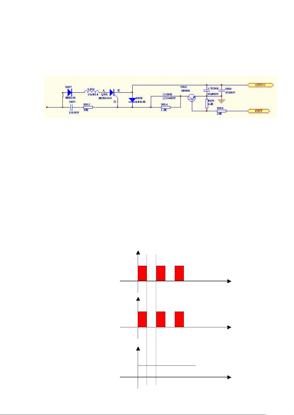
This machine uses DC switches.
When the power of the machine is just on, voltage output from Pin No.16 of transformer, after
being rectified by D507 half wave, generates a 76V high-frequency voltage on silicon-controlled
pin 1. This voltage passes capacitors C507 and R513 and is coupled to Pin No.3 of Q501, the same
high-frequency voltage. Because of the effect of feedback stable voltage, Pin No.2 of Q501 gets a
stable 5V DC voltage. Its wave shape is as follows:
It can be seen from the above diagram that when T=t01, Pin P1 of Q501is high level and Pin P3 of
Q501 is also high level and Q501 deducts and Pin P3 outputs a 5V DC voltage; when T=t12, Pin
P1 of Q501 and Pin P3 of Q501 are low level and, because U2 > U1, Q501 stops and Pin P3 does
not output voltage and 5 VDC voltage is supplied by capacitor TC505;
At the moment the power is on, the voltage of U1 is 76V. But, because the conduction of
silicon-controlled, Pin P2 of Q501shall be maintained at 5V causing the voltage of U1 to drop to
around 7V, so other secondary windings do not output. Power switch only outputs CPU5V and the
power supply is at the low -load working status.
When the machine is open, only 5V is supplied to the panel via transformer coupling and the
complete machine is stand-by. When pressing the stand-by on the panel or on the remote controller,
Pin 40 of panel IC TP6317 outputs a high level and triode V503 conducts, giving Pole G of Q501a
low level and silicon-controlled Q501 stops. Triode V504 conducts and triode V502 stops. Other
windings begin to work normally.
U1
0
t
U3
t
U2
t
Chapter Five Panel Control and VFD Display Circuit
IC TP6317
The panel mainly consists of the VFD display screen, drive IC TP6317, remote receiving head
HSOO38A2, keys control and indicator display circuit. It mainly accomplishes the man-machine
dialogue and displays the working status.
Diagram of components is as follows:
VFD
display
Under the control of built-in CPU of MT1389 and via VFDST (status), VFDCK (clock) and
VFDAT (data), U401 IC TP6317 is controlled to display complete-machine working status and
receive the user control command given by TP6317 to control the complete-machine control
circuit and enable complete machine to work under designated status.
When pressing the user operating panel key, the control command via the key scans the circuit and
sends control command to IC TP6317. After internal encoder drive of IC TP6317, control data is
output from Pin 5 and Pin 6 (VFDAT) to internal CPU of MT1389 and the CPU controls the
controlled circuit and controls VFD via IC TP6317.
VFD401 is a vacuum fluorescent display screen. Its most obvious feature is height. Its working
principle is similar to TV display tube. Pins 1, 2, 34 and 35 supply the filament; Pins 27-32 supply
the GRID poles. In each GRID there are 16 different characters for display. Pins 4-19 are SEG
poles. CPU, through controlling IC TP6317, finally controls SEG poles, thus enabling the
characters of working status to display on the display screen.
Remote receiving head circuit mainly consists of remote receiving head HS0038A2. Pin No.1 is
for grounding, Pin No.2 is the supply end and Pin No.3 is the output pin for received signals and is
directly connected to the CPU inside MT1389 to control corresponding circuit.
This machine has the earphone output function. One of the pins inside the earphone is directly
connected to TAS5508. When the earphone is plugged in, detection line H-DET is grounded and
becomes low level. When Pin 12 of TAS5508 becomes low level, the amplifier partially outputs
mute; when it works normally, the detection pin is high level (about 3.3V).
Key control
U401
Panel indicator control
VFDST
VFDCK
VFDAT
U201
MT1389
Remote
receiving
 Loading...